Interpreting Ideality Factors for Planar Perovskite Solar ...

This journal is©The Royal Society of Chemistry 2015 Chem. Commun.
Cite this:DOI: 10.1039/c5cc03666f
Recent advances in flexible perovskite solar cells
B. Susrutha,a Lingamallu Giribabuab and Surya Prakash Singh*ab
Flexible and low-weight thin-film perovskite solar cells have attracted considerable attention for
developing large-area, roll-to-roll and differently shaped photovoltaics with improved power conversion
efficiencies. In this review, we describe how researchers have adopted different approaches to enhance
the device performance of the flexible perovskite solar cells to compete with rigid substrates with
tailored electron/hole transport materials and flexible substrates.
1. Introduction
Solar energy is one of the most abundant and renewable energysources and has minimum harmful impact on the environmentcompared to other sources like fossil fuels and nuclear energy.A solar cell (also called a photovoltaic cell or a photoelectriccell) is a solid-state electrical device that directly converts solar
energy into electricity. An ideal solar cell requires low-cost,trouble-free, abundant material resources with good stabilityand high power conversion efficiency (PCE), and should also beable to be integrated into a large area device. Based on this criteria,many photovoltaic technologies have been developed such ascrystalline silicon based solar cells;1–4 thin-film vapour-depositedsemiconductor-based solar cells, for example, CdTe or CIGS;5,6 andsolution-processed solar cells based on organic semiconductors,hybrid composites, or inorganic semiconductors,7–13 which aredenoted as first, second, and third generation photovoltaics(PVs), respectively. Moreover, crystalline Si-based solar cellsplay a major role in the commercial photovoltaic market and
a Inorganic and Physical Chemistry Division, CSIR-Indian Institute of Chemical
Technology, Uppal Road, Tarnaka, Hyderabad-500607, Telangana, Indiab Network Institute of Solar Energy, (CSIR-NISE) and Academy of Scientific and
Innovative Research (AcSIR), New Delhi, India. E-mail: [email protected]
B. Susrutha
Dr B. Susrutha is a ResearchAssociate at the CSIR-IndianInstitute of Chemical Technology,Hyderabad, India, in the group ofDr L. Giribabu and Dr SuryaPrakash Singh. She gained hermasters at Osmania University,Hyderabad, and then received herPhD from the Indian Institute ofTechnology, Kharagpur, in 2014.Her research interests are focusedon the synthesis and fabricationof perovskite solar cells, andthe synthesis of nanofluids andnanocomposites.
Lingamallu Giribabu
Lingamallu Giribabu receivedhis PhD degree in chemistry fromthe University of Hyderabad in2000. Before joining the CSIR-Indian Institute of ChemicalTechnology, Hyderabad, India, asa Scientist in 2003, he workedwith Dr. Martin R. Johnston(Central Queensland University,Australia) and Prof. Karl M.Kadish (University of Houston,Houston, USA) as a postdoctoralfellow. He has been working as asenior scientist at the Indian
Institute of Chemical Technology, India, since 2003. His researchinterests include the development of low-cost new efficient materialsfor dye-sensitized solar cells, donor–acceptor systems, and the non-linear optical properties and photoelectrochemistry of tetrapyrroliccompounds. He has published over 100 research articles, patents,review articles and a book chapter.
Received 2nd May 2015,Accepted 6th July 2015
DOI: 10.1039/c5cc03666f
www.rsc.org/chemcomm
ChemComm
FEATURE ARTICLE
View Article OnlineView Journal

Chem. Commun. This journal is©The Royal Society of Chemistry 2015
have efficiencies of 12% to 16%. However, their high manu-facturing costs limit their use in large-scale PVs. Recently,perovskite solar cells has promised to break the current para-digm by ultimately combining both low cost and high efficiency.Following the pioneering work by Gratzel et al. on the discovery of9.7% solid-state perovskite solar cell, which has attained 500 hverified stability, more interest is now being shown by researchersin this area.14,15
In general, fluorine-doped tin oxide (FTO) or indium tinoxide (ITO) coated glass substrates are used for the fabricationof solar cells, which provide an extremely effective barriertowards water and oxygen penetration into the solar cell device,but they require high-temperature processes to fabricate PVswith excellent PCEs.14–18 However, the main drawbacks of this typeof substrates concern their rigidity, weight, and frangibility, whichlimit the potential integration of PV devices into large-scale androll-to-roll modules. Instead, flexible substrates can be easilymoulded into different shapes, and thin-film PV panels containingthese substrates can be integrated with infrastructures of variousshapes and sizes for innovative energy-generating products.Hence, nowadays, researchers have focused more on designinglow-cost, lightweight, and mechanically flexible thin-film PVs,which enable the implementation of portable, reduced dimen-sions, and also roll-to-roll fabrication of solar devices on a largescale.19–31 To date, a lot of different PV materials have beendeveloped with various deposition methods on a variety of sub-strates for the manufacture of flexible solar cells. Based on thePV materials used, flexible solar cells are usually categorized as (1)Si-based flexible solar cells; for example, amorphous Si-basedPVs,32–35 polycrystalline Si-based PVs,36–38 and monocrystallineSi-based PVs,39–41 (2) compound flexible solar cells; for example,CdTe,42–44 Cu(In,Ga)Se2 (CIGS),45–47 and III–V semiconductors,48–50
(3) organic solar cells; for example, dye-sensitized solar cells,51–54
or (4) organic–inorganic hybrid solar cells; for example, Siwith poly(3,4-ethylenedioxythiophene):poly(styrenesulfonic acid)(PEDOT:PSS), ZnO with poly(3-hexylthiophene) (P3HT), and
perovskite solid-state solar cells.55–61,99,105 In this review, wefocus our attention on the progress that has been made in thefield of flexible perovskite solar cells.
2. Crystal structure and mechanism ofperovskite solar cells
Perovskite materials have a specific crystal structure with theABX3 formula (X = oxygen, halogen). The larger A cationoccupies a cubo-octahedral site shared with twelve X anions,whereas the smaller B cation is stabilized in an octahedral siteshared with six X anions. Organic–inorganic halide perovskitesmaterials are usually used for solar energy applications. Herein,the larger A cation is organic; it is generally methylammonium(CH3NH3
+) and the X anion is a halogen, generally iodine,although Br and Cl are also commonly used. For efficient cells,cation B, Pb is universally used. The crystal structure of the organic–inorganic perovskite is shown in Fig. 1. A typical perovskite isthus CH3NH3PbX3, with the mixed halides CH3NH3PbI3�xClx
and CH3NH3PbI3�xBrx also being important.The basic device architecture of the perovskite solar cell
consists of a FTO- or ITO-coated glass substrate deposited withcompact TiO2 and mesoporous TiO2 or Al2O3 as the electron-transport material (ETM) and then coated with perovskite,followed by a hole transport material (HTM), usually 2,2 0,7,7 0-tetrakis(N,N-di-p-methoxyphenylamine)9,90-spirobifluorene (spiro-OMeTAD), and furthermore an Au/Ag metal layer as the electrode.When the device is irradiated under solar light, the perovskitematerial absorbs light and ejects an electron into the conduc-tion band (CB) of the TiO2 film with an energy gap Eg B 1.5 eV.It has been shown that the electrons can easily transfer fromCH3NH3PbI3 to the CB of the TiO2 film, and the holes thusgenerated in CH3NH3PbI3 transfer to the HTM layer. In mixed-halide perovskites, Al2O3 plays a significant role and acts as amesoporous scaffold for the perovskites. When CH3NH3PbI2Clis irradiated, the photogenerated electrons cannot inject into theAl2O3 film due to the very large band gap (Eg B 7–9 eV) of Al2O3
and the holes produced in the perovskite are thus transported tothe HTM layer. A schematic of the perovskite solar cell architec-ture is shown in Fig. 2.
Fig. 1 Structural representation of an organic–inorganic perovskite(Michael Gratzel in ref. 62).
Surya Prakash Singh
Dr Surya Prakash Singh is ascientist at the CSIR-IndianInstitute of Chemical Technology,Hyderabad, India. He studiedchemistry at the University ofAllahabad, India, and obtainedhis PhD in 2005. After working atthe Nagoya Institute of Technology,Japan, as a postdoctoral fellow, hejoined Osaka University, as anAssistant Professor. He worked asa researcher in the PhotovoltaicMaterials Unit, National Institutefor Materials Science (NIMS),
Tsukuba, Japan. He has been involved in the design and synthesisof materials for organic solar cells and flexible devices. He haspublished over 100 papers and reviews in peer-reviewed journals.
Feature Article ChemComm
View Article Online
This journal is©The Royal Society of Chemistry 2015 Chem. Commun.
3. Why perovskite solar cells areimportant?
Perovskite materials possess a high extinction coefficient overthe visible spectrum and low exciton binding energy, whichmake them superior light harvesters for photovoltaic applicationswithin the nano-scale.63–65 The main advantage of the perovskitesolar cell is the high output voltage close to the optical band gap,which reduces the energy redundancy that exists in most excitonicsolar cells like organic PVs.16,66,67 Since perovskite shows anambipolar nature, which means it can work as either an electronor a hole transporter, it allows for a versatile design of devicearchitectures. For example, Bi et al. used perovskite as an electrontransporter to form a junction in contact with various HTMs.68
Lee et al. deposited perovskite on the surface of meso-structuredAl2O3 layers, where Al2O3 acted as a non-injecting electrodescaffold and perovskite as the electron-transport medium.16 Etgaret al. observed that perovskite can play the role of a light harvesterand a hole conductor by applying it in contact with an electronacceptor (TiO2) to realize a charge separation junction.69,70
In the early 1990s, Mitzi, and co-workers carried out extensiveinvestigations into the optoelectronic properties of organic–inorganic perovskites. Their research focused on layered organo-metal perovskites that exhibited strong excitonic features anddemonstrated good operation in transistors and light-emittingdiodes.71–73 In 2009, Kojima et al.74 first attempted to use methyl-ammonium lead halide (CH3NH3PbX3) as a semiconductor sensi-tizer in dye-sensitized solar cells and achieved a PCE of 3–4%,which was, however, a much low efficiency compared to thatachieved with conventional Ru-based molecular dyes with PCEsof more than 11%.75 Two years later, Park’s group65 reported a6.5% efficient CH3NH3PbI3 perovskite solar cell, which was slightlymore stable in electrolytes, and they showed its use in moreadvanced technology to form the perovskite sensitizer on a thinnerTiO2 film. Currently, the performance of perovskite-based solarcells has rapidly improved with a PCE as high as 20.1% accordingto National Renewable Energy Laboratory efficiency chart.
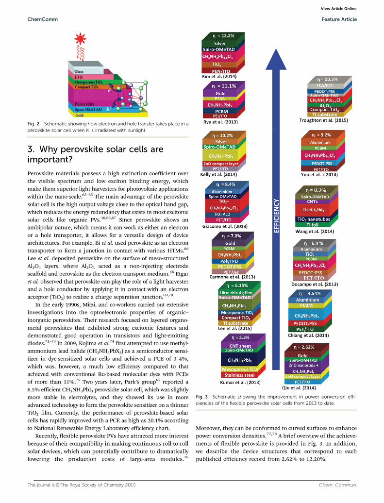
Recently, flexible perovskite PVs have attracted more interestbecause of their compatibility in making continuous roll-to-rollsolar devices, which can potentially contribute to dramaticallylowering the production costs of large-area modules.76
Moreover, they can be conformed to curved surfaces to enhancepower conversion densities.77,78 A brief overview of the achieve-ments of flexible perovskite is provided in Fig. 3. In addition,we describe the device structures that correspond to eachpublished efficiency record from 2.62% to 12.20%.
Fig. 2 Schematic showing how electron and hole transfer takes place in aperovskite solar cell when it is irradiated with sunlight.
Fig. 3 Schematic showing the improvement in power conversion effi-ciencies of the flexible perovskite solar cells from 2013 to date.
ChemComm Feature Article
View Article Online

Chem. Commun. This journal is©The Royal Society of Chemistry 2015
4. Low-temperature approach formaking TiO2 films over flexible substrates
In general, solar cell architectures with mesostructured TiO2 orAl2O3 scaffold have typically shown superior efficiency andstability on glass substrates upon annealing at high tempera-tures.79–83 The Al2O3 layer does not require careful annealingsince no charge injection occurs in Al2O3.84 The development oflarge-scale devices requires low temperatures to yield highquality compact hole blocking layers and well-connected meso-porous nanocrystalline materials, which is applicable to plasticsubstrates to attain enhanced efficiencies.85 Recently, Zardettoet al.86 proposed a UV irradiation process on a customizedTiO2 nanoparticle paste for the fabrication of efficient flexibledye-sensitized solar cells. The atomic layer deposition (ALD)method has also been used for the fabrication of ultra-thin,uniform, and conformal layers at low temperatures in several PVtechnologies.87 The plasma approach offers several advantagesover conventional thermal processes, in particular it enables thedeposition of higher quality films, i.e. in terms of lower pinholedensity in the range of temperatures compatible with conductiveplastic substrates.88 Recently, Giacomo et al.89 prepared a compactTiO2 layer/scaffold at low temperature (150 1C) by UV irradiation incombination with ALD to fabricate flexible perovskite solar cells onan ITO-coated poly(ethylene terephthalate) (PET) substrate with anactive area of 0.12 cm2 with a PCE of 8.4%. This value was lowcompared to glass/ITO-based devices (9.9%), wherein the scaffoldwas prepared by thermal annealing at 450 1C.
After developing the most efficient compact layer/scaffoldcombination at the cell level, they subsequently scaled up theprocess over large areas for the fabrication of a flexible photovoltaicmodule consisting of four series-connected cells on a 5.6 � 5.6 cmPET/ITO substrate, which is shown in Fig. 4. For this, they used ascreen printable mesoporous scaffold and patterning procedurescompatible with the delicate PET/ITO substrates. The preparedmodule exhibited a PCE of 3.1%, with a fill factor of 71%, an opencircuit voltage (Voc) of 3.4 V, and a short circuit current density ( Jsc)of 5.2 mA cm�2. The obtained device showed good mechanicalresistance to the bending test and maintained its initial PCE after asequence of 100 bending cycles at large radii of curvature. Atsmaller radii (o5 mm), the PCE significantly decreased becauseof the increased sheet resistance, which might be due to theformation of cracks in the brittle ITO.90 These in turn coulddamage the active layers over the ITO, leading to a lower PCE.
In another report, Kim et al.91 fabricated highly bendable (up to1 mm bending radius) mixed-halide perovskite (CH3NH3PbI3�xClx)
solar cells based on polyethylene naphthalate (PEN)-depositedITO flexible substrates with an excellent PCE of 12.2%. This isthe highest PCE reported to date in flexible perovskite solar cells.Herein, a B20 nm-thick amorphous TiOx compact layer wasdeposited on PEN/ITO substrate via a plasma enhanced-ALD(PEALD) technique. They observed a high photocurrent density ofmore than 20 mA cm�2, which was responsible for the high PCEand attributed to the superior recombination-blocking and electron-transport properties of the PEALD-TiOx layer. A cross-sectionalscanning electron microscopy (SEM) image with an image of thedevice is shown in Fig. 5(a and b). As shown in Fig. 6, this solar cellshows superior mechanical endurance properties, i.e., its energyconversion efficiency does not change after 1000 cycles of bendingtests under conditions of a bending radius of 10 mm, demonstrat-ing that using the ALD technique for the preparation of scaffoldnanolayers at low temperature is a good initiation to produceefficient flexible perovskite solar cells, which can potentially be usedfor a power solution for future wearable devices.
5. ZnO-based flexible perovskite solarcells
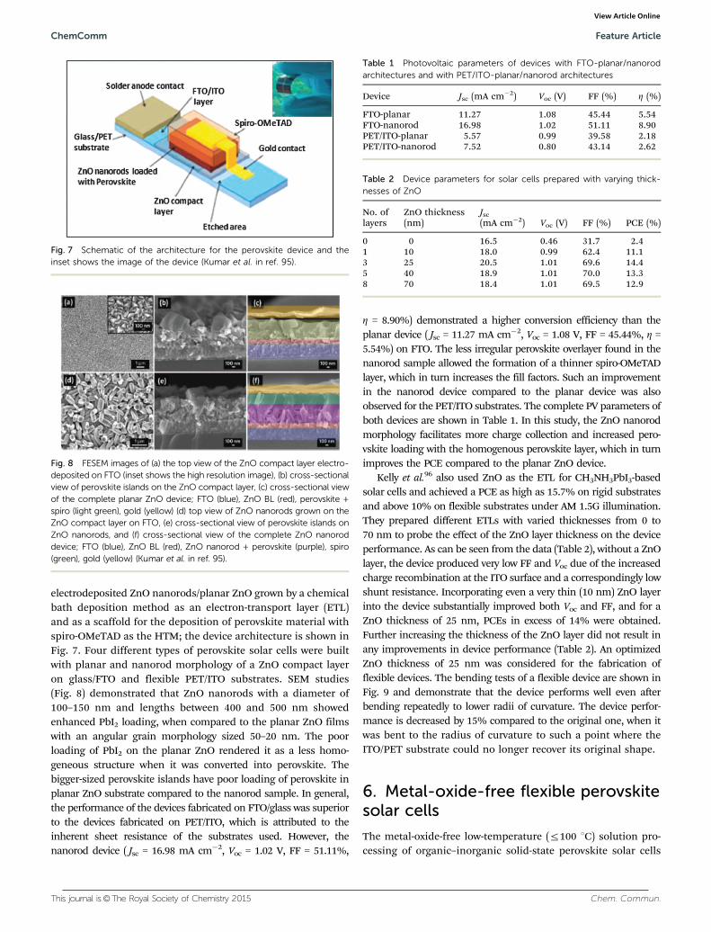
ZnO is a feasible alternative to TiO2/Al2O3 due to its comparableenergy levels as well as good electron-transport properties.92–94
In addition, a ZnO nanoparticle layer can be deposited easily byspin-coating and requires no heating or sintering step, whichmakes it ideal for deposition on thermally sensitive substrates.Based on this, Kumar et al.95 synthesized flexible and low-temperature (o100 1C) solid-state perovskite CH3NH3PbI3 solarcells with a PCE of 8.90% on FTO-based glass substrates and aPCE of 2.62% on flexible PET/ITO-based substrates. They used
Fig. 4 Image of the four cell series-connected module (5.6 � 5.6 cm)(Giacomo et al. in ref. 89).
Fig. 5 (a) Cross-sectional SEM image of the perovskite planar hetero-junction flexible solar cell and schematic of the flexible device structure. (b)An actual bent image (Kim et al. in ref. 91).
Fig. 6 Normalized PCE of flexible perovskite devices as a function ofbending cycles with different radii of 400, 10, and 4 mm. The inset showsthe real images taken during the bending tests. The error bar representsthe standard deviation from four devices (Kim et al. in ref. 91).
Feature Article ChemComm
View Article Online
This journal is©The Royal Society of Chemistry 2015 Chem. Commun.
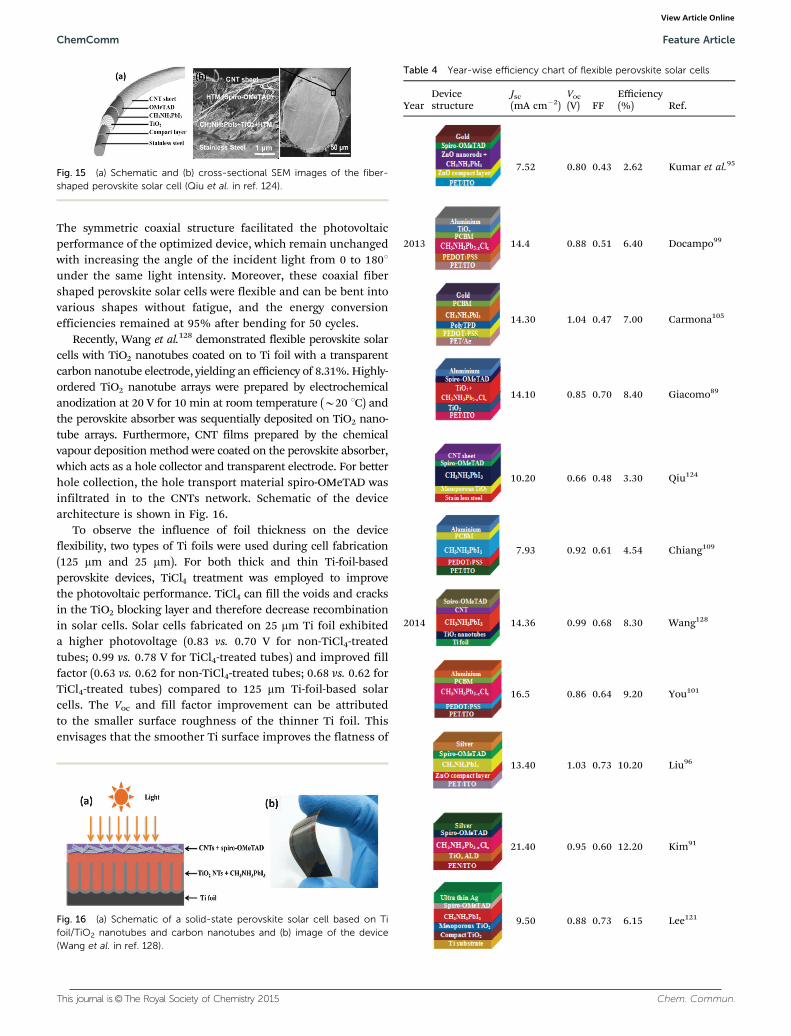
electrodeposited ZnO nanorods/planar ZnO grown by a chemicalbath deposition method as an electron-transport layer (ETL)and as a scaffold for the deposition of perovskite material withspiro-OMeTAD as the HTM; the device architecture is shown inFig. 7. Four different types of perovskite solar cells were builtwith planar and nanorod morphology of a ZnO compact layeron glass/FTO and flexible PET/ITO substrates. SEM studies(Fig. 8) demonstrated that ZnO nanorods with a diameter of100–150 nm and lengths between 400 and 500 nm showedenhanced PbI2 loading, when compared to the planar ZnO filmswith an angular grain morphology sized 50–20 nm. The poorloading of PbI2 on the planar ZnO rendered it as a less homo-geneous structure when it was converted into perovskite. Thebigger-sized perovskite islands have poor loading of perovskite inplanar ZnO substrate compared to the nanorod sample. In general,the performance of the devices fabricated on FTO/glass was superiorto the devices fabricated on PET/ITO, which is attributed to theinherent sheet resistance of the substrates used. However, thenanorod device ( Jsc = 16.98 mA cm�2, Voc = 1.02 V, FF = 51.11%,
Z = 8.90%) demonstrated a higher conversion efficiency than theplanar device ( Jsc = 11.27 mA cm�2, Voc = 1.08 V, FF = 45.44%, Z =5.54%) on FTO. The less irregular perovskite overlayer found in thenanorod sample allowed the formation of a thinner spiro-OMeTADlayer, which in turn increases the fill factors. Such an improvementin the nanorod device compared to the planar device was alsoobserved for the PET/ITO substrates. The complete PV parameters ofboth devices are shown in Table 1. In this study, the ZnO nanorodmorphology facilitates more charge collection and increased pero-vskite loading with the homogenous perovskite layer, which in turnimproves the PCE compared to the planar ZnO device.
Kelly et al.96 also used ZnO as the ETL for CH3NH3PbI3-basedsolar cells and achieved a PCE as high as 15.7% on rigid substratesand above 10% on flexible substrates under AM 1.5G illumination.They prepared different ETLs with varied thicknesses from 0 to70 nm to probe the effect of the ZnO layer thickness on the deviceperformance. As can be seen from the data (Table 2), without a ZnOlayer, the device produced very low FF and Voc due of the increasedcharge recombination at the ITO surface and a correspondingly lowshunt resistance. Incorporating even a very thin (10 nm) ZnO layerinto the device substantially improved both Voc and FF, and for aZnO thickness of 25 nm, PCEs in excess of 14% were obtained.Further increasing the thickness of the ZnO layer did not result inany improvements in device performance (Table 2). An optimizedZnO thickness of 25 nm was considered for the fabrication offlexible devices. The bending tests of a flexible device are shown inFig. 9 and demonstrate that the device performs well even afterbending repeatedly to lower radii of curvature. The device perfor-mance is decreased by 15% compared to the original one, when itwas bent to the radius of curvature to such a point where theITO/PET substrate could no longer recover its original shape.
6. Metal-oxide-free flexible perovskitesolar cells
The metal-oxide-free low-temperature (r100 1C) solution pro-cessing of organic–inorganic solid-state perovskite solar cells
Fig. 7 Schematic of the architecture for the perovskite device and theinset shows the image of the device (Kumar et al. in ref. 95).
Fig. 8 FESEM images of (a) the top view of the ZnO compact layer electro-deposited on FTO (inset shows the high resolution image), (b) cross-sectionalview of perovskite islands on the ZnO compact layer, (c) cross-sectional viewof the complete planar ZnO device; FTO (blue), ZnO BL (red), perovskite +spiro (light green), gold (yellow) (d) top view of ZnO nanorods grown on theZnO compact layer on FTO, (e) cross-sectional view of perovskite islands onZnO nanorods, and (f) cross-sectional view of the complete ZnO nanoroddevice; FTO (blue), ZnO BL (red), ZnO nanorod + perovskite (purple), spiro(green), gold (yellow) (Kumar et al. in ref. 95).
Table 1 Photovoltaic parameters of devices with FTO-planar/nanorodarchitectures and with PET/ITO-planar/nanorod architectures
Device Jsc (mA cm�2) Voc (V) FF (%) Z (%)
FTO-planar 11.27 1.08 45.44 5.54FTO-nanorod 16.98 1.02 51.11 8.90PET/ITO-planar 5.57 0.99 39.58 2.18PET/ITO-nanorod 7.52 0.80 43.14 2.62
Table 2 Device parameters for solar cells prepared with varying thick-nesses of ZnO
No. oflayers
ZnO thickness(nm)
Jsc
(mA cm�2) Voc (V) FF (%) PCE (%)
0 0 16.5 0.46 31.7 2.41 10 18.0 0.99 62.4 11.13 25 20.5 1.01 69.6 14.45 40 18.9 1.01 70.0 13.38 70 18.4 1.01 69.5 12.9
ChemComm Feature Article
View Article Online

Chem. Commun. This journal is©The Royal Society of Chemistry 2015
provides a new route to synthesize flexible large-scale and roll-to-roll hybrid solar cells. In addition to metal oxides, one ofthe fullerene derivatives, phenyl-C61-butyric acid methyl ester(PCBM), has attracted more interest as an n-type material foruse in solar cells and has already been utilized in the P–I–Narchitecture.97–104 PCBM layers deposited on perovskites caneffectively passivate the charge trap states and eliminate thenotorious photocurrent hysteresis, which produces enhancedPCEs. In this perspective, Carmona et al. reported a perovskitesolar cell based on a flexible PET substrate coated with atransparent silver electrode, PEDOT:PSS as HTM, and PCBM asthe electron-transport layer (ETL) with a gold top electrode.105
The cross-sectional SEM image with an image of this device isshown in Fig. 10.
The J–V characteristics of a typical small area (0.12 cm2)flexible perovskite solar cell measured under light intensities of100 mW cm�2 showed Jsc, Voc and FF of 14.3 mA cm�2, 1.04 Vand 0.47, respectively, leading to a PCE of 7%. Previously,Malinkiewicz et al. reported values on glass substrates withJsc, Voc and FF of 16.1 mA cm�2, 1.05 V and 0.67, respectively,leading to a PCE of 12%.100 Hence, the main difference betweenthe devices on the glass substrates and on the flexible foils isthe lower FF, which causes a strong reduction in the PCE. Thereduction in FF and PCE is due to the thicker hole and electronblocking layers in the flexible cells. This can be avoided when alarger substrate is used in either a batch or roll-to-roll process.Moreover, this solar cell is very strong, leading to a slightdecrease in PCE of only 0.1% after 50 bending cycles.
An inverted flexible perovskite soar cell with PEDOT:PSS as ahole selective contact and a PCBM layer as the n-type contactwas developed by Docampo et al.,99 and its device architectureis shown in Fig. 11. To examine the performance of the invertedarchitecture, they designed regular as well as inverted perov-skite devices in FTO/glass substrates. The inverted architectureachieved a Jsc of 16 mA cm�2, a Voc of 0.9 V, and a PCE of 9.8%,which closely match with initial reports with devices based onthe standard architecture.8,106,107 A key difference betweenthese two device architectures is the annealing of the TiO2
layer at 500 1C in the regular devices. In order to check whetherthis could affect device performance, they fabricated regularones with non-sintered compact TiOx layers, and the samesignificant reduction in all photovoltaic performance para-meters, especially FF, was noted. This led to the conclusionthat the inverted perovskite solar cell architecture should becapable of attaining the same efficiencies as the best perform-ing regular devices once a suitably effective TiOx or air-stablen-type collection layer is employed.
In the case of inverted flexible devices based on ITO-coveredPET substrates, they exhibited a Jsc of over 14 mA cm�2, Voc of0.9 V and PCE of over 6.3%. The main difference betweendevices fabricated on an ITO- or FTO-covered substrate is thelower FF and current of the ITO devices. This may arise fromthe poor perovskite film formation and lower surface coverageupon the PEDOT:PSS-coated ITO as opposed to the PEDOT:PSS-coated FTO. The main difference between FTO and ITO is thesurface roughness, with the latter being much smoother. There-fore, roughness of FTO is an important factor in enabling amore uniform perovskite coating and resulting in a better PCEof the inverted perovskite solar cells.
In another study, You et al.101 designed an inverted flexibleperovskite solar cell using PCBM as the ETL. They chose amixed-halide perovskite (CH3NH3PbI3�xClx) due to its longcarrier lifetime and good electrical properties. All the layers ofthe device are solution-processed under 120 1C. Based on theproposed device structure, a PCE of 11.5% was obtained on aglass/ITO substrate, and a 9.2% PCE was achieved for a PET/ITO flexible substrate. Schematic of the device structure and across-sectional SEM image are shown in Fig. 12. They measuredthe photoluminescence (PL) and time-resolved photolumines-cence (TRPL) in order to observe the charge generation inthe perovskite photovoltaic cells. The PL data showed that asignificant quenching effect occurs when the perovskite layerestablishes contact with either the PEDOT:PSS or the PCBM layer.
Fig. 10 (a) Image and (b) SEM cross-section of the flexible perovskitedevice (Carmona et al. in ref. 105).
Fig. 11 (a) Schematic showing the device architecture and (b) its energylevel diagram (Docampo et al. in ref. 99).
Fig. 9 Normalized PCE (measured on a flat device) after first bending thesubstrate around a cylindrical object of the specified radius (R). The insetshows an image of the device (Kelly et al. in ref. 96).
Feature Article ChemComm
View Article Online

This journal is©The Royal Society of Chemistry 2015 Chem. Commun.
The PCBM-coated perovskite film shows a completely quenchedPL, and the PEDOT:PSS-based sample exhibits roughly 10% PL,indicating that charge generation is possible at both interfaceswith the carrier generation at the perovskite/PEDOT:PSS inter-face slightly less than at the perovskite/PCBM interface.
To further confirm these charge transport processes, theyperformed a TRPL measurement and observed a PL lifetime ashigh as 200.1 ns, which is consistent with previous reports.108
This long lifetime is essential for longer exciton/carrierdiffusion lengths, which are necessary to allow large filmthicknesses for light harvesting. When the perovskite filmforms a contact with PEDOT:PSS or PCBM, it was observedthat the PL lifetime is reduced significantly; for instance, forthe PEDOT:PSS case, the lifetime decreases to 50 ns, and whencoating the PCBM layer on the perovskite layer, the carrierlifetime further drops to 25.4 ns, indicating that charge transferfrom perovskite to PCBM could be faster than that forthe PEDOT:PSS. Considering the strong quenching effect ofPEDOT:PSS and PCBM to the PL emission from the perovskitelayer, the PL lifetime of the PEDOT:PSS/perovskite layer/PCBM further decreases to 18 ns. This strong PL quenchinghappens with fast charge transfer at the interface, which maybe the mechanism for charge separation and collection inthese devices. The PV performance of the flexible deviceshowed an efficiency of 9.2% with Voc of 0.86 V, Jsc of16.5 mA cm�2, and FF of 64%, thereby retaining 80% of therigid device performance. The mechanical bending tests showthat the device maintains its performance through mechanicalbending up to twenty times.
To date, all researchers have reported that the perovskitesolar cells on flexible substrates exhibit lower PCEs comparedto that on glass substrates. This may be due to charge recombi-nation at imperfect interfaces and due to structural or chemicaldefects in the flexible perovskite films. However, recently,Chiang et al.109 studied planar perovskite–fullerene hetero-junction solar cells on both glass/ITO and PET/ITO substrates,and they observed a higher PCE of 4.34% in a PET/ITO-baseddevice compared to 3.10% with a glass/ITO. They assumed thatthe main difference in the two materials was the energy level ofthe work function. Through UV photo electron spectroscopicmeasurements, the work functions of the glass/ITO and PET/ITO
were found to be 4.8 eV and 5.2 eV, respectively. From this study,it was found that PET/ITO has a higher work function of 0.4 eVthan glass/ITO, which results in a closer alignment between thephotovoltaic active layer and the contact material and reducesthe energy loss from the hole transfer between the HOMO levelof perovskite and the Fermi level of PET/ITO. Consequently, thispromotes an increased Voc in the PET/ITO device, which in turnimproves the PCE value.
In general, there are more reports on inverted (P–I–N)perovskite–C60 heterojunction solar cells.103,110–112 However,in N–I–P architectures, using C60/PCBM as the ETL is not verycommon due to the lack of acceptable processes for depositionof a uniform and dense perovskite layer on PCBM or C60.Furthermore, the performance of P–I–N solar cells employingPEDOT:PSS and PCBM as the HTM and ETL is still low com-pared to N–I–P devices employing compact TiO2 and ZnO layers.Moreover, the acidic and hygroscopic nature of PEDOT:PSShas a negative impact on the long-term stability.113 Therefore,positioning PCBM as a single ETL in front of the perovskitelayers, i.e., the N–I–P architecture, is important for the fabrica-tion of efficient and stable perovskite solar cells. Therefore, toapply a uniform and dense layer of perovskite on PCBM, Ryuet al.114 used a modified solvent engineering process, employing adiethyl ether drip as an orthogonal solvent to enable the fabrica-tion of a multi-layered device comprising FTO/polyethyleneimine(PEI)/PCBM/MAPbI3/poly(triaryl amine)(PTAA)/Au at low tem-perature (o100 1C). Herein, PEI acts as an interfacial materialthat can modify the work function of the FTO or ITO cathodedue to the strong electrostatic self-assembled dipoles, and itfacilitates electron extraction into the electrode via fullerenederivatives.115,116 Optimization of the thickness of the PCBMlayer yielded a steady-state efficiency of 13.9% under AM 1.5G100 mW cm�2 illumination on a glass substrate and 11.1% on aflexible substrate.
To optimize the PCBM layer thickness, four devices withvaried PCBM layer thicknesses (45, 55, 80, and 100 nm) werefabricated, keeping the other conditions constant. The PCEincreased from 9.8% to 14.4% with the decreasing thickness ofthe PCBM layer. The Jsc, Voc, and FF also followed the sametrend. This can probably be attributed to increased recombina-tion when the dissociated electrons are extracted towards theFTO/PEI electrode over the longer distance in the thick PCBMlayer.115 A 55 nm thickness PCBM layer was further optimizedto achieve a PCE of 15.3% with a Jsc of 21.8 mA cm�2, a Voc of0.98 V, and an FF of 72%, as shown in Fig. 13a. To provide morejustified results on the role of single-layered PCBM as the ETL,the authors introduced a double ETL of low-temperature-fabricated TiO2 and PCBM instead of a single PCBM layer.A PCE of 15.2% was achieved for the double ETL device, whichis slightly lower than the device employing the single PCBMlayer. These comparable efficiencies envisage that the singlePCBM layer works well as an ETL in the N–I–P configuration.They extended this configuration to a flexible ITO/polyethylenenaphthalate (PEN) substrate and successfully achieved a PCE of11.1% with a Jsc of 18.7 mA cm�2, a Voc of 0.99 V, and an FF of60 (Fig. 13b).
Fig. 12 (a) Device structure of low-temperature processed perovskitesolar cells. From the bottom: glass/ITO/PEDOT:PSS/CH3NH3PbI3�xClx/PCBM/Al and (b) cross-section of the device, except for the Al electrode.The thicknesses of the PEDOT:PSS, perovskite absorbing layer and PCBMlayers are 40, 340, and 110 nm, respectively (You et al. in ref. 101).
ChemComm Feature Article
View Article Online

Chem. Commun. This journal is©The Royal Society of Chemistry 2015
7. Flexible perovskite solar cells withmetal substrates
There are many disadvantages of applying ITO or FTO on flexiblesubstrates such as degradation of the device performance due tocrack formation in the ITO/FTO layer upon bending the device,chemical instability under acidic or basic conditions, and high costof indium. Therefore, devices with ITO electrodes are unsuit-able for providing a cost-effective and flexible system.117–119
Metal substrates can be a viable alternative to ITO-PET sub-strates, offering advantages such as high-temperature controlwithout the use of expensive ITO.120 However, the opaquenature of metal substrates hinders the light absorption fromthe photoanode, so the device will not work using a conven-tional metallic counter-electrode and therefore a transparentcounter-electrode is required. Recently, Lee et al.121 used tita-nium (Ti) foil of 127 mm thickness with an ultra-thin metalfilm (UTMF) of silver as the top semi-transparent electrode.A regular fabrication procedure was applied for the CH3NH3PbI3
and spiro-MeOTAD layers. To know the amount of light thatpenetrates through the UTMF, the transmittance spectra of theAg films with varied thicknesses were measured. It was foundthat as the thickness of the Ag film increases from 8 to 20 nm,the intensity of the transmitted light decreased significantly dueto more light being absorbed.
The 8 nm-thick film showed a very low efficiency of less than1% (Table 3), which may be due to the conducting film qualitysuch as non-continuity over the area observed and the corres-ponding high resistance.122 When a 12 nm-thick Ag film wasused as the collecting electrode, the highest efficiency of 6.15%with a Jsc of 9.5 mA cm�2, a Voc of 0.889, and an FF of 0.73 wasachieved. Further increasing the thickness could not improvethe efficiency of the solar cells. Evidently, it was observed thatthe thickness of the Ag layer controls the number of photons
penetrating into the active layer and the collecting chargeability, which consecutively improves the PCE.
To highlight the significance of the Ti substrate, the authorsmeasured the I–V curves with and without the Ti substrate forthe devices. The solar cells with Ti substrate at the back showeda slightly higher Jsc (9.8 mA cm�2) compared to the devicewithout Ti substrate (9.2 mA cm�2). This might be due to theincreased light harvesting from reflection by the Ti substrate.The extent of flexibility of these solar cells measured at a bendingradius of B6 mm was 98.5% of the efficiency from the beginningvalue, which is excellent compared with ITO-based flexible photo-voltaic cells for roll-to-roll processing. There is another report onTi-foil-based solar cells by Troughton et al.,123 who used Ti foil asa substrate and transparent conductive adhesive (TCA) onto aPET film embedded with Ni grid as a counter electrode to preparean indium-free flexible perovskite solar cell with a PCE of 10.3%.The TCA counter electrode avoids the ITO coating in favour ofthe‘ electrodeposited nickel grid, which is cheaper at scale andmore mechanically robust in comparison. Schematic of the metalfoil cell architecture and the device image are shown in Fig. 14.In this study, they adopted a new PEDOT:PSS interlayer spraydeposited on to the HTM, which plays a critical role in transport-ing charge from the HTM to the small ‘‘islands’’ of PEDOT:PSSwithin the TCA. They found the influence of this interlayerdramatically increases the Jsc and FF of the solar cells, whichwill ultimately increase the efficiency of the device.
A stainless steel fiber of diameter 127 mm was used as asubstrate to prepare a coaxial fiber-shaped perovskite solar cellwith high flexibility and at low cost with an energy conversionefficiency of 3.3% by Qiu et al.124 This is the highest efficiency thathas been reported to date for coaxial all-solid-state fiber-shapedsolar cells.125–127 A cross-sectional SEM image and schematicof the fiber shaped perovskite solar cell are shown in Fig. 15.
Fig. 13 (a) J–V characteristics of the optimal PCBM–CH3NH3PbI3 hetero-junction solar cell device with a PCBM layer thickness of 55 nm underreverse (black) and forward (red) bias scans and (b) J–V characteristics ofdouble ETL–CH3NH3PbI3 heterojunction solar cells on the ITO/PEN sub-strate, measured under simulated AM 1.5 100 mW cm�2 illumination. Theinset shows the photoimage of the flexible solar cell (Ryu et al. in ref. 114).
Table 3 Average photovoltaic parameters in batches of sixteen devicesmeasured under 100 mW cm�2 AM 1.5G illumination
Sample Voc (V) Jsc (mA cm�2) FF (%) PCE (%)
Ag 8 nm 0.766 � 0.064 2.97 � 1.28 0.21 � 0.04 0.46 � 0.18Ag 12 nm 0.855 � 0.023 7.07 � 1.74 0.68 � 0.05 4.07 � 1.08Ag 16 nm 0.835 � 0.045 5.45 � 1.00 0.59 � 0.05 2.70 � 0.66Ag 20 nm 0.756 � 0.061 4.53 � 0.94 0.58 � 0.08 2.03 � 0.65
Fig. 14 Schematic of a metal-mounted perovskite solar cell and theassociated target layer thicknesses. The inset shows the image of a flexibleperovskite solar cell on a titanium foil (Troughton et al. in ref. 123).
Feature Article ChemComm
View Article Online
This journal is©The Royal Society of Chemistry 2015 Chem. Commun.
The symmetric coaxial structure facilitated the photovoltaicperformance of the optimized device, which remain unchangedwith increasing the angle of the incident light from 0 to 1801under the same light intensity. Moreover, these coaxial fibershaped perovskite solar cells were flexible and can be bent intovarious shapes without fatigue, and the energy conversionefficiencies remained at 95% after bending for 50 cycles.
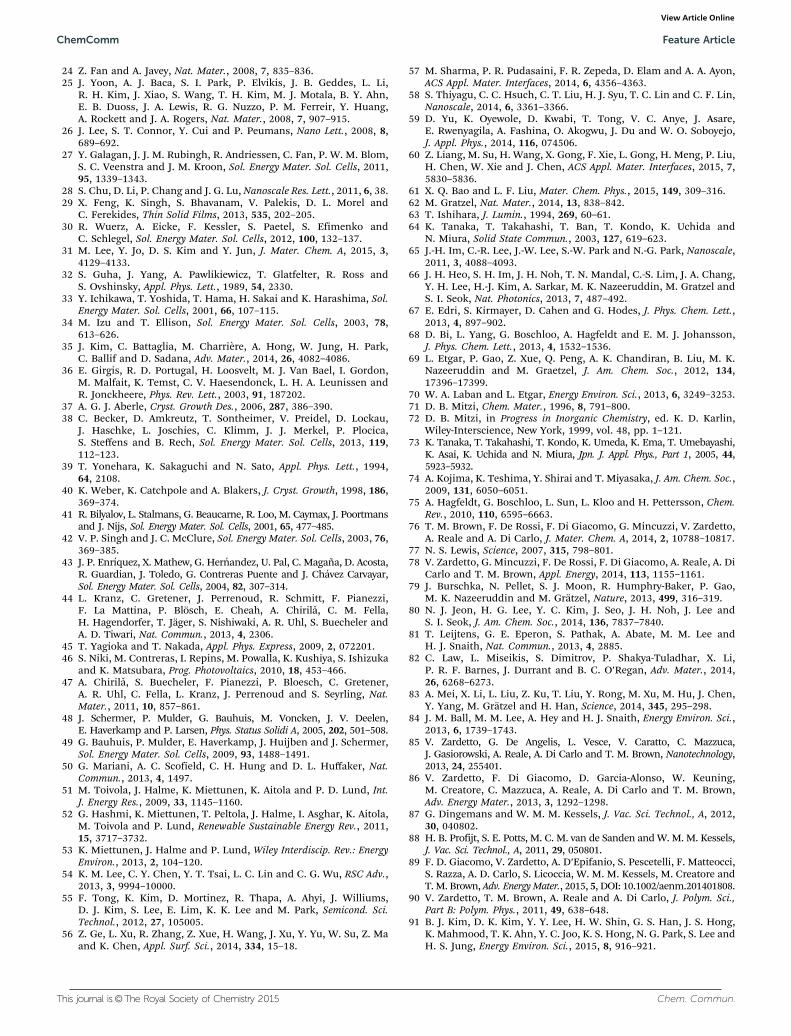
Recently, Wang et al.128 demonstrated flexible perovskite solarcells with TiO2 nanotubes coated on to Ti foil with a transparentcarbon nanotube electrode, yielding an efficiency of 8.31%. Highly-ordered TiO2 nanotube arrays were prepared by electrochemicalanodization at 20 V for 10 min at room temperature (B20 1C) andthe perovskite absorber was sequentially deposited on TiO2 nano-tube arrays. Furthermore, CNT films prepared by the chemicalvapour deposition method were coated on the perovskite absorber,which acts as a hole collector and transparent electrode. For betterhole collection, the hole transport material spiro-OMeTAD wasinfiltrated in to the CNTs network. Schematic of the devicearchitecture is shown in Fig. 16.
To observe the influence of foil thickness on the deviceflexibility, two types of Ti foils were used during cell fabrication(125 mm and 25 mm). For both thick and thin Ti-foil-basedperovskite devices, TiCl4 treatment was employed to improvethe photovoltaic performance. TiCl4 can fill the voids and cracksin the TiO2 blocking layer and therefore decrease recombinationin solar cells. Solar cells fabricated on 25 mm Ti foil exhibiteda higher photovoltage (0.83 vs. 0.70 V for non-TiCl4-treatedtubes; 0.99 vs. 0.78 V for TiCl4-treated tubes) and improved fillfactor (0.63 vs. 0.62 for non-TiCl4-treated tubes; 0.68 vs. 0.62 forTiCl4-treated tubes) compared to 125 mm Ti-foil-based solarcells. The Voc and fill factor improvement can be attributedto the smaller surface roughness of the thinner Ti foil. Thisenvisages that the smoother Ti surface improves the flatness of
Fig. 15 (a) Schematic and (b) cross-sectional SEM images of the fiber-shaped perovskite solar cell (Qiu et al. in ref. 124).
Fig. 16 (a) Schematic of a solid-state perovskite solar cell based on Tifoil/TiO2 nanotubes and carbon nanotubes and (b) image of the device(Wang et al. in ref. 128).
Table 4 Year-wise efficiency chart of flexible perovskite solar cells
YearDevicestructure
Jsc
(mA cm�2)Voc
(V) FFEfficiency(%) Ref.
7.52 0.80 0.43 2.62 Kumar et al.95
2013 14.4 0.88 0.51 6.40 Docampo99
14.30 1.04 0.47 7.00 Carmona105
14.10 0.85 0.70 8.40 Giacomo89
10.20 0.66 0.48 3.30 Qiu124
7.93 0.92 0.61 4.54 Chiang109
2014 14.36 0.99 0.68 8.30 Wang128
16.5 0.86 0.64 9.20 You101
13.40 1.03 0.73 10.20 Liu96
21.40 0.95 0.60 12.20 Kim91
9.50 0.88 0.73 6.15 Lee121
ChemComm Feature Article
View Article Online

Chem. Commun. This journal is©The Royal Society of Chemistry 2015
the perovskite layer and reduces the unfavourable series resis-tance. Thus, the thin 25 mm Ti-foil-based perovskite solar cellobtained the best PCE of 8.31%. The device also showed goodperformance after 100 mechanical bending cycles, indicatingits excellent flexibility.
Although we have discussed about the recent progress in flexibleperovskite solar cells, in Table 4 we list the annual efficienciesachieved with device architectures, for readers’ convenience.
8. Conclusions and futureperspectives
This article has reviewed recent progress in the fabricationof flexible perovskite solar cells from different approaches,including the low-temperature synthesis of TiO2 by the ALDtechnique, using ZnO as the ETL, the metal-oxide-free approachwith C60/PCBM as the ETL, and using flexible metal substrates.We observed high efficiencies (up to 12.2%) in the case ofmetal-oxide-based solar cells with good device performanceover mechanical bending, even at a low bending radius ofo1 mm as compared to metal-oxide-free devices. However,we noticed that the use of C60/PCBM as the ETL instead ofTiO2 predominantly eliminates the notorious photocurrenthysteresis and produces a PCE as high as 11.1%. Furtherimprovements in efficiency could be achieved by fine-tuningthe perovskite layer morphology by adopting slow growth andusing additives. Flexible metal-substrate-based devices alsoshowed better efficiencies of up to 8.3%, and can permithigh-temperature processes, for more effective charge collec-tion, but are limited by certain issues, including partial opacityof electrolytes and corrosion of the cheapest metallic foils.
As of now, large commercial silicon modules convert 17–25%of solar radiation into electricity, while much smaller perovskitecells in the lab scale have already reached a PCE as high as 20.1%on rigid substrates and 12.2% on flexible substrates. Fabricationcosts are also low compared to the silicon modules. Therefore,fabrication of these cells on a large scale with good efficiency isemerging and will expand the solar energy market throughoutthe world.
Long-term stability is the major issue in perovskite solarcells and restricts their outdoor photovoltaic applications. Theissues of degradation and the stability of these perovskitesshould be urgently addressed to achieve good reproducibilityand a long lifetime with high conversion efficiency. Withoutstudying the stability, one cannot transfer these exciting achieve-ments from the laboratory to industry and to outdoor applica-tions. Selecting a suitable flexible substrate also plays a majorrole in fabricating different shaped flexible devices and also toresist the mechanical bending up to extreme bending limits.Hence, extensive research is required in terms of the PCE,long-term stability, and flexibility of these devices to competewith other flexible devices to fabricate low-cost and large-areasolar panels for upcoming solar energy applications.
Acknowledgements
Authors are thankful to the CSIR-TAPSUN for financial support. Wealso gratefully acknowledge DST-UK (‘APEX’) for their support.Authors show their gratitude to all the researchers who contributedto the work cited in this article.
Notes and references1 M. A. Green, Semicond. Sci. Technol., 1993, 8, 1–12.2 J. Hupkes, B. Rech, O. Kluth, T. Repmann, J. Mullera, B. Zwaygardt,
R. Drese and M. Wuttig, Sol. Energy Mater. Sol. Cells, 2006, 90,3054–3060.
3 J. Li, H. Yu and Y. Li, Nanoscale, 2011, 3, 4888–4900.4 B. R. Huang, Y. K. Yang and W. L. Yang, Nanotechnology, 2014,
25, 035401.5 J. Britt and C. Ferekides, Appl. Phys. Lett., 1993, 62, 2851–2852.6 I. Repins, M. A. Contreras, B. Egaas, C. DeHart, J. Scharf, C. L.
Perkins, B. To and R. Noufi, Prog. Photovoltaics, 2008, 16, 235–239.7 C. W. Tang, Appl. Phys. Lett., 1986, 48, 183–185.8 B. O’Regan and M. A. Gratzel, Nature, 1991, 353, 737–740.9 J. J. M. Halls, C. A. Walsh, N. C. Greenham, E. A. Marseglia, R. H.
Friend, S. C. Moratti and A. B. Holmes, Nature, 1995, 376, 498–500.10 R. W. Miles, G. Zoppi and I. Forbes, Mater. Today, 2007, 10, 20–27.11 S. P. Singh, Ch. Pavan Kumar, G. D. Sharma, R. Kurchania and
M. S. Roy, Adv. Funct. Mater., 2012, 22, 4087–4095.12 S. P. Singh, M. S. Roy, K. R. Justin Thomas, S. Balaiah, K. Bhanuprakash
and G. D. Sharma, J. Phys. Chem. C, 2012, 116, 5941–5950.13 Q. Xue, Z. Hu, C. Sun, Z. Chen, F. Huang, H. L. Yip and Y. Cao, RSC
Adv., 2015, 5, 775–783.14 B. O’Regan, D. T. Schwartz, S. Mohammed Zakeeruddin and
M. Gratzel, Adv. Mater., 2000, 12, 1263–1267.15 H.-S. Kim, C.-R. Lee, J.-H. Im, K.-B. Lee, T. Moehl, A. Marchioro,
S.-J. Moon, R. Humphry-Baker, J.-H. Yum, J. E. Moser, M. Gratzeland N.-G. Park, Sci. Rep., 2012, 2, 591.
16 M. M. Lee, J. Teuscher, T. Miyasaka, T. N. Murakami andH. J. Snaith, Science, 2012, 338, 643–647.
17 Y. Ogomi, A. Morita, S. Tsukamoto, T. Saitho, Q. Shen, T. Toyoda,K. Yoshino, S. S. Pandey, T. Ma and S. Hayase, J. Phys. Chem. C,2014, 118, 16651–16659.
18 J. A. Christians, R. C. M. Fung and P. V. Kamat, J. Am. Chem. Soc.,2014, 136, 758–764.
19 J. Yang, A. Banerjee and S. Guha, Appl. Phys. Lett., 1997, 70, 2975.20 F. Zhang, M. Johansson, M. R. Andersson, J. C. Hummelen and
O. Inganas, Adv. Mater., 2002, 14, 662–665.21 W. U. Huynh, J. J. Dittmer and A. P. Alivisatos, Science, 2002, 295,
2425–2427.22 T. Aernouts, P. Vanlaeke, W. Geens, J. Poortmans, P. Heremans,
S. Borghs, R. Mertens, R. Andriessen and L. Leenders, Thin SolidFilms, 2004, 451, 22–25.
23 M. B. Schubert and J. H. Werner, Mater. Today, 2006, 9, 42–50.
Table 4 (continued )
YearDevicestructure
Jsc
(mA cm�2)Voc
(V) FFEfficiency(%) Ref.
2015 18.7 0.99 0.60 11.10 Ryu114
17.0 0.98 0.61 10.3 Trouihton123
Feature Article ChemComm
View Article Online
This journal is©The Royal Society of Chemistry 2015 Chem. Commun.
24 Z. Fan and A. Javey, Nat. Mater., 2008, 7, 835–836.25 J. Yoon, A. J. Baca, S. I. Park, P. Elvikis, J. B. Geddes, L. Li,
R. H. Kim, J. Xiao, S. Wang, T. H. Kim, M. J. Motala, B. Y. Ahn,E. B. Duoss, J. A. Lewis, R. G. Nuzzo, P. M. Ferreir, Y. Huang,A. Rockett and J. A. Rogers, Nat. Mater., 2008, 7, 907–915.
26 J. Lee, S. T. Connor, Y. Cui and P. Peumans, Nano Lett., 2008, 8,689–692.
27 Y. Galagan, J. J. M. Rubingh, R. Andriessen, C. Fan, P. W. M. Blom,S. C. Veenstra and J. M. Kroon, Sol. Energy Mater. Sol. Cells, 2011,95, 1339–1343.
28 S. Chu, D. Li, P. Chang and J. G. Lu, Nanoscale Res. Lett., 2011, 6, 38.29 X. Feng, K. Singh, S. Bhavanam, V. Palekis, D. L. Morel and
C. Ferekides, Thin Solid Films, 2013, 535, 202–205.30 R. Wuerz, A. Eicke, F. Kessler, S. Paetel, S. Efimenko and
C. Schlegel, Sol. Energy Mater. Sol. Cells, 2012, 100, 132–137.31 M. Lee, Y. Jo, D. S. Kim and Y. Jun, J. Mater. Chem. A, 2015, 3,
4129–4133.32 S. Guha, J. Yang, A. Pawlikiewicz, T. Glatfelter, R. Ross and
S. Ovshinsky, Appl. Phys. Lett., 1989, 54, 2330.33 Y. Ichikawa, T. Yoshida, T. Hama, H. Sakai and K. Harashima, Sol.
Energy Mater. Sol. Cells, 2001, 66, 107–115.34 M. Izu and T. Ellison, Sol. Energy Mater. Sol. Cells, 2003, 78,
613–626.35 J. Kim, C. Battaglia, M. Charriere, A. Hong, W. Jung, H. Park,
C. Ballif and D. Sadana, Adv. Mater., 2014, 26, 4082–4086.36 E. Girgis, R. D. Portugal, H. Loosvelt, M. J. Van Bael, I. Gordon,
M. Malfait, K. Temst, C. V. Haesendonck, L. H. A. Leunissen andR. Jonckheere, Phys. Rev. Lett., 2003, 91, 187202.
37 A. G. J. Aberle, Cryst. Growth Des., 2006, 287, 386–390.38 C. Becker, D. Amkreutz, T. Sontheimer, V. Preidel, D. Lockau,
J. Haschke, L. Joschies, C. Klimm, J. J. Merkel, P. Plocica,S. Steffens and B. Rech, Sol. Energy Mater. Sol. Cells, 2013, 119,112–123.
39 T. Yonehara, K. Sakaguchi and N. Sato, Appl. Phys. Lett., 1994,64, 2108.
40 K. Weber, K. Catchpole and A. Blakers, J. Cryst. Growth, 1998, 186,369–374.
41 R. Bilyalov, L. Stalmans, G. Beaucarne, R. Loo, M. Caymax, J. Poortmansand J. Nijs, Sol. Energy Mater. Sol. Cells, 2001, 65, 477–485.
42 V. P. Singh and J. C. McClure, Sol. Energy Mater. Sol. Cells, 2003, 76,369–385.
43 J. P. Enrıquez, X. Mathew, G. Hernandez, U. Pal, C. Magana, D. Acosta,R. Guardian, J. Toledo, G. Contreras Puente and J. Chavez Carvayar,Sol. Energy Mater. Sol. Cells, 2004, 82, 307–314.
44 L. Kranz, C. Gretener, J. Perrenoud, R. Schmitt, F. Pianezzi,F. La Mattina, P. Blosch, E. Cheah, A. Chirila, C. M. Fella,H. Hagendorfer, T. Jager, S. Nishiwaki, A. R. Uhl, S. Buecheler andA. D. Tiwari, Nat. Commun., 2013, 4, 2306.
45 T. Yagioka and T. Nakada, Appl. Phys. Express, 2009, 2, 072201.46 S. Niki, M. Contreras, I. Repins, M. Powalla, K. Kushiya, S. Ishizuka
and K. Matsubara, Prog. Photovoltaics, 2010, 18, 453–466.47 A. Chirila, S. Buecheler, F. Pianezzi, P. Bloesch, C. Gretener,
A. R. Uhl, C. Fella, L. Kranz, J. Perrenoud and S. Seyrling, Nat.Mater., 2011, 10, 857–861.
48 J. Schermer, P. Mulder, G. Bauhuis, M. Voncken, J. V. Deelen,E. Haverkamp and P. Larsen, Phys. Status Solidi A, 2005, 202, 501–508.
49 G. Bauhuis, P. Mulder, E. Haverkamp, J. Huijben and J. Schermer,Sol. Energy Mater. Sol. Cells, 2009, 93, 1488–1491.
50 G. Mariani, A. C. Scofield, C. H. Hung and D. L. Huffaker, Nat.Commun., 2013, 4, 1497.
51 M. Toivola, J. Halme, K. Miettunen, K. Aitola and P. D. Lund, Int.J. Energy Res., 2009, 33, 1145–1160.
52 G. Hashmi, K. Miettunen, T. Peltola, J. Halme, I. Asghar, K. Aitola,M. Toivola and P. Lund, Renewable Sustainable Energy Rev., 2011,15, 3717–3732.
53 K. Miettunen, J. Halme and P. Lund, Wiley Interdiscip. Rev.: EnergyEnviron., 2013, 2, 104–120.
54 K. M. Lee, C. Y. Chen, Y. T. Tsai, L. C. Lin and C. G. Wu, RSC Adv.,2013, 3, 9994–10000.
55 F. Tong, K. Kim, D. Mortinez, R. Thapa, A. Ahyi, J. Williums,D. J. Kim, S. Lee, E. Lim, K. K. Lee and M. Park, Semicond. Sci.Technol., 2012, 27, 105005.
56 Z. Ge, L. Xu, R. Zhang, Z. Xue, H. Wang, J. Xu, Y. Yu, W. Su, Z. Maand K. Chen, Appl. Surf. Sci., 2014, 334, 15–18.
57 M. Sharma, P. R. Pudasaini, F. R. Zepeda, D. Elam and A. A. Ayon,ACS Appl. Mater. Interfaces, 2014, 6, 4356–4363.
58 S. Thiyagu, C. C. Hsuch, C. T. Liu, H. J. Syu, T. C. Lin and C. F. Lin,Nanoscale, 2014, 6, 3361–3366.
59 D. Yu, K. Oyewole, D. Kwabi, T. Tong, V. C. Anye, J. Asare,E. Rwenyagila, A. Fashina, O. Akogwu, J. Du and W. O. Soboyejo,J. Appl. Phys., 2014, 116, 074506.
60 Z. Liang, M. Su, H. Wang, X. Gong, F. Xie, L. Gong, H. Meng, P. Liu,H. Chen, W. Xie and J. Chen, ACS Appl. Mater. Interfaces, 2015, 7,5830–5836.
61 X. Q. Bao and L. F. Liu, Mater. Chem. Phys., 2015, 149, 309–316.62 M. Gratzel, Nat. Mater., 2014, 13, 838–842.63 T. Ishihara, J. Lumin., 1994, 269, 60–61.64 K. Tanaka, T. Takahashi, T. Ban, T. Kondo, K. Uchida and
N. Miura, Solid State Commun., 2003, 127, 619–623.65 J.-H. Im, C.-R. Lee, J.-W. Lee, S.-W. Park and N.-G. Park, Nanoscale,
2011, 3, 4088–4093.66 J. H. Heo, S. H. Im, J. H. Noh, T. N. Mandal, C.-S. Lim, J. A. Chang,
Y. H. Lee, H.-J. Kim, A. Sarkar, M. K. Nazeeruddin, M. Gratzel andS. I. Seok, Nat. Photonics, 2013, 7, 487–492.
67 E. Edri, S. Kirmayer, D. Cahen and G. Hodes, J. Phys. Chem. Lett.,2013, 4, 897–902.
68 D. Bi, L. Yang, G. Boschloo, A. Hagfeldt and E. M. J. Johansson,J. Phys. Chem. Lett., 2013, 4, 1532–1536.
69 L. Etgar, P. Gao, Z. Xue, Q. Peng, A. K. Chandiran, B. Liu, M. K.Nazeeruddin and M. Graetzel, J. Am. Chem. Soc., 2012, 134,17396–17399.
70 W. A. Laban and L. Etgar, Energy Environ. Sci., 2013, 6, 3249–3253.71 D. B. Mitzi, Chem. Mater., 1996, 8, 791–800.72 D. B. Mitzi, in Progress in Inorganic Chemistry, ed. K. D. Karlin,
Wiley-Interscience, New York, 1999, vol. 48, pp. 1–121.73 K. Tanaka, T. Takahashi, T. Kondo, K. Umeda, K. Ema, T. Umebayashi,
K. Asai, K. Uchida and N. Miura, Jpn. J. Appl. Phys., Part 1, 2005, 44,5923–5932.
74 A. Kojima, K. Teshima, Y. Shirai and T. Miyasaka, J. Am. Chem. Soc.,2009, 131, 6050–6051.
75 A. Hagfeldt, G. Boschloo, L. Sun, L. Kloo and H. Pettersson, Chem.Rev., 2010, 110, 6595–6663.
76 T. M. Brown, F. De Rossi, F. Di Giacomo, G. Mincuzzi, V. Zardetto,A. Reale and A. Di Carlo, J. Mater. Chem. A, 2014, 2, 10788–10817.
77 N. S. Lewis, Science, 2007, 315, 798–801.78 V. Zardetto, G. Mincuzzi, F. De Rossi, F. Di Giacomo, A. Reale, A. Di
Carlo and T. M. Brown, Appl. Energy, 2014, 113, 1155–1161.79 J. Burschka, N. Pellet, S. J. Moon, R. Humphry-Baker, P. Gao,
M. K. Nazeeruddin and M. Gratzel, Nature, 2013, 499, 316–319.80 N. J. Jeon, H. G. Lee, Y. C. Kim, J. Seo, J. H. Noh, J. Lee and
S. I. Seok, J. Am. Chem. Soc., 2014, 136, 7837–7840.81 T. Leijtens, G. E. Eperon, S. Pathak, A. Abate, M. M. Lee and
H. J. Snaith, Nat. Commun., 2013, 4, 2885.82 C. Law, L. Miseikis, S. Dimitrov, P. Shakya-Tuladhar, X. Li,
P. R. F. Barnes, J. Durrant and B. C. O’Regan, Adv. Mater., 2014,26, 6268–6273.
83 A. Mei, X. Li, L. Liu, Z. Ku, T. Liu, Y. Rong, M. Xu, M. Hu, J. Chen,Y. Yang, M. Gratzel and H. Han, Science, 2014, 345, 295–298.
84 J. M. Ball, M. M. Lee, A. Hey and H. J. Snaith, Energy Environ. Sci.,2013, 6, 1739–1743.
85 V. Zardetto, G. De Angelis, L. Vesce, V. Caratto, C. Mazzuca,J. Gasiorowski, A. Reale, A. Di Carlo and T. M. Brown, Nanotechnology,2013, 24, 255401.
86 V. Zardetto, F. Di Giacomo, D. Garcia-Alonso, W. Keuning,M. Creatore, C. Mazzuca, A. Reale, A. Di Carlo and T. M. Brown,Adv. Energy Mater., 2013, 3, 1292–1298.
87 G. Dingemans and W. M. M. Kessels, J. Vac. Sci. Technol., A, 2012,30, 040802.
88 H. B. Profijt, S. E. Potts, M. C. M. van de Sanden and W. M. M. Kessels,J. Vac. Sci. Technol., A, 2011, 29, 050801.
89 F. D. Giacomo, V. Zardetto, A. D’Epifanio, S. Pescetelli, F. Matteocci,S. Razza, A. D. Carlo, S. Licoccia, W. M. M. Kessels, M. Creatore andT. M. Brown, Adv. Energy Mater., 2015, 5, DOI: 10.1002/aenm.201401808.
90 V. Zardetto, T. M. Brown, A. Reale and A. Di Carlo, J. Polym. Sci.,Part B: Polym. Phys., 2011, 49, 638–648.
91 B. J. Kim, D. K. Kim, Y. Y. Lee, H. W. Shin, G. S. Han, J. S. Hong,K. Mahmood, T. K. Ahn, Y. C. Joo, K. S. Hong, N. G. Park, S. Lee andH. S. Jung, Energy Environ. Sci., 2015, 8, 916–921.
ChemComm Feature Article
View Article Online

Chem. Commun. This journal is©The Royal Society of Chemistry 2015
92 Q. Zhang, C. S. Dandeneau, X. Zhou and C. Cao, Adv. Mater., 2009,21, 4087–4108.
93 J. B. Baxter and E. S. Aydil, Appl. Phys. Lett., 2005, 86, 1–3.94 I. Gonzalez-Valls and M. Lira-Cantu, Energy Environ. Sci., 2009, 2,
19–34.95 M. H. Kumar, N. Yantara, S. Dharani, M. Graetzel, S. Mhaisalkar,
P. P. Boix and N. Mathews, Chem. Commun., 2013, 49, 11089–11091.96 D. Liu and T. L. Kelly, Nat. Photonics, 2014, 8, 133–138.97 J. Y. Jeng, Y. F. Chiang, M. H. Lee, S. R. Peng, T. F. Guo, P. Chen
and T. C. Wen, Adv. Mater., 2013, 25, 3727–3732.98 S. Y. Sun, T. Salim, N. Mathews, M. Duchamp, C. Boothroyd,
G. Xing, T. C. Sum and Y. M. Lam, Energy Environ. Sci., 2014, 7,399–407.
99 P. Docampo, J. M. Ball, M. Darwich, G. E. Eperon and H. J. Snaith,Nat. Commun., 2013, 4, 2761–2766.
100 O. Malinkiewicz, A. Yella, Y. H. Lee, G. M. Espallargas, M. Graetzel,M. K. Nazeeruddin and H. J. Bolink, Nat. Photonics, 2014, 8,133–138.
101 J. You, Z. Hong, Y. M. Yang, Q. Chen, M. Cai, T.-B. Song,C.-C. Chen, S. Lu, Y. Liu, H. Zhou and Y. Yang, ACS Nano, 2014,8, 1674–1680.
102 J. Seo, S. Park, Y. C. Kim, N. J. Nam, J. H. Noh, S. C. Yoon andS. I. Seok, Energy Environ. Sci., 2014, 7, 2642–2646.
103 Q. Wang, Y. Shao, Q. Dong, Z. Xiao, Y. Yuan and J. Huang, EnergyEnviron. Sci., 2014, 7, 2359–2365.
104 Z. Xiao, Q. Dong, C. Bi, Y. Shao, Y. Yuan and J. Huang, Adv. Mater.,2014, 26, 6503–6509.
105 C. R. Carmona, O. Malinkiewicz, A. Soriano, G. M. Espallargas,A. Garcia, P. Reinecke, T. Kroyer, M. I. Dar, M. K. Nazeeruddineand H. J. Bolink, Energy Environ. Sci., 2014, 7, 994–997.
106 Z. He, C. Zhong, S. Su, M. Xu, H. Wu and Y. Cao, Nat. Photonics,2012, 6, 591–595.
107 Z. He, C. Zhong, X. Huang, W. Y. Wong, H. Wu, L. Chen, S. Su andY. Cao, Adv. Mater., 2011, 23, 4636–4643.
108 S. D. Stranks, G. E. Eperon, G. Grancini, C. Menelaou,M. J. P. Alcocer, T. Leijtens, L. M. Herz, A. Petrozza andH. J. Snaith, Science, 2013, 342, 341–344.
109 Y. F. Chiang, J. Y. Jeng, M. H. Lee, S. R. Peng, P. Chen, T. F. Guo,T. C. Wen, Y. J. Hsu and C. M. Hsu, Phys. Chem. Chem. Phys., 2014,16, 6033–6040.
110 J. Seo, S. Park, Y. C. Kim, N. J. Jeon, Y. H. Noh, S. C. Yoon andS. I. Seok, Chem. Rev., 2014, 114, 1973–2129.
111 Y. Shao, Z. Xiao, C. Bi, Y. Yuan and J. Huang, Nat. Commun., 2014,5, 5784.
112 Q. Xue, Z. Hu, Y. Liu, J. Lin, C. Sun, Z. Chen, C. Duan, J. Wang,C. Liao, W. M. Lau, F. Huang, H. L. Yip and Y. Cao, J. Mater. Chem.A, 2014, 2, 19598–19603.
113 M. Jorgensen, K. Norman and F. C. Krebs, Sol. Energy Mater. Sol.Cells, 2008, 92, 686–714.
114 S. Ryu, J. Seo, S. S. Shin, Y. C. Kim, N. J. Jeon, J. H. Noh and S. IlSeok, J. Mater. Chem. A, 2015, 3, 3271–3275.
115 Y. Zhou, C. F. Hernandez, J. Shim, J. Meyer, A. J. Giordano, H. Li,P. Winget, T. Papadopoulos, H. Cheun, J. Im, M. Fenoll, A. Dindar,W. Haske, E. Najafabadi, T. M. Khan, H. Sojoudi, S. Barlow,S. Graham, J. Bredas, S. R. Marder, A. Kahn and B. Kippelen,Science, 2012, 336, 327–332.
116 H. Kang, S. Hong, J. Lee and K. Lee, Adv. Mater., 2014, 24,3005–3009.
117 S. I. Na, S. S. Kim, J. Jo and D. Y. Kim, Adv. Mater., 2008, 20,4061–4067.
118 A. Kim, Y. Won, K. Woo, S. Jeong and J. Moon, Adv. Funct. Mater.,2014, 24, 2462–2471.
119 W. Wang, Q. Zhao, H. Li, H. Wu, D. Zou and D. Yu, Adv. Funct.Mater., 2012, 22, 2775–2782.
120 S. K. Balasingam, M. G. Kang and Y. Jun, Chem. Commun., 2013, 49,11457–11475.
121 M. Lee, Y. Jo, D. S. Kim and Y. Jun, J. Mater. Chem. A, 2015, 3,4129–4133.
122 L. Zuo, C. C. Chueh, Y. X. Xu, K. S. Chen, Y. Zang, C. Z. Li, H. Chenand A. K. Y. Jen, Adv. Mater., 2014, 26, 6778–6784.
123 J. Troughton, D. Bryant, K. Wojciechowski, M. J. Carnie, H. Snaith,D. A. Worsley and T. M. Watson, J. Mater. Chem. A, 2015, 3,9141–9145.
124 L. Qiu, J. Deng, X. Lu, Z. Yang and H. Peng, Angew. Chem., Int. Ed.,2014, 53, 10425–10428.
125 H. Sun, H. Li, X. You, Z. Yang, J. Deng, L. Qiu and H. Peng, J. Mater.Chem. A, 2014, 2, 345–349.
126 D. Liu, M. Zhao, Y. Li, Z. Bian, L. Zhang, Y. Shang, X. Xia, S. Zhang,D. Yun, Z. Liu, A. Cao and C. Huang, ACS Nano, 2012, 6,11027–11034.
127 Z. Zhang, X. Chen, P. Chen, G. Guan, L. Qiu, H. Lin, Z. Yang,W. Bai, Y. Luo and H. Peng, Adv. Mater., 2014, 26, 466–470.
128 X. Wang, Z. Li, W. Xu, S. A. Kulkarni, S. K. Batabyal, S. Zhang,A. Cao and L. H. Wong, Nano Energy, 2015, 11, 728–735.
Feature Article ChemComm
View Article Online