Realization of Different Multiplexers by Using COG ... · International Realization of Different...
7
Realization of Different Multiplexers by Using COG Reversible Gate S. Mamataj ECE Department, Murshidabad College of Engineering and Technology, Berhampore, WB, India Email: [email protected] B. Das CSE Department, Murshidabad College of Engineering and Technology, Berhampore, WB, India Email: [email protected] A. Rahaman AEIE Department, Future Institute of Engineering and Technology, Sonarpur, WB, India Email: [email protected] Abstract—Reversible logic is one of the most essential issues at present time due to its power reduction capability in circuit designing. It finds application in various fields including quantum computing, optical computing, nanotechnology, computer graphic, cryptography, digital signal processing and many more. Dissipation of a significant amount of energy is achieved in the conventional digital circuits because bits of information are erased during the logic operations. Thus, if logic gates are designed in such a way that the information bits are not destroyed, then it is possible to reduce the power consumption dramatically. The information bits are not lost in case of a reversible computation. This has led to the development of reversible gates. The reversible circuits do not lose information and can generate unique outputs from the specified inputs and vice versa. The main purposes of designing reversible logic are to decrease quantum cost, depth of the circuits and the number of garbage outputs. This paper represents the realization of different multiplexers by using COG reversible gate and a comparison of cost metrics of different multiplexers. Also the COG gate and multiplexer by this COG gate have been simulated by XILINX and implemented in the SPARTAN-FPGA Kit. Index Terms—basic reversible gates, reversible multiplexer, irreversible multiplexer, garbage output, constant input, technology, select lines I. INTRODUCTION Modern digital circuits offer a great deal of computation. As technology evolves and many more transistors can fit in a given area, the concern for power dissipation as heat arises. Reversible logic was first related to energy when in 1973. It was Landauer states that information loss due to function irreversibility leads to energy dissipation in 1961 who stated that there is small amount of heat dissipation the circuit due to loss of Manuscript received February11, 2014; revised October 22, 2014. where ‘k’ is Boltzmann constant and T is the absolute temperature [1]. This principle is further supported by Bennett that zero energy dissipation can be achieved only when the circuit contains reversible gates. Bennett showed that the energy would not be dissipating from the circuit if inputs can be extracted from outputs and it would be possible if and only if reversible gates are used in the circuits [2]. According to Moore’s law the numbers of transistors will double every 18 months. Thus energy conservative devices are the prime need at the end of the day. The amount of energy dissipated in a system bears a direct relationship to the number of bits erased during computation. Reversible circuits are those circuits that do not lose information. A circuit will be reversible if input vectors can be explicitly retrieved from output vectors and one to one correspondence are there between inputs and outputs [3]. Younis and Knight [4] showed that some reversible circuits can be made asymptotically energy- lossless if their delay is allowed to be arbitrarily large. A reversible logic circuit should have the following features [5], use of minimum number of reversible gates, use of minimum number of garbage outputs and use of minimum constant inputs. II. REVERSIBLE LOGIC A. Definitions Some of the basic definitions [6] pertaining to Reversible Logic are Definition 1: Reversible logic function A reversible logic function is a function which maps each input vector to a unique output vector. A function is said reversible if, from its given output, it is always possible to determine back its input, because there is a one-to-one relationship between input and output states. Definition 2: Reversible logic gate A reversible logic gate is a device which performs reversible computation maintaining one to one mapping between the inputs and outputs. If a reversible logic gate International Journal of Electronics and Electrical Engineering Vol. 3, No. 5, October 2015 ©2015 Engineering and Technology Publishing 365 10.12720/ijeee.3.5.365-371 doi: one bit of information and it would be equal to kTln2,
Transcript of Realization of Different Multiplexers by Using COG ... · International Realization of Different...

Realization of Different Multiplexers by Using
COG Reversible Gate
S. Mamataj ECE Department, Murshidabad College of Engineering and Technology, Berhampore, WB, India
Email: [email protected]
B. Das CSE Department, Murshidabad College of Engineering and Technology, Berhampore, WB, India
Email: [email protected]
A. Rahaman AEIE Department, Future Institute of Engineering and Technology, Sonarpur, WB, India
Email: [email protected]
Abstract—Reversible logic is one of the most essential issues
at present time due to its power reduction capability in
circuit designing. It finds application in various fields
including quantum computing, optical computing,
nanotechnology, computer graphic, cryptography, digital
signal processing and many more. Dissipation of a
significant amount of energy is achieved in the conventional
digital circuits because bits of information are erased during
the logic operations. Thus, if logic gates are designed in such
a way that the information bits are not destroyed, then it is
possible to reduce the power consumption dramatically. The
information bits are not lost in case of a reversible
computation. This has led to the development of reversible
gates. The reversible circuits do not lose information and
can generate unique outputs from the specified inputs and
vice versa. The main purposes of designing reversible logic
are to decrease quantum cost, depth of the circuits and the
number of garbage outputs. This paper represents the
realization of different multiplexers by using COG
reversible gate and a comparison of cost metrics of different
multiplexers. Also the COG gate and multiplexer by this
COG gate have been simulated by XILINX and
implemented in the SPARTAN-FPGA Kit.
Index Terms—basic reversible gates, reversible multiplexer,
irreversible multiplexer, garbage output, constant input,
technology, select lines
I. INTRODUCTION
Modern digital circuits offer a great deal of
computation. As technology evolves and many more
transistors can fit in a given area, the concern for power
dissipation as heat arises. Reversible logic was first
related to energy when in 1973. It was Landauer states
that information loss due to function irreversibility leads
to energy dissipation in 1961 who stated that there is
small amount of heat dissipation the circuit due to loss of
Manuscript received February11, 2014; revised October 22, 2014.
where ‘k’ is Boltzmann constant and T is the absolute
temperature [1]. This principle is further supported by
Bennett that zero energy dissipation can be achieved only
when the circuit contains reversible gates. Bennett
showed that the energy would not be dissipating from the
circuit if inputs can be extracted from outputs and it
would be possible if and only if reversible gates are used
in the circuits [2]. According to Moore’s law the numbers
of transistors will double every 18 months. Thus energy
conservative devices are the prime need at the end of the
day. The amount of energy dissipated in a system bears a
direct relationship to the number of bits erased during
computation. Reversible circuits are those circuits that do
not lose information. A circuit will be reversible if input
vectors can be explicitly retrieved from output vectors
and one to one correspondence are there between inputs
and outputs [3]. Younis and Knight [4] showed that some
reversible circuits can be made asymptotically energy-
lossless if their delay is allowed to be arbitrarily large. A
reversible logic circuit should have the following features
[5], use of minimum number of reversible gates, use of
minimum number of garbage outputs and use of
minimum constant inputs.
II. REVERSIBLE LOGIC
A. Definitions
Some of the basic definitions [6] pertaining to
Reversible Logic are
Definition 1: Reversible logic function A reversible logic function is a function which maps
each input vector to a unique output vector. A function is
said reversible if, from its given output, it is always
possible to determine back its input, because there is a
one-to-one relationship between input and output states.
Definition 2: Reversible logic gate
A reversible logic gate is a device which performs
reversible computation maintaining one to one mapping
between the inputs and outputs. If a reversible logic gate
International Journal of Electronics and Electrical Engineering Vol. 3, No. 5, October 2015
©2015 Engineering and Technology Publishing 36510.12720/ijeee.3.5.365-371doi:
one bit of information and it would be equal to kTln2,
has N inputs, then to perform one to one mapping, the
number of outputs should also be N. Then this device
may be called an NxN reversible logic gate whose inputs
are denoted by I1 I2 I3…IN and the outputs are denoted by
O1O2 O3…ON.
Definition 3: Garbage output
These are the outputs that are not used in the synthesis
of a function. These may appear to be redundant but are
very essential to preserve the reversibility of a gate. It is
denoted by GO.
Definition 4: Constant inputs
These are the inputs that have to be maintained at
either a constant 0 or at constant 1 in order to generate a
given logical expression by using the reversible logic
gates. It is abbreviated as CI.
Definition 5: Quantum cost
This refers to the cost of the circuit in terms of the cost
of a primitive gate. It is computed knowing the number of
primitive reversible logic gates (1×1 or 2×2) required to
realize the circuit. It is denoted as QC.
Definition 6: Gate count
This refers to the number of gates that are required to
implement a reversible logic circuit. It is denoted by GC.
Another parameter that can be defined in relation to the
gate count is the flexibility, which can be defined as the
ability of a reversible logic gate in realizing more
functions. Higher the flexibility of a gate, lesser is the
number of gates that are needed to implement a given
function.
Definition 7: Hardware complexity
The hardware complexity [7] is measured by counting
the number of EX-OR operations, number of AND
operations and number of NOT operations. Let
α = No. of EX-OR operations
β = No. of AND operations
δ = No. of NOT operations
Then the total hardware complexity is given as sum of
EX-OR, AND and NOT operations.
Figure 1. Basic reversible gates.
B. Reversible Logic Gates
The important basic reversible logic gate is Feynman
gate [8] which is the only 2×2 reversible gate and it is
used most popularly by the designers for fan-out purposes.
There is also a double Feynman gate [9], Fredkin gate [10]
and Toffoli gate [11], New Gate [12], Peres gate [13], all
of which can be used to realize important combinational
functions and all are 3×3 reversible gates. Some basic
reversible gates are shown in Fig. 1.
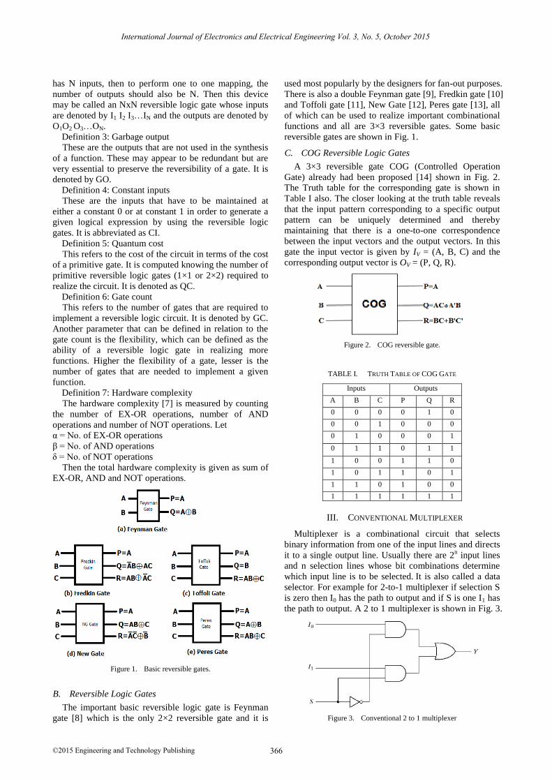
C. COG Reversible Logic Gates
A 3×3 reversible gate COG (Controlled Operation
Gate) already had been proposed [14] shown in Fig. 2.
The Truth table for the corresponding gate is shown in
Table I also. The closer looking at the truth table reveals
that the input pattern corresponding to a specific output
pattern can be uniquely determined and thereby
maintaining that there is a one-to-one correspondence
between the input vectors and the output vectors. In this
III. CONVENTIONAL MULTIPLEXER
Multiplexer is a combinational circuit that selects
binary information from one of the input lines and directs
it to a single output line. Usually there are 2n input lines
and n selection lines whose bit combinations determine
which input line is to be selected. It is also called a data
selector. For example for 2-to-1 multiplexer if selection S
is zero then I0 has the path to output and if S is one I1 has
the path to output. A 2 to 1 multiplexer is shown in Fig. 3.
Figure 3. Conventional 2 to 1 multiplexer
International Journal of Electronics and Electrical Engineering Vol. 3, No. 5, October 2015
©2015 Engineering and Technology Publishing 366
TABLE I. TRUTH TABLE OF COG GATE
Inputs Outputs
A B C P Q R
0 0 0 0 1 0
0 0 1 0 0 0
0 1 0 0 0 1
0 1 1 0 1 1
1 0 0 1 1 0
1 0 1 1 0 1
1 1 0 1 0 0
1 1 1 1 1 1
gate the input vector is given by IV = (A, B, C) and the
corresponding output vector is OV = (P, Q, R).
Figure 2. COG reversible gate.

Figure 4. Conventional 4 to 1 multiplexer
Larger multiplexers can be constructed by using
smaller multiplexers by chaining them together. For
example, an 8-to-1 multiplexer can be made with two 4-
to-1 and one 2-to-1 multiplexers. The two 4-to-1
multiplexer outputs are fed into the 2-to-1 with the
selector pins on the 4-to-1's put in parallel giving a total
number of selector inputs to 3, which is equivalent to an
8-to-1. An 8 to 1 multiplexer of basic gate is shown in Fig.
5.
Figure 5. Conventional 8 to 1 multiplexer
IV. REALIZATION OF MULTIPLEXER BY COG GATE
Different types of multiplexer have been realized in
this paper by using COG reversible gates.
Using the reversible COG gate, 4:1 multiplexer can
also be designed as shown in Fig. 7. This design requires
three COG gates such that producing four garbage
outputs. The Table III describes the truth table of 4:1
reversible multiplexer, the garbage outputs are discarded
as it doesn’t play a vital role in the multiplexing operation.
Figure 7. Reversible 4 to 1 multiplexer
International Journal of Electronics and Electrical Engineering Vol. 3, No. 5, October 2015
©2015 Engineering and Technology Publishing 367
A 2-to-1 multiplexer has a Boolean equation
Y=S’I0+SI1, where I0 and I1 are the two inputs, S is the
selector input, and Y is the output which can be expressed
as a truth table shown in Table II.
TABLE II. TRUTH TABLE OF 2 TO 1 MULTIPLEXER
S I0 I1 Y
0
1 1 1
0 1
0 1 0
0 0
1
1
1 1
0 0
0 1 1
0 0
This truth table shows that when S=0 then Y=I0 but
when S=1 then Y=I1. A straightforward realization of this
2-to-1 multiplexer would need 2 AND gates, an OR gate,
and a NOT gate.
Larger multiplexers are also common and, as stated
above, require log2 (n) selector pins for n inputs. Other
common sizes are 4-to-1, 8-to-1, and 16-to-1. Since
digital logic uses binary values, powers of 2 are used (4, 8,
and 16) to maximally control a number of inputs for the
given number of selector inputs.
The Boolean equation for a 4-to-1 multiplexer is
Y=I0S0’S1’+I1S0S1’+I2S0’S1+I3S0S1, where I0, I1, I2 and I3
are the two inputs, S is the selector input, and Y is the
output A 4 to 1 multiplexer is shown in Fig. 4.
A. Design of 2:1 Reversible Multiplexer Using COG
Gate
The 3×3 reversible COG gate is used in order to act as
the 2:1 reversible multiplexer producing two garbage bits
shown in Fig. 6. The inputs are S0, I0 and I1. Based on the
selection input S0, the corresponding message bits are
passed on to the output Y.
Figure 6. Reversible 2 to 1 multiplexer
B. Design of 4:1 Reversible Multiplexer Using COG
Gate

TABLE III. TRUTH TABLE OF 4 TO 1 MULTIPLEXER
S1 S0 Y
0 0 I0
0 1 I1
1 0 I2
1 1 I3
The above truth table depicts there is no change in the
functionality of 4:1 reversible multiplexer with respect to
the irreversible multiplexer functionality. The equation
for the output Y is given as follows,
Figure 8. Reversible 8 to 1 multiplexer
Figure 9. Reversible 16 to 1 multiplexer
C. Design of 8:1 and 16:1Reversible Multiplexer Using
Reversible COG Gate
Using the same proposed COG gate again 8:1 and 16:1
reversible multiplexer also can be designed as shown in
Fig. 8 and Fig. 9. These designs use seven and fifteen
COG gates producing 10 and 19 garbage outputs
respectively. In genera designing of 2n:1 reversible
multiplexer can be possible where n is 1, 2, 3…n. For
2n:1 reversible multiplexer (2
n-1) COG gates are required
producing (2n+n-1) number of garbage outputs
V. COMPARISON
TABLE IV. COMPARISON OF COST METRICS OF DIFFERENT
MULTIPLEXERS
[Proposed]
MUX GC GO T
2:1
1 2 2 α+2ß+2δ
4:1
3 5 6 α+6ß+6δ
8:1 7 10 14 α+14ß+14δ
16:1 15 19 30 α+30ß+30δ
2n:1 (2n-1) (2n+n-1) (2n-1) (2 α+2ß+2δ)
TABLE V. COMPARISON OF DIFFERENT CONVENTIONAL AND
REVERSIBLE MULTIPLEXERS
MUX
No of gates
Reversible MUX
[proposed]
Irreversible
MUX
2:1
1 4
4:1
3 7
8:1 7 12
16:1 15 21
2n:1 (2n-1) (2n+n+1)
TABLE VI. COMPARISON OF DIFFERENT 4:1 REVERSIBLE
MULTIPLEXERS
Name of the circuit
No of gates
Garbage output
Constant Input
hardware Complexity
4:1 MUX
[15]
6 10 4 11α+10ß+2δ
4:1 MUX [16]
3 6 0 6α+8ß+3δ
4:1 MUX
[17]
3 5 0 6α+12β+6δ
4:1 MUX
[proposed]
3 5 0 6 α+6ß+6δ
VI. SIMULATION RESULTS
This work also includes the simulation of the COG
gate and multiplexer using this proposed gate. The
simulated snapshot input, output waveforms and RTL
schematics of the proposed circuits are shown from Fig.
10 to Fig. 21. The simulation has been done by XILINX
ISE 8.2 and also the implementation in the SPARTAN-3
FPGA kit has been achieved.
The VHDL program for COG gate
---------------------------------------------------------------------
entity COG_gate_vhdl is
Port (A: in STD_LOGIC;
B: in STD_LOGIC;
C: in STD_LOGIC;
P: out STD_LOGIC;
Q: out STD_LOGIC;
R: out STD_LOGIC);
International Journal of Electronics and Electrical Engineering Vol. 3, No. 5, October 2015
©2015 Engineering and Technology Publishing 368
Y=I0S0’S1’+I1S0S1’+I2S0’S1+I3S0S1.
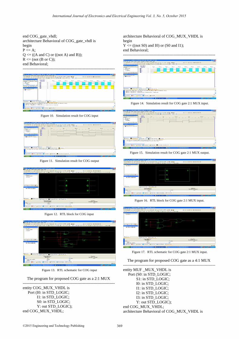
end COG_gate_vhdl;
architecture Behavioral of COG_gate_vhdl is
begin
P <= A;
Q <= ((A and C) or ((not A) and B));
R <= (not (B or C));
end Behavioral;
---------------------------------------------------------------------
Figure 10. Simulation result for COG input
Figure 11. Simulation result for COG output
Figure 12. RTL block for COG input
Figure 13. RTL schematic for COG input
The program for proposed COG gate as a 2:1 MUX
---------------------------------------------------------------------
entity COG_MUX_VHDL is
Port (I0: in STD_LOGIC;
I1: in STD_LOGIC;
S0: in STD_LOGIC;
Y: out STD_LOGIC);
end COG_MUX_VHDL;
architecture Behavioral of COG_MUX_VHDL is
begin
Y <= ((not S0) and I0) or (S0 and I1);
end Behavioral;
---------------------------------------------------------------------
Figure 14. Simulation result for COG gate 2:1 MUX input.
Figure 15. Simulation result for COG gate 2:1 MUX output.
Figure 16. RTL block for COG gate 2:1 MUX input.
Figure 17. RTL schematic for COG gate 2:1 MUX input.
The program for proposed COG gate as a 4:1 MUX
---------------------------------------------------------------------
entity MUF _MUX_VHDL is
Port (S0: in STD_LOGIC;
S1: in STD_LOGIC;
I0: in STD_LOGIC;
I1: in STD_LOGIC;
I2: in STD_LOGIC;
I3: in STD_LOGIC;
Y: out STD_LOGIC);
end COG_MUX_VHDL;
architecture Behavioral of COG_MUX_VHDL is
International Journal of Electronics and Electrical Engineering Vol. 3, No. 5, October 2015
©2015 Engineering and Technology Publishing 369
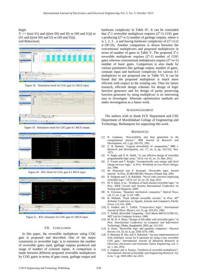
begin
Y <= ((not S1) and (((not S0) and I0) or (S0 and I1))) or
(S1 and (((not S0) and I2) or (S0 and I3)));
end Behavioral; ---------------------------------------------------------------------------------------
Figure 18. Simulation result for COG gate 4:1 MUX input.
Figure 19. Simulation result for COG gate 4:1 MUX output.
Figure 20. RTL block for COG gate 4:1 MUX input.
Figure 21. RTL schematic for COG gate 4:1 MUX input.
VII. CONCLUSION
In this paper, the reversible multiplexer using COG
gate is proposed and described. One of the major
constraints in reversible logic is to minimize the number
of reversible gates used, garbage outputs produced and
usage of number of constant inputs. A comparison is
made between different proposed reversible multiplexers
by COG gates in terms of gate count, garbage output and
hardware complexity in Table IV. It can be concluded
that 2n:1 reversible multiplexer requires (2
n-1) COG gate
s producing (2n+n-1) number of garbage outputs, where n
is 1, 2, 3…n and having hardware complexity of (2n-1) (2
α+2ß+2δ). Another comparison is drawn between the
conventional multiplexers and proposed multiplexers in
terms of number of gates in Table V. The proposed 2n:1
reversible multiplexer requires (2n-1) number of COG
gates whereas conventional multiplexers require (2n+n+1)
number of basic gates. Comparison is also made by
various parameters like garbage output, number of gates,
constant input and hardware complexity for various 4:1
multiplexer to our proposed one in Table VI. It can be
found that the proposed multiplexer is much more
efficient with respect to the existing one. Thus for future
research, efficient design schemes for design of logic
function generator and for design of parity preserving
function generator by using multiplexer is an interesting
area to investigate. Alternate optimization methods are
under investigation as a future work.
ACKNOWLEDGMENT
The authors wish to thank ECE Department and CSE
Department of Murshidabad College of Engineering and
Technology, Berhampore for supporting this work.
REFERENCES
[1] R. Landauer, “Irreversibility and heat generation in the
computational process,” IBM Journal of Research and Development, vol. 5, pp. 183-191, 1961.
[2] C. H. Bennett, “Logical reversibility of computation,” IBM J.
Research and Development, vol. 17, no. 6, pp. 525-532, Nov. 1973.
[3] P. Singla and N. K. Malik, “A cost effective design of reversible programmable logic array,” IJCA, vol. 41, no. 15, Mar. 2012.
[4] S. Younis and T. Knight, “Asymptotically zero energy split level
charge recovery logic,” in Proc. Workshop on Low Power Design, Jun. 1994.
[5] M. Perkowski and P. Kerntopf, “Reversible logic. Invited tutorial,” in Proc. EURO-MICRO, Warsaw, Poland, Sep. 2001.
[6] R. Saligram and T. R. Rakshith, “Novel code converter employing
reversible logic,” IJCA, vol. 52, no. 18, Aug. 2012.
[15] S. Gugnani and A. Kumar, “Synthesis of reversible multiplexers”,
International Journal of Scientific and Engineering Research, vol.
4, no. 7, pp. 1859-1863, Jul. 2013.
International Journal of Electronics and Electrical Engineering Vol. 3, No. 5, October 2015
©2015 Engineering and Technology Publishing 370
[7] M. S. Islam, et al., “Synthesis of fault tolerant reversible logic,” in
Proc. IEEE Circuits and Systems International Conference on Testing and Diagnosis, 2009.
[8] R. Feynman, “Quantum mechanical computers,” Optical News,
vol. 11, no. 2, pp. 11-20, 1985.[9] B. Parhami, “Fault tolerant reversible circuits,” in Proc. 40th
Asilomar Conference on Signals, Systems and Computers, Pacific Grove, CA, Oct. 2006.
[10] E. Fredkin and T. Toffoli, “Conservative logic,” International
Journal of Theor. Physics, vol. 21, pp. 219-253, 1982.[11] T. Toffoli, Reversible Computing - Tech Memo MIT/LCS/TM-151,
MIT Lab for Computer Science, 1980.[12] M. M. H. A. Khan, “Design of full-adder with reversible gates,” in
Proc. International Conference on Computer and Information
Technology, Dhaka, Bangladesh, 2002, pp. 515-519.[13] A. Peres, “Reversible logic and quantum computers,” Physical
Review, vol. 32, no. 6, pp. 3266-3276, 1985.[14] S. Mamataj, B. Das, and A. Rahaman, “An ease implementation of
4-bit arithmetic circuit for 8 operation by using a new reversible
COG gate,” International Journal of Advanced Research inElectrical, Electronics and Instrumen Tation Engineering, vol. 3,
no. 1, Jan. 2014.

[16] Praveen. B and Vinay Kumar S. B, “2n:1 reversible multiplexer and its transistor implementation,” International Journal of
Computational Engineering Research, vol. 2, no. 1, pp. 182-189,
2012. [17] R. Saligram, S. S. Hegde, S. A. Kulkarni, H. R. Bhagyalakshmi,
and M. K. Venkatesha, “Design of fault tolerant reversible multiplexer based multi-boolean function generator using parity
preserving gates,” International Journal of Computer Applications,
vol. 66, no. 19, pp. 20-24, Mar. 2013.
Mrs. Shefali Mamataj received B.Tech in Electronics and Communication Engineering
from University of Kalyani, West Bengal,
India in 2003 and also received M.Tech in Optics and Optoelectronics from University of
Calcutta, Kolkata, India in 2006. Her teaching experience is approximately nine years and
presently she is working as an Assistant
Professor, Department of Electronics and Communication Engineering, MCET,
Berhampore. Her present research of interests includes Reversible Logic, DNA Computing. She has authored 10 international journal papers, 2
international conference paper papers, one national conference paper
and another two accepted international conference papers in the areas of the Reversible Logic.
International Journal of Electronics and Electrical Engineering Vol. 3, No. 5, October 2015
©2015 Engineering and Technology Publishing 371
Mr. Biswajit Das was born in West Bengal,
India in 1977. He received Bachelor’s degree
in Computer Science Technology from University of Kalyani, West Bengal, India in
2002 and M.Tech degree in Computer Science & Engineering from University of Kalyani,
West Bengal, India in 2008. He is currently
works at MCET, Berhampore, West Bengal, India as Assistant Professor in CSE department.
His research of interest in Reversible Logic, Image Processing. He has co-authored 9
international journal papers, 2 international conference paper papers,
one national conference paper and another two accepted international conference papers in the area of the Reversible Logic.