Real-Time Clock (RTC) (Rev. B) - Texas · PDF file · 2016-09-12RθJB...
29
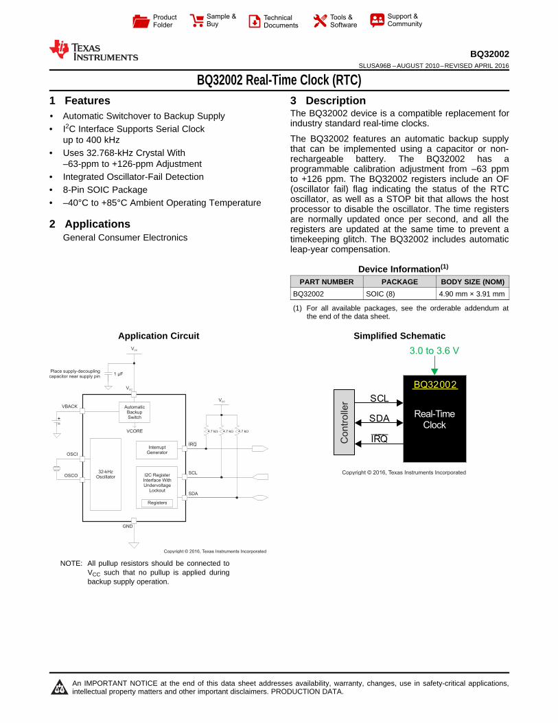
4.7 kW 4.7 kW 4.7 kW VBACK OSCI OSCO IRQ SCL SDA GND I2C Register Interface With Undervoltage Lockout 32-kHz Oscillator Automatic Backup Switch VCORE Interrupt Generator V CC V CC Registers Place supply-decoupling capacitor near supply pin 1 μF V CC Copyright © 2016, Texas Instruments Incorporated BQ32002 SCL SDA ____ IRQ 3.0 to 3.6 V Real-Time Clock Controller Copyright © 2016, Texas Instruments Incorporated Product Folder Sample & Buy Technical Documents Tools & Software Support & Community An IMPORTANT NOTICE at the end of this data sheet addresses availability, warranty, changes, use in safety-critical applications, intellectual property matters and other important disclaimers. PRODUCTION DATA. BQ32002 SLUSA96B – AUGUST 2010 – REVISED APRIL 2016 BQ32002 Real-Time Clock (RTC) 1 1 Features 1• Automatic Switchover to Backup Supply • I 2 C Interface Supports Serial Clock up to 400 kHz • Uses 32.768-kHz Crystal With –63-ppm to +126-ppm Adjustment • Integrated Oscillator-Fail Detection • 8-Pin SOIC Package • –40°C to +85°C Ambient Operating Temperature 2 Applications General Consumer Electronics 3 Description The BQ32002 device is a compatible replacement for industry standard real-time clocks. The BQ32002 features an automatic backup supply that can be implemented using a capacitor or non- rechargeable battery. The BQ32002 has a programmable calibration adjustment from –63 ppm to +126 ppm. The BQ32002 registers include an OF (oscillator fail) flag indicating the status of the RTC oscillator, as well as a STOP bit that allows the host processor to disable the oscillator. The time registers are normally updated once per second, and all the registers are updated at the same time to prevent a timekeeping glitch. The BQ32002 includes automatic leap-year compensation. Device Information (1) PART NUMBER PACKAGE BODY SIZE (NOM) BQ32002 SOIC (8) 4.90 mm × 3.91 mm (1) For all available packages, see the orderable addendum at the end of the data sheet. Application Circuit NOTE: All pullup resistors should be connected to V CC such that no pullup is applied during backup supply operation. Simplified Schematic
-
Upload
truongkiet -
Category
Documents
-
view
216 -
download
1
Transcript of Real-Time Clock (RTC) (Rev. B) - Texas · PDF file · 2016-09-12RθJB...
4.7 kW 4.7 kW 4.7 kW
VBACK
OSCI
OSCO
IRQ
SCL
SDA
GND
I2C RegisterInterface WithUndervoltage
Lockout
32-kHzOscillator
AutomaticBackupSwitch
VCORE
InterruptGenerator
VCC
VCC
Registers
Place supply-decouplingcapacitor near supply pin
1 µF
VCC
Copyright © 2016, Texas Instruments Incorporated
BQ32002
SCL
SDA____IRQ
3.0 to 3.6 V
Real-TimeClock
Contr
olle
r
Copyright © 2016, Texas Instruments Incorporated
Product
Folder
Sample &Buy
Technical
Documents
Tools &
Software
Support &Community
An IMPORTANT NOTICE at the end of this data sheet addresses availability, warranty, changes, use in safety-critical applications,intellectual property matters and other important disclaimers. PRODUCTION DATA.
BQ32002SLUSA96B –AUGUST 2010–REVISED APRIL 2016
BQ32002 Real-Time Clock (RTC)
1
1 Features1• Automatic Switchover to Backup Supply• I2C Interface Supports Serial Clock
up to 400 kHz• Uses 32.768-kHz Crystal With
–63-ppm to +126-ppm Adjustment• Integrated Oscillator-Fail Detection• 8-Pin SOIC Package• –40°C to +85°C Ambient Operating Temperature
2 ApplicationsGeneral Consumer Electronics
3 DescriptionThe BQ32002 device is a compatible replacement forindustry standard real-time clocks.
The BQ32002 features an automatic backup supplythat can be implemented using a capacitor or non-rechargeable battery. The BQ32002 has aprogrammable calibration adjustment from –63 ppmto +126 ppm. The BQ32002 registers include an OF(oscillator fail) flag indicating the status of the RTCoscillator, as well as a STOP bit that allows the hostprocessor to disable the oscillator. The time registersare normally updated once per second, and all theregisters are updated at the same time to prevent atimekeeping glitch. The BQ32002 includes automaticleap-year compensation.
Device Information(1)
PART NUMBER PACKAGE BODY SIZE (NOM)BQ32002 SOIC (8) 4.90 mm × 3.91 mm
(1) For all available packages, see the orderable addendum atthe end of the data sheet.
Application Circuit
NOTE: All pullup resistors should be connected toVCC such that no pullup is applied duringbackup supply operation.
Simplified Schematic
2
BQ32002SLUSA96B –AUGUST 2010–REVISED APRIL 2016 www.ti.com
Product Folder Links: BQ32002
Submit Documentation Feedback Copyright © 2010–2016, Texas Instruments Incorporated
Table of Contents1 Features .................................................................. 12 Applications ........................................................... 13 Description ............................................................. 14 Revision History..................................................... 25 Pin Configuration and Functions ......................... 36 Specifications......................................................... 4
6.1 Absolute Maximum Ratings ..................................... 46.2 ESD Ratings.............................................................. 46.3 Recommended Operating Conditions....................... 46.4 Thermal Information .................................................. 46.5 Electrical Characteristics........................................... 56.6 Timing Requirements ................................................ 66.7 Typical Characteristics .............................................. 6
7 Detailed Description .............................................. 77.1 Overview ................................................................... 77.2 Functional Block Diagram ......................................... 77.3 Feature Description................................................... 7
7.4 Device Functional Modes........................................ 107.5 Programming........................................................... 107.6 Register Maps ......................................................... 12
8 Application and Implementation ........................ 198.1 Application Information............................................ 198.2 Typical Application .................................................. 19
9 Power Supply Recommendations ...................... 2110 Layout................................................................... 21
10.1 Layout Guidelines ................................................. 2110.2 Layout Example .................................................... 21
11 Device and Documentation Support ................. 2211.1 Community Resources.......................................... 2211.2 Trademarks ........................................................... 2211.3 Electrostatic Discharge Caution............................ 2211.4 Glossary ................................................................ 22
12 Mechanical, Packaging, and OrderableInformation ........................................................... 22
4 Revision History
Changes from Revision A (December 2010) to Revision B Page
• Added Pin Configuration and Functions section, ESD Ratings section, Thermal Information section, DetailedDescription section, Device and Documentation Support section, and Mechanical, Packaging, and OrderableInformation section ................................................................................................................................................................ 1
• Deleted Trickle Charge Pump from Functional Block Diagram/Application Circuit ............................................................... 1• Changed Crystal series resistance maximum from 40 kΩ to 70 kΩ in Recommended Operating Conditions ...................... 4• Added Recommended Operating Conditions table note (1) Crystal load capacitance ±10% is allowed. ............................. 4
1
2
3
4 5
6
7
8
SDA
SCL
IRQ
VCC
GND
VBACK
OSCO
OSCI
3
BQ32002www.ti.com SLUSA96B –AUGUST 2010–REVISED APRIL 2016
Product Folder Links: BQ32002
Submit Documentation FeedbackCopyright © 2010–2016, Texas Instruments Incorporated
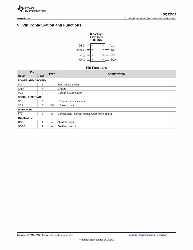
5 Pin Configuration and Functions
D Package8-Pin SOICTop View
Pin FunctionsPIN
TYPE DESCRIPTIONNAME NO.POWER AND GROUNDVCC 8 — Main device powerGND 4 — GroundVBACK 3 — Backup device powerSERIAL INTERFACESCL 6 I I2C serial interface clockSDA 5 I/O I2C serial dataINTERRUPTIRQ 7 O Configurable interrupt output. Open-drain output.OSCILLATOROSCI 1 — Oscillator inputOSCO 2 — Oscillator output

4
BQ32002SLUSA96B –AUGUST 2010–REVISED APRIL 2016 www.ti.com
Product Folder Links: BQ32002
Submit Documentation Feedback Copyright © 2010–2016, Texas Instruments Incorporated
(1) Stresses beyond those listed under Absolute Maximum Ratings may cause permanent damage to the device. These are stress ratingsonly, which do not imply functional operation of the device at these or any other conditions beyond those indicated under RecommendedOperating Conditions. Exposure to absolute-maximum-rated conditions for extended periods may affect device reliability.
6 Specifications
6.1 Absolute Maximum Ratings (1)
over operating free-air temperature range (unless otherwise noted)MIN MAX UNIT
VIN Input voltageVCC to GND –0.3 4
VAll other pins to GND –0.3 VCC + 0.3
TJ Operating junction temperature –40 150 °CTstg Storage temperature after reflow –60 150 °C
(1) JEDEC document JEP155 states that 500-V HBM allows safe manufacturing with a standard ESD control process.(2) JEDEC document JEP157 states that 250-V CDM allows safe manufacturing with a standard ESD control process.
6.2 ESD RatingsVALUE UNIT
V(ESD) Electrostatic dischargeHuman-body model (HBM), per ANSI/ESDA/JEDEC JS-001 (1) 2000
VCharged-device model (CDM), per JEDEC specification JESD22-C101 (2) 500
(1) Crystal load capacitance ±10% is allowed.
6.3 Recommended Operating ConditionsMIN NOM MAX UNIT
VCC Supply voltage, VCC to GND 3 3.6 VTA Operating free-air temperature –40 85 °Cfo Crystal resonant frequency 32.768 kHzRS Crystal series resistance 70 kΩCL Crystal load capacitance (1) 12 pF
(1) For more information about traditional and new thermal metrics, see the Semiconductor and IC Package Thermal Metrics applicationreport, SPRA953.
6.4 Thermal Information
THERMAL METRIC (1)BQ32002
UNITD (SOIC)8 PINS
RθJA Junction-to-ambient thermal resistance 114.8 °C/WRθJC(top) Junction-to-case (top) thermal resistance 59.1 °C/WRθJB Junction-to-board thermal resistance 55.5 °C/WψJT Junction-to-top characterization parameter 11.9 °C/WψJB Junction-to-board characterization parameter 55 °C/W

5
BQ32002www.ti.com SLUSA96B –AUGUST 2010–REVISED APRIL 2016
Product Folder Links: BQ32002
Submit Documentation FeedbackCopyright © 2010–2016, Texas Instruments Incorporated
(1) The backup supply current is measured only after an initial power up. The device behavior is not ensured before the first power up.(2) Typical accuracy is measured using reference board design and KDS DMX-26S surface-mount 32.768-kHz crystal. Variation in board
design and crystal section results in different typical accuracy.
6.5 Electrical Characteristicsover operating free-air temperature range (unless otherwise noted)
PARAMETER TEST CONDITION MIN TYP MAX UNITPOWER SUPPLYICC VCC supply current 65 200 μA
VBACK Backup supply voltageOperating 1.4 VCC VSwitchover 2 VCC
IBACK Backup supply current VCC = 0 V, VBAT = 3 V, Oscillator on, TA = 25°C 0.9 (1) 1.5 μA
VSO Switchover voltageOperating → Backup 1.8
VBackup → Operating 2.4
LOGIC LEVEL INPUTSVIL Input low voltage 0.3 × VCC VVIH Input high voltage 0.7 × VCC VIIN Input current 0 V ≤ VIN ≤ VCC –1 1 μALOGIC LEVEL OUTPUTSVOL Output low voltage IOL = 3 mA 0.4 VIL Leakage current –1 1 μAREAL-TIME CLOCK CHARACTERISTICS
Pre-calibration accuracy VCC = 3.3 V, VBAT = 3 V, Oscillator on, TA = 25°C ±35 (2) ppm
-10
0
10
20
30
40
50
60
70
80
90
100
20
25
30
35
40
45
50
0.5 1.0 1.5 2.0 2.5 3.0
I bac
k (u
A)
I CC (
uA)
Vbackup (V)
Icc (uA)
Iback (uA)
C001
VCC = 2 V
-10
-5
0
5
10
15
20
100
101.5
103
104.5
106
107.5
2.4 2.9 3.4 3.9
I bac
k (u
A)
I CC (
uA)
Vbackup (V)
Icc (uA)
Iback (uA)
C002
VCC = 3.3 V
6
BQ32002SLUSA96B –AUGUST 2010–REVISED APRIL 2016 www.ti.com
Product Folder Links: BQ32002
Submit Documentation Feedback Copyright © 2010–2016, Texas Instruments Incorporated
(1) Cb = total capacitance of one bus line in pF
6.6 Timing Requirements
PARAMETERSTANDARD MODE FAST MODE
UNITMIN NOM MAX MIN NOM MAX
fscl I2C clock frequency 0 100 0 400 kHztsch I2C clock high time 4 0.6 μstscl I2C clock low time 4.7 1.3 μstsp I2C spike time 0 50 0 50 nstsds I2C serial data setup time 250 100 nstsdh I2C serial data hold time 0 0 nsticr I2C input rise time 1000 20 + 0.1Cb
(1) 300 nsticf I2C input fall time 300 20 + 0.1Cb
(1) 300 nstocf I2C output fall time 300 20 + 0.1Cb
(1) 300 μstbuf I2C bus free time 4.7 1.3 μststs I2C Start setup time 4.7 0.6 μststh I2C Start hold time 4 0.6 μstsps I2C Stop setup time 4 0.6 μstvd (data) Valid data time (SCL low to SDA valid) 1 1 μs
tvd (ack)Valid data time of ACK(ACK signal from SCL low to SDA low) 1 1 μs
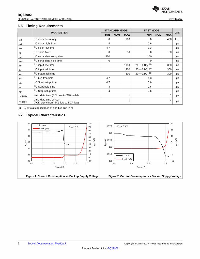
6.7 Typical Characteristics
Figure 1. Current Consumption vs Backup Supply Voltage Figure 2. Current Consumption vs Backup Supply Voltage
I2C Register Interface With Undervoltage
Lockout
Interrupt Generator
32-kHz Oscillator
VCORE
Registers
Automatic Backup Switch VCC
4.7 N 4.7 N 4.7 N
VCC
VCC
IRQ
SCL
SDA
GND
OSCO
OSCI
VBACK
1 µF
.22 F
Place supply-decoupling capacitor near supply pin
Use only super-capacitor
or battery, not both
Copyright © 2016, Texas Instruments Incorporated
7
BQ32002www.ti.com SLUSA96B –AUGUST 2010–REVISED APRIL 2016
Product Folder Links: BQ32002
Submit Documentation FeedbackCopyright © 2010–2016, Texas Instruments Incorporated
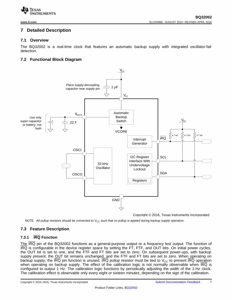
7 Detailed Description
7.1 OverviewThe BQ32002 is a real-time clock that features an automatic backup supply with integrated oscillator-faildetection.
7.2 Functional Block Diagram
NOTE: All pullup resistors should be connected to VCC such that no pullup is applied during backup supply operation.
7.3 Feature Description
7.3.1 IRQ FunctionThe IRQ pin of the BQ32002 functions as a general-purpose output or a frequency test output. The function ofIRQ is configurable in the device register space by setting the FT, FTF, and OUT bits. On initial power cycles,the OUT bit is set to one, and the FTF and FT bits are set to zero. On subsequent power-ups, with backupsupply present, the OUT bit remains unchanged, and the FTF and FT bits are set to zero. When operating onbackup supply, the IRQ pin function is unused. IRQ pullup resistor must be tied to VCC to prevent IRQ operationwhen operating on backup supply. The effect of the calibration logic is not normally observable when IRQ isconfigured to output 1 Hz. The calibration logic functions by periodically adjusting the width of the 1-Hz clock.The calibration effect is observable only every eight or sixteen minutes, depending on the sign of the calibration.

8
BQ32002SLUSA96B –AUGUST 2010–REVISED APRIL 2016 www.ti.com
Product Folder Links: BQ32002
Submit Documentation Feedback Copyright © 2010–2016, Texas Instruments Incorporated
Feature Description (continued)
Figure 3. IRQ Pin Functional Diagram
Table 1. IRQ FunctionFT OUT FTF IRQ STATE1 X 1 1 Hz1 X 0 512 Hz0 1 X 10 0 X 0

3.3V
VBACK
VRE F
V CC
–5 V/ms (max)
3.3V
VBACK
VRE F
On VBACK On VBACK On VCCOn VCC
VBACK > VREF VBACK > VREF
3.3V
VRE F
VBACK
On VBACKOn VCC
VREF > VBACK
3.3V
VRE F
VBACK
On VBACK On VCC
VREF > VBACK
Vo
ltage
Vo
ltage
Vo
ltage
Vo
ltage
T ime
T ime Time
Time
V CC
V CCV CC
–5 V/ms (max)
9
BQ32002www.ti.com SLUSA96B –AUGUST 2010–REVISED APRIL 2016
Product Folder Links: BQ32002
Submit Documentation FeedbackCopyright © 2010–2016, Texas Instruments Incorporated
7.3.2 VBACK SwitchoverThe BQ32002 has an internal switchover circuit that causes the device to switch from main power supply tobackup power supply when the voltage of the main supply pin VCC drops below a minimum threshold. The VBACKswitchover circuit uses an internal reference voltage VREF derived from the on-chip bandgap reference; VREF isapproximately 1.8 V. The device switches to the VBACK supply when VCC is less than the lesser of VBACK or VREF.Similarly, the device switches to the VCC supply when VCC is greater than either VBACK or VREF.
Some registers are reset to default values when the RTC switches from main power supply to backup powersupply. See the register definitions to determine what register bits are effected by a backup switchover (effectedbits have their reset value (1/0) shown for Cycle, bits that are unchanged by backup are marked UC).
The time-keeping registers can take up to 1 second to update after the RTC switches from backup power supplyto main power supply.
Figure 4. Switchover Diagram

10
BQ32002SLUSA96B –AUGUST 2010–REVISED APRIL 2016 www.ti.com
Product Folder Links: BQ32002
Submit Documentation Feedback Copyright © 2010–2016, Texas Instruments Incorporated
7.4 Device Functional ModesWhen the device switches from the main power supply to backup supply, the time-keeping registers [0- 9] cannotbe accessed through the I2C. The access to these registers are only when VCC > VREF. The time-keepingregisters can take up to 1 second to update after the device switches from backup power supply to main powersupply.
7.5 Programming
7.5.1 I2C Serial InterfaceThe I2C interface allows control and monitoring of the RTC by a microcontroller. I2C is a two-wire serial interfacedeveloped by Philips Semiconductor (see I2C-Bus Specification, Version 2.1, January 2000).
The bus consists of a data line (SDA) and a clock line (SCL) with off-chip pullup resistors. When the bus is idle,both SDA and SCL lines are pulled high.
A master device, usually a microcontroller or a digital signal processor, controls the bus. The master isresponsible for generating the SCL signal and device addresses. The master also generates specific conditionsthat indicate the START and STOP of data transfer.
A slave device receives and/or transmits data on the bus under control of the master device. This deviceoperates only as a slave device.
I2C communication is initiated by a master sending a start condition, a high-to-low transition on the SDA I/O whileSCL is held high. After the start condition, the device address byte is sent, most-significant bit (MSB) first,including the data direction bit (R/W). After receiving a valid address byte, this device responds with anacknowledge, a low on the SDA I/O during the high of the acknowledge-related clock pulse. This deviceresponds to the I2C slave address 11010000b for write commands and slave address 11010001b for readcommands.
This device does not respond to the general call address.
A data byte follows the address acknowledge. If the R/W bit is low, the data is written from the master. If the R/Wbit is high, the data from this device are the values read from the register previously selected by a write to thesubaddress register. The data byte is followed by an acknowledge sent from this device. Data is output only ifcomplete bytes are received and acknowledged.
A stop condition, which is a low-to-high transition on the SDA I/O while the SCL input is high, is sent by themaster to terminate the transfer. A master device must wait at least 60 μs after the RTC exits backup mode togenerate a START condition.

S1 1 1
0 0 0 0 W
Slave
Address AC
K
(A )N
AC
KSub
Address
STA
RT
S
STA
RT
1 1 1
0 0 0 0
R
Slave
Address AC
K
(D )N
AC
KDataN
(D )N+1
NA
CKDataN+1
ST
OP
0.7 VCC
0.3 VCC
0.7 VCC
0.3 VCC
0.7 VCC
0.3 VCC
0.7 VCC
0.3 VCC
SDA
SCL
Start Condition
SDA
SCL
Start Condition
Stop Condition
8 9
tsps
ticf ticr tsdh tvd
tvd tbuf
D7/A
ticf ticr tsds
tsds
tsth
tsch
tscl
1/fscl
1 2 3 4
11
BQ32002www.ti.com SLUSA96B –AUGUST 2010–REVISED APRIL 2016
Product Folder Links: BQ32002
Submit Documentation FeedbackCopyright © 2010–2016, Texas Instruments Incorporated
Programming (continued)
Figure 5. I2C Timing Diagram
Figure 6. I2C Read Mode
Figure 7. I2C Write Mode

12
BQ32002SLUSA96B –AUGUST 2010–REVISED APRIL 2016 www.ti.com
Product Folder Links: BQ32002
Submit Documentation Feedback Copyright © 2010–2016, Texas Instruments Incorporated
7.6 Register Maps
Table 2. Normal Registers
REGISTER ADDRESS(HEX) REGISTER NAME DESCRIPTION
0 0x00 SECONDS Clock seconds and STOP bit1 0x01 MINUTES Clock minutes2 0x02 CENT_HOURS Clock hours, century, and CENT_EN bit3 0x03 DAY Clock day4 0x04 DATE Clock date5 0x05 MONTH Clock month6 0x06 YEARS Clock years7 0x07 CAL_CFG1 Calibration and configuration9 0x09 CFG2 Configuration 2
Table 3. Special Function Registers
REGISTER ADDRESS(HEX) REGISTER NAME DESCRIPTION
32 0x20 SF KEY 1 Special function key 133 0x21 SF KEY 2 Special function key 234 0x22 SFR Special function register
7.6.1 I2C Read After Backup ModeThe time-keeping registers can take up to 1 second to update after the RTC switches from backup power supplyto main power supply. An I2C read of the RTC that starts before the update has completed will return the timewhen the RTC enters backup mode. To ensure that the correct time is read after backup mode, the host shouldwait longer than 1 second after the main supply is greater than 2.8 V and VBACK.

13
BQ32002www.ti.com SLUSA96B –AUGUST 2010–REVISED APRIL 2016
Product Folder Links: BQ32002
Submit Documentation FeedbackCopyright © 2010–2016, Texas Instruments Incorporated
7.6.2 Normal Register Descriptions
Table 4. SECONDS RegisterAddress 0x00Name SECONDSInitial Value 0XXXXXXbDescription Clock seconds and STOP bit
D7 D6 D5 D4 D3 D2 D1 D0 BIT(S)STOP 10_SECOND 1_SECOND Name
r/w r/w r/w Read/Write0 X X X X X X X Initial
UC UC UC UC UC UC UC UC Cycle
STOP Oscillator stop. The STOP bit is used to force the oscillator to stop oscillating. STOP is set to 0 on initial application ofpower, on all subsequent power cycles STOP remains unchanged. On initial power application STOP can be written to 1and then written to 0 to force start the oscillator.0 Normal1 Stop
10_SECOND BCD of tens of seconds. The 10_SECOND bits are the BCD representation of the number of tens of seconds on theclock. Valid values are 0 to 5. If invalid data is written to 10_SECOND, the clock will update with invalid data in10_SECOND until the counter rolls over; thereafter, the data in 10_SECOND is valid. Time keeping registers can take upto 1 second to update after the RTC switches from backup power supply to main power supply.
1_SECOND BCD of seconds. The 1_SECOND bits are the BCD representation of the number of seconds on the clock. Valid valuesare 0 to 9. If invalid data is written to 1_SECOND, the clock will update with invalid data in 1_SECOND until the counterrolls over; thereafter, the data in 1_SECOND is valid. Time keeping registers can take up to 1 second to update after theRTC switches from backup power supply to main power supply.
Table 5. MINUTES RegisterAddress 0x01Name MINUTESInitial Value 1XXXXXXbDescription Clock minutes
D7 D6 D5 D4 D3 D2 D1 D0 BIT(S)OF 10_MINUTE 1_MINUTE Namer/w r/w r/w Read/Write1 X X X X X X X Initial0 UC UC UC UC UC UC UC Cycle
OF Oscillator fail flag. The OF bit is a latched flag indicating when the 32.768-kHz oscillator has dropped at least fourconsecutive pulses. The OF flag is always set on initial power-up, and it can be cleared through the serial interface.When OF is 0, no oscillator failure has been detected. When OF is 1, the oscillator fail detect circuit has detected at leastfour consecutive dropped pulses.0 No failure detected1 Failure detected
10_MINUTE BCD of tens of minutes. The 10_MINUTE bits are the BCD representation of the number of tens of minutes on the clock.Valid values are 0 to 5. If invalid data is written to 10_MINUTE, the clock will update with invalid data in 10_MINUTE untilthe counter rolls over; thereafter, the data in 10_MINUTE is valid. Time keeping registers can take up to 1 second toupdate after the RTC switches from backup power supply to main power supply.
1_MINUTE BCD of minutes. The 1_MINUTE bits are the BCD representation of the number of minutes on the clock. Valid values are0 to 9. If invalid data is written to 1_MINUTE, the clock will update with invalid data in 1_MINUTE until the counter rollsover; thereafter, the data in 1_MINUTE is valid. Time keeping registers can take up to 1 second to update after the RTCswitches from backup power supply to main power supply.

14
BQ32002SLUSA96B –AUGUST 2010–REVISED APRIL 2016 www.ti.com
Product Folder Links: BQ32002
Submit Documentation Feedback Copyright © 2010–2016, Texas Instruments Incorporated
Table 6. CENT_HOURS RegisterAddress 0x02Name CENT_HOURSInitial Value XXXXXXXXbDescription Clock hours, century, and CENT_EN bit
D7 D6 D5 D4 D3 D2 D1 D0 BIT(S)CENT_EN CENT 10_HOUR 1_HOUR Name
r/w r/w r/w r/w Read/WriteX X X X X X X X Initial
UC UC UC UC UC UC UC UC Cycle
CENT_EN Century enable. The CENT_EN bit enables the century timekeeping feature. If CENT_EN is set to 1, then the clocktracks the century using the CENT bit. If CENT_EN is set to 0, the clock ignores the CENT bit.0 Century disabled1 Century enabled
CENT Century. The CENT bit tracks the century when century timekeeping is enabled. The clock toggles the CENT bit whenthe year count rolls from 99 to 00. Because the clock compliments the CENT bit, the user can define the meaning ofCENT (1 for current century and 0 for next century, or 0 for current century and 1 for next century).
10_HOUR BCD of tens of hours (24-hour format). The 10_HOUR bits are the BCD representation of the number of tens of hours onthe clock, in 24-hour format. Valid values are 0 to 2. If invalid data is written to 10_HOUR, the clock will update withinvalid data in 10_HOUR until the counter rolls over; thereafter, the data in 10_HOUR is valid. Time keeping registers cantake up to 1 second to update after the RTC switches from backup power supply to main power supply.
1_HOUR BCD of hours (24-hour format). The 1_HOUR bits are the BCD representation of the number of hours on the clock, in 24-hour format. Valid values are 0 to 9. If invalid data is written to 1_HOUR, the clock will update with invalid data in1_HOUR until the counter rolls over; thereafter, the data in 1_HOUR is valid. Time keeping registers can take up to 1second to update after the RTC switches from backup power supply to main power supply.
Table 7. DAY RegisterAddress 0x03Name DAYInitial Value 00000XXXbDescription Clock day
D7 D6 D5 D4 D3 D2 D1 D0 BIT(S)RSVD DAY Name
r/w r/w Read/Write0 0 0 0 0 X X X Initial0 0 0 0 0 UC UC UC Cycle
RSVD Reserved. The RSVD bits should always be written as 0.DAY BCD of the day of the week. The DAY bits are the BCD representation of the day of the week. Valid values are 1 to 7
and represent the days from Sunday to Saturday. DAY updates if set to 0 until the counter rolls over; thereafter, the datain DAY is valid. Time keeping registers can take up to 1 second to update after the RTC switches from backup powersupply to main power supply.1 Sunday2 Monday3 Tuesday4 Wednesday5 Thursday6 Friday7 Saturday
15
BQ32002www.ti.com SLUSA96B –AUGUST 2010–REVISED APRIL 2016
Product Folder Links: BQ32002
Submit Documentation FeedbackCopyright © 2010–2016, Texas Instruments Incorporated
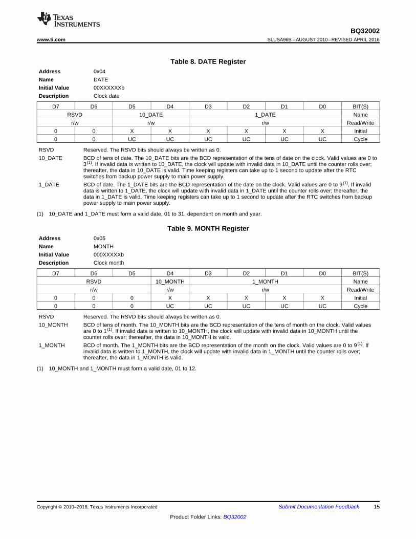
(1) 10_DATE and 1_DATE must form a valid date, 01 to 31, dependent on month and year.
Table 8. DATE RegisterAddress 0x04Name DATEInitial Value 00XXXXXXbDescription Clock date
D7 D6 D5 D4 D3 D2 D1 D0 BIT(S)RSVD 10_DATE 1_DATE Name
r/w r/w r/w Read/Write0 0 X X X X X X Initial0 0 UC UC UC UC UC UC Cycle
RSVD Reserved. The RSVD bits should always be written as 0.10_DATE BCD of tens of date. The 10_DATE bits are the BCD representation of the tens of date on the clock. Valid values are 0 to
3 (1). If invalid data is written to 10_DATE, the clock will update with invalid data in 10_DATE until the counter rolls over;thereafter, the data in 10_DATE is valid. Time keeping registers can take up to 1 second to update after the RTCswitches from backup power supply to main power supply.
1_DATE BCD of date. The 1_DATE bits are the BCD representation of the date on the clock. Valid values are 0 to 9 (1). If invaliddata is written to 1_DATE, the clock will update with invalid data in 1_DATE until the counter rolls over; thereafter, thedata in 1_DATE is valid. Time keeping registers can take up to 1 second to update after the RTC switches from backuppower supply to main power supply.
(1) 10_MONTH and 1_MONTH must form a valid date, 01 to 12.
Table 9. MONTH RegisterAddress 0x05Name MONTHInitial Value 000XXXXXbDescription Clock month
D7 D6 D5 D4 D3 D2 D1 D0 BIT(S)RSVD 10_MONTH 1_MONTH Name
r/w r/w r/w Read/Write0 0 0 X X X X X Initial0 0 0 UC UC UC UC UC Cycle
RSVD Reserved. The RSVD bits should always be written as 0.10_MONTH BCD of tens of month. The 10_MONTH bits are the BCD representation of the tens of month on the clock. Valid values
are 0 to 1 (1). If invalid data is written to 10_MONTH, the clock will update with invalid data in 10_MONTH until thecounter rolls over; thereafter, the data in 10_MONTH is valid.
1_MONTH BCD of month. The 1_MONTH bits are the BCD representation of the month on the clock. Valid values are 0 to 9 (1). Ifinvalid data is written to 1_MONTH, the clock will update with invalid data in 1_MONTH until the counter rolls over;thereafter, the data in 1_MONTH is valid.
16
BQ32002SLUSA96B –AUGUST 2010–REVISED APRIL 2016 www.ti.com
Product Folder Links: BQ32002
Submit Documentation Feedback Copyright © 2010–2016, Texas Instruments Incorporated
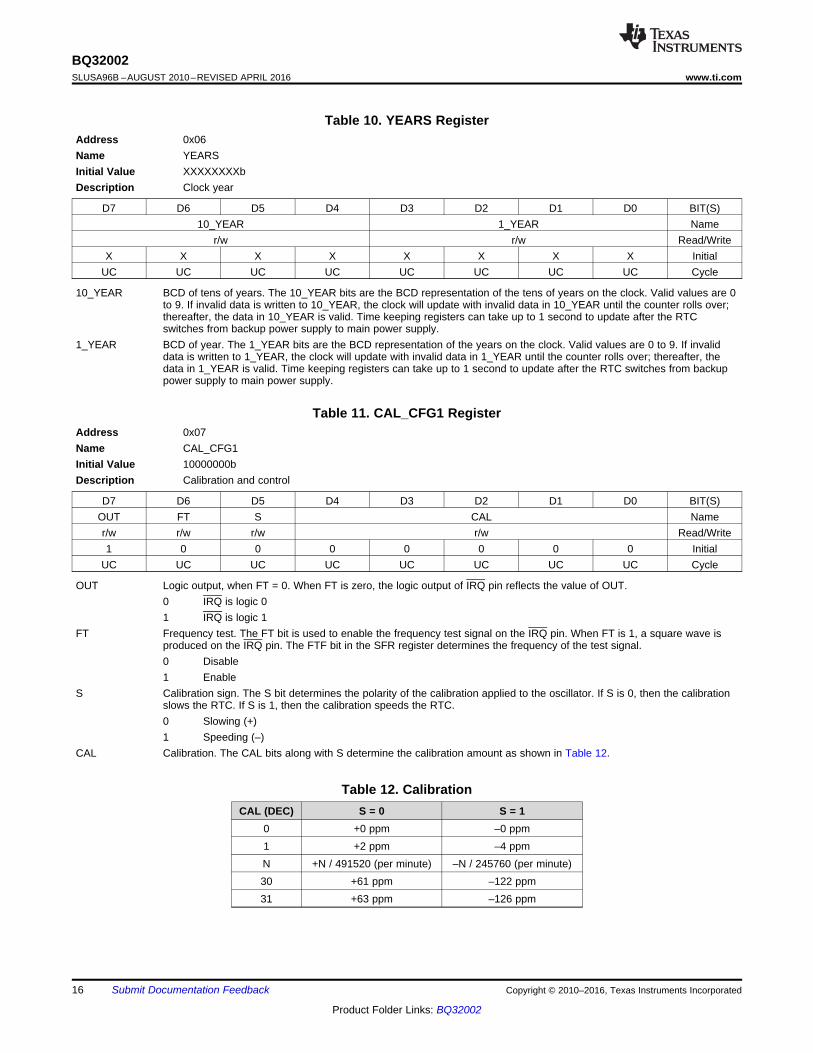
Table 10. YEARS RegisterAddress 0x06Name YEARSInitial Value XXXXXXXXbDescription Clock year
D7 D6 D5 D4 D3 D2 D1 D0 BIT(S)10_YEAR 1_YEAR Name
r/w r/w Read/WriteX X X X X X X X Initial
UC UC UC UC UC UC UC UC Cycle
10_YEAR BCD of tens of years. The 10_YEAR bits are the BCD representation of the tens of years on the clock. Valid values are 0to 9. If invalid data is written to 10_YEAR, the clock will update with invalid data in 10_YEAR until the counter rolls over;thereafter, the data in 10_YEAR is valid. Time keeping registers can take up to 1 second to update after the RTCswitches from backup power supply to main power supply.
1_YEAR BCD of year. The 1_YEAR bits are the BCD representation of the years on the clock. Valid values are 0 to 9. If invaliddata is written to 1_YEAR, the clock will update with invalid data in 1_YEAR until the counter rolls over; thereafter, thedata in 1_YEAR is valid. Time keeping registers can take up to 1 second to update after the RTC switches from backuppower supply to main power supply.
Table 11. CAL_CFG1 RegisterAddress 0x07Name CAL_CFG1Initial Value 10000000bDescription Calibration and control
D7 D6 D5 D4 D3 D2 D1 D0 BIT(S)OUT FT S CAL Namer/w r/w r/w r/w Read/Write1 0 0 0 0 0 0 0 Initial
UC UC UC UC UC UC UC UC Cycle
OUT Logic output, when FT = 0. When FT is zero, the logic output of IRQ pin reflects the value of OUT.0 IRQ is logic 01 IRQ is logic 1
FT Frequency test. The FT bit is used to enable the frequency test signal on the IRQ pin. When FT is 1, a square wave isproduced on the IRQ pin. The FTF bit in the SFR register determines the frequency of the test signal.0 Disable1 Enable
S Calibration sign. The S bit determines the polarity of the calibration applied to the oscillator. If S is 0, then the calibrationslows the RTC. If S is 1, then the calibration speeds the RTC.0 Slowing (+)1 Speeding (–)
CAL Calibration. The CAL bits along with S determine the calibration amount as shown in Table 12.
Table 12. CalibrationCAL (DEC) S = 0 S = 1
0 +0 ppm –0 ppm1 +2 ppm –4 ppmN +N / 491520 (per minute) –N / 245760 (per minute)30 +61 ppm –122 ppm31 +63 ppm –126 ppm
17
BQ32002www.ti.com SLUSA96B –AUGUST 2010–REVISED APRIL 2016
Product Folder Links: BQ32002
Submit Documentation FeedbackCopyright © 2010–2016, Texas Instruments Incorporated
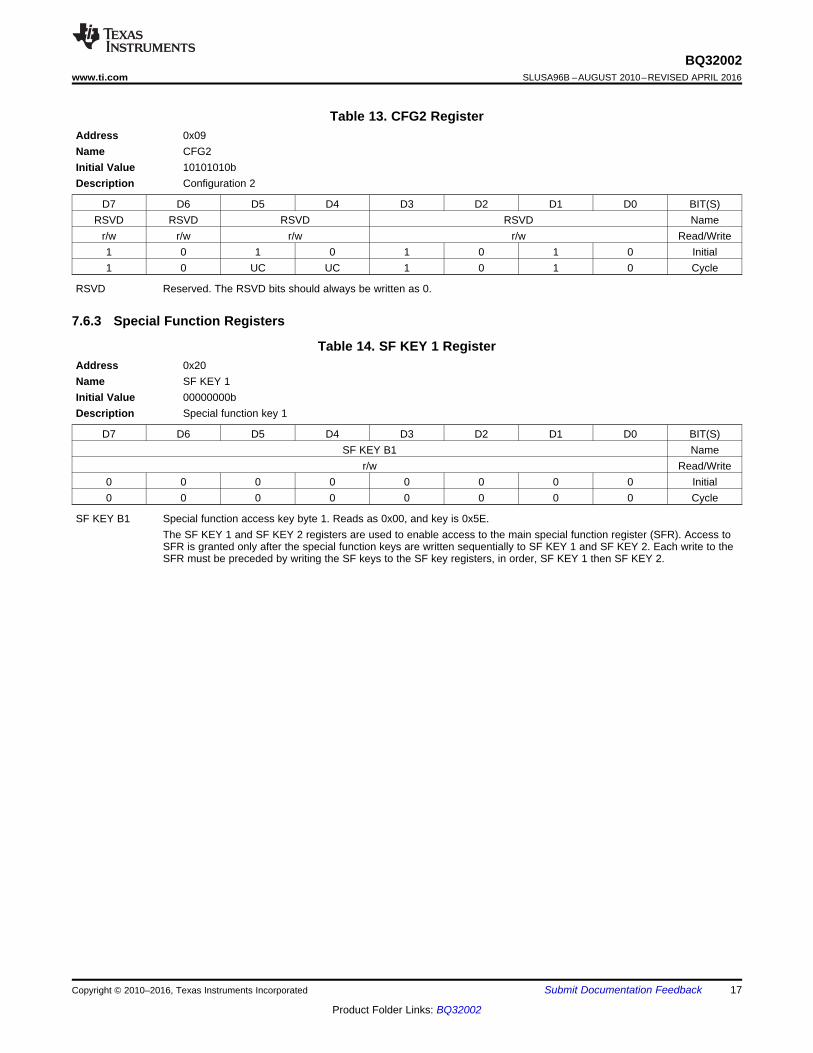
Table 13. CFG2 RegisterAddress 0x09Name CFG2Initial Value 10101010bDescription Configuration 2
D7 D6 D5 D4 D3 D2 D1 D0 BIT(S)RSVD RSVD RSVD RSVD Name
r/w r/w r/w r/w Read/Write1 0 1 0 1 0 1 0 Initial1 0 UC UC 1 0 1 0 Cycle
RSVD Reserved. The RSVD bits should always be written as 0.
7.6.3 Special Function Registers
Table 14. SF KEY 1 RegisterAddress 0x20Name SF KEY 1Initial Value 00000000bDescription Special function key 1
D7 D6 D5 D4 D3 D2 D1 D0 BIT(S)SF KEY B1 Name
r/w Read/Write0 0 0 0 0 0 0 0 Initial0 0 0 0 0 0 0 0 Cycle
SF KEY B1 Special function access key byte 1. Reads as 0x00, and key is 0x5E.The SF KEY 1 and SF KEY 2 registers are used to enable access to the main special function register (SFR). Access toSFR is granted only after the special function keys are written sequentially to SF KEY 1 and SF KEY 2. Each write to theSFR must be preceded by writing the SF keys to the SF key registers, in order, SF KEY 1 then SF KEY 2.

18
BQ32002SLUSA96B –AUGUST 2010–REVISED APRIL 2016 www.ti.com
Product Folder Links: BQ32002
Submit Documentation Feedback Copyright © 2010–2016, Texas Instruments Incorporated
Table 15. SF KEY 2 RegisterAddress 0x21Name SF KEY 2Initial Value 00000000bDescription Special function key 2
D7 D6 D5 D4 D3 D2 D1 D0 BIT(S)SF KEY 2 Name
r/w Read/Write0 0 0 0 0 0 0 0 Initial0 0 0 0 0 0 0 0 Cycle
SF KEY 2 Special function access key byte 2. Reads as 0x00, and key is 0xC7.The SF KEY 1 and SF KEY 2 registers are used to enable access to the main special function register (SFR). Access toSFR is granted only after the special function keys are written sequentially to SF KEY 1 and SF KEY 2. Each write to theSFR must be preceded by writing the SF keys to the SF key registers, in order, SF KEY 1 then SF KEY 2.
Table 16. SFR RegisterAddress 0x22Name SFRInitial Value 00000000bDescription Special function register 1
D7 D6 D5 D4 D3 D2 D1 D0 BIT(S)RSVD FTF Name
r/w r/w Read/Write0 0 0 0 0 0 0 0 Initial0 0 0 0 0 0 0 0 Cycle
RSVD Reserved. The RSVD bits should always be written as 0.FTF Force calibration to 1 Hz. FTF allows the frequency of the calibration output to be changed from 512 Hz to 1 Hz. By
default, FTF is cleared, and the RTC outputs a 512-Hz calibration signal. Setting FTF forces the calibration signal to 1Hz, and the calibration tracks the internal ppm adjustment. Note: The default 512-Hz calibration signal does not includethe effect of the ppm adjustment.0 Normal 512-Hz calibration1 1-Hz calibration

OSCI
OSCO
VBACK
GND
VCC
IRQ
SCL
SDA
VCC
bq32002
4.7 kΩ 4.7 kΩ
1 µF
4.7 kΩ
32.768 kHz
Copyright © 2016, Texas Instruments Incorporated
19
BQ32002www.ti.com SLUSA96B –AUGUST 2010–REVISED APRIL 2016
Product Folder Links: BQ32002
Submit Documentation FeedbackCopyright © 2010–2016, Texas Instruments Incorporated
8 Application and Implementation
NOTEInformation in the following applications sections is not part of the TI componentspecification, and TI does not warrant its accuracy or completeness. TI’s customers areresponsible for determining suitability of components for their purposes. Customers shouldvalidate and test their design implementation to confirm system functionality.
8.1 Application InformationThe typical application for the BQ32002 is to provide precise time and date to a system. The backup powersupply provides additional reliability by automatically switching over from the main supply when it drops under thevoltage threshold.
8.2 Typical ApplicationThe following design is a common application of the BQ32002.
Figure 8. Typical Application Schematic
8.2.1 Design RequirementsTable 17 lists the parameters for this design example.
Table 17. Design ParametersDESIGN PARAMETER REFERENCE EXAMPLE VALUE
Supply Voltage VCC 3.3 VBackup Supply VBACK BR1225
Crystal Oscillator XT 32.768 kHz

20
BQ32002SLUSA96B –AUGUST 2010–REVISED APRIL 2016 www.ti.com
Product Folder Links: BQ32002
Submit Documentation Feedback Copyright © 2010–2016, Texas Instruments Incorporated
8.2.2 Detailed Design Procedure
8.2.2.1 Reading From a RegisterThe report details the read-back of the SECONDS register. Figure 9 depicts the first condition that will be usedas a benchmark to compare the values taken from the SECONDS register in the BQ32002, to the internal PCtime of the oscilloscope. In this example two modes of operation are demonstrated.
Condition 1 The main power supply, VCC, is greater than the backup power supply, VBACK, and the internalreference voltage, VREF. In this mode, the device's internal registers are fully operational with READand WRITE access. Analyzing Figure 9, the known register values are compared to the systemclock; in this case, the PC clock which is shown at the bottom of the screen capture.
The BQ32002 during this condition is reading back [101][0010]= [5][2], which corresponds to52 seconds at PC time of 2:22:43 PM.
Condition 2 VCC is now lowered to 2 V (VBACK > VCC). In this mode, the I2C communications are halted.However, the internal time-keeping registers maintain full functional operation and accuracy whichwill be available to be reliably read by the controller 1 second after the RTC switches from VBACK toVCC supply.
Condition 3 During this final test condition, the RTC is restored to operate from the main power supply and I2Ccommunications are now fully functional.
Figure 10 demonstrates a read-back value from the SECONDS register of [100][0101]=[4][5], or 45 seconds at PC time of 2:23:36 PM. This proves that the BQ32002 managed toaccurately maintain the time-keeping registers functional while the VCC dropped below VBACK.
8.2.2.2 Leap Year CompensationThe BQ32002 classifies a leap year as any year that is evenly divisible by 4. Using this rule allows for reliableleap year compensation until 2100. Years that fall outside this rule will need to be compensated for by theexternal controller.
8.2.2.3 Utilizing the Backup SupplyIn order for the BQ32002 to achieve a low backup supply current as specified in the Electrical Characteristics,the VCC pin must be initialized after every total power loss situation. Initialization Is achieved by powering on VCCwith a voltage between 3 to 3.6 V for at least 1 ms immediately after the backup supply is connected. If the VCCis not powered on while connecting the backup supply, then the expected leakage current from VBACK will bemuch greater than specified.
8.2.3 Application Curves
Figure 9. Master and Slave I2C Communication for theSECONDS Register
Figure 10. Master and Slave I2C Communication for theSECONDS Register After Recovering from the Backup
Supply
OSCI
OSCO
VBACK
GND
VCC
SCL
SDA
____IRQ
1 µF
4.7
kΩ
0.22F
4.7
kΩ
4.7
kΩ
21
BQ32002www.ti.com SLUSA96B –AUGUST 2010–REVISED APRIL 2016
Product Folder Links: BQ32002
Submit Documentation FeedbackCopyright © 2010–2016, Texas Instruments Incorporated
9 Power Supply RecommendationsThe BQ32002 is designed to operate from an input voltage supply, VCC, range between 3 and 3.6 V. The usermust place a minimum of 1-µF ceramic bypass capacitor rated for at least the maximum voltage as close aspossible to VCC and GND pin.
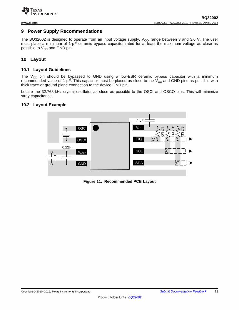
10 Layout
10.1 Layout GuidelinesThe VCC pin should be bypassed to GND using a low-ESR ceramic bypass capacitor with a minimumrecommended value of 1 µF. This capacitor must be placed as close to the VCC and GND pins as possible withthick trace or ground plane connection to the device GND pin.
Locate the 32.768-kHz crystal oscillator as close as possible to the OSCI and OSCO pins. This will minimizestray capacitance.
10.2 Layout Example
Figure 11. Recommended PCB Layout

22
BQ32002SLUSA96B –AUGUST 2010–REVISED APRIL 2016 www.ti.com
Product Folder Links: BQ32002
Submit Documentation Feedback Copyright © 2010–2016, Texas Instruments Incorporated
11 Device and Documentation Support
11.1 Community ResourcesThe following links connect to TI community resources. Linked contents are provided "AS IS" by the respectivecontributors. They do not constitute TI specifications and do not necessarily reflect TI's views; see TI's Terms ofUse.
TI E2E™ Online Community TI's Engineer-to-Engineer (E2E) Community. Created to foster collaborationamong engineers. At e2e.ti.com, you can ask questions, share knowledge, explore ideas and helpsolve problems with fellow engineers.
Design Support TI's Design Support Quickly find helpful E2E forums along with design support tools andcontact information for technical support.
11.2 TrademarksE2E is a trademark of Texas Instruments.All other trademarks are the property of their respective owners.
11.3 Electrostatic Discharge CautionThese devices have limited built-in ESD protection. The leads should be shorted together or the device placed in conductive foamduring storage or handling to prevent electrostatic damage to the MOS gates.
11.4 GlossarySLYZ022 — TI Glossary.
This glossary lists and explains terms, acronyms, and definitions.
12 Mechanical, Packaging, and Orderable InformationThe following pages include mechanical, packaging, and orderable information. This information is the mostcurrent data available for the designated devices. This data is subject to change without notice and revision ofthis document. For browser-based versions of this data sheet, refer to the left-hand navigation.
PACKAGE OPTION ADDENDUM
www.ti.com 21-Aug-2014
Addendum-Page 1
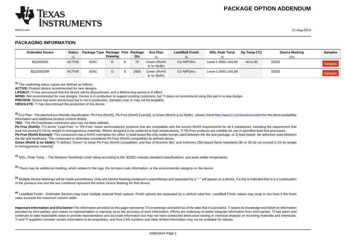
PACKAGING INFORMATION
Orderable Device Status(1)
Package Type PackageDrawing
Pins PackageQty
Eco Plan(2)
Lead/Ball Finish(6)
MSL Peak Temp(3)
Op Temp (°C) Device Marking(4/5)
Samples
BQ32002D ACTIVE SOIC D 8 75 Green (RoHS& no Sb/Br)
CU NIPDAU Level-1-260C-UNLIM -40 to 85 32002
BQ32002DR ACTIVE SOIC D 8 2500 Green (RoHS& no Sb/Br)
CU NIPDAU Level-1-260C-UNLIM 32002
(1) The marketing status values are defined as follows:ACTIVE: Product device recommended for new designs.LIFEBUY: TI has announced that the device will be discontinued, and a lifetime-buy period is in effect.NRND: Not recommended for new designs. Device is in production to support existing customers, but TI does not recommend using this part in a new design.PREVIEW: Device has been announced but is not in production. Samples may or may not be available.OBSOLETE: TI has discontinued the production of the device.
(2) Eco Plan - The planned eco-friendly classification: Pb-Free (RoHS), Pb-Free (RoHS Exempt), or Green (RoHS & no Sb/Br) - please check http://www.ti.com/productcontent for the latest availabilityinformation and additional product content details.TBD: The Pb-Free/Green conversion plan has not been defined.Pb-Free (RoHS): TI's terms "Lead-Free" or "Pb-Free" mean semiconductor products that are compatible with the current RoHS requirements for all 6 substances, including the requirement thatlead not exceed 0.1% by weight in homogeneous materials. Where designed to be soldered at high temperatures, TI Pb-Free products are suitable for use in specified lead-free processes.Pb-Free (RoHS Exempt): This component has a RoHS exemption for either 1) lead-based flip-chip solder bumps used between the die and package, or 2) lead-based die adhesive used betweenthe die and leadframe. The component is otherwise considered Pb-Free (RoHS compatible) as defined above.Green (RoHS & no Sb/Br): TI defines "Green" to mean Pb-Free (RoHS compatible), and free of Bromine (Br) and Antimony (Sb) based flame retardants (Br or Sb do not exceed 0.1% by weightin homogeneous material)
(3) MSL, Peak Temp. - The Moisture Sensitivity Level rating according to the JEDEC industry standard classifications, and peak solder temperature.
(4) There may be additional marking, which relates to the logo, the lot trace code information, or the environmental category on the device.
(5) Multiple Device Markings will be inside parentheses. Only one Device Marking contained in parentheses and separated by a "~" will appear on a device. If a line is indented then it is a continuationof the previous line and the two combined represent the entire Device Marking for that device.
(6) Lead/Ball Finish - Orderable Devices may have multiple material finish options. Finish options are separated by a vertical ruled line. Lead/Ball Finish values may wrap to two lines if the finishvalue exceeds the maximum column width.
Important Information and Disclaimer:The information provided on this page represents TI's knowledge and belief as of the date that it is provided. TI bases its knowledge and belief on informationprovided by third parties, and makes no representation or warranty as to the accuracy of such information. Efforts are underway to better integrate information from third parties. TI has taken andcontinues to take reasonable steps to provide representative and accurate information but may not have conducted destructive testing or chemical analysis on incoming materials and chemicals.TI and TI suppliers consider certain information to be proprietary, and thus CAS numbers and other limited information may not be available for release.
PACKAGE OPTION ADDENDUM
www.ti.com 21-Aug-2014
Addendum-Page 2
In no event shall TI's liability arising out of such information exceed the total purchase price of the TI part(s) at issue in this document sold by TI to Customer on an annual basis.

TAPE AND REEL INFORMATION
*All dimensions are nominal
Device PackageType
PackageDrawing
Pins SPQ ReelDiameter
(mm)
ReelWidth
W1 (mm)
A0(mm)
B0(mm)
K0(mm)
P1(mm)
W(mm)
Pin1Quadrant
BQ32002DR SOIC D 8 2500 330.0 12.4 6.4 5.2 2.1 8.0 12.0 Q1
PACKAGE MATERIALS INFORMATION
www.ti.com 21-Aug-2014
Pack Materials-Page 1
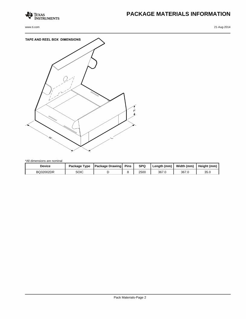
*All dimensions are nominal
Device Package Type Package Drawing Pins SPQ Length (mm) Width (mm) Height (mm)
BQ32002DR SOIC D 8 2500 367.0 367.0 35.0
PACKAGE MATERIALS INFORMATION
www.ti.com 21-Aug-2014
Pack Materials-Page 2


IMPORTANT NOTICE
Texas Instruments Incorporated and its subsidiaries (TI) reserve the right to make corrections, enhancements, improvements and otherchanges to its semiconductor products and services per JESD46, latest issue, and to discontinue any product or service per JESD48, latestissue. Buyers should obtain the latest relevant information before placing orders and should verify that such information is current andcomplete. All semiconductor products (also referred to herein as “components”) are sold subject to TI’s terms and conditions of salesupplied at the time of order acknowledgment.TI warrants performance of its components to the specifications applicable at the time of sale, in accordance with the warranty in TI’s termsand conditions of sale of semiconductor products. Testing and other quality control techniques are used to the extent TI deems necessaryto support this warranty. Except where mandated by applicable law, testing of all parameters of each component is not necessarilyperformed.TI assumes no liability for applications assistance or the design of Buyers’ products. Buyers are responsible for their products andapplications using TI components. To minimize the risks associated with Buyers’ products and applications, Buyers should provideadequate design and operating safeguards.TI does not warrant or represent that any license, either express or implied, is granted under any patent right, copyright, mask work right, orother intellectual property right relating to any combination, machine, or process in which TI components or services are used. Informationpublished by TI regarding third-party products or services does not constitute a license to use such products or services or a warranty orendorsement thereof. Use of such information may require a license from a third party under the patents or other intellectual property of thethird party, or a license from TI under the patents or other intellectual property of TI.Reproduction of significant portions of TI information in TI data books or data sheets is permissible only if reproduction is without alterationand is accompanied by all associated warranties, conditions, limitations, and notices. TI is not responsible or liable for such altereddocumentation. Information of third parties may be subject to additional restrictions.Resale of TI components or services with statements different from or beyond the parameters stated by TI for that component or servicevoids all express and any implied warranties for the associated TI component or service and is an unfair and deceptive business practice.TI is not responsible or liable for any such statements.Buyer acknowledges and agrees that it is solely responsible for compliance with all legal, regulatory and safety-related requirementsconcerning its products, and any use of TI components in its applications, notwithstanding any applications-related information or supportthat may be provided by TI. Buyer represents and agrees that it has all the necessary expertise to create and implement safeguards whichanticipate dangerous consequences of failures, monitor failures and their consequences, lessen the likelihood of failures that might causeharm and take appropriate remedial actions. Buyer will fully indemnify TI and its representatives against any damages arising out of the useof any TI components in safety-critical applications.In some cases, TI components may be promoted specifically to facilitate safety-related applications. With such components, TI’s goal is tohelp enable customers to design and create their own end-product solutions that meet applicable functional safety standards andrequirements. Nonetheless, such components are subject to these terms.No TI components are authorized for use in FDA Class III (or similar life-critical medical equipment) unless authorized officers of the partieshave executed a special agreement specifically governing such use.Only those TI components which TI has specifically designated as military grade or “enhanced plastic” are designed and intended for use inmilitary/aerospace applications or environments. Buyer acknowledges and agrees that any military or aerospace use of TI componentswhich have not been so designated is solely at the Buyer's risk, and that Buyer is solely responsible for compliance with all legal andregulatory requirements in connection with such use.TI has specifically designated certain components as meeting ISO/TS16949 requirements, mainly for automotive use. In any case of use ofnon-designated products, TI will not be responsible for any failure to meet ISO/TS16949.
Products ApplicationsAudio www.ti.com/audio Automotive and Transportation www.ti.com/automotiveAmplifiers amplifier.ti.com Communications and Telecom www.ti.com/communicationsData Converters dataconverter.ti.com Computers and Peripherals www.ti.com/computersDLP® Products www.dlp.com Consumer Electronics www.ti.com/consumer-appsDSP dsp.ti.com Energy and Lighting www.ti.com/energyClocks and Timers www.ti.com/clocks Industrial www.ti.com/industrialInterface interface.ti.com Medical www.ti.com/medicalLogic logic.ti.com Security www.ti.com/securityPower Mgmt power.ti.com Space, Avionics and Defense www.ti.com/space-avionics-defenseMicrocontrollers microcontroller.ti.com Video and Imaging www.ti.com/videoRFID www.ti-rfid.comOMAP Applications Processors www.ti.com/omap TI E2E Community e2e.ti.comWireless Connectivity www.ti.com/wirelessconnectivity
Mailing Address: Texas Instruments, Post Office Box 655303, Dallas, Texas 75265Copyright © 2016, Texas Instruments Incorporated