
Reading Assignments: Plummer, Chap 5.1~5.4,...
72
1 Lithography Reading Assignments: Plummer, Chap 5.1~5.4, 5.6
Transcript of Reading Assignments: Plummer, Chap 5.1~5.4,...
1
Lithography
Reading Assignments:
Plummer, Chap 5.1~5.4, 5.6
2
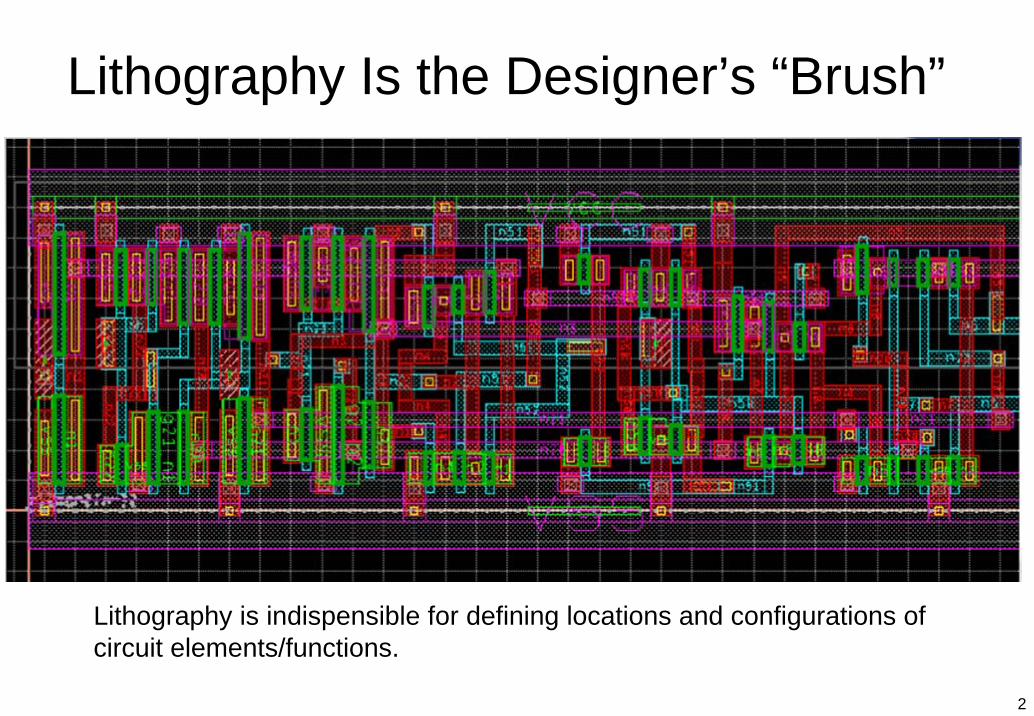
Lithography Is the Designer’s “Brush”
Lithography is indispensible for defining locations and configurations of circuit elements/functions.
3
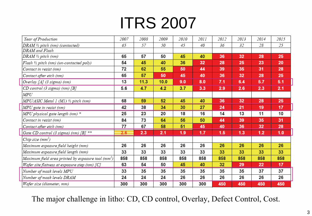
ITRS 2007
The major challenge in litho: CD, CD control, Overlay, Defect Control, Cost.

4
FSG
Metal 4 Copper
Passivation 1, USGPassivation 2, nitride
Lead-tin alloy bump
FSG
CopperMetal 2
FSG
FSG
CopperMetal 3
FSG
P-epiP-wafer
N-wellP-welln+STI p+ p+USGn+
PSG TungstenFSG
Cu Cu
Tantalum barrier layer
Nitride etch stop layer
Nitride seal layer
M 1
Tungsten local Interconnection
Tungsten plug
PMD nitride barrier layer
T/TiN barrier & adhesion layer
Tantalum barrier layer
Critical Layers
At least the following 4
• Active
• Gate
• Contact
• M1
5
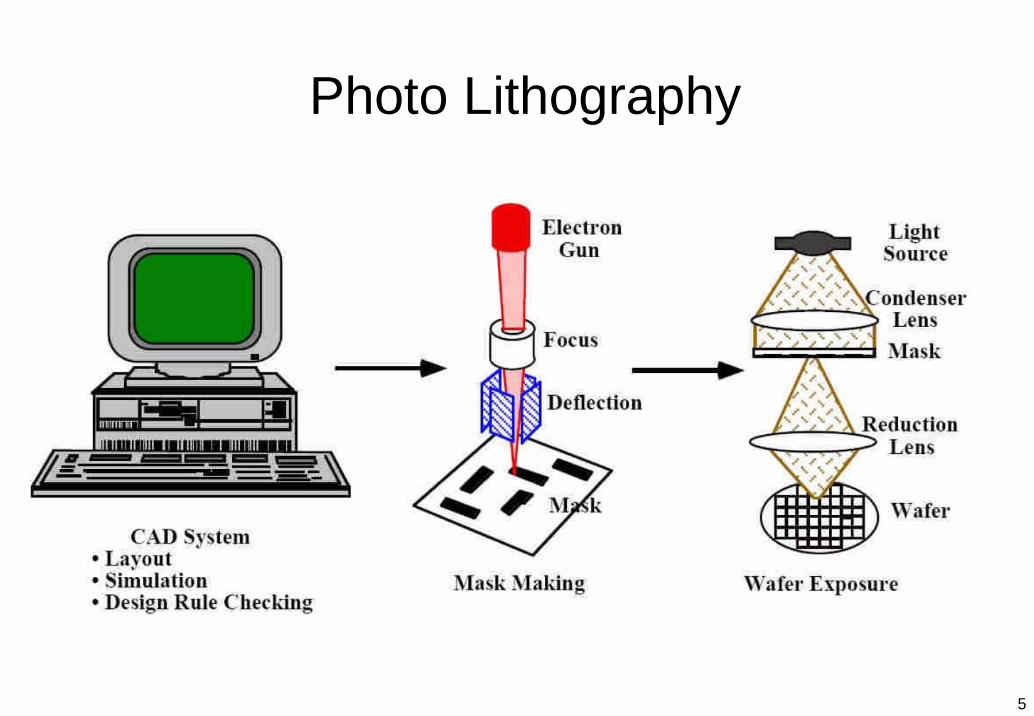
Photo Lithography

6
Photo Lithography
Photolithography is the patterning process that transfers the designed patterns from the mask to the resist on the wafer surface. It is the core of the manufacturing process flowProcess Sequence: photoresist coating, alignment and exposure, photoresist developingRequirements• High resolution• High sensitive• Precise alignment• Low defect density
High yield and good imaging

7
Photolithography Process
Substrate
Photoresist
Light Source
Mask Positive Resist
Alignment & ExposureResist Coating Developing

8
“Positive” and “Negative”Resist Processes
Mask/reticle
Exposure
UV light
Substrate
NegativePhotoresist
Substrate
PositivePhotoresist
Substrate
Photoresist
SubstratePhotoresist
After Development
Dr. Ko, Institute of Nanotechnology, NCTU
Positive PR: from insoluble to soluble Negative PR: from soluble to insoluble

9
PhotoresistPhotoresists are the photosensitive material coated temporarily on the wafer surface and used to transfer the image of designed circuit on the mask to the wafer surface The photosensitive chemical reaction (break bonds) mainly sensitive to the UV light and not sensitive to the visible light.Since resist is not sensitive to yellow light, all the fabs use yellow to illuminate lithography areas
Ingredients: polymer, solvent, sensitizer, additives
10
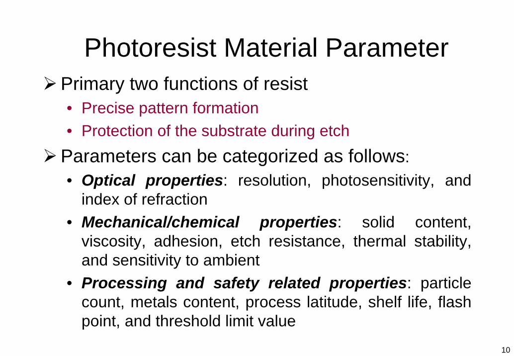
Photoresist Material ParameterPrimary two functions of resist• Precise pattern formation• Protection of the substrate during etch
Parameters can be categorized as follows:• Optical properties: resolution, photosensitivity, and
index of refraction• Mechanical/chemical properties: solid content,
viscosity, adhesion, etch resistance, thermal stability, and sensitivity to ambient
• Processing and safety related properties: particle count, metals content, process latitude, shelf life, flash point, and threshold limit value

11
Ingredients in I-line Resist• Polymer: Novolak
(Etch mask)
• Photoactive compound (PAC, or called sensitizer): diazonaphthoquinone (DNQ)
(Control photochemical reaction during exposure)
• Additive: phenolic materials
(Modify photochemical reaction during exposure)
• Solvent: PGMEA, EL
(Liquid suspension)H3C
O
CH2 C O
H
CH3
C
O
CH3
H3C C
H
OH
C
O
O C2H5Source:Prof. Ko in NCTU

12
Chemical Reaction in I-line Resist

13
Photo-ResistPositive PR• Becomes soluble after exposure• When developed, the exposed
parts dissolved• Better resolution
Negative PR• Exposed PR becomes cross-
linked polymer• Cross-linked polymer has higher
chemical etch resistance.• Becomes insoluble after
exposure• When developed, the unexposed
parts dissolved.• Cheaper material• Swelling lead to poor resolution
1
1
ln : ratioContrast −
⎥⎦
⎤⎢⎣
⎡⎟⎟⎠
⎞⎜⎜⎝
⎛≡
EETγ

14
Positive and Negative Resists
Azide/isoprene negative resist
Novolak resin resist
Swells during develop No swelling during develop
Marginal step coverage Good step coverage
Organic solvent developer Aqueous developer
Toxic strippers Environmentally benign resist stripper
Sensitive to ambient oxygen Operate well in air

15
DUV Resists• g-line and i-line resists have maximum quantum efficiencies < 1 and are
typically ≈ 0.3. • Chemical amplification can improve this substantially.• DUV resists all use this principle. A catalyst is used. • Photo-acid generator (PAG) is converted to an acid by photon exposure. Later,
in a post exposure bake, the acid molecule reacts with a “blocking” molecule on a polymer chain, making it soluble in developer AND REGENERATING THE ACID MOLECULE.
∴ catalytic action ∴ sensitivity is enhanced.
PAG
INSOL INSOL
Exposure
INSOL INSOL
Acid
Post ExposureBake (PEB)
SOL INSOL
Acid
SOL SOL
AcidAcid
a) b)
c)d)
Polymer Chain Polymer Chain
Polymer Chain Polymer Chain
Acid

16
MaskPhotoresist
Si Wafer
LightSource
OpticalSystem
Contact Printing Proximity Printing Projection Printing
Gap
1:1 Exposure Systems Usually 4X or 5XReduction
Wafer Exposure System

17
Projection Printing
Project an image of the mask pattern onto a resist coated wafer several centimeters away from the mask.• 1:1 projection optical system is easier to
design.• M:1 projection mask is easier to fabricate
(5:1 most common or 10:1).
Projection method• Scan• Step-and-repeat• Step-and-scan
Light Source
Lens
Mask
Photoresist
Wafer
Synchronized mask and wafer movement
Slit
Lens
Wafer Stage
ProjectionLens
LightSource
Reticle
Wafer
ProjectionLens
Scan
Step and repeat

18
Lens Field Size Overlay ThroughputNA Resolution Max X & Y 2 pt. Global
Alignment200 mm Wafers
70 Exp., 200 mJ/cm2
Variable0.48 to 0.60
< 280 nm 22 X 27.4 mm < 40 nm > 100 wph
I-Line Stepper
19
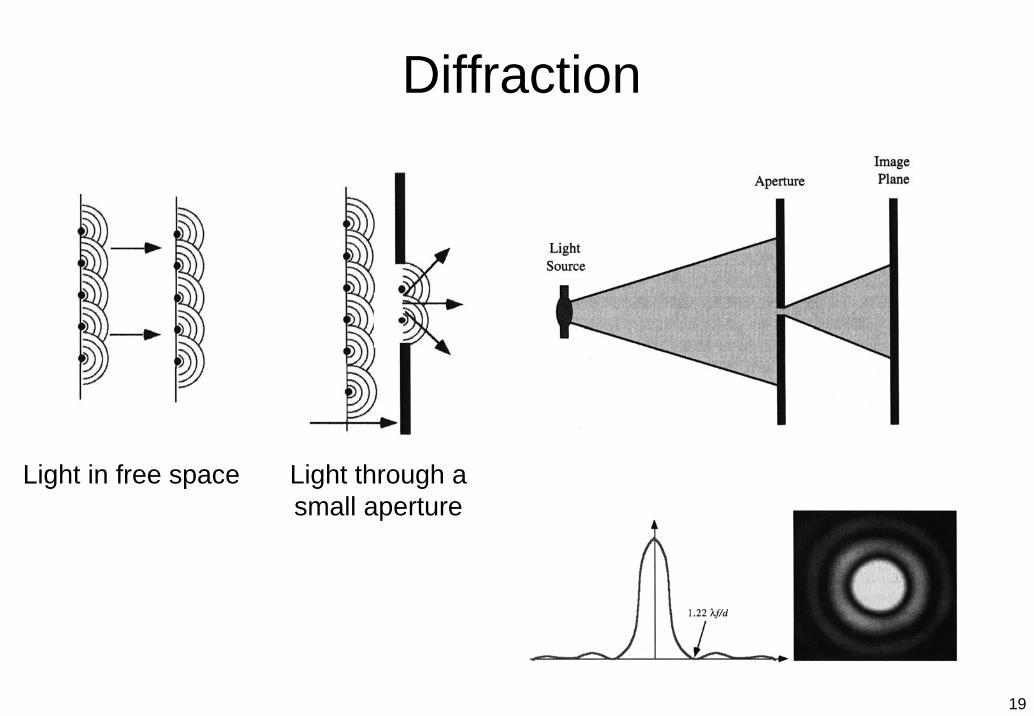
Diffraction
Light in free space Light through a small aperture

20
Fresnel Diffraction
WaferResist MaskAperture
Incident Plane Wave
Light Intensityat Resist Surface
g
W
λ < g < W2
λFresnel diffraction (near-field diffraction) applies when
Within this range, the minimum resolvable feature size is Wmin ≈ λg
Thus if g = 10 µm and an i-line (365nm) light source is used, Wmin ≈ ??

21
Shadowing Printing
Contact printing• Resolution ~ 1um• Dust on mask will damage PR pattern.• Mask pattern may be contaminated.
Proximity printing• A small gap of 10-50 um.• Longer mask lifetime.• Poorer resolution.
gapR ×= λ

22
Fraunhofer DiffractionImagePlane
PointSources d
AB
A'
B'
α
EntranceAperture
Fraunhofer diffraction (far-field diffraction) is dominate in the projection system. According to the Rayleigh Criterion:
R
1.22 1.22 0.61 (2 sin ) sin
f fRd n f nλ λ λ
α α= = =

23
Resolution1
KRN Aλ
= λ: wavelength, K1 : system constant=0.61 (ideal)NA = n sinα= d/2f
NA (numerical aperture): the capability of the lens to collect the diffraction light. NA is proportional to the lens diameter (camera with large lens) and reversely proportional to the distance between the wafer and the lens.
Diffracted light collected by the lens
Strayed refracted light
Lens
Ideal light Intensity pattern
Less diffraction after focused by the lens
Mask
ro
D
24
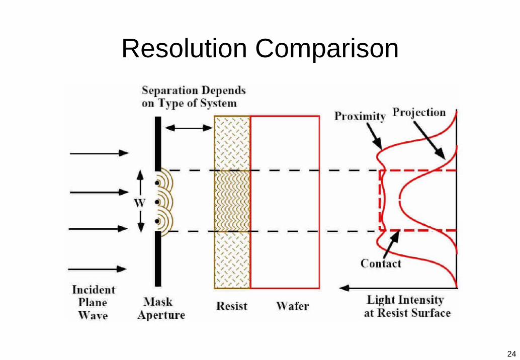
Resolution Comparison
25
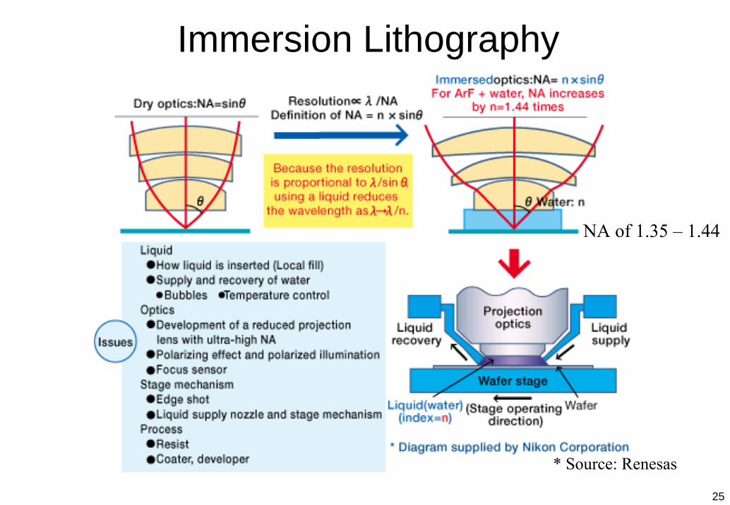
* Source: Renesas
Immersion Lithography
NA of 1.35 – 1.44

26
22( )
KDOFNA
λ= NA : numerical aperture, λ : wavelength, K2 : system constant =0.5 (ideal)
DOF
Depth of Focus
Lens
Ex: Point and shot cameras use small lens without focus but the resolution won’t be great!
Very flat wafer surface is needed -> CMP
PhotoresistSubstrate
Depth of focusCenter of focus
27
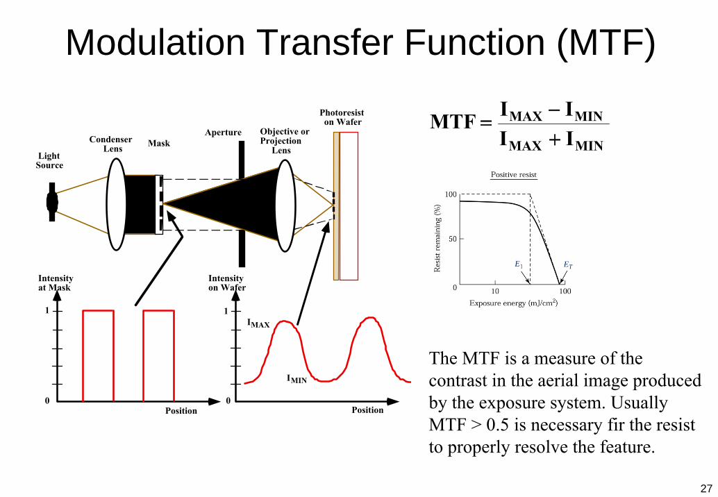
Modulation Transfer Function (MTF)
MTF = IMAX − IMIN
IMAX + IMIN
Intensityat Mask
Intensityon Wafer
0
1
0
1IMAX
IMIN
Aperture
LightSource
Condenser Lens
Objective orProjection Lens
Photoresist on Wafer
Mask
Position Position
The MTF is a measure of the contrast in the aerial image produced by the exposure system. Usually MTF > 0.5 is necessary fir the resist to properly resolve the feature.
28
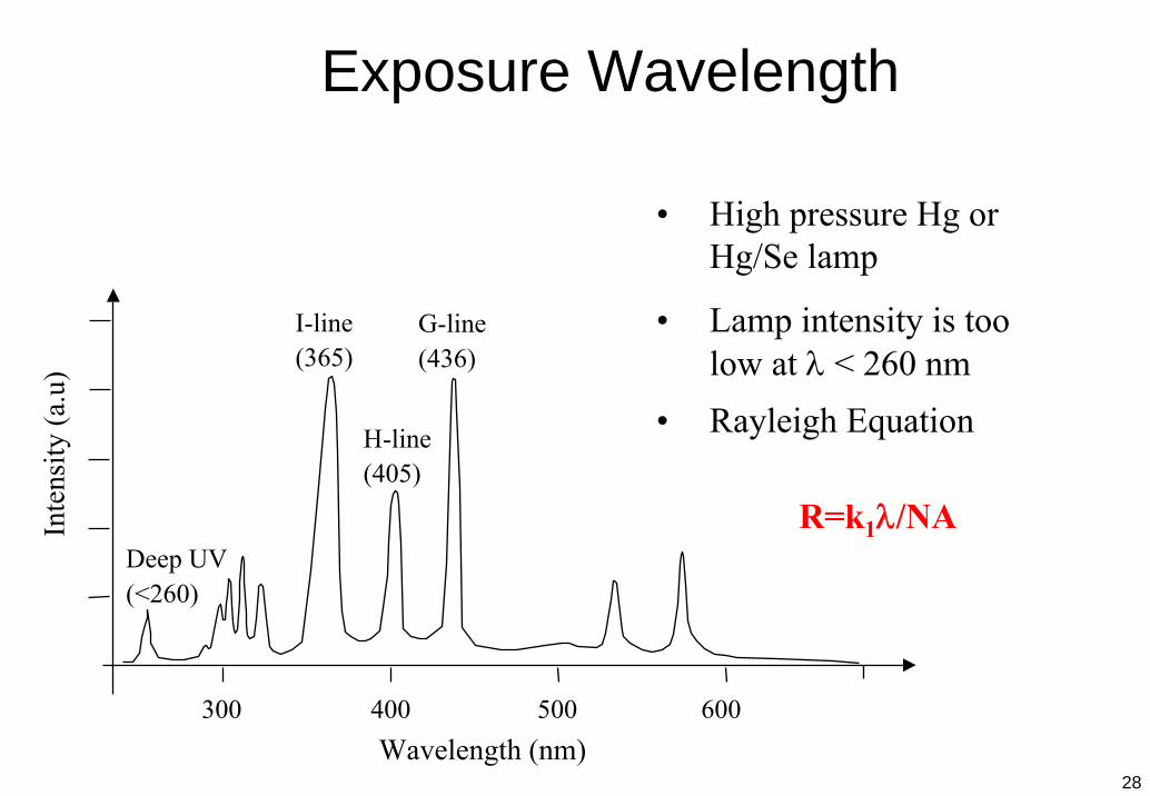
Exposure Wavelength
G-line(436)
H-line(405)
I-line(365)
300 400 500 600Wavelength (nm)
Inte
nsity
(a.u
)
Deep UV(<260)
• High pressure Hg or Hg/Se lamp
• Lamp intensity is too low at λ < 260 nm
R=k1λ/NA
• Rayleigh Equation

29
Exposure Wavelength
30
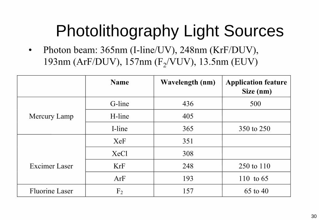
• Photon beam: 365nm (I-line/UV), 248nm (KrF/DUV), 193nm (ArF/DUV), 157nm (F2/VUV), 13.5nm (EUV)
Name Wavelength (nm) Application feature Size (nm)
G-line 436 500
Mercury Lamp H-line 405
I-line 365 350 to 250
XeF 351
XeCl 308
Excimer Laser KrF 248 250 to 110
ArF 193 110 to 65
Fluorine Laser F2 157 65 to 40
Photolithography Light Sources

31
Pre-baking• 90-120°C for 60-120 sec.
Adhesion promoter vapor deposition or spin coatingPR spin coater• 3000-6000 RPM for 1um• with edge bead remove
Soft baking• 90-120°C for 60-120 sec.
ExposurePost exposure baking (PEB)• ~100°C for 10 min.
PR DevelopingHard baking• 100-180°C for 10-30 min.
Photolithography Process

32
Wafer Clean
P-Well
USGSTIPolysilicon
Gate Oxide
Wafer Clean
• Removing all contaminants from the surface
• Standard cleaning process can remove particle, organic and metal
• The native oxide can be removed by dipping in diluted HF
• Improved adhesion
Dr. Ko, Institute of Nanotechnology, NCTU
33
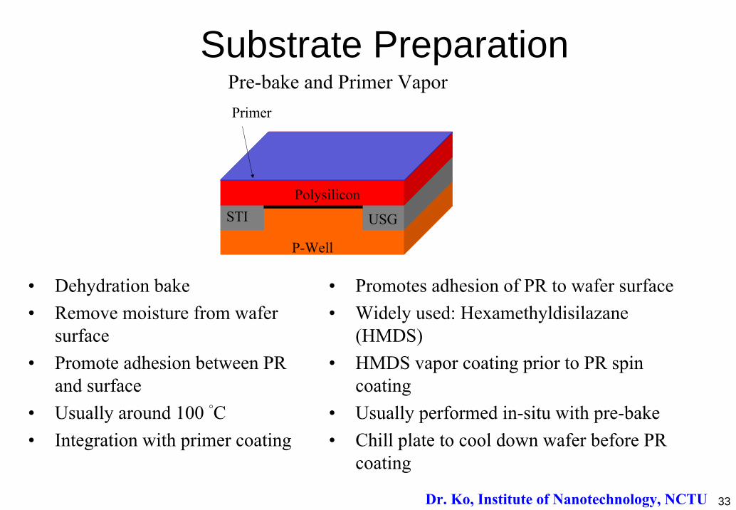
• Promotes adhesion of PR to wafer surface• Widely used: Hexamethyldisilazane
(HMDS) • HMDS vapor coating prior to PR spin
coating• Usually performed in-situ with pre-bake• Chill plate to cool down wafer before PR
coating
Pre-bake and Primer Vapor
P-Well
USGSTIPolysilicon
Primer
Substrate Preparation
• Dehydration bake• Remove moisture from wafer
surface • Promote adhesion between PR
and surface• Usually around 100 ˚C• Integration with primer coating
Dr. Ko, Institute of Nanotechnology, NCTU

34
Primer Vapor CoatingDehydration Bake
Wafer
Prep Chamber Primer Layer
Wafer
Hot Plate Hot Plate
HMDS Vapor
Si Si晶圓表面
Si Si親水性表面
OH OH
H 3CH 3C–Si–N–Si–CH 3
H 3C CH 3
CH 3
H
Si Si疏水性表面
O OSiSi
H 3CH 3C CH 3 CH 3
CH 3H 3C+ H 2O + NH 3
Substrate Preparation
Dr. Ko, Institute of Nanotechnology, NCTU

35
Resist Coating
P-Well
USGSTIPolysilicon
Photoresist
Primer
• Wafer sits on a vacuum chuck• Liquid photoresist applies at center of wafer• Rotate at high speed• Photoresist spreads by centrifugal force• Evenly coat on wafer surface
Dr. Ko, Institute of Nanotechnology, NCTU

36
Resist Spin Coater

37
• Photoresist spread on spinning wafer surface
• Wafer held on a vacuum chuck• Slow spin ~ 500 rpm• Ramp up to ~ 3000 - 7000 rpm
Dynamic Spin RateResist Thickness
Viscosity Effect

38
Resist Spin Coater

39
Soft Baking
• Hot plate heating is widely used• Evaporating most of solvents from PR film (5~20 % left)• Solvents help to make a thin PR but absorb radiation and affect
adhesion• Soft baking time and temperature are determined by the matrix
evaluations• Over bake: polymerized, less photo-sensitivity• Under bake: affect adhesion and exposure (solvent is not sensitive)
Dr. Ko, Institute of Nanotechnology, NCTU
40
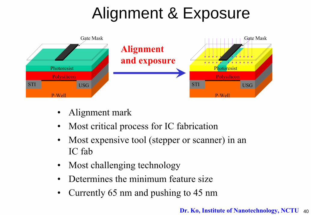
Alignment & Exposure
P-Well
USGSTIPolysilicon
Photoresist
Gate Mask Gate Mask
P-Well
USGSTIPolysilicon
Photoresist
Alignment and exposure
• Alignment mark • Most critical process for IC fabrication• Most expensive tool (stepper or scanner) in an
IC fab• Most challenging technology• Determines the minimum feature size• Currently 65 nm and pushing to 45 nm
Dr. Ko, Institute of Nanotechnology, NCTU

41
Structure of Mask
quartz
Cr2O3
Cr
Cr2O3, 30nm
Cr, 70nm
quartz, 2.3mm
Electron beam lithography
Which illumination mode is correct ?
Dr. Ko, Institute of Nanotechnology, NCTU
42
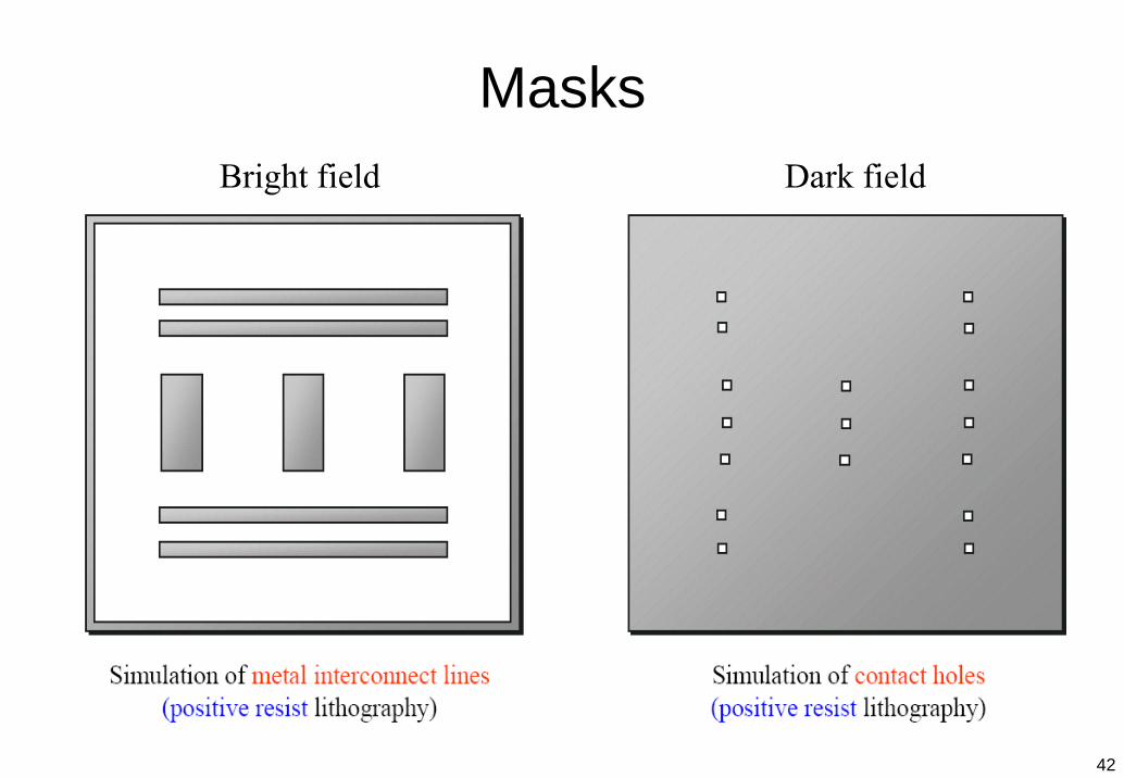
MasksBright field Dark field

43
Post Exposure Baking
P-Well
USGSTIPolysilicon
Photoresist
• Photoresist has glass transition temperature (Tg)• Baking temperature higher than Tg
• Thermal movement of photoresist molecules• Rearrangement of the overexposed and underexposed
PR molecules• Average out standing wave effect• Smooth PR sidewall and improve resolution
Photoresist
λ/2nPR
Substrate
OverexposureUnderexposure
Photoresist
λ/2nPR
Substrate
OverexposureUnderexposure
Dr. Ko, Institute of Nanotechnology, NCTU

44
45
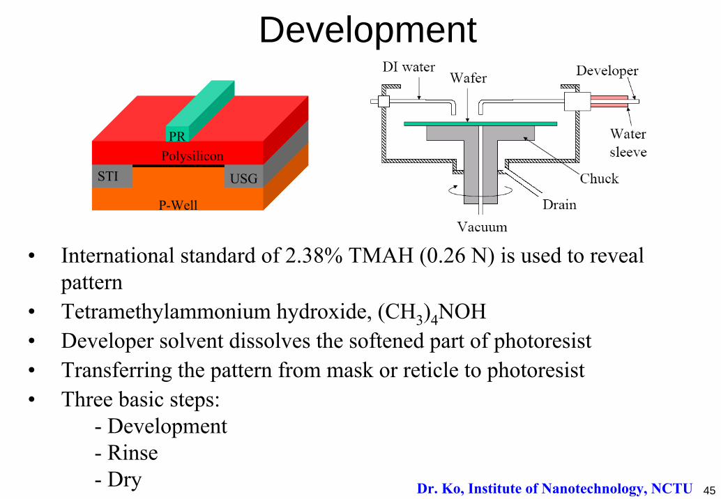
Development
P-Well
USGSTIPolysilicon
PR
• International standard of 2.38% TMAH (0.26 N) is used to reveal pattern
• Tetramethylammonium hydroxide, (CH3)4NOH• Developer solvent dissolves the softened part of photoresist• Transferring the pattern from mask or reticle to photoresist• Three basic steps:
- Development- Rinse- Dry Dr. Ko, Institute of Nanotechnology, NCTU

46

47
Development

48
Hard Baking
P-Well
USGSTIPolysilicon
PR
Evaporating all solvents in PRImproving etch and implantation resistanceImprove PR adhesion with surfacePolymerize and stabilize photoresistPR flow to fill pinholeUnder-bake • Photoresist is not fully
polymerized• High photoresist etch rate • Poor adhesion
Over-baking • PR flow and bad resolution
Dr. Ko, Institute of Nanotechnology, NCTU

49
Hard Baking

50
P-Well
USGSTIPolysilicon
PR
Pattern Inspection
• Inspection: go next step or rework (stripping PR)– Photoresist pattern is temporary – Etch or ion implantation pattern is permanent
• Photolithography process can rework • Can’t rework after etch or implantation • Scanning electron microscope (SEM) • Optical microscope (OM)
Dr. Ko, Institute of Nanotechnology, NCTU
51
Pattern Inspection
Overlay or alignment• run-out, run-in, reticle rotation, wafer rotation,
misplacement in X-direction, and misplacement in Y-direction
Critical dimension (CD)Surface irregularities such as scratches, pinholes, stains, contamination, etc.
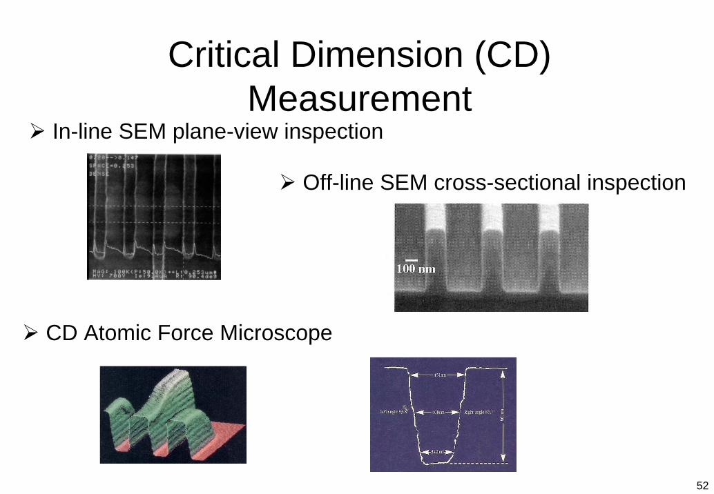
52
Critical Dimension (CD) Measurement
Off-line SEM cross-sectional inspection
In-line SEM plane-view inspection
CD Atomic Force Microscope

53
Critical Dimension (CD)

54
Misalignment
55
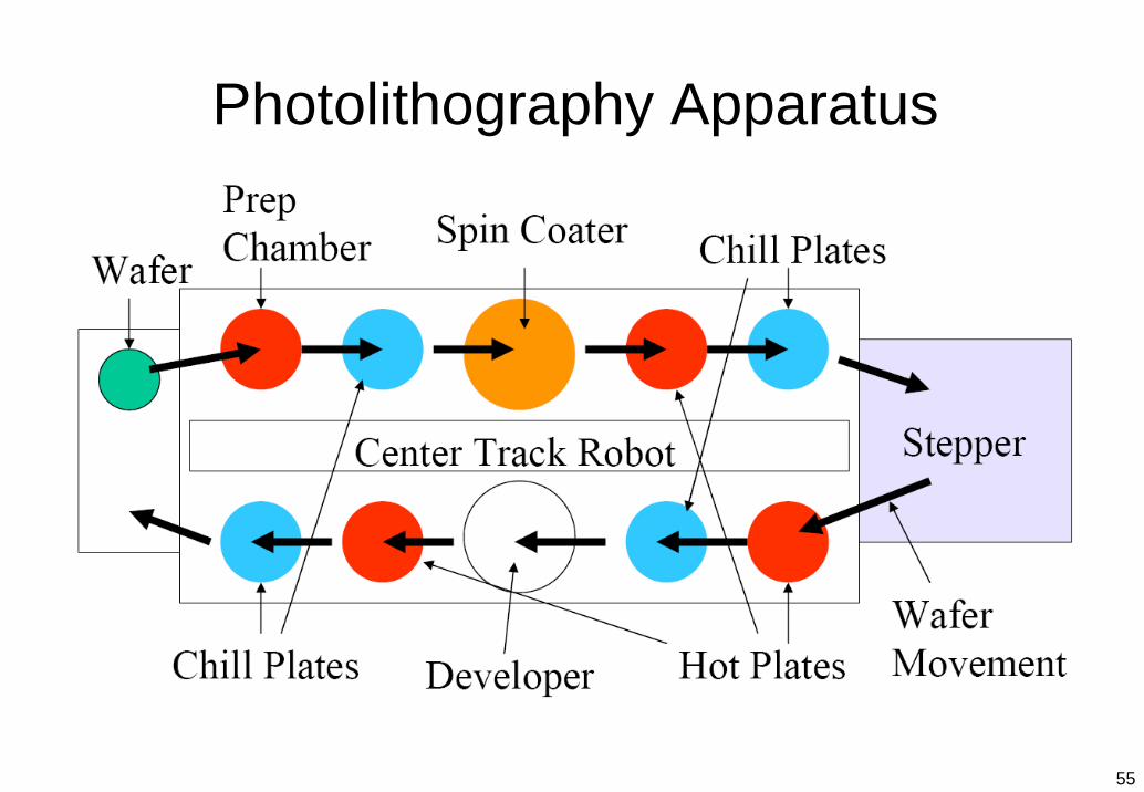
Photolithography Apparatus

56
Process Flow Chart
57
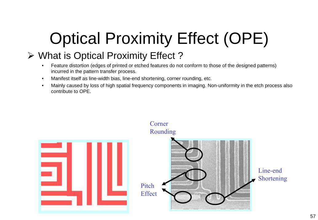
Optical Proximity Effect (OPE)What is Optical Proximity Effect ?
• Feature distortion (edges of printed or etched features do not conform to those of the designed patterns) incurred in the pattern transfer process.
• Manifest itself as line-width bias, line-end shortening, corner rounding, etc.• Mainly caused by loss of high spatial frequency components in imaging. Non-uniformity in the etch process also
contribute to OPE.
Line-endShortening
PitchEffect
CornerRounding

58
Optical Proximity Correction (OPC)How to Minimize OPE ?
• Pre-distort the patterns on the mask to minimize OPE.
On wafer
On mask
Before OPC After OPCOptical effect
After OPCInclude PR process

59
Example of OPC
Before OPC
After OPC
On Focus Defocus
SEM picturesOn mask

60
Phase Shift Mask
61
Advanced Lithography
E-beam lithography
X-ray lithography
Extreme UV (EUV) lithography
Nanoimprint

62
E-Beam Lithography
W or LaB6 thermionic-emission tip
Focus beam diameter to 10-25 nm
Turn on/off beam
Computer controlled to direct the beam. Scan field ~ 1cm
Advantages : High resolution~30nm, Large DOF~20-30um, Maskless

63
Evolution of e-Beam System

64
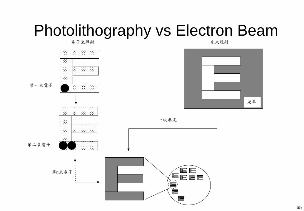
65
Photolithography vs Electron Beam電子束照射
第一束電子
第二束電子
第n束電子
光束照射
光罩
一次曝光

66
SCALPEL

67
X-Ray Lithography (XRL)
Tool feature• Energy ~ 1-10 KeV• Wave length ~ 1nm• 1:1 proximity exposure
Advantages• High resolution• No reflection
Disadvantages• X-ray source (Synchrotron source)• Mask fabrication

68
XRL MaskXRL mask
• No materials transmit X-rays easily.• The clear areas need to be made from thin layers of low mass materials such as Si,
Si3N4, SiC or BN of a few um thick.• The dark areas are made from heavy atoms such as W, Ta, or Au of about 0.5um
thick.• Mask absorbs 25%-35% of the incident flux and must be cooled.

69
EUV System

70
Light Source

71

72
Nano Imprint Lithography