
Random Testing of Asynchronous VLSI...
140
Random Testing of Asynchronous VLSI Circuits A thesis submitted to the University of Manchester for the degree of Master of Science in the Faculty of Science Oleg Alexandrovich Petlin Department of Computer Science 1994
Transcript of Random Testing of Asynchronous VLSI...

Random Testing of
Asynchronous VLSI Circuits
A thesis submitted to the University of
Manchester for the degree of Master of
Science in the Faculty of Science
Oleg Alexandrovich Petlin
Department of Computer Science
1994
Page 2
Contents
Contents................................................................................................ 2List of Figures ...................................................................................... 5List of Tables........................................................................................ 8Abstract ................................................................................................ 9
Chapter 1 : Asynchronous VLSI designs ...........................................13
1.1 Asynchronous versus synchronous VLSI circuits...................................131.2 Asynchronous design...............................................................................151.3 Transition signalling................................................................................161.4 Event-controlled logic elements ..............................................................191.5 Asynchronous micropipelines .................................................................201.6 Summary..................................................................................................23
Chapter 2 : Testing VLSI circuits ......................................................24
2.1 Problems in testing VLSI circuits............................................................242.2 Fault models for VLSI circuits ................................................................252.3 Logic testing of VLSI circuits .................................................................28
2.3.1 Test generation methods .................................................................. 292.3.2 Response evaluation techniques ...................................................... 33
Chapter 3 : Pseudo-random testing of VLSI circuits .........................36
3.1 Generating pseudo-random patterns........................................................363.2 Exhaustive and pseudo-exhaustive testing of VLSI circuits ...................423.3 Signature analysis....................................................................................44
Chapter 4 : Design for testability of VLSI circuits ............................48
4.1 What is design for testability? .................................................................484.2 Ad-hoc techniques ...................................................................................494.3 Structured approaches .............................................................................51
4.3.1 Scan path.......................................................................................... 524.3.2 Level-sensitive scan design ............................................................. 534.3.3 Scan/set technique ........................................................................... 554.3.4 Random access scan ........................................................................ 56
4.4 Built-in self-test .......................................................................................57

Contents
Page 3
4.4.1 InSitu self-testing............................................................................. 584.4.2 ExSitu self-testing............................................................................ 61
4.5 Summary..................................................................................................63
Chapter 5 : Testing asynchronous VLSI designs - related works ......65
5.1 Problems with testing asynchronous VLSI circuits.................................655.2 Testing bounded-delay circuits................................................................665.3 Testing delay-insensitive circuits ............................................................755.4 Testing speed-independent networks ......................................................775.5 Testing micropipelines ............................................................................78
Chapter 6 : Asynchronous random testing interface ..........................82
6.1 Asynchronous implementations of PRPG and signature analyser ..........826.1.1 Asynchronous PRPG ....................................................................... 836.1.2 Asynchronous signature analyser .................................................... 84
6.2 Generating patterns for the random testing of asynchronous VLSIcircuits .....................................................................................................85
6.2.1 Generating equiprobable test patterns ............................................. 856.2.2 A PRPG for weighted test patterns.................................................. 91
6.3 Program tools for the behavioural simulation of PRPGs ........................92
Chapter 7 : Test lengths for random testing of micropipelines ..........96
7.1 Test length for random pattern testing.....................................................977.2 Test length for random testing using weighted patterns........................1037.3 Summary................................................................................................110
Chapter 8 : Special aspects of random testing of asynchronouscircuits...........................................................................111
8.1 Probabilistic properties of the Muller-C element ..................................1118.2 Random testing of asynchronous control circuits .................................114
8.2.1 Random testing of the Muller-C element ...................................... 1148.2.2 Random testing of a certain class of asynchronous circuits .......... 116
8.3 Generating patterns for the pseudo-random testing of micropipelinesand asynchronous control circuits .........................................................122
Chapter 9 : Conclusions and further work .......................................125
9.1 Conclusions ...........................................................................................1259.2 Future work ...........................................................................................128
Appendix A : Asynchronous 4-bit PRPG ....................................... 130

Contents
Page 4
A.1 Schematic of the generator .................................................................. 130A.2 The register of the generator................................................................ 131A.3 Simulation results ................................................................................ 132
Appendix B : Asynchronous 4-bit parallel signature analyser........ 133
B.1 Schematic of the signature analyser..................................................... 133B.2 The register of the signature analyser .................................................. 134B.3 Simulation results ................................................................................ 135
References ........................................................................................ 136

Page 5
List of Figures
Figure 1.1: The standard bundled data interface....................................................17
Figure 1.2: Two-phase transition signaling............................................................18
Figure 1.3: Four-phase transition signaling ...........................................................18
Figure 1.4: An assembly of basic logic modules for events ..................................20
Figure 1.5: A computation micropipeline ..............................................................21
Figure 1.6: An asynchronous sequential circuit.....................................................22
Figure 2.1: NMOS NOR gate with four faults.......................................................26
Figure 2.2: Delay fault hazard in an asynchronous VLSI circuit...........................28
Figure 2.3: VLSI logic testing................................................................................29
Figure 2.4: Path sensitization technique ................................................................31
Figure 2.5: Stored response testing ........................................................................33
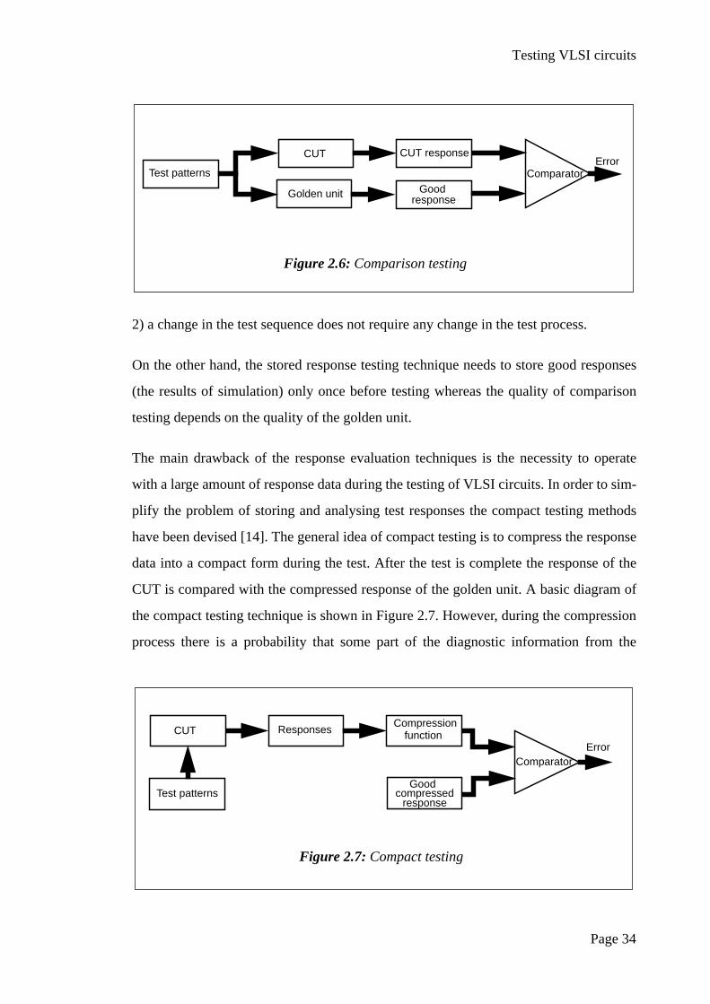
Figure 2.6: Comparison testing..............................................................................34
Figure 2.7: Compact testing ...................................................................................34
Figure 3.1: Linear feedback shift register ..............................................................37
Figure 3.2: Modular realization of a LFSR............................................................37
Figure 3.3: Four-bit PRPG.....................................................................................38
Figure 3.4: A modified four-stage LFSR...............................................................43
Figure 3.5: General structure of a signature analyser ............................................45
Figure 3.6: Four-stage serial signature analyser ....................................................45
Figure 3.7: Four-stage parallel signature analyser .................................................46
Figure 4.1: Improving VLSI testability using (a) demultiplexers; (b) multi-plexers ..................................................................................................49
Figure 4.2: Using shift registers for improving (a) control access; (b) obser-vation access ........................................................................................50
Figure 4.3: Huffman model for a sequential circuit...............................................51
Figure 4.4: The principle of scan path techniques .................................................52
Figure 4.5: Polarity hold latch (a) symbolic representation; (b) implementa-tion in NAND gates..............................................................................53
Figure 4.6: LSSD structure ....................................................................................54
Figure 4.7: Scan/Set configuration.........................................................................55
Figure 4.8: Random access scan structure .............................................................56

List of Figures
Page 6
Figure 4.9: Taxonomy of self-test approaches.......................................................57
Figure 4.10: Basic BILBO element........................................................................58
Figure 4.11: Self-testing structure with BILBOs...................................................59
Figure 4.12: ExSitu self-testing structure ..............................................................61
Figure 4.13: LOCST test structure.........................................................................61
Figure 4.14: ExSitu STUMPS approach................................................................63
Figure 5.1: Modifying sequential circuit S into a) its acyclic counterpart; b)corresponding iterative combinational circuit .....................................67
Figure 5.2: R-S flip-flop realized using NAND gates ...........................................69
Figure 5.3: Equations for handling faults in a NAND circuit for the case ofa) stuck-at-0 fault at the output; b) stuck-at-1 fault at input a..............70
Figure 5.4: An example of untestable a) and testable b) asynchronous resetnetwork.................................................................................................72
Figure 5.5: Testing asynchronous reset network: a) synchronous model; b)asynchronous model.............................................................................72
Figure 5.6: Event controlled latch..........................................................................80
Figure 6.1: Asynchronous random testing interface with the two-phase bun-dled data convention ............................................................................83
Figure 6.2: An asynchronous version of a pseudo-random pattern genera-tor .........................................................................................................83
Figure 6.3: An asynchronous implementation of a signature analyser ..................85
Figure 6.4: Asynchronous logic with a latch .........................................................86
Figure 6.5: An example of asynchronous circuit with undetectable faults............87
Figure 6.6: The 6-bit PRPG based on using the 8-th state from the state mod-ification table of the 6-bit LSFR ..........................................................90
Figure 6.7: A general structure of a PRPG with given signal probabilities onits outputs .............................................................................................91
Figure 6.8: A general structure of the universal PRPG..........................................93
Figure 6.9: A WPRPG built by using ROMs.........................................................94
Figure 6.10: A PRPG of weighted patterns based on using additional logicelements ...............................................................................................95
Figure 7.1: Random testing of logic blocks of micropipelines ..............................97
Figure 7.2: Random testing a combinational logic block. .....................................98
Figure 7.3: The Markov chain describing the process of the appearance oftwo different random patterns ............................................................104
Figure 7.4: A graph of the dependence between the relative error and theescape probability .............................................................................108
Figure 8.1: An implementation of the two-input Muller-C element....................111
List of Figures
Page 7
Figure 8.2: An example of an asynchronous logic block.....................................117
Figure 8.3: An asynchronous logic circuit for random pattern testability ...........120
Figure 8.4: PRPG used for testing micropipelines...............................................122
Figure A.1: An asynchronous implementation of the 4-bit PRPG ......................130
Figure A.2: An implementation of the 4-bit register of the generator .................131
Figure A.3: The results of the behavioural simulation of the generator ..............132
Figure B.1: An asynchronous implementation of the 4-bit parallel signatureanalyser .............................................................................................133
Figure B.2: An implementation of the register of the signature analyser ............134
Figure B.3: The results of the behavioural simulation of the signature ana-lyser...................................................................................................135

Page 8
List of Tables
Table 2.1: The truth table of NMOS NOR gate with four faults ...........................26
Table 3.1: State sequence for the four-bit PRPG...................................................39
Table 3.2: Primitive polynomials for different n from 1 to 33 ..............................41
Table 5.1: Equations for an R-S flip-flop ..............................................................70
Table 6.1: State modifying table for the 4-bit LFSR .............................................87
Table 6.2: State sequence for the four-bit PRPG built using the statemodification procedure.........................................................................88
Table 6.3: Table of equivalence between states of the three 4-bitPRPGs...................................................................................................89
Table 6.4: State modifying table for the 6-bit LFSR .............................................90
Table 7.1: Statistical and theoretical random lengths for the exhaustivetesting of combinational networks......................................................102
Table 7.2: Numerical solutions of inequalities (17) and (18) ..............................107
Table 7.3: Theoretical and experimental results for estimating the testlengths for random pattern testing of a 3-inputcombinational circuit .........................................................................109
Table 8.1: Equations for calculating theoretical probabilities of a oneand zero of basic logic elements.........................................................120
Table 8.2: State sequence for the two-bit PRPG..................................................123
Page 9
Abstract
Asynchronous VLSI designs are becoming an intensive area of research due to their
advantages in comparison with synchronous circuits, such as the absence of the clock
distribution problem, lower power consumption and higher performance.
The work described in this thesis is an attempt to find possible ways to test asynchro-
nous VLSI circuits using random (or, more accurately, pseudo-random) patterns. The
main results have been obtained in the field of random testing of stuck-at faults in micro-
pipelines.
An asynchronous random testing interface has been designed which includes an asyn-
chronous pseudo-random pattern generator and an asynchronous parallel signature ana-
lyser. A program model of the universal pseudo-random pattern generator has been
developed. The universal pseudo-random pattern generator can produce multi-bit
pseudo-random sequences without an obvious shift operation and it can also produce
weighted pseudo-random test patterns.
Mathematical expressions have been derived for predicting the test length for random
pattern testing of logic blocks of micropipelines by applying equiprobable and weighted
random patterns to the inputs.
The probabilistic properties of then-input Muller-C element have been investigated. It is
shown that the optimal random test procedure for then-input Muller-C element is ran-
dom testing using equiprobable input signals. Using the probabilistic properties of the
Muller-C element and multiplexers incorporated into the circuit a certain class of asyn-
chronous networks can be designed for random pattern testability. It is also shown how
it is possible to produce pseudo-random patterns to detect all stuck-at faults in micropi-
pelines.

Page 10
Declaration
No portion of the work referred to in this thesis has been submitted in support of an
application for another degree or qualification of this or any other university or institute
of learning.
Copyright in text of this thesis rests with the Author. Copies (by any process) either in
full, or of extracts, may be madeonly in accordance with instructions given by the
Author and lodged in the John Rylands University Library of Manchester. Details may
be obtained from the Librarian. This page must form part of any such copies made. Fur-
ther copies (by any process) of copies made in accordance with such instructions may
not be made without the permission (in writing) of the Author.
The ownership of any intellectual property rights which may be described in this thesis
is vested in the University of Manchester, subject to any prior agreements to the con-
trary, and may not be made available for use by third parties without the written permis-
sion of the University, which will prescribe the terms and conditions of any such
agreement.
Further information on the conditions under which disclosures and exploitation may
take place is available from the Head of Department of Computer Science.

Page 11
Acknowledgements
During the last year I have received a great help from many people, without which the
work described in this thesis would have been very difficult or even impossible.
My supervisor Professor Steve Furber has been a great source of inspiration and moral
support. I would like to express my gratitude for his constant interest in my ideas and
research results and for correcting and commenting on drafts of this thesis.
The other members of the AMULET research group have created a very friendly and
comfortable atmosphere for me to lead my research. I would like to thank all of those
people who have spent their valuable time to help me to understand asynchronous VLSI
designs.
I am especially grateful to Phil Endecott for his help and useful tips with GCC and
FrameMaker, and Dr. Jim Garside for providing assistance with Powerview CAD tools.
Some people have helped by reading and commenting on drafts of this thesis as well. I
must express my thanks to Phil Endecott for his useful comments.

Page 12
The Author
Oleg Petlin obtained an Engineer degree (1989) and a Candidate of Technical Sciences
degree (1993) in Computer Science from Kiev Polytechnical Institute (Ukraine). This
thesis is the result of the first year of research as a member of the AMULET research
group at the University of Manchester.
AMULET (Asynchronous Microprocessor Using Low Energy Techniques) comprises
four projects looking at different areas where asynchronous logic techniques can be
applied.
Page 13
Chapter 1 : Asynchronous VLSI
designs
1.1 Asynchronous versus synchronous VLSI circuits
The combination of recent developments in the technology for producing digital circuits
with powerful computer-aided design (CAD) tools [1, 2] has given designers new
opportunities to create circuits with high performance and high density of logic elements
in the form of very large scale integrated (VLSI) circuits.
Almost all today’s VLSI circuits and systems are designed using two major conceptual
rules: information is represented in a binary format, and time is discrete. In general, this
is an artificial approach to designing digital circuits which is used because it avoids
many of the problems concerned with representing and processing digital information.
Usually such VLSI circuits use a common clock signal distributed through the design to
control the timing and sequencing of the data flow. In such synchronous VLSI circuits,
hazards can be ignored simplifying the digital design process.
A VLSI circuit is a system of a large number of interconnected elements where a
sequence of events is realized. The most natural discipline for processing information in
digital systems is asynchronous, i.e. each element processes data in response to new
information being delivered to its inputs. The combination of an asynchronous disci-
pline for controlling the sequence of handling digital information with VLSI technology
creates new possibilities for designing VLSI circuits with new features and advantages
[3, 4, 5, 6, 7]. There are some general benefits of using asynchronous designs in compar-
ison with synchronous ones:
• The clock skew problem. The clock skew problem appears when it is necessary to
synchronize different parts of a VLSI system. This synchronization cannot be com-
pletely accurate for the simple reason the clock signal arrives at different parts of the
Asynchronous VLSI designs
Page 14
VLSI circuit at different times, due to different track lengths. Asynchronous circuits
by definition have no common clock and, therefore, have no clock skew problem.
• Metastability problem. It is known that for a successful computation process the data
must be valid before being clocked. If this condition is not obeyed a synchronous cir-
cuit can go into an unstable equilibrium which is called a metastable state. Thus, the
exact values of the delays of elements must be known to ensure correct synchroniza-
tion. Asynchronous elements can have arbitrary delays and can wait an arbitrary time
while input information stabilizes.
• Performance. The performance of synchronous VLSI systems is limited by the worst
case when an element processes information for the longest time. As a rule, this situ-
ation is rare but must be taken into account to avoid the metastability problem. Asyn-
chronous VLSI circuits operate at a rate determined by element and wiring delays. As
a result the performance rate tends to reflect the average case delay rather than the
worst case delay.
• Power consumption. Synchronous VLSI circuits are designed in such way that even
if some parts of the circuit are not involved in a computation process they have to be
clocked, i.e. they perform their functions with data which is not in use. In contrast, in
asynchronous VLSI designs only those parts of the circuit which produce “useful”
information take part in the computation. This property of asynchronous designs
leads to power savings in VLSI circuits.
• Timing and design flexibility. If a designer of a synchronous VLSI circuit is required
to make a circuit work at a higher clock frequency, all parts of the circuit must be
improved because of the worst-case performance property. In the case of asynchro-
nous designs the problem can be solved if only “the most active” parts of the circuits
are modified. These modifications can be implemented using new developments in
VLSI technology. In general, greater throughput for synchronous circuits can be
achieved only when all VLSI components are realized on a new technology because
the critical (longest) path can go through all the elements of the VLSI circuit.

Asynchronous VLSI designs
Page 15
Besides the advantages, asynchronous circuits also have some disadvantages. It appears
to be difficult to design asynchronous VLSI circuits for specific applications. The
designers must pay great attention to the dynamic properties of asynchronous circuits
and to the control of the sequence of operations. The lack of powerful CAD tools makes
it difficult to design asynchronous VLSI circuits. Nevertheless, the scope of asynchro-
nous designs is wider than that of synchronous ones. This encourages designers to do
more research in the field of creating productive asynchronous VLSI circuits.
1.2 Asynchronous design
In general synchronous designs can be seen as a particular case of representing data
processing designs in the multi-dimensional asynchronous world [2]. There are many
different approaches to designing asynchronous VLSI circuits. Nevertheless, the most
popular design approaches currently in use can be categorized by the way data is repre-
sented and processed [4]:
• Data representation. Data in asynchronous designs can be represented either by using
a dual rail encoding technique or a data bundling approach. In the dual rail encoded
data representation, each boolean variable is represented by two wires. Here the data
and timing information are carried by each wire. The data itself can be represented by
logic levels (a one is represented by a high voltage and a logic zero by a low voltage)
or by transition encoding where a change of signal level conveys information. The
bundled data approach uses one wire for each data bit and a separate control wire
containing the timing information.
• Data processing. There are three basic models for data processing in asynchronous
designs.Delay-insensitive circuits make no assumptions about delay within the
VLSI design, that is any logic element or interconnection may take an arbitrary time
to propagate a signal.Speed-independent circuits assume that the logic elements of
the VLSI design may have an arbitrary propagation delays but transmission along
wires is instantaneous. Inbounded-delay asynchronous circuits, all delays within the
circuit (caused either by logic elements or wires) are finite.

Asynchronous VLSI designs
Page 16
In circuits using dual-rail encoding with transition signalling, a transition on one of the
two wires indicates the arrival of a zero or one. The signal levels are not taken into
account. Such circuits can be fully delay-insensitive. They possess the greatest flexibil-
ity to improve the design performance by replacing logic elements with their faster ver-
sions.
Another popular asynchronous design style uses dual-rail encoding with level sensitive
signalling [6]. In comparison with the previous case such designs require a “return to
zero” phase in each transition which causes more power dissipation. Nevertheless, the
realization of logic elements processing logic levels is simpler than transition processing
logic.
Ivan Sutherland described an approach to designing asynchronous circuits called
“micropipelines” [3]. This approach uses bundled data with transition signalling to form
a handshake protocol to control data transfers. Using the micropipeline approach, the
AMULET group in the Department of Computer Science at the University of Manches-
ter has designed an asynchronous implementation of the ARM6 microprocessor archi-
tecture and has successfully run an ARM validation suite that tests all the major
instruction types used in the architecture [5]. Silicon layout is complete, and the design
is fabricated. Considered at the highest level, the asynchronous ARM is one large micro-
pipeline that takes in a stream of data and instructions and outputs a stream of addresses
and processed results. Internally, many of the ARM’s subunits also behave as micropi-
pelines. For example, the data path is a three-stage micropipeline which contains the
register bank, the shifter/multiplier and the ALU [7]. As an extension of this work, the
solution of test problems of micropipelined structures becomes an interesting topic of
research.
1.3 Transition signalling
In micropipelined asynchronous designs, every signal transition (falling or rising) is
associated with an event. Compared with a pulse, a signal transition is the most econom-
ical representation of an event because the width and level of a pulse are more difficult

Asynchronous VLSI designs
Page 17
to distinguish than a signal transition. Using transitions to indicate events it is possible
to control the sequence of operations in an asynchronous design. The standard hand-
shaking convention between a sender and a receiver includes at least two control wires:
request and acknowledge (Figure 1.1). First, the sender generates data for the receiver.
Once the data signals have reached their stable (conventional low and high) states the
sender produces the request signal to indicate that the data value is available. The
receiver captures the data and generates on its acknowledge wire a transition to indicate
that the data have been accepted. There is a strict sequence of three basic events in this
handshaking mechanism: data change, request and acknowledge. The sequence of
events in such an asynchronous communication protocol can be continued infinitely by
repeating the basic events. The data are operated on as a bundle when the levels of all
signals on the data wires reached their stable levels.
Two transition signalling schemes for the bundled data convention are known [2]. These
are two-phase (or two-cycle) and four-phase (or four-cycle) signalling protocols. In the
two-phase bundled data convention depicted in Figure 1.2 there are two active phases in
the communication process: these are the signal transitions (rising or falling) on the
request and acknowledge wires. An event on the request (acknowledge) control line ter-
minates the active phase of the sender (the receiver). During the receiver’s active phase
the sender must hold its data unchanged. Once the receiver generates an acknowledge
event new data can be produced by the sender. In Figure 1.2 solid (dashed) lines repre-
sent the sender’s (the receiver’s) actions.
SENDER RECEIVER
request
acknowledge
data
Figure 1.1: The standard bundled data interface
Asynchronous VLSI designs
Page 18
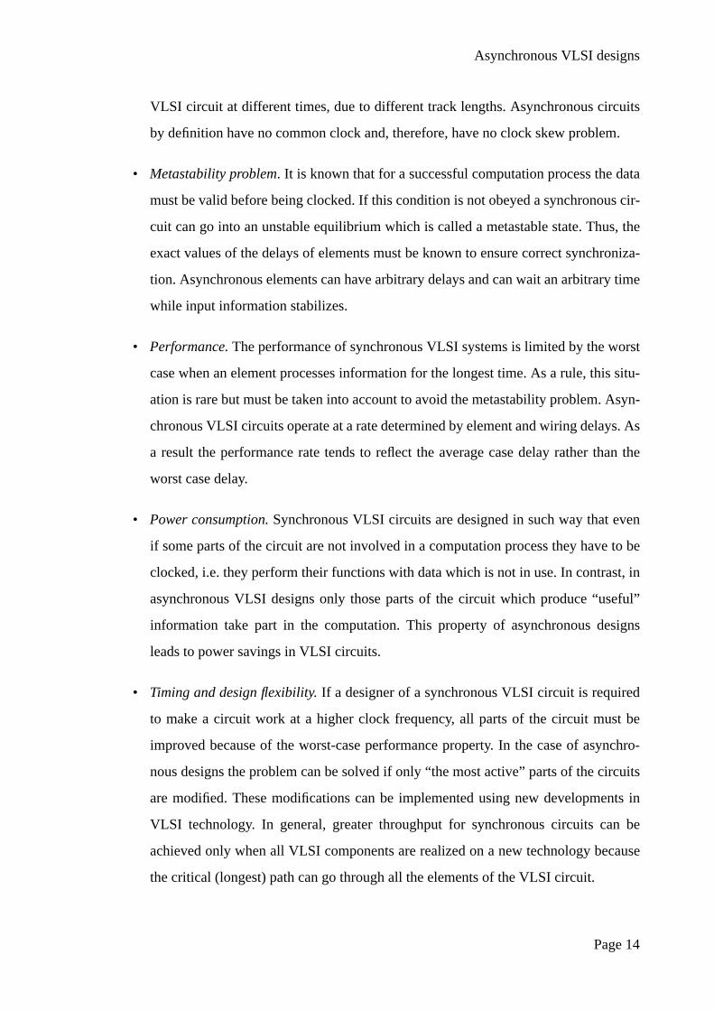
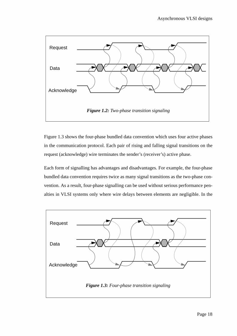
Figure 1.3 shows the four-phase bundled data convention which uses four active phases
in the communication protocol. Each pair of rising and falling signal transitions on the
request (acknowledge) wire terminates the sender’s (receiver’s) active phase.
Each form of signalling has advantages and disadvantages. For example, the four-phase
bundled data convention requires twice as many signal transitions as the two-phase con-
vention. As a result, four-phase signalling can be used without serious performance pen-
alties in VLSI systems only where wire delays between elements are negligible. In the
Request
Data
Acknowledge
Figure 1.2: Two-phase transition signaling
Request
Data
Acknowledge
Figure 1.3: Four-phase transition signaling

Asynchronous VLSI designs
Page 19
two-phase bundled data convention the interpretation of transitions requires more con-
trol logic than four-phase signalling requires.
1.4 Event-controlled logic elements
Asynchronous circuits which use transition signalling protocols for controlling data flow
require basic control building blocks which differ from synchronous ones. All event-
controlled logic elements are bistable digital circuits which form various logical combi-
nations of events. Figure 1.4 shows an assembly of the most frequently used asynchro-
nous logic modules for events [3].
The simplest module is theExclusive-OR (XOR) element which has a function equiva-
lent to merging two events: if an event is received on either of the inputs of an XOR ele-
ment a response event will be produced on the output of the element.
TheMuller C-element performs a logical AND of input events. When all the inputs of
a Muller C-element are ones (zeros) the Muller C-element generates an one (zero) on its
output and stores this state. If the inputs are different the Muller C-element retains its
previous state and holds the output unchanged. Therefore, the Muller C-element pro-
duces an event when an event takes place on each its input. Because of this property the
Muller C-element is sometimes called a “rendezvous” circuit.
The Toggle circuit sends a transition alternately to one or other of its outputs when an
event appears on its input. The first event is generated on the dotted output.
TheSelect module is a demultiplexer of two events. It steers a transition to one of two
outputs depending on the logical value on its diamond input.
TheCall element serves a function which is similar to a subroutine call in programming.
It remembers which one of its two inputs received an event first,r1 or r2, and calls the
procedure,r. After the procedure is finished,d, the Call element produces a matching
done event ond1 or d2 output.

Asynchronous VLSI designs
Page 20
The Arbiter guarantees that both of its outputs are not active at the same time. The arbi-
tration function is in granting service, g1 or g2, to only one request, r1 or r2, at a time.
The other grant is delayed until after an event has taken place on the done wire, d1 or
d2, corresponding to the earlier grant.
1.5 Asynchronous micropipelines
A pipeline is a mechanism used for speeding up the throughput in a computer system.
The main reason for using pipelines is to increase the number of elements doing compu-
tations at a given time. A micropipeline is a data processing pipeline whose stages oper-
ate asynchronously. There are several papers which describe basic principles for
designing asynchronous micropipelines [3, 5]. Figure 1.5 represents the general struc-
C
TOGGLE
SELECTtrue false
r1
d1
d2
r2
r
dCA
LL
g1
d1
g2d2
r1
r2 AR
BIT
ER
Exclusive-OR
Muller C-element
TOGGLE element
SELECT module
ARBITER
CALL element
Figure 1.4: An assembly of basic logic modules for events
Asynchronous VLSI designs
Page 21
ture of a two-phase micropipeline incorporating computation. The registers in the pic-
ture are similar to level sensitive latches which are usually used in synchronous designs.
The only difference is that they respond to transitions on two inputs instead of a single
clock wire. Initially all registers pass data directly from their inputs to outputs. When a
transition takes place on the C (capture) control input the current binary vector is latched
in the register. Once a transition occurs on the P (pass) wire the register returns to a
transparent state and the computation cycle repeats. The register output Cd (Pd) is the
capture-done (pass-done) output on which a delayed version of the capture (pass) event
is generated. If a transition is stored in the FIFO control logic the data will be buffered in
the registers. Since each computation logic block has its internal delay the Cd signal
transition must be delayed by as much as the worst-case logic block delay. Without the
logic blocks the micropipeline (Figure 1.5) is a FIFO buffer.
Using the same approach to designing micropipelines an asynchronous sequential cir-
cuit can easily be produced. Figure 1.6 shows the basic structure of such a circuit. This
structure uses two registers, RG1 and RG2; register RG1 holds the previous state of the
circuit and the new state is stored into register RG2. In the initial state the initial binary
vector is written into RG1. As a result a high voltage level is generated on the Cd output
of RG1, Pd output of RG2 and the acknowledge output of the circuit, A(in). The
delay
delay
delay
delay
CCd P
PdC
Cd
P
Pd
CCd
P
Pd
C
Cd P
Pd
C
CC
C
LOG
IC
LOG
IC
LOG
IC
LOG
IC
RG RG RG RG
R(in) R(out)
A(out)A(in)
Data Data
Figure 1.5: A computation micropipeline

Asynchronous VLSI designs
Page 22
request event is produced by the sender when the primary inputs,PI, are stable. The
request signal is delayed for sufficient time to ensure stable levels on the internal and
primary outputs,PO, of the logic block. After storing the new state of the sequential cir-
cuit into RG2 the request event for the receiver is formed on theCd output ofRG2.
After the acknowledge event on theA(out) wire takes place the new state is copied from
RG2 to RG1 and the circuit produces the acknowledge signal transition for the sender.
Thus, after a new request event from the sender is registered the computation cycle of
the sequential circuit is repeated.
A major advantage of the micropipeline structure is the possibility of filtering out all
hazards in the logic blocks. Another positive feature is that an asynchronous micropipe-
line is automatically elastic; that is, data can be sent to and received from a micropipe-
line at arbitrary times. Although micropipelines are a powerful tool for implementing
elastic pipelines they have one serious drawback. The micropipeline approach is inher-
ently bounded-delay rather than delay-insensitive. In order to yield a completely delay-
insensitive system the timing information must be encoded with the data itself.
C
CC
PPd
C Cd
PPd
C Cd
RG1 RG2
delay
LOGIC
A(in)
R(in) R(out)
A(out)
Figure 1.6: An asynchronous sequential circuit
PI PO

Asynchronous VLSI designs
Page 23
1.6 Summary
Asynchronous VLSI circuits are becoming a serious alternative to synchronous circuits
because of the absence of global clock distribution. One of the most attractive models to
implement asynchronous circuits is the bounded-delay model. Specifically, it is assumed
that the delay in all circuit elements and wires is known, or at least bounded. Such asyn-
chronous circuits can be designed easily using fundamental principles for designing syn-
chronous hardware and a pipelined approach. Unfortunately, bounded-delay
asynchronous circuits are complex systems where multiple control state machines and
data path elements are combined to implement the desired function. This leads to spe-
cific difficulties in solving the fault detection problem, which is the subject for discus-
sion in the following chapters.

Page 24
Chapter 2 : Testing VLSI circuits
2.1 Problems in testing VLSI circuits
The ability to put millions of transistors on a single chip of silicon creates great potential
for reducing power, increasing speed, and drastically reducing the cost of VLSI circuits.
Unfortunately, several serious problems must be solved in order to exploit these advan-
tages. The main problem is that of identifying faulty and fault-free VLSI designs before
and after fabrication. A large number of CAD tools has been developed to help design
engineers do logic and design verification [1, 2, 8, 9]. Several test generation algorithms
have been devised to detect faulty VLSI circuits after their physical implementation [9-
14]. The major problems which make the testing of either synchronous or asynchronous
VLSI circuits difficult or even impossible are:
• Test generation and testing time and consequently testing costs are increasing rapidly
with increasing VLSI circuit complexity. The increasing complexity of VLSI circuits
causes the controllability of the inputs and the observability of the outputs of VLSI
elements to be more and more problematic. At the same time the sequential depth of
VLSI circuits is increasing. It has been shown that the cost for test generation
increases as an exponential function of the sequential depth of the network [11].
• In order to test VLSI circuits test engineers have to deal with enormous amounts of
diagnostic information which demands the use of complex and expensive test equip-
ment.
• Rapid changes in VLSI technology create the possibility of physical defects mani-
festing themselves in a large number of ways. In some cases traditional fault models
for such circuits cannot be used to determine the fault coverage of test patterns.
Testing VLSI circuits
Page 25
• The Application Specific Integrated Circuit (ASIC) market requires design engineers
to produce VLSI circuits as quickly as possible, reducing the time for estimating the
testability of new products. The low production volumes of ASICs makes test costs a
significant part of the overall costs.
2.2 Fault models for VLSI circuits
A VLSI circuit failure occurs when the circuit produces output information which devi-
ates from the result which is defined by the specification. The failure occurs because the
VLSI circuit is erroneous, i.e. there is an error in part of the circuit which leads to fail-
ure. The cause of the error is a fault. Thus, an error is the manifestation of a fault in the
VLSI circuit, and a failure is the effect of an error. In VLSI circuits all faults can be
divided into two classes [9]: physical faults and human-made faults, which may be
defined as follows:
• physical faults: adverse physical phenomena, either internal (physico-chemical disor-
ders: threshold changes, short circuits, open circuits, etc.) or external (changes in
environmental conditions: electromagnetic perturbations, temperature, vibrations,
etc.);
• human-made faults: imperfections which are design faults or interaction faults caused
by violations of operating or maintenance procedures.
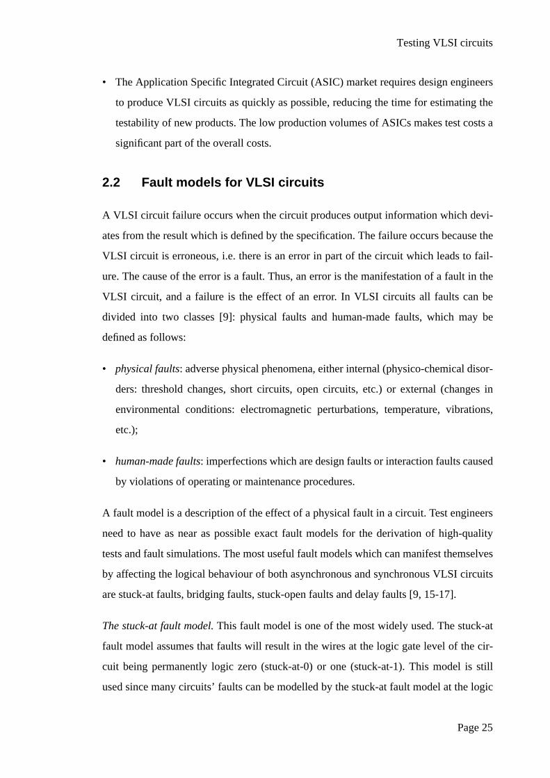
A fault model is a description of the effect of a physical fault in a circuit. Test engineers
need to have as near as possible exact fault models for the derivation of high-quality
tests and fault simulations. The most useful fault models which can manifest themselves
by affecting the logical behaviour of both asynchronous and synchronous VLSI circuits
are stuck-at faults, bridging faults, stuck-open faults and delay faults [9, 15-17].
The stuck-at fault model. This fault model is one of the most widely used. The stuck-at
fault model assumes that faults will result in the wires at the logic gate level of the cir-
cuit being permanently logic zero (stuck-at-0) or one (stuck-at-1). This model is still
used since many circuits’ faults can be modelled by the stuck-at fault model at the logic

Testing VLSI circuits
Page 26
level. Theoretically, for any circuit the total number of all possible faulty circuits with
multiple stuck-at faults can be estimated as , where is the number of nodes in
the circuit. In practice, only single stuck faults are considered in order to eliminate an
incredibly large number of faulty VLSI circuits.
Figure 2.1 shows an NMOS NOR gate with four faults: faults 1 and 2 being shorts
(shown as dotted lines) and faults 3 and 4 being opens (depicted by crosses). Table 2.1
gives the behaviour of the gate when all possible two-bit binary vectors are applied
under these four faults. Outputs are shown for no fault ( ), for the two shorts ( and
) and for the two opens ( and ). Fault 1 is logically equivalent to the A input
stuck-at-0 since the gate cannot be driven to logic 0 when A=1 and B=0. Fault 4 is
equivalent to the B input stuck-at-1 and can be detected by applying A=0, B=1. If the
Table 2.1: The truth table of NMOS NOR gate with four faults
Inputs Outputs
0 0 1 1 1 1
0 1 0 0 u 0 1
1 0 0 1 0 0 0
1 1 0 0 0 0 0
3n 1− n
A B
F
VDD
1
2
3
4
AB
F
Figure 2.1: NMOS NOR gate with four faults
F0 F1
F2 F3 F4
A B F0 F1 F2 F3 F4
Qn
Testing VLSI circuits
Page 27
short marked 2 is present, then under the input 01, the output may not be 0 but may be an
indeterminate voltage represented asu. Thus, under this fault and this input combina-
tion, the output is permanently stuck at 0 or 1. This example demonstrates that in some
cases the stuck-at fault model cannot be accurate.
The bridging fault model. Bridging faults are the result of many physical faults which at
the circuit level will produce shorts between interconnecting lines. In TTL technology
this model treats shorts between lines in the logic gate network and assumes that all
affected lines will have the wired-AND or wired-OR logic value under fault [15]. It has
been shown that the bridging fault can convert a combinational circuit to a sequential
one in CMOS technology [14]. This, in turn, creates extra problems in the testing of
VLSI circuits.
The stuck-open fault models. These kinds of faults are inherent to MOS technology [16].
In the case of a stuck-open fault an open transistor (or a broken line) can lead to a MOS
gate behaving as if it had memory. For example, fault 3 in the NMOS NOR gate (Figure
2.1) produces a high-impedance output under the combination 00 (Table 2.1). In NMOS
technology this means that the gate stores the previous output (shown as) at least for
a period of time until any residual charge leaks away from the output. Fault 3 can mani-
fest itself on the output of the gate only under a certain sequence of input combinations.
If two input vectors are applied as 11, 00, then the fault will be detected since will be
a 0 and the correct output should be a 1. If the 00 combination was applied first, when
the output wire was 1, fault 3 would not be detected.
Delay faults. A delay fault is a fault on an element or path that alters its delay. In syn-
chronous VLSI circuit such a fault would require the chip to be clocked at a slower rate.
However, in an asynchronous VLSI circuit there is no clock to slow down, and a delay
fault can cause incorrect circuit operation that in some particular cases cannot be fixed.
For instance, in Figure 2.2, a pulse generator drives a pulse detector. The delay in the
pulse detector feedback line is designed to be smaller than the pulse generator’s pulse
width. As a result, the pulse detector remains 1 after the first pulse is detected. If a delay
fault occurs in the pulse detector delay, the feedback value may not arrive before the
Qn
Qn

Testing VLSI circuits
Page 28
pulse has ended. Thus, the pulse detector will oscillate. Methods for detecting delay
faults have been developed [17, 18]. Unfortunately, they require complex test equipment
capable of applying multiple test sequences rapidly and checking data at specific times.
Although the stuck-at fault model is widely accepted by test engineers as a standard for
measuring test coverage, this model is now becoming inadequate as new failure mecha-
nisms are being discovered for VLSI circuits.
2.3 Logic testing of VLSI circuits
All test procedures assume the application of a set of patterns (“tests”) to the inputs of
the circuit under test (CUT) and an analysis of the responses obtained. If the CUT pro-
duces the right outputs it means that it is fault free for the predefined class of faults.
Most test methods separate the testing process from normal operation in order to provide
a higher degree of fault coverage [13, 19, 20]. Basically, a test procedure includes three
main steps: test pattern generation, applying the set of test patterns to the CUT, and eval-
uating the responses observed on the outputs of the CUT (Figure 2.3). The aim of the
test pattern generation step is to derive those tests which will detect all possible faults
from the set of faults. The test patterns can be applied in two ways. The first way is to
use external test equipment to apply tests to the CUT and check the responses. The sec-
ond way presumes the application of test patterns inside the CUT. The method of apply-
ing test patterns internally is suitable for realization in VLSI systems for arranging self-
testing procedures [21]. The results of the process of evaluating the responses obtained
PulseGenerator Pulse
Detector
Figure 2.2: Delay fault hazard in an asynchronous VLSI circuit

Testing VLSI circuits
Page 29
from the CUT can help to solve two test tasks: the definition of a faulty circuit (so called
go/no-go testing) and, in addition to this, the indication of the position of the fault in the
CUT (fault location testing) [20]. Go/no-go testing is reasonable for testing VLSI chips
as a chip is a replaceable element in most VLSI systems. Both test methods can be used
for testing VLSI systems.
2.3.1 Test generation methods
The main goal for the test generation process is to derive those input patterns which,
when applied to the CUT, will sensitize any existing faults (the controllability problem)
and propagate an incorrect response to the observable outputs of the CUT (the observa-
bility problem) [10]. A test set is good if it is capable of detecting a high percentage of
faults from the possible CUT faults or simply if it can guarantee a high fault coverage.
Before designing tests for a digital circuit a test engineer has to solve two problems: to
Goo
d re
spon
se g
ener
atio
n
Test generation Test application Response evaluation
VLSI logic testing
Ran
dom
/ P
seud
o-ra
ndom
Ext
erna
l
Inte
rnal
Com
pact
test
ing
Figure 2.3: VLSI logic testing
Exh
aust
ive
Alg
orith
mic
Testing VLSI circuits
Page 30
chose an appropriate descriptive model for the CUT (the description at the transistor,
gate or register transfer level) and to develop a fault model to define the result of a phys-
ical fault. Obviously, the lower the level of circuit representation used in test pattern
generation, the more accurate the fault model will be. However, the use of low level
description languages for VLSI circuits having many thousands of transistors aggravates
the problem of test pattern generation drastically. It has been shown that the problem of
generating a test set for single stuck-at faults in a combinational circuit represented at
the gate level is an NP-complete problem [22]. For a sequential circuit the test genera-
tion problem becomes much more difficult since the number of incorporated memory
elements increases. Thus, in each particular case a test engineer must find a compromise
between the time to derive the test and the level of fault coverage achieved by the test.
Basically, approaches to test generation can be divided into three groups: exhaustive
testing, random (pseudo-random) testing and algorithmic test generation methods (Fig-
ure 2.3). Exhaustive testing assumes the application of all possible input vectors to the
CUT. If a faulty combinational circuit has a fault which does not result in sequential cir-
cuit behaviour the application of all possible binary vectors to the inputs of the CUT can
guarantee 100% fault coverage. For the exhaustive testing of a circuit with a large
number of inputs the number of tests becomes incredibly large. An approach to extend-
ing the exhaustive test technique to large circuits by means of partitioning the CUT into
subcircuits any of which can be tested for a reasonable time has been described [23].
However, this approach has a major problem concerned with finding the most suitable
partitions.
In random (pseudo-random) testing [14, 24, 25], input vectors are produced with the
help of random (pseudo-random) test pattern generators. The reactions of the faulty and
the fault-free circuits for each random vector are compared using a simulator. If the
responses are different the current vector is put into a test set. The main advantage of all
random (pseudo random) generation techniques is that the test engineer has a source of
test patterns and only the problem to be solved is that of proving that the random test set
has the desired fault coverage.
Testing VLSI circuits
Page 31
Many algorithms have been proposed [9-14] for generating test vectors for either combi-
national or sequential circuits. The majority of these methods generate test sequences by
means of analysing the topological structure of the CUT. Such well-known path sensiti-
zation algorithms as the D-algorithm [10], PODEM [14] and FAN [9] have successfully
been used for automatic test generation for VLSI circuits.
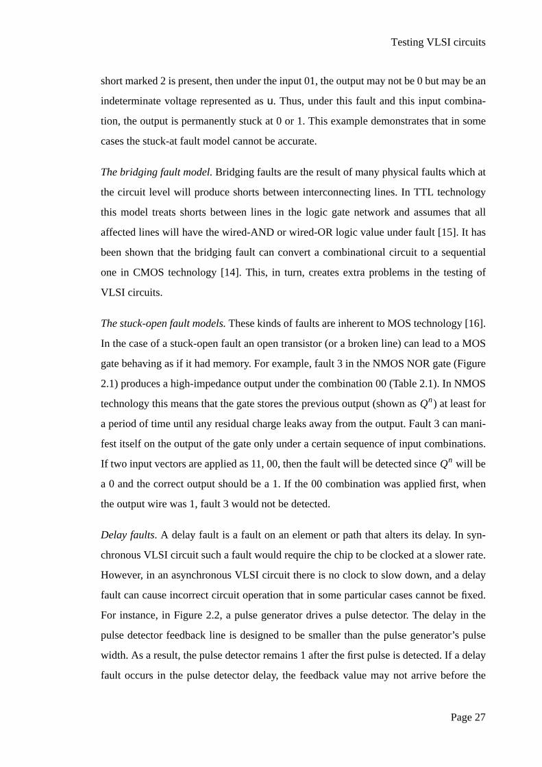
The concept of the path sensitization technique is illustrated in Figure 2.4. The deriva-
tion procedure for the stuck-at fault on lined includes three sequential steps marked by
circled numbers. The goal of the first step is to set lined to 0. In Figure 2.4 the logical
value before the slash is the correct value for the fault-free circuit; the value after the
slash is the logical result in the faulty circuit. On the second step, linea should be set to
0 in order to justify the previous step. The last test generation step makes the effect of
the fault on lined propagate to the outpute by setting lineb to 0. As a result, test pattern
00 can be applied to detect the stuck-at-1 fault on lined.
As shown above, the main point of path sensitization algorithms is in analysing the cir-
cuit topology in order to construct an input vector which will sensitize a path from the
fault site to a primary output. The process of path sensitization consists of three basic
operations: justification, implication and propagation [13]. Step 2 of the above example
is justification for generating a logical 0 on noded. In general, when a value is assigned
to a certain node, it may imply other logical values for some lines of the circuit. The aim
of the implication procedure is to cause forward propagation of the result of the justifica-
tion step. For example, a logical 0 can be set on lined by setting a logical 1 on lineb
(see Figure 2.4). In this case the effect of the fault on lined cannot be propagated
a
b
cd
e
1
2
3
Stuck-at-1
0
0/1
1/0
0
Figure 2.4: Path sensitization technique
1

Testing VLSI circuits
Page 32
through the NOR gate to the outpute. Therefore, the result of the justification step can
be propagated only if a logical 0 is set on linea. The effect of the propagation process
(step 3) is to move the fault effect through a sensitized path to an output of the circuit.
One of the classical methods for detecting stuck-at faults is the D-algorithm [10] which
employs the path sensitization technique. The set of five elements {0, 1,, , } for
representing signals is used to facilitate the path sensitization process. means
unknown. represents a signal which has the value 1 in a normal circuit and 0 in a
faulty circuit. is the complement of . The D-algorithm consists of three parts: fault
excitation and forward implication, D-propagation, backward justification. On the first
step the minimal input conditions are selected in order to produce an error signal ( or
) on the output (faulty node) of the logic element. The forward implication process is
performed in order to determine the outputs of those gates whose inputs are specified.
The goal of the D-propagation step is to propagate the fault effect to primary outputs by
means of assigning logical values to corresponding internal lines and primary inputs. In
backward justification, node values are justified from primary inputs. If there is a con-
flict in one of the nodes the backwards consideration from the conflict node to the pri-
mary inputs is reiterated until the fault effect ( or ) reaches at least one of the
primary outputs.
Not all the stuck-at faults of the CUT can be detected by path sensitization algorithms.
Hardware redundancy is the reason why these faults cannot be detected. For example,
the stuck-at-1 fault on nodec of the circuit shown in Figure 2.4 is undetectable since
there is no sensitization path from the fault site to the output of the CUT. It is easy to
ensure that while the stuck-at-1 fault is present on nodec the faulty circuit produces the
correct responses. Clearly, the combinational circuit shown in Figure 2.4 produces the
following Boolean function: . This function is redundant and equivalent to
which is not redundant.
Although path sensitization techniques formalize the test derivation procedure, they can
no longer be used in testing VLSI circuits due to drastically increasing test generation
time.
X D D
X
D
D D
D
D
D D
a b b+⋅
a b+
Testing VLSI circuits
Page 33
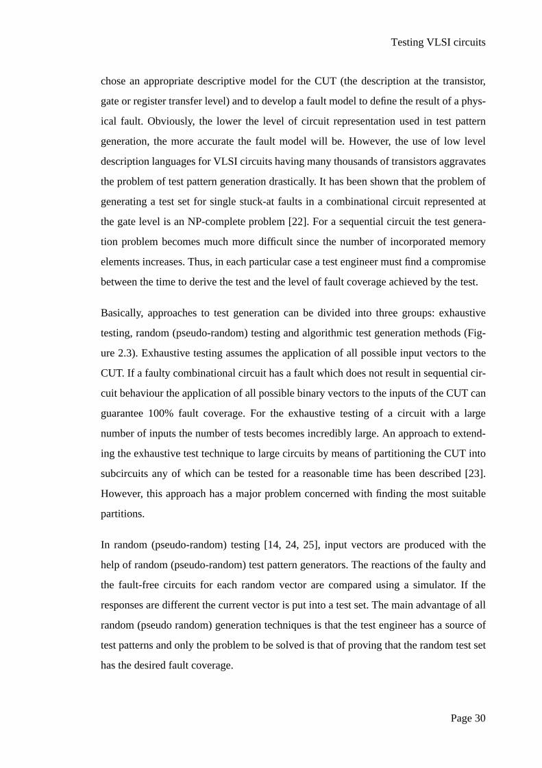
2.3.2 Response evaluation techniques
The main goal for response evaluation is to detect any wrong response. There are two
basic approaches for achieving this goal. The first approach uses a good response gener-
ator and the second one is based on principles of compact testing techniques.
In good response generation techniques the major problem is to choose a method of
obtaining a good response for the CUT. Any faulty response can be detected by compar-
ing good responses with responses produced on the outputs of the CUT. In the stored
response testing technique (Figure 2.5) all good responses are stored in a ROM. After
applying each test pattern to the CUT the actual response is compared with the good
one. If they are different the comparator will activate an error signal at its output. Good
responses can easily be obtained by means of software-simulation of the VLSI circuit as
a part of the design verification stage [9].
Figure 2.6 shows the flow diagram for the comparison testing technique. In order to
detect any faulty response test patterns are applied to the inputs of the CUT and a golden
unit simultaneously and the responses of both units are compared by the comparator.
In comparison with stored response testing, comparison testing has some advantages:
1) it allows the testing of VLSI circuits over a large range of speeds and electrical
parameters because the golden unit and the CUT are operated under the same condi-
tions;
Test patterns CUT CUT response
Stored goodresponse
Comparator
Figure 2.5: Stored response testing
Error
Testing VLSI circuits
Page 34
2) a change in the test sequence does not require any change in the test process.
On the other hand, the stored response testing technique needs to store good responses
(the results of simulation) only once before testing whereas the quality of comparison
testing depends on the quality of the golden unit.
The main drawback of the response evaluation techniques is the necessity to operate
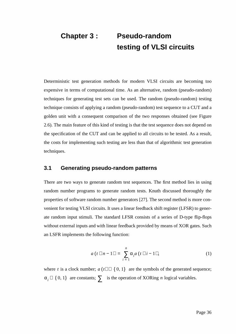
with a large amount of response data during the testing of VLSI circuits. In order to sim-
plify the problem of storing and analysing test responses the compact testing methods
have been devised [14]. The general idea of compact testing is to compress the response
data into a compact form during the test. After the test is complete the response of the
CUT is compared with the compressed response of the golden unit. A basic diagram of
the compact testing technique is shown in Figure 2.7. However, during the compression
process there is a probability that some part of the diagnostic information from the
Test patterns
CUT CUT response
Goodresponse
Comparator
Golden unit
Error
Figure 2.6: Comparison testing
Test patterns
CUT
Comparator
Figure 2.7: Compact testing
Error
compressedresponse
Good
CompressionfunctionResponses

Testing VLSI circuits
Page 35
response data flow will be lost. This in turn creates the possibility of making a wrong
decision about the test results. All the compact testing methods differ in the method of
data compression. The most widely used compact testing methods are transition count-
ing [14] and signature analysis [19, 26]. The transition counting method compresses the
response data into the number of 0 to 1 and 1 to 0 transitions in the sequence. In the sig-
nature analysis technique the response data are compressed using a signature analyser
built as a linear feedback shift register. This method will be described in more detail in
Chapter 3.
Page 36
Chapter 3 : Pseudo-random
testing of VLSI circuits
Deterministic test generation methods for modern VLSI circuits are becoming too
expensive in terms of computational time. As an alternative, random (pseudo-random)
techniques for generating test sets can be used. The random (pseudo-random) testing
technique consists of applying a random (pseudo-random) test sequence to a CUT and a
golden unit with a consequent comparison of the two responses obtained (see Figure
2.6). The main feature of this kind of testing is that the test sequence does not depend on
the specification of the CUT and can be applied to all circuits to be tested. As a result,
the costs for implementing such testing are less than that of algorithmic test generation
techniques.
3.1 Generating pseudo-random patterns
There are two ways to generate random test sequences. The first method lies in using
random number programs to generate random tests. Knuth discussed thoroughly the
properties of software random number generators [27]. The second method is more con-
venient for testing VLSI circuits. It uses a linear feedback shift register (LFSR) to gener-
ate random input stimuli. The standard LFSR consists of a series of D-type flip-flops
without external inputs and with linear feedback provided by means of XOR gates. Such
an LSFR implements the following function:
, (1)
where is a clock number; are the symbols of the generated sequence;
are constants; is the operation of XORing logical variables.
a t n 1−+( ) αia t i 1−+( )i 1=
n
∑=
t a t( ) 0 1,{ }∈
αi 0 1,{ }∈ ∑ n

Pseudo-random testing of VLSI circuits
Page 37
Figure 3.1 shows the general structure of an LFSR. Symbol indicates the presence
( ) or absence ( ) of a feedback connection from the output of theth stage
to the XOR network. Sometimes the coefficients are called “taps” since they deter-
mine the structure of the LFSR.
An LFSR can be realized in a modular form depicted in Figure 3.2. The modular realiza-
tion of an LFSR [28] has the same number of XOR gates as the standard structure,
which is defined by feedback taps. If the number of feedback signals,, is more than 2,
the modular LFSR is faster than the standard one: the former has one gate propagation
delay whereas the standard LFSR has gate delays per one clock.
If a homogeneous Bernouilli process [29] is used for simulating the behaviour of an
LFSR such a procedure is called “random pattern generation”. As the nature of the pat-
XOR
n-1 n-2 1 0
αnαn 1− α3 α2 α1
a(t+n-1) a(t+n-2) a(t+2) a(t+1) a(t)
Figure 3.1: Linear feedback shift register
αi
αi 1= αi 0= i
αi
n-1 n-2 1 0
αnαn 1−α3α2α1
bn t( ) bn 1− t( ) b2 t( ) b1 t( )
Figure 3.2: Modular realization of a LFSR
k
k 1−
Pseudo-random testing of VLSI circuits
Page 38
terns generated by an LFSR is deterministic, a non-homogeneous Bernouilli process can
be used for simulation. This is called pseudo-random pattern generation [24].
It is easy to show that for a certain combination of coefficients the period of the
sequence, , generated by an LFSR will be maximal and equal to .
Although such a sequence can be characterized by equiprobable and randomly appear-
ing 1s and 0s, as in a truly random sequence [30], the signals generated by an LFSR can
be reproduced repeatedly after setting it into the initial state. For this reason, the
sequences produced by maximal-length LFSRs are called pseudo-random sequences to
distinguish them from truly random sequences. Pseudo-random sequences are more
suitable for testing digital circuits than truly random ones due to the possibility of
repeating them for simulation purposes.
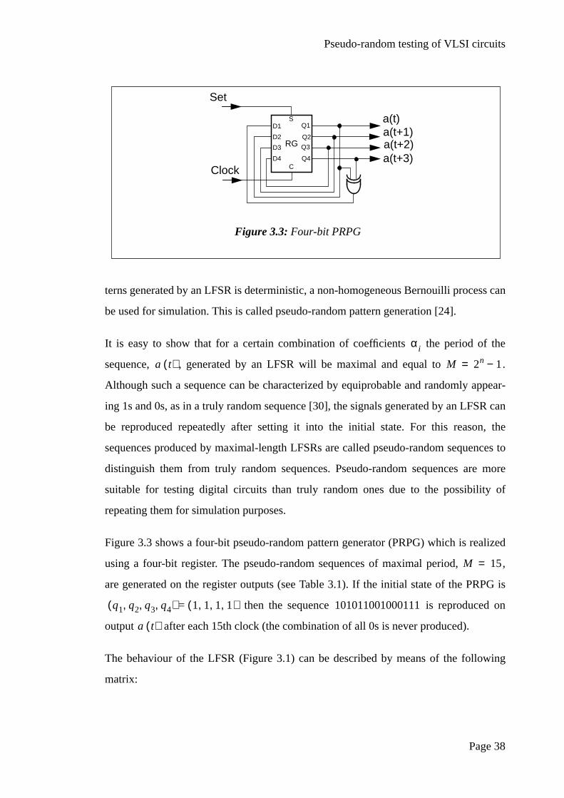
Figure 3.3 shows a four-bit pseudo-random pattern generator (PRPG) which is realized
using a four-bit register. The pseudo-random sequences of maximal period, ,
are generated on the register outputs (see Table 3.1). If the initial state of the PRPG is
= then the sequence is reproduced on
output after each 15th clock (the combination of all 0s is never produced).
The behaviour of the LFSR (Figure 3.1) can be described by means of the following
matrix:
αi
a t( ) M 2n 1−=
M 15=
q1 q2 q3 q4, , ,( ) 1 1 1 1, , ,( ) 101011001000111
a t( )
RG
D1
D2
D3
D4
Q2
Q3
Q4
Q1
C
S
Clock
Set
a(t)a(t+1)a(t+2)a(t+3)
Figure 3.3: Four-bit PRPG

Pseudo-random testing of VLSI circuits
Page 39
, (2)
where the values of all the coefficients are defined by the feedback connections of the
LFSR. The elements of the first row determine the XOR operation. The other elements
of matrix (2) define the shift operation. If the sequence of LFSR states is denoted by=
then the operational sequence can be represented as
(3)
Equation (3) can be rewritten in a short form as . It is necessary
to mention that time is discrete. Multiplying the current state by matrix
Table 3.1: State sequence for the four-bit PRPG
State State
0 1 1 1 1 8 1 0 0 1
1 0 1 1 1 9 0 1 0 0
2 1 0 1 1 10 0 0 1 0
3 0 1 0 1 11 0 0 0 1
4 1 0 1 0 12 1 0 0 0
5 1 1 0 1 13 1 1 0 0
6 0 1 1 0 14 1 1 1 0
7 0 0 1 1 15 1 1 1 1
Q1 Q2 Q3 Q4 Q1 Q2 Q3 Q4
A
α1 α2
1 0
0
…0
1
…0
… αn 1− αn
… 0 0
…
……
0
…1
0
…0
=
αi
Q
q1 q2 … qn, , ,( )
q1 t( )q2 t( )
…qn 1− t( )
qn t( )
α1 α2
1 0
0
…0
1
…0
… αn 1− αn
… 0 0
…
……
0
…1
0
…0
q1 t 1−( )q2 t 1−( )
…qn 1− t 1−( )
qn t 1−( )
=
Q t( ) A Q t 1−( )⋅=
t Q t( ) A s
Pseudo-random testing of VLSI circuits
Page 40
times, the LFSR state at time ( ) can be found, i.e. . The
number is called the period of LFSR if or , where
is the identity matrix.
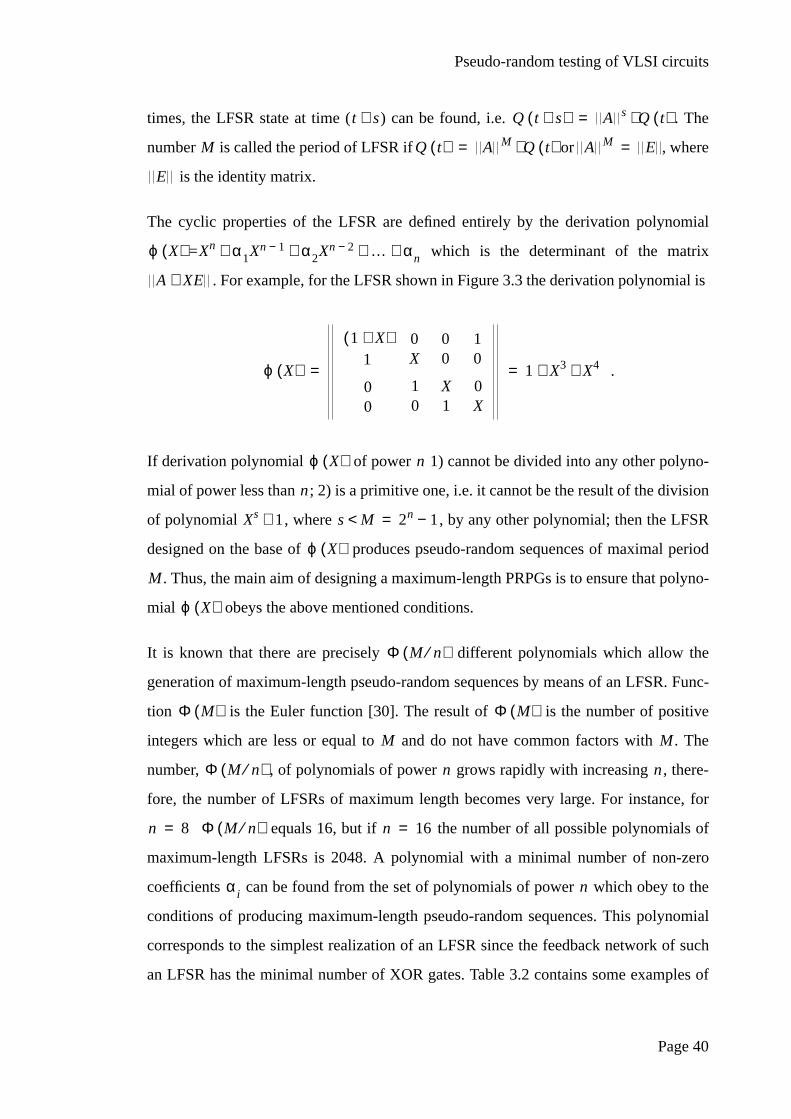
The cyclic properties of the LFSR are defined entirely by the derivation polynomial
= which is the determinant of the matrix
. For example, for the LFSR shown in Figure 3.3 the derivation polynomial is
.
If derivation polynomial of power 1) cannot be divided into any other polyno-
mial of power less than; 2) is a primitive one, i.e. it cannot be the result of the division
of polynomial , where , by any other polynomial; then the LFSR
designed on the base of produces pseudo-random sequences of maximal period
. Thus, the main aim of designing a maximum-length PRPGs is to ensure that polyno-
mial obeys the above mentioned conditions.
It is known that there are precisely different polynomials which allow the
generation of maximum-length pseudo-random sequences by means of an LFSR. Func-
tion is the Euler function [30]. The result of is the number of positive
integers which are less or equal to and do not have common factors with. The
number, , of polynomials of power grows rapidly with increasing, there-
fore, the number of LFSRs of maximum length becomes very large. For instance, for
equals 16, but if the number of all possible polynomials of
maximum-length LFSRs is 2048. A polynomial with a minimal number of non-zero
coefficients can be found from the set of polynomials of power which obey to the
conditions of producing maximum-length pseudo-random sequences. This polynomial
corresponds to the simplest realization of an LFSR since the feedback network of such
an LFSR has the minimal number of XOR gates. Table 3.2 contains some examples of
t s+ Q t s+( ) A s Q t( )⋅=
M Q t( ) A M Q t( )⋅= A M E=
E
ϕ X( ) Xn α1Xn 1− α2Xn 2− … αn+ + + +
A XE+
ϕ X( )
1 X+( )1
00
0X
10
00
X1
10
0X
1 X3 X4+ += =
ϕ X( ) n
n
Xs 1+ s M< 2n 1−=
ϕ X( )
M
ϕ X( )
Φ M n⁄( )
Φ M( ) Φ M( )
M M
Φ M n⁄( ) n n
n 8= Φ M n⁄( ) n 16=
αi n
Pseudo-random testing of VLSI circuits
Page 41
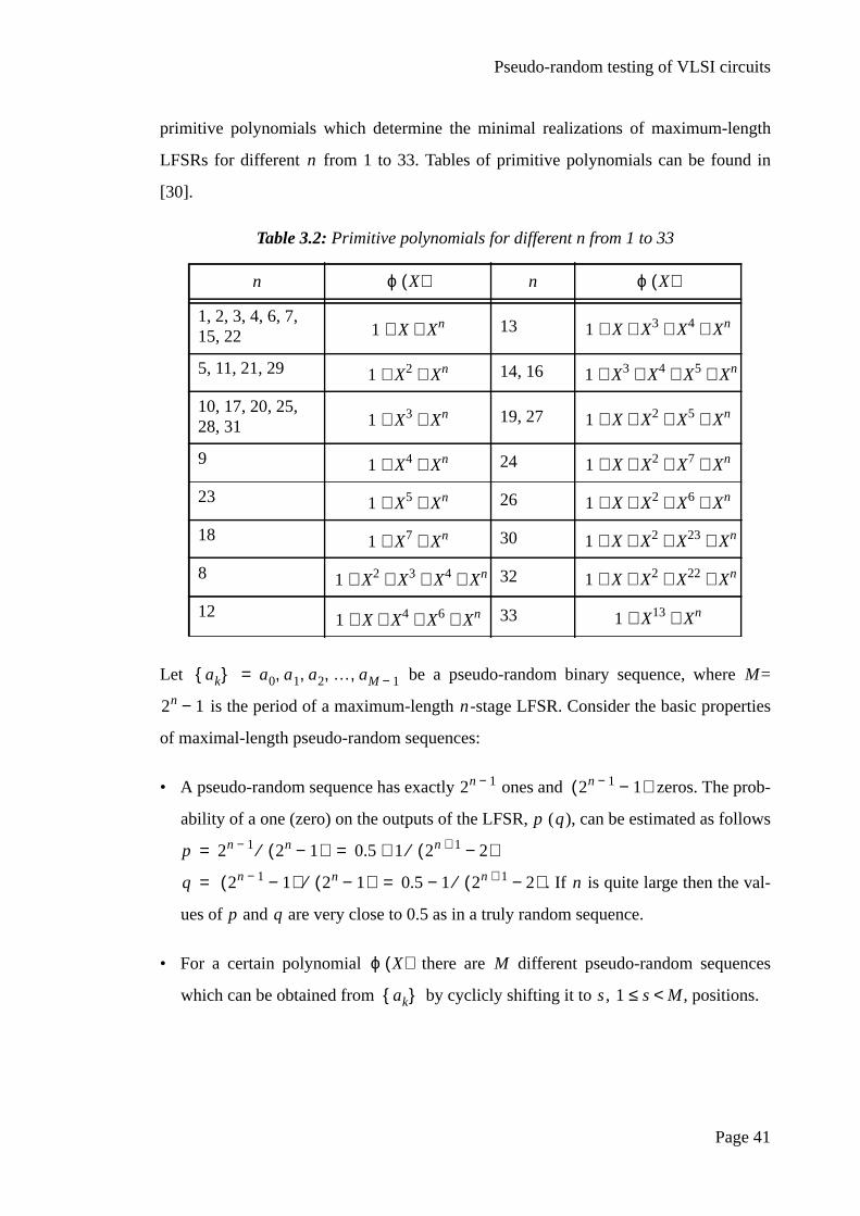
primitive polynomials which determine the minimal realizations of maximum-length
LFSRs for different from 1 to 33. Tables of primitive polynomials can be found in
[30].
Let be a pseudo-random binary sequence, where=
is the period of a maximum-length-stage LFSR. Consider the basic properties
of maximal-length pseudo-random sequences:
• A pseudo-random sequence has exactly ones and zeros. The prob-
ability of a one (zero) on the outputs of the LFSR, ( ), can be estimated as follows
. If is quite large then the val-
ues of and are very close to 0.5 as in a truly random sequence.
• For a certain polynomial there are different pseudo-random sequences
which can be obtained from by cyclicly shifting it to , , positions.
Table 3.2: Primitive polynomials for different n from 1 to 33
1, 2, 3, 4, 6, 7,15, 22
13
5, 11, 21, 29 14, 16
10, 17, 20, 25,28, 31
19, 27
9 24
23 26
18 30
8 32
12 33
n
n ϕ X( ) n ϕ X( )
1 X Xn+ + 1 X X3 X4 Xn+ + + +
1 X2 Xn+ + 1 X3 X4 X5 Xn+ + + +
1 X3 Xn+ + 1 X X2 X5 Xn+ + + +
1 X4 Xn+ + 1 X X2 X7 Xn+ + + +
1 X5 Xn+ + 1 X X2 X6 Xn+ + + +
1 X7 Xn+ + 1 X X2 X23 Xn+ + + +
1 X2 X3 X4 Xn+ + + + 1 X X2 X22 Xn+ + + +
1 X X4 X6 Xn+ + + + 1 X13 Xn+ +
ak{ } a0 a1 a2 … aM 1−, , , ,= M
2n 1− n
2n 1− 2n 1− 1−( )
p q
p 2n 1− 2n 1−( )⁄ 0.5 1 2n 1+ 2−( )⁄+= =
q 2n 1− 1−( ) 2n 1−( )⁄ 0.5 1 2n 1+ 2−( )⁄−= = n
p q
ϕ X( ) M
ak{ } s 1 s M<≤

Pseudo-random testing of VLSI circuits
Page 42
• In sequence there is only one combination of 1s and consecutive
0s. For there are runs of a combination of consecutive 1s and
consecutive 0s. For instance, there are 4 runs of such combinations as 01 or 10
( ) in the pseudo-random sequence generated by the 4-stage LFSR shown in
Figure 3.3.
• For each integer , , there is an integer, , such that
. In other words, the result of the sum of a pseudo-ran-
dom sequence and its shifted version is another shifted version of the same sequence.
This autocorrelation property of maximal-length pseudo-random sequences is similar
to that of truly random sequences.
• Each maximal-length LFSR sequence ( ) is associated with another sequence,
the reverse sequence, which consists of the symbols of the original sequence but in
reverse order. The specification for the LFSR corresponding to the reverse sequence
is obtained by replacing each entry in the original specification by . For exam-
ple, for the LFSR (Figure 3.3) with derivation polynomial there
is another polynomial which determines the structure of the
LFSR whose output sequence is the reverse sequence.
3.2 Exhaustive and pseudo-exhaustive testing of VLSI
circuits
It is well known that for 100% testing of combinational circuits all binary input combi-
nations should be applied to its input. This approach is called exhaustive testing. A
binary counter can be used to generate all combinations of binary symbols. A modified
version of a maximal-length LFSR can also be used for exhaustive testing [23]. This
LFSR is forced to go through all states including the all-0 state. This can be done with
the help of the extra NOR gate incorporated into the LFSR structure as shown in Figure
3.4. As a result, the LFSR cycles through all its original states plus the all-0 state which
is forced by the NOR gate in the state 0001. After the all-0 state the LFSR goes to the
state 1000 and then the sequence proceeds as before (see Table 3.1). The main short-
ak{ } n n 1−( )
1 s n 1−≤ ≤ 2n s− 1− s
s
s 1=
s 1 s M 1−≤ ≤ r 1 r M 1−≤ ≤
ak{ } ak s−{ }⊕ ak r−{ }=
n 4>
i n i−
ϕ X( ) 1 X X4+ +=
ϕ X( ) 1 X3 X4+ +=

Pseudo-random testing of VLSI circuits
Page 43
coming of the exhaustive testing technique is that it requires test sequences which are
too long when testing combinational circuits with large numbers of inputs. To reduce the
exhaustive test lengths analysis of the topology of the CUT is necessary.
It was shown by E. J. McCluskey [31] that the vast majority of practical multi-output
combinational networks can be exhaustively tested by applying exhaustive tests only to
parts of them. This testing technique is called pseudo-exhaustive or verification testing.
The main point of this approach is to find a subset of inputs which determines logical
values on each output of the circuit to be tested. All possible vectors are applied to the
subsets of the CUT inputs during pseudo-exhaustive testing. As a result, all subfunctions
of the circuit and, therefore, the entire circuit are exhaustively tested. However, when an
output of the CUT depends on all the inputs the verification testing technique cannot
make exhaustive testing shorter than when all binary combinations are applied to all
inputs of the circuit. E. J. McCluskey also proposed the division of the circuit into seg-
ments and partitions, each tested exhaustively [23]. The major requirement of this
approach is that all subcircuits’ inputs must be controllable at the primary inputs and all
subcircuits’ outputs must be observable at the primary outputs of the circuit. To achieve
this goal two ways of partitioning the entire circuit were proposed. According to the first
way (hardware partitioning), the embedded inputs and outputs of each subcircuit under
test are accessed through multiplexers incorporated into the circuit. The hardware parti-
tioning approach can be used for most combinational networks but it introduces some
hardware redundancy which, in turn, can reduce the operating speed of the circuit. The
3 2 14
D D D Da(t)
Figure 3.4: A modified four-stage LFSR

Pseudo-random testing of VLSI circuits
Page 44
second method (sensitized partitioning) applies appropriate input patterns to the primary
inputs of the circuit to partition it and isolate subcircuits not to be tested.
3.3 Signature analysis
The first practical realization of the signature analysis technique, as a method of detect-
ing errors in output data steams produced by hardware designs, was pioneered by
Hewlett Packard Ltd. [26]. Signature analysis uses a special technique of data compres-
sion and stores the responses obtained from the CUT in compact forms called signa-
tures. A circuit used for implementing the data compression technique is called a
signature analyser. Figure 3.5 represents the general structure of a signature analyser.
This structure includes an-bit shift register and a feedback XOR gate fed by 1) the
shift register outputs defined by coefficients of the appropriate derivation polynomial; 2)
an input data stream from the outputs of the CUT. The initial state of the signature ana-
lyser is the all-0 state. After the data stream, , has been clocked through, the con-
tent (signature) of the shift register can be calculated as shown below:
, ,
, (4)
, , .
It is clear from (4) that if the input data stream is all 0’s then the signature produced by
the signature analyser is one of the states of the maximal-length LFSR.
From a mathematical point of view the process of calculating signatures can be
described as a procedure for dividing an input data stream represented in a polynomial
form into the primitive polynomial of the LFSR. Anyk-bit sequence can be written as
polynomial of powerk-1. For example, the5-bit sequence 10011 can be written
as . The result of dividing into primitive polynomial
can be described by the following equation , where
n
y t( )
ai 0( ) 0= 1 i n≤ ≤
a1 t( ) y t( ) αiai t 1−( )i 1=
n
∑⊕=
aj t( ) aj 1− t 1−( )= 2 j n≤ ≤ 1 t 2n 1−≤ ≤
ψ X( )
ψ X( ) X4 X 1+ += ψ X( ) ϕ X( )
ψ X( ) z X( ) ϕ X( ) s X( )⊕= s X( )
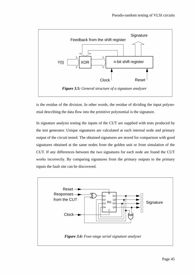
Pseudo-random testing of VLSI circuits
Page 45
is the residue of the division. In other words, the residue of dividing the input polyno-
mial describing the data flow into the primitive polynomial is the signature.
In signature analysis testing the inputs of the CUT are supplied with tests produced by
the test generator. Unique signatures are calculated at each internal node and primary
output of the circuit tested. The obtained signatures are stored for comparison with good
signatures obtained at the same nodes from the golden unit or from simulation of the
CUT. If any differences between the two signatures for each node are found the CUT
works incorrectly. By comparing signatures from the primary outputs to the primary
inputs the fault site can be discovered.
XOR n-bit shift register
Feedback from the shift registerSignature
Clock Reset
Y(t)
Figure 3.5: General structure of a signature analyser
RG
D1
D2
D3
D4
Q2
Q3
Q4
Q1
C
R
Clock
ResetResponsesfrom the CUT
Signature
Figure 3.6: Four-stage serial signature analyser

Pseudo-random testing of VLSI circuits
Page 46
In practice, two basic kinds of signature analysers are used: serial and parallel signature
analysers [28]. A four-stage serial signature analyser and four-stage parallel signature
analyser are shown in Figure 3.6 and Figure 3.7 respectively. A serial signature analyser
treats only one response bit at every clock whereas a parallel signature analyser com-
pacts responses from the outputs of multiple networks under test.
Let us evaluate the probability that an error will not be detected by a signature analyser.
Assume that an input sequence of a given length, say , can be good or faulty at ran-
dom. There are possible signatures which are produced by an -bit signature ana-
lyser. From the set of all possible input sequences of length there are sequences
which map into one signature. Thus, there are error sequences which are
undetectable because they leave the same residue as the correct sequence. This causes
fault masking errors in a signature analyser. The probability of a signature analyser fail-
ing to detect an error can be evaluated by dividing all error sequences which map into
the same signature by the total number of error sequences, i.e.
. For long input sequences, when is large enough,
.
RG
D1
D2
D3
D4
Q2
Q3
Q4
Q1
C
R
Signature
Reset
ClockY1
Y2
Y3
Y4
Figure 3.7: Four-stage parallel signature analyser
m
2n n
m 2n m−
2n m− 1−
P 2m n− 1−( ) 2m 1−( )⁄= m
P 1 2n⁄≈

Pseudo-random testing of VLSI circuits
Page 47
In summary, a signature analyser based on an LFSR can detect all errors in data streams
of or fewer bits, because the entire sequence will remain in the shift register. For long
sequences, whose lengths are more than the LFSR length, the probability of fault mask-
ing errors in a signature analyser depends on the LFSR length. For the 16-bit signature
analyser used by Hewlett Packard . This confirms the high quality of the
signature analysis technique.
n
P 1.5 5−×10=

Page 48
Chapter 4 : Design for testability
of VLSI circuits
4.1 What is design for testability?
It is known that the major parts of testing costs are the cost of test pattern generation and
the cost of test application. Testability is a measure of how easily a VLSI circuit can be
tested to ensure that it performs its intended function. A circuit which can be tested with
less time and effort possesses a greater degree of testability. A circuit which has unde-
tectable faults is untestable and possesses a zero level of testability. Between these two
extremes there are VLSI circuits which have to be tested for long times and/or require
expensive test equipment. Therefore, design for testability (DFT) can be defined as a
design philosophy that leads to decreasing the cost of testing digital circuits and to
increasing the fault coverage or fault isolation.
There are two key concepts in DFT techniques: controllability and observability [32-
35]. Controllability refers to the ease of producing test patterns to the inputs of the sub-
circuit via the primary inputs of the CUT. Observability refers to the ease with which the
responses of the subcircuit can be determined via the primary outputs of the CUT. The
degree of controllability of the circuit can be increased by means of incorporating in it
some additional logic elements and control terminals. The easiest way to increase
observability is to add some extra output terminals into the CUT.
The procedure for designing for testability assumes that modifications of the circuit are
possible to ease the generation and application of test vectors to the circuit to be tested.
To improve testability three groups of DFT techniques have been used: an ad hoc strat-
egy, structured approaches and built-in self-test techniques [33]. There are several basic
criteria which must be taken into account when choosing the most suitable DFT method
for designing a VLSI circuit. These are as follows:
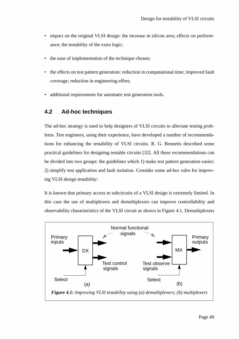
Design for testability of VLSI circuits
Page 49
• impact on the original VLSI design: the increase in silicon area; effects on perform-
ance; the testability of the extra logic;
• the ease of implementation of the technique chosen;
• the effects on test pattern generation: reduction in computational time; improved fault
coverage; reduction in engineering effort;
• additional requirements for automatic test generation tools.
4.2 Ad-hoc techniques
The ad-hoc strategy is used to help designers of VLSI circuits to alleviate testing prob-
lems. Test engineers, using their experience, have developed a number of recommenda-
tions for enhancing the testability of VLSI circuits. R. G. Bennetts described some
practical guidelines for designing testable circuits [32]. All these recommendations can
be divided into two groups: the guidelines which 1) make test pattern generation easier;
2) simplify test application and fault isolation. Consider some ad-hoc rules for improv-
ing VLSI design testability:
It is known that primary access to subcircuits of a VLSI design is extremely limited. In
this case the use of multiplexers and demultiplexers can improve controllability and
observability characteristics of the VLSI circuit as shown in Figure 4.1. Demultiplexers
Select Select
Primaryinputs
Normal functionalsignals
Test controlsignals
Test observesignals
Primaryoutputs
DX MX
(a) (b)
Figure 4.1: Improving VLSI testability using (a) demultiplexers; (b) multiplexers
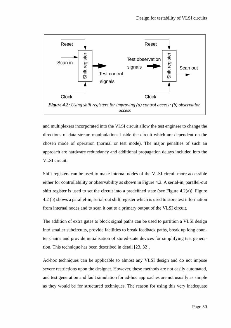
Design for testability of VLSI circuits
Page 50
and multiplexers incorporated into the VLSI circuit allow the test engineer to change the
directions of data stream manipulations inside the circuit which are dependent on the
chosen mode of operation (normal or test mode). The major penalties of such an
approach are hardware redundancy and additional propagation delays included into the
VLSI circuit.
Shift registers can be used to make internal nodes of the VLSI circuit more accessible
either for controllability or observability as shown in Figure 4.2. A serial-in, parallel-out
shift register is used to set the circuit into a predefined state (see Figure 4.2(a)). Figure
4.2 (b) shows a parallel-in, serial-out shift register which is used to store test information
from internal nodes and to scan it out to a primary output of the VLSI circuit.
The addition of extra gates to block signal paths can be used to partition a VLSI design
into smaller subcircuits, provide facilities to break feedback paths, break up long coun-
ter chains and provide initialisation of stored-state devices for simplifying test genera-
tion. This technique has been described in detail [23, 32].
Ad-hoc techniques can be applicable to almost any VLSI design and do not impose
severe restrictions upon the designer. However, these methods are not easily automated,
and test generation and fault simulation for ad-hoc approaches are not usually as simple
as they would be for structured techniques. The reason for using this very inadequate
Clock
Reset
Test control
signals
Clock
Reset
Test observation
signalsScan in
Scan out
Figure 4.2: Using shift registers for improving (a) control access; (b) observationaccess
Shi
ft re
gist
er
Shi
ft re
gist
er

Design for testability of VLSI circuits
Page 51
DFT strategy is due firstly to the fact that the designer does not have the expertise
required for testing and secondly that no effective analysis tools are available to make
good this shortcoming.
4.3 Structured approaches
Although automatic test pattern generators and ad-hoc techniques ease some of the test
problems they cannot ensure the desired degree of controllability and observability at
the structural level for such complicated systems as VLSI circuits. In the mid to late
1970s a number of structural DFT approaches were proposed. Most of these structured
approaches rely on the concept that, if one can control and observe the latch variables
within a sequential circuit, then the test generation problem can be reduced to the testing
of just the combinational logic. The basic structure of the Huffman model for a sequen-
tial network is shown in Figure 4.3. This model includes a number of memory elements,
( ), separated from the combinational logic,CL. The combinational logic
is fed by the primary inputs and the outputs of memory elements placed in the feedback
loops. If all the memory elements could be treated by a straightforward mechanism to
control and observe their states, then the test generation and fault simulation need to be
done only for the combinational logic rather than for the much more difficult case of the
sequential circuit. As a result of considerable research into structured DFT techniques,
MEi 1 i n≤ ≤
Primary
outputs
Primary
inputs
CLME1
ME2
MEn
Figure 4.3: Huffman model for a sequential circuit

Design for testability of VLSI circuits
Page 52
four main formal methods have evolved: scan path [28,34], level-sensitive scan design
[8,13,32], scan/set [9,14] and random access scan [33].
4.3.1 Scan path
The scan path approach assumes that during the test all the memory elements of the
sequential circuit are configured into a long shift register (see Figure 4.4) called the scan
path. All the memory elements of the circuit can be controlled and observed by means of
shifting in and shifting out test data along the path. During normal operation all the stor-
age elements are reconfigured in the way shown in Figure 4.3. The selection of the input
source for the storage elements can be achieved using multiplexed data flip-flops [28] or
two-port flip-flops with two data inputs and two clocks [9].
A scan path technique can be used to partition a VLSI structure into a number of less
complex subcircuits by organizing the scan path to pass through a number of combina-
tional networks. The sequential depth of such a circuit is much less than the depth of the
original one which alleviates the test problem considerably. To test the scan path itself,
flush and shift tests are applied. The flush test consists of all zeros and all ones. The shift
test exercises the memory elements of the scan path through all of their possible combi-
nations of initial and next states.
Shift inEnableshift
Shift out
Primaryinputs
Primary
outputs
RG
CL
Figure 4.4: The principle of scan path techniques

Design for testability of VLSI circuits
Page 53
4.3.2 Level-sensitive scan design
Level-sensitive scan design (LSSD) is based on two main concepts: level sensitivity, and
a scan path. The first assumes that: 1) all changes in the circuit are controlled by the
level of a clock signal; 2) the steady state response of the sequential circuit to an input
state change is independent of the rise and fall times and propagation delays of signals
within the circuit. The second concept of LSSD technique assumes that the circuit must
incorporate a scan path.
Shift register latches (SRL) are used to implement all memory elements in LSSD cir-
cuits. Figure 4.5 shows the symbolic representation of an SRL and its implementation in
NAND gates. In the normal mode of operation clock C3 is not activated and clock C1 is
used to write data to latch L1. Output data can be taken from L1 or, if clock C2 is used,
from L2. In the test operation mode non-overlapping clocks C3 and C2 are used to shift
data from output L2 of the previous SRL into latch L1 (clock C3) with consequent cop-
ying of the data from output L1 into latch L2 (clock C2).
The basic LSSD configuration is illustrated in Figure 4.6. In this structure the pair of two
non-overlapping clocks C1 and C2 are used to store the system data from the combina-
tional logic, CL, in the SRLs (normal operation mode). In the test mode of operation two
sequences of clocks C3 and C2 are applied to control and observe the states of all the
SRLs by means of transferring test data through the scan path (dotted line). Note that
both the L1 and L2 latches participate in the system function and during the test.
Data input (DI)System clock (C1)Scan input (SI)Shift clock (C3)
System/Shift clock (C2)
L1
L2
DI
SI
C2
C1C3
L1
L2
L1
L2
(a) (b)
Figure 4.5: Polarity hold latch (a) symbolic representation; (b) implementation inNAND gates

Design for testability of VLSI circuits
Page 54
The basic algorithm for testing with the LSSD structure shown in Figure 4.6 can be writ-
ten as follows:
• Verify the operation of all the SRLs by applying flush and shift tests.
• Load a test into the SRLs. The test is loaded from the scan-in port of the circuit and
shifted in serially by means of clocks C3 and C2 alternatively activated.
• Generate a test pattern on the primary inputs, PI, of the circuit and turn clock C1 on
and off. As a result, the response of the combinational network is stored in the L1
latches.
• Pulse the system clock C2 to rewrite the contents of the L1 latches into the L2
latches.
• Pulse two sequences of clocks C3 and C2 to scan out the contents of the SRLs. Mean-
while a new test pattern can be loaded into the SRLs.
PI
PO
L1
L1
L1
L2
L2
L2
CL
Scan path
C1
C2
C3Scan in
Scan out
Figure 4.6: LSSD structure
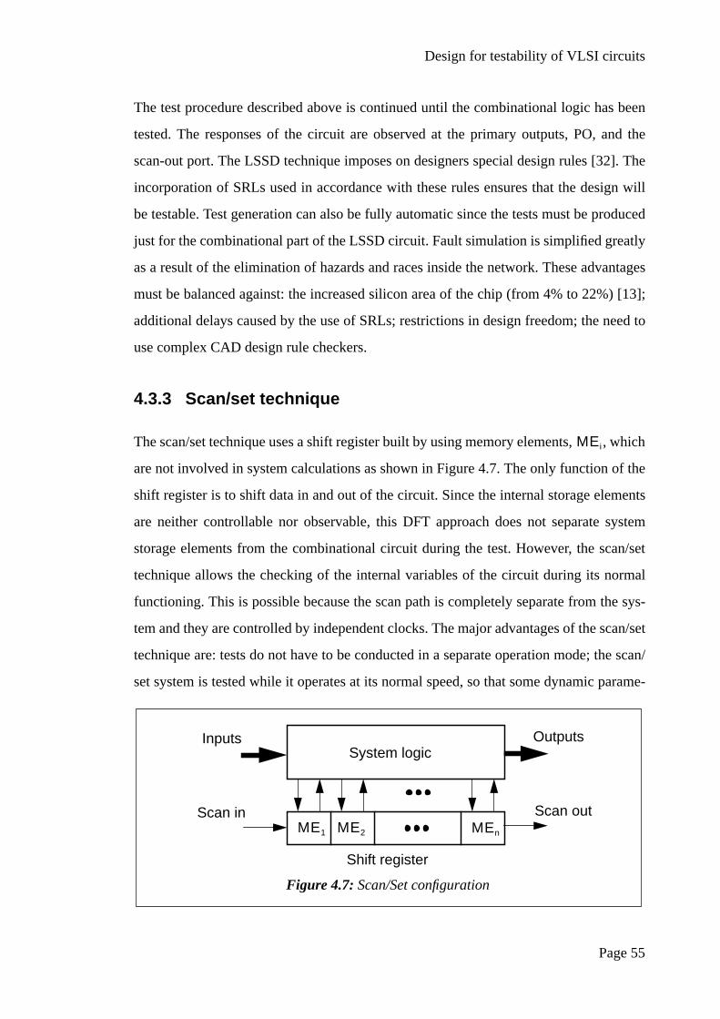
Design for testability of VLSI circuits
Page 55
The test procedure described above is continued until the combinational logic has been
tested. The responses of the circuit are observed at the primary outputs, PO, and the
scan-out port. The LSSD technique imposes on designers special design rules [32]. The
incorporation of SRLs used in accordance with these rules ensures that the design will
be testable. Test generation can also be fully automatic since the tests must be produced
just for the combinational part of the LSSD circuit. Fault simulation is simplified greatly
as a result of the elimination of hazards and races inside the network. These advantages
must be balanced against: the increased silicon area of the chip (from 4% to 22%) [13];
additional delays caused by the use of SRLs; restrictions in design freedom; the need to
use complex CAD design rule checkers.
4.3.3 Scan/set technique
The scan/set technique uses a shift register built by using memory elements,, which
are not involved in system calculations as shown in Figure 4.7. The only function of the
shift register is to shift data in and out of the circuit. Since the internal storage elements
are neither controllable nor observable, this DFT approach does not separate system
storage elements from the combinational circuit during the test. However, the scan/set
technique allows the checking of the internal variables of the circuit during its normal
functioning. This is possible because the scan path is completely separate from the sys-
tem and they are controlled by independent clocks. The major advantages of the scan/set
technique are: tests do not have to be conducted in a separate operation mode; the scan/
set system is tested while it operates at its normal speed, so that some dynamic parame-
MEi
System logic
Scan in Scan out
OutputsInputs
Shift register
Figure 4.7: Scan/Set configuration
ME1 ME2 MEn

Design for testability of VLSI circuits
Page 56
ters of the circuit can be obtained. The internal nodes of the circuit which are to be con-
nected to the shift register are derived from the results of testability analysis programs
[14,28].
4.3.4 Random access scan
The random access scan approach treats each of the latches as a bit of memory as illus-
trated in Figure 4.8. Each element has its own unique address in the addressable space of
the whole memory. There is one common port from which data are loaded into the latch.
The content of each latch is observable for inspection at one output. As a result, the ran-
dom access scan structure reduces the test generation problem to producing tests only
for the combinational logic, CL.
During the test operation mode in random access scan only one latch is activated at a
time to control the internal state of the latch or observe its content. This, in turn, makes
the test procedure slower in comparison to the use of a shift register. Other disadvan-
tages of the random access scan approach are that: 1) it requires high overheads in terms
of additional logic and input/output pins needed to implement the RAM; 2) some con-
straints are imposed on the logic design (for instance, the exclusion of asynchronous
latch operation) [14].
RAM
Address
Inputs Outputs
Scan outScan inCL
Figure 4.8: Random access scan structure
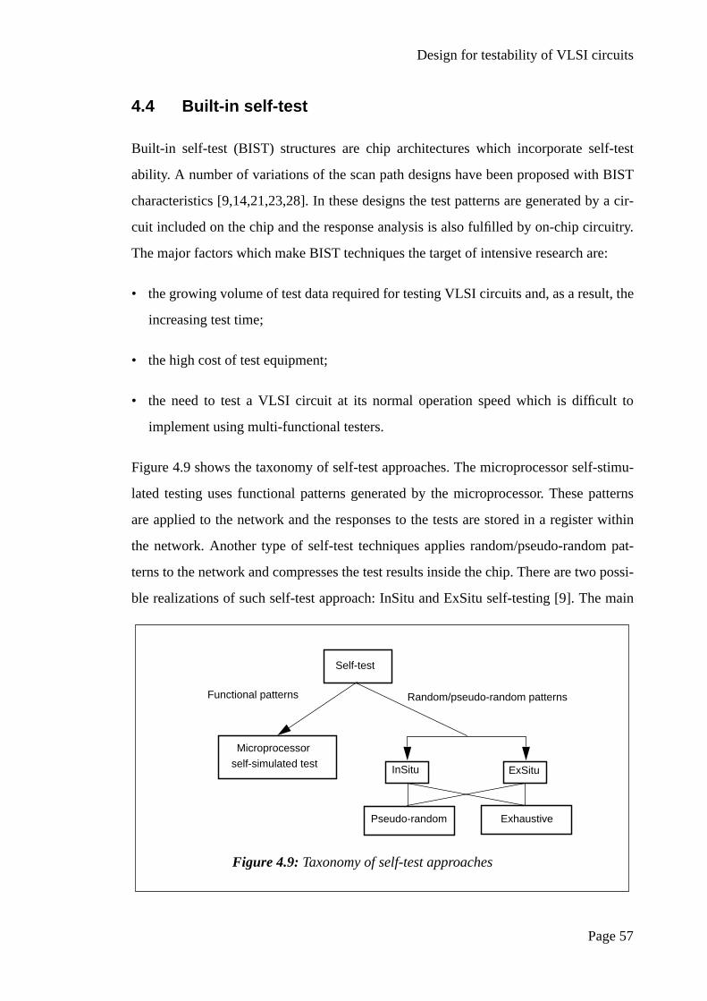
Design for testability of VLSI circuits
Page 57
4.4 Built-in self-test
Built-in self-test (BIST) structures are chip architectures which incorporate self-test
ability. A number of variations of the scan path designs have been proposed with BIST
characteristics [9,14,21,23,28]. In these designs the test patterns are generated by a cir-
cuit included on the chip and the response analysis is also fulfilled by on-chip circuitry.
The major factors which make BIST techniques the target of intensive research are:
• the growing volume of test data required for testing VLSI circuits and, as a result, the
increasing test time;
• the high cost of test equipment;
• the need to test a VLSI circuit at its normal operation speed which is difficult to
implement using multi-functional testers.
Figure 4.9 shows the taxonomy of self-test approaches. The microprocessor self-stimu-
lated testing uses functional patterns generated by the microprocessor. These patterns
are applied to the network and the responses to the tests are stored in a register within
the network. Another type of self-test techniques applies random/pseudo-random pat-
terns to the network and compresses the test results inside the chip. There are two possi-
ble realizations of such self-test approach: InSitu and ExSitu self-testing [9]. The main
Self-test
Microprocessor
self-simulated test InSitu ExSitu
Pseudo-random Exhaustive
Functional patterns Random/pseudo-random patterns
Figure 4.9: Taxonomy of self-test approaches

Design for testability of VLSI circuits
Page 58
difference between these two approaches is that InSitu self-test uses system registers to
generate and compact test data whereas the ExSitu structure uses registers external to
the system function to generate tests and analyse the responses of the circuit.
4.4.1 InSitu self-testing
The classical examples of InSitu self-test are the built-in logic block observation tech-
nique [14] and built-in verification testing [23,31].
Built-in logic block observer
This technique is based on the use of a multi-purpose test module named a “built-in
logic block observer (BILBO)” which can be reconfigured to function as a pseudo-ran-
dom pattern generator or as a signature analyser within a VLSI circuit. The BILBO tech-
nique uses signature analysis in conjunction with a scan path technique. The structure of
a basic 4-bit BILBO element is shown in Figure 4.10. The function of the BILBO ele-
ment is controlled by lines B1 and B2. The storage elements are D-flip-flops. The inputs
of the BILBO element are usually fed by the outputs of the preceding combinational cir-
cuit, the outputs are connected to the inputs of the succeeding combinational network.
There are four modes which can be defined for the BILBO register as follows:
Z1 Z2 Z3 Z4
B1
B2
SDI
Q1 Q2 Q3 Q4
SDO
MX
D1 D2 D3 D4
Figure 4.10: Basic BILBO element

Design for testability of VLSI circuits
Page 59
1. B1=B2=1,System operation mode. The BILBO is configured as a set of D flip-flops
to store system states of a VLSI circuit.
2. B1=B2=0,Shift register mode. The BILBO functions as a long shift register forming a
scan path.
3. B1=1, B2=0, LFSR with multiple inputs. If all the inputs of the BILBO are fixed the
BILBO element shown in Figure 4.10 is configured into the 4-stage PRPG (see Figure
3.3). Otherwise the BILBO functions as the 4-bit parallel signature analyser as shown in
Figure 3.7.
4. B1=0, B2=1,Reset mode. The BILBO register is reset.
Figure 4.11 shows how the BILBO technique can be used to test a VLSI circuit. Initially
one BILBO register works as a PRPG to stimulate the combinational circuit to be tested.
The second BILBO is used as a signature analyser to compress the responses of the cir-
cuit under test. After a certain number of clocks the BILBO register that contained the
signature is reconfigured into a scan path register and the content is shifted out to com-
pare with the signature of the golden unit. The roles of the BILBOs are reversed to test
the next combinational circuit. The above method is called the simplex method of self-
BIL
BO
BIL
BOCombinational
circuit 1
Combinational
circuit 2
BIL
BO
BIL
BOCombinational
circuit 1
Combinational
circuit 2
Pseudo-random Signatureanalyserpattern generator
Pseudo-randompattern generator
Signatureanalyser
Figure 4.11: Self-testing structure with BILBOs
Design for testability of VLSI circuits
Page 60
test. The simlex method is more efficient for self-testing pipelined structures but it has
considerable drawbacks for circuits in which the inputs to one block are formed from the
outputs of many other blocks. In such cases duplex methods must be used where each
functional block has its own PRPG and signature analyser.
There are some networks which are difficult to test by the BILBO technique. For exam-
ple, such circuits as PLAs have a very high ratio of fan-in to logic gates. The probability
of detecting some faults in PLAs can be very low during random testing which causes
the test length to be prohibitively long. Therefore, in order to have this kind of circuit
tested, either deterministic test patterns need to be applied or the circuit must be modi-
fied. Another problem in using the BILBO method lies in the difficulty of calculating
fault free signatures and total fault coverage. The overhead for BILBO is the LSSD or
scan path overhead plus at least one exclusive OR gate per stage of shift register.
Built-in verification testing
This is a technique which applies all possible patterns to the combinational part of the
VLSI circuit. The main principle of verification testing is that if all possible patterns are
applied and the fault mechanism does not change the combinational circuit into a
sequential one, then any faults of the circuit will be detected. During verification testing
every single point in the Karnaugh map is inspected. In the case when every output of a
combinational logic block is not a function of all the inputs, a subset of all possible pat-
terns can be applied to test each subfunction.
The difference between BILBO and verification testing is that the BILBO technique
needs to have a tool to determine the number of random patterns required for random
testing. Also this tool must indicate whether the circuit is testable with random patterns
which is not an easy task [35]. During verification testing, since all possible patterns are
applied to the inputs of the combinational part of the circuit, all faults which are not
redundant will be detected. No special tools are required for such an approach. There is
only one major restriction which is to ensure that there are no redundancies in the net-
work under test.

Design for testability of VLSI circuits
Page 61
4.4.2 ExSitu self-testing
ExSitu BIST structures generate pseudo-random patterns and compact the test results by
means of LFSRs which are not part of the system logic as illustrated in Figure 4.12.
LSSD on-chip self-test
The LSSD on-chip self-test (LOCST) technique has been developed to reduce the vol-
ume of test data to be applied during the random testing of a chip [36]. The basic struc-
ture of the LOCST method is shown in Figure 4.13. The test technique is based on a
scan path approach which uses LSSD latches. There is a special control circuit called the
on-chip monitor, OCM, which monitors the modes of operation of the whole chip.
Pseudo-randomSignature analyser
System logic
Figure 4.12: ExSitu self-testing structure
pattern generator
Enable
Scan in
Scan outOCM
PRPG
SA
Scan path
Scan path
Scan path
Combinationalcircuit
Figure 4.13: LOCST test structure

Design for testability of VLSI circuits
Page 62
In self-test operation mode all the latches of the LOCST design are configured into a
long scan register. The first twenty latches of the design are reconfigured into a PRPG
with maximal length to generate pseudo-random patterns. The last sixteen latches of the
scan path are modified into a signature analyser, SA, to collect test data received from
the scan path register. The reconfigurations of the PRPG and SA are controlled by the
OCM. During self-testing of the chip the pseudo-random sequence generated by the
PRPG is scanned into the scan register. When the register is full the OCM produces a
clock to store the response of the combinational logic into the same register. After that
the content of the scan register is shifted out to the SA. This test cycle is repeated until
the required number of pseudo-random patterns have been applied to the network. At
the end of the test the signature collected into the SA is compared with the good signa-
ture. Clearly, the overall fault coverage of the LOCST technique depends on the extent
of the logic whose inputs and outputs can be accessible by using the scan latches. The
OCM and any embedded RAMs of the chip can not be tested by the LOCST technique.
The main disadvantage of this self-test method is that the test time proportionally
depends on the length of the scan path. As a result, the LOCST technique cannot be used
for any VLSI design with an arbitrary number of memory elements.
STUMPS approach
The major disadvantage of the LOCST self-test technique can be overcome if the PRPG
is reconfigured to supply several scan path registers with pseudo-random patterns in par-
allel. The test data obtained from these registers are compressed using a parallel signa-
ture analyser. Such a self-test approach was named the STUMPS approach [37]. The
general structure of the STUMPS approach is shown in Figure 4.14.
This technique drives the scan paths of LSSD chips. Once all the shift registers are
loaded a system clock is activated so that the test results are stored in some of the SRLs
on the chips. This data is then off-loaded into the parallel signature analyser. The time of
testing such design depends on the length of the longest scan path.

Design for testability of VLSI circuits
Page 63
4.5 Summary
It is clear that one particular DFT method cannot solve all the problems concerned with
testing VLSI circuits. Each DFT technique can solve only a subset of test problems with
the help of increasing the degree of testability of the VLSI circuit to be tested. The most
widely used DFT systems use a reconfigurable structure which permits the combina-
tional logic and the memory elements to be separated for test purposes. The combina-
tional circuit is tested in isolation. All the memory elements are formed into a long shift
register or RAM to feed the inputs of the combinational network with tests and store the
responses for inspection as in the case of scan path techniques. Self-test methods allow
the generation and compression of test data inside a chip which alleviates the problem of
operating with a large amount of test data.
The advantages of DFT methods for VLSI circuits are not achieved without a cost meas-
ured usually in terms of silicon overhead. Estimates vary typically from 4% to 20%. The
true figure for the silicon overhead for a particular DFT approach is not easy to derive
because it depends on many factors such as the structural characteristics of the VLSI cir-
cuit, the desired test time, test generation methods and so on. Performance degradation
Pseudo-random pattern generator
Parallel signature analyser
Chi
p 1
Chi
p 2
Chi
p N
SRLs
1
2
m
1
2
n
1
2
k
Figure 4.14: ExSitu STUMPS approach

Design for testability of VLSI circuits
Page 64
and reduction in reliability due to extra components in the signal path are other serious
penalties of using DFT methods. The justification for incurring these or other costs of
DFT lies in the savings in test-related costs.

Page 65
Chapter 5 : Testing asynchronous
VLSI designs - related
works
5.1 Problems with testing asynchronous VLSI circuits
Despite the essential advantages of using asynchronous designs the testing of asynchro-
nous VLSI circuits remains a difficult problem due to the following reasons:
• asynchronous circuits often include races and are susceptible to incorrect operation
due to hazards;
• to derive an iterative model for the circuit it is necessary to identify all feedback
wires which requires an expensive analysis of the topology of the circuit;
• the correctness of the asynchronous circuit often depends on delays incorporated into
the circuit, whereas the most test generation algorithms ignore delays;
• most asynchronous designs use a certain amount of hardware redundancy to avoid
hazards, which compromises testability;
• the absence of a global clock makes the application of test techniques for combina-
tional circuits hard to adapt to the testing of sequential circuits;
• asynchronous designs use a large number of storage elements (such as Muller-C ele-
ments, toggles etc.) which do not allow the use of DFT techniques due to the prohib-
itively large extent of the resulting hardware redundancy.
The publications devoted to the testing of asynchronous designs can be classified
according to the objects under test. The first group deals with testing bounded-delay
asynchronous circuits, the second one considers some possible solutions to the testing of

Testing asynchronous VLSI designs - related works
Page 66
delay-insensitive circuits, and the third group of works is devoted to the problem of test-
ing speed-independent asynchronous designs. This chapter is structured accordingly.
Although micropipelines are inherently bounded-delay asynchronous circuits, the issues
in the fault simulation and testing of micropipelines are discussed in the last section of
the chapter since this is the main topic of this thesis.
5.2 Testing bounded-delay circuits
The most obvious model to use for asynchronous circuits is the Huffman model for dig-
ital networks which is widely used for designing synchronous circuits. To design an
asynchronous circuit it is assumed that the delays of all the logic elements and wires are
known in this model, or at least bounded. The same techniques of designing combina-
tional circuits are used to build combinational networks in asynchronous VLSI systems.
All static and dynamic hazards must be removed by adding extra logic elements [4].
Bounded-delay asynchronous circuits complicate the fault detection procedure. The
adding of redundant terms to functions to eliminate hazards is in direct conflict with the
fault testing technique which requires the avoidance of redundant terms to make faults
visible [11]. The Huffman model for synchronous sequential circuits shown in Figure
4.3 can be used for designing bounded delay asynchronous circuits. Since we need to
make sure that the combinational logic has settled in response to a new input before the
present-state entries change, all the memory elements must be replaced by delay ele-
ments.
G. R. Putzolu and J. P. Roth have described an algorithm for generating tests to detect
stuck-at faults in asynchronous sequential logic circuits [38]. This algorithm is based
upon an extension of the D-algorithm. A general view of an asynchronous sequential
circuit S was considered. It was assumed that a stuck-at faultF modifies only the logical
function ofS. The basic test strategy proposed consists of the following steps:
1) to transform the detection procedure of faultF in S into the detection of a correspond-
ing set of faults in an iterative combinational logic circuit derived fromS;Fr Cr
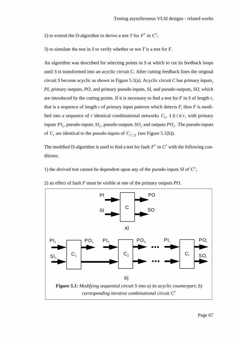
Testing asynchronous VLSI designs - related works
Page 67
2) to extend the D-algorithm to derive a testT for in ;
3) to simulate the test inS to verify whether or notT is a test forF.
An algorithm was described for selecting points inS at which to cut its feedback loops
until S is transformed into an acyclic circuitC. After cutting feedback lines the original
circuit S become acyclic as shown in Figure 5.1(a). Acyclic circuitC has primary inputs,
PI, primary outputs,PO, and primary pseudo-inputs,SI, and pseudo-outputs,SO, which
are introduced by the cutting points. If it is necessary to find a test forF in S of lengthr,
that is a sequence of length r of primary input patterns which detectsF, thenF is modi-
fied into a sequence ofr identical combinational networks , , with primary
inputs , pseudo-inputs , pseudo-outputs and outputs . The pseudo-inputs
of are identical to the pseudo-inputs of (see Figure 5.1(b)).
The modified D-algorithm is used to find a test for fault in with the following con-
ditions:
1) the derived test cannot be dependent upon any of the pseudo-inputsSI of ;
2) an effect of faultF must be visible at one of the primary outputsPO.
Fr Cr
Ci 1 i r≤ ≤
PIi SIi SOi POi
Ci Ci 1+
C
PI
SI
PO
SO
PI1 PI2 PIr
SI1
PO1 PO2 POr
SOrC1 C2 Cr
a)
b)
Figure 5.1: Modifying sequential circuit S into a) its acyclic counterpart; b)
corresponding iterative combinational circuit Cr
Fr Cr
Cr

Testing asynchronous VLSI designs - related works
Page 68
As a result, the test consists of an ordered set ofr input patterns applied to the primary
inputsPI of S. After that the behaviour ofS is simulated while applying the derived set
of patterns. If during the simulation no races or hazards are registered inS, then the test
is accepted as a test for faultF in S.
The main drawbacks of this test generation algorithm are that:
1) it requires an extended analysis of the topology of the circuit to be tested;
2) it cannot guarantee the derivation of a race and hazard free test.
S. G. Chappell has proposed another approach to testing bounded-delay asynchronous
circuits [39]. In this method Boolean equations are developed for the outputs of the cir-
cuit in terms of sequences of signals. The circuit model treats logic circuits as intercon-
nections of unit- and zero-time-delay logic elements. The main features of this approach
are:
1) all test sequences for detecting a specific fault can be derived;
2) some race conditions can be dealt with;
3) feedback lines need not be identified in the circuit.
The test generation algorithm is represented by the following steps:
1. Set the maximum sequence lengthm=1.
2. Generate equations for the circuit under test with sequence length m.
3. Obtain tests using maximum-cover strategy.
4. Simulate the derived tests. If the percentage of undetected faults is less then 10% then
go to step 5. Otherwise, setm=m+1 and return to step 2.
5. Generate tests for remaining faults detectable with sequence length m.

Testing asynchronous VLSI designs - related works
Page 69
6. If the percentage of undetected faults is less or equal to the desired fault coverage then
stop. Otherwise, setm=m+1 and return to step 5.
The technique generates two equations denoted as and for each logic ele-
ment in the circuit. These equations determine the input conditions required to set gateF
to logical 0 and 1 respectively at timet. The technique starts from the circuit inputs and
proceeds forward through the circuit. As a result, it is not necessary to identify feedback
lines and combinational and sequential circuits can be treated by the same algorithm.
The sequence length of the test indicates the number of input patterns required to detect
a fault and propagate the fault effect to an output of the circuit. To generate all tests for a
combinational circuit a sequence length of one is sufficient. Figure 5.2 shows an exam-
ple of an R-S flip-flop which is realized using NAND gates. Let and
denote logical 0 and 1 respectively on input linea during theith vector of the sequence.
The algorithm for deriving equations for an R-S flip-flop from an unknown state is
shown in Table 5.1. It is assumed that in the initial state .
The inputs are applied at timet. Only and changed values at timet+1. As a con-
sequence, only and are calculated at timet+2. At time t+3, none of the output
equations changed which means that the flip-flop has reached its stable state and compu-
tation stops. Similar computations can be carried out if the circuit is in a known initial
state.
Equations for faulty circuits can be derived in the same way as for fault-free circuits.
This approach allows the generation of tests for detecting stuck-at faults in asynchro-
nous circuits. Faults in circuits are represented by fault variables and which
F0 t( ) F1 t( )
a0 i( ) a1 i( )
F0 F1 G0 G1 0= = = =
F1 G1
G0 F0
F
G
a0 a1,( )
b0 b1,( )
Figure 5.2: R-S flip-flop realized using NAND gates
x0 i, x1 i,
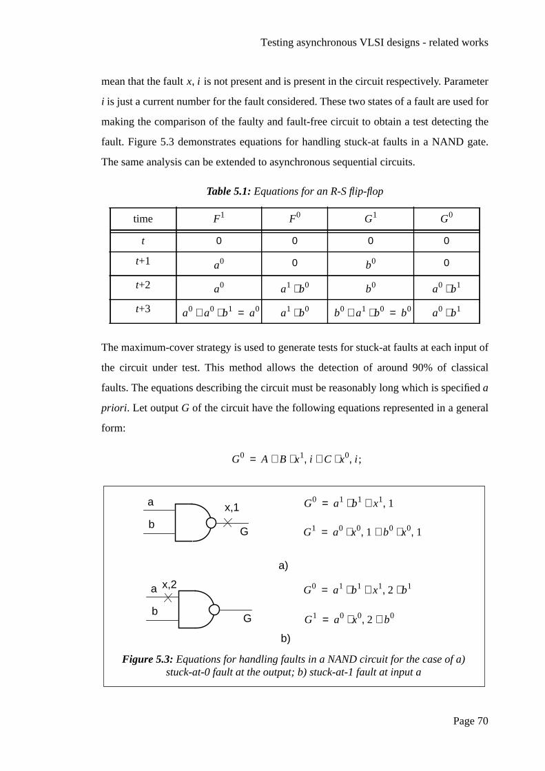
Testing asynchronous VLSI designs - related works
Page 70
mean that the fault is not present and is present in the circuit respectively. Parameter
i is just a current number for the fault considered. These two states of a fault are used for
making the comparison of the faulty and fault-free circuit to obtain a test detecting the
fault. Figure 5.3 demonstrates equations for handling stuck-at faults in a NAND gate.
The same analysis can be extended to asynchronous sequential circuits.
The maximum-cover strategy is used to generate tests for stuck-at faults at each input of
the circuit under test. This method allows the detection of around 90% of classical
faults. The equations describing the circuit must be reasonably long which is specifieda
priori . Let outputG of the circuit have the following equations represented in a general
form:
;
Table 5.1: Equations for an R-S flip-flop
time
t 0 0 0 0
t+1 0 0
t+2
t+3
x i,
x,1a
bG
G0 a1 b1⋅ x1 1,+=
G1 a0 x0 1 b0 x0 1,⋅+,⋅=
x,2a
bG
a)
b)
G0 a1 b1⋅ x1 2, b1⋅+=
G1 a0 x0 2 b0+,⋅=
Figure 5.3: Equations for handling faults in a NAND circuit for the case of a)stuck-at-0 fault at the output; b) stuck-at-1 fault at input a
F1 F0 G1 G0
a0 b0
a0 a1 b0⋅ b0 a0 b1⋅
a0 a0 b1⋅+ a0= a1 b0⋅ b0 a1 b0⋅+ b0= a0 b1⋅
G0 A B x1 i,⋅ C x0 i,⋅+ +=

Testing asynchronous VLSI designs - related works
Page 71
,
whereA, ...,F are also sum-of-products expressions. The tests to detect faultx,i at out-
putG are defined by . The basic idea of the maximum-cover strategy is that
tests for all stuck-at faults on the primary input lines can also detect some other (inter-
nal) stuck-at faults of the circuit. For this purpose the output equations are factored as
before, i.e.
;
.
Tests for faultj on inputa are derived from the following expression:
.
This expression, except for specifying the propagation conditions of the fault, deter-
mines the value to be assigned to input linea. The main drawback of the test generation
technique described above is that it requires the detailed examination of the circuit to be
tested. This leads to the computation time for the derivation of tests for VLSI designs
increasing prohibitively.
A general description of asynchronous sequential circuits and their testability problems
has been given by B. J. Heard [40]. A set of hardware modification techniques is
described which allows asynchronous VLSI circuits to be tested by scan techniques. The
use of special simulation techniques for flip-flops allows the generation of tests for asyn-
chronous circuits on the basis of the D-algorithm. Two types of asynchronous designs
were considered: circuits in which there is at least one flip-flop providing an asynchro-
nous set/reset input to another flip-flop; circuits which contain at least one flip-flop pro-
viding the clock input to another flip-flop.
Figure 5.4a illustrates an example of an asynchronous reset network. This circuit cannot
be tested by conventional scan techniques because:
G1 D E x1 i,⋅ F x0 i,⋅+ +=
B F⋅ C E⋅+
F0 A B a1 j,⋅ C a0 j,⋅+ +=
F1 D E a1 j,⋅ F a0 j,⋅+ +=
B F⋅ C E⋅+( ) a1 j a0 j,+,( )⋅

Testing asynchronous VLSI designs - related works
Page 72
1) the asynchronous input can be activated while the test data are being loaded into the
flip-flops of circuit 2 which can alter the data shifted into the D flip-flop;
2) the asynchronous input is sensitive to hazards which can take place on the output of
circuit 2 during the test which, in turn, can change the response stored into the D flip-
flop.
Figure 5.4b shows a solution which allows the asynchronous network to be made testa-
ble. The asynchronous control clock is controlled independently. When the asynchro-
nous control clock is asserted to a logic one the synchronous logic (circuit 1) can be
tested using scan methods. The asynchronous logic is tested when the system clock is
held steady while the asynchronous control clock is pulsed. A set of software simulation
Sequential circuit 1
Sequential circuit 2
D Q
Reset
Sequential circuit 1
Sequential circuit 2
D Q
Reset
Asynchronouscontrol clock
a) b)
Figure 5.4: An example of untestable a) and testable b) asynchronous reset network
D Q
Reset
D Q D Q
Reset
D Q
Figure 5.5: Testing asynchronous reset network: a) synchronous model; b)asynchronous model
a) b)

Testing asynchronous VLSI designs - related works
Page 73
programs is proposed to generate tests for asynchronous set/reset circuits. The model
shown in Figure 5.5a is used to simulate the synchronous test procedure. For simulating
asynchronous testing, the model shown in Figure 5.5b is used.
This method for testing asynchronous circuits is oriented to the detection of only stuck-
at faults and cannot solve the problem of identifying timing relationships between asyn-
chronous signals inside asynchronous networks. The performance of such testable asyn-
chronous circuits is affected by the extra delays of set/reset and clock lines. As a result,
the designer must take into consideration the effects of these extra delays when calculat-
ing the timing characteristics of the circuit.
T. Fujieda and N. Zenke have described an original method for testing such asynchro-
nous VLSI devices as Video RAMs, Dual Port RAMs and FIFOs [41]. The problem of
testing these circuits is that they have two or more ports operating at different frequen-
cies asynchronously and simultaneously. Conventional test methods are not able to
check the asynchronous operation of multiple ports properly. The new method proposed
allows the testing of two ports simultaneously and asynchronously by means of using
the test system which includes two pattern generators and two timing generators.
An attempt to implement boundary-scan and pseudo-random BIST in an asynchronous
transfer mode switch has been made [42]. The asynchronous transfer switch mode is
capable of switching up to Gbit/s. The switching function is essentially com-
posed of a Double Access RAM which stores the incoming cells under supervision of a
control circuit. Two types of faults in the Double Access RAM were considered imple-
mented in CMOS technology:
1) stuck-open faults;
2) simultaneous reading and writing faults.
The proposed approach allows the detection of these faults during the test operation
mode with fault coverage of 99.9%. During testing, all addresses and input stimuli are
16 1.244×
Testing asynchronous VLSI designs - related works
Page 74
produced by a PRPG and the responses are collected into a signature analyser. A special
register was developed for testing the Double Access RAM.
C. Bellon and R. Velazco have proposed a behavioural test method for programmable
circuits [43]. This method is based upon the notion of behavioural sequential machines
and the identification principle. They described a system for automated generation of
test programs for microprocessors. The system, besides generating tests, is capable of
making a composition of timing diagrams of test signals. This simplifies testing such
asynchronous functions of a microprocessor as interrupts caused by peripheral circuits.
The major disadvantage of the test approaches described above is that they were devised
to test only special purpose asynchronous circuits and asynchronous functions inside
synchronous designs. A set of formal methods was proposed to design testable asyn-
chronous sequential circuits [44-46]. A. K. Susskind proposed to add one or at most two
state variables, one extra input and to use one or more observable outputs in order to
make the sequential circuit under test strongly connected and testable through scan-out
features [44]. An asynchronous sequential network is strongly connected if any stable
state can be reached from any other state. The scan-out technique is applied directly to
the flow table describing the asynchronous sequential circuit to be tested. The test proce-
dure proposed is based on verifying the flow table of the circuit under test. As a result,
no fault models are used. The use of this approach is limited by the complexity of the
circuit to be tested and becomes impractical for asynchronous VLSI circuits. The test
technique does not guarantee both hazard-free operation and hazard-free robust path-
delay-fault testability of asynchronous circuits. K. Keutzer, L. Lavagno and A. Sangio-
vanni-Vincentelli have described some heuristic techniques and procedures to design
asynchronous circuits which are simultaneously hazard-free, robust path-delay-fault
testable and hazard-free in operation [46]. The synthesis of asynchronous sequential cir-
cuits is performed using a high level specification, the signal transition graph. Using an
appropriate delay model it is possible to design asynchronous circuits which are hazard-
free. The test procedure uses scan techniques for applying each pair of test vectors to
detect an appropriate path-delay-fault in a robust and hazard-free manner. In such asyn-

Testing asynchronous VLSI designs - related works
Page 75
chronous circuits every latch can be scanned to increase controllability and observability
of its inputs and outputs. It was shown that there is a negligible area or delay penalty
required to achieve robust path-delay-fault testability. Nevertheless, the test approach
imposes strict limitations on the speed at which the circuit can be tested.
5.3 Testing delay-insensitive circuits
P. Hazewindus made a successful proposal to adapt known test generation algorithms
for testing delay-insensitive circuits using stuck-at fault model [47]. A technique to test
delay-insensitive circuits was synthesized from a high-level specification. It used the
high-level synthesis method for delay-insensitive circuits that was developed by A. J.
Martin [6]. Two types of stuck-at faults in delay-insensitive circuits were considered:
faults that cause the circuit to halt entirely, and faults which change the output of the cir-
cuit. The last kind of fault is either a stimulating or an inhibiting fault. The stuck-at fault
is stimulating if this fault in a delay-insensitive circuit causes a production rule to fire
when it should not. If a stuck-at fault in a delay-insensitive circuit may cause a produc-
tion rule not to fire when it should then the fault is identified as inhibiting. It was
assumed that the delay-insensitive circuits to be tested are non-redundant. In such a case
for each inhibiting fault there is a state in the handshaking expansion where the fault
causes a transition not to take place when it should; for each stimulating fault there is a
state in the handshaking expansion where the fault causes a transition to occur when it
should not. Thus, the testing algorithm is to force the faulty circuit to go in such a state
(the state where the fault manifests itself) and to propagate the fault to an observable
output of the circuit under test.
A combinational logic in a synchronous design is a feedback-free network of logic ele-
ments which calculates a function of the primary inputs. There are similar feedback-free
delay-insensitive circuits which make their computations without buffering the result,
although they contain state-holding elements. It was shown that any delay-insensitive
circuit in which:
1) there are no feedback lines at the gate level;
Testing asynchronous VLSI designs - related works
Page 76
2) each production rule for an up-transition (down-transition) has only positive (nega-
tive) literals in its guard;
can be reduced to a standard combinational logic circuit to ease the testing procedure.
This combinational network is monotonic, and any test which detects all testable faults
in this network will also detect all testable faults in the delay-insensitive circuit.
The standard D-algorithm can be extended to obtain a test pattern for a stuck-at fault in a
delay-insensitive combinational circuit. Regular forward and backward propagation
techniques can be used for such circuits. The major difference with combinational cir-
cuits is that there are some state-holding elements in delay-insensitive combinational
circuits. It is necessary to take into consideration whether the circuit is in an up-going or
a down-going phase for propagating a fault through a state-holding element.
Forward propagation. Let S be a state-holding element. Transform S into by replac-
ing the guard for the down-transition with the negation of the guard for the up-transition.
Gate is a combinational gate and is equivalent to S during the up-phase. Thus, the
propagation of D and is the same for S as for . For instance, if S is a C-element,
then is an AND gate. During a down-phase, S propagates a faulty signal if the output
of the gate is 1 after the up-phase. Transform S into by replacing the guard for the up-
transition with the negation of the guard for the down-transition. Then is a combina-
tional gate which is equivalent to S during the down-phase, if the output of S is 1 after
the up-phase. The propagation of D and is the same for S as for . If S is a C-element
then is an OR gate.
Backward propagation. Transform S into for the up-phase and for the down-
phase. The backward propagation for these combinational circuits is the same as it was
described before. If S is a C-element with output D then all its inputs must be 1 for
detection during an up-phase, and at least one input is 1 for detection during a down-
phase. If the output is then during an up-phase at least one input is 0; during a down-
phase all the inputs are 0.
Su
Su
D Su
Su
Sd
Sd
D Sd
Sd
Su Sd
D
Testing asynchronous VLSI designs - related works
Page 77
Design for testability problems for delay-insensitive circuits were discussed. It was
shown that each fault in a delay-insensitive circuit can be made testable by means of the
addition of test points. These test points can be either control or observation points. If a
premature firing is unstable then a control point is needed; if the premature firing is not
propagated to a primary output then an observation point is needed. It was shown how to
find a place where a test point must be inserted. For VLSI circuits which are pad-limited,
it was proposed to merge the test points together into a queue. A fully testable design for
such a test queue was derived.
The test approach for delay-insensitive circuits described above is efficient enough only
for circuits of reasonable complexity, and becomes impractical for delay-insensitive
VLSI circuits. Roncken and Saeijs have proposed a test strategy which can be integrated
with the design of VLSI circuits through silicon compilation [48]. The strategy is based
on a simple test procedure for which circuits are enhanced with a special mode of opera-
tion. As a result, the test generation time is linear in the size of the VLSI circuit.
5.4 Testing speed-independent networks
The problem of testing speed-independent circuits has already been addressed [49-50].
It was shown that live speed-independent circuits, which are strongly connected and
composed of AND gates, OR gates and C-elements can be decomposed into a set of
semi-modular networks. As a result, these circuits are self-checking with respect to cer-
tain classes of output stuck-at faults and input stuck-at faults. A live speed-independent
circuit is a circuit whose signal graph is live, i.e. the signal graph is strongly connected
and every transition of every signal is enabled in some valid state. A speed-independent
circuit is semi-modular if its signal graph contains only transitions which do not disable
other transitions.
The self-checking property of speed-independent circuits is due to the fact that a stuck-
at fault can be considered as an infinite delay. Thus, a circuit whose operation depends
on that delay will halt in the presence of that fault. Unfortunately, the class of faults for

Testing asynchronous VLSI designs - related works
Page 78
which the self-checking property can be used for testing purposes is very limited and
can hardly represent real faults in speed-independent circuits.
5.5 Testing micropipelines
One of the most detailed considerations of the problems of testing micropipelines has
been made by Pagey, Sherlekar and Venkatesh [51]. It was noted that micropipelines
have some advantages which make them easy to test. These are:
• the control circuits of the micropipeline are tested during normal operation mode;
• test generation for the data path of the micropipeline can be reduced to testing only
combinational logic by means of minor changes in test operation mode;
• testing latches can be done by applying only two-pattern tests which can be generated
using test generation techniques for combinational networks.
The single stuck-at fault model on all the lines (either logic or control lines) in the
micropipeline was considered. Three classes of faults for the micropipeline were identi-
fied:
• faults in the control part of the micropipeline;
• faults in logic blocks;
• faults in the latches.
It was assumed that a stuck-at fault inside the latch can put a register bit of the latch in
capture (stuck-at-capture fault) or pass (stuck-at-pass fault) mode permanently. The
analysis of behaviour of the C-element was made in the presence of single stuck-at
faults.If a stuck-at-1 or stuck-at-0 fault is present on the output of the Muller C-element
then the Muller C-element remains in this state. If the Muller C-element was previously
set to 1 (0) and there is stuck-at-0 (stuck-at-1) fault on one of its inputs then only one
transition ( ) can occur on the output of the Muller C-element.1 0→ 0 1→

Testing asynchronous VLSI designs - related works
Page 79
Faults in the control part of the micropipeline
These are faults on the inputs and outputs of the Muller C-elements and the request and
acknowledge lines of the micropipeline. Any stuck-at fault on a request or acknowledge
line causes the micropipeline to halt since no events are produced in the control part of
the micropipeline. As was shown above, any stuck-at fault on the inputs or the output of
the Muller C-element allows at most one event to be generated on the output of the
Muller C-element. As a result, in the presence of a stuck-at fault in the control part, the
micropipeline advances through at most one step and then halts. Thus, stuck-at faults in
the control part of the micropipeline manifest themselves by preventing activity in the
micropipeline.
Faults in the logic blocks
If it is possible to set all the latches of the micropipeline in the pass mode then all logic
elements can be treated as a single combinational logic block (see Figure 1.5). To detect
any of the single stuck-at faults in such combinational logic test vectors can be obtained
using any known test generation technique for combinational circuits. Therefore, the test
procedure for the micropipeline contains two major steps:
1) the micropipeline is emptied, i.e. all the latches are set in the pass mode;
2) the test vectors are applied to the inputs of the micropipeline and the responses of the
micropipeline are compared with good responses.
Faults in the latches
It is assumed that the combinational logic obtained after the latches have been set in the
pass mode has no redundant faults. Figure 5.6 shows an example of an implementation
of the event controlled latch. An event generated on the dotted line inside the latch
causes a switch between two modes of the latch: pass and capture.
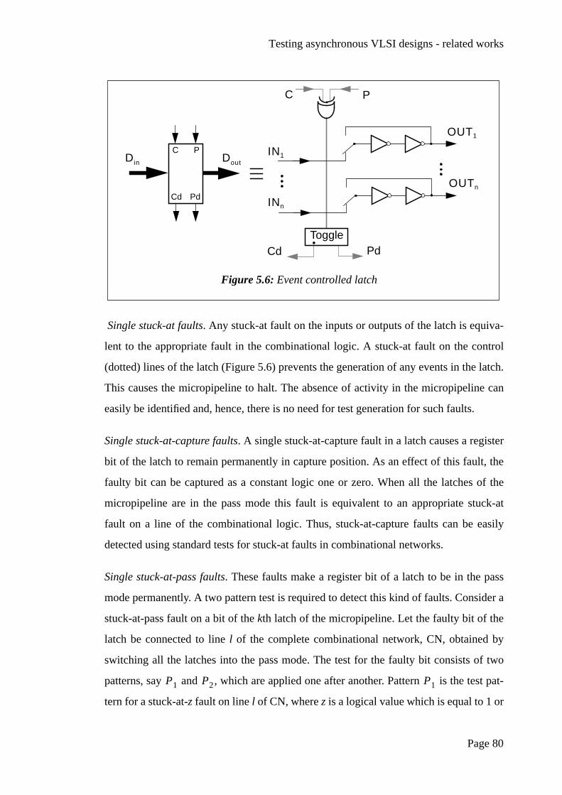
Testing asynchronous VLSI designs - related works
Page 80
Single stuck-at faults. Any stuck-at fault on the inputs or outputs of the latch is equiva-
lent to the appropriate fault in the combinational logic. A stuck-at fault on the control
(dotted) lines of the latch (Figure 5.6) prevents the generation of any events in the latch.
This causes the micropipeline to halt. The absence of activity in the micropipeline can
easily be identified and, hence, there is no need for test generation for such faults.
Single stuck-at-capture faults. A single stuck-at-capture fault in a latch causes a register
bit of the latch to remain permanently in capture position. As an effect of this fault, the
faulty bit can be captured as a constant logic one or zero. When all the latches of the
micropipeline are in the pass mode this fault is equivalent to an appropriate stuck-at
fault on a line of the combinational logic. Thus, stuck-at-capture faults can be easily
detected using standard tests for stuck-at faults in combinational networks.
Single stuck-at-pass faults. These faults make a register bit of a latch to be in the pass
mode permanently. A two pattern test is required to detect this kind of faults. Consider a
stuck-at-pass fault on a bit of thekth latch of the micropipeline. Let the faulty bit of the
latch be connected to line l of the complete combinational network, CN, obtained by
switching all the latches into the pass mode. The test for the faulty bit consists of two
patterns, say and , which are applied one after another. Pattern is the test pat-
tern for a stuck-at-z fault on linel of CN, wherez is a logical value which is equal to 1 or
Toggle
C P
Cd Pd
IN1
INn
OUT1
OUTn
C
Cd
P
Pd
Din Dout
Figure 5.6: Event controlled latch
P1 P2 P1

Testing asynchronous VLSI designs - related works
Page 81
0. Pattern is the test vector which forces linel to be set to logical valuez. These test
patterns can be obtained easily by means of standard test generation methods for combi-
national circuits.
The test procedure for detecting a stuck-at-pass fault in the micropipeline is the follow-
ing:
1. Apply pattern to the inputs of the micropipeline while all the latches are in the
pass mode. Put thekth latch in the capture mode. As a result, linel has been set to logic
. The response is observed at the outputs of the micropipeline.
2. Apply pattern to the inputs of the micropipeline. Thus, linel of CN has been
driven to logicz since the faulty bit of the latch is connected to linel of CN; other lines
of the latch are at their logical values corresponding to pattern. This causes at least
one output of the micropipeline to be different from the fault-free response.
The result described above is the starting point in researching possible test approaches
for micropipelines. The preliminary results show that tests for the single stuck-at type
fault model can be generated using known test generation algorithms for combinational
circuits. Problems which must be solved are
• designing appropriate methods for transferring the micropipeline from the normal
operation mode to the test mode;
• testing delay faults either in CN or individual logic blocks;
• designing for testability.
P2
P1
z
P2
P1

Page 82
Chapter 6 : Asynchronous
random testing
interface
Although DFT methods give test engineers a great opportunity to simplify the testing of
either synchronous or asynchronous VLSI designs, test generation and fault simulation
costs are still large and are rising with the increasing complexity of VLSI circuits. As a
result, random testing becomes a viable alternative for testing asynchronous VLSI
devices for at least two reasons:
• As shown in the previous chapters test generation methods for asynchronous VLSI
circuits are more complicated than for synchronous ones, whereas the use of pseudo-
random pattern generators (PRPG) for the random testing of VLSI circuits does not
require any special properties from the CUT except that it does not have illegal input
combinations.
• It is possible to use pseudo-random test patterns in asynchronous BIST VLSI struc-
tures.
Some asynchronous realizations of a PRPG and a signature analyser with the two-phase
transition signalling communication protocol and a general description of software tools
for simulating the behaviour of the universal PRPG are presented in this chapter.
6.1 Asynchronous implementations of PRPG and signature
analyser
As asynchronous VLSI circuits perform their functions asynchronously the test proce-
dure must be organized in the same (asynchronous) manner to correspond to the same
asynchronous communication protocol between the CUT and test equipment. There are

Asynchronous random testing interface
Page 83
three major components in the random test procedure: PRPG, CUT and parallel signa-
ture analyser (see Figure 6.1). All the components of the structure operate using the two-
phase bundled data convention mechanism. Test patterns are generated by the PRPG and
the responses of the CUT are collected by the parallel signature analyser, PSA.
6.1.1 Asynchronous PRPG
The simplest way to realize an asynchronous version of the PRPG is the use of the syn-
chronous PRPG which is clocked by the special asynchronous circuitry as illustrated in
Figure 6.2. In the initial state the PRPG is set to the non-zero initial state and all the
other lines of the asynchronous circuitry are set to logical zeros. As a result, the asyn-
chronous PRPG produces a request signal on its output R(out). After receiving an
acknowledge signal on its input A(out) the rising edge of the clock signal is generated
CUTPRPG PSA
R(in) R(out)
A(in) A(out)
Request
Acknowledge
Request
Acknowledge
R(out)
A(out) A(in)
R(in)
Data(in) Data(out)
Figure 6.1: Asynchronous random testing interface with the two-phase bundleddata convention
R(out)
A(out)
C
Togg
le
delay
Clk
PRPG
Set
Set
A(out) R(out)
Data
Figure 6.2: An asynchronous version of a pseudo-random pattern generator
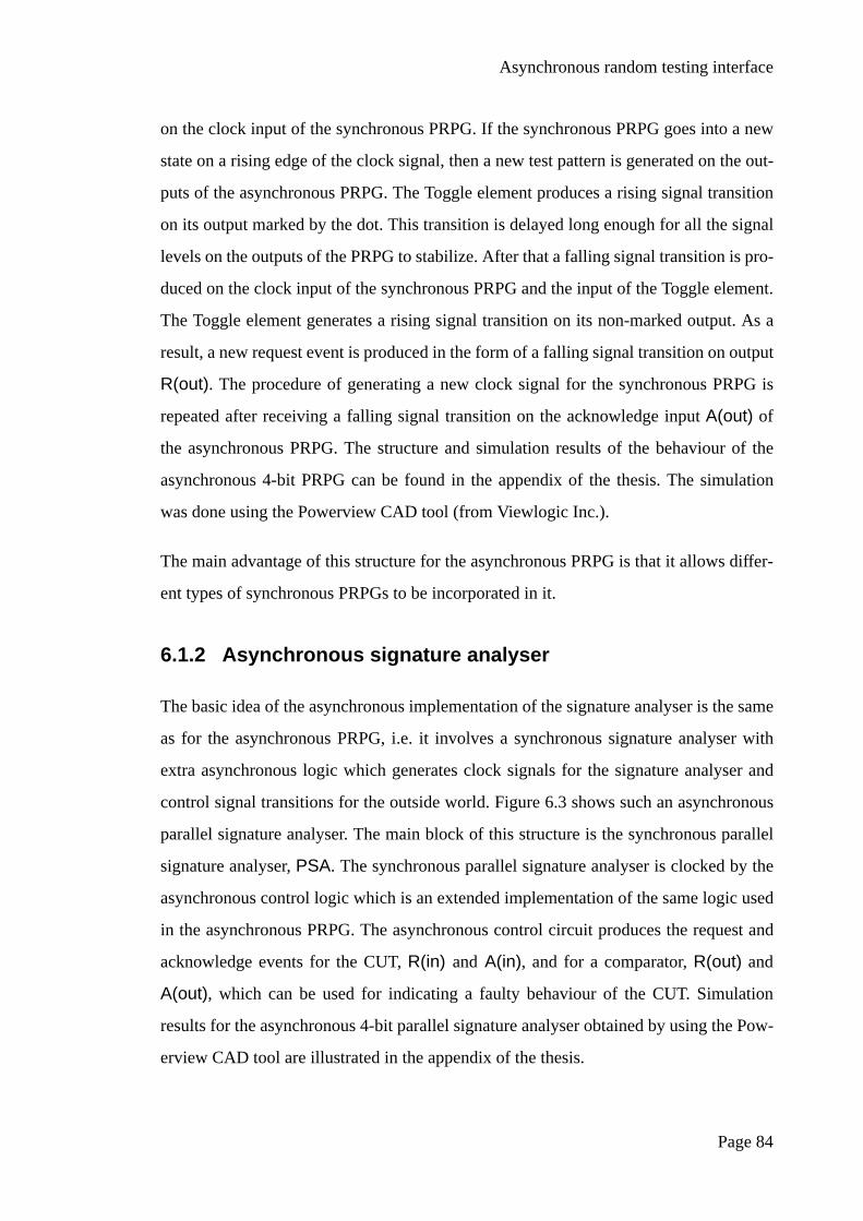
Asynchronous random testing interface
Page 84
on the clock input of the synchronous PRPG. If the synchronous PRPG goes into a new
state on a rising edge of the clock signal, then a new test pattern is generated on the out-
puts of the asynchronous PRPG. The Toggle element produces a rising signal transition
on its output marked by the dot. This transition is delayed long enough for all the signal
levels on the outputs of the PRPG to stabilize. After that a falling signal transition is pro-
duced on the clock input of the synchronous PRPG and the input of the Toggle element.
The Toggle element generates a rising signal transition on its non-marked output. As a
result, a new request event is produced in the form of a falling signal transition on output
R(out). The procedure of generating a new clock signal for the synchronous PRPG is
repeated after receiving a falling signal transition on the acknowledge input A(out) of
the asynchronous PRPG. The structure and simulation results of the behaviour of the
asynchronous 4-bit PRPG can be found in the appendix of the thesis. The simulation
was done using the Powerview CAD tool (from Viewlogic Inc.).
The main advantage of this structure for the asynchronous PRPG is that it allows differ-
ent types of synchronous PRPGs to be incorporated in it.
6.1.2 Asynchronous signature analyser
The basic idea of the asynchronous implementation of the signature analyser is the same
as for the asynchronous PRPG, i.e. it involves a synchronous signature analyser with
extra asynchronous logic which generates clock signals for the signature analyser and
control signal transitions for the outside world. Figure 6.3 shows such an asynchronous
parallel signature analyser. The main block of this structure is the synchronous parallel
signature analyser, PSA. The synchronous parallel signature analyser is clocked by the
asynchronous control logic which is an extended implementation of the same logic used
in the asynchronous PRPG. The asynchronous control circuit produces the request and
acknowledge events for the CUT, R(in) and A(in), and for a comparator, R(out) and
A(out), which can be used for indicating a faulty behaviour of the CUT. Simulation
results for the asynchronous 4-bit parallel signature analyser obtained by using the Pow-
erview CAD tool are illustrated in the appendix of the thesis.
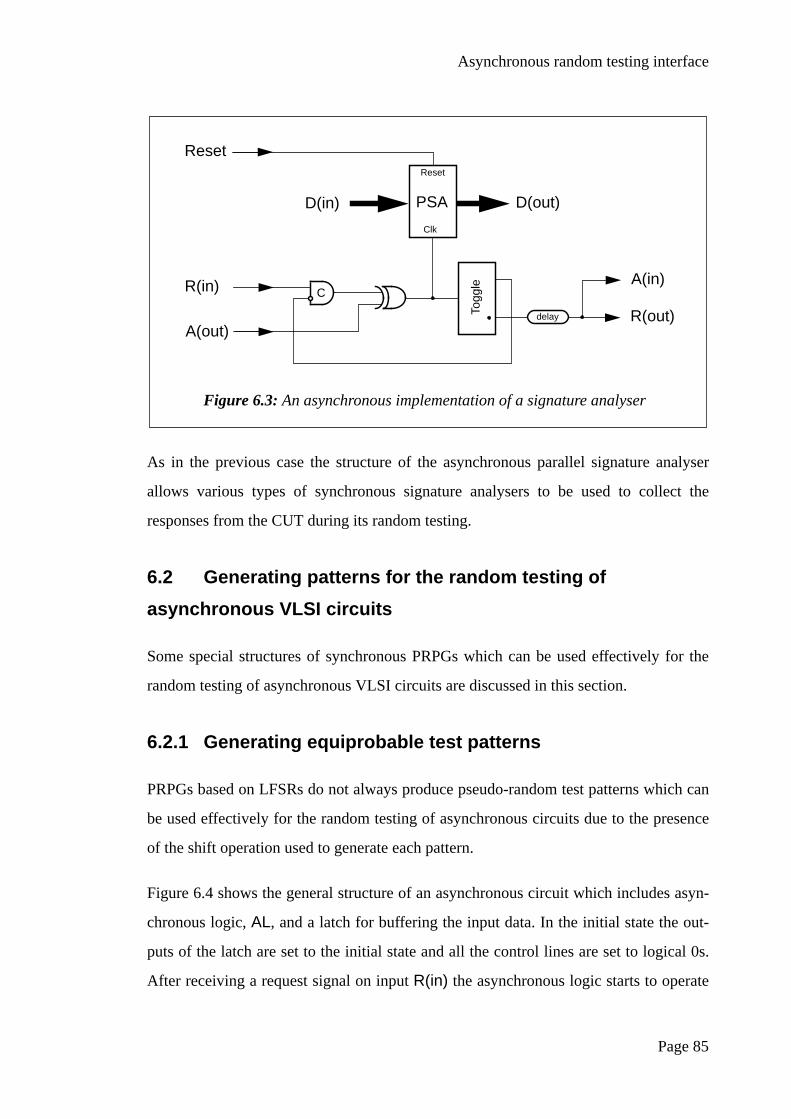
Asynchronous random testing interface
Page 85
As in the previous case the structure of the asynchronous parallel signature analyser
allows various types of synchronous signature analysers to be used to collect the
responses from the CUT during its random testing.
6.2 Generating patterns for the random testing of
asynchronous VLSI circuits
Some special structures of synchronous PRPGs which can be used effectively for the
random testing of asynchronous VLSI circuits are discussed in this section.
6.2.1 Generating equiprobable test patterns
PRPGs based on LFSRs do not always produce pseudo-random test patterns which can
be used effectively for the random testing of asynchronous circuits due to the presence
of the shift operation used to generate each pattern.
Figure 6.4 shows the general structure of an asynchronous circuit which includes asyn-
chronous logic, AL, and a latch for buffering the input data. In the initial state the out-
puts of the latch are set to the initial state and all the control lines are set to logical 0s.
After receiving a request signal on input R(in) the asynchronous logic starts to operate
R(in)
R(out)
C
delay
A(in)
Togg
le
A(out)
Clk
Reset
PSA
Reset
D(in) D(out)
Figure 6.3: An asynchronous implementation of a signature analyser

Asynchronous random testing interface
Page 86
on the data from its inputs, D(in), and the outputs of the latch. When the operation is
completed the asynchronous logic generates a request signal on its output r(out). As a
result, a request event is produced on the output R(out) of the asynchronous circuit.
After receiving the acknowledge event on the input A(out) the data from the input bus
D(in) are stored in the latch and the circuit generates the acknowledge signal on its out-
put A(in). If a new request signal appears on input R(in) the data operation procedure is
reiterated.
An example of the asynchronous circuit described above with some faults is illustrated
in Figure 6.5. The control lines are omitted to simplify the structure.
Let be a stuck-at-0 fault, be a stuck-at-1 or stuck-at-0 fault and be a bridging
fault. These faults cannot be detected by random test patterns generated by LFSRs. Let
the synchronous 4-bit LFSR (see Figure 3.3) incorporated into the structure of an asyn-
chronous PRPG be a source of pseudo-random patterns. It is easy to check that in the
pseudo-random test sequence (see Table 3.1) applied to the inputs of the circuit there is
no test pattern which can force any of the faults to manifest itself. For instance, during
the test 1) fault is untestable since only logical zeros are generated on the output of
C
P Pd
CCd
Latch
AL
R(in)
A(in)
R(out)
A(out)
Figure 6.4: Asynchronous logic with a latch
r(in) r(out)
a(in) a(out)
D(in) D1(out)
D2(out)
f1 f2 f3
f1

Asynchronous random testing interface
Page 87
the XOR gate; 2) fault cannot be detected because the Muller-C element keeps its ini-
tial state unchanged (if the initial state of the Muller-C element is a logical 1(0), then
stuck-at-1(0) fault is undetectable); 3) the bridging fault cannot be forced to mani-
fest itself since only two input stimuli, 00 and 11, are generated on the inputs of the
Muller-C element. The cause which makes these faults untestable lies in the nature of
pseudo-random patterns generated by an LFSR which uses a shift register to produce the
test patterns.
Let us build a PRPG which generates pseudo-random patterns on the basis of linear
feedback but without the obvious shift operation. Table 6.1 shows the modification pro-
Table 6.1: State modifying table for the 4-bit LFSR
State 1 2 3 4
0
1
2
3
4
f2
C
C
P Pd
CCdLa
tch
Asynchronous logic
1
2
3
1
2
3D(in)
D1(out)
D2(out)
Figure 6.5: An example of asynchronous circuit with undetectable faults
f1
f2f3
f2 f3
Q1 Q2 Q3 Q4
Q3 Q4⊕ Q1 Q2 Q3
Q2 Q3⊕ Q3 Q4⊕ Q1 Q2
Q1 Q2⊕ Q2 Q3⊕ Q3 Q4⊕ Q1
Q1 Q3 Q4⊕ ⊕ Q1 Q2⊕ Q2 Q3⊕ Q3 Q4⊕

Asynchronous random testing interface
Page 88
cedure for the first four states of the 4-bit LFSR built using the derivation polynomial
= . The pseudo-random sequence generated by this LFSR is the
reverse sequence produced by the LFSR shown in Figure 3.3. It is possible to continue
Table 6.1 to obtain expressions for all the states of the LFSR within the period. All these
expressions (except the first one) determine the structures of PRPGs. For example, the
fifth row (state number 4) defines the structure of PRPG which is equivalent to the struc-
ture shown in Figure 3.3 with the exception that all the flip-flops of the register are T
flip-flops. Table 6.2 contains the state sequence for the PRPG built using T flip-flops and
the derivation polynomial . As seen from the table the state sequence generated
by the PRPG has the maximal period (15 clocks). There is no obvious shift operation in
the generation of a new pattern. As a result, if these pseudo-random patterns are applied
to the inputs of the asynchronous circuit shown in Figure 6.5, then all the faults,,
and , can manifest themselves during pseudo-random testing.
Let us answer the following question: “Is it possible to use any of the rows in the state
modifying table to obtain the PRPG of maximal length?” The answer to this question
can be found after a detailed examination of the state sequence shown in Figure 6.2.
Table 6.3 contains the results showing the equivalence between states of the three 4-bit
PRPGs: the first column contains the state numbers of the PRPG built using T flip-flops,
Table 6.2: State sequence for the four-bit PRPG built using the state modificationprocedure
State State
0 1 1 1 1 8 0 0 1 1
1 1 0 0 0 9 0 0 1 0
2 1 1 0 0 10 1 0 1 1
3 1 0 1 0 11 1 1 1 0
4 0 1 1 1 12 0 0 0 1
5 0 1 0 0 13 1 0 0 1
6 0 1 1 0 14 0 1 0 1
7 1 1 0 1 15 1 1 1 1
ϕr X( ) 1 X3 X4+ +
ϕr X( )
f1 f2
f3
Q1 Q2 Q3 Q4 Q1 Q2 Q3 Q4
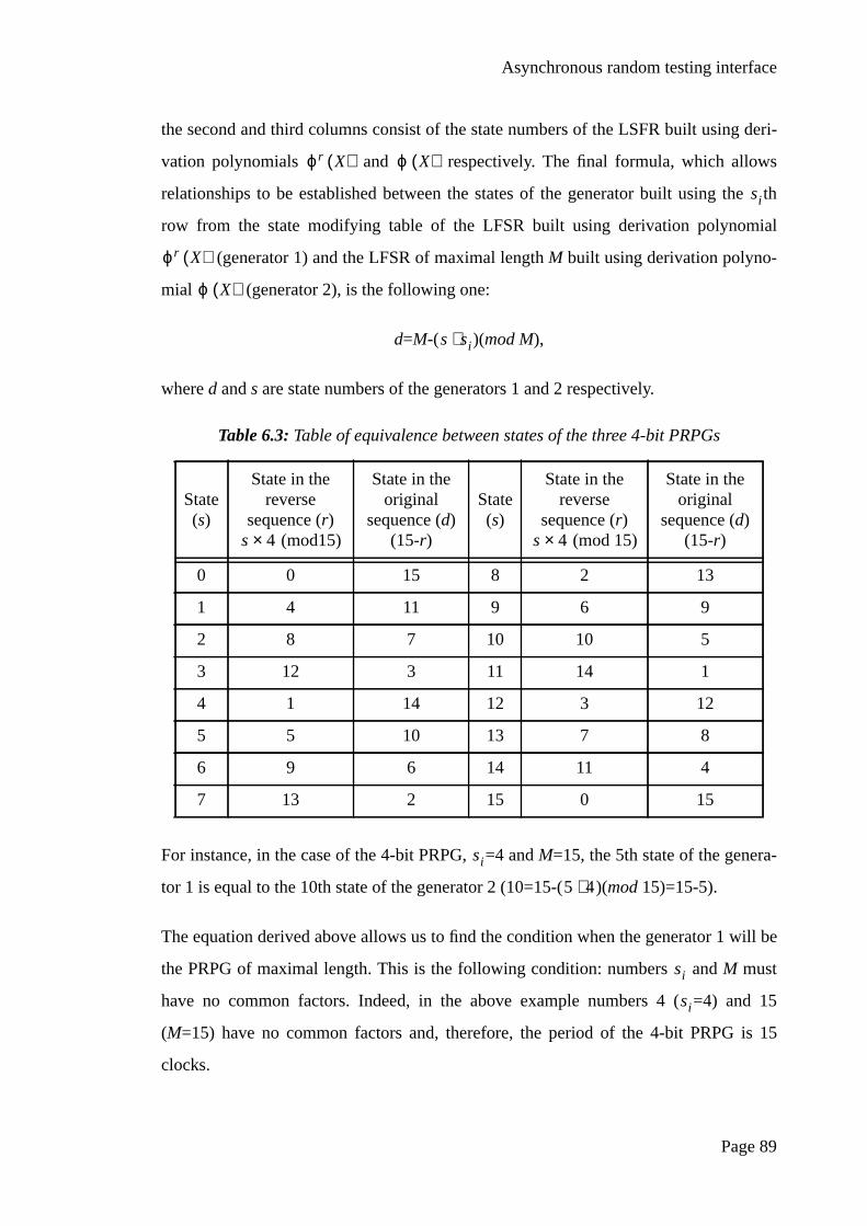
Asynchronous random testing interface
Page 89
the second and third columns consist of the state numbers of the LSFR built using deri-
vation polynomials and respectively. The final formula, which allows
relationships to be established between the states of the generator built using theth
row from the state modifying table of the LFSR built using derivation polynomial
(generator 1) and the LFSR of maximal lengthM built using derivation polyno-
mial (generator 2), is the following one:
d=M-( )(mod M),
where d ands are state numbers of the generators 1 and 2 respectively.
For instance, in the case of the 4-bit PRPG,=4 andM=15, the 5th state of the genera-
tor 1 is equal to the 10th state of the generator 2 (10=15-()(mod 15)=15-5).
The equation derived above allows us to find the condition when the generator 1 will be
the PRPG of maximal length. This is the following condition: numbers andM must
have no common factors. Indeed, in the above example numbers 4 (=4) and 15
(M=15) have no common factors and, therefore, the period of the 4-bit PRPG is 15
clocks.
Table 6.3: Table of equivalence between states of the three 4-bit PRPGs
State(s)
State in thereverse
sequence (r) (mod15)
State in theoriginal
sequence (d)(15-r)
State(s)
State in thereverse
sequence (r) (mod 15)
State in theoriginal
sequence (d)(15-r)
0 0 15 8 2 13
1 4 11 9 6 9
2 8 7 10 10 5
3 12 3 11 14 1
4 1 14 12 3 12
5 5 10 13 7 8
6 9 6 14 11 4
7 13 2 15 0 15
ϕr X( ) ϕ X( )
si
ϕr X( )
ϕ X( )
s si⋅
s 4× s 4×
si
5 4⋅
si
si

Asynchronous random testing interface
Page 90
Table 6.4 shows the state modification procedure for the first eight states of the 6-bit
LFSR built using the derivation polynomial = . As the period of the
6-bit LSFR is 63 clocks, it is possible to use the 9th row of Table 6.4 ( =8) as a rule for
modifying states of memory elements in order to obtain the 6-bit PRPG of maximal
length (the numbers 8 and 63 have no common factors). Figure 6.6 shows the structure
of this PRPG. The realization of such a 6-bit PRPG requires the use of more XOR gates
than the equivalent LFSR and cannot allow the use of T flip-flops to obtain a simpler
structure.
Table 6.4: State modifying table for the 6-bit LFSRS
tate
1 2 3 4 5 6
0
1
2
3
4
5
6
7
8
Q1 Q2 Q3 Q4 Q5 Q6
Q5 Q6⊕ Q1 Q2 Q3 Q4 Q5
Q4 Q5⊕ Q5 Q6⊕ Q1 Q2 Q3 Q4
Q3 Q4⊕ Q4 Q5⊕ Q5 Q6⊕ Q1 Q2 Q3
Q2 Q3⊕ Q3 Q4⊕ Q4 Q5⊕ Q5 Q6⊕ Q1 Q2
Q1 Q2⊕ Q2 Q3⊕ Q3 Q4⊕ Q4 Q5⊕ Q5 Q6⊕ Q1
Q1 Q5 Q6⊕ ⊕ Q1 Q2⊕ Q2 Q3⊕ Q3 Q4⊕ Q4 Q5⊕ Q5 Q6⊕
Q4 Q6⊕ Q1 Q5 Q6⊕ ⊕ Q1 Q2⊕ Q2 Q3⊕ Q3 Q4⊕ Q4 Q5⊕
Q3 Q5⊕ Q4 Q6⊕ Q1 Q5 Q6⊕ ⊕ Q1 Q2⊕ Q2 Q3⊕ Q3 Q4⊕
ϕr X( ) 1 X5 X6+ +
si
D D D D D D
1 2 3 4 5 6
Figure 6.6: The 6-bit PRPG based on using the 8-th state from the statemodification table of the 6-bit LSFR

Asynchronous random testing interface
Page 91
Thus, the implementation complexity of a PRPG to produce pseudo-random patterns
without the obvious shift operation depends on:
• the number of outputs of the PRPG;
• the complexity of the derivation polynomial.
The technique for building PRPGs proposed in this section allows the creation of new
structures for PRPGs which can be widely used for the pseudo-random (random) testing
of various types of asynchronous VLSI circuits.
6.2.2 A PRPG for weighted test patterns
It was already noted that the derivation of tests from a source of equiprobable patterns to
test data paths of digital circuits is not always an efficient procedure in terms of time and
fault coverage [52-55]. The Monte Carlo method for logic testing of digital circuits has
been proposed [53]. It was shown that in combinational logic the probability of detect-
ing a stuck-at fault can be optimized by a proper selection of the probabilities of a zero
and one on the outputs of the source of random test patterns. This fact was used for
improving the efficiency of test generation over the commonly employed heuristics of
equiprobable 0 and 1.
PRPG
CLf
1
M
j
m+1m+2
m+i
Figure 6.7: A general structure of a PRPG with given signal probabilities on itsoutputs

Asynchronous random testing interface
Page 92
Figure 6.7 shows a general structure of a weighted pseudo-random pattern generator
(WPRPG) which generates pseudo-random signals with a given probability of a one
(zero) on its output . In this structure the combinational logic, CL, is fed with a subset
of the outputs of the PRPG which is the source of equiprobable patterns. The probability
of a one and zero on the output of the combinational logic can be estimated as
and ,
where ( ) is the number of ones (zeros) in the truth table of Boolean function.
Thus, the basic procedure for deriving the desired signal probability on the outputs of
the WPRPG can be described by the following sequence of steps:
• put the desired number of ones (zeros) in the truth table of the Boolean function;
• make the minimal (in terms of logic elements) realization of the function.
The second step is important for obtaining a fast version of the WPRPG.
6.3 Program tools for the behavioural simulation of PRPGs
In order to have program tools for the simulation of the pseudo-random (random) testing
of asynchronous VLSI circuits a behavioural model of the universal PRPG was
designed. This simulation program for the universal PRPG is written in the C language.
It includes three main programs (see Figure 6.8):
• long_gps.c which generates equiprobable pseudo-random patterns;
• rom_prob.c simulates the behaviour of the WPRPG based on using ROMs;
• prpg_prob.c which is a simulation program for the WPRPG based on using addi-
tional logic elements.
The key features of these programs are the following:
Long_gps.c generates:
fj
p fj( ) N1 2 i−⋅= q fj( ) N0 2 i−⋅=
N1 N0 fj
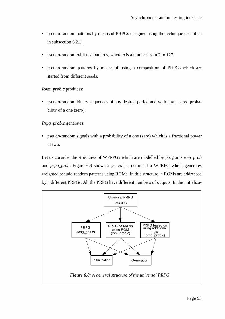
Asynchronous random testing interface
Page 93
• pseudo-random patterns by means of PRPGs designed using the technique described
in subsection 6.2.1;
• pseudo-randomn-bit test patterns, wheren is a number from 2 to 127;
• pseudo-random patterns by means of using a composition of PRPGs which are
started from different seeds.
Rom_prob.c produces:
• pseudo-random binary sequences of any desired period and with any desired proba-
bility of a one (zero).
Prpg_prob.c generates:
• pseudo-random signals with a probability of a one (zero) which is a fractional power
of two.
Let us consider the structures of WPRPGs which are modelled by programsrom_prob
and prpg_prob. Figure 6.9shows a general structure of a WPRPG which generates
weighted pseudo-random patterns using ROMs. In this structure,n ROMs are addressed
by n different PRPGs. All the PRPG have different numbers of outputs. In the initializa-
Universal PRPG
(gtest.c)
PRPG(long_gps.c)
PRPG based onusing additional
logic(prpg_prob.c)
PRPG based onusing ROM
(rom_prob.c)
Initialization Generation
Figure 6.8: A general structure of the universal PRPG
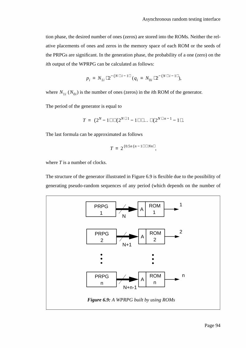
Asynchronous random testing interface
Page 94
tion phase, the desired number of ones (zeros) are stored into the ROMs. Neither the rel-
ative placements of ones and zeros in the memory space of each ROM or the seeds of
the PRPGs are significant. In the generation phase, the probability of a one (zero) on the
ith output of the WPRPG can be calculated as follows:
( ),
where ( ) is the number of ones (zeros) in theith ROM of the generator.
The period of the generator is equal to
.
The last formula can be approximated as follows
,
whereT is a number of clocks.
The structure of the generator illustrated in Figure 6.9 is flexible due to the possibility of
generating pseudo-random sequences of any period (which depends on the number of
pi N1i 2 N i 1−+( )−⋅= qi N0i 2 N i 1−+( )−⋅=
N1i N0i
T 2N 1−( ) 2N 1+ 1−( ) … 2N n 1−+ 1−( )⋅ ⋅ ⋅=
T 2 0.5n n 1−( ) Nn+( )=
ROMPRPG1 1
A
ROMPRPG2 2
A
ROMPRPGn n
A
N
N+1
N+n-1
1
2
n
Figure 6.9: A WPRPG built by using ROMs
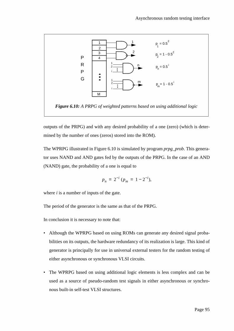
Asynchronous random testing interface
Page 95
outputs of the PRPG) and with any desired probability of a one (zero) (which is deter-
mined by the number of ones (zeros) stored into the ROM).
The WPRPG illustrated in Figure 6.10 is simulated by programprpg_prob. This genera-
tor uses NAND and AND gates fed by the outputs of the PRPG. In the case of an AND
(NAND) gate, the probability of a one is equal to
( ),
wherei is a number of inputs of the gate.
The period of the generator is the same as that of the PRPG.
In conclusion it is necessary to note that:
• Although the WPRPG based on using ROMs can generate any desired signal proba-
bilities on its outputs, the hardware redundancy of its realization is large. This kind of
generator is principally for use in universal external testers for the random testing of
either asynchronous or synchronous VLSI circuits.
• The WPRPG based on using additional logic elements is less complex and can be
used as a source of pseudo-random test signals in either asynchronous or synchro-
nous built-in self-test VLSI structures.
pn 2 i−= pm 1 2 i−−=
1
234
M
1
2
n
m
P
R
P
G
12
i
12
i
p = 0.5
p = 0.5
p = 1 - 0.5
p = 1 - 0.5
2
2
i
i
1
2
n
m
Figure 6.10: A PRPG of weighted patterns based on using additional logic

Page 96
Chapter 7 : Test lengths for
random testing of
micropipelines
There are two important characteristics of random testing: the time taken to generate the
desired set of test vectors, and the probability of detecting all possible faults from the
predetermined class of the circuit’s faults. The first parameter reflects the practical usa-
bility of the test set or simply the random pattern testability of the circuit under test. The
second parameter is a characteristic of the quality of random testing.
Figure 7.1 shows a general structure for the random testing of a micropipeline all the
latches of which are in the pass mode during the test. The primary inputs of the combi-
national logic, CL, are supplied with test patterns which are generated by the PRPG
asynchronously. The responses from the primary outputs of the combinational logic are
collected by the parallel signature analyser, PSA. The total test time of the micropipeline
depends on the time for the random testing of the combinational logic, which basically
consists of a number of subcircuits ( ). It is assumed that the number of
outputs of the PRPG is larger than the number of inputs of the combinational circuit
under test. This can be justified because usually random test equipment is universal and
uses PRPGs which produce very long pseudo-random sequences. The question is, how
is it possible to estimate the test length for the random testing of such a combinational
network?
Past work has already addressed the question of determining the pseudo-random and
random pattern test lengths [25, 56-58]. In some of these papers mathematical expres-
sions are derived for the test length on the basis of the smallest detection probability of
possible faults in the circuit [25, 56]. On the other hand, it was shown by J. Savir and P.
H. Bardell [57] that the random pattern test length increases logarithmically with the
number of faults which have a detection probability close to the minimum. The main
CLi 1 i w≤ ≤
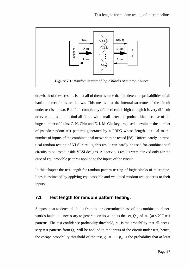
Test lengths for random testing of micropipelines
Page 97
drawback of these results is that all of them assume that the detection probabilities of all
hard-to-detect faults are known. This means that the internal structure of the circuit
under test is known. But if the complexity of the circuit is high enough it is very difficult
or even impossible to find all faults with small detection probabilities because of the
huge number of faults. C. K. Chin and E. J. McCluskey proposed to evaluate the number
of pseudo-random test patterns generated by a PRPG whose length is equal to the
number of inputs of the combinational network to be tested [58]. Unfortunately, in prac-
tical random testing of VLSI circuits, this result can hardly be used for combinational
circuits to be tested inside VLSI designs. All previous results were derived only for the
case of equiprobable patterns applied to the inputs of the circuit.
In this chapter the test length for random pattern testing of logic blocks of micropipe-
lines is estimated by applying equiprobable and weighted random test patterns to their
inputs.
7.1 Test length for random pattern testing.
Suppose that to detect all faults from the predetermined class of the combinational net-
work’s faults it is necessary to generate on its inputs the set, , of test
patterns. The test confidence probability threshold,, is the probability that all neces-
sary test patterns from will be applied to the inputs of the circuit under test, hence,
the escape probability threshold of the test, , is the probability that at least
CL
CL1
CL2
CLw
Figure 7.1: Random testing of logic blocks of micropipelines
PSA
PRPG
R(in)
A(in)
R(out)
A(out)
D(in) D(out)
n Qm m m 2n≤( )
pt
Qm
qt 1 pt−=

Test lengths for random testing of micropipelines
Page 98
one pattern from the set will not be applied to the inputs of the combinational logic
during the test. The test length, , is the total number of test patterns applied to the
inputs of the circuit.
Figure 7.2 shows the basic structure for pseudo-random testing an-input combina-
tional circuit. It assumes that the number of inputs to the combinational logic is fewer
than the total number of storage elements of the PRPG. In this case it is possible to con-
sider the pseudo-random test procedure as the random testing of the combinational logic
by means of applying equiprobable test patterns to its inputs [58]. The probability that
any one pattern will be generated on outputs of the PRPG is . During the ran-
dom pattern testing of the combinational circuit the test results are observed in a com-
pact form on the outputs of a signature analyser.
Let us estimate the random test length that is sufficient that different -bit
test patterns to appear on the circuit’s inputs. Consider the event when fewer than
of the required test vectors are generated on the inputs during the random test of length
. The event is the union of the following events: the event when pattern
does not appear on the inputs; the event when pattern does
not appear, and so on up to event when pattern does not appear. The
Qm
Tm
n
n p 2 n−=
12
j+1j+2
j+n
N
p1p2
pn
CL
To SA
PRPG
Figure 7.2: Random testing a combinational logic block.
m m 2n≤( ) n
Em m
Tm Em m A1 r1
r1 Qm∈( ) A2 r2 r2 Qm∈( )
Am rm rm Qm∈( )

Test lengths for random testing of micropipelines
Page 99
events included in are not mutually exclusive, therefore the equation for the proba-
bility of , , can be obtained with the help of a Venn Diagram [59]
(5)
As the probability is the escape probability of the test pattern, taking into
account the independent character of the test patterns which are used, the equation for
the probability can be written as , ( ).
Using the Venn Diagram it is possible to modify equation (5) into an inequality, i.e.
. (6)
The probability should be no larger than the escape probability threshold, that is
. It follows from (6) that the inequality suffices to ensure
that all test vectors will appear on the inputs with no less than the predetermined test
confidence probability. Thus, the lower bound of the test length of the random test pro-
cedure, , can be estimated as
. (7)
It is known [60] that if (i.e. the probability of generating one defined n-bit pattern
is very close to zero) then . Hence, if the number of inputs to the com-
binational network under test is large enough then inequality (7) will take the following
form
. (8)
Expression (8) can be derived from the Poisson theorem [60] because in the case when
( ) and the mathematical expectation of the number of
appearances of one random pattern,, during the test, is going to be a constant, i.e.
Em
Em p Em( )
p Em( ) p Ai( )i 1=
m
i j≠( )
∑ p Ai( ) p Aj( ) … 1−( ) m 1+ p A1( ) p A2( ) …p Am( )+ +⋅i j, 1=
m
∑−=
p Ai( ) ri
p Ai( ) p Ai( ) 1 p−( ) Tm= 1 i m≤ ≤
p Em A1 A2 … Am∪ ∪ ∪=( ) p Ai( )i 1=
m
∑≤ m 1 p−( ) Tm⋅=
p Em( )
p Em( ) qt≤ m 1 p−( ) Tm⋅ qt≤
m
Tm
Tm
qt m⁄( )log
1 p−( )log≥
p 0→
1 p−( )log p−→
Tm 2n m qt⁄( )log≥
p 0→ p const= Tm ∞→
a

Test lengths for random testing of micropipelines
Page 100
. Therefore the probability, , that during the random test of
length the number of appearances of one pattern will be equal to is the Poisson
probability with parameters and :
, where .
The probability ( ) that only one pattern will not come out after the ran-
dom test is the Poisson probability with :
.
Taking into account that and (6) the expression (8) for the lower bound of
the random pattern test length can be obtained.
To estimate the actual numerical values of the variable which allows formula (8) to be
used instead of (7) without losing significant accuracy it is reasonable to evaluate the
relative error, , of the random pattern test lengths calculated by using formula (8):
, (9)
where and are calculated from (7) and (8) respectively.
Substituting the corresponding expressions for and in inequality (9) the follow-
ing inequality is obtained:
.
As the inequality for can be rewritten using a limit, i.e.
.
It is known that . Therefore, the final inequality for the
relative error can be written in the following form: . From this formula
it is possible to find the inequality for taking into account that , i.e.
a Tm p const→⋅= P a k,( )
Tm k
a k
P a k,( ) e a− ak k!⁄→ k 0 1 2 …, , ,=
p Ai( ) i 1 m,=
k 0=
p Ai( ) P a 0,( ) eTm
p−= =
p Em( ) qt≤
n
ε
Tm″ Tm−( ) Tm⁄ ε≤
Tm Tm″
Tm Tm″
1 p−( )logp
− 1− ε≤
p 0→ ε
1 p−( )logpp 0→
lim− 1− ε≤
1 p−( )logp−p 0→
lim 1 p−( ) 1−=
ε 1 p−( ) 1− ε≤
n p 2 n−=
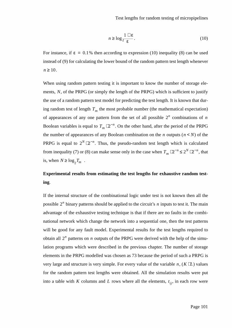
Test lengths for random testing of micropipelines
Page 101
. (10)
For instance, if % then according to expression (10) inequality (8) can be used
instead of (9) for calculating the lower bound of the random pattern test length whenever
.
When using random pattern testing it is important to know the number of storage ele-
ments, , of the PRPG (or simply the length of the PRPG) which is sufficient to justify
the use of a random pattern test model for predicting the test length. It is known that dur-
ing random test of length the most probable number (the mathematical expectation)
of appearances of any one pattern from the set of all possible combinations of
Boolean variables is equal to . On the other hand, after the period of the PRPG
the number of appearances of any Boolean combination on the outputs ( ) of the
PRPG is equal to . Thus, the pseudo-random test length which is calculated
from inequality (7) or (8) can make sense only in the case when , that
is, when .
Experimental results from estimating the test lengths for exhaustive random test-
ing.
If the internal structure of the combinational logic under test is not known then all the
possible binary patterns should be applied to the circuit’s inputs to test it. The main
advantage of the exhaustive testing technique is that if there are no faults in the combi-
national network which change the network into a sequential one, then the test patterns
will be good for any fault model. Experimental results for the test lengths required to
obtain all patterns on outputs of the PRPG were derived with the help of the simu-
lation programs which were described in the previous chapter. The number of storage
elements in the PRPG modelled was chosen as 73 because the period of such a PRPG is
very large and structure is very simple. For every value of the variable, ( ) values
for the random pattern test lengths were obtained. All the simulation results were put
into a table with columns and rows where all the elements,, in each row were
n1 ε+
ε2log≥
ε 0.1=
n 10≥
N
Tm
2n n
Tm 2 n−⋅
n n N<
2N 2 n−⋅
Tm 2 n−⋅ 2N 2 n−⋅≤
N Tm2log≥
2n n
2n n
n K L⋅
K L tij
Test lengths for random testing of micropipelines
Page 102
sorted into increasing order, i.e. , . The final result was
obtained in the form of vector with elements where
, .
Each element of the vector is a value for the statistical random test length with test
confidence probability , where . The last element of the vector
( ) has no meaning because in practice it is impossible to achieve absolute confi-
dence in a random testing. In the simulation experiments the number of columns and
rows were equal to 100, i.e. and . Apparently, the larger is the
more precisely the value of the random test lengths can be calculated, that is the statisti-
Table 7.1: Statistical and theoretical random lengths for the exhaustive testing ofcombinational networks
(7) (8)
2 0.9 13 13 14
0.95 15 15 17
0.99 20 21 23
4 0.9 78 79 81
0.95 89 89 92
0.99 109 114 118
8 0.9 1965 2005 2009
0.95 2134 2182 2186
0.99 2500 2593 2598
10 0.9 9336 9451 9455
0.95 10012 10160 10165
0.99 11279 11808 11813
12 0.9 42978 43485 43500
0.95 45727 46323 46340
0.99 51148 52913 52932
ti1 ti2 … tiK≤ ≤ ≤ 1 i L≤ ≤
K
tj1L
tiji 1=
L
∑= 1 j K≤ ≤
tj T2n
pt j K⁄= 1 j K 1−≤ ≤
j K=
K 100= L 100= L
n pt T2n
T2n
Test lengths for random testing of micropipelines
Page 103
cal random pattern test length will be closer to the theoretical value. The values of,
and chosen in the simulation were restricted by the available simulation time on the
computers used for the experiment.
Some of the practical and theoretical estimates of the random test length are shown in
Table 7.1. The column headed contains the values of the test lengths calculated by
using formulas (7) and (8). Statistical test lengths are placed in the column headed.
In order to restrict the table size the results are presented only for=0.9, 0.95, 0.99, and
=2, 4, 8, 10 and 12. It can be seen from Table 7.1 that the simulation results are no
larger than the theoretically obtained ones. This confirms that expressions (7) and (8)
may be used to calculate the lower bound of the random test length. Formula (8) is less
complex than (7) and in fact it can be used instead of (7).
7.2 Test length for random testing using weighted patterns
Random testing using only equiprobable random test patterns is not always the optimal
test procedure for obtaining the minimal (or close to minimal) random pattern test length
for a certain subset of test patterns from the set of all possible binary combinations. To
reduce the length of random pattern testing, methods were derived for achieving optimal
output signal probabilities for generators of weighted pseudo-random patterns
(WPRPG) [54-55]. The aim of this section is to present an approach for estimating the
random pattern test length, , which will guarantee the test confidence probability, ,
of obtaining the desired number, , of weighted test patterns from the set. In general
the source of random test patterns can be a WPRPG with different signal probabilities
on its outputs. Let us calculate the minimal probability, , of a random pattern from
the set ,
i.e. , , ,
where ,
Suppose that all test patterns from the set have the same probability of appearance
which is equal to . Thus, the weighted random testing of a combinational logic cir-
K L
n
T2n
T2n
pt
n
Tm pt
m Qm
pmin
Qm
αi∀ 0 1,{ }∈ 1 i n≤ ≤( ) pmin MIN p1α1 p2
α2… pnαn⋅( )=
α1α2…αn( ) Qm∈ piαi
pi, if αi 1,=1 pi− , if αi 0.=
=
m Qm
pmin

Test lengths for random testing of micropipelines
Page 104
cuit can be substituted on the random pattern testing by means of equiprobable test vec-
tors. In this case for estimating the random pattern test length it is possible to use
expression (8) where , i.e.
. (11)
Obviously inequality (11) evaluates the redundant lower bound for the test length for the
random testing with the help of the WPRPG.
Consider the case when the set contains only two test patterns with probabilities of
appearance and respectively. The model of the generation of all these patterns
during random testing can be represented by the Markov chain (Figure 7.3) with four
states: and are the states which correspond to the appearance of neither and both
test patterns respectively; states and correspond to the appearance of the first and
the second test pattern respectively. The transition probabilities between the states are
marked on the transition arcs of the Markov chain. The initial state probabilities of the
Markov chain are , .
p pmin=
TmU pmin
1− m qt⁄( )log≥
Qm
v1 v2
S0 S12
S1 S2
P0 S0( ) 1= P0 S1( ) P0 S2( ) P0 S12( ) 0= = =
S1
S2
S0
v1
1 v1−
v2
1 v2−
1 v1− v2−1
v2 v1
S12
Figure 7.3: The Markov chain describing the process of the appearance of twodifferent random patterns

Test lengths for random testing of micropipelines
Page 105
Let us estimate the probability that during the generation of test patterns by
the WPRPG the patterns from set will appear. For this purpose the system of differ-
ence equations which describes the behaviour of the Markov chain (Figure 7.3) can be
composed as:
.
The solution of this system of difference equations subject to the initial conditions is
given by
.
According to the condition of random pattern testing the probability should be
no less than the test confidence probability, hence,
. (12)
Inequality (12) can be simplified taking into account that is a positive
value which is less than either or , i.e.
. (13)
Suppose that , where , . It follows from expression (13) that
the larger parameter is, the less effect probability has on the random pattern test
length. In practice the random testing of-input digital circuits presumes that the prob-
Pk S12( ) k
Q2
Pk S0( ) 1 v1 v2−−( ) Pk 1− S0( ) ,⋅=
Pk S1( ) 1 v2−( ) Pk 1− S1( )⋅ v1 Pk 1− S0( ) ,⋅+=
Pk S2( ) 1 v1−( ) Pk 1− S2( )⋅ v2 Pk 1− S0( ) ,⋅+=
Pk S12( ) v2 Pk 1− S1( )⋅ v1 Pk 1− S2( )⋅ Pk 1− S12( )+ +=
Pk S0( ) 1 v1 v2+( )−( ) k;= Pk S1( ) 1 v2−( ) k 1 v1 v2+( )−( ) k;−=
Pk S2( ) 1 v1−( ) k 1 v1 v2+( )−( ) k;−=
Pk S12( ) 1 1 v1−( ) k 1 v2−( ) k−−= 1 v1 v2+( )−( ) k+
Pk S12( )
pt
1 1 v1−( ) k 1 v2−( ) k− 1 v1 v2+( )−( ) k+− pt≥
1 v1 v2+( )−( ) k
1 v1−( ) k 1 v2−( ) k
1 v1−( ) k 1 v2−( ) k+ qt≤
v2 cv1= c const= c 1≥
c v2
n
Test lengths for random testing of micropipelines
Page 106
abilities of appearance of rare test patterns are very small (especially if is large
enough) and . Therefore, expression (13) can be approximated as
. (14)
Let us estimate the value of parameter that will change the test length,, calculated
from formula (14) by no more than the predetermined value of a relative error, . In
other words, it is required to find from the following inequality:
, (15)
where is the test length calculated from (10) when .
Let , hence, inequality (14) can be rewritten as
. (16)
If then the solution of inequality (16) is obvious: , that is,
. When the solution of quadratic inequality (16) is the follow-
ing: (the second root of quadratic equation (16) is negative
whereas ), therefore, . Substituting and in
(15) the following inequality is derived:
. (17)
When it is necessary to solve the cubic inequality (16). Cubic equation (16) has
three roots: one is real; the other two are complex conjugate roots [60]. As should be a
positive real value then the solution of cubic inequality (16) can be found as
, where , therefore,
. Substituting the expression for in (15)
the following inequality is obtained:
n
k ∞→
ev1k−
ec− v1k+ qt≤
c k
ε
c
k1 kc−k1
ε≤
k1 c 1=
x ev− 1k=
xc x qt−+ 0≤
c 1= x qt 2⁄≤
k1 v11− 2 qt⁄( )log≥ c 2=
x 1 4qt+ 1−( ) 2⁄≤
x 0≥ k2 v11− 2 1 4qt+ 1−( )⁄( )log≥ k1 k2
1 4qt+ 1−( ) qt⁄( )log
2 qt⁄( )logε≤
c 3=
x
x D q+ t 2⁄3 D qt 2⁄−3−≤ D 1 27⁄ qt2 4⁄+=
k3 v11−
D q+ t 2⁄3 D qt 2⁄−3−1−
log≥ k3

Test lengths for random testing of micropipelines
Page 107
. (18)
Table 7.2 shows the results of numerical solutions of equation (15), i.e. ,
for and different values of variable . The columns marked as and
represent the solutions of equations (17) and (18) respectively.
Table 7.2: Numerical solutions of inequalities (17) and (18)
Figure 7.4 shows a graph of the dependence of the relative error on the escape proba-
bility for . It can be seen that the solutions of inequalities (17) and (18) lie
beneath the appropriate curves and . From Table 7.2
and Figure 7.4 it can be seen that values and are very close together
for high confidence random pattern testing. Thus, choosing a value of variable which
is more than 2 does not significantly affect the random test length with the high test con-
fidence probability. In other words, if the probability of one test pattern is more than
twice the minimal probability of a test pattern from set then to estimate the lower
bound for the random pattern test length it is sufficient to take into account the probabil-
ities of test patterns which belong to the range [ ]. Therefore, the final algo-
rithm for calculating the lower bound for the test length for random testing by means of
applying weighted test patterns can be described as the following sequence of steps:
0.001 9.1% 9.1%
0.01 12.9% 13.1%
0.05 17.5% 18.7%
0.1 20.2% 22.8%
0.2 23.3% 28.5%
0.3 25.1% 32.6%
0.5 27.5% 38.1%
D q+ t 2⁄3 D qt 2⁄−3−( ) 2qt
( )log
2 qt⁄( )logε≤
ε ε c qt,( )=
c 2 3,= qt ε 2 qt,( )
ε 3 qt,( )
qt ε 2 qt,( ) ε 3 qt,( )
ε
qt c 2 3,=
ε 2 qt,( ) ε 3 qt,( ) ε 4 qt,( ) …≤≤≤
ε 2 qt,( ) ε 3 qt,( )
c
Qm
pmin 2pmin,
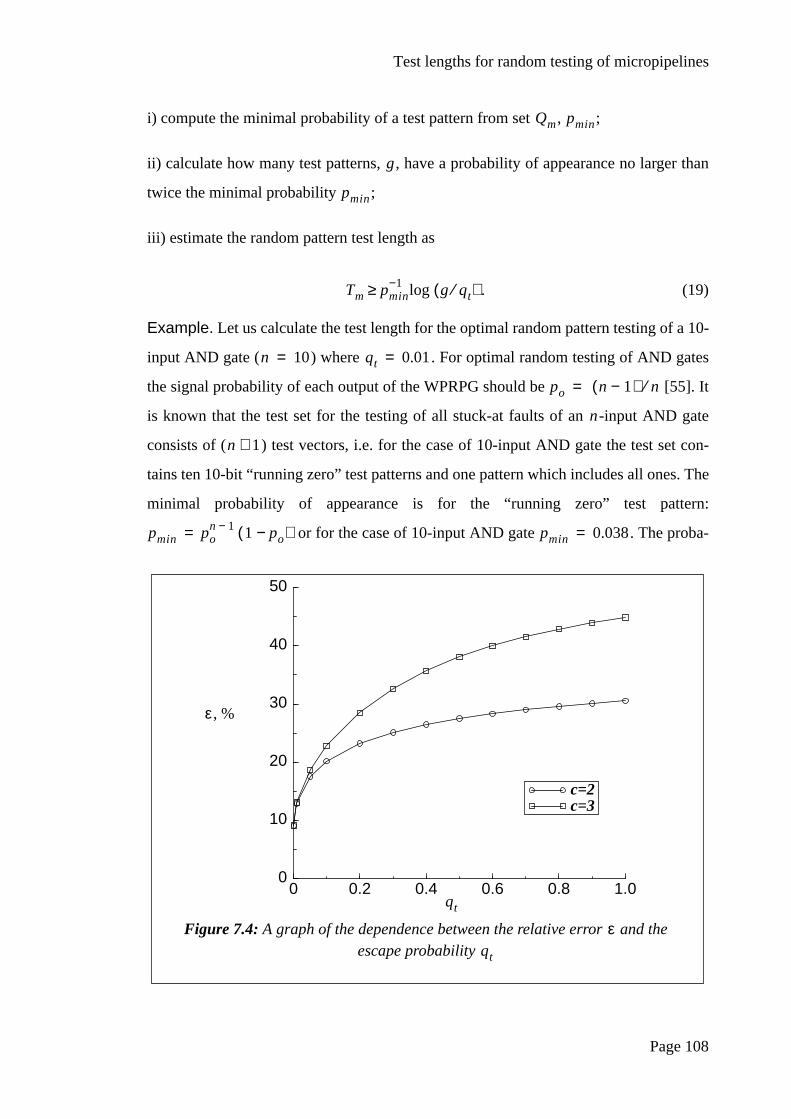
Test lengths for random testing of micropipelines
Page 108
i) compute the minimal probability of a test pattern from set, ;
ii) calculate how many test patterns,, have a probability of appearance no larger than
twice the minimal probability ;
iii) estimate the random pattern test length as
. (19)
Example. Let us calculate the test length for the optimal random pattern testing of a 10-
input AND gate ( ) where . For optimal random testing of AND gates
the signal probability of each output of the WPRPG should be [55]. It
is known that the test set for the testing of all stuck-at faults of an-input AND gate
consists of ( ) test vectors, i.e. for the case of 10-input AND gate the test set con-
tains ten 10-bit “running zero” test patterns and one pattern which includes all ones. The
minimal probability of appearance is for the “running zero” test pattern:
or for the case of 10-input AND gate . The proba-
Qm pmin
g
pmin
Tm pmin1− g qt⁄( )log≥
n 10= qt 0.01=
po n 1−( ) n⁄=
n
n 1+
pmin pon 1− 1 po−( )= pmin 0.038=
0 0.2 0.4 0.6 0.8 1.00
10
20
30
40
50
c=2c=3
qt
, %ε
Figure 7.4: A graph of the dependence between the relative error and theescape probability
εqt

Test lengths for random testing of micropipelines
Page 109
bility, , that “all ones” test vector will appear is. As , . The
probability is much more than two times larger probability , therefore, .
To calculate the test length for the optimal random pattern testing of a 10-input AND
gate expression (19) is used, i.e. . In comparison with random testing using
equiprobable random test patterns ( ) the random pattern test length is
reduced by a factor greater than 40.
Table 7.3 contains some experimental and theoretical results for evaluating test lengths
for the exhaustive random testing of a 3-input combinational circuit. The test lengths
calculated from expression (19) are shown in the column headed. The simulation
results are in the column . Table 7.3 confirms that formula (19) can be used in prac-
tice for predicting the number of weighted random test patterns needed for the testing of
a combinational circuit.
Table 7.3: Theoretical and experimental results for estimating the test lengths forrandom pattern testing of a 3-input combinational circuit
0.125 0.25 0.5 0.016 20.9 192 183
0.99 339 310
0.1 0.25 0.5 0.013 20.9 240 231
0.99 424 396
0.125 0.125 0.25 0.003 10.9 590 588
0.99 1179 1083
0.25 0.333 0.5 0.042 20.9 72 70
0.99 128 115
0.033 0.1 0.5 0.002 20.9 1816 1755
0.99 3212 2954
pt1 pon n 10= pt1 0.348=
pt1 pmin g 10=
T11 178≥
T11 7171≥
T2n
T2n
p1 p2 p3 pmin g pt T2n T
2n

Test lengths for random testing of micropipelines
Page 110
7.3 Summary
In this chapter mathematical expressions were derived for predicting the test length for
random pattern testing of micropipelines by means of applying to their inputs equiprob-
able and weighted patterns. It was shown that to estimate the lower bound for the test
length using equiprobable random test patterns it is possible:
i) to use the assumption that appearances of all test patterns are mutually exclusive
events;
ii) to exploit the Poisson approximation for calculating the probabilities of these events.
It was proved that to evaluate more exactly the lower bound for the test length for ran-
dom testing a combinational network by means of weighted test patterns it is sufficient
to take into account the probability of the rarest test pattern,, and the number of test
patterns whose appearance probabilities belong to the range [; ]. The theoreti-
cal results were confirmed by simulation. The results obtained in this chapter can be
used to estimate the level of random pattern testability of logic blocks of micropipelines
which can be incorporated into asynchronous VLSI designs and BIST structures.
pmin
pmin 2pmin

Page 111
Chapter 8 : Special aspects of
random testing of
asynchronous circuits
8.1 Probabilistic properties of the Muller-C element
Let us consider the two-input Muller-C element. Its output is high at timet if both
the inputs are high ( ) or if it is already high ( ) and one of the inputs is
still high:
, (20)
wherea andb are the inputs of the Muller-C element.
A possible implementation of the function of the two-input Muller-C element is shown
in Figure 8.1. Let us estimate the output signal probability of the two-input Muller-C
element when the signal probabilities of its inputs, and , are given. It is known that
in order to calculate the output signal probability of a Boolean function, sayf, with n
inputs it is necessary:
1) to find a coverF which is a set of cubes each of which containsn literals;
c t( )
a b⋅ c t 1−( ) 1=
c t( ) a b a c t 1−( ) b c t 1−( )⋅+⋅+⋅=
ab
c
Figure 8.1: An implementation of the two-input Muller-C element
pa pb
Special aspects of random testing of asynchronous circuits
Page 112
2) to calculate the probabilities of each cube ofF and find the sum of these probabilities
[61-63]. In the case of the two-input Muller-C element, its Boolean function (20) can be
written as:
. (21)
To calculate the output signal probability of a network with feedback it is assumed that
all the signals of the feedback lines have equal probabilities since probability by defini-
tion is an average estimation of the signal frequency. Thus, the probability of a one
(zero) of on linec of the Muller-C element (as shown in Figure 8.1 linec is the output
and one of the inputs of the Muller-C element simultaneously) is the same, that is
( ). Therefore, the out-
put signal probability of the two-input Muller-C element can be found from (21) as fol-
lows:
,
wherep andq are the probabilities of a one and zero respectively.
Taking into account that the probability of a one signal on the output of the
two-input Muller-C element can be found:
. (22)
The probability of a zero on the output of the Muller-C element can be calculated as fol-
lows: . It is assumed that input test signals are independent, therefore, the
following equation takes place: , i.e. the appear-
ance of each combination of two-bit input vectors is an independent event and all these
events are mutually exclusive ones. Thus, the probability of a zero signal on the output
of the Muller-C element can be estimated with the help of the following expression:
. (23)
It is easy to check that the sum of the equations (22) and (23) is equal to 1.
c t( ) a b c t 1−( )⋅ ⋅ a b c t 1−( )⋅ ⋅ a b c t 1−( )⋅ ⋅+ += a b c t 1−( )⋅ ⋅+
p c t( )( ) p c t 1−( )( ) pc= = q c t( )( ) q c t 1−( )( ) qc= =
pc pa pb pc⋅ ⋅ pa pb qc⋅ ⋅ qa pb pc⋅ ⋅ pa qb pc⋅ ⋅+ + +=
p q+ 1=
pc pa pb⋅ 1 qa pb⋅ pa qb⋅−−( )⁄=
qc 1 pc−=
pa pb⋅ qa pb⋅ pa qb⋅ qa qb⋅+ + + 1=
qc qa qb⋅ 1 qa pb⋅ pa qb⋅−−( )⁄=

Special aspects of random testing of asynchronous circuits
Page 113
Making an analysis of expressions (22) and (23) the following probabilistic properties of
the two-input Muller-C element can be noted:
1. If the probability of a 1 on at least one of the two inputs of the Muller-C element is
equal to one then the output probability of a 1(0) is equal to one (zero). This can be
proved easily by placing ones into equations (22) and (23) instead of or . Simi-
larly, if the probability of a 0 on at least one of the two inputs of the Muller-C element is
equal to one then the output probability of a 1(0) is equal to zero (one). This is easy to
check by replacing or by ones into equations (22) and (23).
This property proves that from the probabilistic point of view a stuck-at-1 (stuck-at-0)
fault on at least one of the inputs of the Muller-C element is equivalent to a stuck-at-1
(stuck-at-0) fault on its output.
2. If one input signal of the two-input Muller-C element has equal probabilities of a 1
and 0 then the output signal probability is equal to the signal probability of the other
input of the two-input Muller-C element.
Proof. Let be equal to 0.5 ( =0.5). Then = .
Consequence. If both input signals of the Muller-C element are equiprobable and inde-
pendent then a sequence of equiprobable signals is generated on its output.
From the probabilistic point of view this property can be explained as the follows: if the
signal probability of one of the inputs of the two-input Muller-C element is 0.5 then the
Muller-C element is transferred into a line which connects its other input and the output.
The probabilistic properties of the two-input Muller-C element can be generalized for
the n-input Muller-C element:
1. If the probabilities of a 1(0) on k inputs of the n-input Muller-C element ( )
are the same and equal to 1 then the output probability of a 1(0) is equal to 1. That is
stuck-at-1 (stuck-at-0) faults on k inputs of the n-input Muller-C element ( ) are
pa pb
qa qb
pa qa pc 0.5 pb⋅ 1 0.5 pb qb+( )⋅−( )⁄= pb
1 k n≤ ≤
1 k n≤ ≤

Special aspects of random testing of asynchronous circuits
Page 114
equivalent to a stuck-at-1 (stuck-at-0) fault on its output from the probabilistic point of
view.
The proof of this property is trivial if then-input Muller-C element is considered as a set
of two-input Muller-C elements connected as a tree.
2. If (n-1) input signals of then-input Muller-C element are equiprobable and independ-
ent then the output signal probability is equal to the signal probability of the other input
of then-input Muller-C element.
Proof. The output signal probability of then-input Muller-C element can be estimated
as:
, (24)
where .
Let ( ) then substituting the
variables of equation (24) with their appropriate values the following equation is
derived:
.
This equation proves the validity of the property.
8.2 Random testing of asynchronous control circuits
As the Muller-C element is used frequently in designing asynchronous control circuits
let us consider how it is possible to test it using random patterns.
8.2.1 Random testing of the Muller-C element
Lemma. To detect all stuck-at-0 (stuck-at-1) faults of then-input Muller-C element it is
sufficient to apply a set of two test patterns to its inputs: the first pattern includesn zeros
(ones) and the second one includesn ones (zeros).
pc p1 p2 … pn⋅ ⋅ ⋅ p1 p2 … pn⋅ ⋅ ⋅ q1 q2 … qn⋅ ⋅ ⋅+( )⁄=
p1 p2 … pn⋅ ⋅ ⋅ q1 q2 … qn⋅ ⋅ ⋅+ 1 q1 q2 … pn …− p1 p2 … qn⋅ ⋅ ⋅−⋅ ⋅ ⋅−=
p2 p3 … pn 0.5= = = = q2 q3 … qn 0.5= = = =
pc p1 0.5n 1−⋅ p1 q1+( ) 0.5n 1−⋅( )⁄ p1= =

Special aspects of random testing of asynchronous circuits
Page 115
Proof.
Single stuck-at faults.
A stuck-at-0 (stuck-at-1) fault on the output of then-input Muller-C element can be
tested by only one pattern which consists ofn ones (zeros).
A stuck-at-0 (stuck-at-1) fault on one of the inputs of then-input Muller-C element can
be detected by the pair of patterns. The first pattern must set the Muller-C element to
zero (one) state which can be done by applying logical zero (one) signals to all the
inputs. The second pattern must set the Muller-C element to one (zero) state by applying
logical ones (zeros) to all its inputs. As a result, a faulty Muller-C element with a stuck-
at-0 (stuck-at-1) fault on one of its inputs can be identified by non-changing output sig-
nals. It is necessary to note that the order of the tests is significant.
Multiple stuck-at faults.
It is easy to check that the case of the presence stuck-at-0 (stuck-at-1) faults onk inputs
of then-input Muller-C element ( ) is equivalent to the case of a single stuck-at
fault. Hence, a faulty behaviour of then-input Muller-C element can be identified by the
same set of test patterns.
In the case of multiple stuck-at-0 and stuck-at-1 faults a faultyn-input Muller-C element
will never change its state which can be detected by applying all 0s and all 1s test pat-
terns with no regard to their order.
Thus, the set of all 1s and all 0s tests can detect all stuck-at faults of then-input Muller-
C element.
Let us estimate the optimal output signal probabilities of the PRPG used for the random
testing of then-input Muller-C element. It is assumed that the probabilities of input sig-
nals are equal, i.e. . Using the results of the lemma proved
above and the assumption of the independence of all the input test signals the probability
1 k n≤ ≤
p1 p2 … pn p= = = =
Special aspects of random testing of asynchronous circuits
Page 116
of the pair of the test patterns for the detection of all stuck-at faults of then-input
Muller-C element can be found as:
,
where and ( ).
For the optimal signal probability, , the following expression must be true:
, i.e. it is necessary to find such value for variablep in which function
has its maximum.
The maximum of is determined by the maximums of functions and .
It is known that the maximum of function is reached whenp=0.5 [60]. To find the
extremum of function it is necessary to solve the following equation: ,
i.e. or p=0.5. It is easy to check thatp=0.5 is the maximum of . Ana-
lysing the results derived above it becomes clear that there is only one maximum of
function which is reached whenp= =0.5.
Thus, the optimal random test procedure for the testing of then-input Muller-C element
is random testing by using equiprobable input signals. In this case the output signal
probability of then-input Muller-C element is equal to 0.5.
8.2.2 Random testing of a certain class of asynchronous
circuits
Figure 8.2 shows a general structure of asynchronous control logic without feedback.
For the sake of simplicity this circuit contains one two-input Muller-C element fed by
the outputs of two combinational logic blocks,CL1 and CL2. Combinational logic
block CL3 produces the final result of the asynchronous circuit. Let us consider how it is
possible to test single stuck-at faults in this asynchronous logic.
Single stuck-at faults of the combinational logic circuits.
R p( ) pc qc⋅gn p( )
1 f p( )−( ) 2= =
g p( ) p 1 p−( )⋅= f p( ) Cni pi 1 p−( ) n i−⋅ ⋅
i 1=
n 1−
∑= 0 g< p( ) f p( ), 1<
po
R po( ) max=
R p( )
R p( ) g p( ) f p( )
f p( )
g p( ) g p( ) 0=
1 2 p⋅− 0= g p( )
R p( ) po

Special aspects of random testing of asynchronous circuits
Page 117
These kinds of faults can be tested by the modified D-algorithm [47]. For example, if it
is necessary to propagate a zero (one) effect of the fault of one of the two combinational
networks,CL1 or CL2, then:
1) the Muller-C element must be set to one (zero) state by manipulating primary inputs
, and ;
2) zero (one) effect must be propagated from the output of the faulty combinational net-
work through the Muller-C element by setting the other its input to a logical zero (one)
which can be done by controlling inputs , and ;
3) the fault effect must be propagated to output of CL3 by driving inputs .
As a result it is necessary to apply two patterns to detect a single stuck-at fault in one of
combinational logicsCL1 andCL2.
A single stuck-at fault of combinational circuitCL3 can be detected easily by setting the
Muller-C element to the appropriate state (the manipulation of inputs, and )
and applying an appropriate test vector on inputs. This procedure can be done by
applying only one pattern to the inputs of the asynchronous circuit under test.
Single stuck-at faults of the Muller-C element.
PI1 PI2 PI3
PI1 PI2 PI3
f3 PI4
C
CL1
CL2
CL3
Figure 8.2: An example of an asynchronous logic block
f1
f2
f3
fc
PI1
PI2
PI3
PI4
PI1 PI2 PI3
PI4

Special aspects of random testing of asynchronous circuits
Page 118
To test a stuck-at-0 (stuck-at-1) fault on the output of the Muller-C element it is enough
to use only one test pattern which sets the Muller-C element to one (zero) state and
makes its output observable on the output of the asynchronous logic under test. Stuck-at
faults on inputs of the Muller-C element are tested by two test patterns: the first one sets
the Muller-C element to zero (one) state and the second test pattern sets the Muller-C
element to one (zero). Inputs are driven into the appropriate logic values to propa-
gate the state of the Muller-C element to the output of the asynchronous logic under test.
Thus, to test a single hard-to-detect stuck-at fault in the asynchronous logic circuit
shown in Figure 8.2 two test patterns must be applied sequentially. This result can be
generalized easily for the case of asynchronous logic circuit without feedback with any
number of Muller-C elements.
Test lengths for the exhaustive random testing of this kinds of asynchronous circuits are
much more longer than in the case of exhaustive random testing of simple combina-
tional circuits. This is because all the mutual combinations of two test vectors must be
generated on the inputs of the asynchronous circuit under test.
As an alternative to the traditional random testing technique where a parallel signature
analyser is used for collecting the responses from the CUT a set of counters can be used
for estimating signal probabilities in the nodes of the CUT [61-63].
During the testn ( ) random test patterns are applied to the inputs of the circuit.
The probability of a one in nodei, , is estimated by dividing the total number of
ones registered in nodei by the total number of random patterns applied. To estimate a
range for the good node signal probability (the probability of a one in nodei of the good
circuit) during the random testing the Laplace integral theorem can be used [59,60], i.e.
, (25)
where ( ) is the theoretical good probability of a one (zero) in nodei;
PI4
n ∞→
pi n( )
Ppi n( ) pi−
piqi n⁄x≤
ϕ t( ) td
x−
x
∫→ Φ x( ) Φ x−( )− 2Φ x( ) 1−= =
pi qi
Special aspects of random testing of asynchronous circuits
Page 119
is the probability that ;
is Gauss’ integral function.
The values of Gauss’ integral function for different arguments can be found in special
tables [60].
Probability calculated during the random testing can belong to a certain range
with a certain probability. Hence, equation (25) must be equal to the predetermined con-
fidence probability, . Thus, argumentx can be found from (25) as
, (26)
where is the argument of Gauss’ integral function for which .
Using equations (25) and (26) the range for the good signal probability of nodei of the
circuit under random test is estimated as follows:
. (27)
For example, if =0.999 then using equation (26) and the tables for the values of func-
tion it can be easily found thatx=3.5. Therefore, inequality (27) can be written as
.
Apparently, the largern, the closer the value of the signal probability calculated during
the random test to the theoretical signal probability.
The theoretical signal probabilities of nodes for the good combinational networks can be
derived by known techniques [61-63]. Table 8.1 contains the equations for calculating
theoretical probabilities of a one and zero on outputs of some basic logic elements. It is
assumed that all the inputs of the logic elements are independent. These equations can
Ppi n( ) pi−
piqi n⁄x≤
x− pi n( ) pi−( ) piqi n⁄( )⁄ x≤ ≤
Φ x( ) ϕ t( ) td∞−
x
∫1
2πexp t2 2⁄−( ) td
∞−
x
∫= =
pi n( )
pc
x argΦ 1 pc+( ) 2⁄( )=
argΦ y( ) Φ x( ) y=
pi x pc( )piqi
n− pi≤ n( ) pi x pc( )
piqi
n+≤
pc
Φ x( )
pi 3.5piqi
n⋅− pi≤ n( ) pi 3.5
piqi
n⋅+≤

Special aspects of random testing of asynchronous circuits
Page 120
be used for the computation of the theoretical signal probabilities in the nodes of the cir-
cuit under random test.
Figure 8.3 shows an asynchronous logic without feedback for random pattern testability.
A multiplexer is inserted into the asynchronous logic to provide for its random pattern
testability by connecting either the additional test input or the output of CL2 to the input
of the Muller-C element. The signal probability on the output of the multiplexer is esti-
mated on the additional test point, TP. The output signal probability of the asynchronous
logic under random test is calculated as well.
Table 8.1: Equations for calculating theoretical probabilities of a one and zero of basiclogic elements
Logicelement
p q
Inverter
n-inputANDgate
n-inputORgate
1 p1− p1
pjj 1=
n
∏ 1 pjj 1=
n
∏−
1 1 pj−( )j 1=
n
∏− 1 pj−( )j 1=
n
∏
C
CL1
CL2
CL3
Figure 8.3: An asynchronous logic circuit for random pattern testability
TIControl
MX
TP
f1
f2
f3
fc
PI1
PI2
PI3PI4

Special aspects of random testing of asynchronous circuits
Page 121
In the normal operation mode the control signal of the multiplexer is set to connect the
output ofCL2 with the input of the Muller-C element. In this case additional inputTI
and outputTP are not used.
Random test procedure. During the random test operation mode all the inputs (including
test input TI) are coupled to the outputs of the PRPG. OutputsTP and are connected
to the counters which calculate the number of ones on each output.
First test phase. In the first phase of the random testing procedure node is connected
to the input of the Muller-C element. The random patterns are applied to the inputs of
the CUT. The signal probability on outputTP (the output of combinational logicCL2) is
calculated.
Second test phase. In the second random test phase the test input is connected to the
input of the Muller-C element. The set of random patterns are applied to the inputs of the
CUT. Due to the probabilistic property of the Muller-C element since
during the random testing. This means that from the probabilistic point
of view combinational circuitsCL1 andCL3 can be treated as one combinational net-
work to derive the good signals probabilities in its nodes during the random testing. The
output signal probability of this combinational circuit is calculated on output.
After the random testing if at least one of the signal probabilities derived on the observ-
able outputs ( andTP) is out of the ranges for the good signal probabilities then the
circuit is faulty, otherwise it is good.
The main advantages of the technique described above are that:
1) the additional hardware inserted into the circuit to provide its testability is tested dur-
ing the random testing;
2) it allows the avoidance of a very complicated procedure for calculating theoretical
good signal probabilities in nodes of circuits with reconvergent fanouts.
f3
f2
p f1( ) p fc( )=
p TP( ) 0.5=
f3
f3
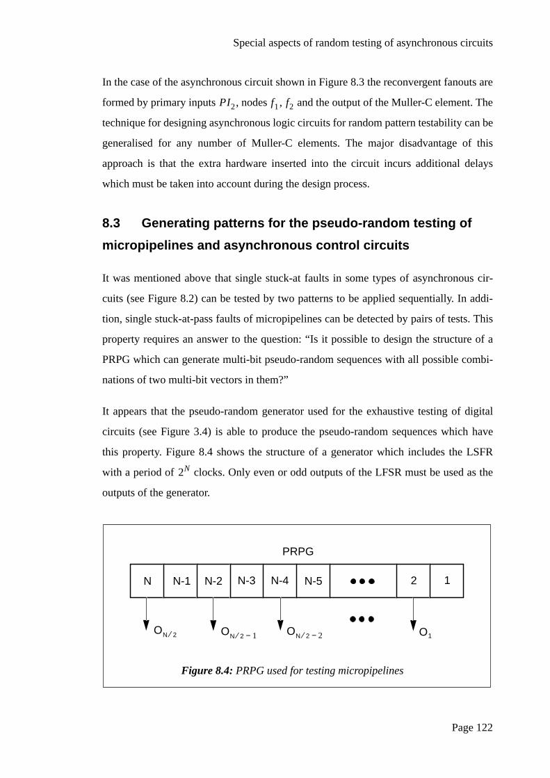
Special aspects of random testing of asynchronous circuits
Page 122
In the case of the asynchronous circuit shown in Figure 8.3 the reconvergent fanouts are
formed by primary inputs , nodes , and the output of the Muller-C element. The
technique for designing asynchronous logic circuits for random pattern testability can be
generalised for any number of Muller-C elements. The major disadvantage of this
approach is that the extra hardware inserted into the circuit incurs additional delays
which must be taken into account during the design process.
8.3 Generating patterns for the pseudo-random testing of
micropipelines and asynchronous control circuits
It was mentioned above that single stuck-at faults in some types of asynchronous cir-
cuits (see Figure 8.2) can be tested by two patterns to be applied sequentially. In addi-
tion, single stuck-at-pass faults of micropipelines can be detected by pairs of tests. This
property requires an answer to the question: “Is it possible to design the structure of a
PRPG which can generate multi-bit pseudo-random sequences with all possible combi-
nations of two multi-bit vectors in them?”
It appears that the pseudo-random generator used for the exhaustive testing of digital
circuits (see Figure 3.4) is able to produce the pseudo-random sequences which have
this property. Figure 8.4 shows the structure of a generator which includes the LSFR
with a period of clocks. Only even or odd outputs of the LFSR must be used as the
outputs of the generator.
PI2 f1 f2
12N N-1 N-2 N-3 N-5N-4
O1ON 2⁄ ON 2 1−⁄ ON 2 2−⁄
PRPG
Figure 8.4: PRPG used for testing micropipelines
2N

Special aspects of random testing of asynchronous circuits
Page 123
The multi-bit pseudo-random sequence generated on the outputs of this PRPG has the
property that during the period of the LFSR it is possible to find all combinations of
two (N/2)-bit vectors inside the sequence.
Table 8.2 contains the states of the 4-bit LFSR and the outputs of the PRPG shown in
Figure 8.4 for 18 clocks. The PRPG uses the fourth and the second outputs of the LFSR
for generating a two-bit pseudo-random sequence (columns headed as and ). The
4-bit LFSR starts to generate pseudo-random patterns from zero state. During the period
of the 4-bit LFSR (16 clocks) all the combinations of 2-bit vectors are generated inside
this sequence. For instance, the combinations: 00 00, 00 01, 00 10 and 00 11 can be
found easily in the output sequence. This is true for any other combinations of two 2-bit
vectors in which 01, 10 or 11 takes first place.
Thus, pseudo-random patterns generated by the proposed PRPG can be used effectively
for detecting all kinds of single stuck-at faults in micropipelines and asynchronous con-
trol circuits without feedback. It should be noted that the micropipeline is tested exhaus-
tively since besides the generation of all possible binary vectors for the exhaustive
testing of the logic blocks of the micropipeline all the combinations of two (N/2)-bit
Table 8.2: State sequence for the two-bit PRPG
State State
0 0 0 0 0 0 0 9 1 1 0 1 1 0
1 1 0 0 0 1 0 10 0 1 1 0 0 1
2 1 1 0 0 1 0 11 0 0 1 1 0 1
3 1 1 1 0 1 1 12 1 0 0 1 1 0
4 1 1 1 1 1 1 13 0 1 0 0 0 0
5 0 1 1 1 0 1 14 0 0 1 0 0 1
6 1 0 1 1 1 1 15 0 0 0 1 0 0
7 0 1 0 1 0 0 16 0 0 0 0 0 0
8 1 0 1 0 1 1 17 1 0 0 0 1 0
Q4 Q3 Q2 Q1 O2 O1 Q4 Q3 Q2 Q1 O2 O1
2N
O1 O2

Special aspects of random testing of asynchronous circuits
Page 124
vectors are produced by the generator for the detection of all single stuck-at-pass faults
in the latches.

Page 125
Chapter 9 : Conclusions and
further work
9.1 Conclusions
Asynchronous VLSI design is becoming a subject of intensive research because of the
possibility of achieving higher performance and lower power consumption on the asyn-
chronous chip in comparison with its synchronous equivalent. More accurately, syn-
chronous design is a special case representing a single point in a multi-dimensional
asynchronous world. There are several approaches to the design of asynchronous digital
circuits. The bounded-delay model is the most attractive approach since it allows for the
design of complex asynchronous networks by using fundamental principles for design-
ing digital circuits and a pipelined approach.
The micropipelined approach used by the AMULET group in the design of an asynchro-
nous version of ARM6 is based on a convention where the data is encoded normally but
is bundled together with control signals called “request” and “acknowledge”. Once
designed it is necessary to ensure that a physical implementation of such a microproces-
sor will work correctly. This can be achieved by applying a set of test patterns to its
inputs and observing the responses on the outputs. The asynchronous implementation of
ARM6 is more complicated than the synchronous one which aggravates the test prob-
lems significantly.
As was shown, the major difficulties in testing both synchronous and asynchronous
VLSI circuits are similar. The general fault models which can be used for representing
fault effects in asynchronous VLSI designs are stuck-at faults, bridging faults, stuck-
open faults and delay faults. Each kind of fault manifests itself differently in asynchro-
nous networks than in synchronous circuits and this requires a more detailed analysis to

Conclusions and further work
Page 126
be done in order to derive effective test vectors. In bounded-delay asynchronous
designs, delay faults are the source of the most difficult test problems to be solved.
Random (pseudo-random) testing is becoming a viable alternative to deterministic test
generation methods for the following reasons:
• the test sequence applied to the inputs of the VLSI circuit does not depend on its
specification and can be used for all the circuits to be tested;
• pseudo-random pattern generators are simple and can be used successfully in asyn-
chronous built-in self-test structures.
The majority of DFT methods have been developed to ease the generation and applica-
tion of test vectors to synchronous circuits. Three groups of DFT techniques can be dis-
tinguished: ad hoc strategies, structured approaches and built-in self-test techniques.
The most popular DFT methods allow for the separation of the combinational part of the
circuit from the memory elements during the test. A particular DFT method can solve a
subset of the test problems concerned with the circuit to be tested. The advantages of
DFT methods for VLSI circuits cannot be achieved without a cost measured usually in
terms of silicon overhead, performance degradation and reduction in reliability.
Testing asynchronous VLSI circuits is a difficult problem mainly because of the differ-
ent approaches to designing these kinds of networks whereas the majority of test gener-
ation methods have been devised for testing synchronous circuits. Analysis of work in
the field of testing asynchronous VLSI circuits shows that there are two main directions
to solve this problem:
• adapting existing test generation techniques for testing synchronous VLSI circuits to
test asynchronous ones;
• deriving new test generation approaches to testing asynchronous VLSI circuits.
Recent results in the testing of micropipelines show that the test procedure of such asyn-
chronous designs must include the testing of both the control part and the data paths of

Conclusions and further work
Page 127
the micropipeline under test. It was proved that single stuck-at faults in the control cir-
cuits of the micropipeline are tested during the normal operation mode whereas two test
patterns are required to detect those faults in the data paths of the micropipeline.
An asynchronous random testing interface has been described in this thesis. It includes
an asynchronous pseudo-random pattern generator and an asynchronous parallel signa-
ture analyser. The correctness of the structures proposed has been checked using stand-
ard CAD tools for simulating hardware designs. A program model of the universal
pseudo-random pattern generator has been developed. This generator can produce multi-
bit pseudo-random sequences without the obvious shift operation, and can also produce
weighted pseudo-random test patterns.
In this thesis, mathematical expressions have been derived for predicting test lengths for
the random pattern testing of micropipelines by using equiprobable and weighted test
patterns. It was shown that to estimate the lower bound for the test length using
equiprobable random test patterns it is possible: 1) to use the assumption that appear-
ances of all test patterns are mutually exclusive events and 2) to exploit the Poisson
approximation for calculating the probabilities of these events. It was proved that to
evaluate more exactly the lower bound for the test length for random testing a combina-
tional network by means of weighted test patterns it is sufficient to take into account the
probability of the rarest test pattern, , and the number of test patterns whose appear-
ance probabilities belong to the range [ ; ]. The theoretical results have been
confirmed by simulation.
The probabilistic properties of then-input Muller-C element have been investigated. It
was proved that from the probabilistic point of view:
• stuck-at-1 (stuck-at-0) faults onk inputs of then-input Muller-C element ( )
are equivalent to a stuck-at-1 (stuck-at-0) fault on its output;
• if (n-1) input signals of then-input Muller-C element are equiprobable and independ-
ent then the Muller-C element can be considered as a line which connects its other
input and the output.
pmin
pmin 2pmin
1 k n≤ ≤
Conclusions and further work
Page 128
It was shown that the optimal random test procedure for the testing of then-input
Muller-C element is random testing by using equiprobable input signals. Using the prob-
abilistic properties of the Muller-C element and multiplexers incorporated into the cir-
cuit a certain class of asynchronous networks can be designed for random pattern
testability.
It was shown how it is possible to produce pseudo-random patterns to test micropipe-
lines exhaustively. The LFSR generating all possible binary vectors is used as a source
of test patterns. To provide the pseudo-exhaustive testing of the micropipeline it is nec-
essary to use only even (odd) outputs of such an LFSR.
9.2 Future work
The work presented in this thesis will provide a basis for my future research. I intend to
continue my work in the field of the random testing of bounded-delay asynchronous cir-
cuits. The main directions of my future research are the following:
• investigating fault effects and elaborating more accurate fault models which may be
different from the classical fault models but must reflect the appropriate technologi-
cal properties of asynchronous VLSI circuits;
• investigating the behaviour of real asynchronous VLSI circuits (the circuits designed
by the AMULET research group) to be tested by equiprobable and weighted random
(pseudo-random) patterns;
• working out techniques for the effective testing of delay faults in the data paths and
control circuits of micropipelines;
• developing techniques for estimating the degree of random pattern testability of asyn-
chronous VLSI circuits;
• research on asynchronous VLSI designs for random pattern testability in a scan envi-
ronment;

Conclusions and further work
Page 129
• developing asynchronous built-in self-test VLSI structures;
• designing a real chip for random pattern testability and estimating its characteristics
in terms of hardware redundancy, performance and reliability.

Page 130
Appendix A : Asynchronous 4-bit
PRPG
A.1 Schematic of the generator
Figure A.1: An asynchronous implementation of the 4-bit PRPG
Asynchronous Parallel Signature Analyser
AOUT
Q4
Q3
Q2Q1
ROUT
SET
TPLH
TPHL
IN
OUT
DELAY
XOR2
C
R
Q
B
A
toggleC
Q1
Q2
R
XOR2INV
REG4
S
Q4
Q3
Q2
Q1
I4
I3
I2
I1
C

Appendix A : Asynchronous 4-bit PRPG
Page 131
A.2 The register of the generator
Figure A.2: An implementation of the 4-bit register of the generator
Q1
Q2
Q3
S
C
CCE
DQ
RD
DFF
CCE
DQ
RD
DFF
CCE
DQ
RD
DFF
CCE
DQ
RD
DFF
I3
I2
Q4
I4
NOR3
XOR2
I1

Appendix A : Asynchronous 4-bit PRPG
Page 132
A.3 Simulation results
Figure A.3: The results of the behavioural simulation of the generator
SET
ROUT
Q1
Q2
Q3
Q4
AOUT
0500n
1u
Time (Seconds)
D i g i t a l
/tmp_mnt/import/r83/users/oleg/powerview/designs/a_prpg4.wfm
Set
Rou
t
Q1
Q2
Q3
Q4
Aou
t
Tim
e

Page 133
Appendix B : Asynchronous 4-bit
parallel signature
analyser
B.1 Schematic of the signature analyser
Figure B.1: An asynchronous implementation of the 4-bit parallel signature analyser
fdr
REG4
R
Q4Q3Q2Q1
I4I3I2I1
C
CR
QB
A
XOR2
XOR2
XOR2
TPLH TPHL
IN OUTDELAY
INV
toggleC
Q1
Q2
RXOR2
I2
I3
I4
I1
RIN
Q1
Q2
Q3
XOR3Q4
SET
AOUT
ROUT/AIN
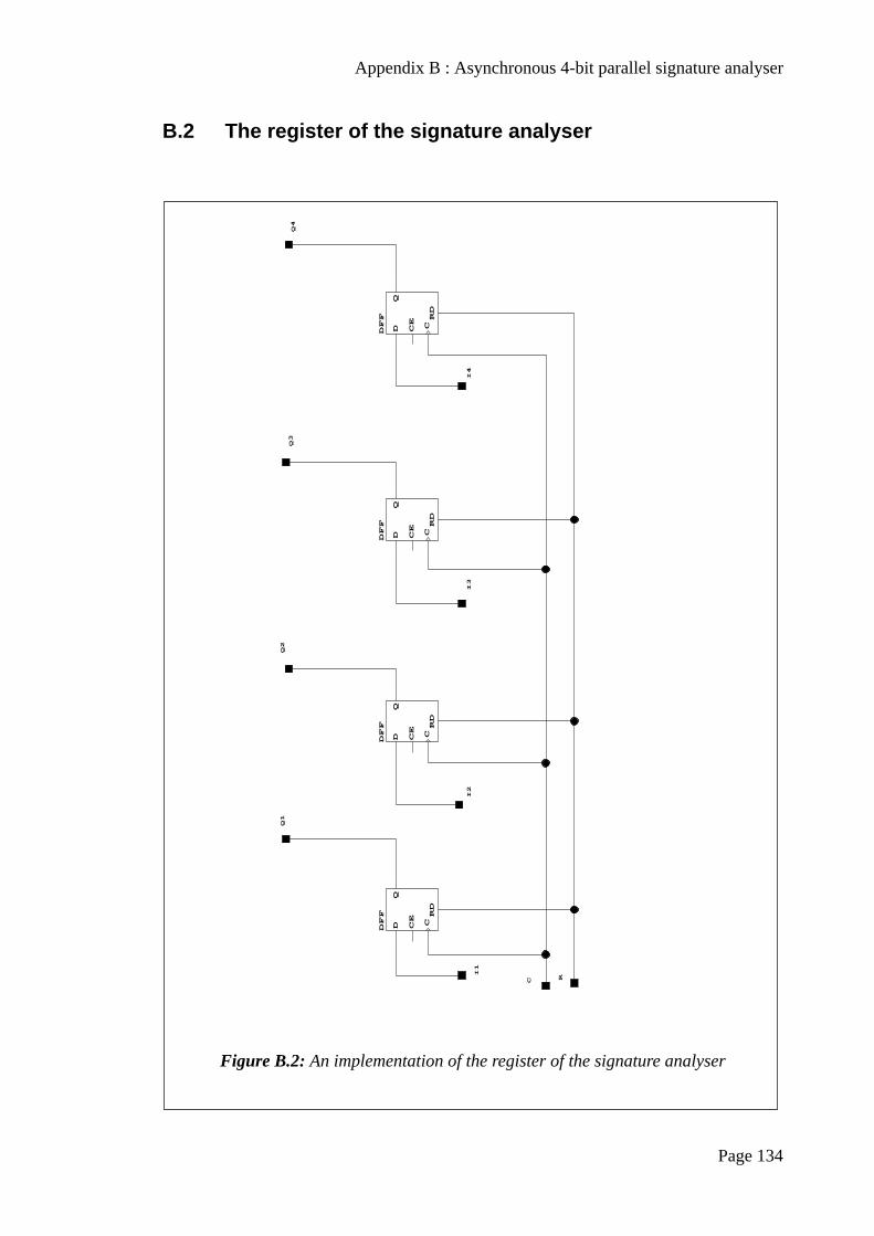
Appendix B : Asynchronous 4-bit parallel signature analyser
Page 134
B.2 The register of the signature analyser
Figure B.2: An implementation of the register of the signature analyser
I4
Q4
Q1
Q3
I2
I3
Q2
I1
CCE
DQ
RD
DFF
CCE
DQ
RD
DFF
CCE
DQ
RD
DFF
CCE
DQ
RD
DFF
C R
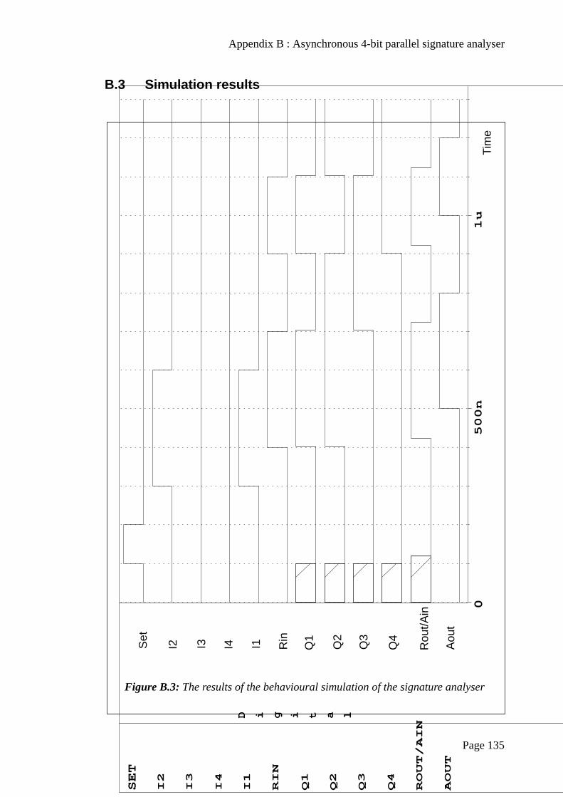
Appendix B : Asynchronous 4-bit parallel signature analyser
Page 135
B.3 Simulation results
Figure B.3: The results of the behavioural simulation of the signature analyser
SET
I2
I3
I4
I1
RIN
Q1
Q2
Q3
Q4
ROUT/AIN
AOUT
0500n
1u
Time (Seconds)
D i g i t a l
/tmp_mnt/import/r83/users/oleg/powerview/designs/a_sign4.wfm
Set
I2 I3 I4 I1 Rin
Q1
Q2
Q3
Q4
Rou
t/Ain
Aou
t
Tim
e

Page 136
References
[1] Russell G. Computer aided tools for VLSI system design. Peter Peregrinus Ltd.,1987.
[2] Mead C., Conway L. Introduction to VLSI systems. Addison-Wesley PublishingCompany, 1980.
[3] Sutherland I.E. Micropipelines. Communications of the ACM, Vol.32, no.6,June, 1989, 720-738.
[4] Gopalakrishnan G., Jain P. Some recent asynchronous system design methodolo-gies. Technical Report UU-CS-TR-90-016, University of Utah, October, 1990.
[5] Furber S. B., Day P., Garside J. D., Paver N. C., Woods J.V. A micropipelinedARM. Proceedings of of the IFIP TCWG 5th International Conference on VLSI,Grenoble, France, 6-10 September 1993, pp. 5.4.1-5.4.10.
[6] Martin A. J., Burns S. M., Lee T. K., Borkovic D., Hazewindus P. J. Design of anasynchronous microprocessor. Advanced Research in VLSI 1989: Proceedingsof the Decennial Caltech Conference on VLSI, ed. C. L. Seitz, MIT Press, 1989,pp. 351-373.
[7] Garside J. D. A CMOS implementation of an asynchronous ALU. Proceedingsof IFIP Working Conference on Asynchronous Design Methodologies / Editedby S. Furber and M. Edwards, Manchester, UK, 31 March - 2 April 1993, 1993,pp. 37-43.
[8] Rice R. Tutorial: VLSI Support Technologies-Computer-Aided Design, Testingand Packaging. IEEE Computer Society, Los Alamitos, Calif., 1982, pp. 228-308.
[9] Russell G., Sayers I. L. Advanced simulation and test methodologies for VLSIdesign. Van Nostrand Reinhold (International), 1989.
[10] Roth J. P. Computer Logic, Testing and Verification. Pitman: Digital SystemDesign Series, London, 1980.
[11] Abramovici M., Breuer M., Fiedman A. D. Digital Systems Testing and TestableDesign. Computer Science Press / Freeman, New York, 1990.
References
Page 137
[12] Cheng Kwang-Ting, Agrawal V. D. Unified Methods for VLSI Simulation andTest Generation. Kluwer Academic, Boston, 1989.
[13] Wilkins B. R. Testing digital circuits : an introduction. Van Nostrand Reinhold(UK), 1986.
[14] Lala P. K. Fault tolerant and fault testable hardware design. Prentice Hall (Inter-national), 1985.
[15] Abraham J. A., Fuchs W. K. Fault and error models for VLSI. Proceedings of theIEEE, Vol.74, no.5, May, 1986, pp. 639-654.
[16] Chen H. H., Mathews R. G., Newkirk J. A. Test generation for MOS circuits.1984 International Test Conference, October, 1984, pp. 70-79.
[17] Agrawal P., Agrawal V. D., Seth S. C. A new method for generating tests fordelay faults in non-scan circuits. Proceedings of the Fifth International Confer-ence on VLSI Design, Bangalore, India, January 1992, pp. 4-11.
[18] Park E. S., Mercer M. R., Williams T. W. A statistical model for delay-fault test-ing. IEEE Design and Test of Computers, February, 1989, pp. 45-55.
[19] Abadir M. S., Reghbati H.K. LSI testing techniques. IEEE Micro, February,1983, pp. 34-51.
[20] Muehldorf E. I., Savkar A. D. LSI logic testing - an overview. IEEE Transactionson Computers, C-30(1), 1981, pp. 1-17.
[21] McCluskey E. J. Built-in self test structures. IEEE Design and Test of Comput-ers, 2(2), 1985, pp. 29-36.
[22] Ibarra O. H., Sahni S. K. Polynomially complete fault detection problems. IEEETransactions on Computers, C-24(3), 1975, pp. 242-249.
[23] McCluskey E. J., Bozorgui-Nesbat S. Design for autonomous test. IEEE Trans-actions on Computers, C-32(2), 1981, pp. 866-875.
[24] Wagner K.D., Chin C.K., McCluskey C.J. Pseudorandom testing. IEEE Transac-tions on Computers, C-36(3), 1987, pp. 332-343.
[25] David R., Thevenod-Fosse P. Random testing of integrated circuits. IEEE Trans-actions on Instrumentation and Measurement, Vol.IM-30(1), March, 1981, pp.20-25.
[26] Hewlett-Packard Ltd. A designer’s guide to signature analysis. Application Note222, 1977.

References
Page 138
[27] Knuth D. E. The art of computer programming. Vol. 2: Seminumerical Algo-rithms, Addison-Wesley Publishing Company, Inc., Reading, Mass., 1969.
[28] McCluskey E. J. Logic design principles: with emphasis on testable semicustomcircuits. Prentice-Hall International Editions, 1986.
[29] Trivedi K.S. Probability and statistics with reliability, queuing and computer sci-ence applications. Englewood Cliffs, NJ: Prentice-Hall, 1982.
[30] Golomb S. W. Shift register sequences. Aegean Park Press, Laguna Hills, Calif.,1982.
[31] McCluskey E. J. Verification testing - a pseudoexhaustive test technique. IEEETransactions on Computers, C-33(6), 1984, pp. 541-546.
[32] Bennetts R. G. Design of testable logic circuits. Addison-Wesley PublishingCompany, 1984.
[33] Williams T.W., Parker K. P. Design for testability - a survey. Proc. IEEE, Vol.71,1983, pp. 95-122.
[34] McCluskey E. J. A survey of design for testability scan techniques. VLSIDesign, 5(12), 1984, pp. 38-61.
[35] Savir J., Ditlow G., Bardell P.H. Random pattern testability. Digest of Papers,13th International Symposium on Fault Tolerant Computing, June, 1983, pp. 80-89.
[36] Le Blanc J. J. LOCST: A built-in self-test technique. IEEE Design and Test, Nov.1984, pp. 45-52.
[37] Bardell P. H., McAnney W. H. Self-testing in a multi-chip logic module. Interna-tional Test Conference, Oct. 1982, IEEE Pub. 82CH1808-5, 1982, pp. 200-204.
[38] Putzolu G. R., Roth J. P. A heuristic algorithm for the testing of asynchronouscircuits. IEEE Transactions on Computers, C-20(6), June 1971, pp. 639-647.
[39] Chappell S. G. Automatic test generation for asynchronous digital circuits. TheBell System Technical Journal, Vol.53, No.8, October 1974, pp. 1477-1503.
[40] Heard B. J., Sheshadri R. N., David R. B., Sammuli A. G. Automatic test patterngeneration for asynchronous networks. 1984 International Test Conference,October 1984, pp. 63-69.
[41] Fujieda T., Zenke N. Testing asynchronous devices. 1987 International Test Con-ference, 1987, pp. 871-875.
References
Page 139
[42] Thorel P., Rainard J. L., Botta A., Chemarin A., Majos J. Implementing bound-ary-scan and pseudo-random BIST in an asynchronous transfer mode switch.1991 International Test Conference, 1991, pp. 131-139.
[43] Bellon C., Velazco R. Taking into account asynchronous signals in functionaltest of complex circuits. Proceedings of the 21st Design Automation Conference,1984, pp. 490-496.
[44] Susskind A. K. A technique for making asynchronous sequential circuits readilytestable. 1984 International Test Conference, 1984, pp. 842-846.
[45] Li T. Design for VLSI asynchronous circuits for testability. Int. J. Electronics,Vol. 64, No. 6, 1988, pp. 859-868.
[46] Keutzer K., Lavagno L., Sangiovanni-Vincentelli A. Synthesis for testabilitytechniques for asynchronous circuits. International Conference on Computer-Aided Designs, 1991, pp. 326-329.
[47] Hazewindus P. Testing Delay-Insensitive Circuits. PhD thesis, Caltech-CS-TR-92-14, California Institute of Technology, 1992.
[48] Roncken M., Saeijs R. Linear test times for delay-insensitive circuits: a compila-tion strategy. Proceedings of IFIP Working Conference on Asynchronous DesignMethodologies / Edited by S. Furber S. and M. Edwards, Manchester, UK, 31March - 2 April 1993, 1993, pp. 13-27.
[49] Beerel P.A., Meng T. H.-Y. Semi-modularity and self-diagnostic asynchronouscontrol circuits. Proceedings of the Conference on Advanced Research in VLSI /editor Carlo H. Sequin, MIT Press, Santa Cruz, March 1991, pp. 103-117.
[50] David I., Ginosar R., Yoeli M. Self-timed is self-diagnostic. Technical Report EEPub No.758, Department of Electrical Engineeing, Technion, November 1990.
[51] Pagey S., Sherlekar S., Venkatesh G. Issues in fault modelling and testing ofmicropipelines, 1994, to appear.
[52] Benowitz N., Calhoun D. F., Alderson G. E., Bauer J. E., Joeckel C. T. Anadvanced fault isolation system for digital logic. IEEE Transactions on Comput-ers, C-21(9), 1972, pp. 1015-1017.
[53] Agrawal P., Agrawal V. D. On Monte Carlo testing of logic tree networks. IEEETransactions on Computers, C-25(6), 1976, pp. 664-667.
[54] Waicukauski J. A., Lindbloom E., Eichelberger F. B. A method for generatingweighted random test patterns. IBM J. Res. and Dev., 1989, no. 2, pp. 149-161.
References
Page 140
[55] Virupakshia A. R., Reddy V. C. A simple random test procedure for detection ofsingle intermittent fault in combinational circuits. IEEE Trans. on Computers,1983, no. 6, pp. 594-597.
[56] J. J. Shedletsky, Random Testing: Practicality vs. Verified Effectiveness, Proc.Seventh Int. Conf. on Fault-Tolerant Comp., June 1977, pp. 175-179
[57] Savir J., Bardell P.H. On random pattern test length. Digest of Papers, 1983International Test Conference, October, 1983, pp. 95-106.
[58] Chin C.K., McCluskey E. J. Test length for pseudorandom testing. IEEE Trans-actions on Computers, C-36(2), 1987, pp. 252-256.
[59] Bostock L. , Chandler S. Pure Mathematics. Stanley Thornes (Publishers) Ltd.,1984.
[60] Spiegel M. R. Mathematical Handbook of Formulas and Tables. McGraw-HillBook Company, 1968.
[61] Parker K.P., McCluskey E. J. Analysis of logic circuits with faults using inputsignal probabilities. IEEE Transactions on Computers, C-24(5), 1975, pp. 573-578.
[62] Parker K.P., McCluskey E. J. Probabilistic treatment of general combinationalnetworks. IEEE Transactions on Computers, C-24(6), 1975, pp. 668-670.
[63] Seth S. C., Agrawal V. D. A new model for computation of probabilistic testabil-ity in combinational circuits. Intergation, The VLSI Journal, No.7, 1989, pp. 49-75.