Radeon R5xx Acceleration
262
Revision 1.1 February 22, 2008 © 2008 Advanced Micro Devices, Inc. Proprietary 1 Radeon R5xx Acceleration
Transcript of Radeon R5xx Acceleration

Revision 1.1 February 22, 2008
© 2008 Advanced Micro Devices, Inc. Proprietary 1
Radeon R5xx Acceleration
Revision 1.1 February 22, 2008
© 2008 Advanced Micro Devices, Inc. Proprietary 2
Trademarks AMD, the AMD Arrow logo, Athlon, and combinations thereof, ATI, ATI logo, Radeon, and Crossfire are trademarks of Advanced Micro Devices, Inc. Microsoft and Windows are registered trademarks of Microsoft Corporation. Other product names used in this publication are for identification purposes only and may be trademarks of their respective companies. Disclaimer The contents of this document are provided in connection with Advanced Micro Devices, Inc. ("AMD") products. AMD makes no representations or warranties with respect to the accuracy or completeness of the contents of this publication and reserves the right to make changes to specifications and product descriptions at any time without notice. No license, whether express, implied, arising by estoppel, or otherwise, to any intellectual property rights are granted by this publication. Except as set forth in AMD's Standard Terms and Conditions of Sale, AMD assumes no liability whatsoever, and disclaims any express or implied warranty, relating to its products including, but not limited to, the implied warranty of merchantability, fitness for a particular purpose, or infringement of any intellectual property right. AMD's products are not designed, intended, authorized or warranted for use as components in systems intended for surgical implant into the body, or in other applications intended to support or sustain life, or in any other application in which the failure of AMD's product could create a situation where personal injury, death, or severe property or environmental damage may occur. AMD reserves the right to discontinue or make changes to its products at any time without notice. © 2008 Advanced Micro Devices, Inc. All rights reserved.
Revision 1.1 February 22, 2008
© 2008 Advanced Micro Devices, Inc. Proprietary 3
1. INTRODUCTION ............................................................................................................................................. 6
1.1 INTRODUCING THE R5XX FAMILY .......................................................................................................................... 6
1.2 FEATURE HIGHLIGHTS ........................................................................................................................................ 6
1.3 FEATURES IN DETAIL .......................................................................................................................................... 6
1.4 CHANGES FROM R3XX/4XX ................................................................................................................................. 7
2. TILING............................................................................................................................................................ 9
2.1 OVERVIEW ....................................................................................................................................................... 9
2.2 MICRO BLOCKS ................................................................................................................................................. 9
2.3 MACRO BLOCKS ................................................................................................................................................ 9
3. SURFACE FORMATS ..................................................................................................................................... 11
4. COMMAND PROCESSOR .............................................................................................................................. 13
4.1 OVERVIEW ..................................................................................................................................................... 13
4.2 HOST PROGRAMMING MODEL DESCRIPTION ........................................................................................................ 13
4.3 PUSH VS PULL MODEL ..................................................................................................................................... 13
4.4 RING BUFFER MANAGEMENT ............................................................................................................................ 14
4.5 CHIPSET COHERENCY ISSUES .............................................................................................................................. 16
4.6 INDIRECT BUFFER MANAGEMENT ....................................................................................................................... 16
4.7 OVERVIEW OF DMA OPERATION ....................................................................................................................... 17
4.8 RESETTING THE COMMAND PROCESSOR .............................................................................................................. 19
4.9 COMMAND STREAM SYNCHRONIZATION .............................................................................................................. 19
4.10 STARTING THE INDIRECT STREAMS ...................................................................................................................... 20
4.11 WRITING HOST DATA TO THE COMMAND STREAM QUEUE ..................................................................................... 21
4.12 WRITING TO THE MICROENGINE RAM ............................................................................................................... 22
4.13 READING FROM THE MICROENGINE RAM ........................................................................................................... 22
4.14 STARTING A DMA OPERATION .......................................................................................................................... 23
5. PM4 ............................................................................................................................................................. 24
5.1 PACKET TYPES ................................................................................................................................................ 24
5.2 DEFINITION OF TYPE-3 PACKETS ......................................................................................................................... 28
6. VERTEX SHADERS ........................................................................................................................................ 54
6.1 INTRODUCTION ............................................................................................................................................... 54
6.2 INPUT ........................................................................................................................................................... 54
6.3 VECTOR ORDER AND VECTOR ID’S ...................................................................................................................... 59
6.4 VAP REGISTERS .............................................................................................................................................. 60
6.5 R3XX-R5XX PROGRAMMABLE VERTEX SHADER DESCRIPTION .................................................................................. 66
7. FRAGMENT SHADERS .................................................................................................................................. 94
7.1 INTRODUCTION ............................................................................................................................................... 94
7.2 INSTRUCTIONS ................................................................................................................................................ 94

Revision 1.1 February 22, 2008
© 2008 Advanced Micro Devices, Inc. Proprietary 4
7.3 INSTRUCTION WORDS ...................................................................................................................................... 95
7.4 ALU INSTRUCTIONS ......................................................................................................................................... 96
7.5 TEXTURE INSTRUCTIONS ................................................................................................................................. 104
7.6 FLOW CONTROL ............................................................................................................................................ 106
7.7 FLOATING POINT ISSUES ................................................................................................................................. 112
7.8 WRITING TO US REGISTERS ............................................................................................................................. 115
8. HIZ ............................................................................................................................................................. 117
8.1 INTRODUCTION ............................................................................................................................................. 117
8.2 ENABLING HIZ .............................................................................................................................................. 117
8.3 CONFIGURING HIZ ........................................................................................................................................ 117
8.4 HIZ CLEAR WITH PM4 PACKET ........................................................................................................................ 119
8.5 EXAMPLE: PUTTING IT ALL TOGETHER ............................................................................................................... 119
8.6 STATE CHANGES THAT INVALIDATE HIZ ............................................................................................................. 120
9. DRIVER NOTES ........................................................................................................................................... 121
9.1 R5XX CHANGES ............................................................................................................................................ 121
9.2 INTERFACE NOTES ......................................................................................................................................... 123
9.3 REGISTER NOTES ........................................................................................................................................... 124
9.4 FEATURE NOTES ........................................................................................................................................... 129
9.5 BLEND OPTIMIZATION NOTES ........................................................................................................................... 132
9.6 TEXTURE NOTES ............................................................................................................................................ 132
9.7 ERRATA ....................................................................................................................................................... 133
10. REGISTERS ............................................................................................................................................. 134
10.1 COLOR BUFFER REGISTERS .............................................................................................................................. 134
10.2 FOG REGISTERS ............................................................................................................................................. 150
10.3 GEOMETRY ASSEMBLY REGISTERS .................................................................................................................... 153
10.4 GRAPHICS BACKEND REGISTERS ....................................................................................................................... 164
10.5 RASTERIZER REGISTERS ................................................................................................................................... 173
10.6 CLIPPING REGISTERS ...................................................................................................................................... 176
10.7 SETUP UNIT REGISTERS .................................................................................................................................. 184
10.8 TEXTURE REGISTERS....................................................................................................................................... 192
10.9 FRAGMENT SHADER REGISTERS ........................................................................................................................ 203
10.10 VERTEX REGISTERS .................................................................................................................................... 228
10.11 Z BUFFER REGISTERS ................................................................................................................................. 253

Revision 1.1 February 22, 2008
© 2008 Advanced Micro Devices, Inc. Proprietary 5
Revision 1.1 February 22, 2008
© 2008 Advanced Micro Devices, Inc. Proprietary 6
1. Introduction
1.1 Introducing the R5xx Family
The R5xx family provides the fastest and most advanced 2D, 3D, and multimedia graphics performance for desktop
PCs in the performance mainstream markets. The R5xx family supports Shader Model 3.0, advanced memory
interface technology, a brand new display controller and a consumer electronics (CE) quality TV (NTSC/PAL)
encoder. The R5xx family represents AMD‟s 2nd generation PCI Express technology product and leverages a brand
new graphics architecture. The R5xx family builds on the R3xx architecture. As such, much of this guide is
applicable to R3xx and R4xx chips as well with some caveats. Where applicable, generational differences are noted.
1.2 Feature Highlights
1.2.1 Shader Technology
Support for Microsoft® DirectX® 9.0 programmable vertex and pixel shaders in hardware.
Shader Model 3.0 vertex and pixel shader support.
Full speed 32-bit floating point processing.
High dynamic range rendering with floating point blending and anti-aliasing support.
High performance dynamic branching and flow control.
Complete feature set also supported in OpenGL® 2.0.
1.2.2 Anti-Aliasing
2x/4x/6x Anti-Aliasing modes.
Sparse multi-sample algorithm with gamma correction, programmable sample patterns, and centroid
sampling.
New Adaptive Anti-Aliasing mode.
Temporal Anti-Aliasing.
Lossless Color Compression (up to 6:1) at all resolutions, up to and including widescreen HDTV.
1.2.3 New Ring Bus Memory Controller
Programmable arbitration logic maximizes memory efficiency, software upgradeable.
New fully associative texture, color, and Z cache design.
Hierarchical Z-Buffer with Early Z Test.
Lossless Z-Buffer Compression (up to 48:1).
Fast Z-Buffer Clear.
Z Cache optimized for real-time shadow rendering.
Optimized for performance at high display resolutions, up to and including widescreen HDTV.
1.3 Features in Detail
1.3.1 2D Acceleration Features
A highly optimized 128-bit engine, capable of processing multiple pixels/clock.

Revision 1.1 February 22, 2008
© 2008 Advanced Micro Devices, Inc. Proprietary 7
Hardware acceleration provided for BitBLT, line drawing, polygon and rectangle fills, bit masking,
monochrome expansion, panning and scrolling, scissoring, and full ROP support (including ROP3).
Optimized handling of fonts and text using ATI proprietary techniques.
Game acceleration including support for Microsoft's DirectDraw: Double Buffering, Virtual Sprites,
Transparent BLT, and Masked BLT.
Acceleration in 8/15/16/32-bpp modes.
Support for WIN 2000 & WIN XP GDI extensions: Alpha BLT, Transparent BLT, Gradient Fill.
Hardware cursor support up to 64x64x32-bpp, with alpha channel for direct support of WIN 2000 & WIN
XP alpha cursor standard.
1.3.2 3D Acceleration Features
Fully DirectX 9.0 compliant, including full speed 32-bit floating point per component operations.
Shader Model 3.0 support with programmable vertex shaders (full operand and operation support) allowing
up to 1024 instructions and 256 vectors of constant store. This includes vertex shader loops, branches, and
subroutines, which allow support of the following:
o 1024 vertex shader instruction store.
o 261,888 instructions with a single loop.
o 4+ trillion instructions with nested loops.
o Dynamic flow control.
o 8 full vertex processing units.
Advanced pixel shaders with the following features:
o New advanced shader design, with ultra-threading sequencer for high efficiency operations.
o Full Pixel Shader 3.0 support.
o Advanced, high performance branching support.
o 32-bit floating point support for high dynamic range computations.
Full anti-aliasing on render surfaces up to and including 64-bit floating point formats.
Support for 2xAA, 4xAA and 6xAA subsamples, with little performance loss in most cases.
Advanced AA quality algorithms, generating visuals that are superior to other solutions with an equivalent
number of samples.
New adaptive anti-aliasing modes dynamically select between fast multi-sampling and high quality super-
sampling per polygon, delivering the benefits of both techniques.
1.4 Changes from R3xx/4xx
Changes from R3xx to R4xx
Support for 1, 2, 3 and 4 quad pixel pipes
Support for 1 to 6 vertex shader pipes
HDTV resolution support for HiZ
Support of 16x16 and 32x32 pixel tile sizes (32x32 should now be the preferred amount)
Vastly redesigned Memory controller, with new client interfaces
Support for 8b of subpixel precision
Native support of 4Kx4K raster target
PS instruction support now at 512 each for Scalar, Vec3 and Texture (1536 total instructions)
VS native support for Sin/Cos
TX Component swizzling
Enhanced texture performance
MRT and wide pixel performance fixes

Revision 1.1 February 22, 2008
© 2008 Advanced Micro Devices, Inc. Proprietary 8
Fog alpha rounding matches RGB
Line stipple fixes; SU texture stuffing improvements
LOD Clamp/bias re-order
2D support for larger pixels (Pitch at 16b)
4x AA buffer tiling is changed when memory mapping is not used
Changes from R4xx to R5xx
New Memory controller
Support of VS3.0 features, except Vertex fetch
Support of all PS3.0 features, including extended GPRs and Constants, all branching and predication
New FP32 US, including most IEEE NANs, INFs behavior corrected (still TRUNC rounding mode)
Support of new Z range [-2,2], with per pixel clamping in SC
Support of up to 11 texture sets (10 explicit), or 44 iterators
Support of color to texture mappings, and texture to color mappings (for performance improvements)
New IS_IP for better mapping of components from VS to PS
Color now in FP20 mode, instead of S3.12 mode
New HiZ compression mode, allows high precision Z values to be stored
New FP16 render surfaces support, including blending and all backend functions, but not texture filtering
Fully set associative caches for Texture, Color, and Z
New more efficient fifos for all MC clients
New Filter4 mode for Texture unit
New 1b texture mode for texture unit
Revision 1.1 February 22, 2008
© 2008 Advanced Micro Devices, Inc. Proprietary 9
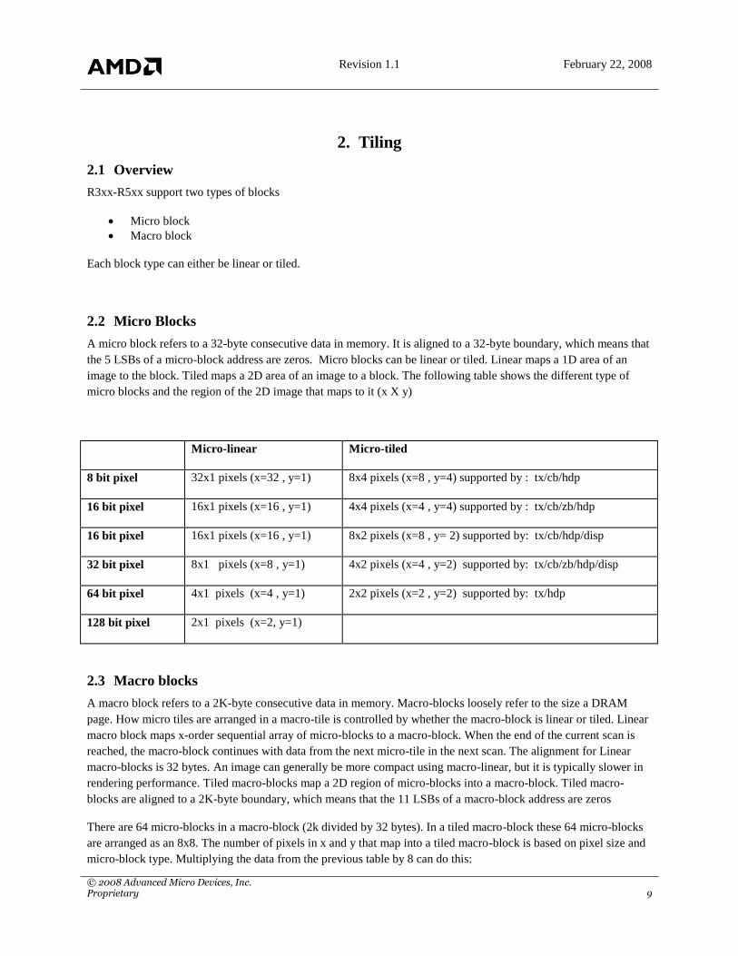
2. Tiling
2.1 Overview
R3xx-R5xx support two types of blocks
Micro block
Macro block
Each block type can either be linear or tiled.
2.2 Micro Blocks
A micro block refers to a 32-byte consecutive data in memory. It is aligned to a 32-byte boundary, which means that
the 5 LSBs of a micro-block address are zeros. Micro blocks can be linear or tiled. Linear maps a 1D area of an
image to the block. Tiled maps a 2D area of an image to a block. The following table shows the different type of
micro blocks and the region of the 2D image that maps to it (x X y)
Micro-linear Micro-tiled
8 bit pixel 32x1 pixels (x=32 , y=1) 8x4 pixels (x=8 , y=4) supported by : tx/cb/hdp
16 bit pixel 16x1 pixels (x=16 , y=1) 4x4 pixels (x=4 , y=4) supported by : tx/cb/zb/hdp
16 bit pixel 16x1 pixels (x=16 , y=1) 8x2 pixels (x=8 , y= 2) supported by: tx/cb/hdp/disp
32 bit pixel 8x1 pixels (x=8 , y=1) 4x2 pixels (x=4 , y=2) supported by: tx/cb/zb/hdp/disp
64 bit pixel 4x1 pixels (x=4 , y=1) 2x2 pixels (x=2 , y=2) supported by: tx/hdp
128 bit pixel 2x1 pixels (x=2, y=1)
2.3 Macro blocks
A macro block refers to a 2K-byte consecutive data in memory. Macro-blocks loosely refer to the size a DRAM
page. How micro tiles are arranged in a macro-tile is controlled by whether the macro-block is linear or tiled. Linear
macro block maps x-order sequential array of micro-blocks to a macro-block. When the end of the current scan is
reached, the macro-block continues with data from the next micro-tile in the next scan. The alignment for Linear
macro-blocks is 32 bytes. An image can generally be more compact using macro-linear, but it is typically slower in
rendering performance. Tiled macro-blocks map a 2D region of micro-blocks into a macro-block. Tiled macro-
blocks are aligned to a 2K-byte boundary, which means that the 11 LSBs of a macro-block address are zeros
There are 64 micro-blocks in a macro-block (2k divided by 32 bytes). In a tiled macro-block these 64 micro-blocks
are arranged as an 8x8. The number of pixels in x and y that map into a tiled macro-block is based on pixel size and
micro-block type. Multiplying the data from the previous table by 8 can do this:

Revision 1.1 February 22, 2008
© 2008 Advanced Micro Devices, Inc. Proprietary 10
Macro-tiled
Micro-linear
Macro-tiled
Micro-tiled
8 bit pixel 256x8 64x32
16 bit pixel (8x2) 128x8 64x16
16 bit pixel (4x4) 128x8 32x32
32 bit pixel 64x8 32x16
64 bit pixel 32x8 16x16
Revision 1.1 February 22, 2008
© 2008 Advanced Micro Devices, Inc. Proprietary 11
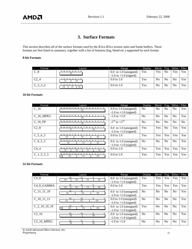
3. Surface Formats
This section describes all of the surface formats used by the R3xx-R5xx texture units and frame buffers. These
formats are first listed in summary, together with a list of features (fog, blend etc.) supported by each format.
8-bit Formats
Format Layout Range Display Blend Fog Dither Filter
C_8 01234567C0
0.0 to 1.0 (unsigned)
-1.0 to +1.0 (signed)
Yes Yes No Yes Yes
C2_4 01234567C0C1
0.0 to 1.0 Yes No No No Yes
C_3_3_2 01234567C0C2 C1
0.0 to 1.0 Yes No No No Yes
16-bit Formats
Format Layout Range Display Blend Fog Dither Filter
C_16 89101112131415 01234567C0
0.0 to 1.0 (unsigned)
-1.0 to +1.0 (signed)
No No No No Yes
C_16_MPEG 89101112131415 01234567C0
-1.0 to +1.0 No No No No Yes
C_16_FP 89101112131415 01234567C0
-2
16 to +2
16 No No No No No
C2_8 C1
89101112131415 01234567C0
0.0 to 1.0 (unsigned)
-1.0 to +1.0 (signed)
Yes Yes No Yes Yes
C_5_6_5 C2
89101112131415 01234567C0C1
0.0 to 1.0 Yes Yes Yes Yes Yes
C_6_5_5 C2
89101112131415 01234567C0C1
0.0 to 1.0 (unsigned)
-1.0 to +1.0 (signed)
No No No No Yes
C4_4 C3
89101112131415 01234567C0C1C2
0.0 to 1.0 Yes Yes Yes Yes Yes
C_1_5_5_5 C1
89101112131415 01234567C0C2C3
0.0 to 1.0 Yes Yes Yes Yes Yes
32-bit Formats
Format Layout Range Display Blend Fog Dither Filter
C4_8 1624 08C0C1C2C3
0.0 to 1.0 (unsigned)
-1.0 to +1.0 (signed)
Yes Yes Yes Yes Yes
C4_8_GAMMA 1624 08C0C1C2C3
0.0 to 1.0 Yes Yes Yes Yes Yes
C_11_11_10 1624 08C0C1C2
0.0 to 1.0 (unsigned)
-1.0 to +1.0 (signed)
No No No No Yes
C_10_11_11 1624 08C0C1C2
0.0 to 1.0 (unsigned)
-1.0 to +1.0 (signed)
No No No No Yes
C_2_10_10_10 1624 08C0C1C2C3
0.0 to 1.0 (unsigned)
-1.0 to +1.0 (signed)
Yes No No No Yes
C2_16 1624 08C1 C0
0.0 to 1.0 (unsigned)
-1.0 to +1.0 (signed)
No No No No Yes
C2_16_MPEG 1624 08C1 C0
-1.0 to +1.0 No No No No Yes

Revision 1.1 February 22, 2008
© 2008 Advanced Micro Devices, Inc. Proprietary 12
C2_16_FP 1624 08C1 C0
-2
16 to +2
16 No No No No No
C_32_FP 1624 08C0
-2
127 to +2
127 No No No No No
C_AVYU 1624 08A UYV
0.0 to 1.0 Yes Yes Yes Yes Yes
C_VYUY 1624 08V Y1 V Y0
0.0 to 1.0 Yes Yes Yes Yes Yes
C_YVYU 1624 08Y1 V Y0 U
0.0 to 1.0 Yes Yes Yes Yes Yes
64-bit Formats
Format Layout Range Display Blend Fog Dither Filter
C4_16 C3
3248 0164056 824C2 C1 C0
0.0 to 1.0 (unsigned)
-1.0 to +1.0 (signed)
No No No No Yes
C4_16_FP C3
3248 0164056 824C2 C1 C0
-2
16 to +2
16 No No No No No
C2_32_FP C1
3248 0164056 824C0
-2
127 to +2
127 No No No No No
128-bit Formats
Format Layout Range Display Blend Fog Dither Filter
C4_32_FP C3
6496 03280112 1648C2 C1 C0
-2
127 to +2
127 No No No No No
Depth Formats
Format Layout Range Write Read
W_24 1624 8DEPTH
0
0 to 2
24-1 Yes No
W_24_FP 1624 8DEPTH
0
-2
63 to +2
63 Yes Yes
Revision 1.1 February 22, 2008
© 2008 Advanced Micro Devices, Inc. Proprietary 13
4. Command Processor
4.1 Overview
The Command Processor is a programmable processor that is meant to provide some on-chip intelligence for a
Graphics Controller device. The CP architecture has been approached as a special-purpose computing engine,
targeted at fetching and interpreting a PROMO4 command stream.
The Command Processor takes on several tasks in a typical Graphics Controller:
Acts as a receiver of command streams from the video and graphics device driver(s) running on the host
CPU. These command streams are either read from system memory using bus-mastering on the PCI or
AGP bus, or directly written to the CP from the host CPU using the PCI or AGP (fast-write) bus. Three
streams are supported – one Ring Buffer and two Indirect Buffers.
Parses and interprets a command stream, and writes the parsed data to internal “Feature” modules of the
Graphics Controller device; for example, a 3D graphics processor, a 2D graphics processor, a Video
Processor, or an MPEG Decoder. The data writes can be 32, 64, 96, or 128 bits per clock. The 64, 96, and
128 bit writes will occur for “Vector Write Mode”. Vector write mode is valid when the stream (PQ, IQ1,
IQ2) is in Pull Mode. Push mode will only write DWORDs (i.e. Lower 32-bits of the 128-bit data bus will
be valid with a DWORD_Enable = “0001”. The 64 and 96-bit writes will only occur while the alignment of
the data is not on a 128-bit boundary.
There are two general-purpose DMA engines inside the CP, one for GUI-related tasks, and one intended for
Video Capture tasks. The DMA engines do byte alignment between the source and destination surfaces.
4.2 Host Programming Model Description
This section describes the manner in which the host CPU communicates with the graphics controller chip.
4.3 Push vs Pull Model
The Push Model is also referred to as Programmed I/O (PIO). In this model the host CPU is writing to the graphics
controller chip across either the PCI or AGP bus. That is, the host is “pushing” command information to the
graphics controller. This information is in one of two forms:
1) A sequence of register writes to setup the state of a processing engine on the graphics controller, and
then starting the engine running. Typically, engines are started as a side-effect of writing to a special
“trigger” or “initiator” register.
2) A sequence of Command Packets, which are a “compressed” way of conveying the command
information to the graphics controller, relying on an intelligent processor in the graphics controller to
convert the command packets into register writes to other processing engines in the graphics controller.
It is expected that option (1) above will only be used for debug purposes.
The Pull Model utilizes bus-mastering on the part of the graphics controller, as it actively goes out and reads from an
area of system memory in which the host CPU has previously placed command information. An important part of
the pull model is how the host and the graphics controller manage access to the shared buffer in system memory.
This is discussed in the following section.
The pull model allows more slip between the CPU and the graphics controller than does the push model, assuming
that the command buffer for the push model is limited to on-chip storage.
The push model may have some advantage when the overall system performance is taken into account as it lightens
the bandwidth demand on system memory as compared to the pull model. The push model may be able to make-up

Revision 1.1 February 22, 2008
© 2008 Advanced Micro Devices, Inc. Proprietary 14
for its limited slip by implementing an on-chip command buffer that “spills-over” into the frame buffer; however,
this of course begins to place a demand on the frame buffer bandwidth to write and read the command buffer.
The Command Processor will support both the push and pull models; however, switching between these two models
must be carefully controlled. It is intended that switching is not done often; most likely the model is chosen at reset
time, and never changed once the system is running. The pull model is the preferred choice for systems that allow
bus-mastering, and whose API allows concurrent processing between the host CPU and the graphics controller,
primarily because of its superior capability for overlapped processing. The push model is available for systems that
are not well-suited to using the pull model.
4.4 Ring Buffer Management
When the Graphics Controller is set to operate in the bus-mastering mode (pull model), the host application, say a
driver, has to allocate a block of system memory as a buffer for the command packets it issues to the Graphics
Controller. The command packets, or simply packets, instruct the Graphics Controller to carry out operations such
as drawing objects on the screen. This memory block is treated as if it is a ring that allows the packets to be placed
into and taken away from the memory in a circular manner, thus the name Ring Buffer.
The Ring Buffer is a shared memory space between two cooperating processors. It is used to implement one-way
communication from the Host processor (the Writer) to the Graphics Controller (the Reader). Each processor must
maintain the state that it believes that the Ring Buffer is in. The state is composed of:
Buffer Base: The address of the beginning of the buffer.
Buffer Size: The size of the buffer.
Write Pointer: The address that the Host is writing to.
Read Pointer: The address that the Graphics Controller is reading from.
In order for the Ring Buffer to work properly, both processors must maintain a consistent view of this state. The
Buffer Base and Buffer Size are generally initialized when the system is first brought-up, and rarely changed after
that point. It is a simple task to initialize both the Reader‟s and the Writer‟s copies of this state. The Read and
Write Pointers, on the other hand, change quite frequently as the Ring Buffer is in operation. In order to achieve
consistency, when the Writer (the host) updates the Write Pointer, he must send that value to the Reader‟s (the
Graphics Controller‟s) copy of the Write Pointer. And similarly, when the Reader updates the Read Pointer, he must
send that value to the Writer‟s copy of the Read Pointer.
Packets are placed into the memory block, or buffer, from the beginning towards the end, i.e., from lower addresses
toward higher addresses. Once the data placement hits the end, it starts from the beginning again. Meanwhile, the
packets are consumed from the head of the queue in a manner similar to how they were placed.
Figure illustrates how the ring buffer operates when combined with the bus-mastering operation.

Revision 1.1 February 22, 2008
© 2008 Advanced Micro Devices, Inc. Proprietary 15
PN
P2
P1
free area
Ring Buffer
Server
Graphics
ControllerHost
Ring Buffer
Buffer Size
Write Pointer
Buffer Base
Read Pointer
Execution
UnitMemoryRegisterLegend:
end of bufferstart of buffer
data flow
Packets Bus
Mastering
Unit
Write Pointer
Buffer Base
Read Pointer
Buffer Size
Read Pointer
Address
Co
mm
an
d P
ack
et
Bu
ffer
Driver(s)
PN-1
Write Pointer Address
Figure: Ring Buffer and its Control Structure
In the figure, packets are placed into the buffer in a counter-clockwise order, forming a packet queue. The first
packet in the queue is denoted by P1 , and the last by Pn . The start of the queue, P1 , is pointed to by the Read
Pointer(s). The memory portion that is not occupied by packets is called the free area, and it is pointed to by the
Write Pointer(s).
Initially, both the read and write pointers may point to the same location of the ring buffer, e.g. the start of the
memory block. The two pointers pointing to the same location of the ring buffer generally implies one of two
situations. One is that the buffer is empty, and the other is that the buffer is full. We want to define this situation as
an empty buffer. To resolve the ambiguity of both pointers being equal, we must prevent the case of a full buffer
from ever happening. It is the Host‟s responsibility to ensure that there is at least one free location in the buffer.
On the host side, the driver places command packets into the free area of the ring buffer, and informs the Graphics
Controller of any changes to the Write Pointer by writing directly to the Write Pointer register inside the Graphics
Controller. The host tracks free-space in the buffer by comparing its Read and Write Pointers, and suspends writing
if the buffer becomes (almost) full.
On the Graphics Controller side, packets are taken away one-by-one from the head of the packet queue, pointed to
by its Read Pointer, through the Host Bus Interface, and placed into the Command Packet Buffer. As the Graphics
Controller updates its copy of the Read Pointer, it uses a bus-mastering write to update the Host‟s copy of the Read
Pointer, residing in a shared memory location. The Graphics Controller has a register that holds the memory address
of where the Host‟s Read Pointer resides, and uses that for the address of the bus-mastering write. The Graphics
Controller tracks free-space in the buffer by comparing its Read and Write Pointers, and suspends reading if the
buffer becomes empty (i.e., Read Pointer == Write Pointer).
To reduce traffic on the system memory bus, the Graphics Controller should not update the Host‟s copy of the Read
Pointer every time it changes on the Graphics Controller side. To facilitate this, we have adopted a concept of a

Revision 1.1 February 22, 2008
© 2008 Advanced Micro Devices, Inc. Proprietary 16
block of dwords in the packet queue. The Graphics Controller will update the host‟s copy of the Read Pointer every
time it has consumed a “block‟s-worth” of data from the ring buffer. The other time when the Graphics Controller
will update the Read Pointer is when it thinks that the packet queue is empty. The size of the block is
programmable, to allow the programmer to trade-off the amount of time the system bus spends doing real data
transfer vs the amount of time it spends on the communication overhead of updating read/write pointers. Larger
block sizes tend to reduce communication overhead, at the “expense” of reducing the number of blocks in the queue,
which reduces the amount of “slip” (or de-coupling) between the Host and the Graphics Controller.
To reduce traffic on the system memory bus, the driver may want to minimize the frequency of accesses to its copies
of the Read and Write Pointers. To minimize reads of the Read Pointer, it can check them once, calculate an amount
of free space, and then decrement a local copy of the amount of free space as it adds packets to the queue. When it
sees that the free-space is small (queue nearly full), it can start this procedure over again. (Its copy of the Read
Pointer may have changed since the last time he read it.) The host also has the option of updating the Graphics
Controller‟s Write Pointer on a less-frequent basis than with every write he does to the packet queue, possibly on a
block-basis similar to the Graphics Controller‟s mechanism. However, if the buffer is running close to empty, any
delay in updating the Graphics Controller‟s Write Pointer may add latency to the Graphics Controller‟s response to
this command packet. Also, the host must be careful to update the Graphics Controller‟s copy of the Write Pointer
if it wants the Graphics Controller to read from the queue until it is empty.
When the queue has become (almost) full, the host will have to poll the Read Pointer until space becomes available.
In certain systems (Pentium II for example), this polling will stay within the processor cache, thus avoiding traffic
on the system bus, and the snoop logic of the host CPU will take care of maintaining consistency between the main
memory and the processor cache when the Graphics Controller performs its bus-mastering write of the Read Pointer.
It is important to note that the Read Pointer must reside in PCI space in order for this snoop technique to work.
AGP writes are not snooped.
4.5 Chipset Coherency Issues
The Rage128 product revealed a weakness in some motherboard chipsets in that there is no mechanism to guarantee
that data written by the CPU to memory is actually in a readable state before the Graphics Controller receives an
update to its copy of the Write Pointer. In an effort to alleviate this problem, we‟ve introduced a mechanism into the
Graphics Controller that will delay the actual write to the Write Pointer for some programmable amount of time, in
order to give the chipset time to flush its internal write buffers to memory.
There are two register fields that control this mechanism: PRE_WRITE_TIMER and PRE_WRITE_LIMIT. There
is also a staging register placed “in front of” the actual Write Pointer register of the CP. All host writes go into the
staging register and are held there until one of two events occurs: the down-counter of PRE_WRITE_TIMER has
expired; or the host has written the staging register PRE_WRITE_LIMIT-times, forcing the contents of the staging
register into the actual Write Pointer register. The down-counter is seeded with PRE_WRITE_TIMER every time
the host writes to the Write Pointer register address, and expires when it reaches zero. This implementation does not
guarantee a certain time-delay between the host write to the Write Pointer, and the Graphics Controller read of the
system memory; because the host could flood the Graphics Controller with multiple writes (more than the
PRE_WRITE_LIMIT) in a short amount of time, thus overriding the time-delay imposed by the
PRE_WRITE_TIMER. However, since the normal operation of this system is to increase the Write Pointer by some
significant amount with each write, it is likely that by the time the PRE_WRITE_LIMIT has been reached, the data
has in fact been “pushed” through the chipset‟s write buffer by subsequent writes to the ring buffer in system
memory.
Note that programming the PRE_WRITE_TIMER and PRE_WRITE_LIMIT to zero allows the chip to behave just
as the Rage128 did.
The above solution is based on a time delay, the assumption being that if the chipset is given enough time, the write
buffer will be flushed to memory, and become available for a coherent read.
4.6 Indirect Buffer Management
The Command Processor has the capability to read commands from other locations in memory, outside of the Ring

Revision 1.1 February 22, 2008
© 2008 Advanced Micro Devices, Inc. Proprietary 17
Buffer. These locations are known as Indirect Buffer1 and Indirect Buffer2. This is accomplished as follows: there
is a packet in the Primary command stream (being read from the ring buffer) which sets up the Indirect Buffer1
Address and Size registers of the Command Processor. The writing of the Indirect Buffer1 Size register triggers the
Command Processor to begin fetching the new stream from the provided address. The last packet to be parsed from
the Primary stream is the one that sets the Indirect Buffer1 Address and Size registers. The CP then begins fetching
data from Indirect Buffer1. The data stream in Indirect Buffer1 may set up the Indirect Buffer2 Address and Size
registers of the Command Processor. As before, writing of the Indirect Buffer1 Size register triggers the Command
Processor to begin fetching the new stream from the provided address. The last packet to be parsed from the
Indirect Buffer1 stream is the one that sets the Indirect Buffer2 Address and Size registers. The CP fetches the
correct amount of data from Indirect Buffer2 until The Buffer2 Size is exhausted; it then returns to its interpretation
of packets from Indirect Buffer1. The CP fetches the correct amount of data from Indirect Buffer1 until the Buffer1
Size is exhausted; it then returns to its interpretation of packets from the Primary Stream (being read from the ring
buffer).
4.7 Overview of DMA Operation
The DMA engines in the Command Processor fetch commands from the frame buffer memory which tell them what
to do. The command in memory is stored in a structure known as a Descriptor, having a four-doubleword
(DWORD) format as shown below:
Ordinal Name Bit Function
0 SRC_ADDR 31:0 Source address
1 DST_ADDR 31:0 Destination address
2 COMMAND 31:0 Command word. (See description below)
3 (Reserved) 31:0
The COMMAND word has the following format:
31 EOL End Of List Marker
30 INTDIS Interrupt Disable
29 DAIC Destination Address Increment Control
28 SAIC Source Address Increment Control
27 DAS Destination Address Space
26 SAS Source Address Space
25:24 DST_SWAP Destination Endian Swap Control
23:22 SRC_SWAP Source Endian Swap Control
20:0 BYTE_COUNT[20:0] Byte Count of Transfer
There are some constraints on the programming of the Descriptor, as follows: If either the Source or the Destination
is in the register address space, or is programmed to be non-incrementing, then the atomic transfer unit is assumed to
be a DWORD. Namely, the bottom two-bits of the BYTE_COUNT and the Address will be ignored (assumed
“00”).
Note that a BYTE_COUNT of zero will perform no operation.
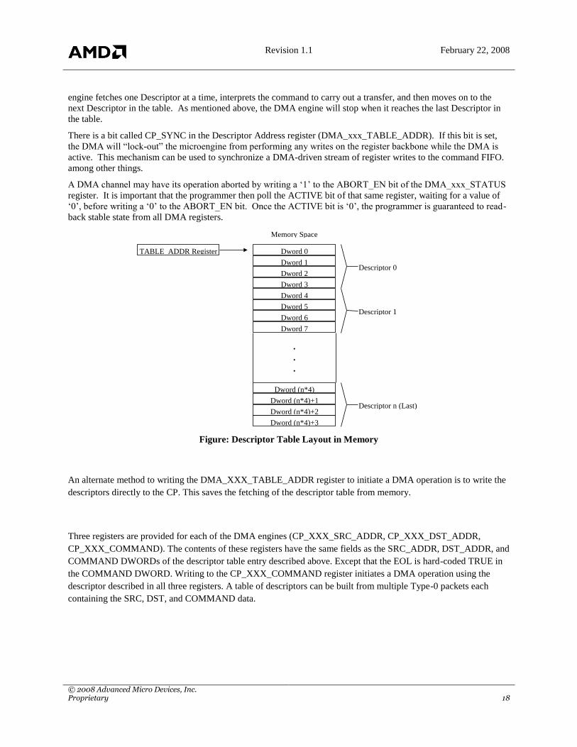
Multiple Descriptors may be stored contiguously in memory to make up a Descriptor Table (DT) (see Figure). The
last Descriptor in the Descriptor Table must be marked as such so that the DMA engine knows when to stop
consuming commands.
The programmer provides the DMA engine with a pointer to the beginning of the Descriptor Table, and the DMA
Revision 1.1 February 22, 2008
© 2008 Advanced Micro Devices, Inc. Proprietary 18
engine fetches one Descriptor at a time, interprets the command to carry out a transfer, and then moves on to the
next Descriptor in the table. As mentioned above, the DMA engine will stop when it reaches the last Descriptor in
the table.
There is a bit called CP_SYNC in the Descriptor Address register (DMA_xxx_TABLE_ADDR). If this bit is set,
the DMA will “lock-out” the microengine from performing any writes on the register backbone while the DMA is
active. This mechanism can be used to synchronize a DMA-driven stream of register writes to the command FIFO.
among other things.
A DMA channel may have its operation aborted by writing a „1‟ to the ABORT_EN bit of the DMA_xxx_STATUS
register. It is important that the programmer then poll the ACTIVE bit of that same register, waiting for a value of
„0‟, before writing a „0‟ to the ABORT_EN bit. Once the ACTIVE bit is „0‟, the programmer is guaranteed to read-
back stable state from all DMA registers.
Descriptor 0
Memory Space
Dword 0
Dword 1
Dword 2
Dword 3
TABLE_ADDR Register
Descriptor 1
Dword 4
Dword 5
Dword 6
Dword 7
Descriptor n (Last)
Dword (n*4)
Dword (n*4)+1
Dword (n*4)+2
Dword (n*4)+3
.
.
.
Figure: Descriptor Table Layout in Memory
An alternate method to writing the DMA_XXX_TABLE_ADDR register to initiate a DMA operation is to write the
descriptors directly to the CP. This saves the fetching of the descriptor table from memory.
Three registers are provided for each of the DMA engines (CP_XXX_SRC_ADDR, CP_XXX_DST_ADDR,
CP_XXX_COMMAND). The contents of these registers have the same fields as the SRC_ADDR, DST_ADDR, and
COMMAND DWORDs of the descriptor table entry described above. Except that the EOL is hard-coded TRUE in
the COMMAND DWORD. Writing to the CP_XXX_COMMAND register initiates a DMA operation using the
descriptor described in all three registers. A table of descriptors can be built from multiple Type-0 packets each
containing the SRC, DST, and COMMAND data.

Revision 1.1 February 22, 2008
© 2008 Advanced Micro Devices, Inc. Proprietary 19
4.8 Resetting the Command Processor
To support recovery from a power-down state the read pointer (CP_RB_RPTR) is writable. The read pointer is
initialized by writing the writable read pointer (CP_RB_RPTR_WR). Then, when the write pointer
(CP_RB_WPTR) is subsequently written the contents of the writable read pointer (CP_RB_RPTR_WR) are
transferred to the active read pointer (CP_RB_RPTR). As a precaution, an enable bit must be set in the control
register (CP_RB_CNTL) to allow the contents to transfer to the active read pointer (CP_RB_RPTR). Note that the
read pointer still resets to zero to ensure starting at the beginning of the buffer if the host does not initialize the
writable read pointer (CP_RB_RPTR_WR).
Therefore, a certain sequence of actions is required of the host in order to perform a “clean” soft reset of the CP:
1) Write CP_CSQ_CNTL and CP_CSQ_MODE to zero, effectively disabling the CP.
2) Write to the proper RBBM register to assert and then de-assert the Soft Reset signal to the CP.
3) Set the RB_RPTR_WR_ENA bit to enable writing of the RPTR if desired not to start from the
beginning of the buffer.
4) Write the CP_RB_RPTR_WR register if it is desired not to start at the beginning of the buffer.
5) Write CP_RB_WPTR, to make it match the RPTR, causing the ring buffer to appear to be empty.
6) Clear the RB_RPTR_WR_ENA bit if no further writes of the RPTR are desired.
7) Write CP_CSQ_CNTL or CP_CSQ_MODE to set the mode back to whatever you want.
4.9 Command Stream Synchronization
In the RBBM, there is an event engine that can be used to synchronize the sending of transactions to the Register
Backbone based on status signals from its clients. The CP however has a mechanism that can directly provide the
Host with knowledge of command status. This mechanism is the eight “SCRATCH” registers and their associated
functionality.
Associated with the eight “SCRATCH” registers in the CP are a scratch address register and a write mask. When a
scratch register is written, the CP will subsequently write its value to a location equal to what is programmed in the
SCRATCH_ADDR register plus the number (0 to 7) of the scratch register. The writing of the scratch register‟s
value by the CP is qualified by the register‟s write mask (SCRATCH_UMSK).
So, at the end of processing an Indirect Buffer, for example, a Type-0 packet can be inserted that writes a data
pattern to SCRATCH_REG1. The driver software can poll the external location SCRATCH_ADDR+1 and when it
changes to the value that was inserted in the Type-0 packet, the Driver will “know” that the CP has completed
parsing the indirect buffer up to that point. Note that this status only indicates that the CP is done to that point, the
data still may be being used by the rest of the pipeline.
Revision 1.1 February 22, 2008
© 2008 Advanced Micro Devices, Inc. Proprietary 20
For R5xx an interrupt is added associated with the scratch registers, which is asserted when the scratch register pair
selected is written to memory and is greater than or equal to the pair of values written by the Driver.
The CP can receive sync pulses from the back-end of the pipeline (CBA_CP_SYNC, CBB_CP_SYNC,
CBC_CP_SYNC, and CBD_CP_SYNC). When a pulse from each is received (pulse pair), the CP will write the
targeted scratch register with the corresponding CP_RESYNC_DATA value. The targeted scratch register is
determined by the 3-bit CP_RESYNC_ADDR which is a scratch register offset from the SCRATCH_ADDR base
address.
Because this function uses the SCRATCH_ADDR and SCRATCH_UMSK values, they must be initialized prior to
its use. The CP_RESYNC_ADDR and CP_RESYNC_DATA registers must also be programmed with the target
scratch register offset and the appropriate data respectively before the pulses are received. Both the
CP_RESYNC_ADDR and CP_RESYNC_DATA values are written into 8-deep FIFOs so that multiple
synchronization events can be en-queued in the CP.
If the sync pulses from the CB are asserted before programming the CP_RESYNC_ADDR and
CP_RESYNC_DATA, the logic will still work providing that Dynamic Clocking for the CP is disabled. Receipt of
the sync pulses by the CP does not cause the clocks to be enabled to the CP, so knowledge of these pulses may not
be remembered if Dynamic Clocking is enabled. Writing the CP_RESYNC_ADDR and CP_RESYNC_DATA
registers does enable the clocks to the CP. The “busy” signal to the CG will remain asserted as long as there is
RESYNC data in the ADDR and DATA FIFOs – keeping the clock enabled to the CP.
4.10 Starting the Indirect Streams
A write to the CP_IB_BUFSZ register triggers the Command Processor to start fetching the command stream from
the Indirect1 buffer, instead of from the Primary buffer. The CP will continue to fetch from the Indirect1 buffer,
starting at the address in the CP_IB_BASE register, and continuing until the CP_IB_BUFSZ amount is exhausted.
Then it will switch back to the Primary stream.
A write to the CP_IB2_BUFSZ register triggers the Command Processor to start fetching the command stream from
the Indirect2 buffer, instead of from the Indirect1 buffer. The CP will continue to fetch from the Indirect2 buffer,
starting at the address in the CP_IB2_BASE register, and continuing until the CP_IB2_BUFSZ amount is exhausted.
Then it will switch back to the Indirect1 stream.
Note that there are some important rules to follow when starting an indirect stream. Firstly, the write to the
CP_IB_BUFSZ or CP_IB2_BUFSZ register must be the last register-write of a Type 0 or Type 1 packet. The very
next packet that is delivered to the Command Stream Interpreter is the first packet of the respective indirect buffer.
The second rule is that the respective CP_IB_BASE or CP_IB2_BASE register must have been setup with the
proper value before the appropriate CP_IB_BUFSZ or CP_IB_BUFSZ register is written.
In PIO mode, the BUFSZ register still needs to be written with the size of the indirect buffer. Care must be taken to
write this register before the command queue fills in the CP.

Revision 1.1 February 22, 2008
© 2008 Advanced Micro Devices, Inc. Proprietary 21
4.11 Writing Host Data to the Command Stream Queue
Either or all of the Primary, Indirect1 and Indirect2 streams can be delivered to the Command Processor via host-
programmed writes to the Graphics Controller device. There is a range of register-space addresses assigned to each
of the three streams, that is, one aperture for the Primary Stream, one for the Indirect1 Stream, and one for the
Indirect2 Stream. The act of writing to a location in the aperture causes that data to be enqueued to the Command
Stream Queue. Note that the actual address of the written data is inconsequential; the data will be enqueued into the
Command Stream Queue in the order in which it was received from the host.
Note that each of the three streams can be in one of three delivery modes, resulting in nine possible combinations.
The three modes are:
1) OFF: The stream is disabled.
2) PUSH: The host is writing the stream data to the Command Processor. (also known as Programmed
I/O, or PIO mode)
3) PULL: The Command Processor is actively fetching the command stream from memory. (also known
as Bus Master, or BM mode)
Note that the BUFSZ register must be written to initiate indirect buffer parsing in the “PUSH” mode.

Revision 1.1 February 22, 2008
© 2008 Advanced Micro Devices, Inc. Proprietary 22
4.12 Writing to the MicroEngine RAM
In order to change a location in the MicroEngine RAM, first load the CP_ME_RAM_ADDR Register with the
address of the RAM into which data is to be written. Next, the host performs two writes; the first must be to the
CP_ME_RAM_DATAH port, and the second to the CP_ME_RAM_DATAL port. Internally, the Command
Processor maintains a 40-bit holding registers which concatenates the lower 8-bits of the DATAH value to the top of
the 32-bit DATAL value, and at the end of the write of the DATAL value, the 40-bit value is written to the RAM at
the location specified by the RAM Address Register. The RAM Address Register is then auto-incremented to point
to the next location in the RAM. This process of writing two data values may be repeated to write to successive
RAM locations without re-loading the RAM Address Register.
4.13 Reading from the MicroEngine RAM
In order to read a location in the MicroEngine RAM, first load the CP_ME_RAM_RADDR Register with the
address of the RAM from which data is to be read. This write triggers the Command Processor to read the 40-bit
data value at that RAM location and transfer it to an internal 40-bit holding register. Also, the RAM Address
Register is auto-incremented to point to the next location in the RAM. Next, the host performs two read cycles, the
first from the DATAH port, and the second from the DATAL port. At the end of the DATAL cycle, the next
location of the RAM is transferred to the 40-bit holding register, and the RAM Address Register is again auto-
incremented. This process of reading two values may be repeated to read from successive RAM locations without
re-loading the RAM Address Register.

Revision 1.1 February 22, 2008
© 2008 Advanced Micro Devices, Inc. Proprietary 23
4.14 Starting a DMA Operation
There are two methods to initiate a DMA operation – Descriptor Tables or Direct Descriptor Entry Register Writes.
To program a DMA operation via Descriptor Tables, the programmer has to build the table in the frame buffer first,
being sure to mark the last entry of the list as “End Of List”. Then, the programmer can write the starting address of
the descriptor table into the Descriptor Table Address Queue (DTAQ) through the xxx_DMA_TABLE_ADDR port.
The action of writing the first starting address into the DTAQ will trigger the DMA operation.
The type of transfer operation depends on the DMA_COMMAND DWORD in the Descriptor. It controls such
variables as: the length of the transfer, whether the Source/Destination addresses are in memory-space or register-
space, whether the Source/Destination addresses auto-increment with each transfer, and whether an interrupt is
generated when the entire Descriptor Table has been processed.
The second method - Direct Descriptor Entry Register Writes – involves writing the three DMA Entry registers.
Three registers are provided for each of the DMA engines (CP_XXX_SRC_ADDR, CP_XXX_DST_ADDR,
CP_XXX_COMMAND). The contents of these registers have the same fields as the SRC_ADDR, DST_ADDR, and
COMMAND DWORDs of the descriptor table entry. Except that the EOL is hard-coded TRUE in the COMMAND
DWORD. Writing to the CP_XXX_COMMAND register initiates a DMA operation using the descriptor described
in all three registers. A table of descriptors can be built from multiple Type-0 packets each containing the SRC,
DST, and COMMAND data.

Revision 1.1 February 22, 2008
© 2008 Advanced Micro Devices, Inc. Proprietary 24
5. PM4
5.1 Packet Types
When programming in the PM4 mode, we do not need to write directly to registers to carry out drawing operations
on the screen. Instead, what we need to do is to prepare data in the format of PM4 Command Packets in the system
memory, and let the hardware (Microengine) to do the rest of the job.
Four types of PM4 command packets are currently defined. They are types 0, 1, 2 and 3 as shown in the following
figure. A PM4 command packet consists of a packet header, identified by field HEADER, and an information body,
identified by IT_BODY, that follows the header. The packet header defines the operations to be carried out by the
PM4 micro-engine, and the information body contains the data to be used by the engine in carrying out the
operation. In the following, we use brackets [.] to denote a 32-bit field (referred to as DWORD) in a packet, and
braces {.} to denote a size-varying field that may consist of a number of DWORDs. If a DWORD is shared by more
than one field, the fields are separated by „|‟. The field that appears on the far left takes the most significant bits, and
the field that appears on the far right takes the least significant bits. For example, DWORD [HI_WORD |
LO_WORD] denotes that HI_WORD is defined on bits 16-31, and LO_WORD on bits 0-15. A C-style notation of
referencing an element of a structure is used to refer to a subfield of a main field. For example,
MAIN_FIELD.SUBFIELD refers to the subfield SUBFIELD of MAIN_FIELD.
Bit position 63
1
3
0
2
9
2
8
2
7
2
6
2
5
2
4
2
3
2
2
2
1
2
0
1
9
1
8
1
7
1
6
1
5
1
4
1
3
1
2
1
1
1
09 8 7 5 4 3 2 1 0
00 COUNT a BASE_INDEX
REG_DATA_1
REG_DATA_2
Packet header
IT_BODY...
REG_DATA_n
Type-0 packet
Type-1 packet
01 Reserved REG_INDEX2 REG_INDEX1
REG_DATA_1
REG_DATA_2
Packet header
Bit position 63
1
3
0
2
9
2
8
2
7
2
6
2
5
2
4
2
3
2
2
2
1
2
0
1
9
1
8
1
7
1
6
1
5
1
4
1
3
1
2
1
1
1
09 8 7 5 4 3 2 1 0
IT_BODY
Revision 1.1 February 22, 2008
© 2008 Advanced Micro Devices, Inc. Proprietary 25
10 ReservedPacket header
Bit position 63
1
3
0
2
9
2
8
2
7
2
6
2
5
2
4
2
3
2
2
2
1
2
0
1
9
1
8
1
7
1
6
1
5
1
4
1
3
1
2
1
1
1
09 8 7 5 4 3 2 1 0
Type-2 packet
11 COUNT IT_OPCODE Reserved
DATA_1
Packet header
Bit position 63
1
3
0
2
9
2
8
2
7
2
6
2
5
2
4
2
3
2
2
2
1
2
0
1
9
1
8
1
7
1
6
1
5
1
4
1
3
1
2
1
1
1
09 8 7 5 4 3 2 1 0
IT_BODY
Type-3 packet
DATA_2
...
Data_n
5.1.1 Type-0 Packet
Functionality
Write N DWORDs in the information body to the N consecutive registers, or to the register, pointed to by the
BASE_INDEX field of the packet header.
Format
Ordinal Field Name
1 [ HEADER ]
2 [REG_DATA_1]
3 [REG_DATA_2]
...
N+1 [REG_DATA_N]
Header Fields
Bit(s) Field Name Description
12:0 BASE_INDEX The BASE_INDEX[12:0] correspond to byte address bits [14:2]. So the
BASE_INDEX is the DWORD Memory-mapped address.
The BASE_INDEX field width supports up to DWORD address: 0x7FFF.
14:13 Reserved Reserved for future expansion of address space.
15 ONE_REG_WR 0:- Write the data to N consecutive registers.
1:- Write all the data to the same register.
29:16 COUNT Count of DWORDs in the information body. Its value should be N-1 if there
are N DWORDs in the information body.
31:30 TYPE Packet identifier. It should be zero.
Note: Symbol „:-‟ reads “defined as.”
Information Body

Revision 1.1 February 22, 2008
© 2008 Advanced Micro Devices, Inc. Proprietary 26
Bit(s) Field Name Description
31:0 REG_DATA _x The bits correspond to those defined for the relevant register. Note the suffix x
of REG_DATA_x stands for an integer ranging from 1 to N.
Comment
The use of this packet requires the complete understanding of the registers to be written.
5.1.2 Type-1 Packet
Functionality
Write REG_DATA_1 and REG_DATA_2 in the information body respectively to the registers pointed to by
REG_INDEX1 and REG_INDEX2. Note that this packet cannot address the entire address space. It is recommended
that Type 0 packets be used instead.
Format
Ordinal Field Name
1 [ HEADER ]
2 [REG_DATA_1]
3 [REG_DATA_2]
Header fields
Bit(s) Field Name Description
10:0 REG_INDEX1 The field points to a memory-mapped register that REG_DATA_1 is written to.
21:11 REG_INDEX2 The field points to a memory-mapped register that REG_DATA_2 is written to.
29:22 Reserved
31:30 TYPE Packet identifier. It should be 1 (one).
Information Body
Bit(s) Field Name Description
31:0 REG_DATA_x The bits correspond to those defined for the relevant register.
5.1.3 Type-2 Packet
Functionality
This is a filler packet. It has only the header, and its content is not important except for bits 30 and 31. It is used to
fill up the trailing space left when the allocated buffer for a packet, or packets, is not fully filled. This allows the
microengine to skip the trailing space and to fetch the next packet.
Format
Ordinal Field Name
1 [ HEADER ]
Header fields
Bit(s) Field Name Description
29:0 reserved

Revision 1.1 February 22, 2008
© 2008 Advanced Micro Devices, Inc. Proprietary 27
31:30 TYPE Packet identifier. It should be 2.
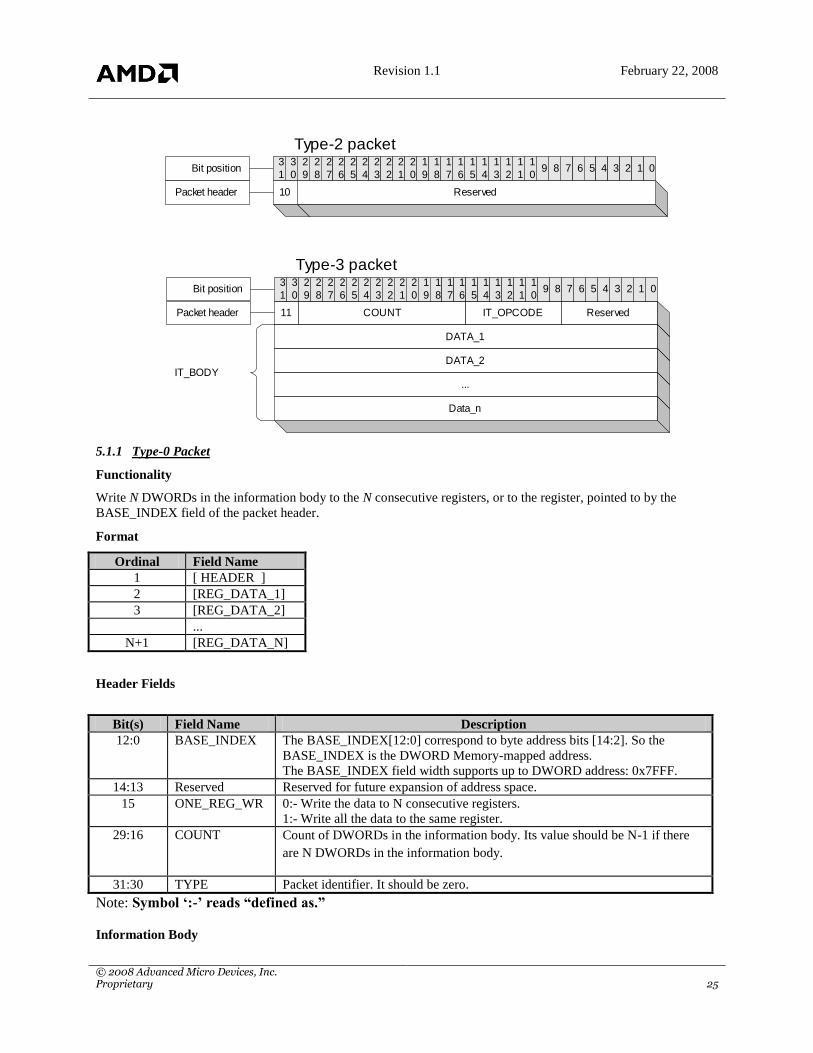
5.1.4 Type-3 Packet
Functionality
Carry out the operation indicated by field IT_OPCODE.
Format
Ordinal Field Name
1 [ HEADER ]
2 {IT_BODY}
Header fields
Bit(s) Field Name Description
7:0 Reserved This field is undefined, and is set to zero by default.
15:8 IT_OPCODE Operation to be carried out. See section B.2 for details.
29:16 COUNT Number of DWORDs -1 in the information body. It is N-1 if the information body
contains N DWORDs.
31:30 TYPE Packet identifier. It should be 3.
Information Body
The information body IT_BODY will be described extensively in the following section.

Revision 1.1 February 22, 2008
© 2008 Advanced Micro Devices, Inc. Proprietary 28
5.2 Definition of Type-3 packets
Type-3 packets has a common format in their headers. However, the size of their information body may vary
depending on the value of field IT_OPCODE. The size of the information body is indicated by field COUNT. If the
size of the information is N DWORDs, the value of COUNT is N-1. In the following packet definitions, we will
describe the field IT_BODY for each packet with respect to a given IT_OPCODE, and omit the header. The MSB
of the IT_OPCODE identifies whether this packet requires the GUI_CONTROL field (described later). A 1 in the
MSB of the IT_OPCODE indicates that GUI control is required. A 0 in the MSB of the IT_OPCODE indicates that
the GUI_CONTROL should be omitted.
Revision 1.1 February 22, 2008
© 2008 Advanced Micro Devices, Inc. Proprietary 29
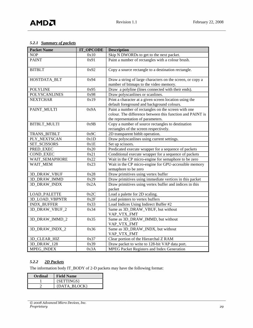
5.2.1 Summary of packets
Packet Name IT_OPCODE Description
NOP 0x10 Skip N DWORDs to get to the next packet.
PAINT 0x91
Paint a number of rectangles with a colour brush.
BITBLT
0x92
Copy a source rectangle to a destination rectangle.
HOSTDATA_BLT 0x94 Draw a string of large characters on the screen, or copy a
number of bitmaps to the video memory.
POLYLINE 0x95 Draw a polyline (lines connected with their ends).
POLYSCANLINES 0x98 Draw polyscanlines or scanlines.
NEXTCHAR 0x19
Print a character at a given screen location using the
default foreground and background colours.
PAINT_MULTI 0x9A Paint a number of rectangles on the screen with one
colour. The difference between this function and PAINT is
the representation of parameters.
BITBLT_MULTI 0x9B Copy a number of source rectangles to destination
rectangles of the screen respectively.
TRANS_BITBLT 0x9C 2D transparent bitblt operation.
PLY_NEXTSCAN 0x1D Draw polyscanlines using current settings.
SET_SCISSORS 0x1E Set up scissors.
PRED_EXEC 0x20 Predicated execute wrapper for a sequence of packets
COND_EXEC 0x21 Conditional execute wrapper for a sequence of packets
WAIT_SEMAPHORE 0x22 Wait in the CP micro-engine for semaphore to be zero
WAIT_MEM 0x23 Wait in the CP micro-engine for GPU-accessible memory
semaphore to be zero
3D_DRAW_VBUF 0x28 Draw primitives using vertex buffer
3D_DRAW_IMMD 0x29 Draw primitives using immediate vertices in this packet
3D_DRAW_INDX 0x2A Draw primitives using vertex buffer and indices in this
packet
LOAD_PALETTE 0x2C Load a palette for 2D scaling.
3D_LOAD_VBPNTR 0x2F Load pointers to vertex buffers
INDX_BUFFER 0x33 Load Indices Using Indirect Buffer #2
3D_DRAW_VBUF_2 0x34 Same as 3D_DRAW_VBUF, but without
VAP_VTX_FMT
3D_DRAW_IMMD_2 0x35 Same as 3D_DRAW_IMMD, but without
VAP_VTX_FMT
3D_DRAW_INDX_2 0x36 Same as 3D_DRAW_INDX, but without
VAP_VTX_FMT
3D_CLEAR_HIZ 0x37 Clear portion of the Hierarchal Z RAM
3D_DRAW_128 0x39 Draw packet to write to 128-bit VAP data port.
MPEG_INDEX 0x3A MPEG Packet Registers and Index Generation
5.2.2 2D Packets
The information body IT_BODY of 2-D packets may have the following format:
Ordinal Field Name
1 {SETTINGS}
2 {DATA_BLOCK}

Revision 1.1 February 22, 2008
© 2008 Advanced Micro Devices, Inc. Proprietary 30
SETTINGS
This field consists of 2 subfields, GUI_CONTROL and SETUP_BODY.
Ordinal Field Name
1 [ GUI_CONTROL ]
2 {SETUP_BODY}
SETTINGS.GUI_CONTROL
This field will be used to setup the register DP_GUI_MASTER_CNTL, and it also decides the content of
SETTINGS.SETUP_BODY.
Bit(s) Field Name Description Status
0 SRC_PITCH_OFF The bit controls the pitch and offset of the blitting source.
0:- Use the default pitch and offset, and no datum
[SRC_PITCH_OFFSET] is supplied in SETUP_BODY.
1:- Use the datum [SRC_PITCH_OFFSET] supplied in SETUP_BODY
to set up a new pitch offset.
1 DST_PITCH_OFF The bit controls the pitch and offset of the blitting destination.
0:- Use the default pitch and offset, and no datum
[DST_PITCH_OFFSET] is supplied in SETUP_BODY.
1:- Use the datum [DST_PITCH_OFFSET] supplied in SETUP_BODY.
The pitch may mean the bitmap pitch and the offset may points the off-
screen area of the video memory.
2 SRC_CLIPPING This bit controls the clipping parameters of the blitting source.
0:- Use the default clipping parameters, and no relevant clipping data
supplied in SETUP_BODY.
1:- Use datum [SRC_SC_BOT_RITE] supplied in SETUP_BODY to set
up the bottom and right edges of the clipping rectangle.
3 DST_CLIPPING This bit controls the clipping parameters of the blitting destination.
0:- Use the default clipping parameters, and no relevant clipping data
supplied in SETUP_BODY.
1:- Use data [SC_TOP_LEFT] and [SC_BOTTOM_RIGHT] supplied in
SETUP_BODY to set up a new clipping rectangle.
7:4 BRUSH_TYPE Types of brush used in drawing. The type code determines how to supply
data to the subfield BRUSH_PACKET in SETUP_BODY. See detailed
definition of BRUSH_TYPE in the following.
11:8 DST_TYPE
{Not Used by uCode}
The pixel type of the destination.
0--1 :- (reserved)
2 :- 8 bpp pseudocolor
3 :- 16 bpp aRGB 1555
4 :- 16 bpp RGB 565
5 :- reserved
6 :- 32 bpp aRGB 8888
7 :- 8 bpp RGB 332
8 :- Y8 greyscale
9 :- RGB8 greyscale (8 bit intensity, duplicated for all 3 channels. Green
channel is used on writes)
10 :- (reserved)
11 :- YUV 422 packed (VYUY)
12 :- YUV 422 packed (YVYU)
13 :- (reserved)
7 through 15
not supported in
3D pipe
Revision 1.1 February 22, 2008
© 2008 Advanced Micro Devices, Inc. Proprietary 31
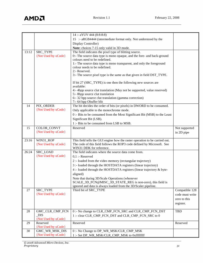
14 :- aYUV 444 (8:8:8:8)
15 :- aRGB4444 (intermediate format only. Not understood by the
Display Controller)
Note: choices 7-15 only valid in 3D mode.
13:12 SRC_TYPE
{Not Used by uCode}
The field indicates the pixel type of blitting source.
0:- The source data type is mono opaque, and the fore- and back-ground
colours need to be redefined.
1:- The source data type is mono transparent, and only the foreground
colour needs to be redefined.
2:- Reserved.
3:- The source pixel type is the same as that given in field DST_TYPE.
If bit 27 (SRC_TYPE) is one then the following new sources are
available:
4:- 4bpp source clut translation (May not be supported, value reserved)
5:- 8bpp source clut translation
6:- 32 bpp source clut translation (gamma correction)
7:- 64 bpp Obuffer blit
14 PIX_ORDER
{Not Used by uCode} The bit decides the order of bits (or pixels) in DWORD to be consumed.
Only applicable to the monochrome mode.
0 :- Bits to be consumed from the Most Significant Bit (MSB) to the Least
Significant Bit (LSB).
1 :- Bits to be consumed from LSB to MSB.
15 COLOR_CONVT
{Not Used by uCode}
Reserved Not supported
in 2D pipe
23:16 WIN31_ROP
{Not Used by uCode}
This field tells the GUI engine how the raster operation to be carried out.
The code of this field follows the ROP3 code defined by Microsoft. See
WIN31 DDK for reference.
26:24 SRC_LOAD
{Not Used by uCode}
The field indicates where the source data come from.
0,1 :- Reserved
2 :- loaded from the video memory (rectangular trajectory)
3 :- loaded through the HOSTDATA registers (linear trajectory)
4 :- loaded through the HOSTDATA registers (linear trajectory & byte-
aligned)
Note that during 3D/Scale Operations (whenever
SCALE_3D_FCN@MISC_3D_STATE_REG is non-zero), this field is
ignored and data is always loaded from the 3D/Scaler pipeline.
27 SRC_TYPE
{Not Used by uCode}
Third bit of SRC_TYPE Compatible 128
code must write
zero to this
register.
28 GMC_CLR_CMP_FCN
_DIS
{Not Used by uCode}
0 :- No change to CLR_CMP_FCN_SRC and CLR_CMP_FCN_DST
1 :- clear CLR_CMP_FCN_DST and CLR_CMP_FCN_SRC to 0
TBD
29 Reserved
{Not Used by uCode}
Reserved Reserved
30 GMC_WR_MSK_DIS
{Not Used by uCode}
0 :- No Change to DP_WR_MSK/CLR_CMP_MSK
1 :- Set DP_WR_MSK/CLR_CMP_MSK to 0xffffffff

Revision 1.1 February 22, 2008
© 2008 Advanced Micro Devices, Inc. Proprietary 32
31 BRUSH_FLAG This field indicates whether there is a field BRUSH_Y_X field in the
SETTINGS.SETUP_BODY.
0:- No such a field in SETTINGS.SETUP_BODY.
1:- There is a field in SETTINGS.SETUP_BODY.
SETTINGS.SETUP_BODY
This field may contain the following subfields. Their presence depends on the bits 0-7 of SETTINGS.GUI_CONTROL.
Ordinal Field Name Description
1 [SRC_PITCH_OFFSET] Bit 30: Select between untiled(0) and tiled (1)
Bit 31: select between no microtiling(0) and microtiling(1)
Bits 29:22 Pitch in units of 64 bytes, 64 to 16384 bytes across
bits 21:0 Offset in units of 1KB, 0 to 4GB-1K
2 [DST_PITCH_OFFSET] Bit 30: Select between untiled(0) and tiled (1)
Bit 31: select between no microtiling(0) and microtiling(1)
Bits 29:22 Pitch in units of 64 bytes, 64 to 16384 bytes across
bits 21:0 Offset in units of 1KB, 0 to 4GB-1K
3 [SRC_SC_BOT_RITE] The parameters are used to setup the clipping area of the source.
The implied coordinates of the top-left corner of the clipping
rectangle is the same as the source.
[13:0] :- x-coordinate of the right edge of the clipping rectangle (in
number of pixels).
[29:16] :- y-coordinate of the bottom edge of the clipping
rectangle (in number of scanlines).
4 [SC_TOP_LEFT]
[SC_BOT_RITE]
The parameters are used to setup the clipping area of destination.
SC_TOP_LEFT:
[13:0] :- x-coordinate of the left edge of the clipping rectangle (in
number of pixels).
[29:16] :- y-coordinate of the top edge of the clipping rectangle (in
number of scanlines).
SC_BOT_RITE:
[13:0] :- x-coordinate of the right edge of the clipping rectangle (in
number of pixels).
[29:16] :- y-coordinate of the bottom edge of the clipping
rectangle (in number of scanlines).
5 { BRUSH_PACKET } The content of this field is determined by field
SETTINGS.GUI_CONTROL.BRUSH_TYPE. See the following
table for the possible content.
6 [BRUSH_Y_X] [4:0] :- x-coordinate for brush alignment.
[12:8] :- y-coordinate for brush alignment.
[20:16] :- Initial value used for BRUSH_X pointer in drawing
Lines. When POLY_LINE is off, it is reloaded from BRUSH_X
at the end of the line. When POLY_LINE is on, it is reloaded
from the current Brush pointer at the end of the line. Whenever
BRUSH_X is updated, the field should be written with the same
value.
SETTINGS.SETUP_BODY.BRUSH_PACKET
Revision 1.1 February 22, 2008
© 2008 Advanced Micro Devices, Inc. Proprietary 33
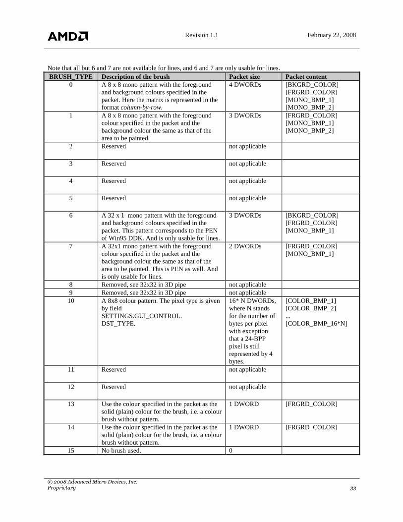
Note that all but 6 and 7 are not available for lines, and 6 and 7 are only usable for lines.
BRUSH_TYPE Description of the brush Packet size Packet content
0 A 8 x 8 mono pattern with the foreground
and background colours specified in the
packet. Here the matrix is represented in the
format column-by-row.
4 DWORDs [BKGRD_COLOR]
[FRGRD_COLOR]
[MONO_BMP_1]
[MONO_BMP_2]
1 A 8 x 8 mono pattern with the foreground
colour specified in the packet and the
background colour the same as that of the
area to be painted.
3 DWORDs [FRGRD_COLOR]
[MONO_BMP_1]
[MONO_BMP_2]
2 Reserved not applicable
3 Reserved not applicable
4 Reserved not applicable
5 Reserved not applicable
6 A 32 x 1 mono pattern with the foreground
and background colours specified in the
packet. This pattern corresponds to the PEN
of Win95 DDK. And is only usable for lines.
3 DWORDs [BKGRD_COLOR]
[FRGRD_COLOR]
[MONO_BMP_1]
7 A 32x1 mono pattern with the foreground
colour specified in the packet and the
background colour the same as that of the
area to be painted. This is PEN as well. And
is only usable for lines.
2 DWORDs [FRGRD_COLOR]
[MONO_BMP_1]
8 Removed, see 32x32 in 3D pipe not applicable
9 Removed, see 32x32 in 3D pipe not applicable
10 A 8x8 colour pattern. The pixel type is given
by field
SETTINGS.GUI_CONTROL.
DST_TYPE.
16* N DWORDs,
where N stands
for the number of
bytes per pixel
with exception
that a 24-BPP
pixel is still
represented by 4
bytes.
[COLOR_BMP_1]
[COLOR_BMP_2]
...
[COLOR_BMP_16*N]
11 Reserved not applicable
12 Reserved not applicable
13 Use the colour specified in the packet as the
solid (plain) colour for the brush, i.e. a colour
brush without pattern.
1 DWORD [FRGRD_COLOR]
14 Use the colour specified in the packet as the
solid (plain) colour for the brush, i.e. a colour
brush without pattern.
1 DWORD [FRGRD_COLOR]
15 No brush used. 0

Revision 1.1 February 22, 2008
© 2008 Advanced Micro Devices, Inc. Proprietary 34
Brush packet content
Field Name Description
[FRGRD_COLOR] The foreground colour of the text in the RGBQUAD format.
bits [7:0] :- intensity of Blue;
bits [15:8] :- intensity of Green; and
bits [23:16] :- intensity of Red.
bits [31:25] :- reserved.
[BKGRD_COLOR] The background colour of the text in the RGBQUAD format.
bits [7:0] :- intensity of Blue;
bits [15:8] :- intensity of Green; and
bits [23:16] :- intensity of Red.
bits [31:25] :- reserved.
[MONO_BMP_x] Raster data of monochrome pixels. One bit represents one pixel. If the
number of pixels for the field is less than 32, the pixels take the lower bits.
The remaining bits should be filled with 0‟s.
[COLOR_BMP_x] Raster data of colour pixels. The representation depends on the pixel type.
DATA_BLOCK
The composition of this field depends on the operation code IT_OPCODE given in the header. Section B.2 gives
details of DATA_BLOCK with respect to IT_OPCODE. In the following, the field SETTINGS may appear in the
definition of a packet, but will not be described further.
5.2.2.1 NOP
Functionality
Skip a number of DWORDs to get to the next packet.
Format
Ordinal Field Name
1 [ HEADER ]
2 {DATA_BLOCK}
DATA_BLOCK
This field may consist of a number of DWORDs, and the content may be anything.
5.2.2.2 PAINT
Functionality
Paint a number of rectangles with a colour brush.
Format
Ordinal Field Name
1 [ HEADER ]
2 {SETTINGS}
3 {DATA_BLOCK}
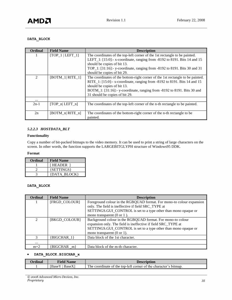
Revision 1.1 February 22, 2008
© 2008 Advanced Micro Devices, Inc. Proprietary 35
DATA_BLOCK
Ordinal Field Name Description
1 [TOP_1 | LEFT_1] The coordinates of the top-left corner of the 1st rectangle to be painted.
LEFT_1: [15:0]:- x-coordinate, ranging from -8192 to 8191. Bits 14 and 15
should be copies of bit 13.
TOP_1: [31:16]:- y-coordinate, ranging from -8192 to 8191. Bits 30 and 31
should be copies of bit 29.
2 [BOTM_1| RITE_1] The coordinates of the bottom-right corner of the 1st rectangle to be painted.
RITE_1: [15:0]:- x-coordinate, ranging from -8192 to 8191. Bits 14 and 15
should be copies of bit 13.
BOTM_1: [31:16]:- y-coordinate, ranging from -8192 to 8191. Bits 30 and
31 should be copies of bit 29.
...
2n-1 [TOP_n| LEFT_n] The coordinates of the top-left corner of the n-th rectangle to be painted.
2n [BOTM_n| RITE_n] The coordinates of the bottom-right corner of the n-th rectangle to be
painted.
5.2.2.3 HOSTDATA_BLT
Functionality
Copy a number of bit-packed bitmaps to the video memory. It can be used to print a string of large characters on the
screen. In other words, the function supports the LARGEBITGLYPH structure of Windows95 DDK.
Format
Ordinal Field Name
1 [ HEADER ]
2 {SETTINGS}
3 {DATA_BLOCK}
DATA_BLOCK
Ordinal Field Name Description
1 [FRGD_COLOUR] Foreground colour in the RGBQUAD format. For mono-to colour expansion
only. The field is ineffective if field SRC_TYPE at
SETTINGS.GUI_CONTROL is set to a type other than mono opaque or
mono transparent (0 or 1 ).
2 [BKGD_COLOUR] Background colour in the RGBQUAD format. For mono-to colour
expansion only. The field is ineffective if field SRC_TYPE at
SETTINGS.GUI_CONTROL is set to a type other than mono opaque or
mono transparent (0 or 1).
3 {BIGCHAR_1} Data block of the 1st character.
...
m+2 {BIGCHAR _m} Data block of the m-th character.
DATA_BLOCK.BIGCHAR_x
Ordinal Field Name Description
1 [BaseY | BaseX] The coordinate of the top-left corner of the character‟s bitmap.

Revision 1.1 February 22, 2008
© 2008 Advanced Micro Devices, Inc. Proprietary 36
BaseX: [15:0] :- x-coordinate.
BaseY: [31:16] :- y-coordinate.
2 [HEIGHT | WIDTH] The geometry of the bitmap.
WIDTH: [15:0] :- width of the bitmap.
HEIGHT: [31:16] :- height of the bitmap.
3 [ NUMBER[13:0] ] The number of DWORDs in the bitmap. It should be m in this case. The max
value is 0x3FFF.
4 [RASTER_1] The 1st DWORD of the mono bitmap data.
...
m+3 [RASTER_m ] The m-th DWORD of the mono bitmap data.
5.2.2.4 POLYLINE
Functionality
Draw a polyline specified by a set of coordinates ),( 00 yx , ),( 11 yx , ..., ),( nn yx , where coordinate ),( 00 yx is the
beginning of the polyline, and coordinate ),( nn yx is the end.
Format
Ordinal Field Name
1 [ HEADER ]
2 {SETTINGS}
3 {DATA_BLOCK}
DATA_BLOCK
Ordinal Field Name Description
1 [Y0 | X0] The starting coordinate of the polyline.
X0: [15:0] :- x-component of the coordinate. Y0: [31:16]:- y-component.
2 [Y1 | X1] The 2nd coordinate of the polyline. Definition of bits is the same as above.
...
n+1 [Yn | Xn] The ending coordinate of the polyline. Definition of bits is the same as
above.
5.2.2.5 POLYSCANLINES
Functionality
Draw a number of scanlines and polyscanlines. The number can be one. The difference between a scanline and a
polyscanline is that a scanline has only one starting x-coordinate and one ending x-coordinate while a polyscanline
has a number of starting-ending x-coordinate pairs.
Format
Ordinal Field Name
1 [ HEADER ]
2 {SETTINGS}

Revision 1.1 February 22, 2008
© 2008 Advanced Micro Devices, Inc. Proprietary 37
3 {DATA_BLOCK}
DATA_BLOCK
Ordinal Field Name Description
1 [SCAN_COUNT] The number of scan subpackets identified by SCAN_x, where x denotes the
ordinal number of a SCAN subpacket.
2 { SCAN_1 } The 1st scanline/polyscanline.
...
n+1 { SCAN_n } The n-th scanline/polyscanline.
DATA_BLOCK.SCAN_x
Ordinal Field Name Description
1 [ NUM_LINE[13:0] ] The number of line segments in a polyscanline. Maximum is 0x3fff.
2 [HEIGHT | TOP ] TOP: [15:0] :- y-coordinate of the polyscanline.
HEIGHT: [31:16] :- The thickness of the line measured in pixels.
3 [END_1 | START_1] START_1: [15:0] :- the starting x-coordinate of the 1st line segment.
END_1: [31:16]:- the ending x-coordinate of the 1st line segment.
...
n+2 [END_n |START_n] START_n: [15:0] :- the starting x-coordinate of the n-th line segment.
END_n: [31:16]:- the ending x-coordinate of the n-th line segment.
5.2.2.6 NEXTCHAR
Functionality
Print a character at a given screen location using the default foreground and background colours.
Format
Ordinal Field Name
1 [ HEADER ]
2 {DATA_BLOCK}
DATA_BLOCK
Ordinal Field Name Description
1 [DST_Y | DST_X] The coordinates of the top-left corner of the destination bitmap.
DST_X: [15:0]:- x-coordinate, ranging from -8192 to 8191. Bits 14 and 15
should be copies of bit 13.
DST_Y: [31:16]:- y-coordinate, ranging from -8192 to 8191. Bits 30 and 31
should be copies of bit 29.
2 [DST_H | DST_W] The width and height of the destination bitmap, expressed in unsigned
integers.
DST_W: [15:0]:- width. DST_H [31:16]:- height.
3 [BITMAP_DATA_1] The 1st DWORD of the bitmap data.
...
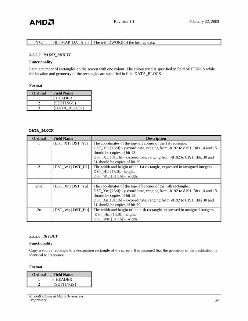
Revision 1.1 February 22, 2008
© 2008 Advanced Micro Devices, Inc. Proprietary 38
N+2 [BITMAP_DATA_n] The n-th DWORD of the bitmap data.
5.2.2.7 PAINT_MULTI
Functionality
Paint a number of rectangles on the screen with one colour. The colour used is specified in field SETTINGS while
the location and geometry of the rectangles are specified in field DATA_BLOCK.
Format
Ordinal Field Name
1 [ HEADER ]
2 {SETTINGS}
3 {DATA_BLOCK}
DATA_BLOCK
Ordinal Field Name Description
1 [DST_X1 | DST_Y1] The coordinates of the top-left corner of the 1st rectangle.
DST_Y1: [15:0]:- y-coordinate, ranging from -8192 to 8191. Bits 14 and 15
should be copies of bit 13.
DST_X1: [31:16]:- x-coordinate, ranging from -8192 to 8191. Bits 30 and
31 should be copies of bit 29.
2 [DST_W1 | DST_H1] The width and height of the 1st rectangle, expressed in unsigned integers.
DST_H1: [15:0]:- height.
DST_W1: [31:16]:- width.
...
2n-1 [DST_Xn | DST_Yn] The coordinates of the top-left corner of the n-th rectangle.
DST_Yn: [15:0]:- y-coordinate, ranging from -8192 to 8191. Bits 14 and 15
should be copies of bit 13.
DST_Xn: [31:16]:- x-coordinate, ranging from -8192 to 8191. Bits 30 and
31 should be copies of bit 29.
2n [DST_Wn | DST_Hn] The width and height of the n-th rectangle, expressed in unsigned integers.
DST_Hn: [15:0]:- height.
DST_Wn: [31:16]:- width.
5.2.2.8 BITBLT
Functionality
Copy a source rectangle to a destination rectangle of the screen. It is assumed that the geometry of the destination is
identical to its source.
Format
Ordinal Field Name
1 [ HEADER ]
2 {SETTINGS}
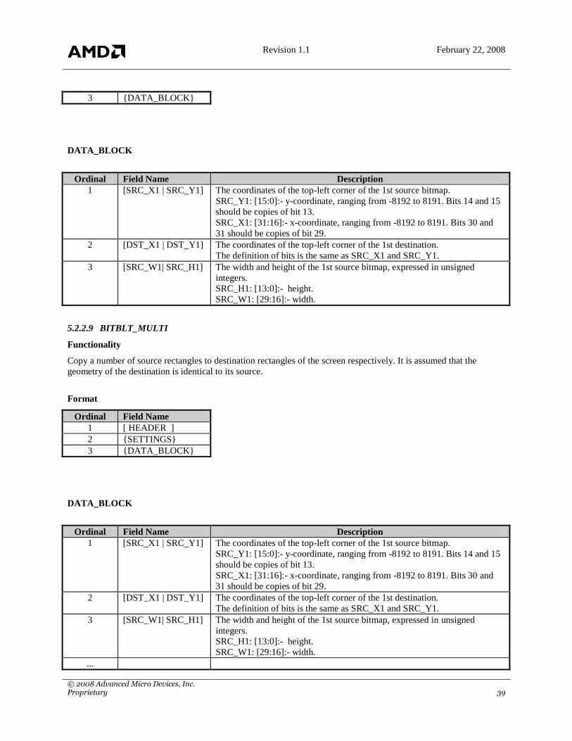
Revision 1.1 February 22, 2008
© 2008 Advanced Micro Devices, Inc. Proprietary 39
3 {DATA_BLOCK}
DATA_BLOCK
Ordinal Field Name Description
1 [SRC_X1 | SRC_Y1] The coordinates of the top-left corner of the 1st source bitmap.
SRC_Y1: [15:0]:- y-coordinate, ranging from -8192 to 8191. Bits 14 and 15
should be copies of bit 13.
SRC_X1: [31:16]:- x-coordinate, ranging from -8192 to 8191. Bits 30 and
31 should be copies of bit 29.
2 [DST_X1 | DST_Y1] The coordinates of the top-left corner of the 1st destination.
The definition of bits is the same as SRC_X1 and SRC_Y1.
3 [SRC_W1| SRC_H1] The width and height of the 1st source bitmap, expressed in unsigned
integers.
SRC_H1: [13:0]:- height.
SRC_W1: [29:16]:- width.
5.2.2.9 BITBLT_MULTI
Functionality
Copy a number of source rectangles to destination rectangles of the screen respectively. It is assumed that the
geometry of the destination is identical to its source.
Format
Ordinal Field Name
1 [ HEADER ]
2 {SETTINGS}
3 {DATA_BLOCK}
DATA_BLOCK
Ordinal Field Name Description
1 [SRC_X1 | SRC_Y1] The coordinates of the top-left corner of the 1st source bitmap.
SRC_Y1: [15:0]:- y-coordinate, ranging from -8192 to 8191. Bits 14 and 15
should be copies of bit 13.
SRC_X1: [31:16]:- x-coordinate, ranging from -8192 to 8191. Bits 30 and
31 should be copies of bit 29.
2 [DST_X1 | DST_Y1] The coordinates of the top-left corner of the 1st destination.
The definition of bits is the same as SRC_X1 and SRC_Y1.
3 [SRC_W1| SRC_H1] The width and height of the 1st source bitmap, expressed in unsigned
integers.
SRC_H1: [13:0]:- height.
SRC_W1: [29:16]:- width.
...
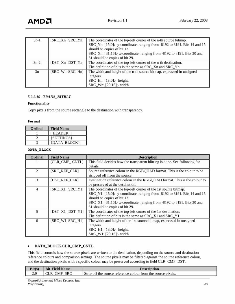
Revision 1.1 February 22, 2008
© 2008 Advanced Micro Devices, Inc. Proprietary 40
3n-1 [SRC_Xn | SRC_Yn] The coordinates of the top-left corner of the n-th source bitmap.
SRC_Yn: [15:0]:- y-coordinate, ranging from -8192 to 8191. Bits 14 and 15
should be copies of bit 13.
SRC_Xn: [31:16]:- x-coordinate, ranging from -8192 to 8191. Bits 30 and
31 should be copies of bit 29.
3n-2 [DST_Xn | DST_Yn] The coordinates of the top-left corner of the n-th destination.
The definition of bits is the same as SRC_Xn and SRC_Yn.
3n [SRC_Wn| SRC_Hn] The width and height of the n-th source bitmap, expressed in unsigned
integers.
SRC_Hn: [13:0]:- height.
SRC_Wn: [29:16]:- width.
5.2.2.10 TRANS_BITBLT
Functionality
Copy pixels from the source rectangle to the destination with transparency.
Format
Ordinal Field Name
1 [ HEADER ]
2 {SETTINGS}
3 {DATA_BLOCK}
DATA_BLOCK
Ordinal Field Name Description
1 [CLR_CMP_ CNTL] This field decides how the transparent blitting is done. See following for
details.
2 [SRC_REF_CLR] Source reference colour in the RGBQUAD format. This is the colour to be
stripped off from the source.
3 [DST_REF_CLR] Destination reference colour in the RGBQUAD format. This is the colour to
be preserved at the destination.
4 [SRC_X1 | SRC_Y1] The coordinates of the top-left corner of the 1st source bitmap.
SRC_Y1: [15:0]:- y-coordinate, ranging from -8192 to 8191. Bits 14 and 15
should be copies of bit 13.
SRC_X1: [31:16]:- x-coordinate, ranging from -8192 to 8191. Bits 30 and
31 should be copies of bit 29.
5 [DST_X1 | DST_Y1] The coordinates of the top-left corner of the 1st destination.
The definition of bits is the same as SRC_X1 and SRC_Y1.
6 [SRC_W1| SRC_H1] The width and height of the 1st source bitmap, expressed in unsigned
integers.
SRC_H1: [13:0]:- height.
SRC_W1: [29:16]:- width.
DATA_BLOCK.CLR_CMP_CNTL
This field controls how the source pixels are written to the destination, depending on the source and destination
reference colours and comparison settings. The source pixels may be filtered against the source reference colour,
and the destination pixels with a specific colour may be preserved according to field CLR_CMP_DST.
Bit(s) Bit-Field Name Description
2:0 CLR_CMP_SRC Strip off the source reference colour from the source pixels.

Revision 1.1 February 22, 2008
© 2008 Advanced Micro Devices, Inc. Proprietary 41
0 :- Do not strip off source pixels. All source pixels are written to the destination.
1 :- Block the blitting source. No source pixel is written to the destination.
2, 3 :- reserved.
4 :- The source pixels whose colour is equal to the reference colour are written to the
destination.
5 :- The source pixels whose colour is NOT equal to the reference colour are written
to the destination.
6 :- Reserved.
7 :- The source pixels whose colour is equal to the reference colour will be XORed
with the foreground colour of a mono bitmap, and then written to the destination.
That is, destPixel = srcPixel XOR foregrndColor if srcPixel is equal to the
foreground colour of a mono bitmap, specifically text. This is referred to as flipping
sometimes.
7:3 Reserved
10:8 CLR_CMP_DST Preserve pixels at the destination.
0 :- Do not preserve the destination pixels. All pixels from the source are written to
the destination.
1 :- Preserve all the destination pixels. No source pixel is written to the destination.
2, 3 :- Reserved.
4 :- The destination pixels whose colour is equal to the reference colour are
preserved. No source pixel is written on top of the pixels.
5 :- The destination pixels whose colour is NOT equal to the reference colour are
preserved.
6, 7 :- Reserved.
23:11 Reserved
25:24 CMP_ENABLE The bits controls what type of operation to be carried out.
0 :- Enable function CLR_CMP_DST.
1 :- Enable function CLR_CMP_SRC
2 :- Enable both CLR_CMP_SRC and CLR_CMP_DST. The final decision is based
on the agreement between decisions made separately.
3 :- Reserved.
31:26 Reserved
5.2.2.11 PLY_NEXTSCAN
Functionality
Draw a number of scanlines or polyscanlines using the current settings.
Format
Ordinal Field Name Description
1 [HEADER] The packet header
2 [HEIGHT | TOP ] TOP: [15:0] :- y-coordinate of the scanline/polyscanline.
HEIGHT: [31:16] :- The thickness of the line measured in pixels.
3 [END_1 | START_1] START_1: [15:0] :- the starting x-coordinate of the 1st dash.
END_1: [31:16]:- the ending x-coordinate of the 1st dash.
...
n+2 [END_n |START_n] START_n: [15:0] :- the starting x-coordinate of the 1st dash.
END_n: [31:16]:- the ending x-coordinate of the 1st dash.

Revision 1.1 February 22, 2008
© 2008 Advanced Micro Devices, Inc. Proprietary 42
5.2.2.12 LOAD_PALETTE
Functionality
Set up the 3D engine scaler and load a palette for a consequent 2D scaling operation.
Format
Ordinal Field Name Description
1 [HEADER] The packet header
2 [SCALE_DATATYPE ] 1:- The palette has 16 entries (4 bpp palette).
2:- The palette has 256 entries (8 bpp palette).
3 [ COLOR_1] The 1st
entry of the palette.
Data is in destination format (i.e. ARGB8888, RGB565, RGB555,…)
4 [ COLOR_2] The 2nd
entry of the palette. Bits are defined as above.
...
n+2 [ COLOR_n] The n-th entry of the palette. n = 16 (4bpp) or 256 (8bpp)
5.2.2.13 SET_SCISSORS
Functionality
Set the scissors to the given parameters.
Format
Ordinal Field Name Description
1 [HEADER] The packet header
2 [TOP_LEFT] [13:0] :- x-coordinate of the left edge of the clipping rectangle (in number of
pixels).
[29:16] :- y-coordinate of the top edge of the clipping rectangle (in number
of scanlines).
3 [ BOTTOM_RIGHT] [13:0] :- x-coordinate of the right edge of the clipping rectangle (in number
of pixels).
[29:16] :- y-coordinate of the bottom edge of the clipping rectangle (in
number of scanlines).
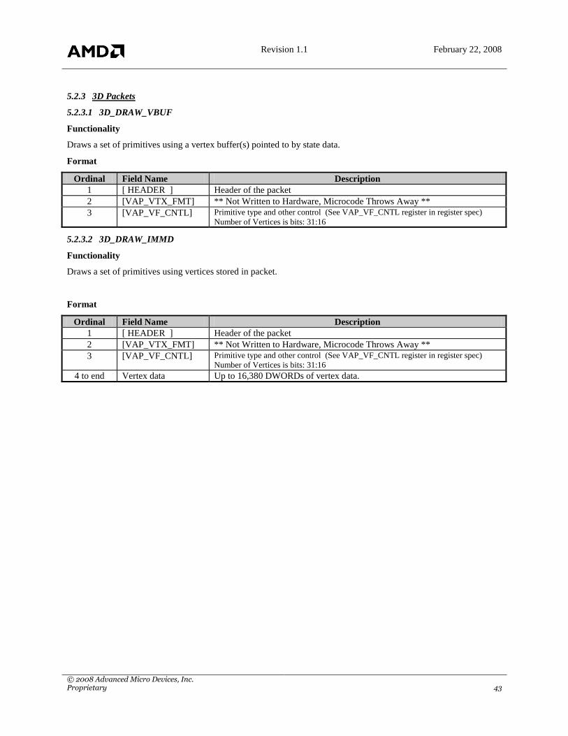
Revision 1.1 February 22, 2008
© 2008 Advanced Micro Devices, Inc. Proprietary 43
5.2.3 3D Packets
5.2.3.1 3D_DRAW_VBUF
Functionality
Draws a set of primitives using a vertex buffer(s) pointed to by state data.
Format
Ordinal Field Name Description
1 [ HEADER ] Header of the packet
2 [VAP_VTX_FMT] ** Not Written to Hardware, Microcode Throws Away **
3 [VAP_VF_CNTL] Primitive type and other control (See VAP_VF_CNTL register in register spec)
Number of Vertices is bits: 31:16
5.2.3.2 3D_DRAW_IMMD
Functionality
Draws a set of primitives using vertices stored in packet.
Format
Ordinal Field Name Description
1 [ HEADER ] Header of the packet
2 [VAP_VTX_FMT] ** Not Written to Hardware, Microcode Throws Away **
3 [VAP_VF_CNTL] Primitive type and other control (See VAP_VF_CNTL register in register spec)
Number of Vertices is bits: 31:16
4 to end Vertex data Up to 16,380 DWORDs of vertex data.

Revision 1.1 February 22, 2008
© 2008 Advanced Micro Devices, Inc. Proprietary 44
5.2.3.3 3D_DRAW_INDX
Functionality
Draws a set of primitives using a vertex buffer(s) pointed to by state data, index from indices in packet. Indices are
either 16-bit or 32-bit.
Format
Ordinal Field Name Description
1 [ HEADER ] Header of the packet
2 [VAP_VTX_FMT] ** Not Written to Hardware, Microcode Throws Away **
3 [VAP_VF_CNTL] Primitive type and other control (See VAP_VF_CNTL register in register spec)
Number of Vertices is bits: 31:16
4 to end [indx16 #2 | indx16 #1]
or [indx32] Up to or 32,760 16-bit indices or 16,380 32-bit indices to vertex data pointed
to by state registers. The INDEX_SIZE field in the VAP_VF_CNTL register
indicates whether the indices are 16-bit or 32-bit. See INDX_BUFFER
packet for support of more indices.
5.2.3.4 3D_DRAW_VBUF_2
Functionality
Draws a set of primitives using a vertex buffer(s) pointed to by state data.
Format
Ordinal Field Name Description
1 [ HEADER ] Header of the packet
2 [VAP_VF_CNTL] Primitive type and other control (See VAP_VF_CNTL register in register spec)
Number of Vertices is bits: 31:16

Revision 1.1 February 22, 2008
© 2008 Advanced Micro Devices, Inc. Proprietary 45
5.2.3.5 3D_DRAW_IMMD_2
Functionality
Draws a set of primitives using vertices stored in packet.
Format
Ordinal Field Name Description
1 [ HEADER ] Header of the packet
2 [VAP_VF_CNTL] Primitive type and other control (See VAP_VF_CNTL register in register spec)
Number of Vertices is bits: 31:16
3 to end Vertex data Up to 16,381 DWORDs of vertex data
5.2.3.6 3D_DRAW_INDX_2
Functionality
Draws a set of primitives using a vertex buffer(s) pointed to by state data, index from indices in packet.
Format
Ordinal Field Name Description
1 [ HEADER ] Header of the packet
2 [VAP_VF_CNTL] Primitive type and other control (See VAP_VF_CNTL register in register spec)
Number of Vertices is bits: 31:16
3 to end [indx16 #2 | indx16 #1]
or [indx32 #1] Up to or 32762 16-bit indices or 16,381 32-bit indices to vertex data pointed
to by state registers. The INDEX_SIZE field in the VAP_VF_CNTL register
indicates whether the indices are 16-bit or 32-bit. See INDX_BUFFER
packet for support of more indices.
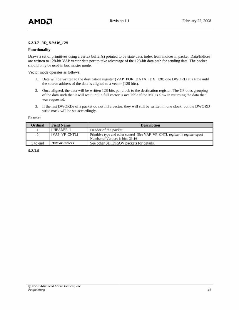
Revision 1.1 February 22, 2008
© 2008 Advanced Micro Devices, Inc. Proprietary 46
5.2.3.7 3D_DRAW_128
Functionality
Draws a set of primitives using a vertex buffer(s) pointed to by state data, index from indices in packet. Data/Indices
are written to 128-bit VAP vector data port to take advantage of the 128-bit data path for sending data. The packet
should only be used in bus master mode.
Vector mode operates as follows:
1. Data will be written to the destination register (VAP_POR_DATA_IDX_128) one DWORD at a time until
the source address of the data is aligned to a vector (128 bits).
2. Once aligned, the data will be written 128-bits per clock to the destination register. The CP does grouping
of the data such that it will wait until a full vector is available if the MC is slow in returning the data that
was requested.
3. If the last DWORDs of a packet do not fill a vector, they will still be written in one clock, but the DWORD
write mask will be set accordingly.
Format
Ordinal Field Name Description
1 [ HEADER ] Header of the packet
2 [VAP_VF_CNTL] Primitive type and other control (See VAP_VF_CNTL register in register spec)
Number of Vertices is bits: 31:16
3 to end Data or Indices See other 3D_DRAW packets for details.
5.2.3.8

Revision 1.1 February 22, 2008
© 2008 Advanced Micro Devices, Inc. Proprietary 47
5.2.3.9 3D_LOAD_VBPNTR
Functionality
Load the vertex arrays pointers.
Format
Ordinal Field Name Description
1 [ HEADER ] Header of the packet
2 VTX_NUM_ARRAYS Number of arrays
3 VTX_AOS_ATTR01 Control for the first two arrays
4 VTX_AOS_ADDR0 Pointer to first array
5 VTX_AOS_ADDR1 Pointer to second array
6 VTX_AOS_ATTR23 And so on….
7 VTX_AOS_ADDR2
8 VTX_AOS_ADDR3
9 VTX_AOS_ATTR45
10 VTX_AOS_ADDR4
11 VTX_AOS_ADDR5
12 VTX_AOS_ATTR67
13 VTX_AOS_ADDR6
14 VTX_AOS_ADDR7
15 VTX_AOS_ATTR89
16 VTX_AOS_ADDR8
17 VTX_AOS_ADDR9
18 VTX_AOS_ATTR1011
19 VTX_AOS_ADDR10
20 VTX_AOS_ADDR11
5.2.3.10 3D_CLEAR_HIZ
Functionality
Clear HIZ RAM.
Format
Ordinal Field Name Description
1 [ HEADER ] Header of the packet
2 START Start
3 COUNT[13:0] Count[13:0] – Maximum is 0x3FFF.
4 CLEAR_VALUE The value to write into the HIZ RAM.
5.2.3.11 INDX_BUFFER
Functionality
Initiates Indirect Buffer #2 (IB #2) to fetch data that is written to the destination address. The main reason for this
packet is to fetch indices from an index buffer. The packet however can be used to fetch any type of data and write it
to destination address(s) in the chip.
To process an index buffer, first issue a 3D_DRAW_INDX packet with only the VAP_VTX_FMT and
VAP_VF_CNTL DWORDs (i.e. count = 1). Then process an INDX_BUFFER packet to supply the indices that
would have otherwise been in the 3D_DRAW_INDX packet. Note: For a 3D_DRAW_INDX_2 packet, the
VAP_VTX_FMT is not present and the count in the header should be zero.
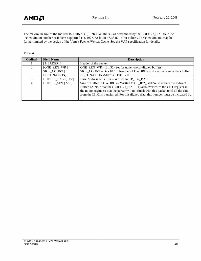
Revision 1.1 February 22, 2008
© 2008 Advanced Micro Devices, Inc. Proprietary 48
The maximum size of the Indirect #2 Buffer is 8,192K DWORDs – as determined by the BUFFER_SIZE field. So
the maximum number of indices supported is 8,192K 32-bit or 16,384K 16-bit indices. These maximums may be
further limited by the design of the Vertex Fetcher/Vertex Cache. See the VAP specification for details.
Format
Ordinal Field Name Description
1 [ HEADER ] Header of the packet
2 [ONE_REG_WR |
SKIP_COUNT |
DESTINATION]
ONE_REG_WR – Bit 31 (Set for upper-word-aligned buffers)
SKIP_COUNT – Bits 18:16: Number of DWORDs to discard at start of data buffer
DESTINATION Address – Bits 12:0
3 BUFFER_BASE[31:2] Base Address of Buffer – Written to CP_IB2_BASE
4 BUFFER_SIZE[22:0] Size of Buffer in DWORDs – Written to CP_IB2_BUFSZ to initiate the Indirect
Buffer #2. Note that the (BUFFER_SIZE – 1) also overwrites the CNT register in
the micro engine so that the parser will not finish with this packet until all the data
from the IB #2 is transferred. For misaligned data, this number must be increased by
1.

Revision 1.1 February 22, 2008
© 2008 Advanced Micro Devices, Inc. Proprietary 49
5.2.3.12 MPEG_INDEX
Functionality
Packed register writes for MPEG and Generation of Indices.
Format
Ordinal Field Name Description
1 [ HEADER ] Header field of the packet.
2 [MASK] DWORD write Mask: Bits 15:0 are “present” bits to indicate whether to
write the register:
bit[0] VAP_PVS_CODE_CNTL_0 present
bit[1] VAP_PVS_CODE_CNTL_1 present
bit[2] VAP_PROG_STREAM_CNTL_0 present
bit[3] VAP_PROG_STREAM_CNTL_1 present
bit[4] VAP_PROG_STREAM_CNTL_2 present
bit[5] VAP_PROG_STREAM_CNTL_3 present
bit[6] VAP_OUT_VTX_FMT_0 present
bit[7] VAP_OUT_VTX_FMT_1 present
bit[8] VAP_VTX_NUM_ARRAYS present
bit[9] RS_COUNT present
bit[10] RS_INST_COUNT present
bit[11] TX_ENABLE present
bit[12] US_CODE_ADDR_0 present
bit[13] US_CODE_ADDR_1 present
bit[14] US_CODE_ADDR_2 present
bit[15] US_CODE_ADDR_3 present
bit[16] US_CONFIG present
bit[17] RB3D_DSTCACHE_CTLSTAT present
bit[18] RB3D_COLOROFFSET0 present
bit[19] RB3D_COLORPITCH0 present
Conditional [Register Values] Values to Write into Registers. Only present in packet if corresponding

Revision 1.1 February 22, 2008
© 2008 Advanced Micro Devices, Inc. Proprietary 50
3 up to 22 “present” bit is set in the MASK.
Next [VF_CNTL] Written Unconditional to VAP_VF_CNTL register
Next+1 [NUM_INDICES] Number of Index Base Values (0x3FFF Maximum)
Next+2 to
Next+2+
NUM_INDIC
ES
[FIRST_INDEX] First Index of Quad. (0x0000 to 0xFFFC)
For each “First Index”, CP will generate the other 3 indices and output:
FIRST_INDEX
FIRST_INDEX+1
FIRST_INDEX+2
FIRST_INDEX+3
Last Values [DUMMY] Any value is fine. Any number of dummy values are supported.

Revision 1.1 February 22, 2008
© 2008 Advanced Micro Devices, Inc. Proprietary 51
5.2.4 PRED_EXEC
Functionality
Perform a predicated execution of a sequence of packets (type 0, 2, and type 3) on select devices.
Format
Ordinal Field Name Description
1 [ HEADER ] Header field of the packet.
2 [DEVICE_SELECT |
EXEC_COUNT]
DEVICE_SELECT: [31:24] – bitfield to select one or more device upon
which the subsequent predicated packets will be executed
EXEC_COUNT: [22:0] – total number of DWORDs of subsequent
predicated packets. This count wraps the packets that will be predicated
by the device select.
5.2.4.1 WAIT_SEMAPHORE
Functionality
Wait for a semaphore to be zero before continuing to process the subsequent command stream. There are four
microcode ram slots set aside for use as semaphores. These are at offset 0xFC-0xFF.
Notes
The driver/application executing on the CPU can write non-zero values at any time to semaphore memory. The
application can write a non-zero value to cause the CP micro-engine to pause at the next WAIT_SEMAPHORE
packet in the command stream. This has the affect of pausing all GPU rendering that is queued in the indirect and
ring buffers. The application can then write a zero to the semaphore to allow the micro-engine to proceed.
The application can write to the semaphore memory by a direct (PIO) register write to two registers:
1. Write the semaphore offset (0xFC, 0xFD, 0xFE, or 0xFF) to the CP_ME_RAM_ADDR register.
2. Write the semaphore value (zero or non-zero) to the CP_ME_RAM_DATAL register.
Format
Ordinal Field Name Description
1 [ HEADER ] Header field of the packet.
2 Semaphore offset This is the desired semaphore to test in the wait loop. This can be any one of
0xFC, 0xFD, 0xFE, 0xFF.
3 Semaphore reset Optional. This value, if present, is written to the semaphore offset once the
wait loop has been satisfied (i.e., once the semaphore is zero).

Revision 1.1 February 22, 2008
© 2008 Advanced Micro Devices, Inc. Proprietary 52
5.2.5 Miscellaneous Packets
5.2.5.1 COND_EXEC
Functionality
Perform a conditional execution of a sequence of packets (type 0, 2, and type 3) based on a boolean stored in GPU-
accessible video memory.
This packet use the Indirect Buffer #2 (IB2) to read the boolean in memory. Therefore, this packet can not be
initiated from an IB2.
Notes
Care must be taken to make certain that EXEC_COUNT contains the exact number of DWORDs for the subsequent
packets that are to be conditionally executed. The microengine will start parsing the DWORD immediately
following EXEC_COUNT DWORDs. If this is not a packet header, the device will encounter corruption or hang.
Format
Ordinal Field Name Description
1 [ HEADER ] Header field of the packet.
2 TWO This value must be 2
3 EXEC_COUNT EXEC_COUNT: [22:0] – total number of DWORDs of subsequent
conditional packets. This count wraps the packets that will be
conditionally executed.
5.2.5.2 WAIT_MEM
Functionality
Wait for a GPU-accessible memory semaphore to be zero before continuing to process the subsequent command
stream. The semaphore can reside in any GPU-accessible memory (local or non-local). The base address of the
semaphore must be aligned to a DWORD boundary. The semaphore in memory consists of two DWORDs.
This packet has no ability to increment, decrement or otherwise change the contents of the memory semaphore.
The memory semaphore consists of two DWORDs: the actual semaphore and an extra DWORD with a fixed value
of two. The extra DWORD is required and guarantees that the command processor micro-engine can loop properly
in order to repeatedly test the semaphore value as necessary. The semaphore is organized as follows:
Semaphore value
Fixed value of 2
This packet use the Indirect Buffer #2 (IB2) to read the memory semaphore. Therefore, this packet can not be
initiated from an IB2.
Notes
If both ordinal 3 (SEM_LEN) and the DWORD in memory following the semaphore value is not equal to two, the
CP micro-engine will become confused and ultimately hang the hardware.
The driver/application executing on the CPU can write non-zero values at any time to semaphore memory. The
application can write a non-zero value to cause the CP micro-engine to pause at the next WAIT_MEM packet in the

Revision 1.1 February 22, 2008
© 2008 Advanced Micro Devices, Inc. Proprietary 53
command stream. This has the affect of pausing all GPU rendering that is queued in the indirect and ring buffers.
The application can then write a zero to the semaphore to allow the micro-engine to proceed.
Format
Ordinal Field Name Description
1 [ HEADER ] Header field of the packet.
2 SEM_ADDR[31:2] Memory semaphore device address (DWORD aligned)
This value is written to the CP_IB2_BASE in order to read the semaphore
3 SEM_LEN Memory semaphore length
This value MUST be 2
This value is written to the CP_IB2_BUFSIZ in order to read the semaphore
the first time
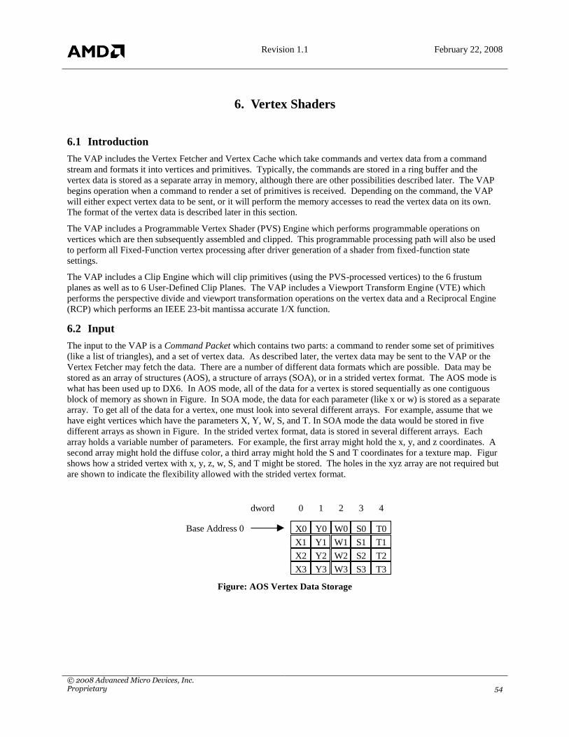
Revision 1.1 February 22, 2008
© 2008 Advanced Micro Devices, Inc. Proprietary 54
6. Vertex Shaders
6.1 Introduction
The VAP includes the Vertex Fetcher and Vertex Cache which take commands and vertex data from a command
stream and formats it into vertices and primitives. Typically, the commands are stored in a ring buffer and the
vertex data is stored as a separate array in memory, although there are other possibilities described later. The VAP
begins operation when a command to render a set of primitives is received. Depending on the command, the VAP
will either expect vertex data to be sent, or it will perform the memory accesses to read the vertex data on its own.
The format of the vertex data is described later in this section.
The VAP includes a Programmable Vertex Shader (PVS) Engine which performs programmable operations on
vertices which are then subsequently assembled and clipped. This programmable processing path will also be used
to perform all Fixed-Function vertex processing after driver generation of a shader from fixed-function state
settings.
The VAP includes a Clip Engine which will clip primitives (using the PVS-processed vertices) to the 6 frustum
planes as well as to 6 User-Defined Clip Planes. The VAP includes a Viewport Transform Engine (VTE) which
performs the perspective divide and viewport transformation operations on the vertex data and a Reciprocal Engine
(RCP) which performs an IEEE 23-bit mantissa accurate 1/X function.
6.2 Input
The input to the VAP is a Command Packet which contains two parts: a command to render some set of primitives
(like a list of triangles), and a set of vertex data. As described later, the vertex data may be sent to the VAP or the
Vertex Fetcher may fetch the data. There are a number of different data formats which are possible. Data may be
stored as an array of structures (AOS), a structure of arrays (SOA), or in a strided vertex format. The AOS mode is
what has been used up to DX6. In AOS mode, all of the data for a vertex is stored sequentially as one contiguous
block of memory as shown in Figure. In SOA mode, the data for each parameter (like x or w) is stored as a separate
array. To get all of the data for a vertex, one must look into several different arrays. For example, assume that we
have eight vertices which have the parameters X, Y, W, S, and T. In SOA mode the data would be stored in five
different arrays as shown in Figure. In the strided vertex format, data is stored in several different arrays. Each
array holds a variable number of parameters. For example, the first array might hold the x, y, and z coordinates. A
second array might hold the diffuse color, a third array might hold the S and T coordinates for a texture map. Figur
shows how a strided vertex with x, y, z, w, S, and T might be stored. The holes in the xyz array are not required but
are shown to indicate the flexibility allowed with the strided vertex format.
X0 Y0 W0 S0
T2
X1 Y1 W1 S1
T3
X2 Y2 W2 S2
X3 Y3 W3 S3
T1
T0Base Address 0
dword 0 1 2 3 4
Figure: AOS Vertex Data Storage

Revision 1.1 February 22, 2008
© 2008 Advanced Micro Devices, Inc. Proprietary 55
X0 X1 X2 X3
Y0 Y1 Y2 Y3
W0 W1 W2 W3
S0 S1 S2 S3
T0 T1 T2 T3
Base Address 0
Base Address 1
Base Address 2
Base Address 3
Base Address 4
dword 0 1 2 3
Figure: SOA Vertex Data Storage
X0 Y0 Z0 X1 Y1 Z1
W0 W1 W2 W3
S0 T0 S1 T1 S2 T2 S3 T3
Base Address 0
Base Address 1
Base Address 2
dword 0 1 2 3 4 5 6 7
X2 Y2 Z2
8 9 10 11
X3 Y3 Z3
12 13 14 15
Figure: Strided Vertex Data Storage
To represent all of these formats, the Vertex Fetcher architecture allows for a vertex to be described as multiple
arrays of structures. Each array is described with a base address, a count and a stride. The base address points to
the beginning of the array. The count indicates the number of dwords of vertex data in this array. The stride gives
the number of dwords to the next structure in the array of structures. The AOS vertex from Figure with 5 parameters
would be represented with a single array which consists of 5 dwords with a stride of 5 dwords. The SOA vertex
from Figure would be represented with 5 arrays. Each array would have a count of 1 and a stride of 1. The strided
vertex from Figur would be represented with three arrays. The first array would have a count of 3 and a stride of 4.
The second array would have a count of 1 and a stride of 1. The third array would have a count of 2 and a stride of
2. A given implementation of this architecture may have a different maximum number of arrays of structures. If
only AOS is supported, then only one array is required. To support a strided vertex format with three textures, 7
arrays would be required (xyz, w, diffuse, specular, S0T0, S1T1, S2T2.) To support a true SOA mode, each
parameter would require its own array.
The access to vertex data may be immediate or by an index. In immediate mode, the base address of an array of
vertex data is provided. The vertex data should be read in the order in which it is stored to produce the desired
primitives. In indexed mode, a base address to the beginning of the vertex data is provided along with a set of
indices. The indices are used to access vertices in any order.
The vertex indices are clamped between a minimum and maximum state value which is supplied by the driver. This
prevents making requests to illegal or unavailable memory addresses.
Finally, the vertex data can be embedded as part of the command stream, or it can be stored in a separate array. The
figure below shows all of the possible vertex data storage modes along with implementation details for each mode.

Revision 1.1 February 22, 2008
© 2008 Advanced Micro Devices, Inc. Proprietary 56
The table below describes the parameters that may be in a vertex, as supplied to the graphics controller
device.
NOTE: With the R300 PVS-only vertex processing path and PSC-only input vertex data mapping path, the
TCL (or PVS) input memories have no pre-defined mapping to vertex values. This is completely determined
by the driver FF->PVS conversion process. Due to this fact, the table below is fairly meaningless to the vertex
process. It is retained as a guide to help describe the fixed-function possibilities for vertex data.
Type Param
eter
Description Format Applicable
Interface
(PRE-TNL /
POST-TNL
/ BOTH)**
Position0 XY X0 The x coordinate of the vertex IEEE floating point BOTH
Y0 The y coordinate of the vertex IEEE floating point BOTH
Position0 Z Z0 The z coordinate of the vertex IEEE floating point BOTH
Position0 W W0 W or RHW (1/Homog W) coordinate of the
vertex
IEEE floating point BOTH
Vertex Blending
Weight(s)
BW0-4 0-4 Blend Weights IEEE floating point PRE-TNL
Per-Vertex Matrix
Select
PVMS Vertex Blending Matrix Selects 8888 packed fixed point PRE-TNL
Vertex Normal 0 Nx0 The x coordinate of the vertex normal IEEE floating point PRE-TNL
Ny0 The y coordinate of the vertex normal IEEE floating point PRE-TNL
Nz0 The z coordinate of the vertex normal IEEE floating point PRE-TNL
Point Size Modifier PS Point Size Modifier – Point Sprites – Post-
TCL only
IEEE floating point BOTH
Discrete Fog F Fog value – Post TCL only IEEE floating point POST-TNL
Shininess0 Shine0 Used for GL Material Per-Vertex Support IEEE floating point PRE-TNL
Shininess1 Shine1 Used for GL Material Per-Vertex Support IEEE floating point PRE-TNL
Color 0 ARGB Typically Diffuse color and alpha weight Usually 8888, but can be
three or four separate IEEE
floating point values **
BOTH

Revision 1.1 February 22, 2008
© 2008 Advanced Micro Devices, Inc. Proprietary 57
Color 1 ARGB Typically Specular color and fog/alpha weight Usually 8888, but can be
three or four separate IEEE
floating point values **
BOTH
Color 2 ARGB Typically Used for GL Material Per-Vertex
Support
Usually 8888, but can be
three or four separate IEEE
floating point values **
PRE-TNL
Color 3 ARGB Typically Used for GL Material Per-Vertex
Support
Usually 8888, but can be
three or four separate IEEE
floating point values **
PRE-TNL
Color 4 ARGB Typically Used for GL Material Per-Vertex
Support
Usually 8888, but can be
three or four separate IEEE
floating point values **
PRE-TNL
Color 5 ARGB Typically Used for GL Material Per-Vertex
Support
Usually 8888, but can be
three or four separate IEEE
floating point values **
PRE-TNL
Color 6 ARGB Typically Used for GL Material Per-Vertex
Support
Usually 8888, but can be
three or four separate IEEE
floating point values **
PRE-TNL
Color 7 ARGB Typically Used for GL Material Per-Vertex
Support
Usually 8888, but can be
three or four separate IEEE
floating point values **
PRE-TNL
Texture Coordinate
Set 0
S0 The 1st coordinate for texture number 0
(usually the single dimension horizontal
component S )
IEEE floating point BOTH
T0 The 2nd coordinate for texture number 0
(usually the two dimension vertical
component T )
IEEE floating point BOTH
R0 The 3rd coordinate for texture number 0
(The 3rd
& 4th components can have many
uses)*
IEEE floating point BOTH
Q0 The 4th coordinate for texture number 0
(The 3rd
& 4th components can have many
uses)*
IEEE floating point BOTH
Texture Coordinate S1 The 1st coordinate for texture number 1 IEEE floating point BOTH
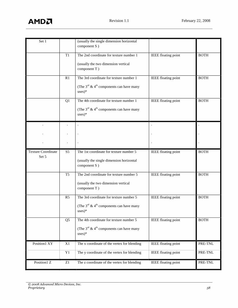
Revision 1.1 February 22, 2008
© 2008 Advanced Micro Devices, Inc. Proprietary 58
Set 1 (usually the single dimension horizontal
component S )
T1 The 2nd coordinate for texture number 1
(usually the two dimension vertical
component T )
IEEE floating point BOTH
R1 The 3rd coordinate for texture number 1
(The 3rd
& 4th components can have many
uses)*
IEEE floating point BOTH
Q1 The 4th coordinate for texture number 1
(The 3rd
& 4th components can have many
uses)*
IEEE floating point BOTH
.
.
.
.
.
.
.
.
.
.
.
.
.
.
.
Texture Coordinate
Set 5
S5 The 1st coordinate for texture number 5
(usually the single dimension horizontal
component S )
IEEE floating point BOTH
T5 The 2nd coordinate for texture number 5
(usually the two dimension vertical
component T )
IEEE floating point BOTH
R5 The 3rd coordinate for texture number 5
(The 3rd
& 4th components can have many
uses)*
IEEE floating point BOTH
Q5 The 4th coordinate for texture number 5
(The 3rd
& 4th components can have many
uses)*
IEEE floating point BOTH
Position1 XY X1 The x coordinate of the vertex for blending IEEE floating point PRE-TNL
Y1 The y coordinate of the vertex for blending IEEE floating point PRE-TNL
Position1 Z Z1 The z coordinate of the vertex for blending IEEE floating point PRE-TNL
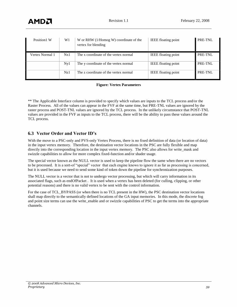
Revision 1.1 February 22, 2008
© 2008 Advanced Micro Devices, Inc. Proprietary 59
Position1 W W1 W or RHW (1/Homog W) coordinate of the
vertex for blending
IEEE floating point PRE-TNL
Vertex Normal 1 Nx1 The x coordinate of the vertex normal IEEE floating point PRE-TNL
Ny1 The y coordinate of the vertex normal IEEE floating point PRE-TNL
Nz1 The z coordinate of the vertex normal IEEE floating point PRE-TNL
Figure: Vertex Parameters
** The Applicable Interface column is provided to specify which values are inputs to the TCL process and/or the
Raster Process. All of the values can appear in the FVF at the same time, but PRE-TNL values are ignored by the
raster process and POST-TNL values are ignored by the TCL process. In the unlikely circumstance that POST-TNL
values are provided in the FVF as inputs to the TCL process, there will be the ability to pass these values around the
TCL process.
6.3 Vector Order and Vector ID‟s
With the move to a PSC-only and PVS-only Vertex Process, there is no fixed definition of data (or location of data)
in the input vertex memory. Therefore, the destination vector locations in the PSC are fully flexible and map
directly into the corresponding location in the input vertex memory. The PSC also allows for write_mask and
swizzle capabilities to allow for more complex fixed-function and/or shader usage.
The special vector known as the NULL vector is used to keep the pipeline flow the same when there are no vectors
to be processed. It is a sort-of “special” vector that each engine knows to ignore it as far as processing is concerned,
but it is used because we need to send some kind of token down the pipeline for synchronization purposes.
The NULL vector is a vector that is not to undergo vector processing, but which will carry information in its
associated flags, such as endOfPacket . It is used when a vertex has been deleted (for culling, clipping, or other
potential reasons) and there is no valid vertex to be sent with the control information.
For the case of TCL_BYPASS (or when there is no TCL present in the HW), the PSC destination vector locations
shall map directly to the semantically defined locations of the GA input memories. In this mode, the discrete fog
and point size terms can use the write_enable and or swizzle capabilities of PSC to get the terms into the appropriate
channels.

Revision 1.1 February 22, 2008
© 2008 Advanced Micro Devices, Inc. Proprietary 60
6.4 VAP Registers
6.4.1 VAP Vertex Data Port Registers
The DATA and IDX PORT registers are written with either primitive vertex data or primitive vertex indices after a
“trigger” write has occurred. A “trigger” write is a write to the VAP_VF_CNTL register with a non-zero prim_type.
The correct (expected) number of data words or index words must be written to these registers or undefined
behavior will result.
For R300, there is a new DATA/IDX port register added for 128-bit access. This register is only accessible via a
PM4 Type3 packet and can only be used for indexed TRI_LIST and LINE_LIST. Other than the prim-type
limitations, using this 128-bit register (or PM4 Type 3 packet opcode) is identical to using the standard method.
The PRIM_WALK field in the VAP_VF_CNTL register defines what method of vertex data or indx updates are to
occur.
1 = Indexes (Indices embedded in command stream; vertex data to be fetched from memory)
In this mode, vertex indices are written to the DATA/IDX port registers. Data is fetched using the AOS registers
corresponding to the indices in the input list. The number of indices expected is
VAP_VF_CNTL.NUM_VERTICES – 1. This mode does not use the VAP_VTX_SIZE register. The size of the
vertices is determined by the AOS register setup.
2 = Vertex List (Vertex data to be fetched from memory)
This mode does not require any vertex data or vertex indices written to the DATA/IDX port registers. Data is
fetched using the AOS registers for the indices from 0 to VAP_VF_CNTL.NUM_VERTICES – 1. Identical to
Indexes mode, except indices are internally generated.
3 = Vertex Data (Vertex data embedded in command stream)
In this mode, the vertex data is written to the DATA port registers. The number of DWORDS expected is
VAP_VTX_SIZE.DWORDS_PER_VTX * (VAP_VF_CNTL.NUM_VERTICES – 1). The VAP_VTX_SIZE
register is new to R300. In R100 / R200, this size was derived from the VAP_VTX_FMT_0/1.
6.4.2 VAP Control Register
The PVS_NUM_SLOTS should be set to the minimum of
the MAX_SLOTS, (POR is 10)
the INPUT_VTX_MEM_SIZE / INPUT_VECTORS_PER_VTX (POR is 128 / Var)
the OUPUT_VTX_MEM_SIZE / OUTPUT_VECTORS_PER_VTX (POR is 128 / Var)
These equations assume the input and output vertex data has been packed. If not, use the
MAX_INPUT_VECTOR_USED instead of INPUT_VECTORS_PER_VTX
The PVS_NUM_CNTLRS should be set to the minimum of
the MAX_CNTLRS, (POR is 6)
the TEMP_VTX_MEM_SIZE / TEMP_VECTORS_PER_VTX (POR is 128 / Var)
Revision 1.1 February 22, 2008
© 2008 Advanced Micro Devices, Inc. Proprietary 61
These equations assume the temp vertex data has been packed. If not, use the MAX_TEMP_VECTOR_USED
instead of TEMP_VECTORS_PER_VTX.
When modifying either of PVS_NUM_SLOTS or PVS_NUM_CNTLRS, a flush must be inserted prior to the
update.
The PVS_NUM_FPUS will typically remain constant for a given chip, but can be used for performance testing.
The Shader HW will support up to a max of 32 vectors-per-vertex of input data and 32-vectors-per-vertex of temp
data as long as the NUM_SLOTS and NUM_CNTLRS are set to obey the above-described rules.
New R5xx Fields
The TCL_STATE_OPTIMIZATION bit enables a hardware optimization to improve small batch and
multiple instance performance. The TCL_STATE_OPTIMIZATION is a bit which should be set all the time.
The bit can be reset to return operation to pre-R5xx status.
6.4.3 R300 Edge Flag Support Description
Edge Flags refers to the bits which are provided, generated and/or modified during the primitive process which
affect which edges (lines) or points of a triangle are drawn when in a wireframe or point fill mode. Edge Flags are
not applicable to line or point primitive types, but are applicable to all 3 or more-sided primitives (i.e quad, polygon,
etc). R300 will support edge flags for wireframe rendering as follows :
1. Prim Type initialization of edge flags is done by the vertex fetcher logic. Edge flags are initialized
by the vertex fetcher based on the VAP_VF_CNTL.PRIM_TYPE field. The edge flags values for
points and lines are not used during the triangle fill process, so are irrelevant. The edge flags for all
triangle primitive types are all 3 set. For more complex prim types like quads and polygons, only
the exterior of the primitive is supposed to be drawn, so the vertex fetcher applies the edge flags in a
way which only sets the bits which correspond to an external edge of the supplied primitive.
2. Clipping modification of edge flags is done by the clipping processor according to the OpenGL
specification. Basically, the rule is that edges introduced by clipping (which would lie along a clip
plane) will always have thier corresponding edge flag set and edges which are fragments of initial
edges would retain thier original edge flags. The boundary edges introduced by clipping may be
either always set or never based on the VAP_CLIP_CNTL.BOUNDARY_EDGE_FLAG_ENA bit.
6.4.4 Input Vertex Format Registers
The VAP_VTX_FMT_0 and VAP_VTX_FMT_1 registers were used for 2 reasons on R200:
1. Decoding / Data Conversion / Data Direction of Vertex Stream Data from output of Cache to Vector
ID‟s
2. Computation of Dwords/Vtx for Command Stream load of vertex data.
These registers will no longer exist for R300. They are replaced as follows:
The Decoding / Data Conversion / Data Direction will be controlled completely by the Programmable
Stream Control logic. R300 will contain the additional functionality of component swizzle and write-
mask specification to ensure full control of input stream.
The computation of Dwords/Vtx will be replaced by the VAP_VTX_SIZE register which must be
loaded by the driver when using command stream vertex data.
6.4.5 TCL Output Vertex Format Registers
The purpose of these controls is to indicate which vertex data should be transmitted from the PVS output vertex

Revision 1.1 February 22, 2008
© 2008 Advanced Micro Devices, Inc. Proprietary 62
memories, and from which vector locations they come. The PVS output vertex memories are not directly mapped to
semantic values to enable the split-vertex mode described later. The RASTER_VTX_FMT_0/1registers define
which values will be transmitted from PVS to CLIP/Setup to GA to Raster.
The locations of the vectors in the PVS output memory must be packed based on the VAP_OUT_VTX_FMT_0/1
register settings. Only the fields which are present in the OVFRs should be packed in the output memory. The
packing order is as follows: Position is always in location 0, Point Size (if present) is next (Point Size consumes an
entire vector in the memory, the X-channel is the value used by the raster), Colors (0-3) are next (if present), and
Textures (0-7) are next (if present). For example if the OVFR specified POS, PNT_SIZE, C0, C2, T1 and T5, these
vectors should be mapped (by the shader output operand offsets) to Output Memory locations 0-5 respectively.
For Points (Sprites) using Tex Gen (GB_ENABLE.TEX#_SOURCE == STUFF), the
VAP_OUT_VTX_FMT_1.TEX# should not be set. This is because, in general, there is no texture coordinate data
transferred from VAP to GA for this case. In the case of point clipping with tex gen, VAP will send these texture
coordinates to the GA even though the OVFR bit is not set, as follows:
OVFR COUNT STUFF TEX DESIRED CHANGED RESULT
0 0 No texture ever
0 >0 Clipper and/or GA creates (stuffs)
texture
>0 0 Normal texture (use vertex/pvs
texture)
>0 >0 Normal texture (use vertex/pvs
texture)
There is also the ability to pack 2 2-dimensional textures into a single 4-component texture for the VAP->GA
interface by only specifying one texture and mapping the raster state to think it is two textures.
6.4.6 Vertex State Control
This vector controls how the per-vertex state is processed. This input method is designed for OpenGL Immediate
Mode and Display List Processing.
UPDATE_USER_COLOR_0/1_ENA are deleted from R300 since they are not needed, only one user color is
required.
The COLOR_#_ASSEMBLY_CNTL change from 2-bit fields on R200 to 1-bit fields on R300 since there is only 1
USER COLOR.
6.4.7 Programmable Input Stream Control Registers
These registers control the post-vertex-cache mapping of input vertex stream data to the vector ids for TCL or SE
input memories. These registers replace the R200 Input Vertex Format Registers. Terminology: A vertex is
composed of multiple (up to 16 for R300) streams. A stream can be composed of multiple elements (where an
element is pos or norm or texcoord). The control data is arranged as 16 sets of element control data. There is not
necessarily a one-for-one mapping of stream to element. The stream control shall be set up in the order that the data
is received (or fetched).
The DataType specifies the number of DWORDS and format for each input element.
The SkipDwords specifies the number of DWORDS to skip (discard from the input stream) after the corresponding

Revision 1.1 February 22, 2008
© 2008 Advanced Micro Devices, Inc. Proprietary 63
element has been processed. This allows multiple non-contiguous elements to reside within one stream. NOTE:
There is not support for skipping DWORDS prior to the first element, the assumption is that the driver can
prevent this from occurring.
There are two sets of PSC control registers, the VAP_PROG_STREAM_CNTL_0-7 are identical to the R200
registers of the same name. R300 adds VAP_PROG_STREAM_CNTL_EXT_0-7 which are extensions to the first
set of registers to allow a swizzle and write_mask capability. The expectation is that the EXT registers will not be
updated frequently, but they must be updated at least once to provide default control.
The DstVecLoc specifies the destination vector location (TCL / SE input vector address) for the given element.
The data type of FLOAT_8 has been added to R300 to permit using input vertices greater than 16 vectors. By
making sure that the VAP_CNTL.PVS_NUM_SLOTS and VAP_CNTL.PVS_NUM_CNTLRS are appropriately
sized, it is possible to use up to 32 vectors for the input vertex representation.
6.4.8 PVS State Flush Register
Since the driver is given control over multi-state updates to PVS Code and Constant memories, there is the need for
the driver to be able to force a “flush” of the state data. When this register address is written, the State Block will
force a flush of TCL processing so that both versions of TCL state are available before updates are processed. This
register is write only, and the data that is written is unused.
6.4.9 PVS Vertex Timeout Register
A condition can occur in the HW, in pathological vertex reuse cases, where when many primitives are sent which do
not use any new verts, the HW could hang. The solution for this hang is to wait a programmable number of clocks
when in the condition of primitive buffer full and waiting on vertices. After this number of clocks has passed
without receiving any new vertex data, the accumulated vertex data (less than 4 vertices) will be submitted to the
PVS engines. This register defaults to 0xFFFFFFFF.
6.4.10 VECTOR Indx/Data Update Register Pair
The Vector Indx Data pair is used to update all TCL vector state memories.
There are basically 2 vector memories, the PVS Constant Memory and the PVS Code Memory.
The index register contains the octword offset to write to (or read from) on the subsequent DATA_REG write/read. All
writes/reads must start octword aligned. An internal Dword counter is incremented each time a write or read occurs
to/from the DATA_REG. The Dword counter is reset when the index register is written (or read). When the dword
counter rolls from 3 back to 0, the index register value (octword address) is incremented. (Writes to the DATA_REG_128
register do not use or affect the dword counter. The DATA_REG_128 register is not readable.
The VAP_PVS_VECTOR_DATA_REG_128 register is very similar to the VAP_TCL_VECTOR_DATA_REG, but
allows 128-bit writes into the vector memory. There may be some restrictions when writing to this register (i.e. only 128-
bit aligned, 128-bit updates allowed).
The vertex shader instruction store increased from 256 to 1024 for R5xx VS3.0.
To account for the increased shader instruction store, the Offsets Used to get to the various memories (and elements of
memories) are as follows:
#define VERTEX_SHADER_CONST_VECS 256
#define VERTEX_SHADER_CODE_LINES 1024 // R300 256
#define PVS_CODE_START 0

Revision 1.1 February 22, 2008
© 2008 Advanced Micro Devices, Inc. Proprietary 64
#define PVS_CONST_START 1024 // R300 512
#define UCP_START_OFFSET 1536 // R300 1024
#define POINT_VPORT_SCALE_OFFSET 1542 // R300 1030
#define POINT_GEN_TEX_OFFSET 1543 // R300 1031
6.4.11 State-Vector Engine State Data
The input vector state data required for TCL is listed in the table below. Each entry will consist of 4 single precision
IEEE floating-point vector values. The entire StVe_Vector memory is accessed via an index/data register pair. When
updating multiple DWORDS through this path, the PM4 packet bit which prevents auto-incrementation should be used so
that all words are written to the data register.
UCP0 XYZW User clip plane 0 4 IEEE fp
UCP1 XYZW User clip plane 1 4 IEEE fp
: : :
UCP5 XYZW User clip plane 5 4 IEEE fp
Point Sprite
Viewport Scale /
Misc
XYZW Viewport scaling parameters for Point Sprite Expansion in Clip Coords
X = X-Radius Expansion
Y = Y-Radius Expansion
Z = State Size Multiply Constant
W = Culling Radius Expansion (SQRT(XRadExp ^2 + YradExp ^2)
4 IEEEfp
Point Tex Gen
Corner Values
XYZW Texture values to apply to points when tex gen is on
X = Lower Left Corner S-Value
Y = Lower Left Corner T-Value
Z = Upper Right Corner S-Value
W = Upper Right Corner T-Value
** These values may be updated using the
VAP_PVS_VECTOR_DATA_REG or via the
GA_POINT_S0,T0,S1,T1 Registers. Note that updates using the
VAP_PVS_VECTOR_DATA_REG will not update the GA registers.
4 IEEEfp
VECTOR MEMORY DESCRIPTIONS
There are two vector memories.
The vertex shader instruction store increased from 256 to 1024 for R5xx VS3.0.

Revision 1.1 February 22, 2008
© 2008 Advanced Micro Devices, Inc. Proprietary 65
The PVS_CODE memory which will be 1024 entries deep and can operate as a ring (similar to R200), is linearly
addressed using offsets 0-1023. Auto-incrementing writes to this memory segment will auto-wrap back to 0 from
1023.
The PVS_CONST memory will be 256+8 entries deep. The first 256 entries of this memory will operate as a ring
(similar to R200/R300), and are linearly addressed using offsets 1024-1535. Auto-incrementing writes to this
memory segment will auto-wrap back to 1024 from 1535.
The last 8 entries of this memory are used for Clipping data which currently includes the User-Clip Planes , Point
Sprite Viewport Scale vector, and Point Sprite Gen Tex Corner values. These entries will be updated starting at
address 1536 through 1543. Since the PVS_CONST will auto-wrap at 1535 for constant updates, the UCP writes
must start with an index update to 1536 or above. Auto-incrementing writes will auto-wrap back to 1536 from 1542
(NOT 1543). This wrap-around probably will never be used, but, note that the wrap-around intentionally excludes
the Point Gen Tex vector since it is considered raster state.
These memories are not double-buffered in the code and constant range of addresses. For the code and const
memories, it is expected that the driver will insert a flush if the currently being-loaded shader code or const overlaps
the immediately preceding shader code or const. Updates to the UCP / PS_VPORT_SCALE / Point Gen Tex values
are double-buffered and therefore no flush is required.
6.4.12 Scalar Indx / Data Registers
These memories and registers no longer exist for R300. The only data in them that is still relevant is the guard band
data which now resides in dedicated registers as described below.
6.4.13 VAP_GB_VERT_CLIP_ADJ
The VAP_GB_* registers will only be single-buffered which means that a VAP_PVS_STATE_FLUSH_REG
write must precede updates to these registers.
6.4.14 Programmable Vertex Shader Control Registers
The VAP_PVS_CNTL register allows control over which instructions in the PVS code store are executed with
respect to the current shader.
The VAP_PVS_CONST_CNTL register allows control over which address ranges in the PVS const store (STVE)
are used with respect to the current shader.
6.4.15 Vertex Blending Control Register
The COLOR2_IS_TEXTURE and COLOR3_IS_TEXTURE bits enable the R5xx VAP VS3.0 to support 10 general
output vectors. For pre-R5xx, VAP supported 4 color vectors and 8 texture vectors to output to the pixel shader.
During new clip vertex generation, the color interpolation supported color clamping and flat shading and the texture
interpolation supported point texture coordinate generation and cylindrical wrap. In order to create general output
vectors, color vectors required point texture coordinate generation and cylindrical wrap processing while texture
vectors required color clamping and flat shading.

Revision 1.1 February 22, 2008
© 2008 Advanced Micro Devices, Inc. Proprietary 66
6.4.16 Texture to Color Control Registers
The TEX_RGB_SHADE_FUNC_(0-7), TEX_ALPHA_SHADE_FUNC_(0-7), and TEX_RGBA_CLAMP_(0-7)
bits enable the R5xx VAP VS3.0 to support 10 general output vectors. For pre-R5xx, VAP supported 4 colors and 8
textures to output to the pixel shader. During new clip vertex generation, the color interpolation supported color
clamping and flat shading and the texture interpolation supported point texture coordinate generation and cylindrical
wrap. In order to create general output vectors, color vectors required point texture coordinate generation and
cylindrical wrap processing while texture vectors required color clamping and flat shading.
The TEX_RGB_SHADE_FUNC_(0-7), TEX_ALPHA_SHADE_FUNC_(0-7), and TEX_RGBA_CLAMP_(0-7)
bits enable the R5xx VAP VS3.0 to support color type interpolation during clipping on texture vectors. The bits
enable flat shading or color clamping selectively on all 8 texture vectors. These bits only support clipper
functionality of flat shading. The rasterizer has separate register bits to enable flat shading at pixel interpolation.
6.4.17 VAP_VTE_CNTL
This register is used to control the functionality of the VAP Viewport Transform Engine.
6.4.18 GA_COLOR_CONTROL
This register is used by the clipper to control flat shading of all 4 colors and alphas based off of the provoking
vertex.
6.4.19 GA_ROUND_MODE
This register specifies the rouding mode for geometry & color SPFP to FP conversions. Only the RGB and
ALPHA_CLAMP fields are used by VAP.
6.4.20 GA_POINT_S0/T0/S1/T1
These registers are used to control the texture coordinates for texture coordinate generation. These are only used by
VAP for point clipping.
6.4.21 GB_ENABLE
This register is used by VAP to control when and how point textures are generated for clipping.
6.4.22 SU_TEX_WRAP
This register is used by VAP when clipping in order to perform cylindrical wrap clipping calculations.
6.5 R3xx-R5xx Programmable Vertex Shader Description
6.5.1 OVERVIEW
The R300 PVS model is a superset of the R200 PVS model. Differences are noted below.
R200->R300 Notable Shader Model Differences at Shader Definition Level

Revision 1.1 February 22, 2008
© 2008 Advanced Micro Devices, Inc. Proprietary 67
1. Constant Store Size Increase from 192 to 256
2. Code Store Size Increase from 128 to 256
3. Ability to increase Input Size from 16 to 32 vectors-per-vertex
4. Ability to increase Temp Register Size from 12 to 32 vectors-per-vertex
5. Increase support from 6 Output Textures to 8
6. Increase support from 2 Output Colors to 4 (4th
color only used for 2-sided lighting)
7. Ability to perform flow control instructions of jump, loop and subroutine
R200->R300 Notable Shader Model Differences at Driver Compilation Level
1. Requirement to Manage NUM_SLOTS & NUM_CONTROLLERS based on Input, Output
and Temp Register sizes relative to the respective vectors-per-vertex.
2. Requirement to “pack” output vectors based on OVFR.
3. Discrete Fog resides in one of Color 0-3 alpha.
4. Addition of Alternate Temp Memory. Can be used as additional standard Temp Memory.
5. Addition of Dual-Op Vector/Math Capability along with Alternate Temp Reg Memory
6. Ability to write back into Input Memory from Shader (For HOS Evaluation Shader)
7. Ability to use address register with Input, Output, and Temp registers as src and dest
operands. There is not a current known use for this, but it was simple to add.
The R5xx VS3.0 PVS model is a superset of the R300 PVS VS2.0 model. Differences are noted below:
1. Ability to support dynamic flow control through the use of predication opcodes, predication bit,
predicated writes, and a nested false count maintained in a temporary memory location.
2. Ability to support predication register through predication opcodes, predication bit, and
predicated writes or use CONDITIONAL vector opcodes where sources are conditionally written
or conditionally selected.
3. Code store size increase from 256 to 1024.
4. Temporary memory size increase from 72 to 128 (supports 4 threads and 32 vectors per thread).
5. Input memory size increase from 72 to 128 (supports 4 threads and 32 vectors per thread).
6. Output memory size increase from 72 to 128.
7. Static control flow nested loops and subroutines (4 deep loops and 4 deep subroutines)
8. Ability to access input, temporary, and output memories with inner most loop index.
9. Added new loop repeat type where the fixed-point loop index is not loaded at loop initialization.
FLI is inherited from parent loop.
10. Added new source input modifier (absolute value).
11. Added new instruction modifier saturate to clamp outputs between 0 and 1.
The programmable vertex shader (PVS) is a model which replaces the standard DirectX / OGL vertex processing
pipeline. It replaces only the per-vertex operations (i.e. transformation, lighting, texture coordinate generation,
texture transform, fog), but does not replace any of the primitive operations (i.e. primitive assembly, clipping,
backface culling, 2-sided lighting. The functional model for the PVS HW is as shown in the following diagram. For
R300, 2-sided lighting is achieved by writing up to 4 output colors (both front and back color results) and allowing
the setup engine to select the appropriate color(s) based on the facedness of the triangle.
The general model of the PVS is that all operands are of a vector type (4 floating point values). When there are
scalar operations, generally they emit the scalar result on all 4 channels of the output vector.
The input vertex memory (IVM) represents the data which is provided on a per-vertex basis (i.e. position, normal,
color, etc). This vertex data does not have any semantic attachment from the perspective of the shader HW. All

Revision 1.1 February 22, 2008
© 2008 Advanced Micro Devices, Inc. Proprietary 68
vertex attributes are generic. There is a total of 128 vectors of IVM memory where up to 32 vectors (16 is
typical) may be used per vertex. (See description of slot/controller dependencies below).
The constant state memory (CSM) represents the constant values which are used in the shader process (i.e rotation
matrices, light positions, etc). This data also has no semantic attachment from the perspective of the shader HW.
There are 256 vectors of constant memory available.
The temporary register memory (TRM) represents the intermediate storage of temporary values computed during the
shader process. There are a total of 128 vectors of TRM memory where up to 32 vectors (12 is typical) may be
used per vertex. (See description of slot/controller dependencies below).
The alternate temporary register memory (ATRM) was added to R300 to allow both a vector engine operation and a
math engine operation to output unique results simultaneously. The ATRM can be used in the same manner as the
TRM for regular vector operations except there is only a single read port on the ATRM memory, thus only 1 unique
source operand of an instruction may come from ATRM memory. The ATRM memory is the only memory that the
math portion of a dual-math operation can write. There are a total of 20 vectors of ATRM memory where up to
20 vectors (4 is typical) may be used per vertex. (See description of slot/controller dependencies below). (See
description of dual math op for ATRM limitations).
There are 4 address registers arranged as a vector (A0.x,y,z,w) which are signed integer fixed point values. The
address registers can only be used as an offset to the address into the constant memory. The address registers are
loaded using a MOV instruction from any of the IVM, CSM, TRM or ATRM. This special MOV instruction will
perform a floating point to fixed point conversion of the selected source vector. There are two separate MOV
instructions for unique float to fix conversion. One is a truncate to minus infinity (the floor() C function), the other
is a round and truncate to minus infinity ( val + 0.5f, followed by floor() C function. The value is clamped between
the range of –256 and 255. When this value is added to the constant address of the current operation, the result is
tested for in the range of 0 to MAX_SHADER_CONST where MAX_SHADER_CONST is determined by the
driver as the maximum constant address provided by the shader declaration. If the resultant address is out of the
range 0 to MAX_SHADER_CONST, (0,0,0,0) is returned on the data path. There is a 2-bit address register select
for each source operand which is used to select between the x,y,z,w components of the address register vector. Only
a single address register (component) may be used for CSM offsets across all of the source operands of a given
instruction. If the address registers are used for offsets to IVM, TRM, ATRM, or OVM, there is no limitation on the
number of address registers which can be used.
The output vertex memory (OVM) represents the data that is computed or passed by the shader program. These
locations have semantics attached since they are passed through the clipping, viewport transform, rasterization
process. The locations in the OVM are as follows:
PVS_OUT_POS The output x,y,z,w position. This output vector must be written to by all
shaders.
PVS_OUT_PT_SIZE The output scalar point sprite size modifier. X-comp only.
PVS_OUT_CLR(0-3) The output r,g,b,a colors. Support for 4.
PVS_OUT_TEX(0-7) The output s,t,r,q textures. Support for 8.
PVS_OUT_FOG The output scalar discrete fog. X-component only.

Revision 1.1 February 22, 2008
© 2008 Advanced Micro Devices, Inc. Proprietary 69
There are a total of 128 vectors of OUT memory. These values are mapped based on the compression
described below. (See description of slot/controller dependencies below).
For R300, the driver must remap the shader output memory attributes to be “packed” into the first sequential output
vectors based on the OVFR register definition. For example, if the only attributes present in the OVFR are Pos,
Pt_Size, Clr1 and Tex 2, then these values must be written to output vectors 0-3. The order of the vectors, when
present, is as listed above. Note that Fog does not have an associated vector, it can be placed in any of color 0-3
alpha channel. There is a GB_SELECT.FOG_SELECT setting in the raster to control where fog comes from.
Operations are defined generally as
PVS_OP DST_OP.write_mask SRC_OP_A.modifier SRC_OP_B.modifier
SRC_OP_C.modifier
Different PVS ops have differing numbers of source operands. The number of source operands for each instruction
is specified below with the function descriptions.
One strict limitation of the PVS model is that a single operation may only use one unique address from the IVM,
CSM, or ATRM. One, Two, or Three addresses may be used from the TRM (although 3 unique addresses from the
TRM on a single instruction will take 2 cycles in the HW). More than one source operand may utilize the IVM,
CSM, or ATRM memory as long as they all access the same vector address.
Each source operand has a modifier which can be applied on a per-component basis. There are two basic types of
source operand modification, Swizzle and negation. The swizzle operation is performed first. For each component
x,y,z,w it is possible to define independently which component gets mapped to these components, including a 0.0 or
1.0 value. So for each component you can select from (X, Y, Z, W, 0.0, 1.0). Following the swizzle operation, it is
possible to specify a negation of the value on a per-component basis.
The destination operand has a write mask which allows any or all of the vector components to be updated. This is
particularly useful when performing scalar output operations to pack the result into a single component of a vector
value (since the scalar results are generally emitted on all component channels).
6.5.2 SLOT AND CONTROLLER MANAGEMENT
For R5xx, the input memory size, the temporary memory size, and the output memory size have been increased from
72 to 128 vectors. As stated below, with larger memories, the PVS design can run more efficiently with more
NUM_SLOTS and more NUM_CNTRS.
The R300 PVS design has a degree of flexibility which allows the driver to increase the effective per-vertex sizes of
the IVM, TRM, ATRM, and OVM memories at the expense of reduced performance. There are two variables in this
performance tradeoff for R300: (NOTE: a vertex group is 8 vertices per group for R5xx since 8 vector engines)
a. the number of slots (NUM_SLOTS): the max number of vertex groups that can
reside from the input of vertex data to the IVM to the output of vertex data
from the OVM, and
b. the number of controllers (NUM_CNTLRS): the max number of vertex groups
that are available for vector engine processing at any given time.
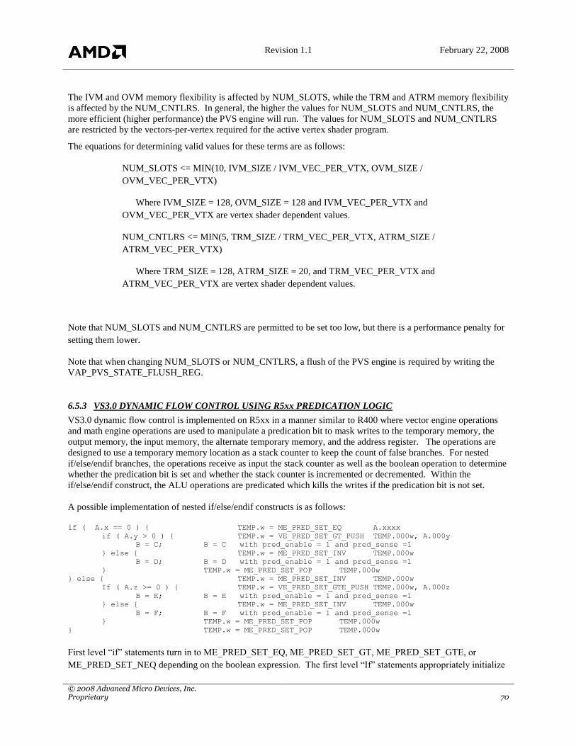
Revision 1.1 February 22, 2008
© 2008 Advanced Micro Devices, Inc. Proprietary 70
The IVM and OVM memory flexibility is affected by NUM_SLOTS, while the TRM and ATRM memory flexibility
is affected by the NUM_CNTLRS. In general, the higher the values for NUM_SLOTS and NUM_CNTLRS, the
more efficient (higher performance) the PVS engine will run. The values for NUM_SLOTS and NUM_CNTLRS
are restricted by the vectors-per-vertex required for the active vertex shader program.
The equations for determining valid values for these terms are as follows:
NUM_SLOTS <= MIN(10, IVM_SIZE / IVM_VEC_PER_VTX, OVM_SIZE /
OVM_VEC_PER_VTX)
Where IVM_SIZE = 128, OVM_SIZE = 128 and IVM_VEC_PER_VTX and
OVM_VEC_PER_VTX are vertex shader dependent values.
NUM_CNTLRS <= MIN(5, TRM_SIZE / TRM_VEC_PER_VTX, ATRM_SIZE /
ATRM_VEC_PER_VTX)
Where TRM_SIZE = 128, ATRM_SIZE = 20, and TRM_VEC_PER_VTX and
ATRM_VEC_PER_VTX are vertex shader dependent values.
Note that NUM_SLOTS and NUM_CNTLRS are permitted to be set too low, but there is a performance penalty for
setting them lower.
Note that when changing NUM_SLOTS or NUM_CNTLRS, a flush of the PVS engine is required by writing the
VAP_PVS_STATE_FLUSH_REG.
6.5.3 VS3.0 DYNAMIC FLOW CONTROL USING R5xx PREDICATION LOGIC
VS3.0 dynamic flow control is implemented on R5xx in a manner similar to R400 where vector engine operations
and math engine operations are used to manipulate a predication bit to mask writes to the temporary memory, the
output memory, the input memory, the alternate temporary memory, and the address register. The operations are
designed to use a temporary memory location as a stack counter to keep the count of false branches. For nested
if/else/endif branches, the operations receive as input the stack counter as well as the boolean operation to determine
whether the predication bit is set and whether the stack counter is incremented or decremented. Within the
if/else/endif construct, the ALU operations are predicated which kills the writes if the predication bit is not set.
A possible implementation of nested if/else/endif constructs is as follows:
if ( A.x == 0 ) { TEMP.w = ME_PRED_SET_EQ A.xxxx
if ( A.y > 0 ) { TEMP.w = VE_PRED_SET_GT_PUSH TEMP.000w, A.000y
B = C; B = C with pred_enable = 1 and pred_sense =1
} else { TEMP.w = ME_PRED_SET_INV TEMP.000w
B = D; B = D with pred_enable = 1 and pred_sense =1
} TEMP.w = ME_PRED_SET_POP TEMP.000w
} else { TEMP.w = ME_PRED_SET_INV TEMP.000w
If ( A.z >= 0 ) { TEMP.w = VE_PRED_SET_GTE_PUSH TEMP.000w, A.000z
B = E; B = E with pred_enable = 1 and pred_sense =1
} else { TEMP.w = ME_PRED_SET_INV TEMP.000w
B = F; B = F with pred_enable = 1 and pred_sense =1
} TEMP.w = ME_PRED_SET_POP TEMP.000w
} TEMP.w = ME_PRED_SET_POP TEMP.000w
First level “if” statements turn in to ME_PRED_SET_EQ, ME_PRED_SET_GT, ME_PRED_SET_GTE, or
ME_PRED_SET_NEQ depending on the boolean expression. The first level “If” statements appropriately initialize

Revision 1.1 February 22, 2008
© 2008 Advanced Micro Devices, Inc. Proprietary 71
the predication bit and false branch counter to 0 or 1 depending on the result of the boolean expression. Second
level or deeper “If” statements turn in to VE_PRED_SET_EQ_PUSH, VE_PRED_SET_GT_PUSH,
VE_PRED_SET_GTE_PUSH, or VE_PRED_SET_NEQ_PUSH. These “If” statements require the false branch
counter as an additional input to determine the final status of the predication bit and the output false branch counter.
For these “If” statements, the predication bit will only be set if the input false branch counter is 0 and the boolean
expression is true. “Else” statements turn into ME_PRED_SET_INV, which also require the false branch counter as
an input and only set the predication bit if this counter is 1. If the input false branch counter is 0, the
ME_PRED_SET_INV sets the output false branch counter to 1 for later nesting and resets the predication bit.
“Endif” statements turn into ME_PRED_SET_POP, which decrement and clamp the false branch counter to 0 if
negative.
The ME_PRED_SET_CLR and ME_PRED_SET_RESTORE operations can be used for loop break statements.
The ME_PRED_SET_CLR resets the predication bit and outputs maximum float to set the false branch counter to
an extremely high number to disable successive operations in a breaked loop. The ME_PRED_SET_RESTORE
operation can be used to restore the predication bit and the false branch counter after exiting a breaked loop.
In the R300 architecture, the best performance is achieved by trying to interlace computations so that an operations
source is not the destination of the preceding operation. In the above example, the false branch stack counter stored
in TEMP.w is a very popular source and destination operand, and R5xx performance would be better optimized by
finding other operations to interlace between them.
6.5.4 VS3.0 PREDICATION AND SIMPLE DYNAMIC FLOW CONTROL USING R5xx CONDITIONAL
OPCODES
In a manner similar to R400, R5xx has conditional moves, writes, or muxes to support VS3.0 predication and simple
dynamic flow control. For predication support in VS3.0, a temporary memory vector can be used in place of a
predication bit. VE_COND_WRITE_EQ, VE_COND_WRITE_GT, VE_COND_WRITE_GTE, and
VE_COND_WRITE_NEQ have two input vector source operands where the first source operand is a conditional
component write mask for the writing of the second source vector into the destination vector. An example of VS3.0
predication being supported with a conditional move or write is as follows:
P = pred_set_gt(A.xyzw,Bxyzw); TEMPxyzw = VE_SET_GREATER_THAN(A.xyzw,Bxyzw);
(P) Cxyzw = Dxyzw; Cxyzw = VE_COND_WRITE_NEQ(TEMPxyzw,Dxyzw);
(!P) Cxyzw = Exyzw; Cxyzw = VE_COND_WRITE_EQ(TEMPxyzw,Exyzw);
Conditional mux opcodes include VE_COND_MUX_EQ, VE_COND_MUX_GT, and VE_COND_MUX_GTE
have three input vector source operands where the first source operand is a component mux select selecting between
the second and third source vectors to write the destination vector. The above example can simplified to the
following:
TEMPxyzw = VE_SET_GREATER_THAN(A.xyzw,Bxyzw);
Cxyzw = VE_COND_MUX_EQ(TEMPxyzw,Exyzw,Dxyzw);
The primary limitation of the conditional mux opcodes is that only two of the three source operands can come from
temporary memory since the temporary memory has only two read ports. A possible solution is using the input
memory as a temporary location for one of the three source operands (the input memory can be written by the vector
and math engine). Also, VE_COND_MUX operations could be reverted into two VE_COND_WRITE
opcoderations as above.
Revision 1.1 February 22, 2008
© 2008 Advanced Micro Devices, Inc. Proprietary 72
6.5.5 PVS FLOW CONTROL CAPABILITY
R300 adds the DX9 support for Vertex Shader Flow control. There are 3 types of flow control instructions: JMP,
LOOP and JSR. Up to 16 total JMP, LOOP, and JSR instructions are allowed for any one shader program.
A JMP is a simple conditional JMP from one instruction to another instruction. Only forward jumps are allowed by
DX9. The hardware is capable of backward jumps, but they are not recommended. There is not actually a
conditional jump in R300, if the Boolean jump bit is not set, the the driver should disable the JMP.
A JSR instruction is a conditional Jump to Subroutine. Similar to the JMP, if the JSR Boolean control is disabled,
the driver should disable the JSR. Upon reaching the activation instruction, (the JSR), a jump is made to the
subroutine label (the jump address). The RET instruction is temporarily “activated” in the HW such that when the
RET instruction is reached, it jumps back to the location specified in the VAP_PVS_FLOW_CNTL_ADDRS#
register.
A LOOP instruction allows a set of instructions to be executed multiple times. Upon reaching the loop start
instruction, the loop count is initialized and the fixed-point loop index register is initialized. The Loop End
instruction address is temporarily “activated” such that when that instruction is reached, the loop count is
decremented, the fixed-point loop index register is incremented (by inc_value) and it jumps back to the location
specified in the VAP_PVS_FLOW_CNTL_ADDRS# register. When loop count is decremented to 0, the
LOOP_END instruction is taken out of the temporarily activated list.
R5xx VS3.0 required the following changes to the PVS flow control capability:
1. Loops and subroutines can be nested up to four levels deep. The official definition is 4 levels of loops and
4 levels of subroutines. The actual R5xx implementation supports 8 total between loops and subroutines
(any combination not to exceed 8). Some special points with regard to loop and subroutine nesting:
o Only the inner-most fixed-point loop index register is accessible for memory addressing.
o The inner-most fixed-point loop index is visible within all nested subroutines.
o The fixed-point loop index is initialized for a loop on the activation address for the loop.
2. R5xx support VS3.0 capability for fixed-point loop index addressing for constant memory, input memory,
output memory and temporary memory. VS3.0 requires support for constant memory, input memory, and
output memory. Address clamping is only provided for constant memory, and therefore shader validation
should verify all fixed-point loop index register addressing is within input, output, or temporary boundaries
for that vertex and loop.
3. R5xx supports VS3.0 capability for the loop repeat construct. The loop repeat is similar to a general loop
except the fixed-point loop index is not initialized at the activation of the loop. The loop repeat inherits the
fixed-point loop index from the above nested loop. Though the init value is not used, the loop step value is
still used for the loop repeat. This enables the possibility for creative dual loop indexing of memories, but
the general VS3.0 functionality would set the step value to 0. Upon loop repeat completion, the original
fixed-point loop index is popped back to its pre-loop repeat value. Loop repeats can be nested and use the
fixed-point loop index under a general loop.
4. R5xx VS3.0 supports 16 flow control instructions. VS3.0 treats flow control instructions in the same
manner as ALU instructions and therefore has a logical maximum of 512 flow control instructions if no
ALU instructions were used. However, the 16 R5xx flow control registers can really equate to
approximately 32 VS3.0 flow control instructions since an R5xx loop instruction includes the loop begin
and the loop end and a R5xx subroutine call includes the call, the subroutine start, and the subroutine
return.
*NOTE: When a loop count is set to 0, the driver must change the loop instruction to a jump instruction to jump
over the loop, since the control flow in the HW is done at the end of the loop.
Details on the language syntax are described below.
Caveats:
Revision 1.1 February 22, 2008
© 2008 Advanced Micro Devices, Inc. Proprietary 73
When a loop count is changed to 0, the driver must change this loop to be a jump to the end-of-loop label.
Jump Instruction
jump b#, labelname;
1. b# is a boolean flow control constant register signified by "b" and "#" can range
from 0 to 15
2. labelname must be defined downstream and terminated with a ":"
3. There are 16 flow control constant registers of 1bit boolean type
4. Jumps are conditional (the jump will only occur if the value in the specified
boolean flow control constant is '1')
Example mul
mad
jump b2, end;
mad
rcp
end:
mul
out
Subroutine Call Instruction
call b#, labelname;
1. b# is a boolean flow control constant register signified by "b" and "#" can range
from 0 to 15
2. labelname must be defined downstream and terminated with a ":"
3. There are 16 flow control constant registers of 1bit boolean type
4. Subroutine calls are conditional (the call will only occur if the value in the
specified flow control constant is non-zero)
5. A subroutine block is defined as the code between the label referenced when called
to the return from subroutine instruction
6. Loop instructions are allowed inside the subroutine block as long as the end of loop
label is also within the same subroutine block
7. Nested subroutines and loops are allowed to a depth of 8 total.
8. A parent fixed-point index is visible through all subroutine nesting.
Example
call b5 normalize;
Return from Subroutine

Revision 1.1 February 22, 2008
© 2008 Advanced Micro Devices, Inc. Proprietary 74
ret;
1. The "ret" instruction is used to indicate the end of a subroutine
Example
normalize:
dp3 r0.w, r0, r0;
rsq r0.w r0.w;
mul r0, r0, r0.w;
ret;
Loop Instruction
loop i#, labelname;
1. i# is an integer flow control constant register signified by "i" and "#" can range from
0 to 15
2. The 'i' register is comprised of three components i#.c loop count (range 0 to 255), i#.i
initial value (range from 0 to 255), and i#.s step value (range from -128 to 127)
which when referenced as i# is an integer scalar defined by i# = i#.i + n*i#.s where n
is the number of times the loop has been traversed The loop value is clamped to be
in the range (–256 – 255) if it over/underflows.
3. For the "loop" instruction, only the first component (initial value) of the "i" register
is used and the i#.s step value is ignored and treated as '1'
4. labelname must be defined downstream and terminated with a ":"
5. The loop will be traversed i#.c times regardless of the i#.i and i#.s values
6. A zero value i#.c loop count is treated as??? so may not be supported (the driver may
be required to preprocess this case to be a jump to the end-of-loop label)
7. Jump instructions are allowed within a loop block as long as the jump target label is
also within the same loop block
8. Jump Subroutine instructions are allowed within a loop block
9. Nested subroutines and loops are allowed to a depth of 8 total.
Example
mul
mad
loop i13, endloop;
mad
mul
endloop:
mul
out
Loop Instruction With Auto-Increment
iloop i#, labelname;
1. i# is an integer flow control constant register signified by "i" and "#" can range from
Revision 1.1 February 22, 2008
© 2008 Advanced Micro Devices, Inc. Proprietary 75
0 to 15
2. The 'i' register is comprised of three components i#.c loop count (range 0 to 255), i#.i
initial value (range from 0 to 255), and i#.s step value (range from -128 to 127)
which when referenced as i# is an integer scalar defined by i# = i#.i + n*i#.s where n
is the number of times the loop has been traversed The loop value is clamped to be
in the range (–256 – 255) if it over/underflows.
3. labelname must be defined downstream and terminated with a ":"
4. The loop will be traversed i#.c times regardless of the i#.i and i#.s values
5. A zero value i#.c loop count is treated as??? so may not be supported (the driver may
be required to preprocess this case to be a jump to the end-of-loop label)
6. Jump instructions are allowed within an iloop block as long as the jump target label
is also within the same iloop block
7. Jump Subroutine instructions are allowed within an iloop block
8. Nested subroutines and loops are allowed to a depth of 8 total.
9. With nested loops, only the inner-most fixed-point loop index is accessible for ALU
source operand addressing. The resulting address is not clamped for the input,
output, and temporary memories so shader validation is required to ensure all
addressing using the fixed-point loop index is within the boundaries for that vertex
and loop.
10. A loop repeat construct does not initialize the fixed-point loop index. The loop
repeat inherits the fixed-point loop index from the above nested loop. Though the
init value is not used, the loop step value is still used for the loop repeat. This
enables the possibility for creative dual loop indexing of memories, but the general
VS3.0 functionality would set the step value to 0. Upon loop repeat completion, the
original fixed-point loop index is popped to its pre-loop repeat value.
Example
mul
mad
iloop i5, endloop;
mul
mad r0, r0, c[i5]; // faster to use loop counter than a0
add
endloop:
mul
out
6.5.6 DUAL MATH OP USAGE
The R300 PVS design enables the ability to use both the Vector Engine and the Math Engine on the same clock. An
instruction which combines a Vector Engine and a Math Engine instruction will be termed a Dual-Math Instruction.
A Dual-Math Instruction has the following restrictions:
The Vector Instruction of a Dual-Math Inst must not use more than 2 source operands because the Math Instruction
definition is stored in the 3rd
source operand bits of the instruction field.

Revision 1.1 February 22, 2008
© 2008 Advanced Micro Devices, Inc. Proprietary 76
The Math Instruction of a Dual-Math Inst must have 2 or less source scalar operands which must both come from a
single source vector. Swizzles enable the two scalar operands to come from any components of the single source
vector.
The Vector Instruction of a Dual-Math Inst cannot have the destination operand use the ATRM memory.
The Math Instruction of a Dual-Math Inst can only use the ATRM memory as the destination operand and can only
write to locations 0-3 and cannot use relative addressing (address register).
The combined instructions source operands must conform to the same memory restrictions as a single op (1 unique
src from CSM, IVM, ATRM, 2 unique src from TRM (3 unique src from TRM only allowed for single op Vector
Macro inst)).
6.5.7 VECTOR INSTRUCTIONS
VE_DOT_PRODUCT: 2 VECTOR SOURCE OPERANDS
OUT.X = ((IN_A.X * IN_B.X) + (IN_A.Y * IN_B.Y)
+ (IN_A.Z * IN_B.Z) + (IN_A.W * IN_B.W));
OUT.Y = OUT.Z = OUT.W = OUT.X
VE_MULTIPLY: 2 VECTOR SOURCE OPERANDS
OUT.X = IN_A.X * IN_B.X;
OUT.Y = IN_A.Y * IN_B.Y;
OUT.Z = IN_A.Z * IN_B.Z;
OUT.W = IN_A.W * IN_B.W;
VE_ADD: 2 VECTOR SOURCE OPERANDS
OUT.X = IN_A.X + IN_B.X;
OUT.Y = IN_A.Y + IN_B.Y;
OUT.Z = IN_A.Z + IN_B.Z;
OUT.W = IN_A.W + IN_B.W;
VE_MULTIPLY_ADD: 3 VECTOR SOURCE OPERANDS (MACRO IF 3 UNIQUE TEMPS)
OUT.X = (IN_A.X * IN_B.X) + IN_C.X;
OUT.Y = (IN_A.Y * IN_B.Y) + IN_C.Y;
OUT.Z = (IN_A.Z * IN_B.Z) + IN_C.Z;
OUT.W = (IN_A.W * IN_B.W) + IN_C.W;
Revision 1.1 February 22, 2008
© 2008 Advanced Micro Devices, Inc. Proprietary 77
VE_DISTANCE_VECTOR: 2 VECTOR SOURCE OPERANDS
OUT.X = 1.0;
OUT.Y = IN_A.Y * IN_B.Y;
OUT.Z = IN_A.Z;
OUT.W = IN_B.W;
Potentially useful as follows (XX = Don‟t Care, D = Depth)
IN_A = (XX, D * D, D * D, XX)
IN_B = (XX, 1 / D, XX, 1 / D)
OUT = (1.0, D, D*D, 1/D) for light attenuation multiply.
VE_FRACTION: 1 VECTOR SOURCE OPERAND
OUT.X = IN_A.X – FLOOR(IN_A.X);
OUT.Y = IN_A.Y – FLOOR(IN_A.Y);
OUT.Z = IN_A.Z – FLOOR(IN_A.Z);
OUT.W = IN_A.W – FLOOR(IN_A.W);
This function returns the positive difference between a floating point number and the
largest integer number less than the floating point number.
VE_MAXIMUM: 2 VECTOR SOURCE OPERANDS
OUT.X = MAX(IN_A.X, IN_B.X);
OUT.Y = MAX(IN_A.Y, IN_B.Y);
OUT.Z = MAX(IN_A.Z, IN_B.Z);
OUT.W = MAX(IN_A.W, IN_B.W);
VE_MINIMUM: 2 VECTOR SOURCE OPERANDS
OUT.X = MIN(IN_A.X, IN_B.X);
OUT.Y = MIN(IN_A.Y, IN_B.Y);
OUT.Z = MIN(IN_A.Z, IN_B.Z);
Revision 1.1 February 22, 2008
© 2008 Advanced Micro Devices, Inc. Proprietary 78
OUT.W = MIN(IN_A.W, IN_B.W);
VE_SET_GREATER_THAN_EQUAL: 2 VECTOR SOURCE OPERANDS
OUT.X = (IN_A.X >= IN_B.X) ? 1.0 : 0.0;
OUT.Y = (IN_A.Y >= IN_B.Y) ? 1.0 : 0.0;
OUT.Z = (IN_A.Z >= IN_B.Z) ? 1.0, 0.0;
OUT.W = (IN_A.W >= IN_B.W) ? 1.0, 0.0;
VE_SET_LESS_THAN: 2 VECTOR SOURCE OPERANDS
OUT.X = (IN_A.X < IN_B.X) ? 1.0, 0.0;
OUT.Y = (IN_A.Y < IN_B.Y) ? 1.0, 0.0;
OUT.Z = (IN_A.Z < IN_B.Z) ? 1.0, 0.0;
OUT.W = (IN_A.W < IN_B.W) ? 1.0, 0.0;
VE_MULTIPLYX2_ADD: 3 VECTOR SOURCE OPERANDS (MACRO IF 3 UNIQUE
TEMPS)
OUT.X = (2.0 * (IN_A.X * IN_B.X)) + IN_C.X;
OUT.Y = (2.0 * (IN_A.Y * IN_B.Y)) + IN_C.Y;
OUT.Z = (2.0 * (IN_A.Z * IN_B.Z)) + IN_C.Z;
OUT.W = (2.0 * (IN_A.W * IN_B.W)) + IN_C.W;
VE_MULTIPLY_CLAMP: 3 VECTOR SOURCE OPERANDS (NO MACRO -> NO 3
UNIQUE TEMPS)
IF(C.W < (A.W * B.W)) {
OUT.X = C.W;
} ELSE IF(C.X >= (A.X * B.X)) {
OUT.X = C.X;
} ELSE {
OUT.X = A.X * B.X;
}
Revision 1.1 February 22, 2008
© 2008 Advanced Micro Devices, Inc. Proprietary 79
OUT.Y = OUT.Z = OUT.W = OUT.X;
This function is used for point sprite clamping. May or may not be useful for other
functions.
VE_FLT2FIX_DX: 1 VECTOR SOURCE OPERAND
OUT.X = FLOOR(IN_A.X);
OUT.Y = FLOOR(IN_A.Y);
OUT.Z = FLOOR(IN_A.Z);
OUT.W = FLOOR(IN_A.W);
This function is a component-wise float to fixed conversion which returns the largest
integer less than the input value. This function is used to load the address register.
VE_FLT2FIX_DX_RND: 1 VECTOR SOURCE OPERAND
OUT.X = FLOOR(IN_A.X + 0.5);
OUT.Y = FLOOR(IN_A.Y + 0.5);
OUT.Z = FLOOR(IN_A.Z + 0.5);
OUT.W = FLOOR(IN_A.W + 0.5);
This function is a component-wise float to fixed conversion which returns the nearest
integer to the input value. This function is used to load the address register.
VE_PRED_SET_EQ_PUSH: 2 VECTOR SOURCE OPERANDS
IF( (IN_B.W==0) && (IN_A.W==0) ) {
PREDICATE_BIT = 1;
OUT.W = 0;
} ELSE {
PREDICATE_BIT = 0;
OUT.W = IN_A.W + 1.0;
}
OUT.X = OUT.Y = OUT.Z = OUT.W;
VE_PRED_SET_GT_PUSH: 2 VECTOR SOURCE OPERANDS
IF( (IN_B.W>0) && (IN_A.W==0) ) {
Revision 1.1 February 22, 2008
© 2008 Advanced Micro Devices, Inc. Proprietary 80
PREDICATE_BIT = 1;
OUT.W = 0;
} ELSE {
PREDICATE_BIT = 0;
OUT.W = IN_A.W + 1.0;
}
OUT.X = OUT.Y = OUT.Z = OUT.W;
VE_PRED_SET_GTE_PUSH: 2 VECTOR SOURCE OPERANDS
IF( (IN_B.W>=0) && (IN_A.W==0) ) {
PREDICATE_BIT = 1;
OUT.W = 0;
} ELSE {
PREDICATE_BIT = 0;
OUT.W = IN_A.W + 1.0;
}
OUT.X = OUT.Y = OUT.Z = OUT.W;
VE_PRED_SET_NEQ_PUSH: 2 VECTOR SOURCE OPERANDS
IF( (IN_B.W!=0) && (IN_A.W==0) ) {
PREDICATE_BIT = 1;
OUT.W = 0;
} ELSE {
PREDICATE_BIT = 0;
OUT.W = IN_A.W + 1.0;
}
OUT.X = OUT.Y = OUT.Z = OUT.W;
VE_COND_WRITE_EQ4 : 2 VECTOR SOURCE OPERANDS
WRITE_ENABLE[0] = ( IN_A.X==0 ) ? 1 : 0;
Revision 1.1 February 22, 2008
© 2008 Advanced Micro Devices, Inc. Proprietary 81
WRITE_ENABLE[1] = ( IN_A.Y==0 ) ? 1 : 0;
WRITE_ENABLE[2] = ( IN_A.Z==0 ) ? 1 : 0;
WRITE_ENABLE[3] = ( IN_A.W==0 ) ? 1 : 0;
OUT = IN_B;
VE_COND_WRITE_GT4 : 2 VECTOR SOURCE OPERANDS
WRITE_ENABLE[0] = ( IN_A.X>0 ) ? 1 : 0;
WRITE_ENABLE[1] = ( IN_A.Y>0 ) ? 1 : 0;
WRITE_ENABLE[2] = ( IN_A.Z>0 ) ? 1 : 0;
WRITE_ENABLE[3] = ( IN_A.W>0 ) ? 1 : 0;
OUT = IN_B;
VE_COND_WRITE_GTE4 : 2 VECTOR SOURCE OPERANDS
WRITE_ENABLE[0] = ( IN_A.X>=0 ) ? 1 : 0;
WRITE_ENABLE[1] = ( IN_A.Y>=0 ) ? 1 : 0;
WRITE_ENABLE[2] = ( IN_A.Z>=0 ) ? 1 : 0;
WRITE_ENABLE[3] = ( IN_A.W>=0 ) ? 1 : 0;
OUT = IN_B;
VE_COND_WRITE_NEQ4 : 2 VECTOR SOURCE OPERANDS
WRITE_ENABLE[0] = ( IN_A.X!=0 ) ? 1 : 0;
WRITE_ENABLE[1] = ( IN_A.Y!=0 ) ? 1 : 0;
WRITE_ENABLE[2] = ( IN_A.Z!=0 ) ? 1 : 0;
WRITE_ENABLE[3] = ( IN_A.W!=0 ) ? 1 : 0;
OUT = IN_B;
VE_COND_MUX_EQ4 : 3 VECTOR SOURCE OPERANDS
// only 2 unique input vectors can be from temporary storage
OUT.X = ( IN_A.X==0 ) ? IN_B.X : IN_C.X;
OUT.Y = ( IN_A.Y==0 ) ? IN_B.Y : IN_C.Y;
OUT.Z = ( IN_A.Z ==0 ) ? IN_B.Z : IN_C.Z;

Revision 1.1 February 22, 2008
© 2008 Advanced Micro Devices, Inc. Proprietary 82
OUT.W = ( IN_A.W==0 ) ? IN_B.W : IN_C.W;
VE_COND_MUX_GT4 : 3 VECTOR SOURCE OPERANDS
// only 2 unique input vectors can be from temporary storage
OUT.X = ( IN_A.X>0 ) ? IN_B.X : IN_C.X;
OUT.Y = ( IN_A.Y>0 ) ? IN_B.Y : IN_C.Y;
OUT.Z = ( IN_A.Z >0 ) ? IN_B.Z : IN_C.Z;
OUT.W = ( IN_A.W>0 ) ? IN_B.W : IN_C.W;
VE_COND_MUX_GTE4 : 3 VECTOR SOURCE OPERANDS
// only 2 unique input vectors can be from temporary storage
OUT.X = ( IN_A.X>=0 ) ? IN_B.X : IN_C.X;
OUT.Y = ( IN_A.Y>=0 ) ? IN_B.Y : IN_C.Y;
OUT.Z = ( IN_A.Z >=0 ) ? IN_B.Z : IN_C.Z;
OUT.W = ( IN_A.W>=0 ) ? IN_B.W : IN_C.W;
VE_SET_GREATER_THAN: 2 VECTOR SOURCE OPERANDS
OUT.X = (IN_A.X > IN_B.X) ? 1.0 : 0.0;
OUT.Y = (IN_A.Y > IN_B.Y) ? 1.0 : 0.0;
OUT.Z = (IN_A.Z > IN_B.Z) ? 1.0, 0.0;
OUT.W = (IN_A.W > IN_B.W) ? 1.0, 0.0;
VE_SET_EQUAL: 2 VECTOR SOURCE OPERANDS
OUT.X = (IN_A.X == IN_B.X) ? 1.0 : 0.0;
OUT.Y = (IN_A.Y== IN_B.Y) ? 1.0 : 0.0;
OUT.Z = (IN_A.Z == IN_B.Z) ? 1.0, 0.0;
OUT.W = (IN_A.W == IN_B.W) ? 1.0, 0.0;
VE_SET_NOT_EQUAL: 2 VECTOR SOURCE OPERANDS
OUT.X = (IN_A.X != IN_B.X) ? 1.0 : 0.0;
OUT.Y = (IN_A.Y != IN_B.Y) ? 1.0 : 0.0;
OUT.Z = (IN_A.Z != IN_B.Z) ? 1.0, 0.0;

Revision 1.1 February 22, 2008
© 2008 Advanced Micro Devices, Inc. Proprietary 83
OUT.W = (IN_A.W != IN_B.W) ? 1.0, 0.0;
NOTES
* A Vector Move Instruction can be accomplished via a VE_ADD with other source operand set to (0,0,0,0).
* A 3-Component Dot Product can be accomplished via a VE_DOT_PRODUCT with 4th
components forced to 0.0.
6.5.8 SCALAR INSTRUCTIONS
The scalar (math) instructions have changed their src operands somewhat for R300. The general rules are as
follows:
1. Only w channels of src operands are available for math ops
2. For all 1 source operand instructions, the input is IN_A.W (except for ME_EXP_BASEE_FF
because of rule 3 below)
3. All source operands which are powers (e^x, 2^x, x^y, etc) will be on IN_C.W, all source operands
which are bases will be on IN_A.W and all sources which are clamps will be on IN_B.W. As long
as the compiler (driver) replicates the last valid src operand to all unused src operands, the
behavior looks clean as follows:
i. 1 source operand instructions (like e^x), the x would be in IN_C.W, but it can appear as
if in IN_A.W as long as this value is replicated
ii. 2 source operand instructions (like x^y), the base is in the IN_A.W, and the pow is in
IN_C.W, but it can appear as if in IN_B.W as long as this value is replicated.
All of the function definitions below are written with the assumption that the last valid source operand is replicated
to the “unused” source operands. The HW does not always use the source operands specified, sometimes it relies on
the replication. These will be noted in comments below.
ME_EXP_BASE2_DX: 1 SCALAR SOURCE OPERAND
OUT.X = 2 ^ FLOOR(IN_A.W);
IF (IN_A.W > 128.0) {
OUT.Y = 0.0; //NOTE: THIS IS NOT EQUIV TO DX BEHAVIOR
} ELSE {
OUT.Y = FRAC(IN_A.W);
}
OUT.Z = 2 ^ (IN_A.W);
OUT.W = 1.0;
ME_LOG_BASE2_DX: 1 SCALAR SOURCE OPERAND
IF(IN_A.W == 0.0) {
OUT.X = MINUS_MAX_FLOAT;

Revision 1.1 February 22, 2008
© 2008 Advanced Micro Devices, Inc. Proprietary 84
OUT.Y = 1.0;
OUT.Z = MINUS_MAX_FLOAT;
OUT.W = 1.0;
} ELSE {
OUT.X = Unbiased exponent of ABS(IN_A.W) as float(i.e. 4.0 -> 2.0);
OUT.Y = mantissa of IN_A.W as float (1.0 <= OUT.Y < 2.0);
OUT.Z = LOG2(ABS(IN_A.W));
OUT.W = 1.0;
}
ME_EXP_BASEE_FF: 1 SCALAR SOURCE OPERAND
OUT.X = e ^ (IN_A.W); //NOTE WAS IN_A.X FOR R200 *FROM C.W, IN_A.W if operand
replicate
OUT.Y = OUT.Z = OUT.W = OUT.X;
ME_LIGHT_COEFF_DX: 3 SCALAR SOURCE OPERANDS (NO MACRO -> NO 3 UNIQUE
TEMPS)
This function was a single vector source operand for R200. Now it uses 3 vector source operands
(w components only).
The 3 operands may be the same vector using different swizzles to emulate R200 behavior.
OUT.X = 1.0;
OUT.Y = MAX(IN_B.W, 0.0);
IF(IN_B.W > 0) {
IN_C.W = CLAMP(IN_C.W, -128.0, 128.0);
OUT.Z = (MAX(IN_A.W, 0.0)) ^ IN_C.W;
} ELSE {
OUT.Z = 0.0;
}
OUT.W = 1.0;
ME_POWER_FUNC_FF: 2 SCALAR SOURCE OPERANDS (IN ONE VECTOR)

Revision 1.1 February 22, 2008
© 2008 Advanced Micro Devices, Inc. Proprietary 85
IF(IN_A.W < 0.0) {
OUT.X = - (ABS(IN_A.W) ^ IN_B.W); //IN_B.W is from IN_C.W, but same if operand
replicate
} ELSE {
OUT.X = IN_A.W ^ IN_B.W;
}
OUT.Y = OUT.Z = OUT.W = OUT.X;
Special cases (in order of detection) are (using x^n notation):
0.0^-n Plus Infinity
0.0^n 0.0
x ^ 0.0 1.0
Inf ^-n 0.0
Inf ^n -> Inf
IF (x >1.0 and n == -Inf) 0.0
IF (x <1.0 and n == -Inf) Inf
IF (x >1.0 and n == Inf) Inf
IF (x <1.0 and n == Inf) 0.0
ME_RECIP_DX: 1 SCALAR SOURCE OPERAND
OUT.X = 1.0 / IN_A.W
OUT.Y = OUT.Z = OUT.W = OUT.X;
An input of 0.0 yields a result of MAX_FLOAT.
ME_RECIP_FF: 1 SCALAR SOURCE OPERAND
OUT.X = 1.0 / IN_A.W
OUT.Y = OUT.Z = OUT.W = OUT.X;
An input of 0.0 yields a result of zero.
ME_RECIP_SQRT_DX: 1 SCALAR SOURCE OPERAND
OUT.X = 1.0 / SQRT(ABS(IN_A.W))
OUT.Y = OUT.Z = OUT.W = OUT.X;

Revision 1.1 February 22, 2008
© 2008 Advanced Micro Devices, Inc. Proprietary 86
An input of 0.0 yields a result of MAX_FLOAT.
ME_RECIP_SQRT_FF: 1 SCALAR SOURCE OPERAND
OUT.X = 1.0 / SQRT(ABS(IN_A.W))
OUT.Y = OUT.Z = OUT.W = OUT.X;
An input of 0.0 yields a result of zero.
ME_MULTIPLY: 2 SCALAR SOURCE OPERANDS (IN ONE VECTOR)
OUT.X = IN_A.W * IN_B.W;
OUT.Y = OUT.Z = OUT.W = OUT.X;
ME_EXP_BASE2: 1 SCALAR SOURCE OPERAND
OUT.X = 2.0 ^ (IN_A.W); //*FROM C.W, IN_A.W if operand replicate
OUT.Y = OUT.Z = OUT.W = OUT.X;
ME_LOG_BASE2: 1 SCALAR SOURCE OPERAND
OUT.X = LOG2(ABS(IN_A.W));
OUT.Y = OUT.Z = OUT.W = OUT.X;
An input of 0.0 yields a result of MINUS_MAX_FLOAT.
ME_POWER_FUNC_FF_CLAMP_B: 3 SCALAR SOURCE OPERANDS (NO MACRO)
IF (IN_A.W < IN_B.W) { //IN_B.W is the clamp value.
OUT.X = 0.0;
} ELSE {
SAME BEHAVIOR AS ME_POWER_FUNC_FF WITH IN_A.W as base and IN_C.W as
power (not IN_B.W).
}
OUT.Y = OUT.Z = OUT.W = OUT.X;
ME_POWER_FUNC_FF_CLAMP_B1: 3 SCALAR SOURCE OPERANDS (NO MACRO)
IF (IN_A.W < IN_B.W) { //IN_B.W is the clamp value.
OUT.X = 0.0;
} ELSE IF (IN_A.W > 1.0) {
Revision 1.1 February 22, 2008
© 2008 Advanced Micro Devices, Inc. Proprietary 87
OUT.X = 1.0;
} ELSE {
SAME BEHAVIOR AS ME_POWER_FUNC_FF WITH IN_A.W as base and IN_C.W as
power (not IN_B.W).
}
OUT.Y = OUT.Z = OUT.W = OUT.X;
ME_POWER_FUNC_FF_CLAMP_01: 2 SCALAR SOURCE OPERANDS
IF (IN_A.W <= 0.0) {
OUT.X = 0.0;
} ELSE IF (IN_A.W > 1.0) {
OUT.X = 1.0;
} ELSE {
SAME BEHAVIOR AS ME_POWER_FUNC_FF
}
OUT.Y = OUT.Z = OUT.W = OUT.X;
ME_SIN: 1 SCALAR SOURCE OPERAND
OUT.X = SIN(IN_A.W);
OUT.Y = OUT.Z = OUT.W = OUT.X;
The hardware implementation of SIN/COS clamps the input, including nans and infs, to -pi to +pi
before computing the output, so for any inputs outside that range, cos(x) = -1 and sin(x) = 0. Except
for inputs of zero where sin(0) = 0, the minimum value that this function will output is +/-
0x33800000. In other words, the absolute value of the output is clamped to 0x33800000 minimum
except for sin(0) and sin(+/-pi).
ME_COS: 1 SCALAR SOURCE OPERAND
OUT.X = COS(IN_A.W);
OUT.Y = OUT.Z = OUT.W = OUT.X;
The hardware implementation of SIN/COS clamps the input, including nans and infs, to -pi to +pi
before computing the output, so for any inputs outside that range, cos(x) = -1 and sin(x) = 0. Except
for inputs of zero where sin(0) = 0, the minimum value that this function will output is +/-
0x33800000. In other words, the absolute value of the output is clamped to 0x33800000 minimum
except for sin(0) and sin(+/-pi).
ME_LOG_BASE2_IEEE: 1 SCALAR SOURCE OPERAND

Revision 1.1 February 22, 2008
© 2008 Advanced Micro Devices, Inc. Proprietary 88
OUT.X = LOG2(ABS(IN_A.W));
OUT.Y = OUT.Z = OUT.W = OUT.X;
An input of 0.0 yields a result of minus infinity.
ME_RECIP_IEEE: 1 SCALAR SOURCE OPERAND
OUT.X = 1.0 / IN_A.W
OUT.Y = OUT.Z = OUT.W = OUT.X;
An input of 0.0 yields a result of infinity.
ME_RECIP_SQRT_IEEE: 1 SCALAR SOURCE OPERAND
OUT.X = 1.0 / SQRT(ABS(IN_A.W))
OUT.Y = OUT.Z = OUT.W = OUT.X;
An input of 0.0 yields a result of infinity.
ME_PRED_SET_EQ: 1 SCALAR SOURCE OPERAND
IF(IN_A.W==0) {
PREDICATE_BIT = 1;
OUT.X = OUT.Y = OUT.Z = OUT.W = 0;
} ELSE {
PREDICATE_BIT = 0;
OUT.X = OUT.Y = OUT.Z = OUT.W = 1;
}
ME_PRED_SET_GT: 1 SCALAR SOURCE OPERAND
IF(IN_A.W > 0) {
PREDICATE_BIT = 1;
OUT.X = OUT.Y = OUT.Z = OUT.W = 0;
} ELSE {
PREDICATE_BIT = 0;
OUT.X = OUT.Y = OUT.Z = OUT.W = 1;
}
Revision 1.1 February 22, 2008
© 2008 Advanced Micro Devices, Inc. Proprietary 89
ME_PRED_SET_GTE: 1 SCALAR SOURCE OPERAND
IF(IN_A.W >= 0) {
PREDICATE_BIT = 1;
OUT.X = OUT.Y = OUT.Z = OUT.W = 0;
} ELSE {
PREDICATE_BIT = 0;
OUT.X = OUT.Y = OUT.Z = OUT.W = 1;
}
ME_PRED_SET_NEQ: 1 SCALAR SOURCE OPERAND
IF(IN_A.W != 0) {
PREDICATE_BIT = 1;
OUT.X = OUT.Y = OUT.Z = OUT.W = 0;
} ELSE {
PREDICATE_BIT = 0;
OUT.X = OUT.Y = OUT.Z = OUT.W = 1;
}
ME_PRED_SET_CLR: 0 SCALAR SOURCE OPERANDS
PREDICATE_BIT = 1;
OUT.X = OUT.Y = OUT.Z = OUT.W = MAX_FLOAT;
ME_PRED_SET_INV: 1 SCALAR SOURCE OPERAND
IF(IN_A.W==1) {
PREDICATE_BIT = 1;
OUT.X = OUT.Y = OUT.Z = OUT.W = 0;
} ELSE {
PREDICATE_BIT = 0;
IF(IN_A.W==0) {
OUT.X = OUT.Y = OUT.Z = OUT.W = 1;

Revision 1.1 February 22, 2008
© 2008 Advanced Micro Devices, Inc. Proprietary 90
} ELSE {
OUT.X = OUT.Y = OUT.Z = OUT.W = IN_A.W;
}
}
ME_PRED_SET_POP: 1 SCALAR SOURCE OPERAND
OUT.W = IN_A.W – 1.0;
IF(OUT.W < 0) {
PREDICATE_BIT = 1;
OUT.W = 0;
} ELSE {
PREDICATE_BIT = 0;
}
OUT.X = OUT.Y = OUT.Z = OUT.W;
ME_PRED_SET_RESTORE: 1 SCALAR SOURCE OPERAND
IF(IN_A.W==0) {
PREDICATE_BIT = 1;
OUT.X = OUT.Y = OUT.Z = OUT.W = 0;
} ELSE {
PREDICATE_BIT = 0;
OUT.X = OUT.Y = OUT.Z = OUT.W = IN_A.W;
}
6.5.9 PVS INSTRUCTION DEFINITION
The memory selects (or register type) valid selections are as follows:
SOURCE REG_TYPES:
PVS_SRC_REG_TEMPORARY = 0; //Intermediate storage
PVS_SRC_REG_INPUT = 1; //Input Vertex Storage

Revision 1.1 February 22, 2008
© 2008 Advanced Micro Devices, Inc. Proprietary 91
PVS_SRC_REG_CONSTANT = 2; //Constant State Storage
PVS_SRC_REG_ALT_TEMPORARY = 3; //Alternate Intermediate Storage
The valid swizzle selects are as follows:
PVS_SRC_SELECT_X = 0; //Select X Component
PVS_SRC_SELECT_Y = 1; //Select Y Component
PVS_SRC_SELECT_Z = 2; //Select Z Component
PVS_SRC_SELECT_W = 3; //Select W Component
PVS_SRC_SELECT_FORCE_0 = 4; //Force Component to 0.0
PVS_SRC_SELECT_FORCE_1 = 5; //Force Component to 1.0
For R5xx VS3.0, the PVS_SRC_ABS_XYZW bits enables the absolute value for the four components of the source
vector.
For R5xx VS3.0, the PVS_DST_VE_SAT and PVS_DST_ME_SAT bits enable a zero to one saturate clamp for all
four component of the output.
For R5xx VS3.0, the PVS_DST_PRED_ENABLE and PVS_DST_PRED_SENSE bits enable predicated writes for
the temporary memory, the output memory, the alternate temporary memory, the address register, and the input
memory. The PVS_DST_PRED_ENABLE enables the feature while PVS_DST_PRED_SENSE determines the
polarity of the predication bit for the write to be enabled. When the predication bit matches the predication sense,
the predicated write is enabled. For dual vector/math engine operations, both operations are predicated.
The PVS_DST_MACRO_INST bit was meant to be used for MACROS such as a vector-matrix multiply, but
currently is only set for the following cases:
A VE_MULTIPLY_ADD or VE_MULTIPLYX2_ADD instruction with all 3 source operands using
unique PVS_REG_TEMPORARY vector addresses. Since R300 only has two read ports on the temporary
memory, this special case of these instructions is broken up (by the HW) into 2 operations.
When the MACRO enable bit is set, the opcode (lower 6 bits is remapped as follows:
PVS_MACRO_OP_2CLK_MADD = 0
PVS_MACRO_OP_2CLK_M2X_ADD = 1
The PVS_DST_MATH_INST is used to identify whether the instruction is a Vector Engine instruction or a Math
Engine instruction.
The PVS_DST_OPCODE values are listed below:
VECTOR_NO_OP = 0
VE_DOT_PRODUCT = 1

Revision 1.1 February 22, 2008
© 2008 Advanced Micro Devices, Inc. Proprietary 92
VE_MULTIPLY = 2
VE_ADD = 3
VE_MULTIPLY_ADD = 4
VE_DISTANCE_VECTOR = 5
VE_FRACTION = 6
VE_MAXIMUM = 7
VE_MINIMUM = 8
VE_SET_GREATER_THAN_EQUAL = 9
VE_SET_LESS_THAN = 10
VE_MULTIPLYX2_ADD = 11
VE_MULTIPLY_CLAMP = 12
VE_FLT2FIX_DX = 13
VE_FLT2FIX_DX_RND = 14
// NEW R5xx OPCODES - below
VE_PRED_SET_EQ_PUSH = 15
VE_PRED_SET_GT_PUSH = 16
VE_PRED_SET_GTE_PUSH = 17
VE_PRED_SET_NEQ_PUSH = 18
VE_COND_WRITE_EQ = 19
VE_COND_WRITE_GT = 20
VE_COND_WRITE_GTE = 21
VE_COND_WRITE_NEQ = 22
VE_COND_MUX_EQ = 23
VE_COND_MUX_GT = 24
VE_COND_MUX_GTE = 25
VE_SET_GREATER_THAN = 26
VE_SET_EQUAL = 27
VE_SET_NOT_EQUAL = 28
MATH_NO_OP = 0
ME_EXP_BASE2_DX = 1
ME_LOG_BASE2_DX = 2
ME_EXP_BASEE_FF = 3
ME_LIGHT_COEFF_DX = 4
ME_POWER_FUNC_FF = 5
ME_RECIP_DX = 6
ME_RECIP_FF = 7
ME_RECIP_SQRT_DX = 8
ME_RECIP_SQRT_FF = 9
ME_MULTIPLY = 10
ME_EXP_BASE2_FULL_DX = 11
ME_LOG_BASE2_FULL_DX = 12
ME_POWER_FUNC_FF_CLAMP_B = 13
ME_POWER_FUNC_FF_CLAMP_B1 = 14
ME_POWER_FUNC_FF_CLAMP_01 = 15
ME_SIN = 16
ME_COS = 17
// NEW R5xx OPCODES - below
ME_LOG_BASE2_IEEE = 18
ME_RECIP_IEEE = 19
ME_RECIP_SQRT_IEEE = 20
ME_PRED_SET_EQ = 21
ME_PRED_SET_GT = 22
ME_PRED_SET_GTE = 23
Revision 1.1 February 22, 2008
© 2008 Advanced Micro Devices, Inc. Proprietary 93
ME_PRED_SET_NEQ = 24
ME_PRED_SET_CLR = 25
ME_PRED_SET_INV = 26
ME_PRED_SET_POP = 27
ME_PRED_SET_RESTORE = 28
DEST REG_TYPES:
PVS_DST_REG_TEMPORARY = 0; //Intermediate storage
PVS_DST_REG_A0 = 1; //Address Register Storage
PVS_DST_REG_OUT = 2; //Output Memory. Used for all outputs
PVS_DST_REG_OUT_REPL_X = 3; //Output Memory & Replicate X to all channels
PVS_DST_REG_ALT_TEMPORARY = 4; //Alternate Intermediate Storage
PVS_DST_REG_INPUT = 5; //Output Memory & Replicate X to all channels
The PVS_REG_A0 may only be used as the destination operand register type when using the VE_FLT2FIX_DX or
the VE_FLT2FIX_DX_RND opcodes.
For R300, PVS_REG_OUT_* is replaced by the single PVS_REG_OUT and the PVS_DST_OFFSET field will be
used to place data in the appropriate vectors. This allows the PVS Output Vertex memories to be variable format for
the variable vertex methodology. The PVS_REG_OUT_REPL_X is equivalent to PVS_REG_OUT except that it
forces the X channel to be replicated onto all 4 output channels. This capability is used to allow the mapping of
Point-Sprite and Discrete Fog to any output memory channel from an instruction with a unique x-channel output.
The PVS_DST_DUAL_MATH_OP bit must be set when combining Vector and Math Engine operations.
The PVS_DST_ADDR_MODE and DST_ADDR_SEL are the same as the SRC operand definitions.
The PVS_DST_OPCODE_MSB is the most significant bit of the PVS_DST_OPCODE field to be used for the math
engine for dual ops. This enables math engine operations 16 through 28 to be used during dual ops.
For R5xx VS3.0, a PVS_SRC_ABS_XYZW bits enables the absolute value for the two components of the dual op
math engine source vector.

Revision 1.1 February 22, 2008
© 2008 Advanced Micro Devices, Inc. Proprietary 94
7. Fragment Shaders
7.1 Introduction
This section describes the functional behavior of the Universal Shaders of on R5xx.
7.2 Instructions
There are 512 instruction slots. A program can begin execution at any address. In the absence of flow control,
programs will increment the program counter after each instruction. The program counter wraps at 512
automatically, so it is valid to load shader programs which utilize the bottommost and topmost regions of the
instruction store.
Each instruction can be one of four types:
US_INST_TYPE_ALU Arithmetic and Logic Unit instruction
US_INST_TYPE_OUTPUT Output instruction (with ALU functionality)
US_INST_TYPE_FC Flow Control instruction
US_INST_TYPE_TEX Texture instruction
ALU and OUTPUT instructions both have full RGB and Alpha math functionality. The only functional difference
between them is that ALU instructions can set the predicate bits, and OUTPUT instructions can write to the output
registers. There is no way to do both in the same instruction. Internally, the sequencer must treat instructions that
have potential outputs specially for scheduling. The last executed instruction of the shader program must also be an
OUTPUT instruction, even if it's not outputting anything interesting.
The first OUTPUT instruction will reserve space in the output register fifo. This space is limited, therefore issuing
an OUTPUT earlier than necessary may cause threads to stall earlier than necessary. You should not set an ALU
instruction as type OUTPUT unless it is actually writing to an output register, or it is the last instruction of the
program.
Flow control instructions and texture instructions each have their own interpretation of the bits in the instruction
word.
The active shader should reside in the range US_CODE_RANGE.CODE_ADDR to
US_CODE_RANGE.CODE_ADDR + US_CODE_RANGE.CODE_SIZE, inclusive (note that
US_CODE_RANGE.CODE_SIZE is the size of the shader program, minus one). You may setup additional shaders
in advance outside of this range, but the current shader should not attempt to execute code outside of this range.
The shader has an offset, US_CODE_OFFSET.OFFSET_ADDR, associated with it that is added to various
instruction addresses, minimizing the number of registers you may need to update when relocating a shader. Each
pixel starts the shader at instruction US_CODE_ADDR.START_ADDR + US_CODE_OFFSET.OFFSET_ADDR
(instruction addresses are always modulo 512). Execution continues until the program counter reaches
US_CODE_SIZE.END_ADDR + US_CODE_OFFSET.OFFSET_ADDR. It does not matter how many pixels in
the group are active (even none), the program will end after that instruction is executed. The instruction at the end

Revision 1.1 February 22, 2008
© 2008 Advanced Micro Devices, Inc. Proprietary 95
address must be an OUTPUT instruction (even if the output mask is zero), and should always wait for the texture
unit semaphore by setting the TEX_SEM_WAIT bit (see below). At the time of termination, the contents of the
output registers are sent to the render targets.
Multiple shaders can be loaded into the instruction memory. Switching between them only requires changing global
registers like US_CODE_ADDR, US_CODE_RANGE, US_CODE_OFFSET, US_PIXSIZE, and US_FC_CTRL.
Updates to shader code outside the currently active program are safe, and do not stall the pipeline. If you intend to
overwrite the active shader, however, the pixel shader pipe must be flushed so that pixels running the old shader get
out before the update. Register writes to US_CODE_ADDR, US_CODE_RANGE, US_CODE_OFFSET, and/or
US_PIXSIZE should flush the pixel shader pipe.
The US instruction and ALU constant registers cannot be written to directly, due to addressing limitations elsewhere
in the pipe. A vector mechanism is provided in the GA block for writing to the US registers. Details on writing the
US registers are provided toward the end of this document.
7.3 Instruction Words
US_INST_TYPE_ALU / US_INST_TYPE_OUTPUT (6 registers):
US_CMN_INST_*
US_ALU_RGB_ADDR_*
US_ALU_ALPHA_ADDR_*
US_ALU_RGB_INST_*
US_ALU_ALPHA_INST_*
US_ALU_RGBA_INST_*
US_INST_TYPE_FC (3 registers):
US_CMN_INST_*
US_FC_INST_*
US_FC_ADDR_*
US_INST_TYPE_TEX (4 registers):
US_CMN_INST_*
US_TEX_INST_*
US_TEX_ADDR_*
US_TEX_ADDR_DXDY_*
The FC and TEX words overlap with the ALU/OUTPUT words in instruction memory. The unused memory
locations for FC and TEX are ignored by US; they may be left uninitialized, or set to zero, with no ill effect.
However, the driver should take care to write to all registers that are required by each instruction type.
Within US_CMN_INST_*, the fields effective for each instruction type are indicated by *s:
ALU OUTPUT FC TEX
TYPE * * * *
TEX_SEM_WAIT * * * *
RGB_PRED_SEL * * * *
RGB_PRED_INV * * * *
ALPHA_PRED_SEL * * *
ALPHA_PRED_INV * * *

Revision 1.1 February 22, 2008
© 2008 Advanced Micro Devices, Inc. Proprietary 96
WRITE_INACTIVE * * *
LAST * * * *
NOP * *
RGB_WMASK * * *
ALPHA_WMASK * * *
RGB_OMASK * *
ALPHA_OMASK * *
RGB_CLAMP * *
ALPHA_CLAMP * *
ALU_RESULT_SEL * *
ALU_RESULT_OP * *
ALU_WAIT * *
STAT_WE * * *
7.3.1 Synchronization of instruction streams
The US allows you to freely intermix instructions of multiple types. It will process the three types (ALU/Output,
Texture, and FC) in parallel whenever possible. Instructions need to be synchronized when an instruction of one
type depends on the output of another type. The cases where explicit synchronization may be required are:
TEX instruction dependent on ALU for source register or predicate. Synchronized with the ALU_WAIT
bit.
FC instruction dependent on ALU for predicate or ALU result. Synchronized with the ALU_WAIT bit.
ALU instruction dependent on TEX for lookup result. Synchronized using the texture semaphore.
A texture or FC instruction that uses a result computed by a prior ALU instruction should set the ALU_WAIT bit.
This forces processing for the thread to stall until pending ALU instructions are complete. A latency of about 30
cycles is imposed on the thread.
Note that a static FC instruction never needs to set ALU_WAIT since it never depends on a result computed within
the shader. Also, an ALU instruction never needs to set ALU_WAIT -- dependencies amongst ALU instructions are
resolved internally.
The texture semaphore is used to synchronize the output of a texture instruction with a subsequent ALU or texture
instruction that uses that result. Since the latency for a texture fetch is difficult to anticipate in advance, the texture
semaphore mechanism is more complex than ALU_WAIT. The texture semaphore is described in more detail
below.
7.4 ALU Instructions
An ALU instruction actually consists of an RGB vector instruction and an Alpha scalar instruction.
There are only a few operations that only one or the other unit can compute, but in each case there is a special
instruction the other engine can use to copy the result.
7.4.1 Sources
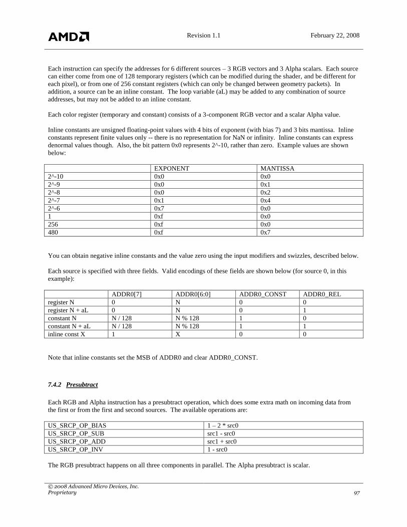
Revision 1.1 February 22, 2008
© 2008 Advanced Micro Devices, Inc. Proprietary 97
Each instruction can specify the addresses for 6 different sources – 3 RGB vectors and 3 Alpha scalars. Each source
can either come from one of 128 temporary registers (which can be modified during the shader, and be different for
each pixel), or from one of 256 constant registers (which can only be changed between geometry packets). In
addition, a source can be an inline constant. The loop variable (aL) may be added to any combination of source
addresses, but may not be added to an inline constant.
Each color register (temporary and constant) consists of a 3-component RGB vector and a scalar Alpha value.
Inline constants are unsigned floating-point values with 4 bits of exponent (with bias 7) and 3 bits mantissa. Inline
constants represent finite values only -- there is no representation for NaN or infinity. Inline constants can express
denormal values though. Also, the bit pattern 0x0 represents 2^-10, rather than zero. Example values are shown
below:
EXPONENT MANTISSA
2^-10 0x0 0x0
2^-9 0x0 0x1
2^-8 0x0 0x2
2^-7 0x1 0x4
2^-6 0x7 0x0
1 0xf 0x0
256 0xf 0x0
480 0xf 0x7
You can obtain negative inline constants and the value zero using the input modifiers and swizzles, described below.
Each source is specified with three fields. Valid encodings of these fields are shown below (for source 0, in this
example):
ADDR0[7] ADDR0[6:0] ADDR0_CONST ADDR0_REL
register N 0 N 0 0
register N + aL 0 N 0 1
constant N N / 128 N % 128 1 0
constant N + aL N / 128 N % 128 1 1
inline const X 1 X 0 0
Note that inline constants set the MSB of ADDR0 and clear ADDR0_CONST.
7.4.2 Presubtract
Each RGB and Alpha instruction has a presubtract operation, which does some extra math on incoming data from
the first or from the first and second sources. The available operations are:
US_SRCP_OP_BIAS 1 – 2 * src0
US_SRCP_OP_SUB src1 - src0
US_SRCP_OP_ADD src1 + src0
US_SRCP_OP_INV 1 - src0
The RGB presubtract happens on all three components in parallel. The Alpha presubtract is scalar.

Revision 1.1 February 22, 2008
© 2008 Advanced Micro Devices, Inc. Proprietary 98
If any presubtract result is used in the instruction, and one of the sources being used in a presubtract is written in the
previous instruction, and the previous instruction is an ALU or output instruction, a NOP needs to be inserted
between the two instructions. Do this by setting the NOP flag in the previous instruction, so the NOP does not
consume an instruction slot. This allows the HW the extra cycle necessary to resolve the dependencies involved in
doing this extra math (there are additional cases where NOP may need to be set, noted below).
NOP is never required if the previous instruction is a texture lookup.
7.4.3 Inputs
Each math operation has zero to three inputs. Each input can be configured to select a source and swizzle its
channels. There are fields to configure 6 inputs per instruction: 3 for RGB and 3 for Alpha. An instruction can read
in at most 12 independent colour components (9 RGB components and 3 alpha components).
7.4.3.1 Select
Each input selects from src0, src1, src2, or the presubtract result ("srcp"). One can conceive of the selects
assembling a 4-component vector as seen below. The swizzle selects (see next section) determine which of the four
values are chosen to actually take part in the computations.
{ rgb_addr0->r
src0 ={ rgb_addr0->g
{ rgb_addr0->b
{ alpha_addr0->a
{ rgb_addr1->r
src1 ={ rgb_addr1->g
{ rgb_addr1->b
{ alpha_addr1->a
{ rgb_addr2->r
src2 ={ rgb_addr2->g
{ rgb_addr2->b
{ alpha_addr2->a
{ rgb_srcp_result.r = rgb_srcp_op(rgb_addr0->r, rgb_addr1->r)
srcp ={ rgb_srcp_result.g = rgb_srcp_op(rgb_addr0->g, rgb_addr1->g)
{ rgb_srcp_result.b = rgb_srcp_op(rgb_addr0->b, rgb_addr1->b)
{ alpha_srcp_result.a = alpha_srcp_op(alpha_addr0->a, alpha_addr1->a)
The RGB and alpha units each take three operands, A, B, and C. These operands are selected with the RGB_SEL_x
and ALPHA_SEL_x fields. Note that src0, src1 and src2 are fetched from a combination of the RGB and alpha
source addresses. If the RGB unit swizzles in an alpha component, the alpha component will always come from
alpha_addr*. Similarly, if the alpha unit swizzles in an RGB component, it will always come from rgb_addr*.
7.4.3.2 Swizzle
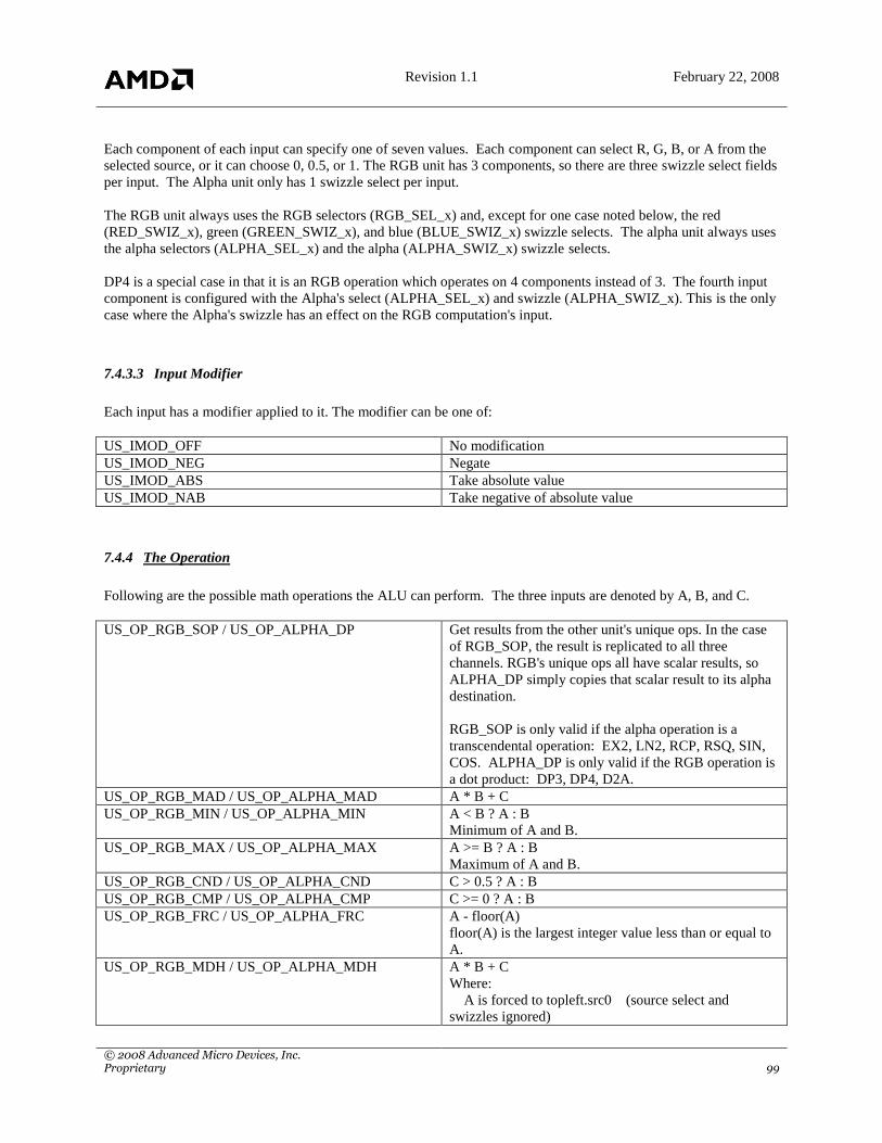
Revision 1.1 February 22, 2008
© 2008 Advanced Micro Devices, Inc. Proprietary 99
Each component of each input can specify one of seven values. Each component can select R, G, B, or A from the
selected source, or it can choose 0, 0.5, or 1. The RGB unit has 3 components, so there are three swizzle select fields
per input. The Alpha unit only has 1 swizzle select per input.
The RGB unit always uses the RGB selectors (RGB_SEL_x) and, except for one case noted below, the red
(RED_SWIZ_x), green (GREEN_SWIZ_x), and blue (BLUE_SWIZ_x) swizzle selects. The alpha unit always uses
the alpha selectors (ALPHA_SEL_x) and the alpha (ALPHA_SWIZ_x) swizzle selects.
DP4 is a special case in that it is an RGB operation which operates on 4 components instead of 3. The fourth input
component is configured with the Alpha's select (ALPHA_SEL_x) and swizzle (ALPHA_SWIZ_x). This is the only
case where the Alpha's swizzle has an effect on the RGB computation's input.
7.4.3.3 Input Modifier
Each input has a modifier applied to it. The modifier can be one of:
US_IMOD_OFF No modification
US_IMOD_NEG Negate
US_IMOD_ABS Take absolute value
US_IMOD_NAB Take negative of absolute value
7.4.4 The Operation
Following are the possible math operations the ALU can perform. The three inputs are denoted by A, B, and C.
US_OP_RGB_SOP / US_OP_ALPHA_DP Get results from the other unit's unique ops. In the case
of RGB_SOP, the result is replicated to all three
channels. RGB's unique ops all have scalar results, so
ALPHA_DP simply copies that scalar result to its alpha
destination.
RGB_SOP is only valid if the alpha operation is a
transcendental operation: EX2, LN2, RCP, RSQ, SIN,
COS. ALPHA_DP is only valid if the RGB operation is
a dot product: DP3, DP4, D2A.
US_OP_RGB_MAD / US_OP_ALPHA_MAD A * B + C
US_OP_RGB_MIN / US_OP_ALPHA_MIN A < B ? A : B
Minimum of A and B.
US_OP_RGB_MAX / US_OP_ALPHA_MAX A >= B ? A : B
Maximum of A and B.
US_OP_RGB_CND / US_OP_ALPHA_CND C > 0.5 ? A : B
US_OP_RGB_CMP / US_OP_ALPHA_CMP C >= 0 ? A : B
US_OP_RGB_FRC / US_OP_ALPHA_FRC A - floor(A)
floor(A) is the largest integer value less than or equal to
A.
US_OP_RGB_MDH / US_OP_ALPHA_MDH A * B + C
Where:
A is forced to topleft.src0 (source select and
swizzles ignored)
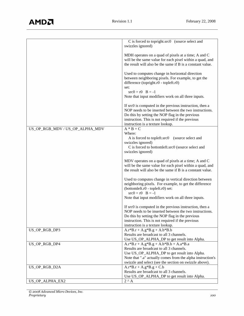
Revision 1.1 February 22, 2008
© 2008 Advanced Micro Devices, Inc. Proprietary 100
C is forced to topright.src0 (source select and
swizzles ignored)
MDH operates on a quad of pixels at a time; A and C
will be the same value for each pixel within a quad, and
the result will also be the same if B is a constant value.
Used to computes change in horizontal direction
between neighboring pixels. For example, to get the
difference (topright.r0 - topleft.r0)
set:
src0 = r0 B = -1
Note that input modifiers work on all three inputs.
If src0 is computed in the previous instruction, then a
NOP needs to be inserted between the two instructions.
Do this by setting the NOP flag in the previous
instruction. This is not required if the previous
instruction is a texture lookup.
US_OP_RGB_MDV / US_OP_ALPHA_MDV A * B + C
Where:
A is forced to topleft.src0 (source select and
swizzles ignored)
C is forced to bottomleft.src0 (source select and
swizzles ignored)
MDV operates on a quad of pixels at a time; A and C
will be the same value for each pixel within a quad, and
the result will also be the same if B is a constant value.
Used to computes change in vertical direction between
neighboring pixels. For example, to get the difference
(bottomleft.r0 - topleft.r0) set:
src0 = r0 B = -1
Note that input modifiers work on all three inputs.
If src0 is computed in the previous instruction, then a
NOP needs to be inserted between the two instructions.
Do this by setting the NOP flag in the previous
instruction. This is not required if the previous
instruction is a texture lookup.
US_OP_RGB_DP3 A.r*B.r + A.g*B.g + A.b*B.b
Results are broadcast to all 3 channels.
Use US_OP_ALPHA_DP to get result into Alpha.
US_OP_RGB_DP4 A.r*B.r + A.g*B.g + A.b*B.b + A.a*B.a
Results are broadcast to all 3 channels.
Use US_OP_ALPHA_DP to get result into Alpha.
Note that ".a" actually comes from the alpha instruction's
swizzle and select (see the section on swizzle above).
US_OP_RGB_D2A A.r*B.r + A.g*B.g + C.b
Results are broadcast to all 3 channels.
Use US_OP_ALPHA_DP to get result into Alpha.
US_OP_ALPHA_EX2 2 ^ A
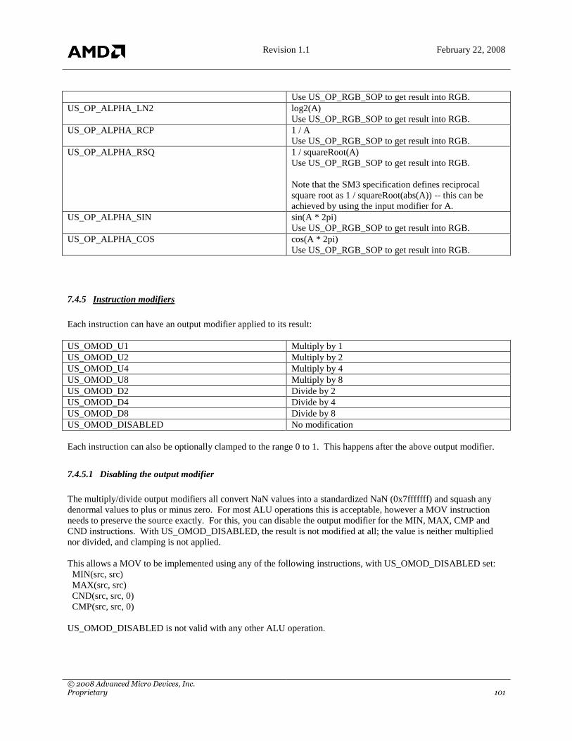
Revision 1.1 February 22, 2008
© 2008 Advanced Micro Devices, Inc. Proprietary 101
Use US_OP_RGB_SOP to get result into RGB.
US_OP_ALPHA_LN2 log2(A)
Use US_OP_RGB_SOP to get result into RGB.
US_OP_ALPHA_RCP 1 / A
Use US_OP_RGB_SOP to get result into RGB.
US_OP_ALPHA_RSQ 1 / squareRoot(A)
Use US_OP_RGB_SOP to get result into RGB.
Note that the SM3 specification defines reciprocal
square root as 1 / squareRoot(abs(A)) -- this can be
achieved by using the input modifier for A.
US_OP_ALPHA_SIN sin(A * 2pi)
Use US_OP_RGB_SOP to get result into RGB.
US_OP_ALPHA_COS cos(A * 2pi)
Use US_OP_RGB_SOP to get result into RGB.
7.4.5 Instruction modifiers
Each instruction can have an output modifier applied to its result:
US_OMOD_U1 Multiply by 1
US_OMOD_U2 Multiply by 2
US_OMOD_U4 Multiply by 4
US_OMOD_U8 Multiply by 8
US_OMOD_D2 Divide by 2
US_OMOD_D4 Divide by 4
US_OMOD_D8 Divide by 8
US_OMOD_DISABLED No modification
Each instruction can also be optionally clamped to the range 0 to 1. This happens after the above output modifier.
7.4.5.1 Disabling the output modifier
The multiply/divide output modifiers all convert NaN values into a standardized NaN (0x7fffffff) and squash any
denormal values to plus or minus zero. For most ALU operations this is acceptable, however a MOV instruction
needs to preserve the source exactly. For this, you can disable the output modifier for the MIN, MAX, CMP and
CND instructions. With US_OMOD_DISABLED, the result is not modified at all; the value is neither multiplied
nor divided, and clamping is not applied.
This allows a MOV to be implemented using any of the following instructions, with US_OMOD_DISABLED set:
MIN(src, src)
MAX(src, src)
CND(src, src, 0)
CMP(src, src, 0)
US_OMOD_DISABLED is not valid with any other ALU operation.
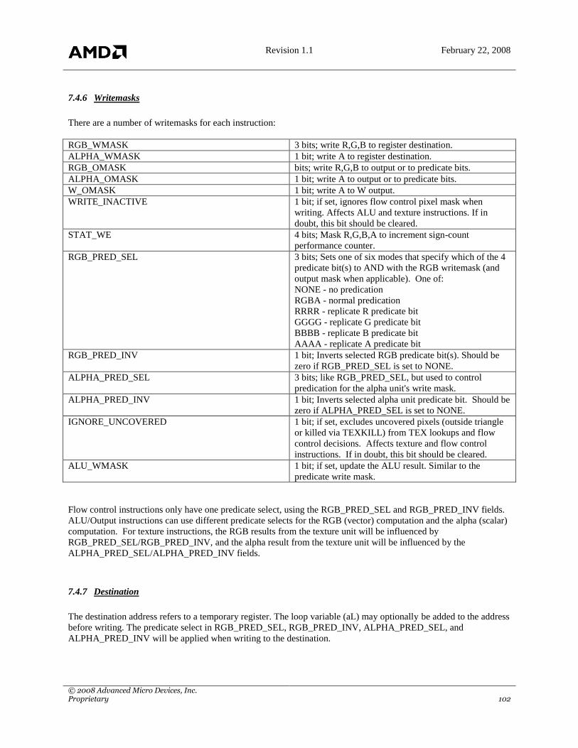
Revision 1.1 February 22, 2008
© 2008 Advanced Micro Devices, Inc. Proprietary 102
7.4.6 Writemasks
There are a number of writemasks for each instruction:
RGB_WMASK 3 bits; write R,G,B to register destination.
ALPHA_WMASK 1 bit; write A to register destination.
RGB_OMASK bits; write R,G,B to output or to predicate bits.
ALPHA_OMASK 1 bit; write A to output or to predicate bits.
W_OMASK 1 bit; write A to W output.
WRITE_INACTIVE 1 bit; if set, ignores flow control pixel mask when
writing. Affects ALU and texture instructions. If in
doubt, this bit should be cleared.
STAT_WE 4 bits; Mask R,G,B,A to increment sign-count
performance counter.
RGB_PRED_SEL 3 bits; Sets one of six modes that specify which of the 4
predicate bit(s) to AND with the RGB writemask (and
output mask when applicable). One of:
NONE - no predication
RGBA - normal predication
RRRR - replicate R predicate bit
GGGG - replicate G predicate bit
BBBB - replicate B predicate bit
AAAA - replicate A predicate bit
RGB_PRED_INV 1 bit; Inverts selected RGB predicate bit(s). Should be
zero if RGB_PRED_SEL is set to NONE.
ALPHA_PRED_SEL 3 bits; like RGB_PRED_SEL, but used to control
predication for the alpha unit's write mask.
ALPHA_PRED_INV 1 bit; Inverts selected alpha unit predicate bit. Should be
zero if ALPHA_PRED_SEL is set to NONE.
IGNORE_UNCOVERED 1 bit; if set, excludes uncovered pixels (outside triangle
or killed via TEXKILL) from TEX lookups and flow
control decisions. Affects texture and flow control
instructions. If in doubt, this bit should be cleared.
ALU_WMASK 1 bit; if set, update the ALU result. Similar to the
predicate write mask.
Flow control instructions only have one predicate select, using the RGB_PRED_SEL and RGB_PRED_INV fields.
ALU/Output instructions can use different predicate selects for the RGB (vector) computation and the alpha (scalar)
computation. For texture instructions, the RGB results from the texture unit will be influenced by
RGB_PRED_SEL/RGB_PRED_INV, and the alpha result from the texture unit will be influenced by the
ALPHA_PRED_SEL/ALPHA_PRED_INV fields.
7.4.7 Destination
The destination address refers to a temporary register. The loop variable (aL) may optionally be added to the address
before writing. The predicate select in RGB_PRED_SEL, RGB_PRED_INV, ALPHA_PRED_SEL, and
ALPHA_PRED_INV will be applied when writing to the destination.
Revision 1.1 February 22, 2008
© 2008 Advanced Micro Devices, Inc. Proprietary 103
7.4.8 Output
With OUTPUT instructions, the TARGET field indicates where the result of the instruction should be written.
When in cached write mode (the default mode), the following options are available:
US_RNDR_TGT_A Write to render target A register
US_RNDR_TGT_B Write to render target B register
US_RNDR_TGT_C Write to render target C register
US_RNDR_TGT_D Write to render target D register
The US_OUT_FMT_* registers describe render targets A through D. The results are stored and the final value is
sent out when the program terminates. If a channel in an output target is written more than once, the final value
written is what will be sent out. The RGB and alpha unit may write to different targets in the same instruction.
The output may be predicated using PRED_SEL and PRED_INV.
7.4.9 Setting Predicate Bits
Each instruction may optionally set one or more predicate bits. ALU instructions (as opposed to OUTPUT
instructions) interpret the OMASK fields as a predicate writemask. The TARGET field determines when to set the
bits associated with each channel:
US_PRED_OP_EQUAL Set when channel is zero
US_PRED_OP_LESS Set when channel is negative
US_PRED_OP_GREATER_EQUAL Set when channel is non-negative
US_PRED_OP_NOT_EQUAL Set when channel is non-zero
The enumeration's names are based on the assumption that they will be primarily used after a subtraction of two
values. That's not the only possible use, of course. The RGB and alpha units may use different functions to set the
predicate in the same instruction.
In order to achieve the remaining common comparisons, <= and >, one can simply reverse the order of the values
being subtracted, or reverse both signs, and use the >= and < operations respectively.
You can simultaneously write to the predicate register and a temporary register, and you can perform a predicated
temporary register write if you are also writing the predicate register. However, the old value of the predicate will
only be applied to the temporary register's write mask; it will not be applied to the predicate write mask. In other
words, if the predicate is 0x7, your temporary write mask is 0xf and your predicate write mask is 0xf, you will write
only RGB components to the temporary register, but you will write to all 4 predicate bits.
If the instruction result is clamped, the comparison happens on the post-clamped result. If output modifier is
disabled, denormals may be compared -- denormals are equivalent to zero.
7.4.10 ALU Result
Every instruction has an "ALU result." In order to use it, an ALU instruction must write an ALU result, and a it must
be consumed by the next flow control instruction. The ALU result is preserved across other ALU/texture

Revision 1.1 February 22, 2008
© 2008 Advanced Micro Devices, Inc. Proprietary 104
instructions that do not write a new ALU result, but is NOT preserved across flow control instructions; therefore the
ALU result must be consumed by the first flow control statement after it is written.
The ALU result is a single bit. The channel source for the ALU result is selected by the ALU_RESULT_SEL field:
US_ALU_RESULT_SEL_RED
US_ALU_RESULT_SEL_ALPHA
How to interpret the floating point result to set the ALU result bit is specified by the ALU_RESULT_OP field,
which is similar to the interpretation of the TARGET field for setting the predicate bits:
US_ALU_RESULT_OP_EQUAL Set when channel is zero
US_ALU_RESULT_OP_LESS Set when channel is negative
US_ALU_RESULT_OP_GREATER_EQUAL Set when channel is non-negative
US_ALU_RESULT_OP_NOT_EQUAL Set when channel is non-zero
The ALU instruction that updates the ALU result must set the ALU_WMASK bit.
If the instruction result is clamped, the comparison happens on the post-clamped result. If output modifier is
disabled, denormals may be compared -- denormals are equivalent to zero.
7.5 Texture Instructions
Texture instructions are simpler than ALU or flow control instructions. Texture instructions have one destination
temporary address, 1 to 3 source temporary addresses, a sampler ID, and an opcode and control bits specifying how
to lookup the texture. Most texture configuration is handled in the per-sampler configuration.
As with ALU temporary addresses, the loop variable (aL) may be added to any texture temporary address (source
and destination). Texture source addresses allow arbitrary swizzles from RGBA to STRQ coordinate space, and the
RGBA result from the texture unit may also be swizzled. Unlike with ALU instructions, the texture swizzles cannot
be used to select constant inputs (0, 0.5, 1). Texture source addresses always read from the temporary registers; they
cannot read from the constant bank.
Texture instructions feature a texture semaphore mechanism to synchronize texture lookup with instructions using
the result of the lookup. See below for more information.
You may choose to limit which channels of a texture lookup are written by using the write masks RGB_WMASK
and ALPHA_WMASK. These write masks may be predicated; the RGB results from the texture unit are predicated
with RGB_PRED_SEL and RGB_PRED_INV, while the alpha result from the texture unit is predicated with
ALPHA_PRED_SEL and ALPHA_PRED_INV.
Texture instructions have an UNSCALED bit that to control whether the texture coordinates are scaled by the
texture dimensions before lookup. In typical usage, this bit is cleared for normal texture lookups which supply
coordinates in the range [0.0, 1.0], and set for texture lookups which supply coordinates that are prescaled to the
texture dimensions.
7.5.1 Operations
There are currently 7 texture operations available.
Revision 1.1 February 22, 2008
© 2008 Advanced Micro Devices, Inc. Proprietary 105
US_TEX_INST_NOP Perform no operation. The source addresses are ignored,
and nothing is written to the destination address. A
texture NOP may acquire the texture semaphore, so
NOP can be used for synchronization purposes.
US_TEX_INST_LOOKUP A standard texture lookup. Reads the coordinates from
SRC_ADDR and writes the results of the lookup to
DST_ADDR.
US_TEX_INST_KILL_LT_0 Kill the pixel if any components in SRC_ADDR are less
than zero. Note that the source swizzles are ignored in
this case; if you want to limit which channels are
examined, you may use the write masks in
WMASK_RGB, WMASK_ALPHA, and/or predication.
Nothing is written to the destination address, but the
coverage mask may be updated.
US_TEX_INST_LOOKUP_PROJ Lookup a projected texture. Q is used for the projective
divide.
US_TEX_INST_LOOKUP_LODBIAS Lookup a texture, biasing the LOD that is computed.
US_TEX_INST_LOOKUP_LOD Lookup a texture, using the value specified in the Q
coordinate of the input as an explicit LOD value.
US_TEX_INST_LOOKUP_DXDY Lookup a texture, computing a LOD based on slopes
given. This is the only opcode that uses the DX_ADDR
and DY_ADDR source addresses. These registers
contain the slope values the texture unit should use when
determining the slope.
7.5.2 Semaphore
The semaphore is used to synchronize texture lookups with their subsequent use in the shader program.
Each texture instruction has a bit, TEX_SEM_ACQUIRE, specifying whether it should hold the texture semaphore
until the looked-up data comes back and is written to the destination temporary register. All shader instructions have
another semaphore bit, TEX_SEM_WAIT, that specifies whether to wait on the semaphore so its (dependent) source
data is up to date. You may take advantage of the texture semaphore to perform various independent computations
while waiting on the texture operation to complete.
Hardware disallows more than one ACQUIRE operation at a time, so if you set TEX_SEM_ACQUIRE on a lookup,
you must also set TEX_SEM_WAIT for that instruction. WAIT has no cost if there are no outstanding ACQUIRE
operations. For an instruction with TEX_SEM_WAIT and TEX_SEM_ACQUIRE both set, the wait happens first.
There is only one texture semaphore, however you may use it to protect multiple texture lookups, as long as the
lookups are themselves independent. When a texture instruction sets TEX_SEM_ACQUIRE, the texture unit
ensures that that particular lookup, and all prior lookups, have completed before releasing the semaphore. Therefore,
to protect several texture lookups, you may set TEX_SEM_ACQUIRE only on the last texture lookup, and set
TEX_SEM_WAIT on the first instruction that uses any of the results. This example illustrates the usage:
INSTRUCTION TEX_SEM_WAIT TEX_SEM_AQUIRE
0: r4 = TEXLD(s0, r1) 0 0
1: r5 = TEXLD(s1, r2) 0 0
2: r6 = TEXLD(s2, r3) 1 1

Revision 1.1 February 22, 2008
© 2008 Advanced Micro Devices, Inc. Proprietary 106
3: r1 = r1 + 1 0
4: r2 = r2 + 1 0
5: r3 = r3 + 1 0
6: r4 = r4 + 1 1
In the above example, note that instruction 2 waits for the semaphore to ensure the semaphore is available before
acquiring it.
Remember that the last instruction of the shader program must set TEX_SEM_WAIT, to ensure that the texture unit
is ready to process the next quad. It is invalid to terminate the shader while holding the texture semaphore from a
texture lookup.
7.6 Flow Control
Each flow control instruction is essentially a conditional jump. Various optional stack operations allow all the
different kinds of traditional flow control statements. In particular, flow control instructions allow branch statements
(if/else/endif blocks), loop statements (with an optional loop register, aL), and subroutine calls. Optimizers may be
able to combine these basic types of instructions, and utilize more esoteric flow control modes.
HW supports two flow control modes, "partial" and "full". Partial flow control mode enables twice as many
contexts as full mode, but partial flow control mode has a limited nesting depth of branch statements, and does not
support loops or subroutine calls. Partial flow control mode should be used unless the program requires branch
statements nested more than 6 deep, or the program requires loops or subroutines. If full flow control mode is used,
then your shader must declare at least two temporary registers (the US_PIXSIZE.PIXSIZE field must be greater than
or equal to 1). The US_FC_CTRL register, described below, controls the behaviour of all flow control statements in
a program including whether to use partial or full flow control mode.
See the Fields section below for descriptions of fields that affect the jump condition and the various flow control
stacks. Following that are the values of those fields for the most common types of flow control operations.
7.6.1 Dynamic Flow Control
As the US is a SIMD engine, applying the same instruction to a group of pixels, dynamic flow control must be
implemented with pixel masks. If a pixel wants to take a jump because it failed an IF condition, but its neighbors in
the pixel group don't want to jump, the pixel must be masked off for a time until that branch of the IF statement is
completed. Only if all pixels fail the IF condition would the program counter actually be changed. Conversely, if
some pixels don't want to jump to a subroutine, they must be masked off for the entire subroutine. Only if none of
the pixels want to jump would the call be skipped. A break statement within a loop masks off passing pixels until
the loop is complete, and the program counter is only changed if all pixels want to jump.
These pixel masks are organized into stacks so flow control blocks may be nested. The operations on these stacks
are encoded in the flow control instructions as flags, instead of having one set of opcodes which hard-wire the stack
behavior. This orthogonality allows for more creative control of the shader's behavior, and provides opportunity for
optimizations in shaders that use a lot of flow control.
Jump conditions can be based off of a boolean constant, the result of the previous ALU operation, and/or a predicate
bit. Booleans are constant across all pixels, so dynamic flow control is only achieved with predicates and
conditionals (ALU result). Any ALU instruction can specify whether to write the ALU result and what channel
supplies the data for the result. The ALU result is only valid until another ALU instruction writes to the result, or a
Revision 1.1 February 22, 2008
© 2008 Advanced Micro Devices, Inc. Proprietary 107
flow control instruction is encountered. The predicate bits can be set anywhere and are preserved across flow
control instructions, but there are only 4 of them.
Flow control predication cannot be per-channel. One of the replicate swizzles must be used for predication of flow
control instructions (all other types of instructions can be predicated per channel). Flow control instructions use the
RGB_PRED_SEL and RGB_PRED_INV fields to compute the predicate.
7.6.2 The Stacks, and Branch Counters
The HW maintains two separate stacks for flow control.
Address Stack Purely an address stack. No other state is maintained.
Popping the address stack overrides the instruction
address field of the flow control instruction. The address
stack will only be modified if the flow control
instruction decides to jump.
Loop Stack Stores an internal iteration count, loop variable (aL), and
a pixel mask per frame. The only way to access the
iteration count is with the LOOP/ENDLOOP and
REP/ENDREP operations. The only way to alter the aL
variable is with the LOOP/ENDLOOP ops. The only
way to read the aL variable is with relative addressing.
The only way to alter the pixel mask is with the BREAK
or CONTINUE instruction.
Each stack's size is dependent on whether the program is in partial or full flow control mode. Stack overflows and
underflows produce undefined behaviour in the hardware. The stack sizes are:
PARTIAL FULL
Loop stack n/a 4
Address stack n/a 4
The loop stack is maintained in such a way that an inner REP block will continue to see the loop variable from an
outer LOOP block. Nested LOOP blocks will shadow the loop variable. The loop variable is not valid if you are not
in at least one LOOP block.
In addition to the two stacks, hardware maintains an Active Bit and a Branch Counter for each pixel that indicate
whether the pixel is active and, if it was disabled by a conditional statement (if, else), how long before it can be
reactivated. If the active bit is unset, the pixel is inactive and the branch counter indicates the number of conditional
blocks we must exit before the pixel can be activated again. The maximum value of this counter is dependent on
whether the program is in partial or full flow control mode. The limits (which determine maximum safe nesting
depth) are:
PARTIAL FULL
Branch counter 0..3 0..31
Maximum depth 4 32

Revision 1.1 February 22, 2008
© 2008 Advanced Micro Devices, Inc. Proprietary 108
The branch counter can be incremented and decremented directly by any flow control instruction based on whether
the pixel agrees with the jump decision. Manipulating the branch counter may affect the active bit. Incrementing
the counter on an active pixel will disable the pixel by clearing the active bit, and set the branch counter to zero.
Decrementing the counter of an inactive pixel to a negative value will set the active bit, reactivating the pixel. The
branch counter is ignored in hardware while the active bit is set.
Pixels disabled by looping statements (BREAKLOOP, BREAKREP, and CONTINUE) are also tracked with "loop
inactive" counters, however unlike the branch counter, the loop counters cannot be manipulated directly.
Since only conditional (if, else) and loop statements maintain active pixel masks, to call a function based on a
condition requires the shader to use the branch counters on CALL and RETURN so the pixel active mask will be
updated on the conditional call. If you know ahead of time that *all* calls to a particular subroutine will be
unconditional calls, you can omit the branch counter manipulation on that subroutine's return and on any calls to that
subroutine. The benefit of this is unclear, unless you are nearing the upper limit on the branch counter.
Returns within dynamic branches and/or loops (nested in the subroutine) are not supported. A return can be made
conditional (by incremeneting the branch stack counter on stay), but the hardware does not support returning within
other conditional blocks that might partially mask it. If a branch is entirely static (based on a constant boolean), you
may put a return within a branch (just get the branch counter decrement right). This cannot be done inside loops,
however.
7.6.3 Fields
7.6.3.1 Fields controlling conditions on the jump
JUMP_FUNC 2x2x2 table indicating when to jump
Bit 0 = Jump when (!alu_result && !predicate && !boolean).
Bit 1 = Jump when (!alu_result && !predicate && boolean).
Bit 2 = Jump when (!alu_result && predicate && !boolean).
Bit 3 = Jump when (!alu_result && predicate && boolean).
Bit 4 = Jump when ( alu_result && !predicate && !boolean).
Bit 5 = Jump when ( alu_result && !predicate && boolean).
Bit 6 = Jump when ( alu_result && predicate && !boolean).
Bit 7 = Jump when ( alu_result && predicate && boolean).
Common JUMP_FUNC values:
0x00 = Never jump
0x0f = Jump iff alu_result is false.
0x33 = Jump iff predicate is false.
0x55 = Jump iff boolean is false.
0xaa = Jump iff boolean is true.
0xcc = Jump iff predicate is true.
0xf0 = Jump iff alu_result is true.
0xff = Always jump
JUMP_ANY How to treat partially passing groups of pixels
false = Don't jump unless all pixels want to jump.

Revision 1.1 February 22, 2008
© 2008 Advanced Micro Devices, Inc. Proprietary 109
true = Jump if at least one active pixel wants to jump.
When JUMP_ANY is false, the instruction behaves like a universal quantifier, and will decide jump if there are no
active pixels. When JUMP_ANY is true, the instruction behaves like an existential quantifier, and will never decide
to jump if there are no active pixels. Looping statements may override the jump decision made by the pixels based
on the loop counter.
7.6.3.2 Fields controlling optional stack operation
OP Loop Stack Operations
US_FC_OP_JUMP None
US_FC_OP_LOOP Initialize counter and aL, and push loop stack if stay
US_FC_OP_ENDLOOP Increment counter and aL if jump, else pop loop stack
US_FC_OP_REP Initialize counter, and push loop stack if stay
US_FC_OP_ENDREP Increment counter if jump, else pop loop stack
US_FC_OP_BREAKLOOP Pop loop stack if jump
US_FC_OP_BREAKREP Pop loop stack if jump
US_FC_OP_CONTINUE Disable pixels until end of current loop
You should use US_FC_OP_BREAKLOOP if the innermost looping construct is LOOP, and
US_FC_OP_BREAKREP if the innermost looping construct is REP.
A_OP Address Stack Operations
US_FC_A_OP_NONE = None
US_FC_A_OP_POP = Pop address stack if jump (overrides JUMP_ADDR
given in instruction)
US_FC_A_OP_PUSH = Push address stack if jump
B_OP0 Branch stack Operations if stay
US_FC_B_OP_NONE = None
US_FC_B_OP_DECR = Decrement branch counter for inactive pixels by
amount in B_POP_CNT. Activate pixels which go
negative.
US_FC_B_OP_INCR = Increment branch counter for inactive pixels by 1.
Deactivate pixels which disagree with the jump decision
(by deciding to jump) and set their branch counter to 0.
B_OP1 Branch stack Operations if jump
US_FC_B_OP_NONE = None
US_FC_B_OP_DECR = Decrement branch counter for inactive pixels by
amount in B_POP_CNT. Activate pixels which go
negative.
US_FC_B_OP_INCR = Increment branch counter for inactive pixels by 1.
Deactivate pixels which disagree with the jump decision
(by deciding not to jump) and set their branch counter to
0.
B_POP_CNT Branch Stack Pop Count
How much to decrement the branch counters by when appropriate B_OP* field says to decrement.
Revision 1.1 February 22, 2008
© 2008 Advanced Micro Devices, Inc. Proprietary 110
B_ELSE Branch Stack Else
false = None
true = Activate pixels whose branch count is zero (pixels
deactivated by the innermost conditional block), and
deactivate all pixels that were active.
Special Cases:
When the iteration count is zero, LOOP/REP ignore JUMP_FUNC and jump.
When the iteration count is zero, ENDLOOP/ENDREP ignore JUMP_FUNC and don't jump.
Any pixels deactivated by B_ELSE "want to jump" regardless of JUMP_FUNC.
Any pixels deactivated by a branching statement (if, else) will inhibit a decision to jump by a BREAK or
CONTINUE statement.
Any pixels deactivated by a CONTINUE statement will inhibit a decision to jump by a BREAK statement;
they will not inhibit a decision to jump by another CONTINUE statement.
Pixels deactivated by other flow control are indifferent to the decision to jump by a BREAK or
CONTINUE statement.
7.6.3.3 Address Fields
BOOL_ADDR Which of 32 constant booleans to use for jump condition
INT_ADDR Which of 32 constant integers to use for loop initialization (the red channel is used for
iteration count, green for aL initialization, and blue for aL increment)
JUMP_ADDR Which instruction to jump to if conditions pass
JUMP_GLOBAL Whether JUMP_ADDR is global, or if OFFSET_ADDR should be added to JUMP_ADDR.
7.6.3.4 Global Configuration
FULL_FC_EN Whether to enable full flow control support.
false = No loops or calls, limited branching. Better performance.
true = All flow control functionality enabled.
7.6.4 Common Flow Control Statements
JUMP_FUNC JUMP_ANY OP A_OP B_OP0 B_OP1 B_POP_CNT B_ELSE JUMP_ADDR
IF b 0x55 0 JUMP NONE NONE NONE 0 0 ELSE+1
ELSE 0xff 0 JUMP NONE NONE NONE 0 0 ENDIF
ENDIF
IF p 0x33 0 JUMP NONE INCR INCR 0 0 ELSE+1
ELSE 0x00 0 JUMP NONE NONE DECR 1 1 ENDIF+1
ENDIF 0x00 1 JUMP NONE DECR NONE 1 0 0
IF c 0x0f 0 JUMP NONE INCR INCR 0 0 ELSE+1
ELSE 0x00 0 JUMP NONE NONE DECR 1 1 ENDIF+1
ENDIF 0x00 1 JUMP NONE DECR NONE 1 0 0
IF b 0x55 0 JUMP NONE NONE NONE 0 0 ENDIF
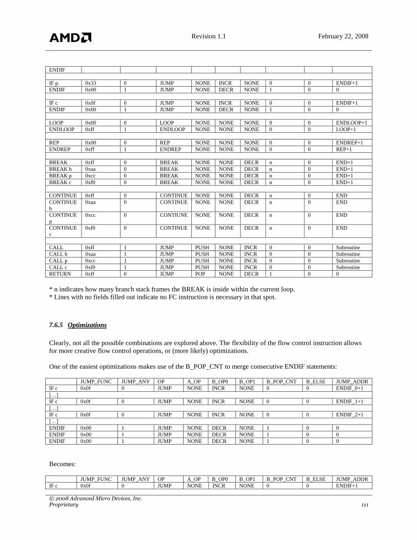
Revision 1.1 February 22, 2008
© 2008 Advanced Micro Devices, Inc. Proprietary 111
ENDIF
IF p 0x33 0 JUMP NONE INCR NONE 0 0 ENDIF+1
ENDIF 0x00 1 JUMP NONE DECR NONE 1 0 0
IF c 0x0f 0 JUMP NONE INCR NONE 0 0 ENDIF+1
ENDIF 0x00 1 JUMP NONE DECR NONE 1 0 0
LOOP 0x00 0 LOOP NONE NONE NONE 0 0 ENDLOOP+1
ENDLOOP 0xff 1 ENDLOOP NONE NONE NONE 0 0 LOOP+1
REP 0x00 0 REP NONE NONE NONE 0 0 ENDREP+1
ENDREP 0xff 1 ENDREP NONE NONE NONE 0 0 REP+1
BREAK 0xff 0 BREAK NONE NONE DECR n 0 END+1
BREAK b 0xaa 0 BREAK NONE NONE DECR n 0 END+1
BREAK p 0xcc 0 BREAK NONE NONE DECR n 0 END+1
BREAK c 0xf0 0 BREAK NONE NONE DECR n 0 END+1
CONTINUE 0xff 0 CONTINUE NONE NONE DECR n 0 END
CONTINUE
b
0xaa 0 CONTINUE NONE NONE DECR n 0 END
CONTINUE p
0xcc 0 CONTIUNE NONE NONE DECR n 0 END
CONTINUE
c
0xf0 0 CONTINUE NONE NONE DECR n 0 END
CALL 0xff 1 JUMP PUSH NONE INCR 0 0 Subroutine
CALL b 0xaa 1 JUMP PUSH NONE INCR 0 0 Subroutine
CALL p 0xcc 1 JUMP PUSH NONE INCR 0 0 Subroutine
CALL c 0xf0 1 JUMP PUSH NONE INCR 0 0 Subroutine
RETURN 0xff 0 JUMP POP NONE DECR 1 0 0
* n indicates how many branch stack frames the BREAK is inside within the current loop.
* Lines with no fields filled out indicate no FC instruction is necessary in that spot.
7.6.5 Optimizations
Clearly, not all the possible combinations are explored above. The flexibility of the flow control instruction allows
for more creative flow control operations, or (more likely) optimizations.
One of the easiest optimizations makes use of the B_POP_CNT to merge consecutive ENDIF statements:
JUMP_FUNC JUMP_ANY OP A_OP B_OP0 B_OP1 B_POP_CNT B_ELSE JUMP_ADDR
IF c 0x0f 0 JUMP NONE INCR NONE 0 0 ENDIF_0+1
[…]
IF c 0x0f 0 JUMP NONE INCR NONE 0 0 ENDIF_1+1
[…]
IF c 0x0f 0 JUMP NONE INCR NONE 0 0 ENDIF_2+1
[…]
ENDIF 0x00 1 JUMP NONE DECR NONE 1 0 0
ENDIF 0x00 1 JUMP NONE DECR NONE 1 0 0
ENDIF 0x00 1 JUMP NONE DECR NONE 1 0 0
Becomes:
JUMP_FUNC JUMP_ANY OP A_OP B_OP0 B_OP1 B_POP_CNT B_ELSE JUMP_ADDR
IF c 0x0f 0 JUMP NONE INCR NONE 0 0 ENDIF+1

Revision 1.1 February 22, 2008
© 2008 Advanced Micro Devices, Inc. Proprietary 112
[…]
IF c 0x0f 0 JUMP NONE INCR DECR 1 0 ENDIF+1
[…]
IF c 0x0f 0 JUMP NONE INCR DECR 2 0 ENDIF+1
[…]
ENDIF
ENDIF
ENDIF 0x00 1 JUMP NONE DECR NONE 3 0 0
7.6.6 LAST Bit
The LAST bit in the US_CMN_INST instruction word allows shaders to terminate before reaching the address
indicated by US_CODE_SIZE.END_ADDR. The LAST bit can be indicated for any instruction type. Any active
pixel for an instruction of any type (FC, ALU, OUTPUT or TEX) marked "last" will be considered "done" for that
instruction and all future instructions that the shader might execute for that thread. Future instructions may or may
not be executed, according to the hardware implementation.
In the R5xx hardware implementation, when all pixels are "done" in a thread and we hit an OUTPUT instruction
that is marked as "last" (and has a texture semaphore wait! -- this is required), we will stop the thread, even if this
isn't the instruction specified by END_ADDR. Also, pixels that are "done" behave the same as pixels considered
"inactive" when encountering flow control instructions, meaning that code that would have been skipped over if all
pixels were "inactive" would also be skipped over if the only pixels marked as "active" were also marked as "done."
7.7 Floating Point Issues
The US is designed to be compliant with the Shader Model 3, which does not officially support IEEE special values
(denormal, infinity, NaN), and allows for leniency in various corner cases.
The US strives to provide a more complete IEEE floating point implementation. US supports the IEEE 32-bit
floating point format, with 23 bits mantissa, 8 bits biased exponent (bias 127), and 1 bit sign. The US also supports
the special IEEE values (denormal, infinity, NaN), but there are some important caveats in the implementation
which are noted below. There is no distinction between an sNaN and a qNaN.
7.7.1 Deviations from IEEE
The most pervasive caveat is that denormals are flushed to an appropriately signed zero throughout US. There is no
gradual underflow, and identities are not preserved for denormal values. This will be apparent in comparison
operations where a denormal is treated as equivalent to zero.
Also pervasive, the internal rounding mode is not configurable and is not exact to the IEEE standard. It could best
be said that rounding is random; operations in and near US round with differing standards and it is infeasible to
specify a uniform rounding mode at this stage of design. Most ALU operations are accurate to within one bit on
each input; transcendental functions have larger tolerances.
The lack of separable multiply and add instructions has consequences on rounding and sign preservation; when
using MAD to perform only a multiply or addition, keep in mind that the other operation may influence the result
despite apparent identities. For example, the obvious instructions to use for moving a value from one register to
another both utilize MAD, either with the additive identity "0 * 0 + r1", or a combination of additive and
multiplicative identities, "r0 * 1 + 0". Neither these instructions will correctly copy -0.0, because the adder cannot
generate -0.0 except with two negative inputs. In this case, a more accurate move instruction would be "-0 * 0 + r1".
(the ideal MOV instruction is described below).
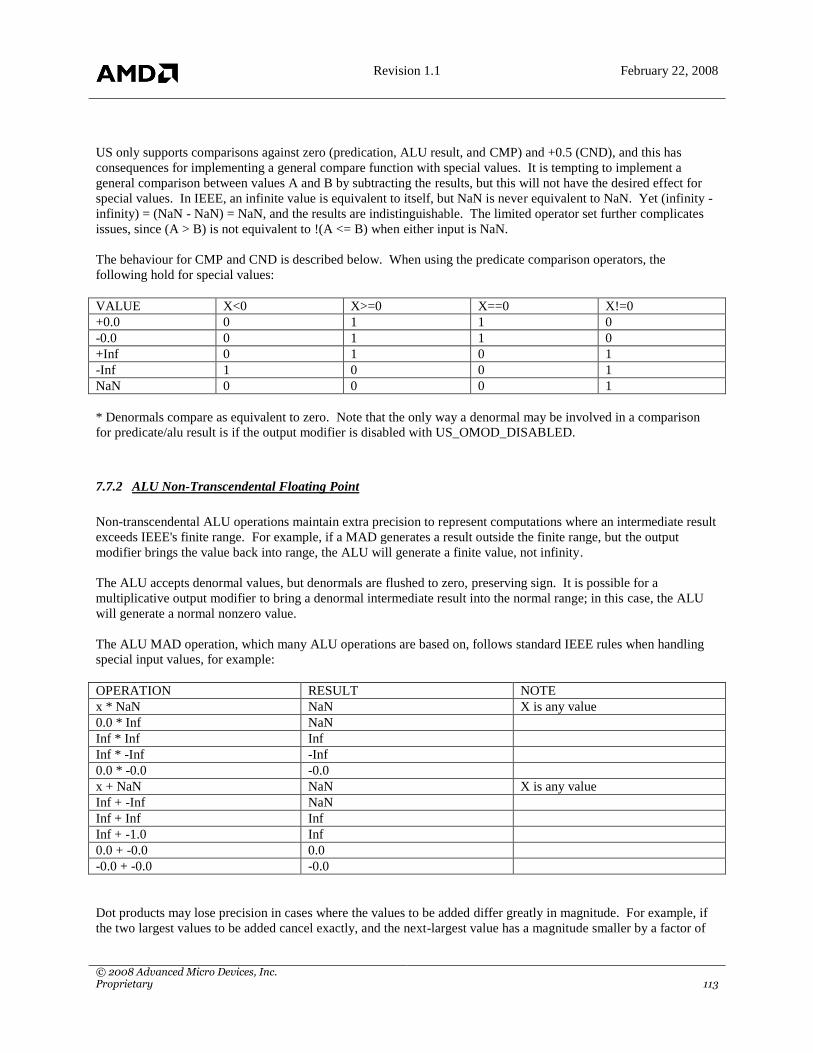
Revision 1.1 February 22, 2008
© 2008 Advanced Micro Devices, Inc. Proprietary 113
US only supports comparisons against zero (predication, ALU result, and CMP) and +0.5 (CND), and this has
consequences for implementing a general compare function with special values. It is tempting to implement a
general comparison between values A and B by subtracting the results, but this will not have the desired effect for
special values. In IEEE, an infinite value is equivalent to itself, but NaN is never equivalent to NaN. Yet (infinity -
infinity) = (NaN - NaN) = NaN, and the results are indistinguishable. The limited operator set further complicates
issues, since (A > B) is not equivalent to !(A <= B) when either input is NaN.
The behaviour for CMP and CND is described below. When using the predicate comparison operators, the
following hold for special values:
VALUE X<0 X>=0 X==0 X!=0
+0.0 0 1 1 0
-0.0 0 1 1 0
+Inf 0 1 0 1
-Inf 1 0 0 1
NaN 0 0 0 1
* Denormals compare as equivalent to zero. Note that the only way a denormal may be involved in a comparison
for predicate/alu result is if the output modifier is disabled with US_OMOD_DISABLED.
7.7.2 ALU Non-Transcendental Floating Point
Non-transcendental ALU operations maintain extra precision to represent computations where an intermediate result
exceeds IEEE's finite range. For example, if a MAD generates a result outside the finite range, but the output
modifier brings the value back into range, the ALU will generate a finite value, not infinity.
The ALU accepts denormal values, but denormals are flushed to zero, preserving sign. It is possible for a
multiplicative output modifier to bring a denormal intermediate result into the normal range; in this case, the ALU
will generate a normal nonzero value.
The ALU MAD operation, which many ALU operations are based on, follows standard IEEE rules when handling
special input values, for example:
OPERATION RESULT NOTE
x * NaN NaN X is any value
0.0 * Inf NaN
Inf * Inf Inf
Inf * -Inf -Inf
0.0 * -0.0 -0.0
x + NaN NaN X is any value
Inf + -Inf NaN
Inf + Inf Inf
Inf + -1.0 Inf
0.0 + -0.0 0.0
-0.0 + -0.0 -0.0
Dot products may lose precision in cases where the values to be added differ greatly in magnitude. For example, if
the two largest values to be added cancel exactly, and the next-largest value has a magnitude smaller by a factor of

Revision 1.1 February 22, 2008
© 2008 Advanced Micro Devices, Inc. Proprietary 114
2^25 or more, US will emit +0.0 rather than the sum of the two remaining components. IEEE is silent on the
behavior of such fused operations, and it seems unlikely that this condition will manifest very often.
MIN and MAX operations return the second argument if either input is NaN (this is consistent with IEEE and SM3
specifications); infinite values compare as usual. If both inputs are +-0.0, MIN and MAX will return the second
input (consistent with IEEE and the SM3 spec) – as a result, MIN(+0, -0) == -0, and MIN(-0, +0) == +0.
CND and CMP operations return the second argument if either input is NaN; infinite values compare as usual. As
with the predicate compare operators, +0.0 and -0.0 are both "equal" to 0.
MIN, MAX, CND, and CMP are guaranteed to return one of their first two arguments. If you use
US_OMOD_DISABLED as well, then you will get a bit-exact representation of one of the first two arguments.
ALU operations usually enable the output modifier, which in turn standardizes NaN values and flushes denormal
results to zero. A MOV instruction which preserves the source bits may be implemented by setting
US_OMOD_DISABLED for the instruction and using the MAX(src, src) instruction. The output modifier cannot be
disabled for a saturated MOV (MOV with clamping enabled).
7.7.3 ALU Transcendental Floating Point
In US, transcendental operations are EX2, LN2, RCP, RSQ, SIN, and COS (mathematically speaking, one of these
functions does not belong). Transcendentals do not maintain extra internal precision; as a result, if the result of the
transcendental operation exceeds the IEEE finite range, the ALU will generate infinity even if the output modifier
would bring the result back into range. Similarly if the result is denormal, the ALU will generate a pure zero
(preserving sign) even if the output modifier would bring the result back into the normal range.
Special values are computed as shown in the following table:
INPUT EX2 LN2 RCP RSQ SIN COS
+0.0 +1.0 -Inf +Inf +Inf +0.0 +1.0
-0.0 +1.0 -Inf -Inf +Inf * -0.0 +1.0
+Inf +Inf +Inf +0.0 +0.0 NaN NaN
-Inf +0.0 NaN -0.0 NaN NaN NaN
NaN NaN NaN NaN NaN NaN NaN
* For RSQ, recall that the square root occurs first. IEEE specifies sqrt(-0.0) -> -0.0; the US deviates from this,
however this does not affect SM3 compliance since RSQ is always used with the absolute value input modifier for
SM3 shaders.
7.7.4 Texture Floating Point
Projected and cubemapped texture coordinates are processed in the US block before being sent to the texture unit.
The texture unit does not accept NaN, so NaN coordinates are converted to +infinity before being sent to the texture
unit. As with the ALU, denormal inputs and denormal results are converted to pure zero, preserving sign.
The multiplier used for projection and cubemapping does not follow IEEE rules when handling special values. This
will become apparent only when you attempt to project or cubemap a coordinate that contains an infinite or NaN
component.

Revision 1.1 February 22, 2008
© 2008 Advanced Micro Devices, Inc. Proprietary 115
You should use caution when generating very large values for use as coordinates in a texture lookup. These values
may generate infinite values when scaled by the texture dimensions, projected, or cubemapped.
7.7.5 Legacy multiply behaviour
By default multiplication by zero is IEEE-compliant for any ALU instruction. To support legacy (SM1.x) shaders
which did not have an IEEE-compliant multiplier, set
US_CONFIG.ZERO_TIMES_ANYTHING_EQUALS_ZERO. Setting this bit will cause the multiplier used by
MAD, dot products, MDH and MDV to treat "+-0 * x == +0" for all values x. Note that IEEE deviates from this
behaviour when x is infinity or NaN. Modern shaders should not set this bit.
7.8 Writing to US Registers
The US configuration, integer constant, and boolean constant registers can be written to directly. However due to
addressing limitations elsewhere in the pipe, the US instruction and ALU constant registers cannot be written
directly; they must be programmed via a vector mechanism provided in the GA block. You write to the vector in
two parts; first, you program the write destination in GA_US_VECTOR_INDEX, then you write data to
GA_US_VECTOR_DATA until you have set all the values of interest.
7.8.1 Writing instructions
To write one or more shader instructions, set GA_US_VECTOR_INDEX.TYPE to GA_US_VECTOR_INST and
GA_US_VECTOR_INDEX.INDEX to the address of the first shader instruction you want to write (from 0 to 511).
Then write each instruction register to GA_US_VECTOR_DATA (usually, a total of 6 writes per instruction), in the
following order:
ALU/OUTPUT TEX FC
0: US_CMN_INST US_CMN_INST US_CMN_INST
1: US_ALU_RGB_ADDR US_TEX_INST 0
2: US_ALU_ALPHA_ADDR US_TEX_ADDR US_FC_INST
3: US_ALU_RGB_INST US_TEX_ADDR_DXDY US_FC_ADDR
4: US_ALU_ALPHA_INST 0 0
5: US_ALU_RGBA_INST 0 0
A few notes:
If you are writing an FC or TEX instruction, you may need to pad the vector with zeros; note that a zero
dword must be written in the middle of the FC instruction.
You can write to multiple instructions without updating the index. After you write 6 values to
GA_US_VECTOR_DATA, the GA will automatically increment the instruction index. The index wraps at
512.
If the last instruction you write to is a TEX or FC instruction, you do not need to write the last two zero
dwords that are used for padding.
Similarly, if you do not need to update all instruction registers for the last instruction you write, you do not
need to write the registers that follow it.
You should always write to GA_US_VECTOR_INDEX before writing a sequence of instructions, to
ensure the GA is setup appropriately.

Revision 1.1 February 22, 2008
© 2008 Advanced Micro Devices, Inc. Proprietary 116
7.8.2 Writing ALU constants
To write one or more ALU constants, set GA_US_VECTOR_INDEX.TYPE to GA_US_VECTOR_CONST and
GA_US_VECTOR_INDEX.INDEX to the address of the first constant you want to write (from 0 to 255). Then
write each constant register to GA_US_VECTOR_DATA (usually, a total of 4 writes per constant), in the following
order:
0: US_ALU_CONST_R
1: US_ALU_CONST_G
2: US_ALU_CONST_B
3: US_ALU_CONST_A
A few notes:
You can write to multiple constants without updating the index. After you write 4 values to
GA_US_VECTOR_DATA, the GA will automatically increment the constant index.
If you do not need to update all components of the last constant you write, you do not need to write the
components that follow it.
You should always write to GA_US_VECTOR_INDEX before writing a sequence of constants, to ensure
the GA is setup appropriately.

Revision 1.1 February 22, 2008
© 2008 Advanced Micro Devices, Inc. Proprietary 117
8. HiZ
8.1 Introduction
The R5xx HiZ (Hierarchical Z) unit performs a coarse z occlusion test on a tile of pixels to generate a mask
indicating whether a set of quads within the tile is potentially visible. The Scan Converter (SC) block uses this mask
to determine which quads will be passed on to the Rasterizer (RS) and which will be pruned. In this manner, HiZ
provides an early-out mechanism for dropping quads.
This section presents an overview of the operation of the HiZ unit and a guide on how to program it.
8.2 Enabling HiZ
HiZ operation must be enabled in both the SC and ZB. It is enabled or disabled in the SC by setting the HZ_EN field
in the SC_HYPERZ_EN field to 1 or 0. Similarly, it is enabled or disabled in the ZB by setting the HIZ_ENABLE
field in the ZB_BW_CNTL register to 1 or 0.
8.3 Configuring HiZ
The following registers must be set to configure the HiZ unit for operation.
The ZB_HIZ_PITCH register specifies the pitch of the HiZ buffer in HiZ RAM. The host writes the pitch in pixels.
The register interprets bits [13:4] as the 16 pixel-aligned HIZ_PITCH field. This field is used as pitch_mux in
formula 1 in section 2.2, which calculates the DWORD address in HiZ RAM where z floor updates are written
during z cache line evictions.
The ZB_HIZ_OFFSET register specifies a base offset into HiZ RAM. Bits [16:2] of this register are the DWORD-
aligned HIZ_OFFSET field.
The HZ_MAX field in the SC_HYPERZ_EN register specifies whether the minimum or maximum z in the 8x8 tile
is interpreted as the closest z whose floor is sent to the HiZ unit. The definition of which is the closest depends on
the sense of the z function. For instance, if the z function is LESS, the minimum value is the closest. The
programmer should set this field according to the z comparison function that is set in the ZFUNC field of the
ZB_ZSTENCILCNTL register. Setting SC_HYPERZ_EN.HZ_MAX to 0 sends the floor of the minimum, and
setting it to 1 sends the floor of the maximum.
The HIZ_MIN field of the ZB_BW_CNTL register specifies whether the HiZ unit updates the HiZ RAM with the
floor of the minimum or maximum z value during z cache line evictions. As with the SC_HYPERZ_EN.HZ_MAX
field, this field is also dependant on the z function set in the ZB_ZSTENCILCNTL. Setting HIZ_MIN to 0 updates
HiZ RAM with the floor of the maximum z, and 1 updates with the floor of the minimum.
The following table shows how the SC_HYPERZ_EN.HZ_MAX and ZB_BW_CNTL. HIZ_MIN fields should be
set according to ZFUNC. It also shows what the HiZ RAM should be initially cleared to, and what action the HiZ

Revision 1.1 February 22, 2008
© 2008 Advanced Micro Devices, Inc. Proprietary 118
comparison takes. The „Z_MINMAX‟ column corresponds to the SC_HYPERZ_EN.HZ_MAX setting, and the „ZB
write to HiZ(X, Y)‟ corresponds to the ZB_BW_CNTL. HIZ_MIN setting.
ZFUNC HiZ Clear
Value
Z_MINMAX HZ 2nd
Level Z Function ZB write to HIZ(X,Y)
0 - Never Don‟t Care Min(Z0, Z1,
Z2)
Prune the Block Don‟t care
1 - Less Floor(Z_Clear) Min(Z0, Z1,
Z2)
If (floor(Z_MINMAX) >
HiZ(X,Y))
Prune the Block
Else
Pass the Block
Floor(Maximum(Z))
2 - Less or Equal Floor(Z_Clear) Min(Z0, Z1,
Z2)
If (floor(Z_MINMAX) >
HiZ(X,Y))
Prune the Block
Else
Pass the Block
Floor(Maximum(Z))
3 - Equal Don‟t Care Min(Z0, Z1,
Z2)
Pass the Block Don‟t care
4 - Greater or
Equal
Floor(Z_Clear) Max(Z0, Z1,
Z2)
If (floor(Z_MINMAX) <
HiZ(X,Y))
Prune the Block
Else
Pass the Block
Floor(Minimum(Z))
5 - Greater Than Floor(Z_Clear) Max(Z0, Z1,
Z2)
If (floor(Z_MINMAX) <
HiZ(X,Y))
Prune the Block
Else
Pass the Block
Floor(Minimum(Z))

Revision 1.1 February 22, 2008
© 2008 Advanced Micro Devices, Inc. Proprietary 119
6 - Not Equal Don‟t Care Max(Z0, Z1,
Z2)
Pass the Block Don‟t Care
7 - Always Don‟t Care Max(Z0, Z1,
Z2)
Pass the Block Don‟t Care
8.4 HiZ Clear with PM4 Packet
The most efficient manner for a driver to clear HiZ RAM is to use the 3D_CLEAR_HIZ Type-3 PM4 packet. The
3D_CLEAR_HIZ packet is described below.
3D_CLEAR_HIZ
Functionality
Clear HIZ RAM.
Format
Ordinal Field Name Description
1 [ HEADER ] Header of the packet
2 START Start
3 COUNT[13:0] Count[13:0] – Maximum is 0x3FFF.
4 CLEAR_VALUE The value to write into the HIZ RAM.
8.5 Example: Putting it All Together
Here is a simple example that demonstrates typical steps in setting up the HiZ unit:
// enable z buffering
regwrite (ZB_CNTL, Z_ENABLE, 1);
// set the ZFUNC to LESS
regwrite (ZB_ZSTENCILCNTL, ZFUNC, 1); // 1 = LESS
// enable HiZ in the SC
regwrite (SC_HYPERZ_EN, HZ_EN, 1);
// enable HiZ in the ZB
regwrite (ZB_BW_CNTL, HZ_EN, 1);
// set HZ_MAX in SC_HYPERZ_EN to MIN for ZFUNC=LESS
regwrite (SC_HYPERZ_EN, HZ_MAX, 0);
// set HIZ_MIN in ZB_BW_CNTL to MAX for ZFUNC=LESS
regwrite (ZB_BW_CNTL, HZ_MIN, 0);
// set HIZ_OFFSET to 0
regwrite (ZB_HIZ_OFFSET, HIZ_OFFSET, 0);
// set HIZ_PITCH to 1024
regwrite (ZB_HIZ_PITCH, HIZ_PITCH, 1024 >> 4);
// initialize the HiZ RAM to a clear value of 0xff
// for all the bytes in a 1024x768 area:
// set initial write index. It will auto-increment
// after each write to ZB_HIZ_DWORD
regwrite (ZB_HIZ_WINDEX, HIZ_WINDEX, 0);

Revision 1.1 February 22, 2008
© 2008 Advanced Micro Devices, Inc. Proprietary 120
// write floors for one 8x8 tile with each DWORD.
// this example assumes a dual-pipeline configuration.
// since half the screen is owned by the second pipeline,
// and host writes are broadcast to both pipeline RAMS
// at the same address, we write the clear DWORD for
// half of 1024>>3. In a single-pipeline configuration,
// we would write the clear DWORD for 1024>>3.
for (int y = 0; y < (768 >> 3); y++)
{
for (int x = 0; x < ((1024 >> 3)>1); x++)
{
regwrite (ZB_HIZ_DWORD, HIZ_DATA, 0xffffffffL);
}
}
// read back a DWORD in pipeline 1 at address 0
regwrite (SU_REG_DEST, SELECT, 1);
regwrite (ZB_HIZ_RINDEX, 0);
DWORD dwGetHiZValue = regread (ZB_HIZ_DWORD);
8.6 State Changes That Invalidate HiZ
This section describes the conditions that invalidate HiZ RAM and those that have no effect.
Disabling Z testing or disabling Z writes does not invalidate HiZ RAM, so no special action is required in these
cases. Because both of these states result in no new z data being written to the z buffer, there are no z cache
evictions that update the contents of HiZ RAM. Therefore, HiZ RAM is preserved and can continue to be used after
Z buffering or Z writes are re-enabled.
Certain ZFUNC transitions can invalidate the contents of HiZ RAM. As a general rule, the safest approach when
ZFUNC is changed is to disable HiZ testing until the contents of HiZ RAM are reset, e.g. until the start of the next
frame where HiZ RAM is re-initialised. Having said that, there are transitions where either HiZ does not need to be
disabled, or it may be re-enabled before the end of the frame:
1) HiZ does not need to be turned off when transitioning back and forth between LESS and LESSEQUAL.
HiZ must be disabled when transitioning from either LESS or LESSEQUAL to EQUAL, but may be re-
enabled when transitioning back from EQUAL to LESS or LESSEQUAL.
2) HiZ does not need to be turned off when transitioning back and forth between GREATER and
GREATEREQUAL. HiZ must be disabled when transitioning from either GREATER or
GREATEREQUAL to EQUAL, but may be re-enabled when transitioning back from EQUAL to
GREATER or GREATEREQUAL.
All other transitions invalidate the contents of HiZ RAM with respect to the new sense of the z comparison.
Revision 1.1 February 22, 2008
© 2008 Advanced Micro Devices, Inc. Proprietary 121
9. Driver notes
9.1 R5xx Changes
9.1.1 PS3.0
R520 TX supports pixel shader model 3.0. Support for 32-bit IEEE input coordinates from the shader and 32-bit
IEEE output colors to the shader. Support for per pixel (or per quad) TEXLDB, TEXLDL, and TEXLDD
instructions.
9.1.2 Filter4
R520 can support limited Filter4 filtering. The kernel is 4x4 symmetric and separable with 16 phases. The kernel
weight precision is S,1.9. There is one global kernel shared by all textures. The kernel is loaded using the global
TX_FILTER4 register. Filter4 can be enabled per texture using the MAG and MIN filter registers. Only one of four
8-bit components can have Filter4 applied at a time. That component is selected using FORMAT2.SEL_FILTER4.
9.1.3 Maximum Image Extents
R520 supports up to 4K texels in width, height, or depth.
9.1.4 Trilinear Interpolation Precision
R520 supports 6-bits of trilinear precision. R420 supported 5-bits.
9.1.5 Image Formats
New image formats over R420 : ATI1N, 10, 10_10, 10_10_10_10, 1, 1_REVERSED
9.1.6 Border Color
Added border color support for FAT formats, specifically 16_16_16_16, 16f_16f_16f_16f, 32f_32f,
32f_32f_32f_32f. Border color is now supported for all image formats.
9.1.7 Non-Square mipmaps with border color
Added mode register FILTER1.BORDER_FIX which when asserted will stop right shifting the texture coordinate
once the image size has been right shifted to one. BORDER_FIX only needs to be asserted when the clamp mode is
a border mode and mipmapping is enabled and the mipmap is non-square. However it should be safe to assert
BORDER_FIX anytime.
9.1.8 POW2FIX2FLT
Added mode register FORMAT2.POW2FIX2FLT which when asserted the TX will divide by pow2 instead of
pow2-1 when doing fix2float conversion of the filtered texture color.
9.1.9 GA_IDLE
R520 has a new status register called GA_IDLE which can be used to get information about back-end hangs. To
read this register, the following procedure may be used:
Read RBBM_STATUS to make sure the HW is hung. If GA bit is busy, this may indicate a
back-end hang.
Write 0x32005 to the RBBM_SOFTRESET register. This is to reset GA, CP and VAP.

Revision 1.1 February 22, 2008
© 2008 Advanced Micro Devices, Inc. Proprietary 122
Read RBBM_SOFTRESET to make sure the write went through.
Write 0 to RBBM_SOFTRESET. This is necessary to get VAP to go idle.
RBBM_STATUS should now show that VAP and CP are idle but GA still busy. If GA is not busy,
then GA_IDLE should be readable at this point.
If GA was still hung, write 0x200 to GA_SOFTRESET
Now GA_IDLE can be read. See the register spec for details on what each bit means. Note that a “1”
indicates an idle unit.
9.1.10 HDP surface0 upper bound 64 byte alignment requirement
HDP surface 0 upper bound needs at least 64 byte alignment. This applies only to surface 0 and not to surface 1 to
7, which can be programmed as specified (32 byte aligned).
9.1.11 New Soft resets for CP
CP now has total of 3 soft resets:
CP_SOFT_RESET => as before (for backward compatibility).
CP_SOFT_RESET_NO_DMA => soft reset CP except DMA engine.
CP_SOFT_RESET_DMA => soft reset only DMA engine of CP.
9.1.12 CP STOP_CONTEXT
Once SC/CB informs CP to stop_context, CP will not fetch/process any further read requests from command
buffers.
9.1.13 Updated CP Scratch compare logic
Scratch register interrupt functions as follows:
(a) Driver programs two 32bit registers with timestamp for comparisons with a pair of scratch registers. We can call
this as DRV_REGS
(b) Driver programs PM4 stream with writes to two consecutive scratch registers (paired as 0-1,2-3,4-5,6-7) to be
compared with DRV_REGS.
(c) In due course of time PM4 pkt would get executed , this address/data would sit in the input fifo of CP , ready to
program both the scratch registers.
(d) As soon as CB (color buffer) sends two sets of RESYNC pulses (4 of them from each pipe with mask), CP
allows the FIFO contents to get transferred to scratch registers for further action. (RBBM transactions are stalled at
this time)
(e) SCR_REGS data gets compared with DRV_REGS data for preprogrammed condition of either "equality" or
"non-equality" or "greater than" or "less than " or "greater than or equal" or "less than or equal".
Revision 1.1 February 22, 2008
© 2008 Advanced Micro Devices, Inc. Proprietary 123
(f) If the condition is satisfied then an interrupt is generated informing driver/system to wake-up and proceed for the
next command.
(g) The scratch register data gets written to system memory (if umask is set) at premapped address to be read back
by the system/driver.
9.1.14 Host requests (GFX, ISYNC_CNTL, RBBM_GUICNTL, WAIT_UNTIL)
Pre-R5xx, requests made within the aperture range 0x1400 - 0x1EFF and 0x2000 – 0xFFFF were queued. From
R5xx, onwards these requests will not be queued. ISYNC_CNTL, RBBM_GUICNTL and WAIT_UNTIL can be
programmed only for queued requests. As none of the host (PIO) requests are queued, host cannot program above
three registers through PIO.
9.1.15 Double Z
RV530 has two Z pipes, but a single raster pipe. In the past, SU_REGDEST was used to select which raster pipe
you want to select. On RV530, you use FG_ZBREG_DEST. Because the pipe selection happens in the FG, you
must be in Z bottom mode. This mainly applies to occlusion queries where you want to get Z pass data from each
Z unit.
9.1.16 FP16 AA support
R5xx-family chips support FP16 AA. However, there is an issue with the blend optimizations while FP16 AA is
enabled. Because of this, RB3D_BLENDCNTL.DISCARD_SRC_PIXELS must be set to
CB_DISCARD_SRC_DISABLE while FP 16 AA is enabled.
9.1.17 FP16 Blending
FP16 (64bit pixel) blending is added in R5xx parts. FP16 Blend bandwidth is half the rate of 32 bit pixels; i.e. 8
pixels/clk in a 16 pipe system. FP16 blending uses the new 64 bit clear color register and constant color registers.
Setting the FP16 blend equation to multiply by 1.0 is subtly different from disabling blending. A negative zero
(0x8000) will be converted to zero (0x0000) if it is blended but 0x8000 will be drawn if blending is disabled. The
driver should distinguish between FP16 and 16 bit integer formats and never enable blending for 16 bit integer
formats. The CB FP16 implementation supports denorms but does not support NaNs and Infs. Only a 4 component
(ARGB16161616) format is supported. There are no I16 or IA1616 formats.
9.2 Interface Notes
9.2.1 Raster Reset
The proper sequence for a full raster reset is the following:
Perform a RBBM reset with the GA RBBM client flag set
Perform a register write to the GA_SOFT_RESET register, with a value of 0x200 or higher
In the above sequence, the first item causes the GA to delete all pending register reads & writes and resets the
RBBM interface. If the GA status is idle, then the RBBM reset is not required. After this reset, the GA is ready to
accept register read and write commands. However, the 3D pipe could be in a hung state, which would prevent it

Revision 1.1 February 22, 2008
© 2008 Advanced Micro Devices, Inc. Proprietary 124
from accepting 3D commands or register commands.
The second operations (GA_SOFT_RESET) causes a soft reset of the 3D pipe. This reset causes a loss of all state in
the 3D, except in the GA & SU blocks. Shadow register values are not reset. The 3D pipe should then switch to the
idle state after the reset. It will take 0x200+ cycles for the idle state to be re-asserted (should be less than 0x200 +
64). The value of 0x200 is a suggestion, which should be enough to reset all the pipelines. A larger value can be
used (up to 16b), but should not offer any benefit.
9.2.2 Non-textured, non-colored primitives
The R300 always does at least one 2D texture and one color per primitive. The RS_COUNT has a baseline value of
1, which indicates up to 1 color and 1 texture are to be rasterized. The other registers used to specify the colors and
textures are the VAP_RASTER_VTX_FMT_0 and RASTER_VTX_FMT_1 registers. These registers can be set to
have no color and no texture. So if one wants to specify a non-textured and non-color primitive, one should set the
RASTER_VTX_FMT registers to no color and no texture, and set the RS_COUNT to 0. The raster will still
rasterize the extra colors and textures, but the rasterized values will be wrong. The shader code should then be set to
ignore the texture coordinates and colors and to setup a constant color, or the CB could be disabled so no color
writes occur (to setup the ZB, for example).
9.2.3 Flushing primitives out of the SC
All 3D operations need to be terminated with a register write to the SC, US or some down stream register. Unless
this is done, the SC/RS will never assert idle (which will be reflected as GA_BUSY). The final polygon rendered
should still drain out of the pipe.
9.3 Register Notes
9.3.1 Update to register reads
R520 and follow-on chips now support simultaneous G3D register reads and writes. Coherency of reads and writes
is not guaranteed (reads can occur before writes). However, switching from write/cmd mode to read mode (PIO
through RBBM) does not require idling the G3D pipe anymore. However, this mode is not enabled by default. The
following fields have been added to the GA_ENHANCE register:
REG_READWRITE 2:2
REG_NOSTALL 3:3
When the REG_READWRITE field is set, this enables the GA to support simultaneous register reads and writes.
However, simply enabling this mode allows the GA to receive both read and write commands (and to deal with
both), but it still tells the GA to wait for register return before continuing. Consequently, the GA will cause a stall
bubble, of (n) cycles to be injected, where (n) is the latency for register read back. If the register is shadowed, that
value is very small (A few cycles). If not, then it can be hundreds of cycles
When REG_NOSTALL field is set, this enables GA to support mixing the G3D pipe with reads and other activity;
in this mode, the register read is simply part of the pipeline data. This mode would allow for no performance hit at
all, when doing register reads, since the GA will not cause a stall bubble (it will not wait for the register data to
return). It does not permit the GA to have multiple outstanding read requests, but it allows for minimal performance
impact.
9.3.2 Registers that cause stalls

Revision 1.1 February 22, 2008
© 2008 Advanced Micro Devices, Inc. Proprietary 125
9.3.2.1 ZB Registers
Unpipelined registers
Writes to these registers causes a stall in the pipe. The stall is on as long as there are any quads in the ZB block.
Once the ZB block is empty the register is updated and the stall is removed. If multiple unpipelined registers are
updated with no quads in the middle, then the first one will cause a stall to drain the ZB, but the following
unpipelined writes will go at full speed…
ZB_FORMAT
ZB_ZCACHE_CTLSTAT
ZB_BW_CNTL
ZB_DEPTHOFFSET
ZB_DEPTHPITCH
ZB_DEPTHCLEARVALUE
ZB_HIZ_OFFSET
ZB_ZPASS_DATA
ZB_ZPASS_ADDR
ZB_DEPTHXY_OFFSET
Pipelined Registers
ZB_CNTL
ZB_ZSTENCILCNTL
ZB_STENCILREFMASK
ZB_HIZ_DWORD
Special register ZTOP
Whenever ZTOP register is switched from 1 to 0 or 0 to 1 a stall occurs at the SC stage of the pipe and it goes away
when all the quads between the SC and CB are drained from the pipe. Then the Zbuffer is moved in the pipe-lined.
Writing to Ztop a value that it currently holds (0 to 0 or 1 to 1) has no performance penalty.
9.3.2.2 CB Registers
Unpipelined registers
Writes to unpipelined registers cause the CB to stall until all previous quads, pipelined registers, and partially
pipelined registers have finished processing. Once an unpipelined register has been written, a write to another
unpipelined register will not cause more stalls as long as there are no intervening quads, pipelined registers, or
partially pipelined registers. The unpipelined CB registers are the following:
RB3D_CCTL
RB3D_COLOR_CLEAR_VALUE
RB3D_COLOROFFSET(0, 1, 2, 3)
RB3D_COLORPITCH(0, 1, 2, 3)
RB3D_DSTCACHE_CTLSTAT
RB3D_AARESOLVE_OFFSET
RB3D_AARESOLVE_PITCH
RB3D_AARESOLVE_CTL
GB_TILE_CONFIG
GB_AA_CONFIG
Partially pipelined registers
Partially pipelined registers are pipelined everywhere in the CB except in one module. That module must stall until
all the quads that it is currently processing have finished. The number of stall cycles should not exceed about 15
cycles. The partially pipelined CB registers are the following:

Revision 1.1 February 22, 2008
© 2008 Advanced Micro Devices, Inc. Proprietary 126
RB3D_ROPCNTL
RB3D_CLRCMP_FLIPE
RB3D_CLRCMP_CLR
RB3D_CLRCMP_MSK
Pipelined registers
These registers are fully pipelined and may be freely intermixed with quads without causing stalls. The pipelined
registers are the following:
RB3D_BLENDCNTL
RB3D_ABLENDCNTL
RB3D_COLOR_CHANNEL_MASK
RB3D_CONSTANT_COLOR
RB3D_DITHER_CTL
CB register ordering
Because unpipelined registers can stall on preceding pipelined or partially pipelined registers, it is recommended
that all unpipelined registers are written first. Pipelined and partially pipelined registers may be freely intermixed
without penalty.
9.3.2.3 TX Registers
Global registers
Global registers are registers that affect all texture stages. On a write to any global texture register, the US will wait
for the TX to flush completely before passing the register to the TX. This could take on the order of a couple
hundred clocks worst case. Obviously writes to these registers should be minimized. There are two global registers
that cause the TX to flush : TX_INVALTAGS and TX_PERF.
Stage registers
Stage registers are registers that only affect 1 of the 16 possible texture stages. On a write to a Stage register, the US
will wait until that texture stage is inactive in the TX pipe, and only then will it pass the register to the TX. It is
therefore important to rotate through the 16 sets of registers to avoid a register write to a stage that is still being
processed in the TX. Otherwise unnecessary stalls will occur.
9.3.3 Registers that affect performance
9.3.3.1 US_W_FMT
When the W value is not being used (FG_DEPTH_SRC does not select discrete W), then this register should be set
to specify that the source is the US and the format is always 0. Specifying that W comes from the rasterizer causes
stalls inside the US.
9.3.4 Other Registers
9.3.4.1 GB_TILE_CONFIG
The GB_TILE_CONFIG contains multiple raster pipe control fields. Some of these need a soft reset afterwards to
apply the change. All of them require the pipe to be idle before performing the change. As well, in the R5xx, this
register is simply shadowed in the shadow RAM, except for the PIPE_COUNT field, which always indicates the
internal value of this field. This might or might not match the written value, depending on bad_pipes and max_pipes.
All fields after Hard reset will show the default values shown below. The fields all hard reset to the default values.

Revision 1.1 February 22, 2008
© 2008 Advanced Micro Devices, Inc. Proprietary 127
Soft reset (GA_SOFT_RESET) does not affect this register.
Here are the fields, with the default values, the reset status and a slight comment:
Fields Possible values Defaults Reset Comments
Enable [0:0] 0: Disable tiling
1: Enable tiling
Enabled (1) If changed, soft
reset should be
applied
The default value of
(1) should never be
changed
Pipe_count [3:1] 0: RV350
3: R300
6: R420 (3 pipes)
7: R420 (4 pipes)
Depends on fuses If changed, soft
reset should be
applied
Should be
programmed with 4P
(7), 3P (6), 2P (3) or
1P (0).
Tile_size [5:4] 0: 8x8 pixels
1: 16x16 pixels
2: 32x32 pixels
1 : 16x16 No reset required R5xx supports 16x16
or 32x32 only.
32x32 should be
used, in 3p or 4p
cases, as performance
testing determines
Super_size [8:6] 0: 1x1 tile
1: two 1x1 A,B tiles
2: one 2x2 tile
3: two 2x2 A,B tiles
0: 1x1 tile Only 1x1 mode
guaranteed – Feature
only used in multi-
chip boards
Only support super
tiling with 1, 2 or 4
pipes (not in 3P
config)
Super_X, Super_Y,
Super_Tile [15:9]
7b ID identifies
unique location of
chip in multi-chip
board
0 No reset required When in single chip,
value should be 0.
Subpixel [16:16] 0: 1/12 subpixel
1: 1/16 subpixel
0: 1/12 Can be changed
whenever pipe is
idle without Reset
Selects the 1/12 or
1/16 subpixel mode
Quads_per_ras
[18:17]
0: 4 quads
1: 8 quads
2: 16 quads
3: 32 quads
0: 4 quads No reset required Reserved for R350 –
Leave at 0 for R300,
RV350
Bb_scan [19:19] 0: Use intercept scan
conv.
1: Use bounding box
scan conv.
0: Intercept No reset required Intercept method is
new and higher
performance.
Bounding box is
traditional & slower,
but “guaranteed” to
work. Should only be
changed if raster
issues come up.
Alt_scan_en[20:20] 0: Do Z type scan
conversion
1: Do S type scan
conversion
0: Z type Can be changed
when pipe idle.
RV350 and R420
support S scan
conversion, which
maintains local
coherence from scan
line to scan line,
instead of Z type

Revision 1.1 February 22, 2008
© 2008 Advanced Micro Devices, Inc. Proprietary 128
which “goes back” to
the left on every scan
line
Alt_offset[21:21] 0: Use 1440/1088
offset for SC
1: Use 672/1088
offset for SC
0: 1440/1088 mode Should be
switched when
pipe is idle.
When in mode (1),
allows for a render
target of 4k x 4k,
only for 1/12
subpixel mode. The
X,Y offsets in the GA
are not affected, so
that the viewport
should be loaded with
a value of (672-
1440=-768) to match.
Subprecision [22:22] 0: Uses 4b of sub
pixel precision
1: Uses 8b of sub
pixel precision
0: 4b Should be
changed when
pipe is idle.
Allows for 4 extra
bits of subpixel
precision. All
computations done in
higher precision
when in use. Should
always be enabled.
Alt_tiling [23:23] 0: Use regular tiling
for 3P mode
1: Use alternate
tiling for 3P mode
0: Regular tiling No reset required Empirical testing
needs to be done to
determine which has
higher performance.
Either tiling mode is
possible.
Z_extended[24:24] 0: Use [0,1] Z clamp
range
1: Use [-2,2] Z
range
0: R3xx/R4xx mode Should be
changed when
pipe is idle
Should allow us to
increase guardband.
Per pixel clamping to
[0,1] still occurs in
SC
9.3.4.2 GB_PIPE_SELECT
GB_PIPE_SELECT controls the physical and logical pipe mapping, as well as the total number of active pipes. It
works with GB_TILE_CONFIG to configure the pipelines. It is procedural and not shadowed; if you read the
register back after hard reset, you should get the default values. Changing this register is generally not required, if
the fuses are set correctly (i.e. max_pipes reflects total number of working and desired pipes; bad_pipes indicates
which of the 4 pipes are bad). The MAX_PIPES and BAD_PIPES fields are read-only, and reflect what the SU unit
receives from the fuse unit. The fuse unit can be programmed to alter the max_pipes/bad_pipes, but not contrary to
the actual fuse settings (can never set, through SW, internally max_pipes to higher than the fuse setting).
Fields Possible Values Defaults Reset Comments
PIPE0_ID [1:0] 0, 1, 2, 3 Depends on fuses
– Often 0
Pipe should be
soft reset after
changing
Determines the logical mapping
of physical pipe 0
PIPE1_ID [3:2] 0, 1, 2, 3 Depends on fuses
– Often 1
Pipe should be
soft reset after
changing
Determines the logical mapping
of physical pipe 0
PIPE2_ID [5:4] 0, 1, 2, 3 Depends on fuses
– Often 2
Pipe should be
soft reset after
Determines the logical mapping
of physical pipe 0

Revision 1.1 February 22, 2008
© 2008 Advanced Micro Devices, Inc. Proprietary 129
changing
PIPE3_ID [7:6] 0, 1, 2, 3 Depends on fuses
– Often 3
Pipe should be
soft reset after
changing
Determines the logical mapping
of physical pipe 0
Pipe_mask [11:8] 0 through 16 Depends on fuses
– Max is 4
Pipe should be
soft reset after
changing
Each bit of the mask identifies
if a physical pipe is good (1) or
not (0). A value of 0xf
indicates 4 good pipes.
Max_pipes [13:12]
Read Only
0: 1 good pipe
1: 2 good pipes
2: 3 good pipes
3: 4 sweet pipes
Depends on fuses Read only field Indicates the fuse state for the
number of good pipes.
GB_TILE_CONFIG.pipe_count
should not try to use more than
this number of pipes. HW will
ignore any programming that
tries to override this value.
Bad_pipes [17:14] 0 through 16 Depends on fuses Read only field Returns a (1) for each good
pipe. Matches pipe_mask
format. You cannot enable more
pipes than max_pipes.
Config_pipes
[18:18]
0: Do nothing
1: Force auto-
config
N/A Should be soft
reset after
writing, if fields
are changed
Causes the HW to ignore the
pipe#_ID and pipe_mask fields,
and to generate those values
based on the fuse state.
The GB_PIPE_SELECT configures the pipes to match the desired configuration. SW should not attempt to
configure the pipes in a way that contradicts the max_pipes value, which is programmed through on-die fuses at die
test time. SW will be ignored if it contradicts the fuses. However, the bad_pipes can be programmed to enable a
“marked bad” pipe, but it must then disable a good pipe, since the total number of active pipes must be equal or less
than max_pipes, otherwise the HW will ignore the bad_pipes register.
9.4 Feature Notes
9.4.1 Switching Pipeline configuration / Resetting 3D pipe
The raster pipeline can be switched from single pipe to dual pipe and back through the use of the
GB_TILE_CONFIG register. As well, the GB_TILE_SELECT should be used to select the physical pipes to use.
Switching from one mode to another requires the following sequence:
The 3D pipe must be idle (WAIT For 3D IDLE)
The GB_PIPE_SELECT register should then be read, to determine the current max_pipes and bad_pipes.
The SW can then program it with those values or new values.
The GB_TILE_CONFIG register‟s PIPE_COUNT field should be written with the appropriate value (use
PIO):
o 0x0 for single pipe (RV350)
o 0x3 for dual pipe (R300)
o 0x6 for triple pipe (R420-3P)
o 0x7 for quad pipe (R420)
The 3D pipe & GUI must be idle again after writing the registers
The GA_SOFT_RESET register must be written with 0x100 or greater (use PIO)
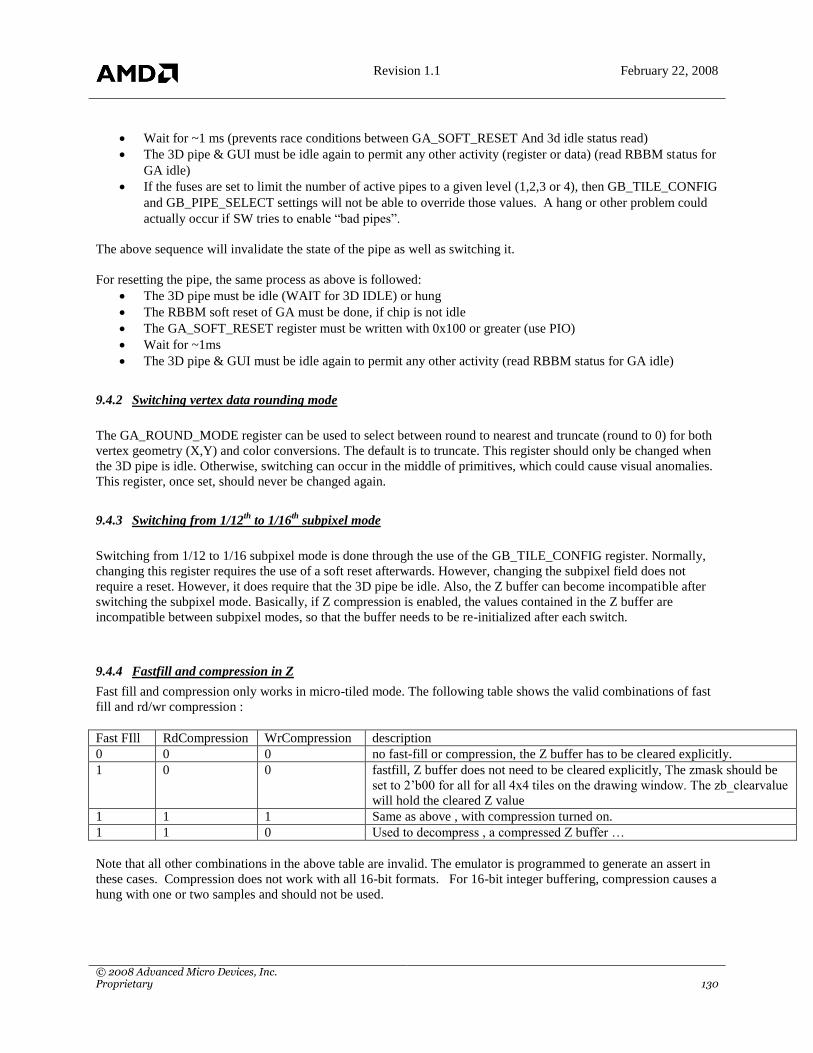
Revision 1.1 February 22, 2008
© 2008 Advanced Micro Devices, Inc. Proprietary 130
Wait for ~1 ms (prevents race conditions between GA_SOFT_RESET And 3d idle status read)
The 3D pipe & GUI must be idle again to permit any other activity (register or data) (read RBBM status for
GA idle)
If the fuses are set to limit the number of active pipes to a given level (1,2,3 or 4), then GB_TILE_CONFIG
and GB_PIPE_SELECT settings will not be able to override those values. A hang or other problem could
actually occur if SW tries to enable “bad pipes”.
The above sequence will invalidate the state of the pipe as well as switching it.
For resetting the pipe, the same process as above is followed:
The 3D pipe must be idle (WAIT for 3D IDLE) or hung
The RBBM soft reset of GA must be done, if chip is not idle
The GA_SOFT_RESET register must be written with 0x100 or greater (use PIO)
Wait for ~1ms
The 3D pipe & GUI must be idle again to permit any other activity (read RBBM status for GA idle)
9.4.2 Switching vertex data rounding mode
The GA_ROUND_MODE register can be used to select between round to nearest and truncate (round to 0) for both
vertex geometry (X,Y) and color conversions. The default is to truncate. This register should only be changed when
the 3D pipe is idle. Otherwise, switching can occur in the middle of primitives, which could cause visual anomalies.
This register, once set, should never be changed again.
9.4.3 Switching from 1/12th
to 1/16th
subpixel mode
Switching from 1/12 to 1/16 subpixel mode is done through the use of the GB_TILE_CONFIG register. Normally,
changing this register requires the use of a soft reset afterwards. However, changing the subpixel field does not
require a reset. However, it does require that the 3D pipe be idle. Also, the Z buffer can become incompatible after
switching the subpixel mode. Basically, if Z compression is enabled, the values contained in the Z buffer are
incompatible between subpixel modes, so that the buffer needs to be re-initialized after each switch.
9.4.4 Fastfill and compression in Z
Fast fill and compression only works in micro-tiled mode. The following table shows the valid combinations of fast
fill and rd/wr compression :
Fast FIll RdCompression WrCompression description
0 0 0 no fast-fill or compression, the Z buffer has to be cleared explicitly.
1 0 0 fastfill, Z buffer does not need to be cleared explicitly, The zmask should be
set to 2‟b00 for all for all 4x4 tiles on the drawing window. The zb_clearvalue
will hold the cleared Z value
1 1 1 Same as above , with compression turned on.
1 1 0 Used to decompress , a compressed Z buffer …
Note that all other combinations in the above table are invalid. The emulator is programmed to generate an assert in
these cases. Compression does not work with all 16-bit formats. For 16-bit integer buffering, compression causes a
hung with one or two samples and should not be used.

Revision 1.1 February 22, 2008
© 2008 Advanced Micro Devices, Inc. Proprietary 131
9.4.5 Z-Top
It is beneficial for performance to have Z buffer at the top of the pipe, since the quads that do not pass Z buffer do
not have to be sent to the shader. Depending on how many instructions the shader executes, this could gain you a lot
of advantage. There are several cases in which the Z buffer has to be at the bottom:
1- Alpha threshold (afunction) is turned on
2- Shader uses texkill instructions.
3- Chroma key cull enabled.
4- W-buffering
Cases 1,2 and 3 can kill a pixel before Z buffering . However, if the contents of the Z/stencil buffer will not be
modified, then ztop can remain enabled (1). This implies that the following state is in effect:
1- Z-buffering is disabled or Zwrite-mask is off .
2- Stencil is disabled or stencil-wrmask is off or SFAIL/ZPASS/ZFAIL are all set to KEEP.
W values are always generated at the bottom of the pipe, so for w-buffering, ztop should be set to 0.
There is penalty in moving the Z buffer from top to bottom or vice versa. The pipe will be stalled at the sc and all
the quads that are in the pipe between the sc and cb have to be processed before the switch occurs. This is all done in
HW. If the ztop =0 and you write another 0 to it, there is no performance penalty. If it is 1 and you write a 1 to it,
there is no performance penalty. The penalty is only incurred when you switch from top to bottom or bottom to top.
9.4.6 Sub-sample locations
In point sample mode, POS0 defines the X,Y of the upper left pixel of the quad. POS1 defines the X,Y of the upper
right pixel of a quad. POS2 defines the X,Y of the lower left pixel in a quad and POS3 defines the X,Y of the lower
right pixel in a quad. This is done so that in R200 style super-sampling mode, the sample locations for the pixels can
be jittered. Hierarcical Z has to be shut off when the 4 pixels in the quad have different locations in point sample
mode.
In multi-sample mode , samples 0,1,2,3,4,5 of pixels 0,1,2,3 of a quad are defines by pos0,1,2,3,4,5 .., so all pixels in
the quad have the same sub-sample pattern.
There is a quirk when setting the MSPOS0.msbd0_x. The value represents the distance from the left edge of the
pixel quad to the first sample in subpixels. All values less than eight should use the actual value, but „7‟ should be
used for the distance „8‟. The hardware will convert 7 into 8 internally.
It is also important that when using less than 6 multisample positions, the unused samples must be set to the position
of other valid samples.
9.4.7 Dithered Clears
Fast cmask clears of a subsampled buffer will not be dithered.
The ZB doesn‟t do color dithering so ZBCB clears will not be dithered.
When doing clears in 16 bit mode with dithering enabled the driver should examine the clear color value and
determine if it would be affected by dithering. For example a color value of zero when dithered will remain zero for
all dither factors. If the color would not be affected by dithering either fast clears or ZBCB clears can be used,
otherwise a full window rectangle write should be used to clear the buffer. This is only an issue for 16 bit buffers
with some clear color values so hardware support is not provided.
Revision 1.1 February 22, 2008
© 2008 Advanced Micro Devices, Inc. Proprietary 132
9.4.8 4x AA tiling
R420 introduced a new tiling mode for 4x AA buffers. Each 4x4 block of pixels occupies 8 cache lines of memory
(32 bytes per cache line). When the block is decompressed, the color samples are grouped together. Thus, all 16
sample 0s are in one chunk, all 16 sample 1s are in another, etc. On R300, decompressed blocks where organized
with sample 0s being first, then sample 1s, then 2s then 3s. On R420, groups of 8 cache lines have the top and
bottom halves interchanged when the block address is odd in the x dimension. For example, block (0,0) is organized
just like R300, but block (1,0) would have samples 2 and 3 before samples 0 and 1. Block (2, 0) would be just like
R300 again. Note: This new tiling mode only applies when memory mapping is disabled.
9.4.9 8x8 Z plane compression
Chips based on the RV350 and beyond support a new 8x8 Z plane compression mode specified in the
GB_Z_PEQ_CONFIG register. When compression is not enabled, the Z plane compression mode has to be set to
4x4 in order for the GA and ZB to agree on the Z plane equation format and avoid visual corruption.
9.5 Blend optimization notes
9.5.1 Disabling reads during blending
The destination color is not necessary for some blending operations. The cb has a read enable called
RB3D_BLENDCNTL.READ_ENABLE to control whether the destination color is read or not during blending
operations. Reads must be enabled during blending operations that require the destination color. Failure to do so
will result in incorrect results. Leaving the register enabled when blending is disabled does not have any adverse
affects.
9.5.2 Discarding pixels based upon the source color
There are cases where blend operations do not change the contents of the frame buffer. For example, adding zero to
the frame buffer does not change the frame buffer contents. Although the operations do nothing to the frame buffer,
they still take bandwidth. The cb can discard pixels based on the source color to eliminate some useless blend
operations. The RB3D_BLENDCNTL. DISCARD_SRC_PIXELS register controls the functionality. When to use
this feature is under driver control. The cb will not override this register if it is not safe to use under the current
blending mode.
9.5.3 ZB/CB cache flushes
ZB/CB cache flushes take hundreds of cycles to complete, so they should be avoided if possible. Performing a
cache flush when the cache is already clean only takes a cycle, so there isn‟t any penalty for flushing a cache
multiple times as long as there are no intervening quads.
9.6 Texture Notes
TX_CHROMA_KEY must be the same format as the texture being keyed with any unused msb‟s zero‟d. And
should be AVYU for all YUV formats.
TX_FMT_*_MPEG formats are implicitely signed. However the TX_FORMAT1_*_SIGNED_COMP* bits must
still be explicitely set. It is a bug to use an MPEG format and indicate that the components are unsigned.
Revision 1.1 February 22, 2008
© 2008 Advanced Micro Devices, Inc. Proprietary 133
9.7 Errata
9.7.1 Facing bit with Polymode & colors
In R5xx, just as R4xx, when lines are sent from the setup to the rasterizer, the setup‟s facing information is lost,
since no facing information is sent between the SU and SC. This implies that lines will always be treated as
“forward facing” in the scan converter. This facing information is passed to the shader as the “facing bit”, which can
be used as a conditional.
Consequently, in polygon outline mode, where lines have front and back meaning, when rendering a line polygon
(for either front or back), the facing bit will always be marked as front facing, regardless of the facing of the original
triangle. Back / Front culling does occur correctly here (i.e. if the front render is line and front face culling is
enabled, then no front facing lines will get drawn), but the facing bit for rendered lines or points will be always front
facing.
The R5xx contain a work-around for this problem, in the form of a special mode. This mode is enabled by setting
the bits of SU_PERF.PERF3_SEL to all 1‟s (31). When enabled, this will force the sign bits of the components of
the colors to be set to (0) for front facing, or (1) for back facing. All colors in a primitive will get their sign bit
changed, based on the facing of the primitive, or of its provoking vertex (in the case of polymode). If source colors
are positive, then, in the pixel shader, back facing polygons will have negative colors, while front facing polygons
will have positive colors. This mode will work, regardless of PS2 or PS3 mode in the pipe.
9.7.2 PS3 Polymode textures
In the R5xx mode, polymode texture coordinates are not computed correctly when the pipe is in PS3 mode. To fix
this, a polymode_ps3 fix has been implemented. This mode is enabled by setting the GA_PERF.PERF3_SEL[4] bit
to 0x1. This mode should only be set when in PS3 mode. As well, when set and in PS3 mode, colors will not
longer be computed correctly in polymode for polygons, but that is acceptable, since colors are not naturally
available in PS3 mode.
9.7.3 GA Fog stuffing
The GA supports stuffing the fog value (either an FP20 from C0a->C3a, or W or Z) into a texture component. The
limitation for R5xx, is that the GA can only stuff the component of the first active texture. It can only stuff any one
of the first 2 active components of the first active coordinate set.
9.7.4 Line rendering
When subpixel precision is enabled, there is a possibility that the rendering hardware will determine an incorrect
dominating direction, when the start and end X values of the line have the same 1/12 or 1/16 pixel value, but
different subpixel values. This can cause double pixel hits or missing pixels in continuous line drawing. The work-
around, is to disable subpixel precision rendering when drawing lines.
9.7.5 PS3_VTX_FMT & PS3_TEX_SOURCE
Writes to the PS3_VTX_FMT and PS3_TEX_SOURCE register can cause bad textures or hangs in R5xx chips, if
followed immediately by VF_CNTL writes (i.e. draw command). Following any of these 2 registers with 2 register
writes (to GA or any block below) will always avoid the problem, before the next VF_CNTL.

Revision 1.1 February 22, 2008
© 2008 Advanced Micro Devices, Inc. Proprietary 134
10. Registers
10.1 Color Buffer Registers
CB:RB3D_AARESOLVE_CTL · [R/W] · 32 bits · Access: 8/16/32 · MMReg:0x4e88
DESCRIPTION: Resolve Buffer Control. Unpipelined
Field Name Bits Default Description
AARESOLVE_MODE 0 0x0 Specifies if the color buffer is in resolve mode. The
cache must be empty before changing this register.
POSSIBLE VALUES:
00 - Normal operation.
01 - Resolve operation.
AARESOLVE_GAMMA 1 none Specifies the gamma and degamma to be applied to the
samples before and after filtering, respectively.
POSSIBLE VALUES:
00 - 1.0
01 - 2.2
AARESOLVE_ALPHA 2 0x0 Controls whether alpha is averaged in the resolve. 0 =>
the resolved alpha value is selected from the sample 0
value. 1=> the resolved alpha value is a filtered (average)
result of of the samples.
POSSIBLE VALUES:
00 - Resolved alpha value is taken from sample 0.
01 - Resolved alpha value is the average of the
samples. The average is not gamma corrected.
CB:RB3D_AARESOLVE_OFFSET · [R/W] · 32 bits · Access: 8/16/32 · MMReg:0x4e80
DESCRIPTION: Resolve buffer destination address. The cache must be empty before changing this register if the
cb is in resolve mode. Unpipelined
Field Name Bits Default Description
AARESOLVE_OFFSET 31:5 none 256-bit aligned 3D resolve destination offset.
CB:RB3D_AARESOLVE_PITCH · [R/W] · 32 bits · Access: 8/16/32 · MMReg:0x4e84
DESCRIPTION: Resolve Buffer Pitch and Tiling Control. The cache must be empty before changing this register if
the cb is in resolve mode. Unpipelined
Field Name Bits Default Description
AARESOLVE_PITCH 13:1 none 3D destination pitch in multiples of 2-pixels.

Revision 1.1 February 22, 2008
© 2008 Advanced Micro Devices, Inc. Proprietary 135
CB:RB3D_ABLENDCNTL · [R/W] · 32 bits · Access: 8/16/32 · MMReg:0x4e08
DESCRIPTION: Alpha Blend Control for Alpha Channel. Pipelined through the blender.
Field Name Bits Default Description
COMB_FCN 14:12 none Combine Function , Allows modification of how the
SRCBLEND and DESTBLEND are combined.
POSSIBLE VALUES:
00 - Add and Clamp
01 - Add but no Clamp
02 - Subtract Dst from Src, and Clamp
03 - Subtract Dst from Src, and don`t Clamp
04 - Minimum of Src, Dst (the src and dst blend
functions are forced to D3D_ONE)
05 - Maximum of Src, Dst (the src and dst blend
functions are forced to D3D_ONE)
06 - Subtract Src from Dst, and Clamp
07 - Subtract Src from Dst, and don`t Clamp
SRCBLEND 21:16 none Source Blend Function , Alpha blending function (SRC).
POSSIBLE VALUES:
00 - RESERVED
01 - D3D_ZERO
02 - D3D_ONE
03 - D3D_SRCCOLOR
04 - D3D_INVSRCCOLOR
05 - D3D_SRCALPHA
06 - D3D_INVSRCALPHA
07 - D3D_DESTALPHA
08 - D3D_INVDESTALPHA
09 - D3D_DESTCOLOR
10 - D3D_INVDESTCOLOR
11 - D3D_SRCALPHASAT
12 - D3D_BOTHSRCALPHA
13 - D3D_BOTHINVSRCALPHA
14 - RESERVED
15 - RESERVED
16 - RESERVED
17 - RESERVED
18 - RESERVED
19 - RESERVED
20 - RESERVED
21 - RESERVED
22 - RESERVED
23 - RESERVED
24 - RESERVED
25 - RESERVED
26 - RESERVED
27 - RESERVED
28 - RESERVED
29 - RESERVED
30 - RESERVED
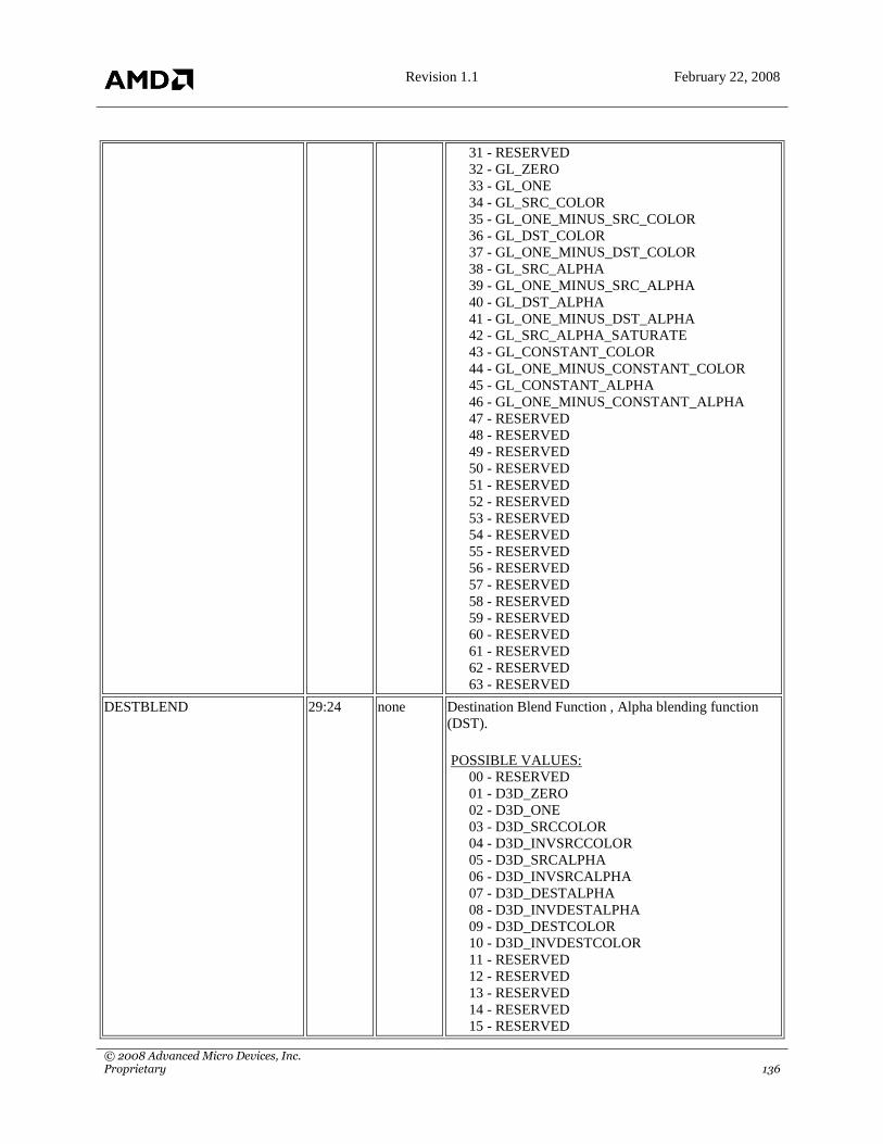
Revision 1.1 February 22, 2008
© 2008 Advanced Micro Devices, Inc. Proprietary 136
31 - RESERVED
32 - GL_ZERO
33 - GL_ONE
34 - GL_SRC_COLOR
35 - GL_ONE_MINUS_SRC_COLOR
36 - GL_DST_COLOR
37 - GL_ONE_MINUS_DST_COLOR
38 - GL_SRC_ALPHA
39 - GL_ONE_MINUS_SRC_ALPHA
40 - GL_DST_ALPHA
41 - GL_ONE_MINUS_DST_ALPHA
42 - GL_SRC_ALPHA_SATURATE
43 - GL_CONSTANT_COLOR
44 - GL_ONE_MINUS_CONSTANT_COLOR
45 - GL_CONSTANT_ALPHA
46 - GL_ONE_MINUS_CONSTANT_ALPHA
47 - RESERVED
48 - RESERVED
49 - RESERVED
50 - RESERVED
51 - RESERVED
52 - RESERVED
53 - RESERVED
54 - RESERVED
55 - RESERVED
56 - RESERVED
57 - RESERVED
58 - RESERVED
59 - RESERVED
60 - RESERVED
61 - RESERVED
62 - RESERVED
63 - RESERVED
DESTBLEND 29:24 none Destination Blend Function , Alpha blending function
(DST).
POSSIBLE VALUES:
00 - RESERVED
01 - D3D_ZERO
02 - D3D_ONE
03 - D3D_SRCCOLOR
04 - D3D_INVSRCCOLOR
05 - D3D_SRCALPHA
06 - D3D_INVSRCALPHA
07 - D3D_DESTALPHA
08 - D3D_INVDESTALPHA
09 - D3D_DESTCOLOR
10 - D3D_INVDESTCOLOR
11 - RESERVED
12 - RESERVED
13 - RESERVED
14 - RESERVED
15 - RESERVED

Revision 1.1 February 22, 2008
© 2008 Advanced Micro Devices, Inc. Proprietary 137
16 - RESERVED
17 - RESERVED
18 - RESERVED
19 - RESERVED
20 - RESERVED
21 - RESERVED
22 - RESERVED
23 - RESERVED
24 - RESERVED
25 - RESERVED
26 - RESERVED
27 - RESERVED
28 - RESERVED
29 - RESERVED
30 - RESERVED
31 - RESERVED
32 - GL_ZERO
33 - GL_ONE
34 - GL_SRC_COLOR
35 - GL_ONE_MINUS_SRC_COLOR
36 - GL_DST_COLOR
37 - GL_ONE_MINUS_DST_COLOR
38 - GL_SRC_ALPHA
39 - GL_ONE_MINUS_SRC_ALPHA
40 - GL_DST_ALPHA
41 - GL_ONE_MINUS_DST_ALPHA
42 - RESERVED
43 - GL_CONSTANT_COLOR
44 - GL_ONE_MINUS_CONSTANT_COLOR
45 - GL_CONSTANT_ALPHA
46 - GL_ONE_MINUS_CONSTANT_ALPHA
47 - RESERVED
48 - RESERVED
49 - RESERVED
50 - RESERVED
51 - RESERVED
52 - RESERVED
53 - RESERVED
54 - RESERVED
55 - RESERVED
56 - RESERVED
57 - RESERVED
58 - RESERVED
59 - RESERVED
60 - RESERVED
61 - RESERVED
62 - RESERVED
63 - RESERVED
CB:RB3D_BLENDCNTL · [R/W] · 32 bits · Access: 8/16/32 · MMReg:0x4e04
DESCRIPTION: Alpha Blend Control for Color Channels. Pipelined through the blender.

Revision 1.1 February 22, 2008
© 2008 Advanced Micro Devices, Inc. Proprietary 138
Field Name Bits Default Description
ALPHA_BLEND_ENABLE 0 0x0 Allow alpha blending with the destination.
POSSIBLE VALUES:
00 - Disable
01 - Enable
SEPARATE_ALPHA_ENABLE 1 0x0 Enables use of RB3D_ABLENDCNTL
POSSIBLE VALUES:
00 - Disabled (Use RB3D_BLENDCNTL)
01 - Enabled (Use RB3D_ABLENDCNTL)
READ_ENABLE 2 0x1 When blending is enabled, this enables memory reads.
Memory reads will still occur when this is disabled if
they are for reasons not related to blending.
POSSIBLE VALUES:
00 - Disable reads
01 - Enable reads
DISCARD_SRC_PIXELS 5:3 0x0 Discard pixels when blending is enabled based on the src
color.
POSSIBLE VALUES:
00 - Disable
01 - Discard pixels if src alpha <=
RB3D_DISCARD_SRC_PIXEL_LTE_THRESHOLD
02 - Discard pixels if src color <=
RB3D_DISCARD_SRC_PIXEL_LTE_THRESHOLD
03 - Discard pixels if src argb <=
RB3D_DISCARD_SRC_PIXEL_LTE_THRESHOLD
04 - Discard pixels if src alpha >=
RB3D_DISCARD_SRC_PIXEL_GTE_THRESHOLD
05 - Discard pixels if src color >=
RB3D_DISCARD_SRC_PIXEL_GTE_THRESHOLD
06 - Discard pixels if src argb >=
RB3D_DISCARD_SRC_PIXEL_GTE_THRESHOLD
07 - (reserved)
COMB_FCN 14:12 none Combine Function , Allows modification of how the
SRCBLEND and DESTBLEND are combined.
POSSIBLE VALUES:
00 - Add and Clamp
01 - Add but no Clamp
02 - Subtract Dst from Src, and Clamp
03 - Subtract Dst from Src, and don`t Clamp
04 - Minimum of Src, Dst (the src and dst blend
functions are forced to D3D_ONE)
05 - Maximum of Src, Dst (the src and dst blend
functions are forced to D3D_ONE)
06 - Subtract Src from Dst, and Clamp
07 - Subtract Src from Dst, and don`t Clamp

Revision 1.1 February 22, 2008
© 2008 Advanced Micro Devices, Inc. Proprietary 139
SRCBLEND 21:16 none Source Blend Function , Alpha blending function (SRC).
POSSIBLE VALUES:
00 - RESERVED
01 - D3D_ZERO
02 - D3D_ONE
03 - D3D_SRCCOLOR
04 - D3D_INVSRCCOLOR
05 - D3D_SRCALPHA
06 - D3D_INVSRCALPHA
07 - D3D_DESTALPHA
08 - D3D_INVDESTALPHA
09 - D3D_DESTCOLOR
10 - D3D_INVDESTCOLOR
11 - D3D_SRCALPHASAT
12 - D3D_BOTHSRCALPHA
13 - D3D_BOTHINVSRCALPHA
14 - RESERVED
15 - RESERVED
16 - RESERVED
17 - RESERVED
18 - RESERVED
19 - RESERVED
20 - RESERVED
21 - RESERVED
22 - RESERVED
23 - RESERVED
24 - RESERVED
25 - RESERVED
26 - RESERVED
27 - RESERVED
28 - RESERVED
29 - RESERVED
30 - RESERVED
31 - RESERVED
32 - GL_ZERO
33 - GL_ONE
34 - GL_SRC_COLOR
35 - GL_ONE_MINUS_SRC_COLOR
36 - GL_DST_COLOR
37 - GL_ONE_MINUS_DST_COLOR
38 - GL_SRC_ALPHA
39 - GL_ONE_MINUS_SRC_ALPHA
40 - GL_DST_ALPHA
41 - GL_ONE_MINUS_DST_ALPHA
42 - GL_SRC_ALPHA_SATURATE
43 - GL_CONSTANT_COLOR
44 - GL_ONE_MINUS_CONSTANT_COLOR
45 - GL_CONSTANT_ALPHA
46 - GL_ONE_MINUS_CONSTANT_ALPHA
47 - RESERVED
48 - RESERVED
49 - RESERVED

Revision 1.1 February 22, 2008
© 2008 Advanced Micro Devices, Inc. Proprietary 140
50 - RESERVED
51 - RESERVED
52 - RESERVED
53 - RESERVED
54 - RESERVED
55 - RESERVED
56 - RESERVED
57 - RESERVED
58 - RESERVED
59 - RESERVED
60 - RESERVED
61 - RESERVED
62 - RESERVED
63 - RESERVED
DESTBLEND 29:24 none Destination Blend Function , Alpha blending function
(DST).
POSSIBLE VALUES:
00 - RESERVED
01 - D3D_ZERO
02 - D3D_ONE
03 - D3D_SRCCOLOR
04 - D3D_INVSRCCOLOR
05 - D3D_SRCALPHA
06 - D3D_INVSRCALPHA
07 - D3D_DESTALPHA
08 - D3D_INVDESTALPHA
09 - D3D_DESTCOLOR
10 - D3D_INVDESTCOLOR
11 - RESERVED
12 - RESERVED
13 - RESERVED
14 - RESERVED
15 - RESERVED
16 - RESERVED
17 - RESERVED
18 - RESERVED
19 - RESERVED
20 - RESERVED
21 - RESERVED
22 - RESERVED
23 - RESERVED
24 - RESERVED
25 - RESERVED
26 - RESERVED
27 - RESERVED
28 - RESERVED
29 - RESERVED
30 - RESERVED
31 - RESERVED
32 - GL_ZERO
33 - GL_ONE
34 - GL_SRC_COLOR

Revision 1.1 February 22, 2008
© 2008 Advanced Micro Devices, Inc. Proprietary 141
35 - GL_ONE_MINUS_SRC_COLOR
36 - GL_DST_COLOR
37 - GL_ONE_MINUS_DST_COLOR
38 - GL_SRC_ALPHA
39 - GL_ONE_MINUS_SRC_ALPHA
40 - GL_DST_ALPHA
41 - GL_ONE_MINUS_DST_ALPHA
42 - RESERVED
43 - GL_CONSTANT_COLOR
44 - GL_ONE_MINUS_CONSTANT_COLOR
45 - GL_CONSTANT_ALPHA
46 - GL_ONE_MINUS_CONSTANT_ALPHA
47 - RESERVED
48 - RESERVED
49 - RESERVED
50 - RESERVED
51 - RESERVED
52 - RESERVED
53 - RESERVED
54 - RESERVED
55 - RESERVED
56 - RESERVED
57 - RESERVED
58 - RESERVED
59 - RESERVED
60 - RESERVED
61 - RESERVED
62 - RESERVED
63 - RESERVED
SRC_ALPHA_0_NO_READ 30 0x0 Enables source alpha zero performance optimization to
skip reads.
POSSIBLE VALUES:
00 - Disable source alpha zero performance
optimization to skip reads
01 - Enable source alpha zero performance
optimization to skip reads
SRC_ALPHA_1_NO_READ 31 0x0 Enables source alpha one performance optimization to
skip reads.
POSSIBLE VALUES:
00 - Disable source alpha one performance
optimization to skip reads
01 - Enable source alpha one performance
optimization to skip reads
CB:RB3D_DISCARD_SRC_PIXEL_GTE_THRESHOLD · [R/W] · 32 bits · Access: 8/16/32 ·
MMReg:0x4ea4
DESCRIPTION: Discard src pixels greater than or equal to threshold.
Field Name Bits Default Description

Revision 1.1 February 22, 2008
© 2008 Advanced Micro Devices, Inc. Proprietary 142
BLUE 7:0 0xFF Blue
GREEN 15:8 0xFF Green
RED 23:16 0xFF Red
ALPHA 31:24 0xFF Alpha
CB:RB3D_DISCARD_SRC_PIXEL_LTE_THRESHOLD · [R/W] · 32 bits · Access: 8/16/32 ·
MMReg:0x4ea0
DESCRIPTION: Discard src pixels less than or equal to threshold.
Field Name Bits Default Description
BLUE 7:0 0x0 Blue
GREEN 15:8 0x0 Green
RED 23:16 0x0 Red
ALPHA 31:24 0x0 Alpha
CB:RB3D_CCTL · [R/W] · 32 bits · Access: 8/16/32 · MMReg:0x4e00
DESCRIPTION: Unpipelined.
Field Name Bits Default Description
NUM_MULTIWRITES 6:5 0x0 A quad is replicated and written to this
many buffers.
POSSIBLE VALUES:
00 - 1 buffer. This is the only mode
where the cb processes the end of packet
command.
01 - 2 buffers
02 - 3 buffers
03 - 4 buffers
CLRCMP_FLIPE_ENABLE 7 0x0 Enables equivalent of rage128
CMP_EQ_FLIP color compare mode.
This is used to ensure 3D data does not
get chromakeyed away by logic in the
backend.
POSSIBLE VALUES:
00 - Disable color compare.
01 - Enable color compare.
AA_COMPRESSION_ENABLE 9 none Enables AA color compression. Cmask
must also be enabled when aa
compression is enabled. The cache must
be empty before this is changed.
POSSIBLE VALUES:
00 - Disable AA compression
01 - Enable AA compression
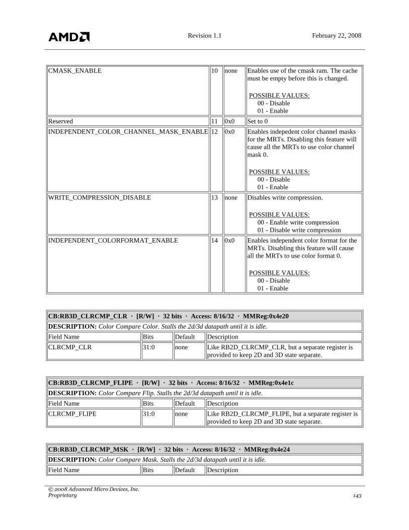
Revision 1.1 February 22, 2008
© 2008 Advanced Micro Devices, Inc. Proprietary 143
CMASK_ENABLE 10 none Enables use of the cmask ram. The cache
must be empty before this is changed.
POSSIBLE VALUES:
00 - Disable
01 - Enable
Reserved 11 0x0 Set to 0
INDEPENDENT_COLOR_CHANNEL_MASK_ENABLE 12 0x0 Enables indepedent color channel masks
for the MRTs. Disabling this feature will
cause all the MRTs to use color channel
mask 0.
POSSIBLE VALUES:
00 - Disable
01 - Enable
WRITE_COMPRESSION_DISABLE 13 none Disables write compression.
POSSIBLE VALUES:
00 - Enable write compression
01 - Disable write compression
INDEPENDENT_COLORFORMAT_ENABLE 14 0x0 Enables independent color format for the
MRTs. Disabling this feature will cause
all the MRTs to use color format 0.
POSSIBLE VALUES:
00 - Disable
01 - Enable
CB:RB3D_CLRCMP_CLR · [R/W] · 32 bits · Access: 8/16/32 · MMReg:0x4e20
DESCRIPTION: Color Compare Color. Stalls the 2d/3d datapath until it is idle.
Field Name Bits Default Description
CLRCMP_CLR 31:0 none Like RB2D_CLRCMP_CLR, but a separate register is
provided to keep 2D and 3D state separate.
CB:RB3D_CLRCMP_FLIPE · [R/W] · 32 bits · Access: 8/16/32 · MMReg:0x4e1c
DESCRIPTION: Color Compare Flip. Stalls the 2d/3d datapath until it is idle.
Field Name Bits Default Description
CLRCMP_FLIPE 31:0 none Like RB2D_CLRCMP_FLIPE, but a separate register is
provided to keep 2D and 3D state separate.
CB:RB3D_CLRCMP_MSK · [R/W] · 32 bits · Access: 8/16/32 · MMReg:0x4e24
DESCRIPTION: Color Compare Mask. Stalls the 2d/3d datapath until it is idle.
Field Name Bits Default Description

Revision 1.1 February 22, 2008
© 2008 Advanced Micro Devices, Inc. Proprietary 144
CLRCMP_MSK 31:0 none Like RB2D_CLRCMP_CLR, but separate registers
provided to keep 2D and 3D state separate.
CB:RB3D_COLOROFFSET[0-3] · [R/W] · 32 bits · Access: 8/16/32 · MMReg:0x4e28-0x4e34
DESCRIPTION: Color Buffer Address Offset of multibuffer 0. Unpipelined.
Field Name Bits Default Description
COLOROFFSET 31:5 none 256-bit aligned 3D destination offset address. The cache
must be empty before this is changed.
CB:RB3D_COLORPITCH[0-3] · [R/W] · 32 bits · Access: 8/16/32 · MMReg:0x4e38-0x4e44
DESCRIPTION: Color buffer format and tiling control for all the multibuffers and the pitch of multibuffer 0.
Unpipelined. The cache must be empty before any of the registers are changed.
Field Name Bits Default Description
COLORPITCH 13:1 none 3D destination pitch in multiples of 2-pixels.
COLORTILE 16 none Denotes whether the 3D destination is in macrotiled
format.
POSSIBLE VALUES:
00 - 3D destination is not macrotiled
01 - 3D destination is macrotiled
COLORMICROTILE 18:17 none Denotes whether the 3D destination is in microtiled
format.
POSSIBLE VALUES:
00 - 3D destination is no microtiled
01 - 3D destination is microtiled
02 - 3D destination is square microtiled. Only
available in 16-bit
03 - (reserved)
COLORENDIAN 20:19 none Specifies endian control for the color buffer.
POSSIBLE VALUES:
00 - No swap
01 - Word swap (2 bytes in 16-bit)
02 - Dword swap (4 bytes in a 32-bit)
03 - Half-Dword swap (2 16-bit in a 32-bit)
COLORFORMAT 24:21 0x6 3D destination color format.
POSSIBLE VALUES:
00 - ARGB10101010
01 - UV1010
02 - CI8 (2D ONLY)
03 - ARGB1555
04 - RGB565
05 - ARGB2101010
06 - ARGB8888

Revision 1.1 February 22, 2008
© 2008 Advanced Micro Devices, Inc. Proprietary 145
07 - ARGB32323232
08 - (Reserved)
09 - I8
10 - ARGB16161616
11 - YUV422 packed (VYUY)
12 - YUV422 packed (YVYU)
13 - UV88
14 - I10
15 - ARGB4444
CB:RB3D_COLOR_CHANNEL_MASK · [R/W] · 32 bits · Access: 8/16/32 · MMReg:0x4e0c
DESCRIPTION: 3D Color Channel Mask. If all the channels used in the current color format are disabled, then
the cb will discard all the incoming quads. Pipelined through the blender.
Field Name Bits Default Description
BLUE_MASK 0 0x1 mask bit for the blue channel
POSSIBLE VALUES:
00 - disable
01 - enable
GREEN_MASK 1 0x1 mask bit for the green channel
POSSIBLE VALUES:
00 - disable
01 - enable
RED_MASK 2 0x1 mask bit for the red channel
POSSIBLE VALUES:
00 - disable
01 - enable
ALPHA_MASK 3 0x1 mask bit for the alpha channel
POSSIBLE VALUES:
00 - disable
01 - enable
BLUE_MASK1 4 0x1 mask bit for the blue channel of MRT 1
POSSIBLE VALUES:
00 - disable
01 - enable
GREEN_MASK1 5 0x1 mask bit for the green channel of MRT 1
POSSIBLE VALUES:
00 - disable
01 - enable
RED_MASK1 6 0x1 mask bit for the red channel of MRT 1
POSSIBLE VALUES:

Revision 1.1 February 22, 2008
© 2008 Advanced Micro Devices, Inc. Proprietary 146
00 - disable
01 - enable
ALPHA_MASK1 7 0x1 mask bit for the alpha channel of MRT 1
POSSIBLE VALUES:
00 - disable
01 - enable
BLUE_MASK2 8 0x1 mask bit for the blue channel of MRT 2
POSSIBLE VALUES:
00 - disable
01 - enable
GREEN_MASK2 9 0x1 mask bit for the green channel of MRT 2
POSSIBLE VALUES:
00 - disable
01 - enable
RED_MASK2 10 0x1 mask bit for the red channel of MRT 2
POSSIBLE VALUES:
00 - disable
01 - enable
ALPHA_MASK2 11 0x1 mask bit for the alpha channel of MRT 2
POSSIBLE VALUES:
00 - disable
01 - enable
BLUE_MASK3 12 0x1 mask bit for the blue channel of MRT 3
POSSIBLE VALUES:
00 - disable
01 - enable
GREEN_MASK3 13 0x1 mask bit for the green channel of MRT 3
POSSIBLE VALUES:
00 - disable
01 - enable
RED_MASK3 14 0x1 mask bit for the red channel of MRT 3
POSSIBLE VALUES:
00 - disable
01 - enable
ALPHA_MASK3 15 0x1 mask bit for the alpha channel of MRT 3
POSSIBLE VALUES:
00 - disable
01 - enable

Revision 1.1 February 22, 2008
© 2008 Advanced Micro Devices, Inc. Proprietary 147
CB:RB3D_COLOR_CLEAR_VALUE · [R/W] · 32 bits · Access: 8/16/32 · MMReg:0x4e14
DESCRIPTION: Clear color that is used when the color mask is set to 00. Unpipelined. Program this register with
a 32-bit value in ARGB8888 or ARGB2101010 formats, ignoring the fields.
Field Name Bits Default Description
BLUE 7:0 none blue clear color
GREEN 15:8 none green clear color
RED 23:16 none red clear color
ALPHA 31:24 none alpha clear color
CB:RB3D_COLOR_CLEAR_VALUE_AR · [R/W] · 32 bits · Access: 8/16/32 · MMReg:0x46c0
DESCRIPTION: Alpha and red clear color values that are used when the color mask is set to 00 in FP16 per
component mode. Unpipelined.
Field Name Bits Default Description
RED 15:0 none red clear color
ALPHA 31:16 none alpha clear color
CB:RB3D_COLOR_CLEAR_VALUE_GB · [R/W] · 32 bits · Access: 8/16/32 · MMReg:0x46c4
DESCRIPTION: Green and blue clear color values that are used when the color mask is set to 00 in FP16 per
component mode. Unpipelined.
Field Name Bits Default Description
BLUE 15:0 none blue clear color
GREEN 31:16 none green clear color
CB:RB3D_CONSTANT_COLOR · [R/W] · 32 bits · Access: 8/16/32 · MMReg:0x4e10
DESCRIPTION: Constant color used by the blender. Pipelined through the blender.
Field Name Bits Default Description
BLUE 7:0 none blue constant color (For R520, this field is ignored, use
RB3D_CONSTANT_COLOR_GB__BLUE instead)
GREEN 15:8 none green constant color (For R520, this field is ignored, use
RB3D_CONSTANT_COLOR_GB__GREEN instead)
RED 23:16 none red constant color (For R520, this field is ignored, use
RB3D_CONSTANT_COLOR_AR__RED instead)
ALPHA 31:24 none alpha constant color (For R520, this field is ignored, use
RB3D_CONSTANT_COLOR_AR__ALPHA instead)
CB:RB3D_CONSTANT_COLOR_AR · [R/W] · 32 bits · Access: 8/16/32 · MMReg:0x4ef8
DESCRIPTION: Constant color used by the blender. Pipelined through the blender.
Field Name Bits Default Description
RED 15:0 none red constant color in 0.10 fixed or FP16 format

Revision 1.1 February 22, 2008
© 2008 Advanced Micro Devices, Inc. Proprietary 148
ALPHA 31:16 none alpha constant color in 0.10 fixed or FP16 format
CB:RB3D_CONSTANT_COLOR_GB · [R/W] · 32 bits · Access: 8/16/32 · MMReg:0x4efc
DESCRIPTION: Constant color used by the blender. Pipelined through the blender.
Field Name Bits Default Description
BLUE 15:0 none blue constant color in 0.10 fixed or FP16 format
GREEN 31:16 none green constant color in 0.10 fixed or FP16 format
CB:RB3D_DITHER_CTL · [R/W] · 32 bits · Access: 8/16/32 · MMReg:0x4e50
DESCRIPTION: Dithering control register. Pipelined through the blender.
Field Name Bits Default Description
DITHER_MODE 1:0 0x0 Dither mode
POSSIBLE VALUES:
00 - Truncate
01 - Round
02 - LUT dither
03 - (reserved)
ALPHA_DITHER_MODE 3:2 0x0 POSSIBLE VALUES:
00 - Truncate
01 - Round
02 - LUT dither
03 - (reserved)
CB:RB3D_DSTCACHE_CTLSTAT · [R/W] · 32 bits · Access: 8/16/32 · MMReg:0x4e4c
DESCRIPTION: Destination Color Buffer Cache Control/Status. If the cb is in e2 mode, then a flush or free will
not occur upon a write to this register, but a sync will be immediately sent if one is requested. If both DC_FLUSH
and DC_FREE are zero but DC_FINISH is one, then a sync will be sent immediately -- the cb will not wait for all
the previous operations to complete before sending the sync. Unpipelined except when DC_FINISH and DC_FREE
are both set to zero.
Field Name Bits Default Description
DC_FLUSH 1:0 0x0 Setting this bit flushes dirty data from the 3D Dst Cache.
Unless the DC_FREE bits are also set, the tags in the
cache remain valid. A purge is achieved by setting both
DC_FLUSH and DC_FREE.
POSSIBLE VALUES:
00 - No effect
01 - No effect
02 - Flushes dirty 3D data
03 - Flushes dirty 3D data
DC_FREE 3:2 0x0 Setting this bit invalidates the 3D Dst Cache tags. Unless
the DC_FLUSH bit is also set, the cache lines are not
written to memory. A purge is achieved by setting both
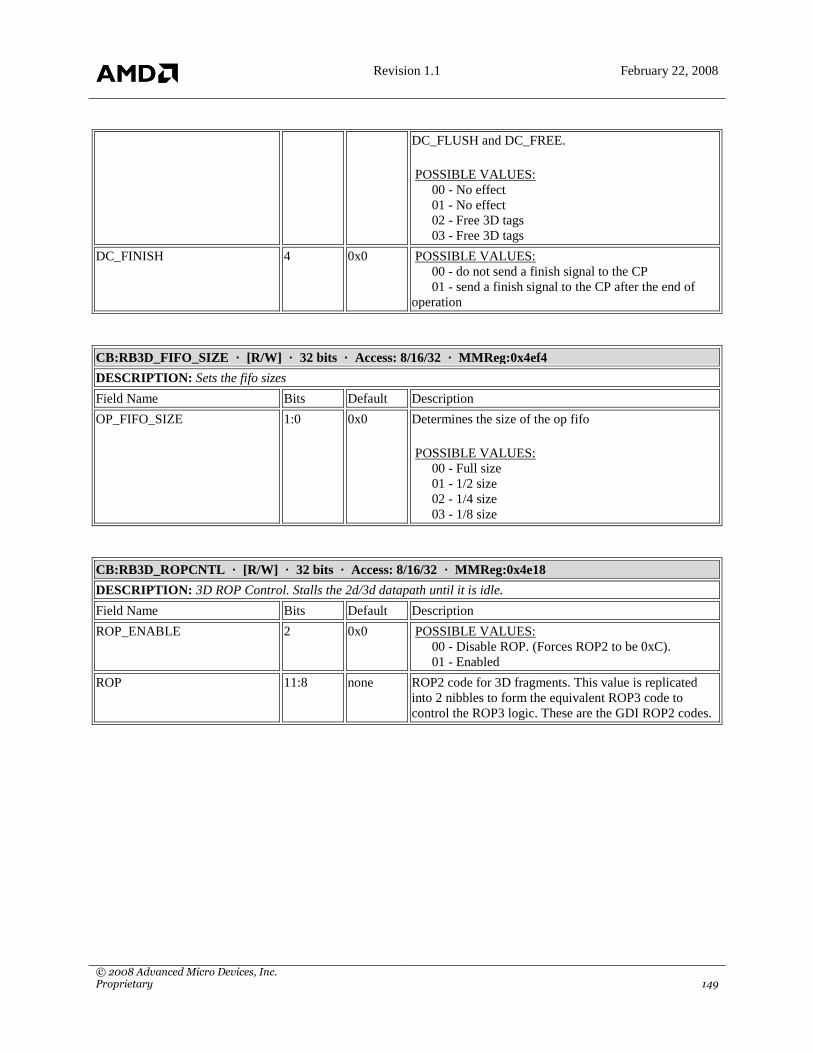
Revision 1.1 February 22, 2008
© 2008 Advanced Micro Devices, Inc. Proprietary 149
DC_FLUSH and DC_FREE.
POSSIBLE VALUES:
00 - No effect
01 - No effect
02 - Free 3D tags
03 - Free 3D tags
DC_FINISH 4 0x0 POSSIBLE VALUES:
00 - do not send a finish signal to the CP
01 - send a finish signal to the CP after the end of
operation
CB:RB3D_FIFO_SIZE · [R/W] · 32 bits · Access: 8/16/32 · MMReg:0x4ef4
DESCRIPTION: Sets the fifo sizes
Field Name Bits Default Description
OP_FIFO_SIZE 1:0 0x0 Determines the size of the op fifo
POSSIBLE VALUES:
00 - Full size
01 - 1/2 size
02 - 1/4 size
03 - 1/8 size
CB:RB3D_ROPCNTL · [R/W] · 32 bits · Access: 8/16/32 · MMReg:0x4e18
DESCRIPTION: 3D ROP Control. Stalls the 2d/3d datapath until it is idle.
Field Name Bits Default Description
ROP_ENABLE 2 0x0 POSSIBLE VALUES:
00 - Disable ROP. (Forces ROP2 to be 0xC).
01 - Enabled
ROP 11:8 none ROP2 code for 3D fragments. This value is replicated
into 2 nibbles to form the equivalent ROP3 code to
control the ROP3 logic. These are the GDI ROP2 codes.

Revision 1.1 February 22, 2008
© 2008 Advanced Micro Devices, Inc. Proprietary 150
10.2 Fog Registers
FG:FG_ALPHA_FUNC · [R/W] · 32 bits · Access: 8/16/32 · MMReg:0x4bd4
DESCRIPTION: Alpha Function
Field Name Bits Default Description
AF_VAL 7:0 0x0 Specifies the 8-bit alpha compare value when
AF_EN_8BIT is enabled
AF_FUNC 10:8 0x0 Specifies the alpha compare function.
POSSIBLE VALUES:
00 - AF_NEVER
01 - AF_LESS
02 - AF_EQUAL
03 - AF_LE
04 - AF_GREATER
05 - AF_NOTEQUAL
06 - AF_GE
07 - AF_ALWAYS
AF_EN 11 0x0 Enables/Disables alpha compare function.
POSSIBLE VALUES:
00 - Disable alpha function.
01 - Enable alpha function.
AF_EN_8BIT 12 0x0 Enable 8-bit alpha compare function.
POSSIBLE VALUES:
00 - Default 10-bit alpha compare.
01 - Enable 8-bit alpha compare.
AM_EN 16 0x0 Enables/Disables alpha-to-mask function.
POSSIBLE VALUES:
00 - Disable alpha to mask function.
01 - Enable alpha to mask function.
AM_CFG 17 0x0 Specfies number of sub-pixel samples for alpha-to-mask
function.
POSSIBLE VALUES:
00 - 2/4 sub-pixel samples.
01 - 3/6 sub-pixel samples.
DITH_EN 20 0x0 Enables/Disables RGB Dithering (Not supported in
R520)
POSSIBLE VALUES:
00 - Disable Dithering
01 - Enable Dithering.
ALP_OFF_EN 24 0x0 Alpha offset enable/disable (Not supported in R520)

Revision 1.1 February 22, 2008
© 2008 Advanced Micro Devices, Inc. Proprietary 151
POSSIBLE VALUES:
00 - Disables alpha offset of 2 (default r300 & rv350
behavior)
01 - Enables offset of 2 on alpha coming in from the
US
DISCARD_ZERO_MASK_QUAD 25 0x0 Enable/Disable discard zero mask coverage quad to ZB
POSSIBLE VALUES:
00 - No discard of zero coverage mask quads
01 - Discard zero coverage mask quads
FP16_ENABLE 28 0x0 Enables/Disables FP16 alpha function
POSSIBLE VALUES:
00 - Default 10-bit alpha compare and alpha-to-mask
function
01 - Enable FP16 alpha compare and alpha-to-mask
function
FG:FG_ALPHA_VALUE · [R/W] · 32 bits · Access: 8/16/32 · MMReg:0x4be0
DESCRIPTION: Alpha Compare Value
Field Name Bits Default Description
AF_VAL 15:0 0x0 Specifies the alpha compare value, 0.10 fixed or FP16
format
FG:FG_DEPTH_SRC · [R/W] · 32 bits · Access: 8/16/32 · MMReg:0x4bd8
DESCRIPTION: Where does depth come from?
Field Name Bits Default Description
DEPTH_SRC 0 0x0 POSSIBLE VALUES:
00 - Depth comes from scan converter as plane
equation.
01 - Depth comes from shader as four discrete values.
FG:FG_FOG_BLEND · [R/W] · 32 bits · Access: 8/16/32 · MMReg:0x4bc0
DESCRIPTION: Fog Blending Enable
Field Name Bits Default Description
ENABLE 0 0x0 Enable for fog blending
POSSIBLE VALUES:
00 - Disables fog (output matches input color).
01 - Enables fog.
FN 2:1 0x0 Fog generation function

Revision 1.1 February 22, 2008
© 2008 Advanced Micro Devices, Inc. Proprietary 152
POSSIBLE VALUES:
00 - Fog function is linear
01 - Fog function is exponential
02 - Fog function is exponential squared
03 - Fog is derived from constant fog factor
FG:FG_FOG_COLOR_B · [R/W] · 32 bits · Access: 8/16/32 · MMReg:0x4bd0
DESCRIPTION: Blue Component of Fog Color
Field Name Bits Default Description
BLUE 9:0 0x0 Blue component of fog color; (0.10) fixed format.
FG:FG_FOG_COLOR_G · [R/W] · 32 bits · Access: 8/16/32 · MMReg:0x4bcc
DESCRIPTION: Green Component of Fog Color
Field Name Bits Default Description
GREEN 9:0 0x0 Green component of fog color; (0.10) fixed format.
FG:FG_FOG_COLOR_R · [R/W] · 32 bits · Access: 8/16/32 · MMReg:0x4bc8
DESCRIPTION: Red Component of Fog Color
Field Name Bits Default Description
RED 9:0 0x0 Red component of fog color; (0.10) fixed format.
FG:FG_FOG_FACTOR · [R/W] · 32 bits · Access: 8/16/32 · MMReg:0x4bc4
DESCRIPTION: Constant Factor for Fog Blending
Field Name Bits Default Description
FACTOR 9:0 0x0 Constant fog factor; fixed (0.10) format.

Revision 1.1 February 22, 2008
© 2008 Advanced Micro Devices, Inc. Proprietary 153
10.3 Geometry Assembly Registers
GA:GA_COLOR_CONTROL · [R/W] · 32 bits · Access: 8/16/32 · MMReg:0x4278
DESCRIPTION: Specifies per RGB or Alpha shading method.
Field Name Bits Default Description
RGB0_SHADING 1:0 0x0 Specifies solid, flat or Gouraud shading.
POSSIBLE VALUES:
00 - Solid fill color
01 - Flat shading
02 - Gouraud shading
ALPHA0_SHADING 3:2 0x0 Specifies solid, flat or Gouraud shading.
POSSIBLE VALUES:
00 - Solid fill color
01 - Flat shading
02 - Gouraud shading
RGB1_SHADING 5:4 0x0 Specifies solid, flat or Gouraud shading.
POSSIBLE VALUES:
00 - Solid fill color
01 - Flat shading
02 - Gouraud shading
ALPHA1_SHADING 7:6 0x0 Specifies solid, flat or Gouraud shading.
POSSIBLE VALUES:
00 - Solid fill color
01 - Flat shading
02 - Gouraud shading
RGB2_SHADING 9:8 0x0 Specifies solid, flat or Gouraud shading.
POSSIBLE VALUES:
00 - Solid fill color
01 - Flat shading
02 - Gouraud shading
ALPHA2_SHADING 11:10 0x0 Specifies solid, flat or Gouraud shading.
POSSIBLE VALUES:
00 - Solid fill color
01 - Flat shading
02 - Gouraud shading
RGB3_SHADING 13:12 0x0 Specifies solid, flat or Gouraud shading.
POSSIBLE VALUES:
00 - Solid fill color
01 - Flat shading
02 - Gouraud shading

Revision 1.1 February 22, 2008
© 2008 Advanced Micro Devices, Inc. Proprietary 154
ALPHA3_SHADING 15:14 0x0 Specifies solid, flat or Gouraud shading.
POSSIBLE VALUES:
00 - Solid fill color
01 - Flat shading
02 - Gouraud shading
PROVOKING_VERTEX 17:16 0x0 Specifies, for flat shaded polygons, which vertex holds
the polygon color.
POSSIBLE VALUES:
00 - Provoking is first vertex
01 - Provoking is second vertex
02 - Provoking is third vertex
03 - Provoking is always last vertex
GA:GA_COLOR_CONTROL_PS3 · [R/W] · 32 bits · Access: 8/16/32 · MMReg:0x4258
DESCRIPTION: Specifies color properties and mappings of textures.
Field Name Bits Default Description
TEX0_SHADING_PS3 1:0 0x0 Specifies undefined(0), flat(1) and Gouraud(2/def)
shading for each texture.
POSSIBLE VALUES:
00 - Solid fill color
01 - Flat shading
02 - Gouraud shading
TEX1_SHADING_PS3 3:2 0x0 Specifies undefined(0), flat(1) and Gouraud(2/def)
shading for each texture.
POSSIBLE VALUES:
00 - Solid fill color
01 - Flat shading
02 - Gouraud shading
TEX2_SHADING_PS3 5:4 0x0 Specifies undefined(0), flat(1) and Gouraud(2/def)
shading for each texture.
POSSIBLE VALUES:
00 - Solid fill color
01 - Flat shading
02 - Gouraud shading
TEX3_SHADING_PS3 7:6 0x0 Specifies undefined(0), flat(1) and Gouraud(2/def)
shading for each texture.
POSSIBLE VALUES:
00 - Solid fill color
01 - Flat shading
02 - Gouraud shading
TEX4_SHADING_PS3 9:8 0x0 Specifies undefined(0), flat(1) and Gouraud(2/def)
shading for each texture.
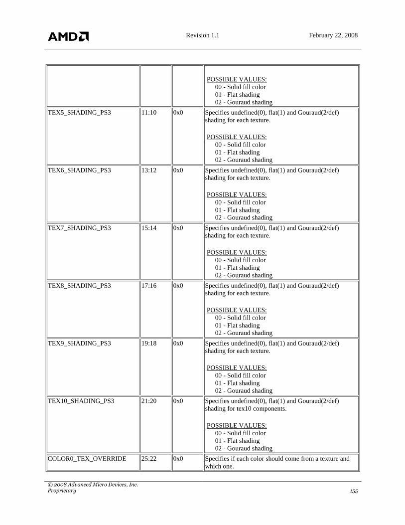
Revision 1.1 February 22, 2008
© 2008 Advanced Micro Devices, Inc. Proprietary 155
POSSIBLE VALUES:
00 - Solid fill color
01 - Flat shading
02 - Gouraud shading
TEX5_SHADING_PS3 11:10 0x0 Specifies undefined(0), flat(1) and Gouraud(2/def)
shading for each texture.
POSSIBLE VALUES:
00 - Solid fill color
01 - Flat shading
02 - Gouraud shading
TEX6_SHADING_PS3 13:12 0x0 Specifies undefined(0), flat(1) and Gouraud(2/def)
shading for each texture.
POSSIBLE VALUES:
00 - Solid fill color
01 - Flat shading
02 - Gouraud shading
TEX7_SHADING_PS3 15:14 0x0 Specifies undefined(0), flat(1) and Gouraud(2/def)
shading for each texture.
POSSIBLE VALUES:
00 - Solid fill color
01 - Flat shading
02 - Gouraud shading
TEX8_SHADING_PS3 17:16 0x0 Specifies undefined(0), flat(1) and Gouraud(2/def)
shading for each texture.
POSSIBLE VALUES:
00 - Solid fill color
01 - Flat shading
02 - Gouraud shading
TEX9_SHADING_PS3 19:18 0x0 Specifies undefined(0), flat(1) and Gouraud(2/def)
shading for each texture.
POSSIBLE VALUES:
00 - Solid fill color
01 - Flat shading
02 - Gouraud shading
TEX10_SHADING_PS3 21:20 0x0 Specifies undefined(0), flat(1) and Gouraud(2/def)
shading for tex10 components.
POSSIBLE VALUES:
00 - Solid fill color
01 - Flat shading
02 - Gouraud shading
COLOR0_TEX_OVERRIDE 25:22 0x0 Specifies if each color should come from a texture and
which one.

Revision 1.1 February 22, 2008
© 2008 Advanced Micro Devices, Inc. Proprietary 156
POSSIBLE VALUES:
00 - No override
01 - Stuff texture 0
02 - Stuff texture 1
03 - Stuff texture 2
04 - Stuff texture 3
05 - Stuff texture 4
06 - Stuff texture 5
07 - Stuff texture 6
08 - Stuff texture 7
09 - Stuff texture 8/C2
10 - Stuff texture 9/C3
COLOR1_TEX_OVERRIDE 29:26 0x0 Specifies if each color should come from a texture and
which one.
POSSIBLE VALUES:
00 - No override
01 - Stuff texture 0
02 - Stuff texture 1
03 - Stuff texture 2
04 - Stuff texture 3
05 - Stuff texture 4
06 - Stuff texture 5
07 - Stuff texture 6
08 - Stuff texture 7
09 - Stuff texture 8/C2
10 - Stuff texture 9/C3
GA:GA_ENHANCE · [R/W] · 32 bits · Access: 8/16/32 · MMReg:0x4274
DESCRIPTION: GA Enhancement Register
Field Name Bits Default Description
DEADLOCK_CNTL 0 0x0 TCL/GA Deadlock control.
POSSIBLE VALUES:
00 - No effect.
01 - Prevents TCL interface from deadlocking on GA
side.
FASTSYNC_CNTL 1 0x1 Enables Fast register/primitive switching
POSSIBLE VALUES:
00 - No effect.
01 - Enables high-performance register/primitive
switching.
REG_READWRITE 2 0x0 R520+: When set, GA supports simultaneous register
reads & writes
POSSIBLE VALUES:

Revision 1.1 February 22, 2008
© 2008 Advanced Micro Devices, Inc. Proprietary 157
00 - No effect.
01 - Enables GA support of simultaneous register
reads and writes.
REG_NOSTALL 3 0x0 POSSIBLE VALUES:
00 - No effect.
01 - Enables GA support of no-stall reads for register
read back.
GA:GA_FIFO_CNTL · [R/W] · 32 bits · Access: 8/16/32 · MMReg:0x4270
DESCRIPTION: GA Input fifo high water marks
Field Name Bits Default Description
VERTEX_FIFO 2:0 0x0 Number of words remaining in input vertex fifo before
asserting nearly full
INDEX_FIFO 5:3 0x0 Number of words remaining in input primitive fifo
before asserting nearly full
REG_FIFO 13:6 0x0 Number of words remaining in input register fifo before
asserting nearly full
GA:GA_FILL_A · [R/W] · 32 bits · Access: 8/16/32 · MMReg:0x422c
DESCRIPTION: Alpha fill color
Field Name Bits Default Description
COLOR_ALPHA 31:0 0x0 FP20 format for alpha fill.
GA:GA_FILL_B · [R/W] · 32 bits · Access: 8/16/32 · MMReg:0x4228
DESCRIPTION: Blue fill color
Field Name Bits Default Description
COLOR_BLUE 31:0 0x0 FP20 format for blue fill.
GA:GA_FILL_G · [R/W] · 32 bits · Access: 8/16/32 · MMReg:0x4224
DESCRIPTION: Green fill color
Field Name Bits Default Description
COLOR_GREEN 31:0 0x0 FP20 format for green fill.
GA:GA_FILL_R · [R/W] · 32 bits · Access: 8/16/32 · MMReg:0x4220
DESCRIPTION: Red fill color
Field Name Bits Default Description
COLOR_RED 31:0 0x0 FP20 format for red fill.

Revision 1.1 February 22, 2008
© 2008 Advanced Micro Devices, Inc. Proprietary 158
GA:GA_FOG_OFFSET · [R/W] · 32 bits · Access: 8/16/32 · MMReg:0x4298
DESCRIPTION: Specifies the offset to apply to fog.
Field Name Bits Default Description
VALUE 31:0 0x0 32b SPFP scale value.
GA:GA_FOG_SCALE · [R/W] · 32 bits · Access: 8/16/32 · MMReg:0x4294
DESCRIPTION: Specifies the scale to apply to fog.
Field Name Bits Default Description
VALUE 31:0 0x0 32b SPFP scale value.
GA:GA_IDLE · [R/W] · 32 bits · Access: 8/16/32 · MMReg:0x425c
DESCRIPTION: Returns idle status of various G3D block, captured when GA_IDLE written or when hard or soft
reset asserted.
Field Name Bits Default Description
PIPE3_Z_IDLE 0 0x0 Idle status of physical pipe 3 Z unit
PIPE2_Z_IDLE 1 0x0 Idle status of physical pipe 2 Z unit
PIPE3_CB_IDLE 2 0x0 Idle status of physical pipe 3 CB unit
PIPE2_CB_IDLE 3 0x0 Idle status of physical pipe 2 CB unit
PIPE3_FG_IDLE 4 0x0 Idle status of physical pipe 3 FG unit
PIPE2_FG_IDLE 5 0x0 Idle status of physical pipe 2 FG unit
PIPE3_US_IDLE 6 0x0 Idle status of physical pipe 3 US unit
PIPE2_US_IDLE 7 0x0 Idle status of physical pipe 2 US unit
PIPE3_SC_IDLE 8 0x0 Idle status of physical pipe 3 SC unit
PIPE2_SC_IDLE 9 0x0 Idle status of physical pipe 2 SC unit
PIPE3_RS_IDLE 10 0x0 Idle status of physical pipe 3 RS unit
PIPE2_RS_IDLE 11 0x0 Idle status of physical pipe 2 RS unit
PIPE1_Z_IDLE 12 0x0 Idle status of physical pipe 1 Z unit
PIPE0_Z_IDLE 13 0x0 Idle status of physical pipe 0 Z unit
PIPE1_CB_IDLE 14 0x0 Idle status of physical pipe 1 CB unit
PIPE0_CB_IDLE 15 0x0 Idle status of physical pipe 0 CB unit
PIPE1_FG_IDLE 16 0x0 Idle status of physical pipe 1 FG unit
PIPE0_FG_IDLE 17 0x0 Idle status of physical pipe 0 FG unit
PIPE1_US_IDLE 18 0x0 Idle status of physical pipe 1 US unit
PIPE0_US_IDLE 19 0x0 Idle status of physical pipe 0 US unit
PIPE1_SC_IDLE 20 0x0 Idle status of physical pipe 1 SC unit
PIPE0_SC_IDLE 21 0x0 Idle status of physical pipe 0 SC unit
PIPE1_RS_IDLE 22 0x0 Idle status of physical pipe 1 RS unit
PIPE0_RS_IDLE 23 0x0 Idle status of physical pipe 0 RS unit
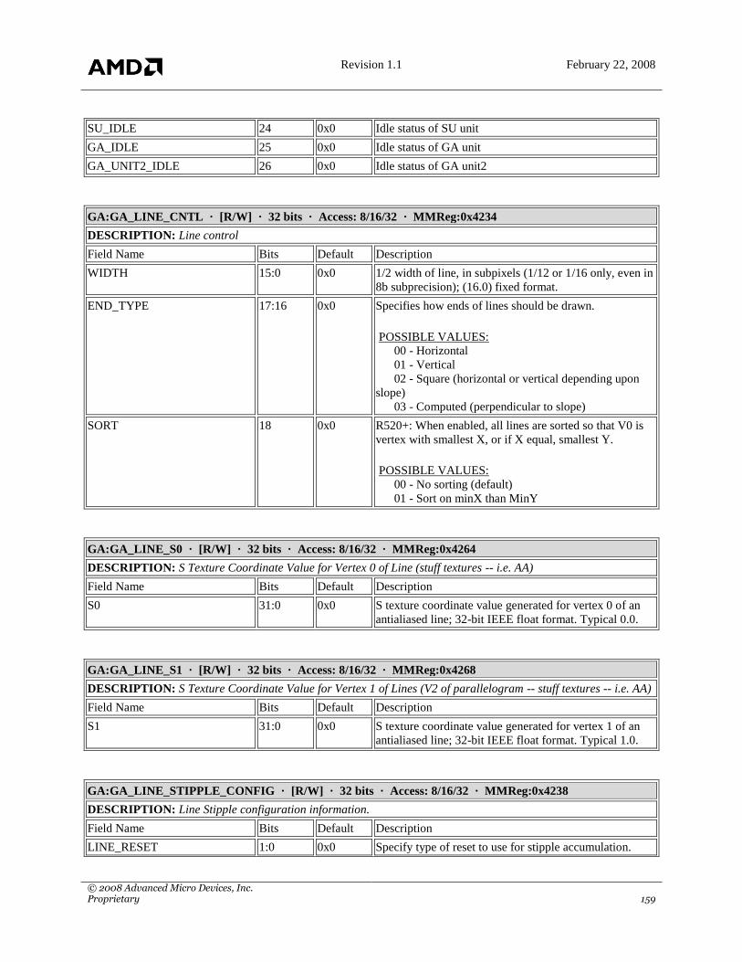
Revision 1.1 February 22, 2008
© 2008 Advanced Micro Devices, Inc. Proprietary 159
SU_IDLE 24 0x0 Idle status of SU unit
GA_IDLE 25 0x0 Idle status of GA unit
GA_UNIT2_IDLE 26 0x0 Idle status of GA unit2
GA:GA_LINE_CNTL · [R/W] · 32 bits · Access: 8/16/32 · MMReg:0x4234
DESCRIPTION: Line control
Field Name Bits Default Description
WIDTH 15:0 0x0 1/2 width of line, in subpixels (1/12 or 1/16 only, even in
8b subprecision); (16.0) fixed format.
END_TYPE 17:16 0x0 Specifies how ends of lines should be drawn.
POSSIBLE VALUES:
00 - Horizontal
01 - Vertical
02 - Square (horizontal or vertical depending upon
slope)
03 - Computed (perpendicular to slope)
SORT 18 0x0 R520+: When enabled, all lines are sorted so that V0 is
vertex with smallest X, or if X equal, smallest Y.
POSSIBLE VALUES:
00 - No sorting (default)
01 - Sort on minX than MinY
GA:GA_LINE_S0 · [R/W] · 32 bits · Access: 8/16/32 · MMReg:0x4264
DESCRIPTION: S Texture Coordinate Value for Vertex 0 of Line (stuff textures -- i.e. AA)
Field Name Bits Default Description
S0 31:0 0x0 S texture coordinate value generated for vertex 0 of an
antialiased line; 32-bit IEEE float format. Typical 0.0.
GA:GA_LINE_S1 · [R/W] · 32 bits · Access: 8/16/32 · MMReg:0x4268
DESCRIPTION: S Texture Coordinate Value for Vertex 1 of Lines (V2 of parallelogram -- stuff textures -- i.e. AA)
Field Name Bits Default Description
S1 31:0 0x0 S texture coordinate value generated for vertex 1 of an
antialiased line; 32-bit IEEE float format. Typical 1.0.
GA:GA_LINE_STIPPLE_CONFIG · [R/W] · 32 bits · Access: 8/16/32 · MMReg:0x4238
DESCRIPTION: Line Stipple configuration information.
Field Name Bits Default Description
LINE_RESET 1:0 0x0 Specify type of reset to use for stipple accumulation.

Revision 1.1 February 22, 2008
© 2008 Advanced Micro Devices, Inc. Proprietary 160
POSSIBLE VALUES:
00 - No reseting
01 - Reset per line
02 - Reset per packet
STIPPLE_SCALE 31:2 0x0 Specifies, in truncated (30b) floating point, scale to apply
to generated texture coordinates.
GA:GA_LINE_STIPPLE_VALUE · [R/W] · 32 bits · Access: 8/16/32 · MMReg:0x4260
DESCRIPTION: Current value of stipple accumulator.
Field Name Bits Default Description
STIPPLE_VALUE 31:0 0x0 24b Integer, measuring stipple accumulation in subpixels
(1/12 or 1/16, even in 8b precision). (note: field is 32b,
but only lower 24b used)
GA:GA_OFFSET · [R/W] · 32 bits · Access: 8/16/32 · MMReg:0x4290
DESCRIPTION: Specifies x & y offsets for vertex data after conversion to FP.
Field Name Bits Default Description
X_OFFSET 15:0 0x0 Specifies X offset in S15 format (subpixels -- 1/12 or
1/16, even in 8b subprecision).
Y_OFFSET 31:16 0x0 Specifies Y offset in S15 format (subpixels -- 1/12 or
1/16, even in 8b subprecision).
GA:GA_POINT_MINMAX · [R/W] · 32 bits · Access: 8/16/32 · MMReg:0x4230
DESCRIPTION: Specifies maximum and minimum point & sprite sizes for per vertex size specification.
Field Name Bits Default Description
MIN_SIZE 15:0 0x0 Minimum point & sprite radius (in subsamples) size to
allow.
MAX_SIZE 31:16 0x0 Maximum point & sprite radius (in subsamples) size to
allow.
GA:GA_POINT_S0 · [R/W] · 32 bits · Access: 8/16/32 · MMReg:0x4200
DESCRIPTION: S Texture Coordinate of Vertex 0 for Point texture stuffing (LLC)
Field Name Bits Default Description
S0 31:0 0x0 S texture coordinate of vertex 0 for point; 32-bit IEEE
float format.
GA:GA_POINT_S1 · [R/W] · 32 bits · Access: 8/16/32 · MMReg:0x4208
DESCRIPTION: S Texture Coordinate of Vertex 2 for Point texture stuffing (URC)

Revision 1.1 February 22, 2008
© 2008 Advanced Micro Devices, Inc. Proprietary 161
Field Name Bits Default Description
S1 31:0 0x0 S texture coordinate of vertex 2 for point; 32-bit IEEE
float format.
GA:GA_POINT_SIZE · [R/W] · 32 bits · Access: 8/16/32 · MMReg:0x421c
DESCRIPTION: Dimensions for Points
Field Name Bits Default Description
HEIGHT 15:0 0x0 1/2 Height of point; fixed (16.0), subpixel format (1/12
or 1/16, even if in 8b precision).
WIDTH 31:16 0x0 1/2 Width of point; fixed (16.0), subpixel format (1/12 or
1/16, even if in 8b precision)
GA:GA_POINT_T0 · [R/W] · 32 bits · Access: 8/16/32 · MMReg:0x4204
DESCRIPTION: T Texture Coordinate of Vertex 0 for Point texture stuffing (LLC)
Field Name Bits Default Description
T0 31:0 0x0 T texture coordinate of vertex 0 for point; 32-bit IEEE
float format.
GA:GA_POINT_T1 · [R/W] · 32 bits · Access: 8/16/32 · MMReg:0x420c
DESCRIPTION: T Texture Coordinate of Vertex 2 for Point texture stuffing (URC)
Field Name Bits Default Description
T1 31:0 0x0 T texture coordinate of vertex 2 for point; 32-bit IEEE
float format.
GA:GA_POLY_MODE · [R/W] · 32 bits · Access: 8/16/32 · MMReg:0x4288
DESCRIPTION: Polygon Mode
Field Name Bits Default Description
POLY_MODE 1:0 0x0 Polygon mode enable.
POSSIBLE VALUES:
00 - Disable poly mode (render triangles).
01 - Dual mode (send 2 sets of 3 polys with specified
poly type).
02 - Reserved
FRONT_PTYPE 6:4 0x0 Specifies how to render front-facing polygons.
POSSIBLE VALUES:
00 - Draw points.
01 - Draw lines.
02 - Draw triangles.
03 - Reserved 3 - 7.
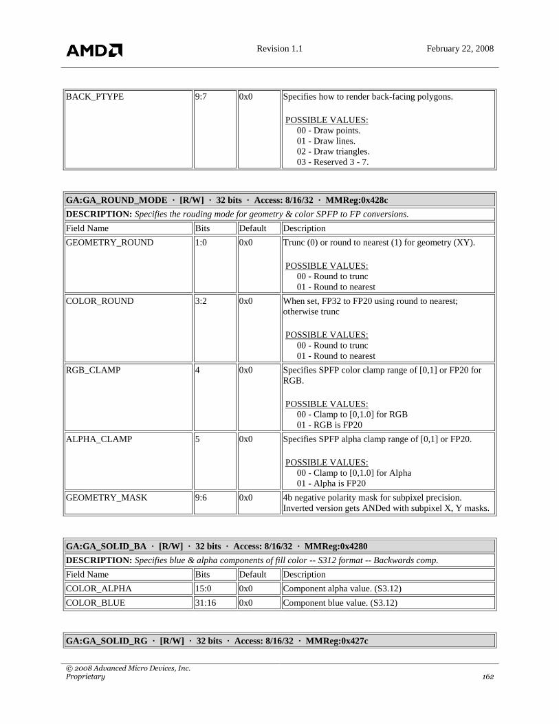
Revision 1.1 February 22, 2008
© 2008 Advanced Micro Devices, Inc. Proprietary 162
BACK_PTYPE 9:7 0x0 Specifies how to render back-facing polygons.
POSSIBLE VALUES:
00 - Draw points.
01 - Draw lines.
02 - Draw triangles.
03 - Reserved 3 - 7.
GA:GA_ROUND_MODE · [R/W] · 32 bits · Access: 8/16/32 · MMReg:0x428c
DESCRIPTION: Specifies the rouding mode for geometry & color SPFP to FP conversions.
Field Name Bits Default Description
GEOMETRY_ROUND 1:0 0x0 Trunc (0) or round to nearest (1) for geometry (XY).
POSSIBLE VALUES:
00 - Round to trunc
01 - Round to nearest
COLOR_ROUND 3:2 0x0 When set, FP32 to FP20 using round to nearest;
otherwise trunc
POSSIBLE VALUES:
00 - Round to trunc
01 - Round to nearest
RGB_CLAMP 4 0x0 Specifies SPFP color clamp range of [0,1] or FP20 for
RGB.
POSSIBLE VALUES:
00 - Clamp to [0,1.0] for RGB
01 - RGB is FP20
ALPHA_CLAMP 5 0x0 Specifies SPFP alpha clamp range of [0,1] or FP20.
POSSIBLE VALUES:
00 - Clamp to [0,1.0] for Alpha
01 - Alpha is FP20
GEOMETRY_MASK 9:6 0x0 4b negative polarity mask for subpixel precision.
Inverted version gets ANDed with subpixel X, Y masks.
GA:GA_SOLID_BA · [R/W] · 32 bits · Access: 8/16/32 · MMReg:0x4280
DESCRIPTION: Specifies blue & alpha components of fill color -- S312 format -- Backwards comp.
Field Name Bits Default Description
COLOR_ALPHA 15:0 0x0 Component alpha value. (S3.12)
COLOR_BLUE 31:16 0x0 Component blue value. (S3.12)
GA:GA_SOLID_RG · [R/W] · 32 bits · Access: 8/16/32 · MMReg:0x427c

Revision 1.1 February 22, 2008
© 2008 Advanced Micro Devices, Inc. Proprietary 163
DESCRIPTION: Specifies red & green components of fill color -- S312 format -- Backwards comp.
Field Name Bits Default Description
COLOR_GREEN 15:0 0x0 Component green value (S3.12).
COLOR_RED 31:16 0x0 Component red value (S3.12).
GA:GA_TRIANGLE_STIPPLE · [R/W] · 32 bits · Access: 8/16/32 · MMReg:0x4214
DESCRIPTION: Specifies amount to shift integer position of vertex (screen space) before converting to float for
triangle stipple.
Field Name Bits Default Description
X_SHIFT 3:0 0x0 Amount to shift x position before conversion to SPFP.
Y_SHIFT 19:16 0x0 Amount to shift y position before conversion to SPFP.
GA:GA_US_VECTOR_DATA · [R/W] · 32 bits · Access: 8/16/32 · MMReg:0x4254
DESCRIPTION: Data register for loading US instructions and constants
Field Name Bits Default Description
DATA 31:0 0x0 32 bit dword
GA:GA_US_VECTOR_INDEX · [R/W] · 32 bits · Access: 8/16/32 · MMReg:0x4250
DESCRIPTION: Used to load US instructions and constants
Field Name Bits Default Description
INDEX 8:0 0x0 Instruction (TYPE == GA_US_VECTOR_INST) or
constant (TYPE == GA_US_VECTOR_CONST)
number at which to start loading. The GA will then
expect n*6 (instructions) or n*4 (constants) writes to
GA_US_VECTOR_DATA. The GA will self-increment
until this register is written again. For instructions, the
GA expects the dwords in the following order:
US_CMN_INST, US_ALU_RGB_ADDR,
US_ALU_ALPHA_ADDR, US_ALU_ALPHA,
US_RGB_INST, US_ALPHA_INST, US_RGBA_INST.
For constants, the GA expects the dwords in RGBA
order.
TYPE 16 0x0 Specifies if the GA should load instructions or constants.
POSSIBLE VALUES:
00 - Load instructions - INDEX is an instruction
index
01 - Load constants - INDEX is a constant index
CLAMP 17 0x0 POSSIBLE VALUES:
00 - No clamping of data - Default
01 - Clamp to [-1.0,1.0] constant data
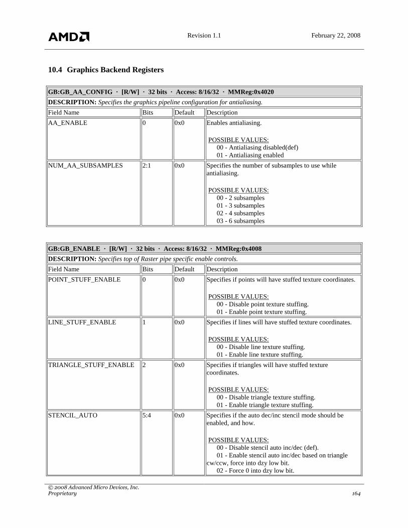
Revision 1.1 February 22, 2008
© 2008 Advanced Micro Devices, Inc. Proprietary 164
10.4 Graphics Backend Registers
GB:GB_AA_CONFIG · [R/W] · 32 bits · Access: 8/16/32 · MMReg:0x4020
DESCRIPTION: Specifies the graphics pipeline configuration for antialiasing.
Field Name Bits Default Description
AA_ENABLE 0 0x0 Enables antialiasing.
POSSIBLE VALUES:
00 - Antialiasing disabled(def)
01 - Antialiasing enabled
NUM_AA_SUBSAMPLES 2:1 0x0 Specifies the number of subsamples to use while
antialiasing.
POSSIBLE VALUES:
00 - 2 subsamples
01 - 3 subsamples
02 - 4 subsamples
03 - 6 subsamples
GB:GB_ENABLE · [R/W] · 32 bits · Access: 8/16/32 · MMReg:0x4008
DESCRIPTION: Specifies top of Raster pipe specific enable controls.
Field Name Bits Default Description
POINT_STUFF_ENABLE 0 0x0 Specifies if points will have stuffed texture coordinates.
POSSIBLE VALUES:
00 - Disable point texture stuffing.
01 - Enable point texture stuffing.
LINE_STUFF_ENABLE 1 0x0 Specifies if lines will have stuffed texture coordinates.
POSSIBLE VALUES:
00 - Disable line texture stuffing.
01 - Enable line texture stuffing.
TRIANGLE_STUFF_ENABLE 2 0x0 Specifies if triangles will have stuffed texture
coordinates.
POSSIBLE VALUES:
00 - Disable triangle texture stuffing.
01 - Enable triangle texture stuffing.
STENCIL_AUTO 5:4 0x0 Specifies if the auto dec/inc stencil mode should be
enabled, and how.
POSSIBLE VALUES:
00 - Disable stencil auto inc/dec (def).
01 - Enable stencil auto inc/dec based on triangle
cw/ccw, force into dzy low bit.
02 - Force 0 into dzy low bit.
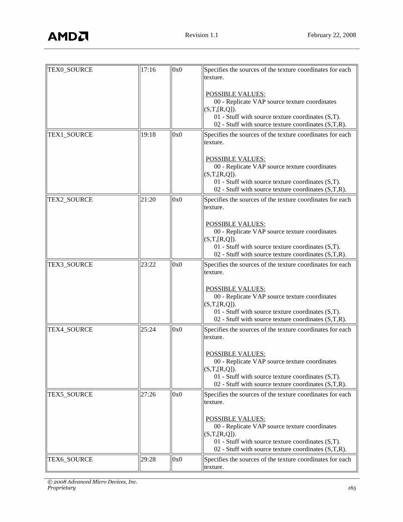
Revision 1.1 February 22, 2008
© 2008 Advanced Micro Devices, Inc. Proprietary 165
TEX0_SOURCE 17:16 0x0 Specifies the sources of the texture coordinates for each
texture.
POSSIBLE VALUES:
00 - Replicate VAP source texture coordinates
(S,T,[R,Q]).
01 - Stuff with source texture coordinates (S,T).
02 - Stuff with source texture coordinates (S,T,R).
TEX1_SOURCE 19:18 0x0 Specifies the sources of the texture coordinates for each
texture.
POSSIBLE VALUES:
00 - Replicate VAP source texture coordinates
(S,T,[R,Q]).
01 - Stuff with source texture coordinates (S,T).
02 - Stuff with source texture coordinates (S,T,R).
TEX2_SOURCE 21:20 0x0 Specifies the sources of the texture coordinates for each
texture.
POSSIBLE VALUES:
00 - Replicate VAP source texture coordinates
(S,T,[R,Q]).
01 - Stuff with source texture coordinates (S,T).
02 - Stuff with source texture coordinates (S,T,R).
TEX3_SOURCE 23:22 0x0 Specifies the sources of the texture coordinates for each
texture.
POSSIBLE VALUES:
00 - Replicate VAP source texture coordinates
(S,T,[R,Q]).
01 - Stuff with source texture coordinates (S,T).
02 - Stuff with source texture coordinates (S,T,R).
TEX4_SOURCE 25:24 0x0 Specifies the sources of the texture coordinates for each
texture.
POSSIBLE VALUES:
00 - Replicate VAP source texture coordinates
(S,T,[R,Q]).
01 - Stuff with source texture coordinates (S,T).
02 - Stuff with source texture coordinates (S,T,R).
TEX5_SOURCE 27:26 0x0 Specifies the sources of the texture coordinates for each
texture.
POSSIBLE VALUES:
00 - Replicate VAP source texture coordinates
(S,T,[R,Q]).
01 - Stuff with source texture coordinates (S,T).
02 - Stuff with source texture coordinates (S,T,R).
TEX6_SOURCE 29:28 0x0 Specifies the sources of the texture coordinates for each
texture.

Revision 1.1 February 22, 2008
© 2008 Advanced Micro Devices, Inc. Proprietary 166
POSSIBLE VALUES:
00 - Replicate VAP source texture coordinates
(S,T,[R,Q]).
01 - Stuff with source texture coordinates (S,T).
02 - Stuff with source texture coordinates (S,T,R).
TEX7_SOURCE 31:30 0x0 Specifies the sources of the texture coordinates for each
texture.
POSSIBLE VALUES:
00 - Replicate VAP source texture coordinates
(S,T,[R,Q]).
01 - Stuff with source texture coordinates (S,T).
02 - Stuff with source texture coordinates (S,T,R).
GB:GB_FIFO_SIZE · [R/W] · 32 bits · Access: 8/16/32 · MMReg:0x4024
DESCRIPTION: Specifies the sizes of the various FIFO`s in the sc/rs/us. This register must be the first one written
Field Name Bits Default Description
SC_IFIFO_SIZE 1:0 0x0 Size of scan converter input FIFO (XYZ)
POSSIBLE VALUES:
00 - 32 words
01 - 64 words
02 - 128 words
03 - 256 words
SC_TZFIFO_SIZE 3:2 0x0 Size of scan converter top-of-pipe Z FIFO
POSSIBLE VALUES:
00 - 16 words
01 - 32 words
02 - 64 words
03 - 128 words
SC_BFIFO_SIZE 5:4 0x0 Size of scan converter input FIFO (B)
POSSIBLE VALUES:
00 - 32 words
01 - 64 words
02 - 128 words
03 - 256 words
RS_TFIFO_SIZE 7:6 0x0 Size of ras input FIFO (Texture)
POSSIBLE VALUES:
00 - 64 words
01 - 128 words
02 - 256 words
03 - 512 words
RS_CFIFO_SIZE 9:8 0x0 Size of ras input FIFO (Color)

Revision 1.1 February 22, 2008
© 2008 Advanced Micro Devices, Inc. Proprietary 167
POSSIBLE VALUES:
00 - 64 words
01 - 128 words
02 - 256 words
03 - 512 words
US_RAM_SIZE 11:10 0x0 Size of us RAM
POSSIBLE VALUES:
00 - 64 words
01 - 128 words
02 - 256 words
03 - 512 words
US_OFIFO_SIZE 13:12 0x0 Size of us output FIFO (RGBA)
POSSIBLE VALUES:
00 - 16 words
01 - 32 words
02 - 64 words
03 - 128 words
US_WFIFO_SIZE 15:14 0x0 Size of us output FIFO (W)
POSSIBLE VALUES:
00 - 16 words
01 - 32 words
02 - 64 words
03 - 128 words
RS_HIGHWATER_COL 18:16 0x0 High water mark for RS colors` fifo -- NOT USED
RS_HIGHWATER_TEX 21:19 0x0 High water mark for RS textures` fifo -- NOT USED
US_OFIFO_HIGHWATER 23:22 0x0 High water mark for US output fifo
POSSIBLE VALUES:
00 - 0 words
01 - 4 words
02 - 8 words
03 - 12 words
US_CUBE_FIFO_HIGHWATER 28:24 0x0 High water mark for US cube map fifo
GB:GB_FIFO_SIZE1 · [R/W] · 32 bits · Access: 8/16/32 · MMReg:0x4070
DESCRIPTION: Specifies the sizes of the various FIFO`s in the sc/rs.
Field Name Bits Default Description
SC_HIGHWATER_IFIFO 5:0 0x0 High water mark for SC input fifo
SC_HIGHWATER_BFIFO 11:6 0x0 High water mark for SC input fifo (B)
RS_HIGHWATER_COL 17:12 0x0 High water mark for RS colors` fifo
RS_HIGHWATER_TEX 23:18 0x0 High water mark for RS textures` fifo

Revision 1.1 February 22, 2008
© 2008 Advanced Micro Devices, Inc. Proprietary 168
GB:GB_MSPOS0 · [R/W] · 32 bits · Access: 8/16/32 · MMReg:0x4010
DESCRIPTION: Specifies the position of multisamples 0 through 2
Field Name Bits Default Description
MS_X0 3:0 0x0 Specifies the x and y position (in subpixels) of
multisample 0
MS_Y0 7:4 0x0 Specifies the x and y position (in subpixels) of
multisample 0
MS_X1 11:8 0x0 Specifies the x and y position (in subpixels) of
multisample 1
MS_Y1 15:12 0x0 Specifies the x and y position (in subpixels) of
multisample 1
MS_X2 19:16 0x0 Specifies the x and y position (in subpixels) of
multisample 2
MS_Y2 23:20 0x0 Specifies the x and y position (in subpixels) of
multisample 2
MSBD0_Y 27:24 0x0 Specifies the minimum x and y distance (in subpixels)
between the pixel edge and the multisamples. These
values are used in the first (coarse) scan converter
MSBD0_X 31:28 0x0 Specifies the minimum x and y distance (in subpixels)
between the pixel edge and the multisamples. These
values are used in the first (coarse) scan converter
GB:GB_MSPOS1 · [R/W] · 32 bits · Access: 8/16/32 · MMReg:0x4014
DESCRIPTION: Specifies the position of multisamples 3 through 5
Field Name Bits Default Description
MS_X3 3:0 0x0 Specifies the x and y position (in subpixels) of
multisample 3
MS_Y3 7:4 0x0 Specifies the x and y position (in subpixels) of
multisample 3
MS_X4 11:8 0x0 Specifies the x and y position (in subpixels) of
multisample 4
MS_Y4 15:12 0x0 Specifies the x and y position (in subpixels) of
multisample 4
MS_X5 19:16 0x0 Specifies the x and y position (in subpixels) of
multisample 5
MS_Y5 23:20 0x0 Specifies the x and y position (in subpixels) of
multisample 5
MSBD1 27:24 0x0 Specifies the minimum distance (in subpixels) between
the pixel edge and the multisamples. This value is used
in the second (quad) scan converter
GB:GB_PIPE_SELECT · [R/W] · 32 bits · Access: 8/16/32 · MMReg:0x402c
DESCRIPTION: Selects which of 4 pipes are active.

Revision 1.1 February 22, 2008
© 2008 Advanced Micro Devices, Inc. Proprietary 169
Field Name Bits Default Description
PIPE0_ID 1:0 0x0 Maps physical pipe 0 to logical pipe ID (def 0).
PIPE1_ID 3:2 0x1 Maps physical pipe 1 to logical pipe ID (def 1).
PIPE2_ID 5:4 0x2 Maps physical pipe 2 to logical pipe ID (def 2).
PIPE3_ID 7:6 0x3 Maps physical pipe 3 to logical pipe ID (def 3).
PIPE_MASK 11:8 0x0 4b mask, indicates which physical pipes are enabled (def
none=0x0) -- B3=P3, B2=P2, B1=P1, B0=P0. -- 1:
enabled, 0: disabled
MAX_PIPE 13:12 0x3 2b, indicates, by the fuses, the max number of allowed
pipes. 0 = 1 pipe ... 3 = 4 pipes -- Read Only
BAD_PIPES 17:14 0xF 4b, indicates, by the fuses, the bad pipes: B3=P3, B2=P2,
B1=P1, B0=P0 -- 1: bad, 0: good -- Read Only
CONFIG_PIPES 18 0x0 If this bit is set when writing this register, the logical
pipe ID values are assigned automatically based on the
values that are read back in the MAX_PIPE and
BAD_PIPES fields. This field is always read back as 0.
POSSIBLE VALUES:
00 - Do nothing
01 - Force self-configuration
GB:GB_SELECT · [R/W] · 32 bits · Access: 8/16/32 · MMReg:0x401c
DESCRIPTION: Specifies various polygon specific selects (fog, depth, perspective).
Field Name Bits Default Description
FOG_SELECT 2:0 0x0 Specifies source for outgoing (GA to SU) fog value.
POSSIBLE VALUES:
00 - Select C0A
01 - Select C1A
02 - Select C2A
03 - Select C3A
04 - Select 1/(1/W)
05 - Select Z
DEPTH_SELECT 3 0x0 Specifies source for outgoing (GA/SU & SU/RAS) depth
value.
POSSIBLE VALUES:
00 - Select Z
01 - Select 1/(1/W)
W_SELECT 4 0x0 Specifies source for outgoing (1/W) value, used to
disable perspective correct colors/textures.
POSSIBLE VALUES:
00 - Select (1/W)
01 - Select 1.0
FOG_STUFF_ENABLE 5 0x0 Controls enabling of fog stuffing into texture coordinate.
Revision 1.1 February 22, 2008
© 2008 Advanced Micro Devices, Inc. Proprietary 170
POSSIBLE VALUES:
00 - Disable fog texture stuffing
01 - Enable fog texture stuffing
FOG_STUFF_TEX 9:6 0x0 Controls which texture gets fog value
FOG_STUFF_COMP 11:10 0x0 Controls which component of texture gets fog value
GB:GB_TILE_CONFIG · [R/W] · 32 bits · Access: 8/16/32 · MMReg:0x4018
DESCRIPTION: Specifies the graphics pipeline configuration for rasterization
Field Name Bits Default Description
ENABLE 0 0x1 Enables tiling, otherwise all tiles receive all polygons.
POSSIBLE VALUES:
00 - Tiling disabled.
01 - Tiling enabled (def).
PIPE_COUNT 3:1 0x0 Specifies the number of active pipes and contexts (up to
4 pipes, 1 ctx). When this field is written, it is
automatically reduced by hardware so as not to use more
pipes than the number indicated in
GB_PIPE_SELECT.MAX_PIPES or the number of
pipes left unmasked GB_PIPE_SELECT.BAD_PIPES.
The potentially altered value is read back, rather than the
original value written by software.
POSSIBLE VALUES:
00 - RV350 (1 pipe, 1 ctx)
03 - R300 (2 pipes, 1 ctx)
06 – R420-3P (3 pipes, 1 ctx)
07 – R420 (4 pipes, 1 ctx)
TILE_SIZE 5:4 0x1 Specifies width & height (square), in pixels (only 16, 32
available).
POSSIBLE VALUES:
00 - 8 pixels.
01 - 16 pixels.
02 - 32 pixels.
SUPER_SIZE 8:6 0x0 Specifies number of tiles and config in super chip
configuration.
POSSIBLE VALUES:
00 - 1x1 tile (one 1x1).
01 - 2 tiles (two 1x1 : ST-A,B).
02 - 4 tiles (one 2x2).
03 - 8 tiles (two 2x2 : ST-A,B).
04 - 16 tiles (one 4x4).
05 - 32 tiles (two 4x4 : ST-A,B).
06 - 64 tiles (one 8x8).
07 - 128 tiles (two 8x8 : ST-A,B).

Revision 1.1 February 22, 2008
© 2008 Advanced Micro Devices, Inc. Proprietary 171
SUPER_X 11:9 0x0 X Location of chip within super tile.
SUPER_Y 14:12 0x0 Y Location of chip within super tile.
SUPER_TILE 15 0x0 Tile location of chip in a multi super tile config (Super
size of 2,8,32 or 128).
POSSIBLE VALUES:
00 - ST-A tile.
01 - ST-B tile.
SUBPIXEL 16 0x0 Specifies the precision of subpixels wrt pixels (12 or 16).
POSSIBLE VALUES:
00 - Select 1/12 subpixel precision.
01 - Select 1/16 subpixel precision.
QUADS_PER_RAS 18:17 0x0 Specifies the number of quads to be sent to each
rasterizer in turn when in RV300B or R300B mode
POSSIBLE VALUES:
00 - 4 Quads
01 - 8 Quads
02 - 16 Quads
03 - 32 Quads
BB_SCAN 19 0x0 Specifies whether to use an intercept or bounding box
based calculation for the first (coarse) scan converter
POSSIBLE VALUES:
00 - Use intercept based scan converter
01 - Use bounding box based scan converter
ALT_SCAN_EN 20 0x0 Specifies whether to use an altenate scan pattern for the
coarse scan converter
POSSIBLE VALUES:
00 - Use normal left-right scan
01 - Use alternate left-right-left scan
ALT_OFFSET 21 0x0 Not used -- should be 0
POSSIBLE VALUES:
00 - Not used
01 - Not used
SUBPRECISION 22 0x0 Set to 0
ALT_TILING 23 0x0 Support for 3x2 tiling in 3P mode
POSSIBLE VALUES:
00 - Use default tiling in all tiling modes
01 - Use alternative 3x2 tiling in 3P mode
Z_EXTENDED 24 0x0 Support for extended setup Z range from [0,1] to [-2,2]
with per pixel clamping
POSSIBLE VALUES:
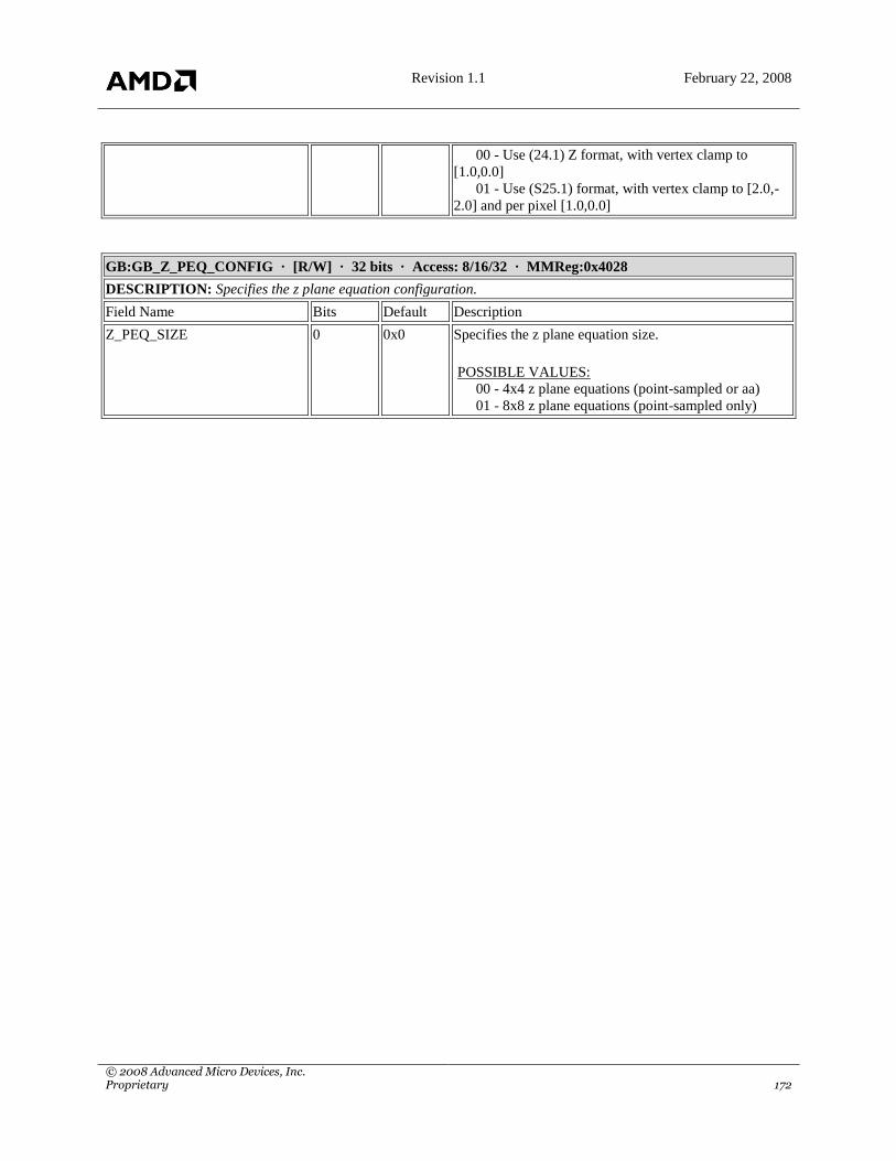
Revision 1.1 February 22, 2008
© 2008 Advanced Micro Devices, Inc. Proprietary 172
00 - Use (24.1) Z format, with vertex clamp to
[1.0,0.0]
01 - Use (S25.1) format, with vertex clamp to [2.0,-
2.0] and per pixel [1.0,0.0]
GB:GB_Z_PEQ_CONFIG · [R/W] · 32 bits · Access: 8/16/32 · MMReg:0x4028
DESCRIPTION: Specifies the z plane equation configuration.
Field Name Bits Default Description
Z_PEQ_SIZE 0 0x0 Specifies the z plane equation size.
POSSIBLE VALUES:
00 - 4x4 z plane equations (point-sampled or aa)
01 - 8x8 z plane equations (point-sampled only)

Revision 1.1 February 22, 2008
© 2008 Advanced Micro Devices, Inc. Proprietary 173
10.5 Rasterizer Registers
RS:RS_COUNT · [R/W] · 32 bits · Access: 8/16/32 · MMReg:0x4300
DESCRIPTION: This register specifies the rasterizer input packet configuration
Field Name Bits Default Description
IT_COUNT 6:0 0x0 Specifies the total number of texture address components
contained in the rasterizer input packet (0:32).
IC_COUNT 10:7 0x0 Specifies the total number of colors contained in the
rasterizer input packet (0:4).
W_ADDR 17:12 0x0 Specifies the relative rasterizer input packet location of w
(if w_count==1)
HIRES_EN 18 0x0 Enable high resolution texture coordinate output when q
is equal to 1
RS:RS_INST_[0-15] · [R/W] · 32 bits · Access: 8/16/32 · MMReg:0x4320-0x435c
DESCRIPTION: This table specifies what happens during each rasterizer instruction
Field Name Bits Default Description
TEX_ID 3:0 0x0 Specifies the index (into the RS_IP table) of the texture
address output during this rasterizer instruction
TEX_CN 4 0x0 Write enable for texture address
POSSIBLE VALUES:
00 - No write - texture coordinate not valid
01 - write - texture valid
TEX_ADDR 11:5 0x0 Specifies the destination address (within the current pixel
stack frame) of the texture address output during this
rasterizer instruction
COL_ID 15:12 0x0 Specifies the index (into the RS_IP table) of the color
output during this rasterizer instruction
COL_CN 17:16 0x0 Write enable for color
POSSIBLE VALUES:
00 - No write - color not valid
01 - write - color valid
02 - write fbuffer - XY00->RGBA
03 - write backface - B000->RGBA
COL_ADDR 24:18 0x0 Specifies the destination address (within the current pixel
stack frame) of the color output during this rasterizer
instruction
TEX_ADJ 25 0x0 Specifies whether to sample texture coordinates at the
real or adjusted pixel centers
POSSIBLE VALUES:
00 - Sample texture coordinates at real pixel centers
01 - Sample texture coordinates at adjusted pixel
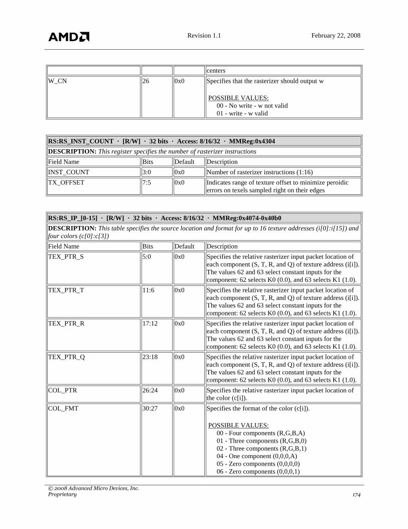
Revision 1.1 February 22, 2008
© 2008 Advanced Micro Devices, Inc. Proprietary 174
centers
W_CN 26 0x0 Specifies that the rasterizer should output w
POSSIBLE VALUES:
00 - No write - w not valid
01 - write - w valid
RS:RS_INST_COUNT · [R/W] · 32 bits · Access: 8/16/32 · MMReg:0x4304
DESCRIPTION: This register specifies the number of rasterizer instructions
Field Name Bits Default Description
INST_COUNT 3:0 0x0 Number of rasterizer instructions (1:16)
TX_OFFSET 7:5 0x0 Indicates range of texture offset to minimize peroidic
errors on texels sampled right on their edges
RS:RS_IP_[0-15] · [R/W] · 32 bits · Access: 8/16/32 · MMReg:0x4074-0x40b0
DESCRIPTION: This table specifies the source location and format for up to 16 texture addresses (i[0]:i[15]) and
four colors (c[0]:c[3])
Field Name Bits Default Description
TEX_PTR_S 5:0 0x0 Specifies the relative rasterizer input packet location of
each component (S, T, R, and Q) of texture address (i[i]).
The values 62 and 63 select constant inputs for the
component: 62 selects K0 (0.0), and 63 selects K1 (1.0).
TEX_PTR_T 11:6 0x0 Specifies the relative rasterizer input packet location of
each component (S, T, R, and Q) of texture address (i[i]).
The values 62 and 63 select constant inputs for the
component: 62 selects K0 (0.0), and 63 selects K1 (1.0).
TEX_PTR_R 17:12 0x0 Specifies the relative rasterizer input packet location of
each component (S, T, R, and Q) of texture address (i[i]).
The values 62 and 63 select constant inputs for the
component: 62 selects K0 (0.0), and 63 selects K1 (1.0).
TEX_PTR_Q 23:18 0x0 Specifies the relative rasterizer input packet location of
each component (S, T, R, and Q) of texture address (i[i]).
The values 62 and 63 select constant inputs for the
component: 62 selects K0 (0.0), and 63 selects K1 (1.0).
COL_PTR 26:24 0x0 Specifies the relative rasterizer input packet location of
the color (c[i]).
COL_FMT 30:27 0x0 Specifies the format of the color (c[i]).
POSSIBLE VALUES:
00 - Four components (R,G,B,A)
01 - Three components (R,G,B,0)
02 - Three components (R,G,B,1)
04 - One component (0,0,0,A)
05 - Zero components (0,0,0,0)
06 - Zero components (0,0,0,1)

Revision 1.1 February 22, 2008
© 2008 Advanced Micro Devices, Inc. Proprietary 175
08 - One component (1,1,1,A)
09 - Zero components (1,1,1,0)
10 - Zero components (1,1,1,1)
OFFSET_EN 31 0x0 Enable application of the TX_OFFSET in
RS_INST_COUNT
POSSIBLE VALUES:
00 - Do not apply the TX_OFFSET in
RS_INST_COUNT
01 - Apply the TX_OFFSET specified by
RS_INST_COUNT
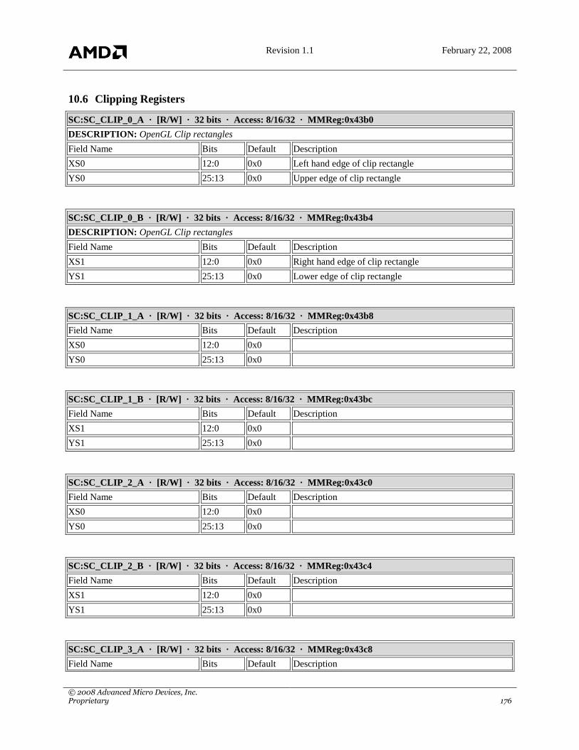
Revision 1.1 February 22, 2008
© 2008 Advanced Micro Devices, Inc. Proprietary 176
10.6 Clipping Registers
SC:SC_CLIP_0_A · [R/W] · 32 bits · Access: 8/16/32 · MMReg:0x43b0
DESCRIPTION: OpenGL Clip rectangles
Field Name Bits Default Description
XS0 12:0 0x0 Left hand edge of clip rectangle
YS0 25:13 0x0 Upper edge of clip rectangle
SC:SC_CLIP_0_B · [R/W] · 32 bits · Access: 8/16/32 · MMReg:0x43b4
DESCRIPTION: OpenGL Clip rectangles
Field Name Bits Default Description
XS1 12:0 0x0 Right hand edge of clip rectangle
YS1 25:13 0x0 Lower edge of clip rectangle
SC:SC_CLIP_1_A · [R/W] · 32 bits · Access: 8/16/32 · MMReg:0x43b8
Field Name Bits Default Description
XS0 12:0 0x0
YS0 25:13 0x0
SC:SC_CLIP_1_B · [R/W] · 32 bits · Access: 8/16/32 · MMReg:0x43bc
Field Name Bits Default Description
XS1 12:0 0x0
YS1 25:13 0x0
SC:SC_CLIP_2_A · [R/W] · 32 bits · Access: 8/16/32 · MMReg:0x43c0
Field Name Bits Default Description
XS0 12:0 0x0
YS0 25:13 0x0
SC:SC_CLIP_2_B · [R/W] · 32 bits · Access: 8/16/32 · MMReg:0x43c4
Field Name Bits Default Description
XS1 12:0 0x0
YS1 25:13 0x0
SC:SC_CLIP_3_A · [R/W] · 32 bits · Access: 8/16/32 · MMReg:0x43c8
Field Name Bits Default Description

Revision 1.1 February 22, 2008
© 2008 Advanced Micro Devices, Inc. Proprietary 177
XS0 12:0 0x0
YS0 25:13 0x0
SC:SC_CLIP_3_B · [R/W] · 32 bits · Access: 8/16/32 · MMReg:0x43cc
Field Name Bits Default Description
XS1 12:0 0x0
YS1 25:13 0x0
SC:SC_CLIP_RULE · [R/W] · 32 bits · Access: 8/16/32 · MMReg:0x43d0
DESCRIPTION: OpenGL Clip boolean function
Field Name Bits Default Description
CLIP_RULE 15:0 0x0 OpenGL Clip boolean function. The `inside` flags for
each of the four clip rectangles form a 4-bit binary
number. The corresponding bit in this 16-bit number
specifies whether the pixel is visible.
SC:SC_EDGERULE · [R/W] · 32 bits · Access: 8/16/32 · MMReg:0x43a8
DESCRIPTION: Edge rules - what happens when an edge falls exactly on a sample point
Field Name Bits Default Description
ER_TRI 4:0 0x0 Edge rules for triangles, points, left-right lines, right-left
lines, upper-bottom lines, bottom-upper lines. For values
0 to 15, bit 0 specifies whether a sample on a horizontal-
bottom edge is in, bit 1 specifies whether a sample on a
horizontal-top edge is in, bit 2 species whether a sample
on a right edge is in, bit 3 specifies whether a sample on
a left edge is in. For values 16 to 31, bit 0 specifies
whether a sample on a vertical-right edge is in, bit 1
specifies whether a sample on a vertical-left edge is in,
bit 2 species whether a sample on a bottom edge is in, bit
3 specifies whether a sample on a top edge is in
POSSIBLE VALUES:
00 - L-in,R-in,HT-in,HB-in
01 - L-in,R-in,HT-in,HB-out
02 - L-in,R-in,HT-out,HB-in
03 - L-in,R-in,HT-out,HB-out
04 - L-in,R-out,HT-in,HB-in
05 - L-in,R-out,HT-in,HB-out
06 - L-in,R-out,HT-out,HB-in
07 - L-in,R-out,HT-out,HB-out
08 - L-out,R-in,HT-in,HB-in
09 - L-out,R-in,HT-in,HB-out
10 - L-out,R-in,HT-out,HB-in
11 - L-out,R-in,HT-out,HB-out
12 - L-out,R-out,HT-in,HB-in

Revision 1.1 February 22, 2008
© 2008 Advanced Micro Devices, Inc. Proprietary 178
13 - L-out,R-out,HT-in,HB-out
14 - L-out,R-out,HT-out,HB-in
15 - L-out,R-out,HT-out,HB-out
16 - T-in,B-in,VL-in,VR-in
17 - T-in,B-in,VL-in,VR-out
18 - T-in,B-in,VL,VR-in
19 - T-in,B-in,VL-out,VR-out
20 - T-out,B-in,VL-in,VR-in
21 - T-out,B-in,VL-in,VR-out
22 - T-out,B-in,VL-out,VR-in
23 - T-out,B-in,VL-out,VR-out
24 - T-in,B-out,VL-in,VR-in
25 - T-in,B-out,VL-in,VR-out
26 - T-in,B-out,VL-out,VR-in
27 - T-in,B-out,VL-out,VR-out
28 - T-out,B-out,VL-in,VR-in
29 - T-out,B-out,VL-in,VR-out
30 - T-out,B-out,VL-out,VR-in
31 - T-out,B-out,VL-out,VR-out
ER_POINT 9:5 0x0 Edge rules for triangles, points, left-right lines, right-left
lines, upper-bottom lines, bottom-upper lines. For values
0 to 15, bit 0 specifies whether a sample on a horizontal-
bottom edge is in, bit 1 specifies whether a sample on a
horizontal-top edge is in, bit 2 species whether a sample
on a right edge is in, bit 3 specifies whether a sample on
a left edge is in. For values 16 to 31, bit 0 specifies
whether a sample on a vertical-right edge is in, bit 1
specifies whether a sample on a vertical-left edge is in,
bit 2 species whether a sample on a bottom edge is in, bit
3 specifies whether a sample on a top edge is in
POSSIBLE VALUES:
00 - L-in,R-in,HT-in,HB-in
01 - L-in,R-in,HT-in,HB-out
02 - L-in,R-in,HT-out,HB-in
03 - L-in,R-in,HT-out,HB-out
04 - L-in,R-out,HT-in,HB-in
05 - L-in,R-out,HT-in,HB-out
06 - L-in,R-out,HT-out,HB-in
07 - L-in,R-out,HT-out,HB-out
08 - L-out,R-in,HT-in,HB-in
09 - L-out,R-in,HT-in,HB-out
10 - L-out,R-in,HT-out,HB-in
11 - L-out,R-in,HT-out,HB-out
12 - L-out,R-out,HT-in,HB-in
13 - L-out,R-out,HT-in,HB-out
14 - L-out,R-out,HT-out,HB-in
15 - L-out,R-out,HT-out,HB-out
16 - T-in,B-in,VL-in,VR-in
17 - T-in,B-in,VL-in,VR-out
18 - T-in,B-in,VL,VR-in
19 - T-in,B-in,VL-out,VR-out
20 - T-out,B-in,VL-in,VR-in
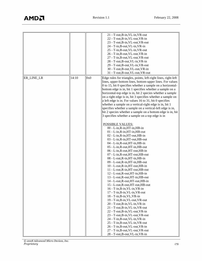
Revision 1.1 February 22, 2008
© 2008 Advanced Micro Devices, Inc. Proprietary 179
21 - T-out,B-in,VL-in,VR-out
22 - T-out,B-in,VL-out,VR-in
23 - T-out,B-in,VL-out,VR-out
24 - T-in,B-out,VL-in,VR-in
25 - T-in,B-out,VL-in,VR-out
26 - T-in,B-out,VL-out,VR-in
27 - T-in,B-out,VL-out,VR-out
28 - T-out,B-out,VL-in,VR-in
29 - T-out,B-out,VL-in,VR-out
30 - T-out,B-out,VL-out,VR-in
31 - T-out,B-out,VL-out,VR-out
ER_LINE_LR 14:10 0x0 Edge rules for triangles, points, left-right lines, right-left
lines, upper-bottom lines, bottom-upper lines. For values
0 to 15, bit 0 specifies whether a sample on a horizontal-
bottom edge is in, bit 1 specifies whether a sample on a
horizontal-top edge is in, bit 2 species whether a sample
on a right edge is in, bit 3 specifies whether a sample on
a left edge is in. For values 16 to 31, bit 0 specifies
whether a sample on a vertical-right edge is in, bit 1
specifies whether a sample on a vertical-left edge is in,
bit 2 species whether a sample on a bottom edge is in, bit
3 specifies whether a sample on a top edge is in
POSSIBLE VALUES:
00 - L-in,R-in,HT-in,HB-in
01 - L-in,R-in,HT-in,HB-out
02 - L-in,R-in,HT-out,HB-in
03 - L-in,R-in,HT-out,HB-out
04 - L-in,R-out,HT-in,HB-in
05 - L-in,R-out,HT-in,HB-out
06 - L-in,R-out,HT-out,HB-in
07 - L-in,R-out,HT-out,HB-out
08 - L-out,R-in,HT-in,HB-in
09 - L-out,R-in,HT-in,HB-out
10 - L-out,R-in,HT-out,HB-in
11 - L-out,R-in,HT-out,HB-out
12 - L-out,R-out,HT-in,HB-in
13 - L-out,R-out,HT-in,HB-out
14 - L-out,R-out,HT-out,HB-in
15 - L-out,R-out,HT-out,HB-out
16 - T-in,B-in,VL-in,VR-in
17 - T-in,B-in,VL-in,VR-out
18 - T-in,B-in,VL,VR-in
19 - T-in,B-in,VL-out,VR-out
20 - T-out,B-in,VL-in,VR-in
21 - T-out,B-in,VL-in,VR-out
22 - T-out,B-in,VL-out,VR-in
23 - T-out,B-in,VL-out,VR-out
24 - T-in,B-out,VL-in,VR-in
25 - T-in,B-out,VL-in,VR-out
26 - T-in,B-out,VL-out,VR-in
27 - T-in,B-out,VL-out,VR-out
28 - T-out,B-out,VL-in,VR-in

Revision 1.1 February 22, 2008
© 2008 Advanced Micro Devices, Inc. Proprietary 180
29 - T-out,B-out,VL-in,VR-out
30 - T-out,B-out,VL-out,VR-in
31 - T-out,B-out,VL-out,VR-out
ER_LINE_RL 19:15 0x0 Edge rules for triangles, points, left-right lines, right-left
lines, upper-bottom lines, bottom-upper lines. For values
0 to 15, bit 0 specifies whether a sample on a horizontal-
bottom edge is in, bit 1 specifies whether a sample on a
horizontal-top edge is in, bit 2 species whether a sample
on a right edge is in, bit 3 specifies whether a sample on
a left edge is in. For values 16 to 31, bit 0 specifies
whether a sample on a vertical-right edge is in, bit 1
specifies whether a sample on a vertical-left edge is in,
bit 2 species whether a sample on a bottom edge is in, bit
3 specifies whether a sample on a top edge is in
POSSIBLE VALUES:
00 - L-in,R-in,HT-in,HB-in
01 - L-in,R-in,HT-in,HB-out
02 - L-in,R-in,HT-out,HB-in
03 - L-in,R-in,HT-out,HB-out
04 - L-in,R-out,HT-in,HB-in
05 - L-in,R-out,HT-in,HB-out
06 - L-in,R-out,HT-out,HB-in
07 - L-in,R-out,HT-out,HB-out
08 - L-out,R-in,HT-in,HB-in
09 - L-out,R-in,HT-in,HB-out
10 - L-out,R-in,HT-out,HB-in
11 - L-out,R-in,HT-out,HB-out
12 - L-out,R-out,HT-in,HB-in
13 - L-out,R-out,HT-in,HB-out
14 - L-out,R-out,HT-out,HB-in
15 - L-out,R-out,HT-out,HB-out
16 - T-in,B-in,VL-in,VR-in
17 - T-in,B-in,VL-in,VR-out
18 - T-in,B-in,VL,VR-in
19 - T-in,B-in,VL-out,VR-out
20 - T-out,B-in,VL-in,VR-in
21 - T-out,B-in,VL-in,VR-out
22 - T-out,B-in,VL-out,VR-in
23 - T-out,B-in,VL-out,VR-out
24 - T-in,B-out,VL-in,VR-in
25 - T-in,B-out,VL-in,VR-out
26 - T-in,B-out,VL-out,VR-in
27 - T-in,B-out,VL-out,VR-out
28 - T-out,B-out,VL-in,VR-in
29 - T-out,B-out,VL-in,VR-out
30 - T-out,B-out,VL-out,VR-in
31 - T-out,B-out,VL-out,VR-out
ER_LINE_TB 24:20 0x0 Edge rules for triangles, points, left-right lines, right-left
lines, upper-bottom lines, bottom-upper lines. For values
0 to 15, bit 0 specifies whether a sample on a horizontal-
bottom edge is in, bit 1 specifies whether a sample on a

Revision 1.1 February 22, 2008
© 2008 Advanced Micro Devices, Inc. Proprietary 181
horizontal-top edge is in, bit 2 species whether a sample
on a right edge is in, bit 3 specifies whether a sample on
a left edge is in. For values 16 to 31, bit 0 specifies
whether a sample on a vertical-right edge is in, bit 1
specifies whether a sample on a vertical-left edge is in,
bit 2 species whether a sample on a bottom edge is in, bit
3 specifies whether a sample on a top edge is in
POSSIBLE VALUES:
00 - L-in,R-in,HT-in,HB-in
01 - L-in,R-in,HT-in,HB-out
02 - L-in,R-in,HT-out,HB-in
03 - L-in,R-in,HT-out,HB-out
04 - L-in,R-out,HT-in,HB-in
05 - L-in,R-out,HT-in,HB-out
06 - L-in,R-out,HT-out,HB-in
07 - L-in,R-out,HT-out,HB-out
08 - L-out,R-in,HT-in,HB-in
09 - L-out,R-in,HT-in,HB-out
10 - L-out,R-in,HT-out,HB-in
11 - L-out,R-in,HT-out,HB-out
12 - L-out,R-out,HT-in,HB-in
13 - L-out,R-out,HT-in,HB-out
14 - L-out,R-out,HT-out,HB-in
15 - L-out,R-out,HT-out,HB-out
16 - T-in,B-in,VL-in,VR-in
17 - T-in,B-in,VL-in,VR-out
18 - T-in,B-in,VL,VR-in
19 - T-in,B-in,VL-out,VR-out
20 - T-out,B-in,VL-in,VR-in
21 - T-out,B-in,VL-in,VR-out
22 - T-out,B-in,VL-out,VR-in
23 - T-out,B-in,VL-out,VR-out
24 - T-in,B-out,VL-in,VR-in
25 - T-in,B-out,VL-in,VR-out
26 - T-in,B-out,VL-out,VR-in
27 - T-in,B-out,VL-out,VR-out
28 - T-out,B-out,VL-in,VR-in
29 - T-out,B-out,VL-in,VR-out
30 - T-out,B-out,VL-out,VR-in
31 - T-out,B-out,VL-out,VR-out
ER_LINE_BT 29:25 0x0 Edge rules for triangles, points, left-right lines, right-left
lines, upper-bottom lines, bottom-upper lines. For values
0 to 15, bit 0 specifies whether a sample on a horizontal-
bottom edge is in, bit 1 specifies whether a sample on a
horizontal-top edge is in, bit 2 species whether a sample
on a right edge is in, bit 3 specifies whether a sample on
a left edge is in. For values 16 to 31, bit 0 specifies
whether a sample on a vertical-right edge is in, bit 1
specifies whether a sample on a vertical-left edge is in,
bit 2 species whether a sample on a bottom edge is in, bit
3 specifies whether a sample on a top edge is in
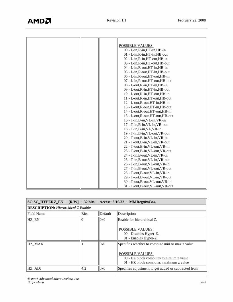
Revision 1.1 February 22, 2008
© 2008 Advanced Micro Devices, Inc. Proprietary 182
POSSIBLE VALUES:
00 - L-in,R-in,HT-in,HB-in
01 - L-in,R-in,HT-in,HB-out
02 - L-in,R-in,HT-out,HB-in
03 - L-in,R-in,HT-out,HB-out
04 - L-in,R-out,HT-in,HB-in
05 - L-in,R-out,HT-in,HB-out
06 - L-in,R-out,HT-out,HB-in
07 - L-in,R-out,HT-out,HB-out
08 - L-out,R-in,HT-in,HB-in
09 - L-out,R-in,HT-in,HB-out
10 - L-out,R-in,HT-out,HB-in
11 - L-out,R-in,HT-out,HB-out
12 - L-out,R-out,HT-in,HB-in
13 - L-out,R-out,HT-in,HB-out
14 - L-out,R-out,HT-out,HB-in
15 - L-out,R-out,HT-out,HB-out
16 - T-in,B-in,VL-in,VR-in
17 - T-in,B-in,VL-in,VR-out
18 - T-in,B-in,VL,VR-in
19 - T-in,B-in,VL-out,VR-out
20 - T-out,B-in,VL-in,VR-in
21 - T-out,B-in,VL-in,VR-out
22 - T-out,B-in,VL-out,VR-in
23 - T-out,B-in,VL-out,VR-out
24 - T-in,B-out,VL-in,VR-in
25 - T-in,B-out,VL-in,VR-out
26 - T-in,B-out,VL-out,VR-in
27 - T-in,B-out,VL-out,VR-out
28 - T-out,B-out,VL-in,VR-in
29 - T-out,B-out,VL-in,VR-out
30 - T-out,B-out,VL-out,VR-in
31 - T-out,B-out,VL-out,VR-out
SC:SC_HYPERZ_EN · [R/W] · 32 bits · Access: 8/16/32 · MMReg:0x43a4
DESCRIPTION: Hierarchical Z Enable
Field Name Bits Default Description
HZ_EN 0 0x0 Enable for hierarchical Z.
POSSIBLE VALUES:
00 - Disables Hyper-Z.
01 - Enables Hyper-Z.
HZ_MAX 1 0x0 Specifies whether to compute min or max z value
POSSIBLE VALUES:
00 - HZ block computes minimum z value
01 - HZ block computes maximum z value
HZ_ADJ 4:2 0x0 Specifies adjustment to get added or subtracted from

Revision 1.1 February 22, 2008
© 2008 Advanced Micro Devices, Inc. Proprietary 183
computed z value
POSSIBLE VALUES:
00 - Add or Subtract 1/256 << ze
01 - Add or Subtract 1/128 << ze
02 - Add or Subtract 1/64 << ze
03 - Add or Subtract 1/32 << ze
04 - Add or Subtract 1/16 << ze
05 - Add or Subtract 1/8 << ze
06 - Add or Subtract 1/4 << ze
07 - Add or Subtract 1/2 << ze
HZ_Z0MIN 5 0x0 Specifies whether vertex 0 z contains minimum z value
POSSIBLE VALUES:
00 - Vertex 0 does not contain minimum z value
01 - Vertex 0 does contain minimum z value
HZ_Z0MAX 6 0x0 Specifies whether vertex 0 z contains maximum z value
POSSIBLE VALUES:
00 - Vertex 0 does not contain maximum z value
01 - Vertex 0 does contain maximum z value
SC:SC_SCISSOR0 · [R/W] · 32 bits · Access: 8/16/32 · MMReg:0x43e0
DESCRIPTION: Scissor rectangle specification
Field Name Bits Default Description
XS0 12:0 0x0 Left hand edge of scissor rectangle
YS0 25:13 0x0 Upper edge of scissor rectangle
SC:SC_SCISSOR1 · [R/W] · 32 bits · Access: 8/16/32 · MMReg:0x43e4
DESCRIPTION: Scissor rectangle specification
Field Name Bits Default Description
XS1 12:0 0x0 Right hand edge of scissor rectangle
YS1 25:13 0x0 Lower edge of scissor rectangle
SC:SC_SCREENDOOR · [R/W] · 32 bits · Access: 8/16/32 · MMReg:0x43e8
DESCRIPTION: Screen door sample mask
Field Name Bits Default Description
SCREENDOOR 23:0 0x0 Screen door sample mask - 1 means sample may be
covered, 0 means sample is not covered

Revision 1.1 February 22, 2008
© 2008 Advanced Micro Devices, Inc. Proprietary 184
10.7 Setup Unit Registers
SU:SU_CULL_MODE · [R/W] · 32 bits · Access: 8/16/32 · MMReg:0x42b8
DESCRIPTION: Culling Enables
Field Name Bits Default Description
CULL_FRONT 0 0x0 Enable for front-face culling.
POSSIBLE VALUES:
00 - Do not cull front-facing triangles.
01 - Cull front-facing triangles.
CULL_BACK 1 0x0 Enable for back-face culling.
POSSIBLE VALUES:
00 - Do not cull back-facing triangles.
01 - Cull back-facing triangles.
FACE 2 0x0 X-Ored with cross product sign to determine positive
facing
POSSIBLE VALUES:
00 - Positive cross product is front (CCW).
01 - Negative cross product is front (CW).
SU:SU_DEPTH_OFFSET · [R/W] · 32 bits · Access: 8/16/32 · MMReg:0x42c4
DESCRIPTION: SU Depth Offset value
Field Name Bits Default Description
OFFSET 31:0 0x0 SPFP Floating point applied to depth before conversion
to FXP.
SU:SU_DEPTH_SCALE · [R/W] · 32 bits · Access: 8/16/32 · MMReg:0x42c0
DESCRIPTION: SU Depth Scale value
Field Name Bits Default Description
SCALE 31:0 0x3F800000 SPFP Floating point applied to depth before conversion
to FXP.
SU:SU_POLY_OFFSET_BACK_OFFSET · [R/W] · 32 bits · Access: 8/16/32 · MMReg:0x42b0
DESCRIPTION: Back-Facing Polygon Offset Offset
Field Name Bits Default Description
OFFSET 31:0 0x0 Specifies polygon offset offset for back-facing polygons;
32b IEEE float format; applied after Z scale & offset (0
to 2^24-1 range)

Revision 1.1 February 22, 2008
© 2008 Advanced Micro Devices, Inc. Proprietary 185
SU:SU_POLY_OFFSET_BACK_SCALE · [R/W] · 32 bits · Access: 8/16/32 · MMReg:0x42ac
DESCRIPTION: Back-Facing Polygon Offset Scale
Field Name Bits Default Description
SCALE 31:0 0x0 Specifies polygon offset scale for back-facing polygons;
32-bit IEEE float format; applied after Z scale & offset
(0 to 2^24-1 range); slope computed in subpixels (1/12 or
1/16)
SU:SU_POLY_OFFSET_ENABLE · [R/W] · 32 bits · Access: 8/16/32 · MMReg:0x42b4
DESCRIPTION: Enables for polygon offset
Field Name Bits Default Description
FRONT_ENABLE 0 0x0 Enables front facing polygon`s offset.
POSSIBLE VALUES:
00 - Disable front offset.
01 - Enable front offset.
BACK_ENABLE 1 0x0 Enables back facing polygon`s offset.
POSSIBLE VALUES:
00 - Disable back offset.
01 - Enable back offset.
PARA_ENABLE 2 0x0 Forces all parallelograms to have FRONT_FACING for
poly offset -- Need to have FRONT_ENABLE also set to
have Z offset for parallelograms.
POSSIBLE VALUES:
00 - Disable front offset for parallelograms.
01 - Enable front offset for parallelograms.
SU:SU_POLY_OFFSET_FRONT_OFFSET · [R/W] · 32 bits · Access: 8/16/32 · MMReg:0x42a8
DESCRIPTION: Front-Facing Polygon Offset Offset
Field Name Bits Default Description
OFFSET 31:0 0x0 Specifies polygon offset offset for front-facing polygons;
32b IEEE float format; applied after Z scale & offset (0
to 2^24-1 range)
SU:SU_POLY_OFFSET_FRONT_SCALE · [R/W] · 32 bits · Access: 8/16/32 · MMReg:0x42a4
DESCRIPTION: Front-Facing Polygon Offset Scale
Field Name Bits Default Description
SCALE 31:0 0x0 Specifies polygon offset scale for front-facing polygons;
32b IEEE float format; applied after Z scale & offset (0
to 2^24-1 range); slope computed in subpixels (1/12 or
1/16)

Revision 1.1 February 22, 2008
© 2008 Advanced Micro Devices, Inc. Proprietary 186
SU:SU_REG_DEST · [R/W] · 32 bits · Access: 8/16/32 · MMReg:0x42c8
DESCRIPTION: SU Raster pipe destination select for registers
Field Name Bits Default Description
SELECT 3:0 0xF Register read/write destination select: b0: logical pipe0,
b1: logical pipe1, b2: logical pipe2 and b3: logical pipe3
SU:SU_TEX_WRAP · [R/W] · 32 bits · Access: 8/16/32 · MMReg:0x42a0
DESCRIPTION: Enables for Cylindrical Wrapping
Field Name Bits Default Description
T0C0 0 0x0 tNcM -- Enable texture wrapping on component M
(S,T,R,Q) of texture N.
POSSIBLE VALUES:
00 - Disable cylindrical wrapping.
01 - Enable cylindrical wrapping.
T0C1 1 0x0 tNcM -- Enable texture wrapping on component M
(S,T,R,Q) of texture N.
POSSIBLE VALUES:
00 - Disable cylindrical wrapping.
01 - Enable cylindrical wrapping.
T0C2 2 0x0 tNcM -- Enable texture wrapping on component M
(S,T,R,Q) of texture N.
POSSIBLE VALUES:
00 - Disable cylindrical wrapping.
01 - Enable cylindrical wrapping.
T0C3 3 0x0 tNcM -- Enable texture wrapping on component M
(S,T,R,Q) of texture N.
POSSIBLE VALUES:
00 - Disable cylindrical wrapping.
01 - Enable cylindrical wrapping.
T1C0 4 0x0 tNcM -- Enable texture wrapping on component M
(S,T,R,Q) of texture N.
POSSIBLE VALUES:
00 - Disable cylindrical wrapping.
01 - Enable cylindrical wrapping.
T1C1 5 0x0 tNcM -- Enable texture wrapping on component M
(S,T,R,Q) of texture N.
POSSIBLE VALUES:
00 - Disable cylindrical wrapping.
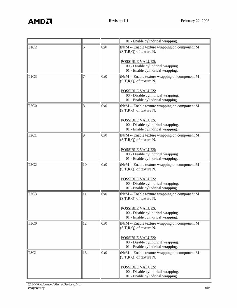
Revision 1.1 February 22, 2008
© 2008 Advanced Micro Devices, Inc. Proprietary 187
01 - Enable cylindrical wrapping.
T1C2 6 0x0 tNcM -- Enable texture wrapping on component M
(S,T,R,Q) of texture N.
POSSIBLE VALUES:
00 - Disable cylindrical wrapping.
01 - Enable cylindrical wrapping.
T1C3 7 0x0 tNcM -- Enable texture wrapping on component M
(S,T,R,Q) of texture N.
POSSIBLE VALUES:
00 - Disable cylindrical wrapping.
01 - Enable cylindrical wrapping.
T2C0 8 0x0 tNcM -- Enable texture wrapping on component M
(S,T,R,Q) of texture N.
POSSIBLE VALUES:
00 - Disable cylindrical wrapping.
01 - Enable cylindrical wrapping.
T2C1 9 0x0 tNcM -- Enable texture wrapping on component M
(S,T,R,Q) of texture N.
POSSIBLE VALUES:
00 - Disable cylindrical wrapping.
01 - Enable cylindrical wrapping.
T2C2 10 0x0 tNcM -- Enable texture wrapping on component M
(S,T,R,Q) of texture N.
POSSIBLE VALUES:
00 - Disable cylindrical wrapping.
01 - Enable cylindrical wrapping.
T2C3 11 0x0 tNcM -- Enable texture wrapping on component M
(S,T,R,Q) of texture N.
POSSIBLE VALUES:
00 - Disable cylindrical wrapping.
01 - Enable cylindrical wrapping.
T3C0 12 0x0 tNcM -- Enable texture wrapping on component M
(S,T,R,Q) of texture N.
POSSIBLE VALUES:
00 - Disable cylindrical wrapping.
01 - Enable cylindrical wrapping.
T3C1 13 0x0 tNcM -- Enable texture wrapping on component M
(S,T,R,Q) of texture N.
POSSIBLE VALUES:
00 - Disable cylindrical wrapping.
01 - Enable cylindrical wrapping.

Revision 1.1 February 22, 2008
© 2008 Advanced Micro Devices, Inc. Proprietary 188
T3C2 14 0x0 tNcM -- Enable texture wrapping on component M
(S,T,R,Q) of texture N.
POSSIBLE VALUES:
00 - Disable cylindrical wrapping.
01 - Enable cylindrical wrapping.
T3C3 15 0x0 tNcM -- Enable texture wrapping on component M
(S,T,R,Q) of texture N.
POSSIBLE VALUES:
00 - Disable cylindrical wrapping.
01 - Enable cylindrical wrapping.
T4C0 16 0x0 tNcM -- Enable texture wrapping on component M
(S,T,R,Q) of texture N.
POSSIBLE VALUES:
00 - Disable cylindrical wrapping.
01 - Enable cylindrical wrapping.
T4C1 17 0x0 tNcM -- Enable texture wrapping on component M
(S,T,R,Q) of texture N.
POSSIBLE VALUES:
00 - Disable cylindrical wrapping.
01 - Enable cylindrical wrapping.
T4C2 18 0x0 tNcM -- Enable texture wrapping on component M
(S,T,R,Q) of texture N.
POSSIBLE VALUES:
00 - Disable cylindrical wrapping.
01 - Enable cylindrical wrapping.
T4C3 19 0x0 tNcM -- Enable texture wrapping on component M
(S,T,R,Q) of texture N.
POSSIBLE VALUES:
00 - Disable cylindrical wrapping.
01 - Enable cylindrical wrapping.
T5C0 20 0x0 tNcM -- Enable texture wrapping on component M
(S,T,R,Q) of texture N.
POSSIBLE VALUES:
00 - Disable cylindrical wrapping.
01 - Enable cylindrical wrapping.
T5C1 21 0x0 tNcM -- Enable texture wrapping on component M
(S,T,R,Q) of texture N.
POSSIBLE VALUES:
00 - Disable cylindrical wrapping.
01 - Enable cylindrical wrapping.
T5C2 22 0x0 tNcM -- Enable texture wrapping on component M

Revision 1.1 February 22, 2008
© 2008 Advanced Micro Devices, Inc. Proprietary 189
(S,T,R,Q) of texture N.
POSSIBLE VALUES:
00 - Disable cylindrical wrapping.
01 - Enable cylindrical wrapping.
T5C3 23 0x0 tNcM -- Enable texture wrapping on component M
(S,T,R,Q) of texture N.
POSSIBLE VALUES:
00 - Disable cylindrical wrapping.
01 - Enable cylindrical wrapping.
T6C0 24 0x0 tNcM -- Enable texture wrapping on component M
(S,T,R,Q) of texture N.
POSSIBLE VALUES:
00 - Disable cylindrical wrapping.
01 - Enable cylindrical wrapping.
T6C1 25 0x0 tNcM -- Enable texture wrapping on component M
(S,T,R,Q) of texture N.
POSSIBLE VALUES:
00 - Disable cylindrical wrapping.
01 - Enable cylindrical wrapping.
T6C2 26 0x0 tNcM -- Enable texture wrapping on component M
(S,T,R,Q) of texture N.
POSSIBLE VALUES:
00 - Disable cylindrical wrapping.
01 - Enable cylindrical wrapping.
T6C3 27 0x0 tNcM -- Enable texture wrapping on component M
(S,T,R,Q) of texture N.
POSSIBLE VALUES:
00 - Disable cylindrical wrapping.
01 - Enable cylindrical wrapping.
T7C0 28 0x0 tNcM -- Enable texture wrapping on component M
(S,T,R,Q) of texture N.
POSSIBLE VALUES:
00 - Disable cylindrical wrapping.
01 - Enable cylindrical wrapping.
T7C1 29 0x0 tNcM -- Enable texture wrapping on component M
(S,T,R,Q) of texture N.
POSSIBLE VALUES:
00 - Disable cylindrical wrapping.
01 - Enable cylindrical wrapping.
T7C2 30 0x0 tNcM -- Enable texture wrapping on component M
(S,T,R,Q) of texture N.
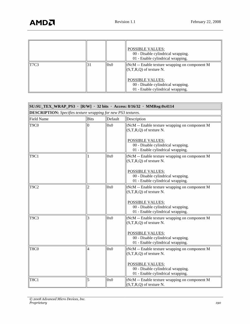
Revision 1.1 February 22, 2008
© 2008 Advanced Micro Devices, Inc. Proprietary 190
POSSIBLE VALUES:
00 - Disable cylindrical wrapping.
01 - Enable cylindrical wrapping.
T7C3 31 0x0 tNcM -- Enable texture wrapping on component M
(S,T,R,Q) of texture N.
POSSIBLE VALUES:
00 - Disable cylindrical wrapping.
01 - Enable cylindrical wrapping.
SU:SU_TEX_WRAP_PS3 · [R/W] · 32 bits · Access: 8/16/32 · MMReg:0x4114
DESCRIPTION: Specifies texture wrapping for new PS3 textures.
Field Name Bits Default Description
T9C0 0 0x0 tNcM -- Enable texture wrapping on component M
(S,T,R,Q) of texture N.
POSSIBLE VALUES:
00 - Disable cylindrical wrapping.
01 - Enable cylindrical wrapping.
T9C1 1 0x0 tNcM -- Enable texture wrapping on component M
(S,T,R,Q) of texture N.
POSSIBLE VALUES:
00 - Disable cylindrical wrapping.
01 - Enable cylindrical wrapping.
T9C2 2 0x0 tNcM -- Enable texture wrapping on component M
(S,T,R,Q) of texture N.
POSSIBLE VALUES:
00 - Disable cylindrical wrapping.
01 - Enable cylindrical wrapping.
T9C3 3 0x0 tNcM -- Enable texture wrapping on component M
(S,T,R,Q) of texture N.
POSSIBLE VALUES:
00 - Disable cylindrical wrapping.
01 - Enable cylindrical wrapping.
T8C0 4 0x0 tNcM -- Enable texture wrapping on component M
(S,T,R,Q) of texture N.
POSSIBLE VALUES:
00 - Disable cylindrical wrapping.
01 - Enable cylindrical wrapping.
T8C1 5 0x0 tNcM -- Enable texture wrapping on component M
(S,T,R,Q) of texture N.

Revision 1.1 February 22, 2008
© 2008 Advanced Micro Devices, Inc. Proprietary 191
POSSIBLE VALUES:
00 - Disable cylindrical wrapping.
01 - Enable cylindrical wrapping.
T8C2 6 0x0 tNcM -- Enable texture wrapping on component M
(S,T,R,Q) of texture N.
POSSIBLE VALUES:
00 - Disable cylindrical wrapping.
01 - Enable cylindrical wrapping.
T8C3 7 0x0 tNcM -- Enable texture wrapping on component M
(S,T,R,Q) of texture N.
POSSIBLE VALUES:
00 - Disable cylindrical wrapping.
01 - Enable cylindrical wrapping.
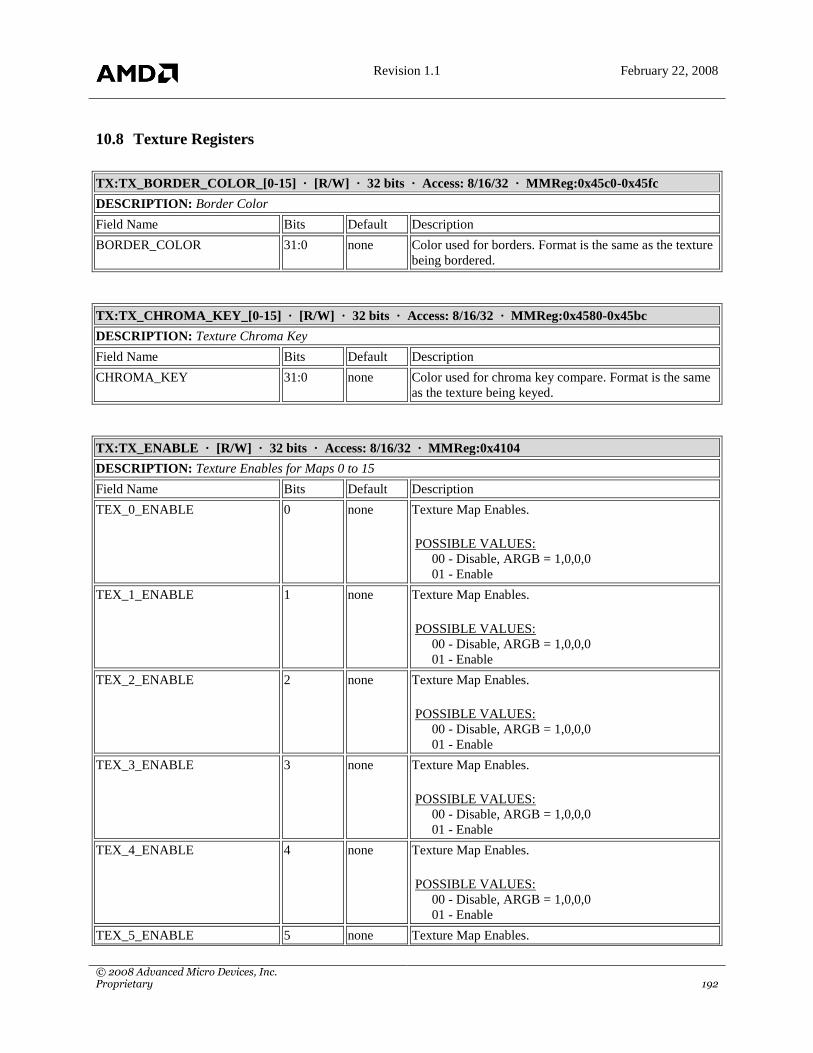
Revision 1.1 February 22, 2008
© 2008 Advanced Micro Devices, Inc. Proprietary 192
10.8 Texture Registers
TX:TX_BORDER_COLOR_[0-15] · [R/W] · 32 bits · Access: 8/16/32 · MMReg:0x45c0-0x45fc
DESCRIPTION: Border Color
Field Name Bits Default Description
BORDER_COLOR 31:0 none Color used for borders. Format is the same as the texture
being bordered.
TX:TX_CHROMA_KEY_[0-15] · [R/W] · 32 bits · Access: 8/16/32 · MMReg:0x4580-0x45bc
DESCRIPTION: Texture Chroma Key
Field Name Bits Default Description
CHROMA_KEY 31:0 none Color used for chroma key compare. Format is the same
as the texture being keyed.
TX:TX_ENABLE · [R/W] · 32 bits · Access: 8/16/32 · MMReg:0x4104
DESCRIPTION: Texture Enables for Maps 0 to 15
Field Name Bits Default Description
TEX_0_ENABLE 0 none Texture Map Enables.
POSSIBLE VALUES:
00 - Disable, ARGB = 1,0,0,0
01 - Enable
TEX_1_ENABLE 1 none Texture Map Enables.
POSSIBLE VALUES:
00 - Disable, ARGB = 1,0,0,0
01 - Enable
TEX_2_ENABLE 2 none Texture Map Enables.
POSSIBLE VALUES:
00 - Disable, ARGB = 1,0,0,0
01 - Enable
TEX_3_ENABLE 3 none Texture Map Enables.
POSSIBLE VALUES:
00 - Disable, ARGB = 1,0,0,0
01 - Enable
TEX_4_ENABLE 4 none Texture Map Enables.
POSSIBLE VALUES:
00 - Disable, ARGB = 1,0,0,0
01 - Enable
TEX_5_ENABLE 5 none Texture Map Enables.
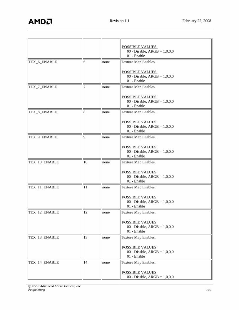
Revision 1.1 February 22, 2008
© 2008 Advanced Micro Devices, Inc. Proprietary 193
POSSIBLE VALUES:
00 - Disable, ARGB = 1,0,0,0
01 - Enable
TEX_6_ENABLE 6 none Texture Map Enables.
POSSIBLE VALUES:
00 - Disable, ARGB = 1,0,0,0
01 - Enable
TEX_7_ENABLE 7 none Texture Map Enables.
POSSIBLE VALUES:
00 - Disable, ARGB = 1,0,0,0
01 - Enable
TEX_8_ENABLE 8 none Texture Map Enables.
POSSIBLE VALUES:
00 - Disable, ARGB = 1,0,0,0
01 - Enable
TEX_9_ENABLE 9 none Texture Map Enables.
POSSIBLE VALUES:
00 - Disable, ARGB = 1,0,0,0
01 - Enable
TEX_10_ENABLE 10 none Texture Map Enables.
POSSIBLE VALUES:
00 - Disable, ARGB = 1,0,0,0
01 - Enable
TEX_11_ENABLE 11 none Texture Map Enables.
POSSIBLE VALUES:
00 - Disable, ARGB = 1,0,0,0
01 - Enable
TEX_12_ENABLE 12 none Texture Map Enables.
POSSIBLE VALUES:
00 - Disable, ARGB = 1,0,0,0
01 - Enable
TEX_13_ENABLE 13 none Texture Map Enables.
POSSIBLE VALUES:
00 - Disable, ARGB = 1,0,0,0
01 - Enable
TEX_14_ENABLE 14 none Texture Map Enables.
POSSIBLE VALUES:
00 - Disable, ARGB = 1,0,0,0

Revision 1.1 February 22, 2008
© 2008 Advanced Micro Devices, Inc. Proprietary 194
01 - Enable
TEX_15_ENABLE 15 none Texture Map Enables.
POSSIBLE VALUES:
00 - Disable, ARGB = 1,0,0,0
01 - Enable
TX:TX_FILTER0_[0-15] · [R/W] · 32 bits · Access: 8/16/32 · MMReg:0x4400-0x443c
DESCRIPTION: Texture Filter State
Field Name Bits Default Description
CLAMP_S 2:0 none Clamp mode for texture coordinates
POSSIBLE VALUES:
00 - Wrap (repeat)
01 - Mirror
02 - Clamp to last texel (0.0 to 1.0)
03 - MirrorOnce to last texel (-1.0 to 1.0)
04 - Clamp half way to border color (0.0 to 1.0)
05 - MirrorOnce half way to border color (-1.0 to 1.0)
06 - Clamp to border color (0.0 to 1.0)
07 - MirrorOnce to border color (-1.0 to 1.0)
CLAMP_T 5:3 none Clamp mode for texture coordinates
POSSIBLE VALUES:
00 - Wrap (repeat)
01 - Mirror
02 - Clamp to last texel (0.0 to 1.0)
03 - MirrorOnce to last texel (-1.0 to 1.0)
04 - Clamp half way to border color (0.0 to 1.0)
05 - MirrorOnce half way to border color (-1.0 to 1.0)
06 - Clamp to border color (0.0 to 1.0)
07 - MirrorOnce to border color (-1.0 to 1.0)
CLAMP_R 8:6 none Clamp mode for texture coordinates
POSSIBLE VALUES:
00 - Wrap (repeat)
01 - Mirror
02 - Clamp to last texel (0.0 to 1.0)
03 - MirrorOnce to last texel (-1.0 to 1.0)
04 - Clamp half way to border color (0.0 to 1.0)
05 - MirrorOnce half way to border color (-1.0 to 1.0)
06 - Clamp to border color (0.0 to 1.0)
07 - MirrorOnce to border color (-1.0 to 1.0)
MAG_FILTER 10:9 none Filter used when texture is magnified
POSSIBLE VALUES:
00 - Filter4
01 - Point

Revision 1.1 February 22, 2008
© 2008 Advanced Micro Devices, Inc. Proprietary 195
02 - Linear
03 - Reserved
MIN_FILTER 12:11 none Filter used when texture is minified
POSSIBLE VALUES:
00 - Filter4
01 - Point
02 - Linear
03 - Reserved
MIP_FILTER 14:13 none Filter used between mipmap levels
POSSIBLE VALUES:
00 - None
01 - Point
02 - Linear
03 - Reserved
VOL_FILTER 16:15 none Filter used between layers of a volume
POSSIBLE VALUES:
00 - None (no filter specifed, select from MIN/MAG
filters)
01 - Point
02 - Linear
03 - Reserved
MAX_MIP_LEVEL 20:17 none LOD index of largest (finest) mipmap to use (0 is
largest). Ranges from 0 to NUM_LEVELS.
Reserved 23:21 none
ID 31:28 none Logical id for this physical texture
TX:TX_FILTER1_[0-15] · [R/W] · 32 bits · Access: 8/16/32 · MMReg:0x4440-0x447c
DESCRIPTION: Texture Filter State
Field Name Bits Default Description
CHROMA_KEY_MODE 1:0 none Chroma Key Mode
POSSIBLE VALUES:
00 - Disable
01 - ChromaKey (kill pixel if any sample matches
chroma key)
02 - ChromaKeyBlend (set sample to 0 if it matches
chroma key)
MC_ROUND 2 none Bilinear rounding mode
POSSIBLE VALUES:
00 - Normal rounding on all components (+0.5)
01 - MPEG4 rounding on all components (+0.25)
LOD_BIAS 12:3 none (s4.5). Ranges from -16.0 to 15.99. Mipmap LOD bias
measured in mipmap levels. Added to the signed,

Revision 1.1 February 22, 2008
© 2008 Advanced Micro Devices, Inc. Proprietary 196
computed LOD before the LOD is clamped.
Reserved 13 none
MC_COORD_TRUNCATE 14 none MPEG coordinate truncation mode
POSSIBLE VALUES:
00 - Dont truncate coordinate fractions.
01 - Truncate coordinate fractions to 0.0 and 0.5 for
MPEG
TRI_PERF 16:15 none Apply slope and bias to trilerp fraction to reduce the
number of 2-level fetches for trilinear. Should only be
used if MIP_FILTER is LINEAR.
POSSIBLE VALUES:
00 - Breakpoint=0/8. lfrac_out = lfrac_in
01 - Breakpoint=1/8. lfrac_out = clamp(4/3*lfrac_in -
1/6)
02 - Breakpoint=1/4. lfrac_out = clamp(2*lfrac_in -
1/2)
03 - Breakpoint=3/8. lfrac_out = clamp(4*lfrac_in -
3/2)
Reserved 19:17 none Set to 0
Reserved 20 none Set to 0
Reserved 21 none Set to 0
MACRO_SWITCH 22 none If enabled, addressing switches to macro-linear when
image width is <= 8 micro-tiles. If disabled, functionality
is same as RV350, switch to macro-linear when image
width is < 8 micro-tiles.
POSSIBLE VALUES:
00 - RV350 mode
01 - Switch from macro-tiled to macro-linear when
(width <= 8 micro-tiles)
Reserved 28:23 none
Reserved 29 none
Reserved 30 none
BORDER_FIX 31 none To fix issues when using non-square mipmaps, with
border_color, and extreme minification.
POSSIBLE VALUES:
00 - R3xx R4xx mode
01 - Stop right shifting coord once mip size is pinned
to one
TX:TX_FILTER4 · [R/W] · 32 bits · Access: 8/16/32 · MMReg:0x4110
DESCRIPTION: Filter4 Kernel
Field Name Bits Default Description

Revision 1.1 February 22, 2008
© 2008 Advanced Micro Devices, Inc. Proprietary 197
WEIGHT_1 10:0 none (s1.9). Bottom or Right weight of pair.
WEIGHT_0 21:11 none (s1.9). Top or Left weight of pair.
WEIGHT_PAIR 22 none Indicates which pair of weights within phase to load.
POSSIBLE VALUES:
00 - Top or Left
01 - Bottom or Right
PHASE 26:23 none Indicates which of 9 phases to load
DIRECTION 27 none Indicates whether to load the horizontal or vertical
weights
POSSIBLE VALUES:
00 - Horizontal
01 - Vertical
TX:TX_FORMAT0_[0-15] · [R/W] · 32 bits · Access: 8/16/32 · MMReg:0x4480-0x44bc
DESCRIPTION: Texture Format State
Field Name Bits Default Description
TXWIDTH 10:0 none Image width - 1. The largest image is 4096 texels. When
wrapping or mirroring, must be a power of 2. When
mipmapping, must be a power of 2 or padded to a power
of 2 in memory. Can always be non-square, except for
cube maps which must be square.
TXHEIGHT 21:11 none Image height - 1. The largest image is 4096 texels. When
wrapping or mirroring, must be a power of 2. When
mipmapping, must be a power of 2 or padded to a power
of 2 in memory. Can always be non-square, except for
cube maps which must be square.
TXDEPTH 25:22 none LOG2(depth) of volume texture
NUM_LEVELS 29:26 none Number of mipmap levels minus 1. Ranges from 0 to 12.
Equivalent to LOD index of smallest (coarsest) mipmap
to use.
PROJECTED 30 none Specifies whether texture coords are projected.
POSSIBLE VALUES:
00 - Non-Projected
01 - Projected
TXPITCH_EN 31 none Indicates when TXPITCH should be used instead of
TXWIDTH for image addressing
POSSIBLE VALUES:
00 - Use TXWIDTH for image addressing
01 - Use TXPITCH for image addressing
TX:TX_FORMAT1_[0-15] · [R/W] · 32 bits · Access: 8/16/32 · MMReg:0x44c0-0x44fc

Revision 1.1 February 22, 2008
© 2008 Advanced Micro Devices, Inc. Proprietary 198
DESCRIPTION: Texture Format State
Field Name Bits Default Description
TXFORMAT 4:0 none Texture Format. Components are numbered right to left.
Parenthesis indicate typical uses of each format.
POSSIBLE VALUES:
00 - TX_FMT_8 or TX_FMT_1 (if
TX_FORMAT2.TXFORMAT_MSB is set)
01 - TX_FMT_16 or TX_FMT_1_REVERSE (if
TX_FORMAT2.TXFORMAT_MSB is set)
02 - TX_FMT_4_4 or TX_FMT_10 (if
TX_FORMAT2.TXFORMAT_MSB is set)
03 - TX_FMT_8_8 or TX_FMT_10_10 (if
TX_FORMAT2.TXFORMAT_MSB is set)
04 - TX_FMT_16_16 or TX_FMT_10_10_10_10 (if
TX_FORMAT2.TXFORMAT_MSB is set)
05 - TX_FMT_3_3_2 or TX_FMT_ATI1N (if
TX_FORMAT2.TXFORMAT_MSB is set)
06 - TX_FMT_5_6_5
07 - TX_FMT_6_5_5
08 - TX_FMT_11_11_10
09 - TX_FMT_10_11_11
10 - TX_FMT_4_4_4_4
11 - TX_FMT_1_5_5_5
12 - TX_FMT_8_8_8_8
13 - TX_FMT_2_10_10_10
14 - TX_FMT_16_16_16_16
15 - Reserved
16 - Reserved
17 - Reserved
18 - TX_FMT_Y8
19 - TX_FMT_AVYU444
20 - TX_FMT_VYUY422
21 - TX_FMT_YVYU422
22 - TX_FMT_16_MPEG
23 - TX_FMT_16_16_MPEG
24 - TX_FMT_16f
25 - TX_FMT_16f_16f
26 - TX_FMT_16f_16f_16f_16f
27 - TX_FMT_32f
28 - TX_FMT_32f_32f
29 - TX_FMT_32f_32f_32f_32f
30 - TX_FMT_W24_FP
31 - TX_FMT_ATI2N
SIGNED_COMP0 5 none Component filter should interpret texel data as signed or
unsigned. (Ignored for Y/YUV formats.)
POSSIBLE VALUES:
00 - Component filter should interpret texel data as
unsigned
01 - Component filter should interpret texel data as
signed

Revision 1.1 February 22, 2008
© 2008 Advanced Micro Devices, Inc. Proprietary 199
SIGNED_COMP1 6 none Component filter should interpret texel data as signed or
unsigned. (Ignored for Y/YUV formats.)
POSSIBLE VALUES:
00 - Component filter should interpret texel data as
unsigned
01 - Component filter should interpret texel data as
signed
SIGNED_COMP2 7 none Component filter should interpret texel data as signed or
unsigned. (Ignored for Y/YUV formats.)
POSSIBLE VALUES:
00 - Component filter should interpret texel data as
unsigned
01 - Component filter should interpret texel data as
signed
SIGNED_COMP3 8 none Component filter should interpret texel data as signed or
unsigned. (Ignored for Y/YUV formats.)
POSSIBLE VALUES:
00 - Component filter should interpret texel data as
unsigned
01 - Component filter should interpret texel data as
signed
SEL_ALPHA 11:9 none Specifies swizzling for each channel at the input of the
pixel shader. (Ignored for Y/YUV formats.)
POSSIBLE VALUES:
00 - Select Texture Component0.
01 - Select Texture Component1.
02 - Select Texture Component2.
03 - Select Texture Component3.
04 - Select the value 0.
05 - Select the value 1.
SEL_RED 14:12 none Specifies swizzling for each channel at the input of the
pixel shader. (Ignored for Y/YUV formats.)
POSSIBLE VALUES:
00 - Select Texture Component0.
01 - Select Texture Component1.
02 - Select Texture Component2.
03 - Select Texture Component3.
04 - Select the value 0.
05 - Select the value 1.
SEL_GREEN 17:15 none Specifies swizzling for each channel at the input of the
pixel shader. (Ignored for Y/YUV formats.)
POSSIBLE VALUES:
00 - Select Texture Component0.
01 - Select Texture Component1.
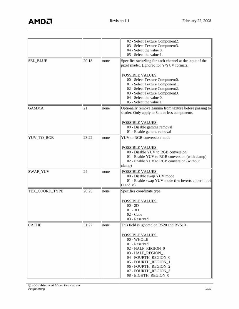
Revision 1.1 February 22, 2008
© 2008 Advanced Micro Devices, Inc. Proprietary 200
02 - Select Texture Component2.
03 - Select Texture Component3.
04 - Select the value 0.
05 - Select the value 1.
SEL_BLUE 20:18 none Specifies swizzling for each channel at the input of the
pixel shader. (Ignored for Y/YUV formats.)
POSSIBLE VALUES:
00 - Select Texture Component0.
01 - Select Texture Component1.
02 - Select Texture Component2.
03 - Select Texture Component3.
04 - Select the value 0.
05 - Select the value 1.
GAMMA 21 none Optionally remove gamma from texture before passing to
shader. Only apply to 8bit or less components.
POSSIBLE VALUES:
00 - Disable gamma removal
01 - Enable gamma removal
YUV_TO_RGB 23:22 none YUV to RGB conversion mode
POSSIBLE VALUES:
00 - Disable YUV to RGB conversion
01 - Enable YUV to RGB conversion (with clamp)
02 - Enable YUV to RGB conversion (without
clamp)
SWAP_YUV 24 none POSSIBLE VALUES:
00 - Disable swap YUV mode
01 - Enable swap YUV mode (hw inverts upper bit of
U and V)
TEX_COORD_TYPE 26:25 none Specifies coordinate type.
POSSIBLE VALUES:
00 - 2D
01 - 3D
02 - Cube
03 - Reserved
CACHE 31:27 none This field is ignored on R520 and RV510.
POSSIBLE VALUES:
00 - WHOLE
01 - Reserved
02 - HALF_REGION_0
03 - HALF_REGION_1
04 - FOURTH_REGION_0
05 - FOURTH_REGION_1
06 - FOURTH_REGION_2
07 - FOURTH_REGION_3
08 - EIGHTH_REGION_0
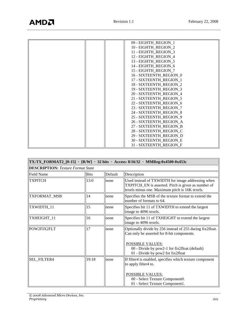
Revision 1.1 February 22, 2008
© 2008 Advanced Micro Devices, Inc. Proprietary 201
09 - EIGHTH_REGION_1
10 - EIGHTH_REGION_2
11 - EIGHTH_REGION_3
12 - EIGHTH_REGION_4
13 - EIGHTH_REGION_5
14 - EIGHTH_REGION_6
15 - EIGHTH_REGION_7
16 - SIXTEENTH_REGION_0
17 - SIXTEENTH_REGION_1
18 - SIXTEENTH_REGION_2
19 - SIXTEENTH_REGION_3
20 - SIXTEENTH_REGION_4
21 - SIXTEENTH_REGION_5
22 - SIXTEENTH_REGION_6
23 - SIXTEENTH_REGION_7
24 - SIXTEENTH_REGION_8
25 - SIXTEENTH_REGION_9
26 - SIXTEENTH_REGION_A
27 - SIXTEENTH_REGION_B
28 - SIXTEENTH_REGION_C
29 - SIXTEENTH_REGION_D
30 - SIXTEENTH_REGION_E
31 - SIXTEENTH_REGION_F
TX:TX_FORMAT2_[0-15] · [R/W] · 32 bits · Access: 8/16/32 · MMReg:0x4500-0x453c
DESCRIPTION: Texture Format State
Field Name Bits Default Description
TXPITCH 13:0 none Used instead of TXWIDTH for image addressing when
TXPITCH_EN is asserted. Pitch is given as number of
texels minus one. Maximum pitch is 16K texels.
TXFORMAT_MSB 14 none Specifies the MSB of the texture format to extend the
number of formats to 64.
TXWIDTH_11 15 none Specifies bit 11 of TXWIDTH to extend the largest
image to 4096 texels.
TXHEIGHT_11 16 none Specifies bit 11 of TXHEIGHT to extend the largest
image to 4096 texels.
POW2FIX2FLT 17 none Optionally divide by 256 instead of 255 during fix2float.
Can only be asserted for 8-bit components.
POSSIBLE VALUES:
00 - Divide by pow2-1 for fix2float (default)
01 - Divide by pow2 for fix2float
SEL_FILTER4 19:18 none If filter4 is enabled, specifies which texture component
to apply filter4 to.
POSSIBLE VALUES:
00 - Select Texture Component0.
01 - Select Texture Component1.

Revision 1.1 February 22, 2008
© 2008 Advanced Micro Devices, Inc. Proprietary 202
02 - Select Texture Component2.
03 - Select Texture Component3.
TX:TX_INVALTAGS · [R/W] · 32 bits · Access: 8/16/32 · MMReg:0x4100
DESCRIPTION: Invalidate texture cache tags
Field Name Bits Default Description
RESERVED 31:0 none Unused
TX:TX_OFFSET_[0-15] · [R/W] · 32 bits · Access: 8/16/32 · MMReg:0x4540-0x457c
DESCRIPTION: Texture Offset State
Field Name Bits Default Description
ENDIAN_SWAP 1:0 none Endian Control
POSSIBLE VALUES:
00 - No swap
01 - 16 bit swap
02 - 32 bit swap
03 - Half-DWORD swap
MACRO_TILE 2 none Macro Tile Control
POSSIBLE VALUES:
00 - 2KB page is linear
01 - 2KB page is tiled
MICRO_TILE 4:3 none Micro Tile Control
POSSIBLE VALUES:
00 - 32 byte cache line is linear
01 - 32 byte cache line is tiled
02 - 32 byte cache line is tiled square (only applies to
16-bit texel)
03 - Reserved
TXOFFSET 31:5 none 32-byte aligned pointer to base map
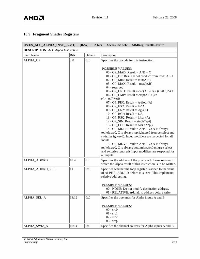
Revision 1.1 February 22, 2008
© 2008 Advanced Micro Devices, Inc. Proprietary 203
10.9 Fragment Shader Registers
US:US_ALU_ALPHA_INST_[0-511] · [R/W] · 32 bits · Access: 8/16/32 · MMReg:0xa800-0xaffc
DESCRIPTION: ALU Alpha Instruction
Field Name Bits Default Description
ALPHA_OP 3:0 0x0 Specifies the opcode for this instruction.
POSSIBLE VALUES:
00 - OP_MAD: Result = A*B + C
01 - OP_DP: Result = dot product from RGB ALU
02 - OP_MIN: Result = min(A,B)
03 - OP_MAX: Result = max(A,B)
04 - reserved
05 - OP_CND: Result = cnd(A,B,C) = (C>0.5)?A:B
06 - OP_CMP: Result = cmp(A,B,C) =
(C>=0.0)?A:B
07 - OP_FRC: Result = A-floor(A)
08 - OP_EX2: Result = 2^^A
09 - OP_LN2: Result = log2(A)
10 - OP_RCP: Result = 1/A
11 - OP_RSQ: Result = 1/sqrt(A)
12 - OP_SIN: Result = sin(A*2pi)
13 - OP_COS: Result = cos(A*2pi)
14 - OP_MDH: Result = A*B + C; A is always
topleft.src0, C is always topright.src0 (source select and
swizzles ignored). Input modifiers are respected for all
inputs.
15 - OP_MDV: Result = A*B + C; A is always
topleft.src0, C is always bottomleft.src0 (source select
and swizzles ignored). Input modifiers are respected for
all inputs.
ALPHA_ADDRD 10:4 0x0 Specifies the address of the pixel stack frame register to
which the Alpha result of this instruction is to be written.
ALPHA_ADDRD_REL 11 0x0 Specifies whether the loop register is added to the value
of ALPHA_ADDRD before it is used. This implements
relative addressing.
POSSIBLE VALUES:
00 - NONE: Do not modify destination address.
01 - RELATIVE: Add aL to address before write.
ALPHA_SEL_A 13:12 0x0 Specifies the operands for Alpha inputs A and B.
POSSIBLE VALUES:
00 - src0
01 - src1
02 - src2
03 - srcp
ALPHA_SWIZ_A 16:14 0x0 Specifies the channel sources for Alpha inputs A and B.

Revision 1.1 February 22, 2008
© 2008 Advanced Micro Devices, Inc. Proprietary 204
POSSIBLE VALUES:
00 - Red
01 - Green
02 - Blue
03 - Alpha
04 - Zero
05 - Half
06 - One
07 - Unused
ALPHA_MOD_A 18:17 0x0 Specifies the input modifiers for Alpha inputs A and B.
POSSIBLE VALUES:
00 - NOP: Do not modify input
01 - NEG: Negate input
02 - ABS: Take absolute value of input
03 - NAB: Take negative absolute value of input
ALPHA_SEL_B 20:19 0x0 Specifies the operands for Alpha inputs A and B.
POSSIBLE VALUES:
00 - src0
01 - src1
02 - src2
03 - srcp
ALPHA_SWIZ_B 23:21 0x0 Specifies the channel sources for Alpha inputs A and B.
POSSIBLE VALUES:
00 - Red
01 - Green
02 - Blue
03 - Alpha
04 - Zero
05 - Half
06 - One
07 - Unused
ALPHA_MOD_B 25:24 0x0 Specifies the input modifiers for Alpha inputs A and B.
POSSIBLE VALUES:
00 - NOP: Do not modify input
01 - NEG: Negate input
02 - ABS: Take absolute value of input
03 - NAB: Take negative absolute value of input
OMOD 28:26 0x0 Specifies the output modifier for this instruction.
POSSIBLE VALUES:
00 - Result * 1
01 - Result * 2
02 - Result * 4
03 - Result * 8
04 - Result / 2
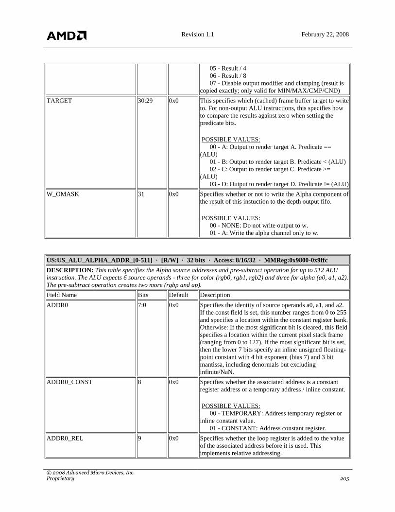
Revision 1.1 February 22, 2008
© 2008 Advanced Micro Devices, Inc. Proprietary 205
05 - Result / 4
06 - Result / 8
07 - Disable output modifier and clamping (result is
copied exactly; only valid for MIN/MAX/CMP/CND)
TARGET 30:29 0x0 This specifies which (cached) frame buffer target to write
to. For non-output ALU instructions, this specifies how
to compare the results against zero when setting the
predicate bits.
POSSIBLE VALUES:
00 - A: Output to render target A. Predicate ==
(ALU)
01 - B: Output to render target B. Predicate < (ALU)
02 - C: Output to render target C. Predicate >=
(ALU)
03 - D: Output to render target D. Predicate != (ALU)
W_OMASK 31 0x0 Specifies whether or not to write the Alpha component of
the result of this instuction to the depth output fifo.
POSSIBLE VALUES:
00 - NONE: Do not write output to w.
01 - A: Write the alpha channel only to w.
US:US_ALU_ALPHA_ADDR_[0-511] · [R/W] · 32 bits · Access: 8/16/32 · MMReg:0x9800-0x9ffc
DESCRIPTION: This table specifies the Alpha source addresses and pre-subtract operation for up to 512 ALU
instruction. The ALU expects 6 source operands - three for color (rgb0, rgb1, rgb2) and three for alpha (a0, a1, a2).
The pre-subtract operation creates two more (rgbp and ap).
Field Name Bits Default Description
ADDR0 7:0 0x0 Specifies the identity of source operands a0, a1, and a2.
If the const field is set, this number ranges from 0 to 255
and specifies a location within the constant register bank.
Otherwise: If the most significant bit is cleared, this field
specifies a location within the current pixel stack frame
(ranging from 0 to 127). If the most significant bit is set,
then the lower 7 bits specify an inline unsigned floating-
point constant with 4 bit exponent (bias 7) and 3 bit
mantissa, including denormals but excluding
infinite/NaN.
ADDR0_CONST 8 0x0 Specifies whether the associated address is a constant
register address or a temporary address / inline constant.
POSSIBLE VALUES:
00 - TEMPORARY: Address temporary register or
inline constant value.
01 - CONSTANT: Address constant register.
ADDR0_REL 9 0x0 Specifies whether the loop register is added to the value
of the associated address before it is used. This
implements relative addressing.

Revision 1.1 February 22, 2008
© 2008 Advanced Micro Devices, Inc. Proprietary 206
POSSIBLE VALUES:
00 - NONE: Do not modify source address.
01 - RELATIVE: Add aL before lookup.
ADDR1 17:10 0x0 Specifies the identity of source operands a0, a1, and a2.
If the const field is set, this number ranges from 0 to 255
and specifies a location within the constant register bank.
Otherwise: If the most significant bit is cleared, this field
specifies a location within the current pixel stack frame
(ranging from 0 to 127). If the most significant bit is set,
then the lower 7 bits specify an inline unsigned floating-
point constant with 4 bit exponent (bias 7) and 3 bit
mantissa, including denormals but excluding
infinite/NaN.
ADDR1_CONST 18 0x0 Specifies whether the associated address is a constant
register address or a temporary address / inline constant.
POSSIBLE VALUES:
00 - TEMPORARY: Address temporary register or
inline constant value.
01 - CONSTANT: Address constant register.
ADDR1_REL 19 0x0 Specifies whether the loop register is added to the value
of the associated address before it is used. This
implements relative addressing.
POSSIBLE VALUES:
00 - NONE: Do not modify source address.
01 - RELATIVE: Add aL before lookup.
ADDR2 27:20 0x0 Specifies the identity of source operands a0, a1, and a2.
If the const field is set, this number ranges from 0 to 255
and specifies a location within the constant register bank.
Otherwise: If the most significant bit is cleared, this field
specifies a location within the current pixel stack frame
(ranging from 0 to 127). If the most significant bit is set,
then the lower 7 bits specify an inline unsigned floating-
point constant with 4 bit exponent (bias 7) and 3 bit
mantissa, including denormals but excluding
infinite/NaN.
ADDR2_CONST 28 0x0 Specifies whether the associated address is a constant
register address or a temporary address / inline constant.
POSSIBLE VALUES:
00 - TEMPORARY: Address temporary register or
inline constant value.
01 - CONSTANT: Address constant register.
ADDR2_REL 29 0x0 Specifies whether the loop register is added to the value
of the associated address before it is used. This
implements relative addressing.
POSSIBLE VALUES:
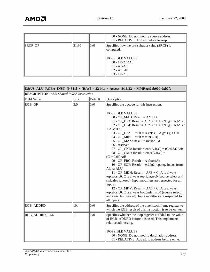
Revision 1.1 February 22, 2008
© 2008 Advanced Micro Devices, Inc. Proprietary 207
00 - NONE: Do not modify source address.
01 - RELATIVE: Add aL before lookup.
SRCP_OP 31:30 0x0 Specifies how the pre-subtract value (SRCP) is
computed.
POSSIBLE VALUES:
00 - 1.0-2.0*A0
01 - A1-A0
02 - A1+A0
03 - 1.0-A0
US:US_ALU_RGBA_INST_[0-511] · [R/W] · 32 bits · Access: 8/16/32 · MMReg:0xb000-0xb7fc
DESCRIPTION: ALU Shared RGBA Instruction
Field Name Bits Default Description
RGB_OP 3:0 0x0 Specifies the opcode for this instruction.
POSSIBLE VALUES:
00 - OP_MAD: Result = A*B + C
01 - OP_DP3: Result = A.r*B.r + A.g*B.g + A.b*B.b
02 - OP_DP4: Result = A.r*B.r + A.g*B.g + A.b*B.b
+ A.a*B.a
03 - OP_D2A: Result = A.r*B.r + A.g*B.g + C.b
04 - OP_MIN: Result = min(A,B)
05 - OP_MAX: Result = max(A,B)
06 - reserved
07 - OP_CND: Result = cnd(A,B,C) = (C>0.5)?A:B
08 - OP_CMP: Result = cmp(A,B,C) =
(C>=0.0)?A:B
09 - OP_FRC: Result = A-floor(A)
10 - OP_SOP: Result = ex2,ln2,rcp,rsq,sin,cos from
Alpha ALU
11 - OP_MDH: Result = A*B + C; A is always
topleft.src0, C is always topright.src0 (source select and
swizzles ignored). Input modifiers are respected for all
inputs.
12 - OP_MDV: Result = A*B + C; A is always
topleft.src0, C is always bottomleft.src0 (source select
and swizzles ignored). Input modifiers are respected for
all inputs.
RGB_ADDRD 10:4 0x0 Specifies the address of the pixel stack frame register to
which the RGB result of this instruction is to be written.
RGB_ADDRD_REL 11 0x0 Specifies whether the loop register is added to the value
of RGB_ADDRD before it is used. This implements
relative addressing.
POSSIBLE VALUES:
00 - NONE: Do not modify destination address.
01 - RELATIVE: Add aL to address before write.

Revision 1.1 February 22, 2008
© 2008 Advanced Micro Devices, Inc. Proprietary 208
RGB_SEL_C 13:12 0x0 Specifies the operands for RGB and Alpha input C.
POSSIBLE VALUES:
00 - src0
01 - src1
02 - src2
03 - srcp
RED_SWIZ_C 16:14 0x0 Specifies, per channel, the sources for RGB and Alpha
input C.
POSSIBLE VALUES:
00 - Red
01 - Green
02 - Blue
03 - Alpha
04 - Zero
05 - Half
06 - One
07 - Unused
GREEN_SWIZ_C 19:17 0x0 Specifies, per channel, the sources for RGB and Alpha
input C.
POSSIBLE VALUES:
00 - Red
01 - Green
02 - Blue
03 - Alpha
04 - Zero
05 - Half
06 - One
07 - Unused
BLUE_SWIZ_C 22:20 0x0 Specifies, per channel, the sources for RGB and Alpha
input C.
POSSIBLE VALUES:
00 - Red
01 - Green
02 - Blue
03 - Alpha
04 - Zero
05 - Half
06 - One
07 - Unused
RGB_MOD_C 24:23 0x0 Specifies the input modifiers for RGB and Alpha input
C.
POSSIBLE VALUES:
00 - NOP: Do not modify input
01 - NEG: Negate input
02 - ABS: Take absolute value of input
03 - NAB: Take negative absolute value of input
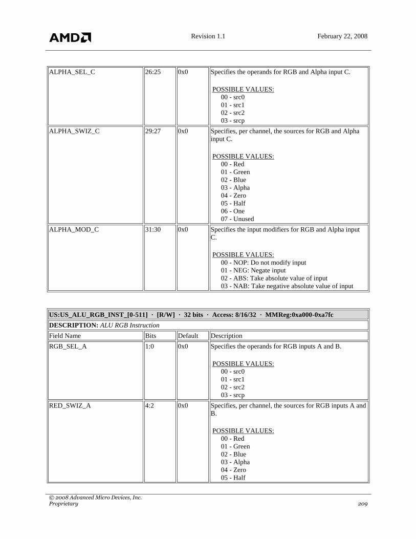
Revision 1.1 February 22, 2008
© 2008 Advanced Micro Devices, Inc. Proprietary 209
ALPHA_SEL_C 26:25 0x0 Specifies the operands for RGB and Alpha input C.
POSSIBLE VALUES:
00 - src0
01 - src1
02 - src2
03 - srcp
ALPHA_SWIZ_C 29:27 0x0 Specifies, per channel, the sources for RGB and Alpha
input C.
POSSIBLE VALUES:
00 - Red
01 - Green
02 - Blue
03 - Alpha
04 - Zero
05 - Half
06 - One
07 - Unused
ALPHA_MOD_C 31:30 0x0 Specifies the input modifiers for RGB and Alpha input
C.
POSSIBLE VALUES:
00 - NOP: Do not modify input
01 - NEG: Negate input
02 - ABS: Take absolute value of input
03 - NAB: Take negative absolute value of input
US:US_ALU_RGB_INST_[0-511] · [R/W] · 32 bits · Access: 8/16/32 · MMReg:0xa000-0xa7fc
DESCRIPTION: ALU RGB Instruction
Field Name Bits Default Description
RGB_SEL_A 1:0 0x0 Specifies the operands for RGB inputs A and B.
POSSIBLE VALUES:
00 - src0
01 - src1
02 - src2
03 - srcp
RED_SWIZ_A 4:2 0x0 Specifies, per channel, the sources for RGB inputs A and
B.
POSSIBLE VALUES:
00 - Red
01 - Green
02 - Blue
03 - Alpha
04 - Zero
05 - Half
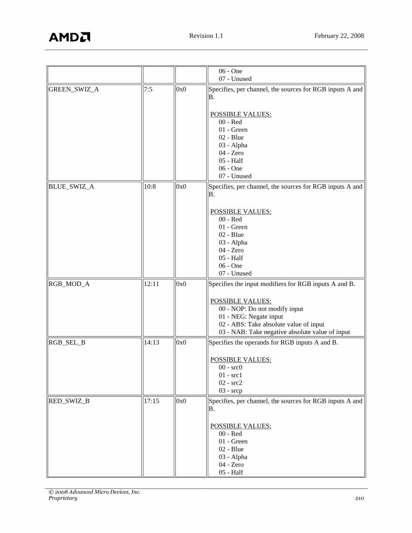
Revision 1.1 February 22, 2008
© 2008 Advanced Micro Devices, Inc. Proprietary 210
06 - One
07 - Unused
GREEN_SWIZ_A 7:5 0x0 Specifies, per channel, the sources for RGB inputs A and
B.
POSSIBLE VALUES:
00 - Red
01 - Green
02 - Blue
03 - Alpha
04 - Zero
05 - Half
06 - One
07 - Unused
BLUE_SWIZ_A 10:8 0x0 Specifies, per channel, the sources for RGB inputs A and
B.
POSSIBLE VALUES:
00 - Red
01 - Green
02 - Blue
03 - Alpha
04 - Zero
05 - Half
06 - One
07 - Unused
RGB_MOD_A 12:11 0x0 Specifies the input modifiers for RGB inputs A and B.
POSSIBLE VALUES:
00 - NOP: Do not modify input
01 - NEG: Negate input
02 - ABS: Take absolute value of input
03 - NAB: Take negative absolute value of input
RGB_SEL_B 14:13 0x0 Specifies the operands for RGB inputs A and B.
POSSIBLE VALUES:
00 - src0
01 - src1
02 - src2
03 - srcp
RED_SWIZ_B 17:15 0x0 Specifies, per channel, the sources for RGB inputs A and
B.
POSSIBLE VALUES:
00 - Red
01 - Green
02 - Blue
03 - Alpha
04 - Zero
05 - Half

Revision 1.1 February 22, 2008
© 2008 Advanced Micro Devices, Inc. Proprietary 211
06 - One
07 - Unused
GREEN_SWIZ_B 20:18 0x0 Specifies, per channel, the sources for RGB inputs A and
B.
POSSIBLE VALUES:
00 - Red
01 - Green
02 - Blue
03 - Alpha
04 - Zero
05 - Half
06 - One
07 - Unused
BLUE_SWIZ_B 23:21 0x0 Specifies, per channel, the sources for RGB inputs A and
B.
POSSIBLE VALUES:
00 - Red
01 - Green
02 - Blue
03 - Alpha
04 - Zero
05 - Half
06 - One
07 - Unused
RGB_MOD_B 25:24 0x0 Specifies the input modifiers for RGB inputs A and B.
POSSIBLE VALUES:
00 - NOP: Do not modify input
01 - NEG: Negate input
02 - ABS: Take absolute value of input
03 - NAB: Take negative absolute value of input
OMOD 28:26 0x0 Specifies the output modifier for this instruction.
POSSIBLE VALUES:
00 - Result * 1
01 - Result * 2
02 - Result * 4
03 - Result * 8
04 - Result / 2
05 - Result / 4
06 - Result / 8
07 - Disable output modifier and clamping (result is
copied exactly; only valid for MIN/MAX/CMP/CND)
TARGET 30:29 0x0 This specifies which (cached) frame buffer target to write
to. For non-output ALU instructions, this specifies how
to compare the results against zero when setting the
predicate bits.

Revision 1.1 February 22, 2008
© 2008 Advanced Micro Devices, Inc. Proprietary 212
POSSIBLE VALUES:
00 - A: Output to render target A. Predicate ==
(ALU)
01 - B: Output to render target B. Predicate < (ALU)
02 - C: Output to render target C. Predicate >=
(ALU)
03 - D: Output to render target D. Predicate != (ALU)
ALU_WMASK 31 0x0 Specifies whether to update the current ALU result.
POSSIBLE VALUES:
00 - Do not modify the current ALU result.
01 - Modify the current ALU result based on the
settings of ALU_RESULT_SEL and
ALU_RESULT_OP.
US:US_ALU_RGB_ADDR_[0-511] · [R/W] · 32 bits · Access: 8/16/32 · MMReg:0x9000-0x97fc
DESCRIPTION: This table specifies the RGB source addresses and pre-subtract operation for up to 512 ALU
instructions. The ALU expects 6 source operands - three for color (rgb0, rgb1, rgb2) and three for alpha (a0, a1,
a2). The pre-subtract operation creates two more (rgbp and ap).
Field Name Bits Default Description
ADDR0 7:0 0x0 Specifies the identity of source operands rgb0, rgb1, and
rgb2. If the const field is set, this number ranges from 0
to 255 and specifies a location within the constant
register bank. Otherwise: If the most significant bit is
cleared, this field specifies a location within the current
pixel stack frame (ranging from 0 to 127). If the most
significant bit is set, then the lower 7 bits specify an
inline unsigned floating-point constant with 4 bit
exponent (bias 7) and 3 bit mantissa, including
denormals but excluding infinite/NaN.
ADDR0_CONST 8 0x0 Specifies whether the associated address is a constant
register address or a temporary address / inline constant.
POSSIBLE VALUES:
00 - TEMPORARY: Address temporary register or
inline constant value.
01 - CONSTANT: Address constant register.
ADDR0_REL 9 0x0 Specifies whether the loop register is added to the value
of the associated address before it is used. This
implements relative addressing.
POSSIBLE VALUES:
00 - NONE: Do not modify source address.
01 - RELATIVE: Add aL before lookup.
ADDR1 17:10 0x0 Specifies the identity of source operands rgb0, rgb1, and
rgb2. If the const field is set, this number ranges from 0
to 255 and specifies a location within the constant
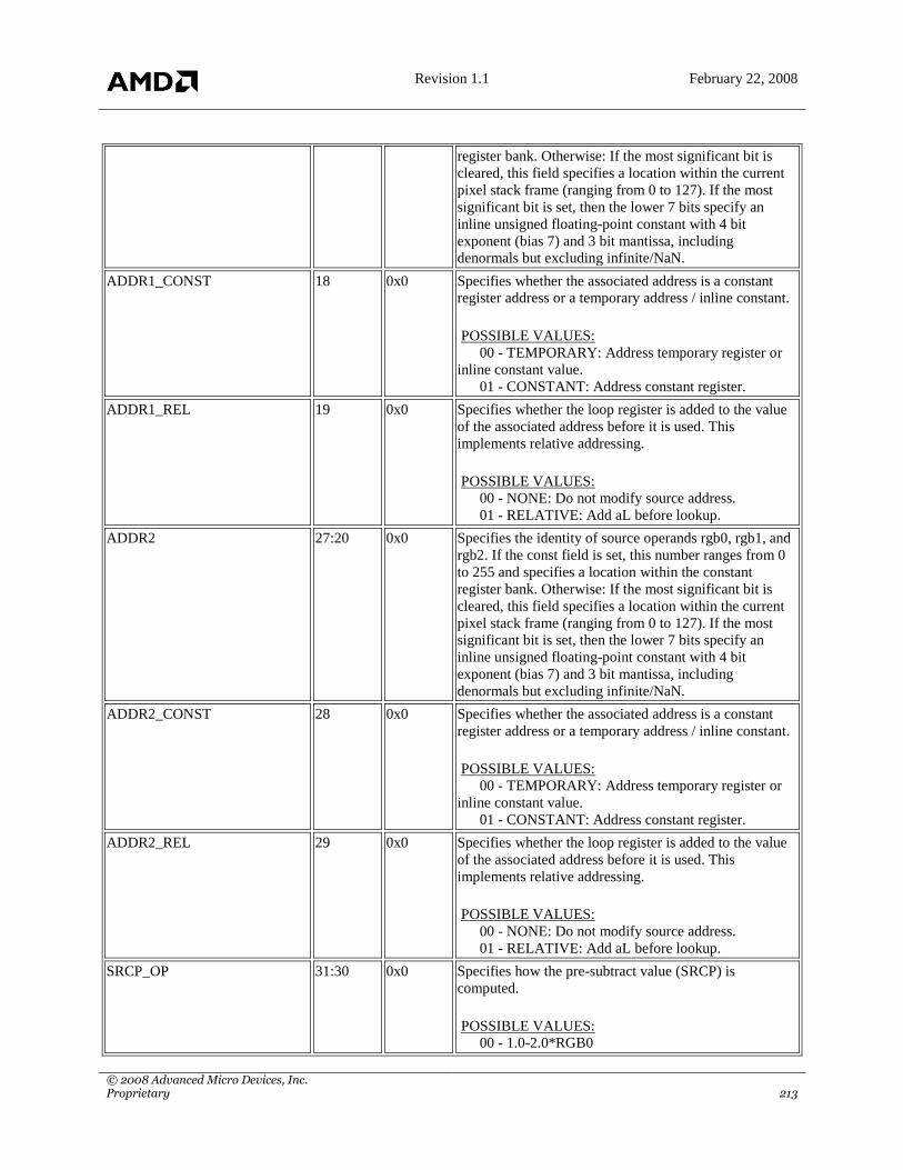
Revision 1.1 February 22, 2008
© 2008 Advanced Micro Devices, Inc. Proprietary 213
register bank. Otherwise: If the most significant bit is
cleared, this field specifies a location within the current
pixel stack frame (ranging from 0 to 127). If the most
significant bit is set, then the lower 7 bits specify an
inline unsigned floating-point constant with 4 bit
exponent (bias 7) and 3 bit mantissa, including
denormals but excluding infinite/NaN.
ADDR1_CONST 18 0x0 Specifies whether the associated address is a constant
register address or a temporary address / inline constant.
POSSIBLE VALUES:
00 - TEMPORARY: Address temporary register or
inline constant value.
01 - CONSTANT: Address constant register.
ADDR1_REL 19 0x0 Specifies whether the loop register is added to the value
of the associated address before it is used. This
implements relative addressing.
POSSIBLE VALUES:
00 - NONE: Do not modify source address.
01 - RELATIVE: Add aL before lookup.
ADDR2 27:20 0x0 Specifies the identity of source operands rgb0, rgb1, and
rgb2. If the const field is set, this number ranges from 0
to 255 and specifies a location within the constant
register bank. Otherwise: If the most significant bit is
cleared, this field specifies a location within the current
pixel stack frame (ranging from 0 to 127). If the most
significant bit is set, then the lower 7 bits specify an
inline unsigned floating-point constant with 4 bit
exponent (bias 7) and 3 bit mantissa, including
denormals but excluding infinite/NaN.
ADDR2_CONST 28 0x0 Specifies whether the associated address is a constant
register address or a temporary address / inline constant.
POSSIBLE VALUES:
00 - TEMPORARY: Address temporary register or
inline constant value.
01 - CONSTANT: Address constant register.
ADDR2_REL 29 0x0 Specifies whether the loop register is added to the value
of the associated address before it is used. This
implements relative addressing.
POSSIBLE VALUES:
00 - NONE: Do not modify source address.
01 - RELATIVE: Add aL before lookup.
SRCP_OP 31:30 0x0 Specifies how the pre-subtract value (SRCP) is
computed.
POSSIBLE VALUES:
00 - 1.0-2.0*RGB0
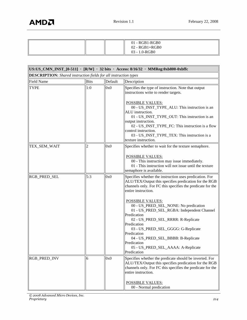
Revision 1.1 February 22, 2008
© 2008 Advanced Micro Devices, Inc. Proprietary 214
01 - RGB1-RGB0
02 - RGB1+RGB0
03 - 1.0-RGB0
US:US_CMN_INST_[0-511] · [R/W] · 32 bits · Access: 8/16/32 · MMReg:0xb800-0xbffc
DESCRIPTION: Shared instruction fields for all instruction types
Field Name Bits Default Description
TYPE 1:0 0x0 Specifies the type of instruction. Note that output
instructions write to render targets.
POSSIBLE VALUES:
00 - US_INST_TYPE_ALU: This instruction is an
ALU instruction.
01 - US_INST_TYPE_OUT: This instruction is an
output instruction.
02 - US_INST_TYPE_FC: This instruction is a flow
control instruction.
03 - US_INST_TYPE_TEX: This instruction is a
texture instruction.
TEX_SEM_WAIT 2 0x0 Specifies whether to wait for the texture semaphore.
POSSIBLE VALUES:
00 - This instruction may issue immediately.
01 - This instruction will not issue until the texture
semaphore is available.
RGB_PRED_SEL 5:3 0x0 Specifies whether the instruction uses predication. For
ALU/TEX/Output this specifies predication for the RGB
channels only. For FC this specifies the predicate for the
entire instruction.
POSSIBLE VALUES:
00 - US_PRED_SEL_NONE: No predication
01 - US_PRED_SEL_RGBA: Independent Channel
Predication
02 - US_PRED_SEL_RRRR: R-Replicate
Predication
03 - US_PRED_SEL_GGGG: G-Replicate
Predication
04 - US_PRED_SEL_BBBB: B-Replicate
Predication
05 - US_PRED_SEL_AAAA: A-Replicate
Predication
RGB_PRED_INV 6 0x0 Specifies whether the predicate should be inverted. For
ALU/TEX/Output this specifies predication for the RGB
channels only. For FC this specifies the predicate for the
entire instruction.
POSSIBLE VALUES:
00 - Normal predication
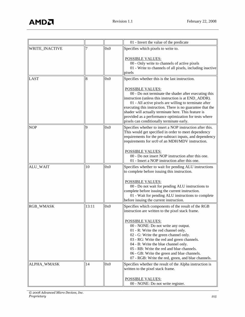
Revision 1.1 February 22, 2008
© 2008 Advanced Micro Devices, Inc. Proprietary 215
01 - Invert the value of the predicate
WRITE_INACTIVE 7 0x0 Specifies which pixels to write to.
POSSIBLE VALUES:
00 - Only write to channels of active pixels
01 - Write to channels of all pixels, including inactive
pixels
LAST 8 0x0 Specifies whether this is the last instruction.
POSSIBLE VALUES:
00 - Do not terminate the shader after executing this
instruction (unless this instruction is at END_ADDR).
01 - All active pixels are willing to terminate after
executing this instruction. There is no guarantee that the
shader will actually terminate here. This feature is
provided as a performance optimization for tests where
pixels can conditionally terminate early.
NOP 9 0x0 Specifies whether to insert a NOP instruction after this.
This would get specified in order to meet dependency
requirements for the pre-subtract inputs, and dependency
requirements for src0 of an MDH/MDV instruction.
POSSIBLE VALUES:
00 - Do not insert NOP instruction after this one.
01 - Insert a NOP instruction after this one.
ALU_WAIT 10 0x0 Specifies whether to wait for pending ALU instructions
to complete before issuing this instruction.
POSSIBLE VALUES:
00 - Do not wait for pending ALU instructions to
complete before issuing the current instruction.
01 - Wait for pending ALU instructions to complete
before issuing the current instruction.
RGB_WMASK 13:11 0x0 Specifies which components of the result of the RGB
instruction are written to the pixel stack frame.
POSSIBLE VALUES:
00 - NONE: Do not write any output.
01 - R: Write the red channel only.
02 - G: Write the green channel only.
03 - RG: Write the red and green channels.
04 - B: Write the blue channel only.
05 - RB: Write the red and blue channels.
06 - GB: Write the green and blue channels.
07 - RGB: Write the red, green, and blue channels.
ALPHA_WMASK 14 0x0 Specifies whether the result of the Alpha instruction is
written to the pixel stack frame.
POSSIBLE VALUES:
00 - NONE: Do not write register.

Revision 1.1 February 22, 2008
© 2008 Advanced Micro Devices, Inc. Proprietary 216
01 - A: Write the alpha channel only.
RGB_OMASK 17:15 0x0 Specifies which components of the result of the RGB
instruction are written to the output fifo if this is an
output instruction, and which predicate bits should be
modified if this is an ALU instruction.
POSSIBLE VALUES:
00 - NONE: Do not write any output.
01 - R: Write the red channel only.
02 - G: Write the green channel only.
03 - RG: Write the red and green channels.
04 - B: Write the blue channel only.
05 - RB: Write the red and blue channels.
06 - GB: Write the green and blue channels.
07 - RGB: Write the red, green, and blue channels.
ALPHA_OMASK 18 0x0 Specifies whether the result of the Alpha instruction is
written to the output fifo if this is an output instruction,
and whether the Alpha predicate bit should be modified
if this is an ALU instruction.
POSSIBLE VALUES:
00 - NONE: Do not write output.
01 - A: Write the alpha channel only.
RGB_CLAMP 19 0x0 Specifies RGB and Alpha clamp mode for this
instruction.
POSSIBLE VALUES:
00 - Do not clamp output.
01 - Clamp output to the range [0,1].
ALPHA_CLAMP 20 0x0 Specifies RGB and Alpha clamp mode for this
instruction.
POSSIBLE VALUES:
00 - Do not clamp output.
01 - Clamp output to the range [0,1].
ALU_RESULT_SEL 21 0x0 Specifies which component of the result of this
instruction should be used as the `ALU result` by a
subsequent flow control instruction.
POSSIBLE VALUES:
00 - RED: Use red as ALU result for FC.
01 - ALPHA: Use alpha as ALU result for FC.
ALPHA_PRED_INV 22 0x0 Specifies whether the predicate should be inverted. For
ALU/TEX/Output this specifies predication for the alpha
channel only. This field has no effect on FC instructions.
POSSIBLE VALUES:
00 - Normal predication
01 - Invert the value of the predicate

Revision 1.1 February 22, 2008
© 2008 Advanced Micro Devices, Inc. Proprietary 217
ALU_RESULT_OP 24:23 0x0 Specifies how to compare the ALU result against zero
for the `alu_result` bit in a subsequent flow control
instruction.
POSSIBLE VALUES:
00 - Equal to
01 - Less than
02 - Greater than or equal to
03 - Not equal
ALPHA_PRED_SEL 27:25 0x0 Specifies whether the instruction uses predication. For
ALU/TEX/Output this specifies predication for the alpha
channel only. This field has no effect on FC instructions.
POSSIBLE VALUES:
00 - US_PRED_SEL_NONE: No predication
01 - US_PRED_SEL_RGBA: A predication
(identical to US_PRED_SEL_AAAA)
02 - US_PRED_SEL_RRRR: R Predication
03 - US_PRED_SEL_GGGG: G Predication
04 - US_PRED_SEL_BBBB: B Predication
05 - US_PRED_SEL_AAAA: A Predication
STAT_WE 31:28 0x0 Specifies which components (R,G,B,A) contribute to the
stat count
US:US_CODE_ADDR · [R/W] · 32 bits · Access: 8/16/32 · MMReg:0x4630
DESCRIPTION: Code start and end instruction addresses.
Field Name Bits Default Description
START_ADDR 8:0 0x0 Specifies the address of the first instruction to execute in
the shader program. This address is relative to the shader
program offset given in
US_CODE_OFFSET.OFFSET_ADDR.
END_ADDR 24:16 0x0 Specifies the address of the last instruction to execute in
the shader program. This address is relative to the shader
program offset given in
US_CODE_OFFSET.OFFSET_ADDR. Shader program
execution will always terminate after the instruction at
this address is executed.
US:US_CODE_OFFSET · [R/W] · 32 bits · Access: 8/16/32 · MMReg:0x4638
DESCRIPTION: Offsets used for relative instruction addresses in the shader program, including START_ADDR,
END_ADDR, and any non-global flow control jump addresses.
Field Name Bits Default Description
OFFSET_ADDR 8:0 0x0 Specifies the offset to add to relative instruction
addresses, including START_ADDR, END_ADDR, and
some flow control jump addresses.
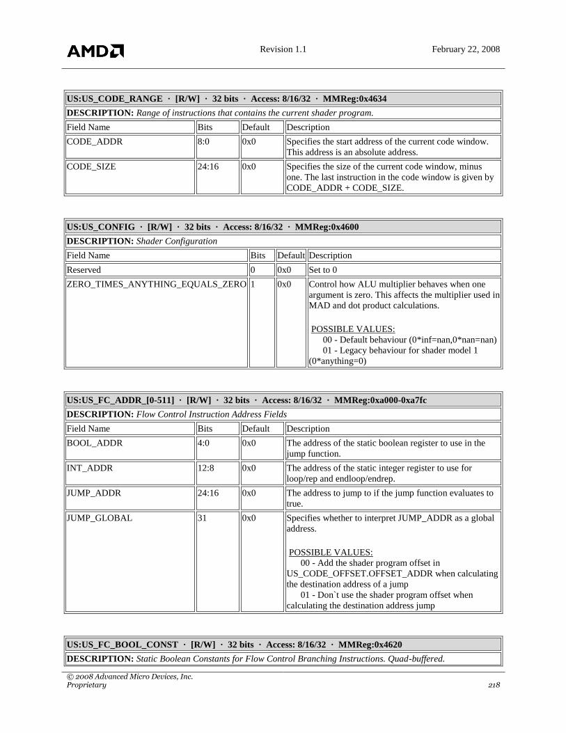
Revision 1.1 February 22, 2008
© 2008 Advanced Micro Devices, Inc. Proprietary 218
US:US_CODE_RANGE · [R/W] · 32 bits · Access: 8/16/32 · MMReg:0x4634
DESCRIPTION: Range of instructions that contains the current shader program.
Field Name Bits Default Description
CODE_ADDR 8:0 0x0 Specifies the start address of the current code window.
This address is an absolute address.
CODE_SIZE 24:16 0x0 Specifies the size of the current code window, minus
one. The last instruction in the code window is given by
CODE_ADDR + CODE_SIZE.
US:US_CONFIG · [R/W] · 32 bits · Access: 8/16/32 · MMReg:0x4600
DESCRIPTION: Shader Configuration
Field Name Bits Default Description
Reserved 0 0x0 Set to 0
ZERO_TIMES_ANYTHING_EQUALS_ZERO 1 0x0 Control how ALU multiplier behaves when one
argument is zero. This affects the multiplier used in
MAD and dot product calculations.
POSSIBLE VALUES:
00 - Default behaviour (0*inf=nan,0*nan=nan)
01 - Legacy behaviour for shader model 1
(0*anything=0)
US:US_FC_ADDR_[0-511] · [R/W] · 32 bits · Access: 8/16/32 · MMReg:0xa000-0xa7fc
DESCRIPTION: Flow Control Instruction Address Fields
Field Name Bits Default Description
BOOL_ADDR 4:0 0x0 The address of the static boolean register to use in the
jump function.
INT_ADDR 12:8 0x0 The address of the static integer register to use for
loop/rep and endloop/endrep.
JUMP_ADDR 24:16 0x0 The address to jump to if the jump function evaluates to
true.
JUMP_GLOBAL 31 0x0 Specifies whether to interpret JUMP_ADDR as a global
address.
POSSIBLE VALUES:
00 - Add the shader program offset in
US_CODE_OFFSET.OFFSET_ADDR when calculating
the destination address of a jump
01 - Don`t use the shader program offset when
calculating the destination address jump
US:US_FC_BOOL_CONST · [R/W] · 32 bits · Access: 8/16/32 · MMReg:0x4620
DESCRIPTION: Static Boolean Constants for Flow Control Branching Instructions. Quad-buffered.

Revision 1.1 February 22, 2008
© 2008 Advanced Micro Devices, Inc. Proprietary 219
Field Name Bits Default Description
KBOOL 31:0 0x0 Specifies the boolean value for constants 0-31.
US:US_FC_CTRL · [R/W] · 32 bits · Access: 8/16/32 · MMReg:0x4624
DESCRIPTION: Flow Control Options. Quad-buffered.
Field Name Bits Default Description
TEST_EN 30 0x0 Specifies whether test mode is enabled. This flag
currently has no effect in hardware.
POSSIBLE VALUES:
00 - Normal mode
01 - Test mode (currently unused)
FULL_FC_EN 31 0x0 Specifies whether full flow control functionality is
enabled.
POSSIBLE VALUES:
00 - Use partial flow-control (enables twice the
contexts). Loops and subroutines are not available in
partial flow-control mode, and the nesting depth of
branch statements is limited.
01 - Use full pixel shader 3.0 flow control, including
loops and subroutines.
US:US_FC_INST_[0-511] · [R/W] · 32 bits · Access: 8/16/32 · MMReg:0x9800-0x9ffc
DESCRIPTION: Flow Control Instruction
Field Name Bits Default Description
OP 2:0 0x0 Specifies the type of flow control instruction.
POSSIBLE VALUES:
00 - US_FC_OP_JUMP: (if, endif, call, etc)
01 - US_FC_OP_LOOP: same as jump except
always take the jump if the static counter is 0. If we don`t
take the jump, push initial loop counter and loop register
(aL) values onto the loop stack.
02 - US_FC_OP_ENDLOOP: same as jump but
decrement the loop counter and increment the loop
register (aL), and don`t take the jump if the loop counter
becomes zero.
03 - US_FC_OP_REP: same as loop but don`t push
the loop register aL.
04 - US_FC_OP_ENDREP: same as endloop but
don`t update/pop the loop register aL.
05 - US_FC_OP_BREAKLOOP: same as jump but
pops the loop stacks if a pixel stops being active.
06 - US_FC_OP_BREAKREP: same as breakloop
but don`t pop the loop register if it jumps.
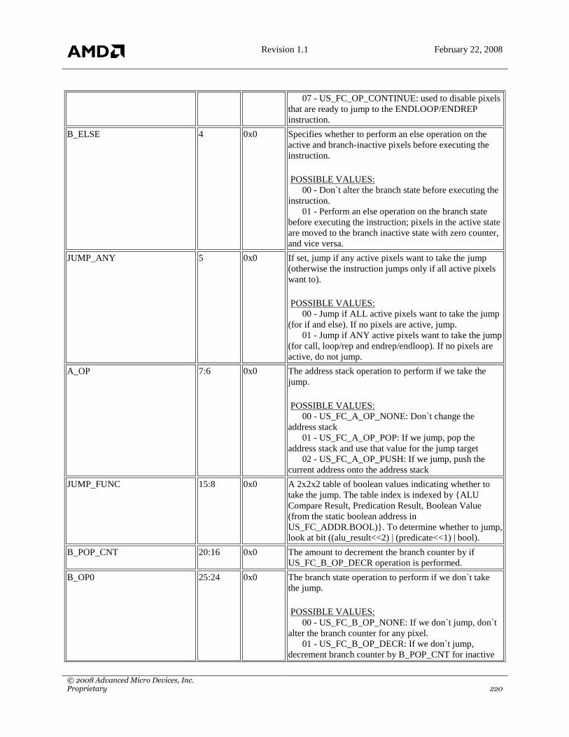
Revision 1.1 February 22, 2008
© 2008 Advanced Micro Devices, Inc. Proprietary 220
07 - US_FC_OP_CONTINUE: used to disable pixels
that are ready to jump to the ENDLOOP/ENDREP
instruction.
B_ELSE 4 0x0 Specifies whether to perform an else operation on the
active and branch-inactive pixels before executing the
instruction.
POSSIBLE VALUES:
00 - Don`t alter the branch state before executing the
instruction.
01 - Perform an else operation on the branch state
before executing the instruction; pixels in the active state
are moved to the branch inactive state with zero counter,
and vice versa.
JUMP_ANY 5 0x0 If set, jump if any active pixels want to take the jump
(otherwise the instruction jumps only if all active pixels
want to).
POSSIBLE VALUES:
00 - Jump if ALL active pixels want to take the jump
(for if and else). If no pixels are active, jump.
01 - Jump if ANY active pixels want to take the jump
(for call, loop/rep and endrep/endloop). If no pixels are
active, do not jump.
A_OP 7:6 0x0 The address stack operation to perform if we take the
jump.
POSSIBLE VALUES:
00 - US_FC_A_OP_NONE: Don`t change the
address stack
01 - US_FC_A_OP_POP: If we jump, pop the
address stack and use that value for the jump target
02 - US_FC_A_OP_PUSH: If we jump, push the
current address onto the address stack
JUMP_FUNC 15:8 0x0 A 2x2x2 table of boolean values indicating whether to
take the jump. The table index is indexed by {ALU
Compare Result, Predication Result, Boolean Value
(from the static boolean address in
US_FC_ADDR.BOOL)}. To determine whether to jump,
look at bit ((alu_result<<2) | (predicate<<1) | bool).
B_POP_CNT 20:16 0x0 The amount to decrement the branch counter by if
US_FC_B_OP_DECR operation is performed.
B_OP0 25:24 0x0 The branch state operation to perform if we don`t take
the jump.
POSSIBLE VALUES:
00 - US_FC_B_OP_NONE: If we don`t jump, don`t
alter the branch counter for any pixel.
01 - US_FC_B_OP_DECR: If we don`t jump,
decrement branch counter by B_POP_CNT for inactive

Revision 1.1 February 22, 2008
© 2008 Advanced Micro Devices, Inc. Proprietary 221
pixels. Activate pixels with negative counters.
02 - US_FC_B_OP_INCR: If we don`t jump,
increment branch counter by 1 for inactive pixels.
Deactivate pixels that decided to jump and set their
counter to zero.
B_OP1 27:26 0x0 The branch state operation to perform if we do take the
jump.
POSSIBLE VALUES:
00 - US_FC_B_OP_NONE: If we do jump, don`t
alter the branch counter for any pixel.
01 - US_FC_B_OP_DECR: If we do jump,
decrement branch counter by B_POP_CNT for inactive
pixels. Activate pixels with negative counters.
02 - US_FC_B_OP_INCR: If we do jump, increment
branch counter by 1 for inactive pixels. Deactivate pixels
that decided not to jump and set their counter to zero.
IGNORE_UNCOVERED 28 0x0 If set, uncovered pixels will not participate in flow
control decisions.
POSSIBLE VALUES:
00 - Include uncovered pixels in jump decisions
01 - Ignore uncovered pixels in making jump
decisions
US:US_FC_INT_CONST_[0-31] · [R/W] · 32 bits · Access: 8/16/32 · MMReg:0x4c00-0x4c7c
DESCRIPTION: Integer Constants used by Flow Control Loop Instructions. Single buffered.
Field Name Bits Default Description
KR 7:0 0x0 Specifies the number of iterations. Unsigned 8-bit integer
in [0, 255].
KG 15:8 0x0 Specifies the initial value of the loop register (aL).
Unsigned 8-bit integer in [0, 255].
KB 23:16 0x0 Specifies the increment used to change the loop register
(aL) on each iteration. Signed 7-bit integer in [-128,
127].
US:US_FORMAT0_[0-15] · [R/W] · 32 bits · Access: 8/16/32 · MMReg:0x4640-0x467c
Field Name Bits Default Description
TXWIDTH 10:0 0x0
TXHEIGHT 21:11 0x0
TXDEPTH 25:22 0x0 POSSIBLE VALUES:
13 - width > 2048, height <= 2048
14 - width <= 2048, height > 2048
15 - width > 2048, height > 2048

Revision 1.1 February 22, 2008
© 2008 Advanced Micro Devices, Inc. Proprietary 222
US:US_OUT_FMT_[0-3] · [R/W] · 32 bits · Access: 8/16/32 · MMReg:0x46a4-0x46b0
Field Name Bits Default Description
OUT_FMT 4:0 0x0 POSSIBLE VALUES:
00 - C4_8 (S/U)
01 - C4_10 (U)
02 - C4_10_GAMMA - (U)
03 - C_16 - (S/U)
04 - C2_16 - (S/U)
05 - C4_16 - (S/U)
06 - C_16_MPEG - (S)
07 - C2_16_MPEG - (S)
08 - C2_4 - (U)
09 - C_3_3_2 - (U)
10 - C_6_5_6 - (S/U)
11 - C_11_11_10 - (S/U)
12 - C_10_11_11 - (S/U)
13 - C_2_10_10_10 - (S/U)
14 - reserved
15 - UNUSED - Render target is not used
16 - C_16_FP - (S10E5)
17 - C2_16_FP - (S10E5)
18 - C4_16_FP - (S10E5)
19 - C_32_FP - (S23E8)
20 - C2_32_FP - (S23E8)
21 - C4_32_FP - (S23E8)
C0_SEL 9:8 0x0 POSSIBLE VALUES:
00 - Alpha
01 - Red
02 - Green
03 - Blue
C1_SEL 11:10 0x0 POSSIBLE VALUES:
00 - Alpha
01 - Red
02 - Green
03 - Blue
C2_SEL 13:12 0x0 POSSIBLE VALUES:
00 - Alpha
01 - Red
02 - Green
03 - Blue
C3_SEL 15:14 0x0 POSSIBLE VALUES:
00 - Alpha
01 - Red
02 - Green
03 - Blue
OUT_SIGN 19:16 0x0
ROUND_ADJ 20 0x0 POSSIBLE VALUES:
00 - Normal rounding
01 - Modified rounding of fixed-point data

Revision 1.1 February 22, 2008
© 2008 Advanced Micro Devices, Inc. Proprietary 223
US:US_PIXSIZE · [R/W] · 32 bits · Access: 8/16/32 · MMReg:0x4604
DESCRIPTION: Shader pixel size. This register specifies the size and partitioning of the current pixel stack frame
Field Name Bits Default Description
PIX_SIZE 6:0 0x0 Specifies the total size of the current pixel stack frame
(1:128)
US:US_TEX_ADDR_[0-511] · [R/W] · 32 bits · Access: 8/16/32 · MMReg:0x9800-0x9ffc
DESCRIPTION: Texture addresses and swizzles
Field Name Bits Default Description
SRC_ADDR 6:0 0x0 Specifies the location (within the shader pixel stack
frame) of the texture address for this instruction
SRC_ADDR_REL 7 0x0 Specifies whether the loop register is added to the value
of the associated address before it is used. This
implements relative addressing.
POSSIBLE VALUES:
00 - NONE: Do not modify source address
01 - RELATIVE: Add aL before lookup.
SRC_S_SWIZ 9:8 0x0 Specify which colour channel of src_addr to use for S
coordinate
POSSIBLE VALUES:
00 - Use R channel as S coordinate
01 - Use G channel as S coordinate
02 - Use B channel as S coordinate
03 - Use A channel as S coordinate
SRC_T_SWIZ 11:10 0x0 Specify which colour channel of src_addr to use for T
coordinate
POSSIBLE VALUES:
00 - Use R channel as T coordinate
01 - Use G channel as T coordinate
02 - Use B channel as T coordinate
03 - Use A channel as T coordinate
SRC_R_SWIZ 13:12 0x0 Specify which colour channel of src_addr to use for R
coordinate
POSSIBLE VALUES:
00 - Use R channel as R coordinate
01 - Use G channel as R coordinate
02 - Use B channel as R coordinate
03 - Use A channel as R coordinate
SRC_Q_SWIZ 15:14 0x0 Specify which colour channel of src_addr to use for Q
coordinate
POSSIBLE VALUES:
00 - Use R channel as Q coordinate

Revision 1.1 February 22, 2008
© 2008 Advanced Micro Devices, Inc. Proprietary 224
01 - Use G channel as Q coordinate
02 - Use B channel as Q coordinate
03 - Use A channel as Q coordinate
DST_ADDR 22:16 0x0 Specifies the location (within the shader pixel stack
frame) of the returned texture data for this instruction
DST_ADDR_REL 23 0x0 Specifies whether the loop register is added to the value
of the associated address before it is used. This
implements relative addressing.
POSSIBLE VALUES:
00 - NONE: Do not modify destination address
01 - RELATIVE: Add aL before lookup.
DST_R_SWIZ 25:24 0x0 Specify which colour channel of the returned texture data
to write to the red channel of dst_addr
POSSIBLE VALUES:
00 - Write R channel to R channel
01 - Write G channel to R channel
02 - Write B channel to R channel
03 - Write A channel to R channel
DST_G_SWIZ 27:26 0x0 Specify which colour channel of the returned texture data
to write to the green channel of dst_addr
POSSIBLE VALUES:
00 - Write R channel to G channel
01 - Write G channel to G channel
02 - Write B channel to G channel
03 - Write A channel to G channel
DST_B_SWIZ 29:28 0x0 Specify which colour channel of the returned texture data
to write to the blue channel of dst_addr
POSSIBLE VALUES:
00 - Write R channel to B channel
01 - Write G channel to B channel
02 - Write B channel to B channel
03 - Write A channel to B channel
DST_A_SWIZ 31:30 0x0 Specify which colour channel of the returned texture data
to write to the alpha channel of dst_addr
POSSIBLE VALUES:
00 - Write R channel to A channel
01 - Write G channel to A channel
02 - Write B channel to A channel
03 - Write A channel to A channel
US:US_TEX_ADDR_DXDY_[0-511] · [R/W] · 32 bits · Access: 8/16/32 · MMReg:0xa000-0xa7fc
DESCRIPTION: Additional texture addresses and swizzles for DX/DY inputs
Field Name Bits Default Description

Revision 1.1 February 22, 2008
© 2008 Advanced Micro Devices, Inc. Proprietary 225
DX_ADDR 6:0 0x0 Specifies the location (within the shader pixel stack
frame) of the DX value for this instruction
DX_ADDR_REL 7 0x0 Specifies whether the loop register is added to the value
of the associated address before it is used. This
implements relative addressing.
POSSIBLE VALUES:
00 - NONE: Do not modify source address
01 - RELATIVE: Add aL before lookup.
DX_S_SWIZ 9:8 0x0 Specify which colour channel of dx_addr to use for S
coordinate
POSSIBLE VALUES:
00 - Use R channel as S coordinate
01 - Use G channel as S coordinate
02 - Use B channel as S coordinate
03 - Use A channel as S coordinate
DX_T_SWIZ 11:10 0x0 Specify which colour channel of dx_addr to use for T
coordinate
POSSIBLE VALUES:
00 - Use R channel as T coordinate
01 - Use G channel as T coordinate
02 - Use B channel as T coordinate
03 - Use A channel as T coordinate
DX_R_SWIZ 13:12 0x0 Specify which colour channel of dx_addr to use for R
coordinate
POSSIBLE VALUES:
00 - Use R channel as R coordinate
01 - Use G channel as R coordinate
02 - Use B channel as R coordinate
03 - Use A channel as R coordinate
DX_Q_SWIZ 15:14 0x0 Specify which colour channel of dx_addr to use for Q
coordinate
POSSIBLE VALUES:
00 - Use R channel as Q coordinate
01 - Use G channel as Q coordinate
02 - Use B channel as Q coordinate
03 - Use A channel as Q coordinate
DY_ADDR 22:16 0x0 Specifies the location (within the shader pixel stack
frame) of the DY value for this instruction
DY_ADDR_REL 23 0x0 Specifies whether the loop register is added to the value
of the associated address before it is used. This
implements relative addressing.
POSSIBLE VALUES:
00 - NONE: Do not modify source address

Revision 1.1 February 22, 2008
© 2008 Advanced Micro Devices, Inc. Proprietary 226
01 - RELATIVE: Add aL before lookup.
DY_S_SWIZ 25:24 0x0 Specify which colour channel of dy_addr to use for S
coordinate
POSSIBLE VALUES:
00 - Use R channel as S coordinate
01 - Use G channel as S coordinate
02 - Use B channel as S coordinate
03 - Use A channel as S coordinate
DY_T_SWIZ 27:26 0x0 Specify which colour channel of dy_addr to use for T
coordinate
POSSIBLE VALUES:
00 - Use R channel as T coordinate
01 - Use G channel as T coordinate
02 - Use B channel as T coordinate
03 - Use A channel as T coordinate
DY_R_SWIZ 29:28 0x0 Specify which colour channel of dy_addr to use for R
coordinate
POSSIBLE VALUES:
00 - Use R channel as R coordinate
01 - Use G channel as R coordinate
02 - Use B channel as R coordinate
03 - Use A channel as R coordinate
DY_Q_SWIZ 31:30 0x0 Specify which colour channel of dy_addr to use for Q
coordinate
POSSIBLE VALUES:
00 - Use R channel as Q coordinate
01 - Use G channel as Q coordinate
02 - Use B channel as Q coordinate
03 - Use A channel as Q coordinate
US:US_TEX_INST_[0-511] · [R/W] · 32 bits · Access: 8/16/32 · MMReg:0x9000-0x97fc
DESCRIPTION: Texture Instruction
Field Name Bits Default Description
TEX_ID 19:16 0x0 Specifies the id of the texture map used for this
instruction
INST 24:22 0x0 Specifies the operation taking place for this instruction
POSSIBLE VALUES:
00 - NOP: Do nothing
01 - LD: Do Texture Lookup (S,T,R)
02 - TEXKILL: Kill pixel if any component is < 0
03 - PROJ: Do projected texture lookup
(S/Q,T/Q,R/Q)
04 - LODBIAS: Do texture lookup with lod bias

Revision 1.1 February 22, 2008
© 2008 Advanced Micro Devices, Inc. Proprietary 227
05 - LOD: Do texture lookup with explicit lod
06 - DXDY: Do texture lookup with lod calculated
from DX and DY
TEX_SEM_ACQUIRE 25 0x0 Whether to hold the texture semaphore until the data is
written to the temporary register.
POSSIBLE VALUES:
00 - Don`t hold the texture semaphore
01 - Hold the texture semaphore until the data is
written to the temporary register.
IGNORE_UNCOVERED 26 0x0 If set, US will not request data for pixels which are
uncovered. Clear this bit for indirect texture lookups.
POSSIBLE VALUES:
00 - Fetch texels for uncovered pixels
01 - Don`t fetch texels for uncovered pixels
UNSCALED 27 0x0 Whether to scale texture coordinates when sending them
to the texture unit.
POSSIBLE VALUES:
00 - Scale the S, T, R texture coordinates from
[0.0,1.0] to the dimensions of the target texture
01 - Use the unscaled S, T, R texture coordates.
US:US_W_FMT · [R/W] · 32 bits · Access: 8/16/32 · MMReg:0x46b4
DESCRIPTION: Specifies the source and format for the Depth (W) value output by the shader
Field Name Bits Default Description
W_FMT 1:0 0x0 Format for W
POSSIBLE VALUES:
00 - W0 - W is always zero
01 - W24 - 24-bit fixed point
02 - W24_FP - 24-bit floating point. The floating
point values are a special format that preserve sorting
order when values are compared as integers, allowing
higher precision in W without additional logic in other
blocks.
03 - Reserved
W_SRC 2 0x0 Source for W
POSSIBLE VALUES:
00 - WSRC_US - W comes from shader instruction
01 - WSRC_RAS - W comes from rasterizer

Revision 1.1 February 22, 2008
© 2008 Advanced Micro Devices, Inc. Proprietary 228
10.10 Vertex Registers
VAP:VAP_ALT_NUM_VERTICES · [R/W] · 32 bits · Access: 32 · MMReg:0x2088
DESCRIPTION: Alternate Number of Vertices to allow > 16-bits of Vertex count
Field Name Bits Default Description
NUM_VERTICES 23:0 0x0 24-bit vertex count for command packet. Used instead of
bits 31:16 of VAP_VF_CNTL if
VAP_VF_CNTL.USE_ALT_NUM_VERTS is set.
VAP:VAP_CLIP_CNTL · [R/W] · 32 bits · Access: 32 · MMReg:0x221c
DESCRIPTION: Control Bits for User Clip Planes and Clipping
Field Name Bits Default Description
UCP_ENA_0 0 0x0 Enable User Clip Plane 0
UCP_ENA_1 1 0x0 Enable User Clip Plane 1
UCP_ENA_2 2 0x0 Enable User Clip Plane 2
UCP_ENA_3 3 0x0 Enable User Clip Plane 3
UCP_ENA_4 4 0x0 Enable User Clip Plane 4
UCP_ENA_5 5 0x0 Enable User Clip Plane 5
PS_UCP_MODE 15:14 0x0 0 = Cull using distance from center of point
1 = Cull using radius-based distance from center of
point
2 = Cull using radius-based distance from center of
point, Expand and Clip on intersection
3 = Always expand and clip as trifan
CLIP_DISABLE 16 0x0 Disables clip code generation and clipping process for
TCL
UCP_CULL_ONLY_ENA 17 0x0 Cull Primitives against UCPS, but don`t clip
BOUNDARY_EDGE_FLAG_ENA 18 0x0 If set, boundary edges are highlighted, else they are not
highlighted
COLOR2_IS_TEXTURE 20 0x0 If set, color2 is used as texture8 by GA (PS3.0
requirement)
COLOR3_IS_TEXTURE 21 0x0 If set, color3 is used as texture9 by GA (PS3.0
requirement)
VAP:VAP_CNTL · [R/W] · 32 bits · Access: 32 · MMReg:0x2080
DESCRIPTION: Vertex Assembler/Processor Control Register
Field Name Bits Default Description
PVS_NUM_SLOTS 3:0 0x0 Specifies the number of vertex slots to be used in the
VAP PVS process. A slot represents a single vertex
storage location1 across multiple engines (one vertex per
engine). By decreasing the number of slots, there is more
memory for each vertex, but less parallel processing.

Revision 1.1 February 22, 2008
© 2008 Advanced Micro Devices, Inc. Proprietary 229
Similarly, by increasing the number of slots, there is less
memory per vertex but more vertices being processed in
parallel.
PVS_NUM_CNTLRS 7:4 0x0 Specifies the maximum number of controllers to be
processing in parallel. In general should be set to max
value of TBD. Can be changed for performance analysis.
PVS_NUM_FPUS 11:8 0x0 Specifies the number of Floating Point Units
(Vector/Math Engines) to use when processing vertices.
VAP_NO_RENDER 17 0x0 If set, VAP will not process any draw commands (i.e.
writes to VAP_VF_CNTL, the INDX and DATAPORT
and Immediate mode writes are ignored.
VF_MAX_VTX_NUM 21:18 0x9 This field controls the number of vertices that the vertex
fetcher manages for the TCL and Setup Vertex Storage
memories (and therefore the number of vertices that can
be re-used). This value should be set to 12 for most
operation, This number may be modified for
performance evaluation. The value is the maximum
vertex number used which is one less than the number of
vertices (i.e. a 12 means 13 vertices will be used)
DX_CLIP_SPACE_DEF 22 0x0 Clip space is defined as:
0: -W < X < W, -W < Y < W, -W < Z < W (OpenGL
Definition)
1: -W < X < W, -W < Y < W, 0 < Z < W (DirectX
Definition)
TCL_STATE_OPTIMIZATION 23 0x0 If set, enables the TCL state optimization, and the new
state is used only if there is a change in TCL state,
between VF_CNTL (triggers)
VAP:VAP_CNTL_STATUS · [R/W] · 32 bits · Access: 32 · MMReg:0x2140
DESCRIPTION: Vertex Assemblen/Processor Control Status
Field Name Bits Default Description
VC_SWAP 1:0 0x0 Endian-Swap Control.
0 = No swap 1 = 16-bit swap: 0xAABBCCDD becomes
0xBBAADDCC
2 = 32-bit swap: 0xAABBCCDD becomes
0xDDCCBBAA
3 = Half-dword swap: 0xAABBCCDD becomes
0xCCDDAABB
Default = 0
PVS_BYPASS 8 0x0 The TCL engine is logically or physically removed from
the circuit.
PVS_BUSY
(Access: R)
11 0x0 Transform/Clip/Light (TCL) Engine is Busy. Read-only.
MAX_MPS
(Access: R)
19:16 0x0 Maximum number of MPs fused for this chip. Read-
only.
For A11, fusemask is fixed to 1XXX.
For A12,

Revision 1.1 February 22, 2008
© 2008 Advanced Micro Devices, Inc. Proprietary 230
CG.CC_COMBINEDSTRAPS.MAX_MPS[7:5] = 000
=> max_mps[3:0] = 1XXX => 8 MPs
CG.CC_COMBINEDSTRAPS.MAX_MPS[7:5] = 001
=> max_mps[3:0] = 0110 => 6 MPs
CG.CC_COMBINEDSTRAPS.MAX_MPS[7:5] = 010
=> max_mps[3:0] = 0101 => 5 MPs
CG.CC_COMBINEDSTRAPS.MAX_MPS[7:5] = 011
=> max_mps[3:0] = 0100 => 4 MPs
CG.CC_COMBINEDSTRAPS.MAX_MPS[7:5] = 100
=> max_mps[3:0] = 0011 => 3 MPs
CG.CC_COMBINEDSTRAPS.MAX_MPS[7:5] = 101
=> max_mps[3:0] = 0010 => 2 MPs
CG.CC_COMBINEDSTRAPS.MAX_MPS[7:5] = 110
=> max_mps[3:0] = 0001 => 1 MP
CG.CC_COMBINEDSTRAPS.MAX_MPS[7:5] = 111
=> max_mps[3:0] = 0000 => 0 MP
Note that max_mps[3:0] = 0111 = 7 MPs is not available
VS_BUSY
(Access: R)
24 0x0 Vertex Store is Busy. Read-only.
RCP_BUSY
(Access: R)
25 0x0 Reciprocal Engine is Busy. Read-only.
VTE_BUSY
(Access: R)
26 0x0 ViewPort Transform Engine is Busy. Read-only.
MIU_BUSY
(Access: R)
27 0x0 Memory Interface Unit is Busy. Read-only.
VC_BUSY
(Access: R)
28 0x0 Vertex Cache is Busy. Read-only.
VF_BUSY
(Access: R)
29 0x0 Vertex Fetcher is Busy. Read-only.
REGPIPE_BUSY
(Access: R)
30 0x0 Register Pipeline is Busy. Read-only.
VAP_BUSY
(Access: R)
31 0x0 VAP Engine is Busy. Read-only.
VAP:VAP_GB_HORZ_CLIP_ADJ · [R/W] · 32 bits · Access: 32 · MMReg:0x2228
DESCRIPTION: Horizontal Guard Band Clip Adjust Register
Field Name Bits Default Description
DATA_REGISTER 31:0 0x0 32-bit floating point value. Should be set to 1.0 for no
guard band.
VAP:VAP_GB_HORZ_DISC_ADJ · [R/W] · 32 bits · Access: 32 · MMReg:0x222c
DESCRIPTION: Horizontal Guard Band Discard Adjust Register
Field Name Bits Default Description
DATA_REGISTER 31:0 0x0 32-bit floating point value. Should be set to 1.0 for no
guard band.
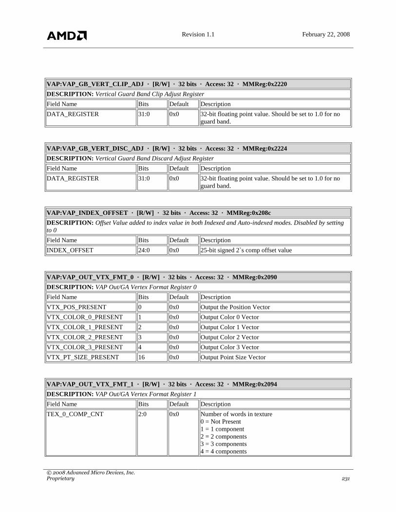
Revision 1.1 February 22, 2008
© 2008 Advanced Micro Devices, Inc. Proprietary 231
VAP:VAP_GB_VERT_CLIP_ADJ · [R/W] · 32 bits · Access: 32 · MMReg:0x2220
DESCRIPTION: Vertical Guard Band Clip Adjust Register
Field Name Bits Default Description
DATA_REGISTER 31:0 0x0 32-bit floating point value. Should be set to 1.0 for no
guard band.
VAP:VAP_GB_VERT_DISC_ADJ · [R/W] · 32 bits · Access: 32 · MMReg:0x2224
DESCRIPTION: Vertical Guard Band Discard Adjust Register
Field Name Bits Default Description
DATA_REGISTER 31:0 0x0 32-bit floating point value. Should be set to 1.0 for no
guard band.
VAP:VAP_INDEX_OFFSET · [R/W] · 32 bits · Access: 32 · MMReg:0x208c
DESCRIPTION: Offset Value added to index value in both Indexed and Auto-indexed modes. Disabled by setting
to 0
Field Name Bits Default Description
INDEX_OFFSET 24:0 0x0 25-bit signed 2`s comp offset value
VAP:VAP_OUT_VTX_FMT_0 · [R/W] · 32 bits · Access: 32 · MMReg:0x2090
DESCRIPTION: VAP Out/GA Vertex Format Register 0
Field Name Bits Default Description
VTX_POS_PRESENT 0 0x0 Output the Position Vector
VTX_COLOR_0_PRESENT 1 0x0 Output Color 0 Vector
VTX_COLOR_1_PRESENT 2 0x0 Output Color 1 Vector
VTX_COLOR_2_PRESENT 3 0x0 Output Color 2 Vector
VTX_COLOR_3_PRESENT 4 0x0 Output Color 3 Vector
VTX_PT_SIZE_PRESENT 16 0x0 Output Point Size Vector
VAP:VAP_OUT_VTX_FMT_1 · [R/W] · 32 bits · Access: 32 · MMReg:0x2094
DESCRIPTION: VAP Out/GA Vertex Format Register 1
Field Name Bits Default Description
TEX_0_COMP_CNT 2:0 0x0 Number of words in texture
0 = Not Present
1 = 1 component
2 = 2 components
3 = 3 components
4 = 4 components

Revision 1.1 February 22, 2008
© 2008 Advanced Micro Devices, Inc. Proprietary 232
TEX_1_COMP_CNT 5:3 0x0 Number of words in texture
0 = Not Present
1 = 1 component
2 = 2 components
3 = 3 components
4 = 4 components
TEX_2_COMP_CNT 8:6 0x0 Number of words in texture
0 = Not Present
1 = 1 component
2 = 2 components
3 = 3 components
4 = 4 components
TEX_3_COMP_CNT 11:9 0x0 Number of words in texture
0 = Not Present
1 = 1 component
2 = 2 components
3 = 3 components
4 = 4 components
TEX_4_COMP_CNT 14:12 0x0 Number of words in texture
0 = Not Present
1 = 1 component
2 = 2 components
3 = 3 components
4 = 4 components
TEX_5_COMP_CNT 17:15 0x0 Number of words in texture
0 = Not Present
1 = 1 component
2 = 2 components
3 = 3 components
4 = 4 components
TEX_6_COMP_CNT 20:18 0x0 Number of words in texture
0 = Not Present
1 = 1 component
2 = 2 components
3 = 3 components
4 = 4 components
TEX_7_COMP_CNT 23:21 0x0 Number of words in texture
0 = Not Present
1 = 1 component
2 = 2 components
3 = 3 components
4 = 4 components
VAP:VAP_PORT_DATA[0-15] · [W] · 32 bits · Access: 32 · MMReg:0x2000-0x203c
DESCRIPTION: Setup Engine Data Port 0 through 15.
Field Name Bits Default Description
DATAPORT0
(master with mirrors)
31:0 0x0 1st of 16 consecutive dwords for writing vertex data
information.

Revision 1.1 February 22, 2008
© 2008 Advanced Micro Devices, Inc. Proprietary 233
Write-only.
VAP:VAP_PORT_DATA_IDX_128 · [W] · 32 bits · Access: 32 · MMReg:0x20b8
DESCRIPTION: 128-bit Data Port for Indexed Primitives.
Field Name Bits Default Description
DATA_IDX_PORT_128 31:0 0x0 128-bit Data Port for Indexed Primitives.
Write-only.
VAP:VAP_PORT_IDX[0-15] · [W] · 32 bits · Access: 32 · MMReg:0x2040-0x207c
DESCRIPTION: Setup Engine Index Port 0 through 15.
Field Name Bits Default Description
IDXPORT0
(master with mirrors)
31:0 0x0 1st of 16 consecutive dwords for writing vertex index
information, in the format of:
15:0 Index 0
31:16 Index 1
Write-only.
VAP:VAP_PROG_STREAM_CNTL_[0-7] · [R/W] · 32 bits · Access: 32 · MMReg:0x2150-0x216c
DESCRIPTION: Programmable Stream Control Word 0
Field Name Bits Default Description
DATA_TYPE_0 3:0 0x0 The data type for element 0
0 = FLOAT_1 (Single IEEE Float)
1 = FLOAT_2 (2 IEEE floats)
2 = FLOAT_3 (3 IEEE Floats)
3 = FLOAT_4 (4 IEEE Floats)
4 = BYTE * (1 DWORD w 4 8-bit fixed point values)
(X = [7:0], Y = [15:8], Z = [23:16], W = [31:24])
5 = D3DCOLOR * (Same as BYTE except has X->Z,Z-
>X swap for D3D color def)
(Z = [7:0], Y = [15:8], X = [23:16], W = [31:24])
6 = SHORT_2 * (1 DWORD with 2 16-bit fixed point
values)
(X = [15:0], Y = [31:16], Z = 0.0, W = 1.0)
7 = SHORT_4 * (2 DWORDS with 4(2 per dword) 16-
bit fixed point values)
(X = DW0 [15:0], Y = DW0 [31:16], Z = DW1 [15:0],
W = DW1 [31:16])
8 = VECTOR_3_TTT * (1 DWORD with 3 10-bit fixed
point values)
(X = [9:0], Y = [19:10], Z = [29:20], W = 1.0)
9 = VECTOR_3_EET * (1 DWORD with 2 11-bit and 1
10-bit fixed point values)
(X = [10:0], Y = [21:11], Z = [31:22], W = 1.0)
10 = FLOAT_8 (8 IEEE Floats)
Sames as 2 FLOAT_4 but must use consecutive

Revision 1.1 February 22, 2008
© 2008 Advanced Micro Devices, Inc. Proprietary 234
DST_VEC_LOC. Used to allow > 16 PSC for OGL path.
11 = FLT16_2 (1 DWORD with 2 16-bit floating point
values (SE5M10 exp bias of 15, supports denormalized
numbers))
(X = [15:0], Y = [31:16], Z = 0.0, W = 1.0)
12 = FLT16_4 (2 DWORDS with 4(2 per dword) 16-bit
floating point values (SE5M10 exp bias of 15, supports
denormalized numbers)))
(X = DW0 [15:0], Y = DW0 [31:16], Z = DW1 [15:0],
W = DW1 [31:16])
* These data types use the SIGNED and NORMALIZE
flags described below.
SKIP_DWORDS_0 7:4 0x0 The number of DWORDS to skip (discard) after
processing the current element.
DST_VEC_LOC_0 12:8 0x0 The vector address in the input memory to write this
element
LAST_VEC_0 13 0x0 If set, indicates the last vector of the current vertex
stream
SIGNED_0 14 0x0 Determines whether fixed point data types are unsigned
(0) or 2`s complement signed (1) data types. See
NORMALIZE for complete description of affect
NORMALIZE_0 15 0x0 Determines whether the fixed to floating point
conversion will normalize the value (i.e. fixed point
value is all fractional bits) or not (i.e. fixed point value is
all integer bits).
This table describes the fixed to float conversion results
SIGNED NORMALIZE FLT RANGE
0 0 0.0 - (2^n - 1) (i.e. 8-bit -> 0.0 - 255.0)
0 1 0.0 - 1.0
1 0 -2^(n-1) - (2^(n-1) - 1) (i.e. 8-bit -> -128.0 - 127.0)
1 1 -1.0 - 1.0
where n is the number of bits in the associated fixed
point value
For signed, normalize conversion, since the fixed point
range is not evenly distributed around 0, there are 3
different methods supported by R300. See the
VAP_PSC_SGN_NORM_CNTL description for details.
DATA_TYPE_1 19:16 0x0 Similar to DATA_TYPE_0
SKIP_DWORDS_1 23:20 0x0 See SKIP_DWORDS_0
DST_VEC_LOC_1 28:24 0x0 See DST_VEC_LOC_0
LAST_VEC_1 29 0x0 See LAST_VEC_0
SIGNED_1 30 0x0 See SIGNED_0
NORMALIZE_1 31 0x0 See NORMALIZE_0
VAP:VAP_PROG_STREAM_CNTL_EXT_[0-7] · [R/W] · 32 bits · Access: 32 · MMReg:0x21e0-0x21fc
DESCRIPTION: Programmable Stream Control Extension Word 0
Field Name Bits Default Description

Revision 1.1 February 22, 2008
© 2008 Advanced Micro Devices, Inc. Proprietary 235
SWIZZLE_SELECT_X_0 2:0 0x0 X-Component Swizzle Select
0 = SELECT_X
1 = SELECT_Y
2 = SELECT_Z
3 = SELECT_W
4 = SELECT_FP_ZERO (Floating Point 0.0)
5 = SELECT_FP_ONE (Floating Point 1.0)
6,7 RESERVED
SWIZZLE_SELECT_Y_0 5:3 0x0 Y-Component Swizzle Select (See Above)
SWIZZLE_SELECT_Z_0 8:6 0x0 Z-Component Swizzle Select (See Above)
SWIZZLE_SELECT_W_0 11:9 0x0 W-Component Swizzle Select (See Above)
WRITE_ENA_0 15:12 0x0 4-bit write enable.
Bit 0 maps to X
Bit 1 maps to Y
Bit 2 maps to Z
Bit 3 maps to W
SWIZZLE_SELECT_X_1 18:16 0x0 See SWIZZLE_SELECT_X_0
SWIZZLE_SELECT_Y_1 21:19 0x0 See SWIZZLE_SELECT_Y_0
SWIZZLE_SELECT_Z_1 24:22 0x0 See SWIZZLE_SELECT_Z_0
SWIZZLE_SELECT_W_1 27:25 0x0 See SWIZZLE_SELECT_W_0
WRITE_ENA_1 31:28 0x0 See WRITE_ENA_0
VAP:VAP_PSC_SGN_NORM_CNTL · [R/W] · 32 bits · Access: 32 · MMReg:0x21dc
DESCRIPTION: Programmable Stream Control Signed Normalize Control
Field Name Bits Default Description
SGN_NORM_METHOD_0 1:0 0x0 There are 3 methods of normalizing signed numbers:
0: SGN_NORM_ZERO : value / (2^(n-1)-1), so -
128/127 will be less that -1.0, -127/127 will yeild -1.0,
0/127 will yield 0, and 127/127 will yield 1.0 for 8-bit
numbers.
1: SGN_NORM_ZERO_CLAMP_MINUS_ONE: Same
as SGN_NORM_ZERO except -128/127 will yield -1.0
for 8-bit numbers.
2: SGN_NORM_NO_ZERO: (2 * value + 1)/2^n, so -
128 will yield -255/255 = -1.0, 127 will yield 255/255 =
1.0, but 0 will yield 1/255 != 0.
SGN_NORM_METHOD_1 3:2 0x0 See SGN_NORM_METHOD_0
SGN_NORM_METHOD_2 5:4 0x0 See SGN_NORM_METHOD_0
SGN_NORM_METHOD_3 7:6 0x0 See SGN_NORM_METHOD_0
SGN_NORM_METHOD_4 9:8 0x0 See SGN_NORM_METHOD_0
SGN_NORM_METHOD_5 11:10 0x0 See SGN_NORM_METHOD_0
SGN_NORM_METHOD_6 13:12 0x0 See SGN_NORM_METHOD_0
SGN_NORM_METHOD_7 15:14 0x0 See SGN_NORM_METHOD_0
SGN_NORM_METHOD_8 17:16 0x0 See SGN_NORM_METHOD_0
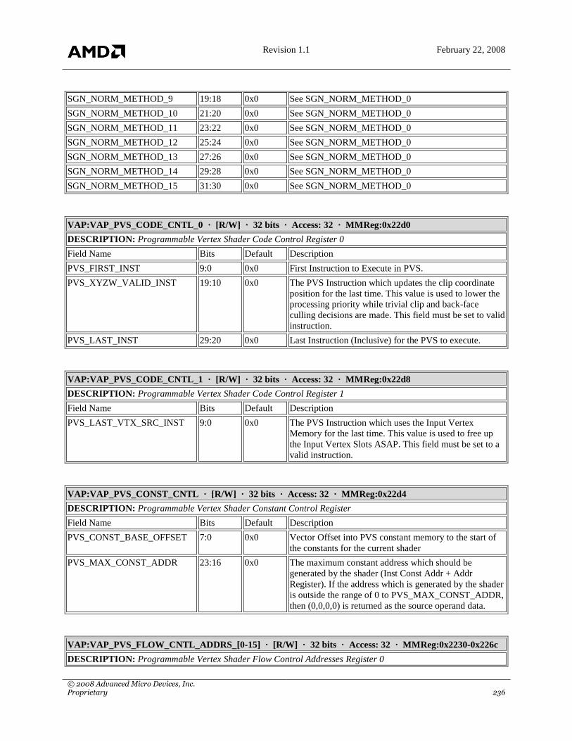
Revision 1.1 February 22, 2008
© 2008 Advanced Micro Devices, Inc. Proprietary 236
SGN_NORM_METHOD_9 19:18 0x0 See SGN_NORM_METHOD_0
SGN_NORM_METHOD_10 21:20 0x0 See SGN_NORM_METHOD_0
SGN_NORM_METHOD_11 23:22 0x0 See SGN_NORM_METHOD_0
SGN_NORM_METHOD_12 25:24 0x0 See SGN_NORM_METHOD_0
SGN_NORM_METHOD_13 27:26 0x0 See SGN_NORM_METHOD_0
SGN_NORM_METHOD_14 29:28 0x0 See SGN_NORM_METHOD_0
SGN_NORM_METHOD_15 31:30 0x0 See SGN_NORM_METHOD_0
VAP:VAP_PVS_CODE_CNTL_0 · [R/W] · 32 bits · Access: 32 · MMReg:0x22d0
DESCRIPTION: Programmable Vertex Shader Code Control Register 0
Field Name Bits Default Description
PVS_FIRST_INST 9:0 0x0 First Instruction to Execute in PVS.
PVS_XYZW_VALID_INST 19:10 0x0 The PVS Instruction which updates the clip coordinate
position for the last time. This value is used to lower the
processing priority while trivial clip and back-face
culling decisions are made. This field must be set to valid
instruction.
PVS_LAST_INST 29:20 0x0 Last Instruction (Inclusive) for the PVS to execute.
VAP:VAP_PVS_CODE_CNTL_1 · [R/W] · 32 bits · Access: 32 · MMReg:0x22d8
DESCRIPTION: Programmable Vertex Shader Code Control Register 1
Field Name Bits Default Description
PVS_LAST_VTX_SRC_INST 9:0 0x0 The PVS Instruction which uses the Input Vertex
Memory for the last time. This value is used to free up
the Input Vertex Slots ASAP. This field must be set to a
valid instruction.
VAP:VAP_PVS_CONST_CNTL · [R/W] · 32 bits · Access: 32 · MMReg:0x22d4
DESCRIPTION: Programmable Vertex Shader Constant Control Register
Field Name Bits Default Description
PVS_CONST_BASE_OFFSET 7:0 0x0 Vector Offset into PVS constant memory to the start of
the constants for the current shader
PVS_MAX_CONST_ADDR 23:16 0x0 The maximum constant address which should be
generated by the shader (Inst Const Addr + Addr
Register). If the address which is generated by the shader
is outside the range of 0 to PVS_MAX_CONST_ADDR,
then (0,0,0,0) is returned as the source operand data.
VAP:VAP_PVS_FLOW_CNTL_ADDRS_[0-15] · [R/W] · 32 bits · Access: 32 · MMReg:0x2230-0x226c
DESCRIPTION: Programmable Vertex Shader Flow Control Addresses Register 0
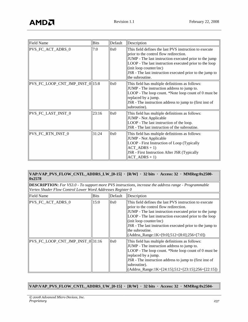
Revision 1.1 February 22, 2008
© 2008 Advanced Micro Devices, Inc. Proprietary 237
Field Name Bits Default Description
PVS_FC_ACT_ADRS_0 7:0 0x0 This field defines the last PVS instruction to execute
prior to the control flow redirection.
JUMP - The last instruction executed prior to the jump
LOOP - The last instruction executed prior to the loop
(init loop counter/inc)
JSR - The last instruction executed prior to the jump to
the subroutine.
PVS_FC_LOOP_CNT_JMP_INST_0 15:8 0x0 This field has multiple definitions as follows:
JUMP - The instruction address to jump to.
LOOP - The loop count. *Note loop count of 0 must be
replaced by a jump.
JSR - The instruction address to jump to (first inst of
subroutine).
PVS_FC_LAST_INST_0 23:16 0x0 This field has multiple definitions as follows:
JUMP - Not Applicable
LOOP - The last instruction of the loop.
JSR - The last instruction of the subroutine.
PVS_FC_RTN_INST_0 31:24 0x0 This field has multiple definitions as follows:
JUMP - Not Applicable
LOOP - First Instruction of Loop (Typically
ACT_ADRS + 1)
JSR - First Instruction After JSR (Typically
ACT_ADRS + 1)
VAP:VAP_PVS_FLOW_CNTL_ADDRS_LW_[0-15] · [R/W] · 32 bits · Access: 32 · MMReg:0x2500-
0x2578
DESCRIPTION: For VS3.0 - To support more PVS instructions, increase the address range - Programmable
Vertex Shader Flow Control Lower Word Addresses Register 0
Field Name Bits Default Description
PVS_FC_ACT_ADRS_0 15:0 0x0 This field defines the last PVS instruction to execute
prior to the control flow redirection.
JUMP - The last instruction executed prior to the jump
LOOP - The last instruction executed prior to the loop
(init loop counter/inc)
JSR - The last instruction executed prior to the jump to
the subroutine.
(Addrss_Range:1K=[9:0];512=[8:0];256=[7:0])
PVS_FC_LOOP_CNT_JMP_INST_0 31:16 0x0 This field has multiple definitions as follows:
JUMP - The instruction address to jump to.
LOOP - The loop count. *Note loop count of 0 must be
replaced by a jump.
JSR - The instruction address to jump to (first inst of
subroutine).
(Addrss_Range:1K=[24:15];512=[23:15];256=[22:15])
VAP:VAP_PVS_FLOW_CNTL_ADDRS_UW_[0-15] · [R/W] · 32 bits · Access: 32 · MMReg:0x2504-

Revision 1.1 February 22, 2008
© 2008 Advanced Micro Devices, Inc. Proprietary 238
0x257c
DESCRIPTION: For VS3.0 - To support more PVS instructions, increase the address range - Programmable
Vertex Shader Flow Control Upper Word Addresses Register 0
Field Name Bits Default Description
PVS_FC_LAST_INST_0 15:0 0x0 This field has multiple definitions as follows:
JUMP - Not Applicable
LOOP - The last instruction of the loop.
JSR - The last instruction of the subroutine.
(Addrss_Range:1K=[9:0];512=[8:0];256=[7:0])
PVS_FC_RTN_INST_0 31:16 0x0 This field has multiple definitions as follows:
JUMP - Not Applicable
LOOP - First Instruction of Loop (Typically
ACT_ADRS + 1)
JSR - First Instruction After JSR (Typically ACT_ADRS
+ 1).
(Addrss_Range:1K=[24:15];512=[23:15];256=[22:15])
VAP:VAP_PVS_FLOW_CNTL_LOOP_INDEX_[0-15] · [R/W] · 32 bits · Access: 32 · MMReg:0x2290-
0x22cc
DESCRIPTION: Programmable Vertex Shader Flow Control Loop Index Register 0
Field Name Bits Default Description
PVS_FC_LOOP_INIT_VAL_0 7:0 0x0 This field stores the automatic loop index register init
value. This is an 8-bit unsigned value 0-255. This field
is only used if the corresponding control flow
instruction is a loop.
PVS_FC_LOOP_STEP_VAL_0 15:8 0x0 This field stores the automatic loop index register step
value. This is an 8-bit 2`s comp signed value -128-127.
This field is only used if the corresponding control
flow instruction is a loop.
PVS_FC_LOOP_REPEAT_NO_FLI_0 31 0x0 When this field is set, the automatic loop index register
init value is not used at loop activation. The intial loop
index is inherited from outer loop. The loop index
register step value is used at the end of each loop
iteration ; after loop completion, the outer loop index
register is restored
VAP:VAP_PVS_FLOW_CNTL_OPC · [R/W] · 32 bits · Access: 32 · MMReg:0x22dc
DESCRIPTION: Programmable Vertex Shader Flow Control Opcode Register
Field Name Bits Default Description
PVS_FC_OPC_0 1:0 0x0 This opcode field determines what type of control flow
instruction to execute.
0 = NO_OP
1 = JUMP
2 = LOOP
3 = JSR (Jump to Subroutine)

Revision 1.1 February 22, 2008
© 2008 Advanced Micro Devices, Inc. Proprietary 239
PVS_FC_OPC_1 3:2 0x0 See PVS_FC_OPC_0.
PVS_FC_OPC_2 5:4 0x0 See PVS_FC_OPC_0.
PVS_FC_OPC_3 7:6 0x0 See PVS_FC_OPC_0.
PVS_FC_OPC_4 9:8 0x0 See PVS_FC_OPC_0.
PVS_FC_OPC_5 11:10 0x0 See PVS_FC_OPC_0.
PVS_FC_OPC_6 13:12 0x0 See PVS_FC_OPC_0.
PVS_FC_OPC_7 15:14 0x0 See PVS_FC_OPC_0.
PVS_FC_OPC_8 17:16 0x0 See PVS_FC_OPC_0.
PVS_FC_OPC_9 19:18 0x0 See PVS_FC_OPC_0.
PVS_FC_OPC_10 21:20 0x0 See PVS_FC_OPC_0.
PVS_FC_OPC_11 23:22 0x0 See PVS_FC_OPC_0.
PVS_FC_OPC_12 25:24 0x0 See PVS_FC_OPC_0.
PVS_FC_OPC_13 27:26 0x0 See PVS_FC_OPC_0.
PVS_FC_OPC_14 29:28 0x0 See PVS_FC_OPC_0.
PVS_FC_OPC_15 31:30 0x0 See PVS_FC_OPC_0.
VAP:VAP_PVS_STATE_FLUSH_REG · [R/W] · 32 bits · Access: 32 · MMReg:0x2284
Field Name Bits Default Description
DATA_REGISTER
(Access: W)
31:0 0x0 This register is used to force a flush of the PVS block
when single-buffered updates are performed. The multi-
state control of PVS Code and Const memories by the
driver is primarily for more flexible PVS state control
and for performance testing. When this register address
is written, the State Block will force a flush of PVS
processing so that both versions of PVS state are
available before updates are processed. This register is
write only, and the data that is written is unused.
VAP:VAP_PVS_VECTOR_DATA_REG · [R/W] · 32 bits · Access: 32 · MMReg:0x2204
Field Name Bits Default Description
DATA_REGISTER 31:0 0x0 32-bit data to write to Vector Memory. Used for PVS
code and Constant updates.
VAP:VAP_PVS_VECTOR_DATA_REG_128 · [W] · 32 bits · Access: 32 · MMReg:0x2208
Field Name Bits Default Description
DATA_REGISTER 31:0 0x0 128-bit data path to write to Vector Memory. Used for
PVS code and Constant updates.
VAP:VAP_PVS_VECTOR_INDX_REG · [R/W] · 32 bits · Access: 32 · MMReg:0x2200
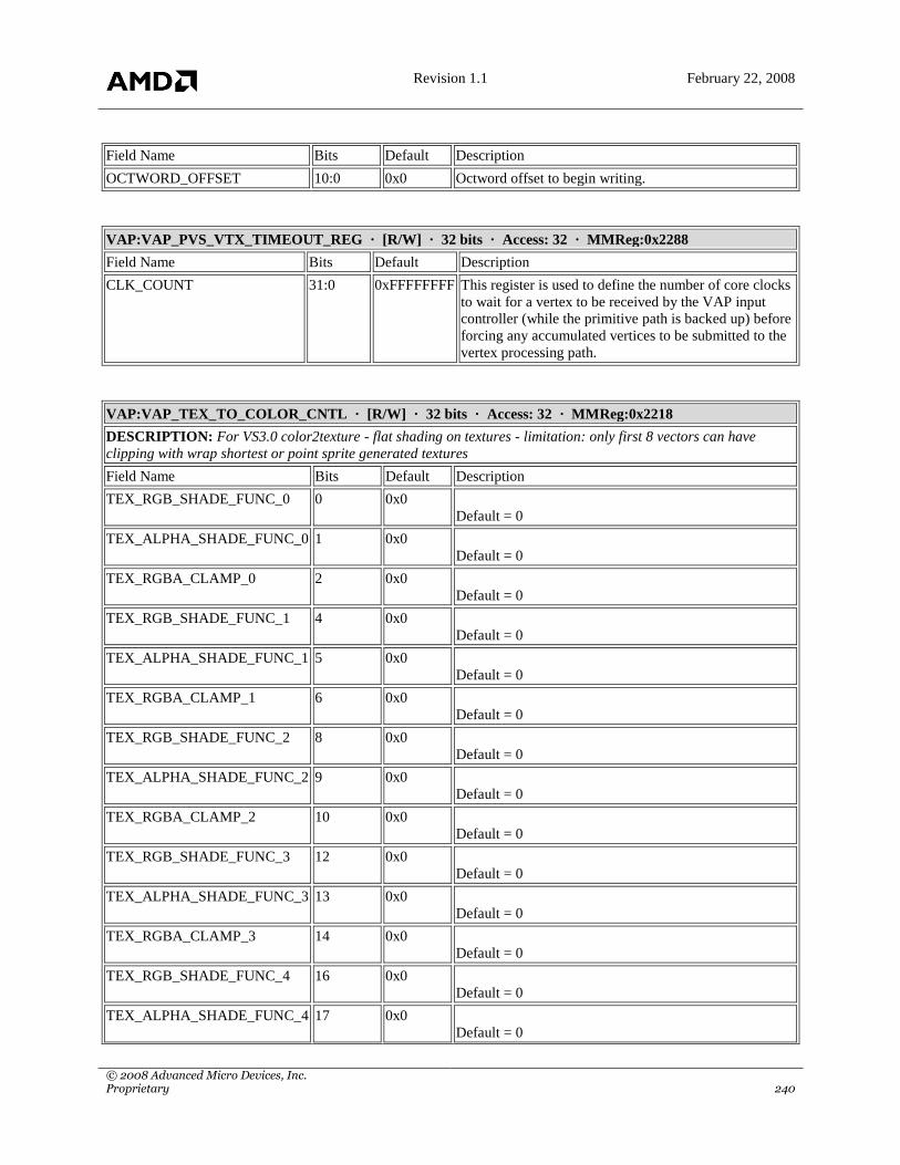
Revision 1.1 February 22, 2008
© 2008 Advanced Micro Devices, Inc. Proprietary 240
Field Name Bits Default Description
OCTWORD_OFFSET 10:0 0x0 Octword offset to begin writing.
VAP:VAP_PVS_VTX_TIMEOUT_REG · [R/W] · 32 bits · Access: 32 · MMReg:0x2288
Field Name Bits Default Description
CLK_COUNT 31:0 0xFFFFFFFF This register is used to define the number of core clocks
to wait for a vertex to be received by the VAP input
controller (while the primitive path is backed up) before
forcing any accumulated vertices to be submitted to the
vertex processing path.
VAP:VAP_TEX_TO_COLOR_CNTL · [R/W] · 32 bits · Access: 32 · MMReg:0x2218
DESCRIPTION: For VS3.0 color2texture - flat shading on textures - limitation: only first 8 vectors can have
clipping with wrap shortest or point sprite generated textures
Field Name Bits Default Description
TEX_RGB_SHADE_FUNC_0 0 0x0
Default = 0
TEX_ALPHA_SHADE_FUNC_0 1 0x0
Default = 0
TEX_RGBA_CLAMP_0 2 0x0
Default = 0
TEX_RGB_SHADE_FUNC_1 4 0x0
Default = 0
TEX_ALPHA_SHADE_FUNC_1 5 0x0
Default = 0
TEX_RGBA_CLAMP_1 6 0x0
Default = 0
TEX_RGB_SHADE_FUNC_2 8 0x0
Default = 0
TEX_ALPHA_SHADE_FUNC_2 9 0x0
Default = 0
TEX_RGBA_CLAMP_2 10 0x0
Default = 0
TEX_RGB_SHADE_FUNC_3 12 0x0
Default = 0
TEX_ALPHA_SHADE_FUNC_3 13 0x0
Default = 0
TEX_RGBA_CLAMP_3 14 0x0
Default = 0
TEX_RGB_SHADE_FUNC_4 16 0x0
Default = 0
TEX_ALPHA_SHADE_FUNC_4 17 0x0
Default = 0

Revision 1.1 February 22, 2008
© 2008 Advanced Micro Devices, Inc. Proprietary 241
TEX_RGBA_CLAMP_4 18 0x0
Default = 0
TEX_RGB_SHADE_FUNC_5 20 0x0
Default = 0
TEX_ALPHA_SHADE_FUNC_5 21 0x0
Default = 0
TEX_RGBA_CLAMP_5 22 0x0
Default = 0
TEX_RGB_SHADE_FUNC_6 24 0x0
Default = 0
TEX_ALPHA_SHADE_FUNC_6 25 0x0
Default = 0
TEX_RGBA_CLAMP_6 26 0x0
Default = 0
TEX_RGB_SHADE_FUNC_7 28 0x0
Default = 0
TEX_ALPHA_SHADE_FUNC_7 29 0x0
Default = 0
TEX_RGBA_CLAMP_7 30 0x0
Default = 0
VAP:VAP_VF_CNTL · [R/W] · 32 bits · Access: 32 · MMReg:0x2084
DESCRIPTION: Vertex Fetcher Control
Field Name Bits Default Description
PRIM_TYPE 3:0 0x0 Primitive Type
0 : None (will not trigger Setup Engine to run)
1 : Point List
2 : Line List
3 : Line Strip
4 : Triangle List
5 : Triangle Fan
6 : Triangle Strip
7 : Triangle with wFlags (aka, Rage128 `Type-2`
triangles) *
8-11 : Unused
12 : Line Loop
13 : Quad List
14 : Quad Strip
15 : Polygon
*Encoding 7 indicates whether a 16-bit word of wFlags
is present in the stream of indices arriving when the
VTX_AMODE is programmed as a `0`. The Setup
Engine just steps over the wFlags word; ignoring it.
0 = Stream contains just indices, as:
[ Index1, Index0]
[ Index3, Index2]
[ Index5, Index4 ]

Revision 1.1 February 22, 2008
© 2008 Advanced Micro Devices, Inc. Proprietary 242
etc...
1 = Stream contains indices and wFlags:
[ Index1, Index0]
[ wFlags,Index 2 ]
[ Index4, Index3]
[ wFlags, Index5 ]
etc...
PRIM_WALK 5:4 0x0 Method of Passing Vertex Data.
0 : State-Based Vertex Data. (Vertex data and tokens
embedded in command stream.)
1 = Indexes (Indices embedded in command stream;
vertex data to be fetched from memory.)
2 = Vertex List (Vertex data to be fetched from
memory.)
3 = Vertex Data (Vertex data embedded in command
stream.)
RSVD_PREV_USED 10:6 0x0 Reserved bits
INDEX_SIZE 11 0x0 When set, vertex indices are 32-bits/indx, otherwise, 16-
bits/indx.
VTX_REUSE_DIS 12 0x0 When set, vertex reuse is disabled. DO NOT SET unless
PRIM_WALK is Indexes.
DUAL_INDEX_MODE 13 0x0 When set, the incoming index is treated as two separate
indices. Bits 23-16 are used as the index for AOS 0
(These are 0 for 16-bit indices) Bits 15-0 are used as the
index for AOS 1-15. This mode was added specifically
for HOS usage
USE_ALT_NUM_VERTS 14 0x0 When set, the number of vertices in the command packet
is taken from VAP_ALT_NUM_VERTICES register
instead of bits 31:16 of VAP_VF_CNTL
NUM_VERTICES 31:16 0x0 Number of vertices in the command packet.
VAP:VAP_VF_MAX_VTX_INDX · [R/W] · 32 bits · Access: 32 · MMReg:0x2134
DESCRIPTION: Maximum Vertex Indx Clamp
Field Name Bits Default Description
MAX_INDX 23:0 0xFFFFFF If index to be fetched is larger than this value, the fetch
indx is set to MAX_INDX
VAP:VAP_VF_MIN_VTX_INDX · [R/W] · 32 bits · Access: 32 · MMReg:0x2138
DESCRIPTION: Minimum Vertex Indx Clamp
Field Name Bits Default Description
MIN_INDX 23:0 0x0 If index to be fetched is smaller than this value, the fetch
indx is set to MIN_INDX
VAP:VAP_VPORT_XOFFSET · [R/W] · 32 bits · Access: 32 · MMReg:0x1d9c, MMReg:0x209c

Revision 1.1 February 22, 2008
© 2008 Advanced Micro Devices, Inc. Proprietary 243
DESCRIPTION: Viewport Transform X Offset
Field Name Bits Default Description
VPORT_XOFFSET 31:0 0x0 Viewport Offset for X coordinates. An IEEE float.
VAP:VAP_VPORT_XSCALE · [R/W] · 32 bits · Access: 32 · MMReg:0x1d98, MMReg:0x2098
DESCRIPTION: Viewport Transform X Scale Factor
Field Name Bits Default Description
VPORT_XSCALE 31:0 0x0 Viewport Scale Factor for X coordinates. An IEEE float.
VAP:VAP_VPORT_YOFFSET · [R/W] · 32 bits · Access: 32 · MMReg:0x1da4, MMReg:0x20a4
DESCRIPTION: Viewport Transform Y Offset
Field Name Bits Default Description
VPORT_YOFFSET 31:0 0x0 Viewport Offset for Y coordinates. An IEEE float.
VAP:VAP_VPORT_YSCALE · [R/W] · 32 bits · Access: 32 · MMReg:0x1da0, MMReg:0x20a0
DESCRIPTION: Viewport Transform Y Scale Factor
Field Name Bits Default Description
VPORT_YSCALE 31:0 0x0 Viewport Scale Factor for Y coordinates. An IEEE float.
VAP:VAP_VPORT_ZOFFSET · [R/W] · 32 bits · Access: 32 · MMReg:0x1dac, MMReg:0x20ac
DESCRIPTION: Viewport Transform Z Offset
Field Name Bits Default Description
VPORT_ZOFFSET 31:0 0x0 Viewport Offset for Z coordinates. An IEEE float.
VAP:VAP_VPORT_ZSCALE · [R/W] · 32 bits · Access: 32 · MMReg:0x1da8, MMReg:0x20a8
DESCRIPTION: Viewport Transform Z Scale Factor
Field Name Bits Default Description
VPORT_ZSCALE 31:0 0x0 Viewport Scale Factor for Z coordinates. An IEEE float.
VAP:VAP_VTE_CNTL · [R/W] · 32 bits · Access: 32 · MMReg:0x20b0
DESCRIPTION: Viewport Transform Engine Control
Field Name Bits Default Description
VPORT_X_SCALE_ENA 0 0x0 Viewport Transform Scale Enable for X component
VPORT_X_OFFSET_ENA 1 0x0 Viewport Transform Offset Enable for X component
VPORT_Y_SCALE_ENA 2 0x0 Viewport Transform Scale Enable for Y component
VPORT_Y_OFFSET_ENA 3 0x0 Viewport Transform Offset Enable for Y component

Revision 1.1 February 22, 2008
© 2008 Advanced Micro Devices, Inc. Proprietary 244
VPORT_Z_SCALE_ENA 4 0x0 Viewport Transform Scale Enable for Z component
VPORT_Z_OFFSET_ENA 5 0x0 Viewport Transform Offset Enable for Z component
VTX_XY_FMT 8 0x0 Indicates that the incoming X, Y have already been
multiplied by 1/W0.
If OFF, the Setup Engine will bultiply the X, Y
coordinates by 1/W0.,
VTX_Z_FMT 9 0x0 Indicates that the incoming Z has already been multiplied
by 1/W0.
If OFF, the Setup Engine will multiply the Z coordinate
by 1/W0.
VTX_W0_FMT 10 0x0 Indicates that the incoming W0 is not 1/W0.
If ON, the Setup Engine will perform the reciprocal to
get 1/W0.
SERIAL_PROC_ENA 11 0x0 If set, x,y,z viewport transform are performed serially
through a single pipeline instead of in parallel. Used to
mimic RL300 design.
VAP:VAP_VTX_AOS_ADDR[0-15] · [R/W] · 32 bits · Access: 32 · MMReg:0x20c8-0x2120
DESCRIPTION: Array-of-Structures Address 0
Field Name Bits Default Description
VTX_AOS_ADDR0 31:2 0x0 Base Address of the Array of Structures.
VAP:VAP_VTX_AOS_ATTR[01-1415] · [R/W] · 32 bits · Access: 32 · MMReg:0x20c4-0x2118
DESCRIPTION: Array-of-Structures Attributes 0 & 1
Field Name Bits Default Description
VTX_AOS_COUNT0 6:0 0x0 Number of dwords in this structure.
VTX_AOS_STRIDE0 14:8 0x0 Number of dwords from one array element to the next.
VTX_AOS_COUNT1 22:16 0x0 Number of dwords in this structure.
VTX_AOS_STRIDE1 30:24 0x0 Number of dwords from one array element to the next.
VAP:VAP_VTX_NUM_ARRAYS · [R/W] · 32 bits · Access: 32 · MMReg:0x20c0
DESCRIPTION: Vertex Array of Structures Control
Field Name Bits Default Description
VTX_NUM_ARRAYS 4:0 0x0 The number of arrays required to represent the current
vertex type.
Each Array is described by the following three fields:
VTX_AOS_ADDR, VTX_AOS_COUNT,
VTX_AOS_STRIDE.
VC_FORCE_PREFETCH 5 0x0 Force Vertex Data Pre-fetching. If this bit is set, then a
256-bit word will always be fetched, regardless of which
dwords are needed. Typically useful when
VAP_VF_CNTL.PRIM_WALK is set to Vertex List

Revision 1.1 February 22, 2008
© 2008 Advanced Micro Devices, Inc. Proprietary 245
(Auto-incremented indices).
VC_DIS_CACHE_INVLD
(Access: R)
6 0x0 If set, the vertex cache is not invalidated between draw
packets. This allows vertex cache hits to occur from
packet to packet. This must be set with caution with
respect to multiple contexts in the driver.
AOS_0_FETCH_SIZE 16 0x0 Granule Size to Fetch for AOS 0.
0 = 128-bit granule size
1 = 256-bit granule size
This allows the driver to program the fetch size based on
DWORDS/VTX/AOS combined with AGP vs. LOC
Memory. The general belief is that the granule size
should always be 256-bits for LOC memory and AGP8X
data, but should be 128-bit for AGP2X/4X data if the
DWORDS/VTX/AOS is less than TBD (128?) bits.
AOS_1_FETCH_SIZE 17 0x0 See AOS_0_FETCH_SIZE
AOS_2_FETCH_SIZE 18 0x0 See AOS_0_FETCH_SIZE
AOS_3_FETCH_SIZE 19 0x0 See AOS_0_FETCH_SIZE
AOS_4_FETCH_SIZE 20 0x0 See AOS_0_FETCH_SIZE
AOS_5_FETCH_SIZE 21 0x0 See AOS_0_FETCH_SIZE
AOS_6_FETCH_SIZE 22 0x0 See AOS_0_FETCH_SIZE
AOS_7_FETCH_SIZE 23 0x0 See AOS_0_FETCH_SIZE
AOS_8_FETCH_SIZE 24 0x0 See AOS_0_FETCH_SIZE
AOS_9_FETCH_SIZE 25 0x0 See AOS_0_FETCH_SIZE
AOS_10_FETCH_SIZE 26 0x0 See AOS_0_FETCH_SIZE
AOS_11_FETCH_SIZE 27 0x0 See AOS_0_FETCH_SIZE
AOS_12_FETCH_SIZE 28 0x0 See AOS_0_FETCH_SIZE
AOS_13_FETCH_SIZE 29 0x0 See AOS_0_FETCH_SIZE
AOS_14_FETCH_SIZE 30 0x0 See AOS_0_FETCH_SIZE
AOS_15_FETCH_SIZE 31 0x0 See AOS_0_FETCH_SIZE
VAP:VAP_VTX_SIZE · [R/W] · 32 bits · Access: 32 · MMReg:0x20b4
DESCRIPTION: Vertex Size Specification Register
Field Name Bits Default Description
DWORDS_PER_VTX 6:0 0x0 This field specifies the number of DWORDS per vertex
to expect when VAP_VF_CNTL.PRIM_WALK is set to
Vertex Data (vertex data embedded in command stream).
This field is not used for any other PRIM_WALK
settings. This field replaces the usage of the
VAP_VTX_FMT_0/1 for this purpose in prior
implementations.
VAP:VAP_VTX_STATE_CNTL · [R/W] · 32 bits · Access: 32 · MMReg:0x2180
DESCRIPTION: VAP Vertex State Control Register

Revision 1.1 February 22, 2008
© 2008 Advanced Micro Devices, Inc. Proprietary 246
Field Name Bits Default Description
COLOR_0_ASSEMBLY_CNTL 1:0 0x0 0 : Select Color 0
1 : Select User Color 0
2 : Select User Color 1
3 : Reserved
COLOR_1_ASSEMBLY_CNTL 3:2 0x0 0 : Select Color 1
1 : Select User Color 0
2 : Select User Color 1
3 : Reserved
COLOR_2_ASSEMBLY_CNTL 5:4 0x0 0 : Select Color 2
1 : Select User Color 0
2 : Select User Color 1
3 : Reserved
COLOR_3_ASSEMBLY_CNTL 7:6 0x0 0 : Select Color 3
1 : Select User Color 0
2 : Select User Color 1
3 : Reserved
COLOR_4_ASSEMBLY_CNTL 9:8 0x0 0 : Select Color 4
1 : Select User Color 0
2 : Select User Color 1
3 : Reserved
COLOR_5_ASSEMBLY_CNTL 11:10 0x0 0 : Select Color 5
1 : Select User Color 0
2 : Select User Color 1
3 : Reserved
COLOR_6_ASSEMBLY_CNTL 13:12 0x0 0 : Select Color 6
1 : Select User Color 0
2 : Select User Color 1
3 : Reserved
COLOR_7_ASSEMBLY_CNTL 15:14 0x0 0 : Select Color 7
1 : Select User Color 0
2 : Select User Color 1
3 : Reserved
UPDATE_USER_COLOR_0_ENA 16 0x0 0 : User Color 0 State is NOT updated when User Color
0 is written.
1 : User Color 1 State IS updated when User Color 0 is
written.
Reserved 18 0x0 Set to 0
VAP:VAP_VTX_ST_BLND_WT_[0-3] · [R/W] · 32 bits · Access: 32 · MMReg:0x2430-0x243c
DESCRIPTION: Data register
Field Name Bits Default Description
DATA_REGISTER 31:0 0x0 BLND_WT_0
VAP:VAP_VTX_ST_CLR_[0-7]_A · [R/W] · 32 bits · Access: 32 · MMReg:0x232c-0x239c

Revision 1.1 February 22, 2008
© 2008 Advanced Micro Devices, Inc. Proprietary 247
DESCRIPTION: Data register
Field Name Bits Default Description
DATA_REGISTER 31:0 0x0 CLR_0_A
VAP:VAP_VTX_ST_CLR_[0-7]_B · [R/W] · 32 bits · Access: 32 · MMReg:0x2328-0x2398
DESCRIPTION: Data register
Field Name Bits Default Description
DATA_REGISTER 31:0 0x0 CLR_0_B
VAP:VAP_VTX_ST_CLR_[0-7]_G · [R/W] · 32 bits · Access: 32 · MMReg:0x2324-0x2394
DESCRIPTION: Data register
Field Name Bits Default Description
DATA_REGISTER 31:0 0x0 CLR_0_G
VAP:VAP_VTX_ST_CLR_[0-7]_PKD · [W] · 32 bits · Access: 32 · MMReg:0x2470-0x248c
DESCRIPTION: Data register
Field Name Bits Default Description
DATA_REGISTER 31:0 0x0 CLR_0_PKD
VAP:VAP_VTX_ST_CLR_[0-7]_R · [R/W] · 32 bits · Access: 32 · MMReg:0x2320-0x2390
DESCRIPTION: Data register
Field Name Bits Default Description
DATA_REGISTER 31:0 0x0 CLR_0_R
VAP:VAP_VTX_ST_DISC_FOG · [R/W] · 32 bits · Access: 32 · MMReg:0x2424
DESCRIPTION: Data register
Field Name Bits Default Description
DATA_REGISTER 31:0 0x0 DISC_FOG
VAP:VAP_VTX_ST_EDGE_FLAGS · [R/W] · 32 bits · Access: 32 · MMReg:0x245c
DESCRIPTION: Data register
Field Name Bits Default Description
DATA_REGISTER 0 0x0 EDGE_FLAGS
VAP:VAP_VTX_ST_END_OF_PKT · [W] · 32 bits · Access: 32 · MMReg:0x24ac

Revision 1.1 February 22, 2008
© 2008 Advanced Micro Devices, Inc. Proprietary 248
DESCRIPTION: Data register
Field Name Bits Default Description
DATA_REGISTER 31:0 0x0 END_OF_PKT
VAP:VAP_VTX_ST_NORM_0_PKD · [W] · 32 bits · Access: 32 · MMReg:0x2498
DESCRIPTION: Data register
Field Name Bits Default Description
DATA_REGISTER 31:0 0x0 NORM_0_PKD
VAP:VAP_VTX_ST_NORM_0_X · [R/W] · 32 bits · Access: 32 · MMReg:0x2310
DESCRIPTION: Data register
Field Name Bits Default Description
DATA_REGISTER 31:0 0x0 NORM_0_X
VAP:VAP_VTX_ST_NORM_0_Y · [R/W] · 32 bits · Access: 32 · MMReg:0x2314
DESCRIPTION: Data register
Field Name Bits Default Description
DATA_REGISTER 31:0 0x0 NORM_0_Y
VAP:VAP_VTX_ST_NORM_0_Z · [R/W] · 32 bits · Access: 32 · MMReg:0x2318
DESCRIPTION: Data register
Field Name Bits Default Description
DATA_REGISTER 31:0 0x0 NORM_0_Z
VAP:VAP_VTX_ST_NORM_1_X · [R/W] · 32 bits · Access: 32 · MMReg:0x2450
DESCRIPTION: Data register
Field Name Bits Default Description
DATA_REGISTER 31:0 0x0 NORM_1_X
VAP:VAP_VTX_ST_NORM_1_Y · [R/W] · 32 bits · Access: 32 · MMReg:0x2454
DESCRIPTION: Data register
Field Name Bits Default Description
DATA_REGISTER 31:0 0x0 NORM_1_Y
VAP:VAP_VTX_ST_NORM_1_Z · [R/W] · 32 bits · Access: 32 · MMReg:0x2458

Revision 1.1 February 22, 2008
© 2008 Advanced Micro Devices, Inc. Proprietary 249
DESCRIPTION: Data register
Field Name Bits Default Description
DATA_REGISTER 31:0 0x0 NORM_1_Z
VAP:VAP_VTX_ST_PNT_SPRT_SZ · [R/W] · 32 bits · Access: 32 · MMReg:0x2420
DESCRIPTION: Data register
Field Name Bits Default Description
DATA_REGISTER 31:0 0x0 PNT_SPRT_SZ
VAP:VAP_VTX_ST_POS_0_W_4 · [R/W] · 32 bits · Access: 32 · MMReg:0x230c
DESCRIPTION: Data register
Field Name Bits Default Description
DATA_REGISTER 31:0 0x0 POS_0_W
VAP:VAP_VTX_ST_POS_0_X_2 · [W] · 32 bits · Access: 32 · MMReg:0x2490
DESCRIPTION: Data register
Field Name Bits Default Description
DATA_REGISTER 31:0 0x0 POS_0_X_2
VAP:VAP_VTX_ST_POS_0_X_3 · [W] · 32 bits · Access: 32 · MMReg:0x24a0
DESCRIPTION: Data register
Field Name Bits Default Description
DATA_REGISTER 31:0 0x0 POS_0_X_3
VAP:VAP_VTX_ST_POS_0_X_4 · [R/W] · 32 bits · Access: 32 · MMReg:0x2300
DESCRIPTION: Data register
Field Name Bits Default Description
DATA_REGISTER 31:0 0x0 POS_0_X
VAP:VAP_VTX_ST_POS_0_Y_2 · [W] · 32 bits · Access: 32 · MMReg:0x2494
DESCRIPTION: Data register
Field Name Bits Default Description
DATA_REGISTER 31:0 0x0 POS_0_Y_2
VAP:VAP_VTX_ST_POS_0_Y_3 · [W] · 32 bits · Access: 32 · MMReg:0x24a4

Revision 1.1 February 22, 2008
© 2008 Advanced Micro Devices, Inc. Proprietary 250
DESCRIPTION: Data register
Field Name Bits Default Description
DATA_REGISTER 31:0 0x0 POS_0_Y_3
VAP:VAP_VTX_ST_POS_0_Y_4 · [R/W] · 32 bits · Access: 32 · MMReg:0x2304
DESCRIPTION: Data register
Field Name Bits Default Description
DATA_REGISTER 31:0 0x0 POS_0_Y
VAP:VAP_VTX_ST_POS_0_Z_3 · [W] · 32 bits · Access: 32 · MMReg:0x24a8
DESCRIPTION: Data register
Field Name Bits Default Description
DATA_REGISTER 31:0 0x0 POS_0_Z_3
VAP:VAP_VTX_ST_POS_0_Z_4 · [R/W] · 32 bits · Access: 32 · MMReg:0x2308
DESCRIPTION: Data register
Field Name Bits Default Description
DATA_REGISTER 31:0 0x0 POS_0_Z
VAP:VAP_VTX_ST_POS_1_W · [R/W] · 32 bits · Access: 32 · MMReg:0x244c
DESCRIPTION: Data register
Field Name Bits Default Description
DATA_REGISTER 31:0 0x0 POS_1_W
VAP:VAP_VTX_ST_POS_1_X · [R/W] · 32 bits · Access: 32 · MMReg:0x2440
DESCRIPTION: Data register
Field Name Bits Default Description
DATA_REGISTER 31:0 0x0 POS_1_X
VAP:VAP_VTX_ST_POS_1_Y · [R/W] · 32 bits · Access: 32 · MMReg:0x2444
DESCRIPTION: Data register
Field Name Bits Default Description
DATA_REGISTER 31:0 0x0 POS_1_Y
VAP:VAP_VTX_ST_POS_1_Z · [R/W] · 32 bits · Access: 32 · MMReg:0x2448
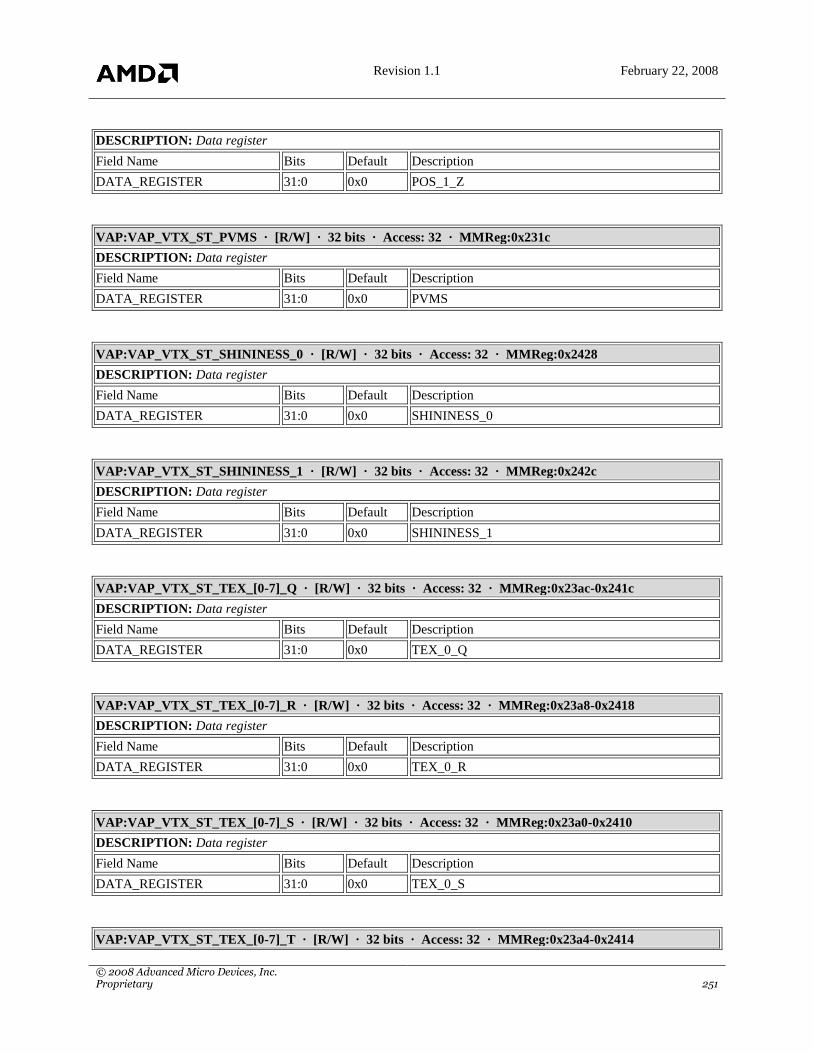
Revision 1.1 February 22, 2008
© 2008 Advanced Micro Devices, Inc. Proprietary 251
DESCRIPTION: Data register
Field Name Bits Default Description
DATA_REGISTER 31:0 0x0 POS_1_Z
VAP:VAP_VTX_ST_PVMS · [R/W] · 32 bits · Access: 32 · MMReg:0x231c
DESCRIPTION: Data register
Field Name Bits Default Description
DATA_REGISTER 31:0 0x0 PVMS
VAP:VAP_VTX_ST_SHININESS_0 · [R/W] · 32 bits · Access: 32 · MMReg:0x2428
DESCRIPTION: Data register
Field Name Bits Default Description
DATA_REGISTER 31:0 0x0 SHININESS_0
VAP:VAP_VTX_ST_SHININESS_1 · [R/W] · 32 bits · Access: 32 · MMReg:0x242c
DESCRIPTION: Data register
Field Name Bits Default Description
DATA_REGISTER 31:0 0x0 SHININESS_1
VAP:VAP_VTX_ST_TEX_[0-7]_Q · [R/W] · 32 bits · Access: 32 · MMReg:0x23ac-0x241c
DESCRIPTION: Data register
Field Name Bits Default Description
DATA_REGISTER 31:0 0x0 TEX_0_Q
VAP:VAP_VTX_ST_TEX_[0-7]_R · [R/W] · 32 bits · Access: 32 · MMReg:0x23a8-0x2418
DESCRIPTION: Data register
Field Name Bits Default Description
DATA_REGISTER 31:0 0x0 TEX_0_R
VAP:VAP_VTX_ST_TEX_[0-7]_S · [R/W] · 32 bits · Access: 32 · MMReg:0x23a0-0x2410
DESCRIPTION: Data register
Field Name Bits Default Description
DATA_REGISTER 31:0 0x0 TEX_0_S
VAP:VAP_VTX_ST_TEX_[0-7]_T · [R/W] · 32 bits · Access: 32 · MMReg:0x23a4-0x2414

Revision 1.1 February 22, 2008
© 2008 Advanced Micro Devices, Inc. Proprietary 252
DESCRIPTION: Data register
Field Name Bits Default Description
DATA_REGISTER 31:0 0x0 TEX_0_T
VAP:VAP_VTX_ST_USR_CLR_A · [R/W] · 32 bits · Access: 32 · MMReg:0x246c
DESCRIPTION: Data register
Field Name Bits Default Description
DATA_REGISTER 31:0 0x0 USR_CLR_A
VAP:VAP_VTX_ST_USR_CLR_B · [R/W] · 32 bits · Access: 32 · MMReg:0x2468
DESCRIPTION: Data register
Field Name Bits Default Description
DATA_REGISTER 31:0 0x0 USR_CLR_B
VAP:VAP_VTX_ST_USR_CLR_G · [R/W] · 32 bits · Access: 32 · MMReg:0x2464
DESCRIPTION: Data register
Field Name Bits Default Description
DATA_REGISTER 31:0 0x0 USR_CLR_G
VAP:VAP_VTX_ST_USR_CLR_PKD · [W] · 32 bits · Access: 32 · MMReg:0x249c
DESCRIPTION: Data register
Field Name Bits Default Description
DATA_REGISTER 31:0 0x0 USR_CLR_PKD
VAP:VAP_VTX_ST_USR_CLR_R · [R/W] · 32 bits · Access: 32 · MMReg:0x2460
DESCRIPTION: Data register
Field Name Bits Default Description
DATA_REGISTER 31:0 0x0 USR_CLR_R

Revision 1.1 February 22, 2008
© 2008 Advanced Micro Devices, Inc. Proprietary 253
10.11 Z Buffer Registers
ZB:ZB_BW_CNTL · [R/W] · 32 bits · Access: 8/16/32 · MMReg:0x4f1c
DESCRIPTION: Z Buffer Band-Width Control
Field Name Bits Defa
ult Description
HIZ_ENABLE 0 0x0 Enables hierarchical Z.
POSSIBLE VALUES:
00 - Hierarchical Z Disabled
01 - Hierarchical Z Enabled
HIZ_MIN 1 0x0 POSSIBLE VALUES:
00 - Update Hierarchical Z with Max value
01 - Update Hierarchical Z with Min value
FAST_FILL 2 0x0 POSSIBLE VALUES:
00 - Fast Fill Disabled
01 - Fast Fill Enabled (ZB_DEPTHCLEARVALUE )
RD_COMP_ENABLE 3 0x0 Enables reading of compressed Z data from memory to the
cache.
POSSIBLE VALUES:
00 - Z Read Compression Disabled
01 - Z Read Compression Enabled
WR_COMP_ENABLE 4 0x0 Enables writing of compressed Z data from cache to memory,
POSSIBLE VALUES:
00 - Z Write Compression Disabled
01 - Z Write Compression Enabled
ZB_CB_CLEAR 5 0x0 This bit is set when the Z buffer is used to help the CB in
clearing a region. Part of the region is cleared by the color
buffer and part will be cleared by the Z buffer. Since the Z
buffer does not have any write masks in the cache, full micro-
tiles need to be written. If a partial micro-tile is touched, then
the un-touched part will be unknowns. The cache will operate
in write-allocate mode and quads will be accumulated in the
cache and then evicted to main memory. The color value is
supplied through the ZB_DEPTHCLEARVALUE register.
POSSIBLE VALUES:
00 - Z unit cache controller does RMW
01 - Z unit cache controller does cache-line granular Write
only
FORCE_COMPRESSED_STENCIL_V
ALUE
6 0x0 Enabling this bit will force all the compressed stencil values
to be equal to
old_stencil_value&~ZB_STENCILREFMASK.stencilwritem
ask |
ZB_STENCILREFMASK.stencilref&ZB_STENCILREFMA
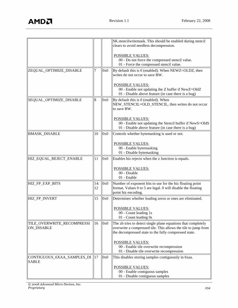
Revision 1.1 February 22, 2008
© 2008 Advanced Micro Devices, Inc. Proprietary 254
SK.stencilwritemask. This should be enabled during stencil
clears to avoid needless decompression.
POSSIBLE VALUES:
00 - Do not force the compressed stencil value.
01 - Force the compressed stencil value.
ZEQUAL_OPTIMIZE_DISABLE 7 0x0 By default this is 0 (enabled). When NEWZ=OLDZ, then
writes do not occur to save BW.
POSSIBLE VALUES:
00 - Enable not updating the Z buffer if NewZ=OldZ
01 - Disable above feature (in case there is a bug)
SEQUAL_OPTIMIZE_DISABLE 8 0x0 By default this is 0 (enabled). When
NEW_STENCIL=OLD_STENCIL, then writes do not occur
to save BW.
POSSIBLE VALUES:
00 - Enable not updating the Stencil buffer if NewS=OldS
01 - Disable above feature (in case there is a bug)
BMASK_DISABLE 10 0x0 Controls whether bytemasking is used or not.
POSSIBLE VALUES:
00 - Enable bytemasking
01 - Disable bytemasking
HIZ_EQUAL_REJECT_ENABLE 11 0x0 Enables hiz rejects when the z function is equals.
POSSIBLE VALUES:
00 - Disable
01 - Enable
HIZ_FP_EXP_BITS 14:
12
0x0 Number of exponent bits to use for the hiz floating point
format. Values 0 to 5 are legal. 0 will disable the floating
point hiz encoding.
HIZ_FP_INVERT 15 0x0 Determines whether leading zeros or ones are eliminated.
POSSIBLE VALUES:
00 - Count leading 1s
01 - Count leading 0s
TILE_OVERWRITE_RECOMPRESSI
ON_DISABLE
16 0x0 The zb tries to detect single plane equations that completely
overwrite a compressed tile. This allows the tile to jump from
the decompressed state to the fully compressed state.
POSSIBLE VALUES:
00 - Enable tile overwrite recompression
01 - Disable tile overwrite recompression
CONTIGUOUS_6XAA_SAMPLES_DI
SABLE
17 0x0 This disables storing samples contiguously in 6xaa.
POSSIBLE VALUES:
00 - Enable contiguous samples
01 - Disable contiguous samples

Revision 1.1 February 22, 2008
© 2008 Advanced Micro Devices, Inc. Proprietary 255
PEQ_PACKING_ENABLE 18 0x0 Enables packing of the plane equations to eliminate wasted
peq slots.
POSSIBLE VALUES:
00 - Disable
01 - Enable
COVERED_PTR_MASKING_ENABL
E
19 0x0 Enables discarding of pointers from pixels that are going to be
covered. This reduces the apparent number of plane equations
in use.
POSSIBLE VALUES:
00 - Disable
01 - Enable
ZB:ZB_CNTL · [R/W] · 32 bits · Access: 8/16/32 · MMReg:0x4f00
DESCRIPTION: Z Buffer Control
Field Name Bits Default Description
STENCIL_ENABLE 0 0x0 Enables stenciling.
POSSIBLE VALUES:
00 - Disabled
01 - Enabled
Z_ENABLE 1 0x0 Enables Z functions.
POSSIBLE VALUES:
00 - Disabled
01 - Enabled
ZWRITEENABLE 2 0x0 Enables writing of the Z buffer.
POSSIBLE VALUES:
00 - Disable
01 - Enable
ZSIGNED_COMPARE 3 0x0 Enable signed Z buffer comparison , for W-buffering.
POSSIBLE VALUES:
00 - Disable
01 - Enable
STENCIL_FRONT_BACK 4 0x0 When STENCIL_ENABLE is set, setting
STENCIL_FRONT_BACK bit to one specifies that
stencilfunc/stencilfail/stencilzpass/stencilzfail registers are
used if the quad is generated from front faced primitive
and
stencilfunc_bf/stencilfail_bf/stencilzpass_bf/stencilzfail_bf
are used if the quad is generated from a back faced
primitive. If the STENCIL_FRONT_BACK is not set,
then stencilfunc/stencilfail/stencilzpass/stencilzfail
registers determine the operation independent of the
front/back face state of the quad.

Revision 1.1 February 22, 2008
© 2008 Advanced Micro Devices, Inc. Proprietary 256
POSSIBLE VALUES:
00 - Disable
01 - Enable
ZSIGNED_MAGNITUDE 5 0x0 Specifies the signed number type to use for the Z buffer
comparison. This only has an effect when
ZSIGNED_COMPARE is enabled.
POSSIBLE VALUES:
00 - Twos complement
01 - Signed magnitude
STENCIL_REFMASK_FRONT_BACK 6 0x0 POSSIBLE VALUES:
00 - Disable
01 - Enable
ZB:ZB_DEPTHCLEARVALUE · [R/W] · 32 bits · Access: 8/16/32 · MMReg:0x4f28
DESCRIPTION: Z Buffer Clear Value
Field Name Bits Default Description
DEPTHCLEARVALUE 31:0 0x0 When a block has a Z Mask value of 0, all Z values in
that block are cleared to this value. In 24bpp, the stencil
value is also updated regardless of whether it is enabled
or not.
ZB:ZB_DEPTHOFFSET · [R/W] · 32 bits · Access: 8/16/32 · MMReg:0x4f20
DESCRIPTION: Z Buffer Address Offset
Field Name Bits Default Description
DEPTHOFFSET 31:5 0x0 2K aligned Z buffer address offset for macro tiles.
ZB:ZB_DEPTHPITCH · [R/W] · 32 bits · Access: 8/16/32 · MMReg:0x4f24
DESCRIPTION: Z Buffer Pitch and Endian Control
Field Name Bits Default Description
DEPTHPITCH 13:2 0x0 Z buffer pitch in multiples of 4 pixels.
DEPTHMACROTILE 16 0x0 Specifies whether Z buffer is macro-tiled. macro-tiles are
2K aligned
POSSIBLE VALUES:
00 - macro tiling disabled
01 - macro tiling enabled
DEPTHMICROTILE 18:17 0x0 Specifies whether Z buffer is micro-tiled. micro-tiles is
32 bytes
POSSIBLE VALUES:
00 - 32 byte cache line is linear
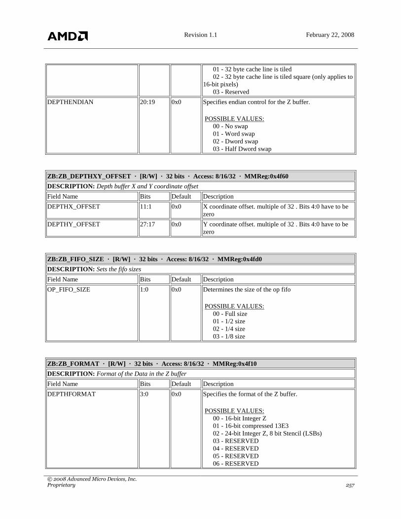
Revision 1.1 February 22, 2008
© 2008 Advanced Micro Devices, Inc. Proprietary 257
01 - 32 byte cache line is tiled
02 - 32 byte cache line is tiled square (only applies to
16-bit pixels)
03 - Reserved
DEPTHENDIAN 20:19 0x0 Specifies endian control for the Z buffer.
POSSIBLE VALUES:
00 - No swap
01 - Word swap
02 - Dword swap
03 - Half Dword swap
ZB:ZB_DEPTHXY_OFFSET · [R/W] · 32 bits · Access: 8/16/32 · MMReg:0x4f60
DESCRIPTION: Depth buffer X and Y coordinate offset
Field Name Bits Default Description
DEPTHX_OFFSET 11:1 0x0 X coordinate offset. multiple of 32 . Bits 4:0 have to be
zero
DEPTHY_OFFSET 27:17 0x0 Y coordinate offset. multiple of 32 . Bits 4:0 have to be
zero
ZB:ZB_FIFO_SIZE · [R/W] · 32 bits · Access: 8/16/32 · MMReg:0x4fd0
DESCRIPTION: Sets the fifo sizes
Field Name Bits Default Description
OP_FIFO_SIZE 1:0 0x0 Determines the size of the op fifo
POSSIBLE VALUES:
00 - Full size
01 - 1/2 size
02 - 1/4 size
03 - 1/8 size
ZB:ZB_FORMAT · [R/W] · 32 bits · Access: 8/16/32 · MMReg:0x4f10
DESCRIPTION: Format of the Data in the Z buffer
Field Name Bits Default Description
DEPTHFORMAT 3:0 0x0 Specifies the format of the Z buffer.
POSSIBLE VALUES:
00 - 16-bit Integer Z
01 - 16-bit compressed 13E3
02 - 24-bit Integer Z, 8 bit Stencil (LSBs)
03 - RESERVED
04 - RESERVED
05 - RESERVED
06 - RESERVED
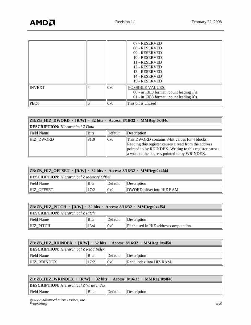
Revision 1.1 February 22, 2008
© 2008 Advanced Micro Devices, Inc. Proprietary 258
07 - RESERVED
08 - RESERVED
09 - RESERVED
10 - RESERVED
11 - RESERVED
12 - RESERVED
13 - RESERVED
14 - RESERVED
15 - RESERVED
INVERT 4 0x0 POSSIBLE VALUES:
00 - in 13E3 format , count leading 1`s
01 - in 13E3 format , count leading 0`s.
PEQ8 5 0x0 This bit is unused
ZB:ZB_HIZ_DWORD · [R/W] · 32 bits · Access: 8/16/32 · MMReg:0x4f4c
DESCRIPTION: Hierarchical Z Data
Field Name Bits Default Description
HIZ_DWORD 31:0 0x0 This DWORD contains 8-bit values for 4 blocks..
Reading this register causes a read from the address
pointed to by RDINDEX. Writing to this register causes
a write to the address pointed to by WRINDEX.
ZB:ZB_HIZ_OFFSET · [R/W] · 32 bits · Access: 8/16/32 · MMReg:0x4f44
DESCRIPTION: Hierarchical Z Memory Offset
Field Name Bits Default Description
HIZ_OFFSET 17:2 0x0 DWORD offset into HiZ RAM.
ZB:ZB_HIZ_PITCH · [R/W] · 32 bits · Access: 8/16/32 · MMReg:0x4f54
DESCRIPTION: Hierarchical Z Pitch
Field Name Bits Default Description
HIZ_PITCH 13:4 0x0 Pitch used in HiZ address computation.
ZB:ZB_HIZ_RDINDEX · [R/W] · 32 bits · Access: 8/16/32 · MMReg:0x4f50
DESCRIPTION: Hierarchical Z Read Index
Field Name Bits Default Description
HIZ_RDINDEX 17:2 0x0 Read index into HiZ RAM.
ZB:ZB_HIZ_WRINDEX · [R/W] · 32 bits · Access: 8/16/32 · MMReg:0x4f48
DESCRIPTION: Hierarchical Z Write Index
Field Name Bits Default Description
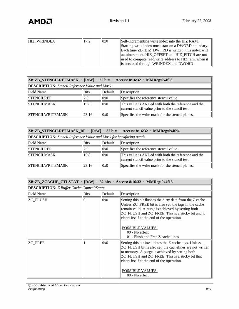
Revision 1.1 February 22, 2008
© 2008 Advanced Micro Devices, Inc. Proprietary 259
HIZ_WRINDEX 17:2 0x0 Self-incrementing write index into the HiZ RAM.
Starting write index must start on a DWORD boundary.
Each time ZB_HIZ_DWORD is written, this index will
autoincrement. HIZ_OFFSET and HIZ_PITCH are not
used to compute read/write address to HIZ ram, when it
is accessed through WRINDEX and DWORD
ZB:ZB_STENCILREFMASK · [R/W] · 32 bits · Access: 8/16/32 · MMReg:0x4f08
DESCRIPTION: Stencil Reference Value and Mask
Field Name Bits Default Description
STENCILREF 7:0 0x0 Specifies the reference stencil value.
STENCILMASK 15:8 0x0 This value is ANDed with both the reference and the
current stencil value prior to the stencil test.
STENCILWRITEMASK 23:16 0x0 Specifies the write mask for the stencil planes.
ZB:ZB_STENCILREFMASK_BF · [R/W] · 32 bits · Access: 8/16/32 · MMReg:0x4fd4
DESCRIPTION: Stencil Reference Value and Mask for backfacing quads
Field Name Bits Default Description
STENCILREF 7:0 0x0 Specifies the reference stencil value.
STENCILMASK 15:8 0x0 This value is ANDed with both the reference and the
current stencil value prior to the stencil test.
STENCILWRITEMASK 23:16 0x0 Specifies the write mask for the stencil planes.
ZB:ZB_ZCACHE_CTLSTAT · [R/W] · 32 bits · Access: 8/16/32 · MMReg:0x4f18
DESCRIPTION: Z Buffer Cache Control/Status
Field Name Bits Default Description
ZC_FLUSH 0 0x0 Setting this bit flushes the dirty data from the Z cache.
Unless ZC_FREE bit is also set, the tags in the cache
remain valid. A purge is achieved by setting both
ZC_FLUSH and ZC_FREE. This is a sticky bit and it
clears itself at the end of the operation.
POSSIBLE VALUES:
00 - No effect
01 - Flush and Free Z cache lines
ZC_FREE 1 0x0 Setting this bit invalidates the Z cache tags. Unless
ZC_FLUSH bit is also set, the cachelines are not written
to memory. A purge is achieved by setting both
ZC_FLUSH and ZC_FREE. This is a sticky bit that
clears itself at the end of the operation.
POSSIBLE VALUES:
00 - No effect

Revision 1.1 February 22, 2008
© 2008 Advanced Micro Devices, Inc. Proprietary 260
01 - Free Z cache lines (invalidate)
ZC_BUSY 31 0x0 This bit is unused ...
POSSIBLE VALUES:
00 - Idle
01 - Busy
ZB:ZB_ZPASS_ADDR · [R/W] · 32 bits · Access: 8/16/32 · MMReg:0x4f5c
DESCRIPTION: Z Buffer Z Pass Counter Address
Field Name Bits Default Description
ZPASS_ADDR 31:2 0x0 Writing this location with a DWORD address causes the
value in ZB_ZPASS_DATA to be written to main
memory at the location pointed to by this address.
NOTE: R300 has 2 pixel pipes. Broadcasting this address
causes both pipes to write their ZPASS value to the same
address. There is no guarantee which pipe will write last.
So when writing to this register, the GA needs to be
programmed to send the write command to pipe 0. Then
a different address needs to be written to pipe 1. Then
both pipes should be enabled for further register writes.
ZB:ZB_ZPASS_DATA · [R/W] · 32 bits · Access: 8/16/32 · MMReg:0x4f58
DESCRIPTION: Z Buffer Z Pass Counter Data
Field Name Bits Default Description
ZPASS_DATA 31:0 0x0 Contains the number of Z passed pixels since the last
write to this location. Writing this location resets the
count to the value written.
ZB:ZB_ZSTENCILCNTL · [R/W] · 32 bits · Access: 8/16/32 · MMReg:0x4f04
DESCRIPTION: Z and Stencil Function Control
Field Name Bits Default Description
ZFUNC 2:0 0x0 Specifies the Z function.
POSSIBLE VALUES:
00 - Never
01 - Less
02 - Less or Equal
03 - Equal
04 - Greater or Equal
05 - Greater Than
06 - Not Equal
07 - Always
STENCILFUNC 5:3 0x0 Specifies the stencil function.
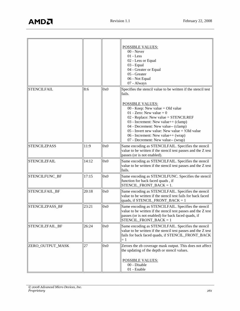
Revision 1.1 February 22, 2008
© 2008 Advanced Micro Devices, Inc. Proprietary 261
POSSIBLE VALUES:
00 - Never
01 - Less
02 - Less or Equal
03 - Equal
04 - Greater or Equal
05 - Greater
06 - Not Equal
07 - Always
STENCILFAIL 8:6 0x0 Specifies the stencil value to be written if the stencil test
fails.
POSSIBLE VALUES:
00 - Keep: New value = Old value
01 - Zero: New value = 0
02 - Replace: New value = STENCILREF
03 - Increment: New value++ (clamp)
04 - Decrement: New value-- (clamp)
05 - Invert new value: New value = !Old value
06 - Increment: New value++ (wrap)
07 - Decrement: New value-- (wrap)
STENCILZPASS 11:9 0x0 Same encoding as STENCILFAIL. Specifies the stencil
value to be written if the stencil test passes and the Z test
passes (or is not enabled).
STENCILZFAIL 14:12 0x0 Same encoding as STENCILFAIL. Specifies the stencil
value to be written if the stencil test passes and the Z test
fails.
STENCILFUNC_BF 17:15 0x0 Same encoding as STENCILFUNC. Specifies the stencil
function for back faced quads , if
STENCIL_FRONT_BACK = 1.
STENCILFAIL_BF 20:18 0x0 Same encoding as STENCILFAIL. Specifies the stencil
value to be written if the stencil test fails for back faced
quads, if STENCIL_FRONT_BACK = 1
STENCILZPASS_BF 23:21 0x0 Same encoding as STENCILFAIL. Specifies the stencil
value to be written if the stencil test passes and the Z test
passes (or is not enabled) for back faced quads, if
STENCIL_FRONT_BACK = 1
STENCILZFAIL_BF 26:24 0x0 Same encoding as STENCILFAIL. Specifies the stencil
value to be written if the stencil test passes and the Z test
fails for back faced quads, if STENCIL_FRONT_BACK
= 1
ZERO_OUTPUT_MASK 27 0x0 Zeroes the zb coverage mask output. This does not affect
the updating of the depth or stencil values.
POSSIBLE VALUES:
00 - Disable
01 - Enable

Revision 1.1 February 22, 2008
© 2008 Advanced Micro Devices, Inc. Proprietary 262
ZB:ZB_ZTOP · [R/W] · 32 bits · Access: 8/16/32 · MMReg:0x4f14
Field Name Bits Default Description
ZTOP 0 0x0 POSSIBLE VALUES:
00 - Z is at the bottom of the pipe, after the fog unit.
01 - Z is at the top of the pipe, after the scan unit.