RADC-TR-77-261 Teehnical Report TRW Defense and Space … · tN UNCLASSIFIED SECURITY...
58
RADC-TR-77-261 S Final Teehnical Report August 1977 TRW Defense and Space Systema Approved for public release; distribution unliated. Ii C:> ROME AIR DEVELOPMENT CENTER C-.. Air Force Systems Command -3 Gfiffiss Air Force Base, New York 13441 ~LL- iso C=- < .. I 5 z -
Transcript of RADC-TR-77-261 Teehnical Report TRW Defense and Space … · tN UNCLASSIFIED SECURITY...

RADC-TR-77-261
S Final Teehnical ReportAugust 1977
TRW Defense and Space Systema
Approved for public release; distribution unliated.
IiC:> ROME AIR DEVELOPMENT CENTER
C-.. Air Force Systems Command-3 Gfiffiss Air Force Base, New York 13441
~LL-
iso C=- < .. I
5 z -

This report has been reviewed by the RADC Information Office (01)and is releasable to the National Technical Information Service (NTIS).At NTIS it will be releasable to the general public, including foreignnations.
This report has been reviewed and approved for publication.
APPROVED:
LEWIS A. JAVARONEProject Engineer
APPROVED:
FRED I. DIAMONDTechnical DirectorCommunications and Control Division
FOR THE COHMA!NDER: 4 t%6?> 2JOHN P. RUSS
Acting Chief, Plans Office
If your address ha hanged or if you wish to be removed from the RADCmailing list, or if the addressee is no longer employed by your organization,please notify RADC (DAP) Griffiss AFB NY 13441. This will assist us inmaintaining a current mailing list.
Do not return this copy. Retain or destroy.

a UNCLASSIFIED
* S~~~~~~~~ECURITXX ,SSIFICATION OF THIS PAGE (When D~ettgntered),_________________
READ INSTRUCTIONS
*4. TITLE (and Subtitle) 1INE0pRP T
DonadL. chhed /5 F3i6.02-76c-,8c'
'4DBN IIA RASITRRCIE, a 06 rf 7
-------- NEDULE
I7 OIT RITO STTEE. (o th. -UMBERt)
9S. SPLEROMENT RARYNIZTOTES EADADES 0 RGA LMETRJC.TS
LRefeise A. Savare SDystem.
500~~910 Ip iitlLn0.ffs A FBTAC (CNtiu 1344 13.re NUMBE Of PAGES n Ietfyb bokum
evlatd E4K cohren QPESK an different iao Cnrllyn S coECRenTY CLASS. (fthireporet)ca
DO ~147 ED~iO OF1 NO SSIS USOETEUNCLASSIFIED
SECURITY SA ECLASSIFICATONOFTHIS DAO WeNGRDIt NteeG
Samel
14.SPLMETR OE
RAD Prjc Engineer:

I UNCLASSIFIEDSECURITY CLASSIFICATION OF THIS PAGE(lWlh. Data Er-e,.d
I
tN
UNCLASSIFIEDSECURITY CLASSIFICATIONI OF PAGE(Vhefl Date Entered)
Lk~
-- ----.-- -- .,4

TABLE OF CONTENTS
SECTION PAGE
I. INTRODUCTION AND SUMMARY 1
II. PROGRAM TEST RESULTS 2
2.1 Link Characterization 3
2.2 Digital Terminal Characterization 6
2.2.1 Digital Terminal Tests/MSK Modulation 6
2.2.2 Digital Terminal Tests/Coherent QPSK Modulation 8
2.2.3 Digital Terminal Tests/Differentially Coherent QPSw(Modulation 11
2.3 COMBINED DIGITAL TERMINAL/Ka-BAND LINK TESTS 16
2.3.1 Demonstration Link Tests/MSK Modulation 16
2.3.2 Demonstration Link Tests/Coherent QPSK Modulation 20
2.3.3 Demonstration Link Tests/Differentially Coherent QPSKModulation 22
III. HARDWARE DESCRIPTION 28
3.1 Ka-BAND DEMONSTRATION LINK DESCRIPTION 28
3.1.1 S-Band Frequency Sources 29
3.1.2 X9 Multiplier 29
3.1.3 Doubler/Upconverter 31
3.1.4 Avalanche Diode Amplifier 32
3.1.5 Ka-Band Downconverter 32
3.2 Digital Terminal Description 33
3.2.1 Multiplexer 33
3.2.2 Differential Encoder 34
3.2.3 QPSK Modulator 35
3.2.4 MSK Modulator Description 36
3.2.5 IF Noise Source 38
3.2.6 Quadriphase Demodulator 38
3.2.7 Differential Demodulator 39
3.2.8 Bit Sychronizer 393.2.9 Demultiplexer 41
APPENDIX. WIDEBAND DIGITAL TRANSMITTER/RECEIVER TEST PLAN 42
iii

LIST OF ILLUSTRATIONS
FIGURE PAGE
I Ka-Band Upconverter/D[wnconverter Gain Variation 4
2 Ka-Band Upconverter/Downconverter Phase Nonlinearity 4
3 Ka-Band ADA Gain Variation 4
4 Ka-Band ADA Phase Nonlinearity 5
5 Bandpass Filter Insertion Loss 5
6 Bandpass Filter Phase Nonlinearity 5
7 Ka-Band Demonstration Link Total Passband Response 6
8 MSK Digital Terminal Test Configuration 6
9 MSK Digital Terminal BER Performance 7
10 MSK Modulator Output Spectrum 8
11 Dinital Terminal Waveforms 9
12 Coherent QPSK Digital Terminal Test Configuration13 Coherent QPSK Digital Terminal BER Perform 10
14 Coherent QPSK Modulator Output Spectrum 11
15 Digital Terminal Demodulated Waveforms 12
16 Differentially Coherent QPSK Digital Terminal Test Configuration 13
17 Differentially Coherent QPSK Digital Terminal BER Performance 13
18 Differentially Coherent QPSK Modulator Output Spectrum 14
19 Digital Terminal Demodulated Waveforms 15
20 MSK Demonstration Link Test Configuration 16
21 Ka-Band Demonstration Link MSK BER Performance 17
22 MSK Modulated Signal Spectrum at Output of Ka-Band DemonstrationLink 18
23 Signals After Transmission Through the Ka-Band Demonstration Link 19
24 Coheruit QPSK Demonstration Link Test Configuration 20
25 Ka-Band Demonstration Link Coherent QPSK BER Performance 21
26 Coherent QPSK Modulator Spectrum After Transmission Through theKa-Band Demonstration Link 22
27 Signals After Transmission Through the Ka-Band Demonstration Link 23
28 Differential Coherent QPSK Demonstration Link Test Configuration 24
29 Ka-Band Demonstration Link Differentially Coherent QPSK BERPerformance 24
30 Differentially Coherent QPSK Modulated Spectrum After TransmissionThrough the Ka-Band Demonstration Link 25
31 Differentially Coherent QPSK After Transmission Through theDemonstration Link 27
32 Ka-Band Demonstration Link 28
33. S-Band Frequency Source 29
34 X9 Multiplier/Avalanche Diode Oscillator 30
iv
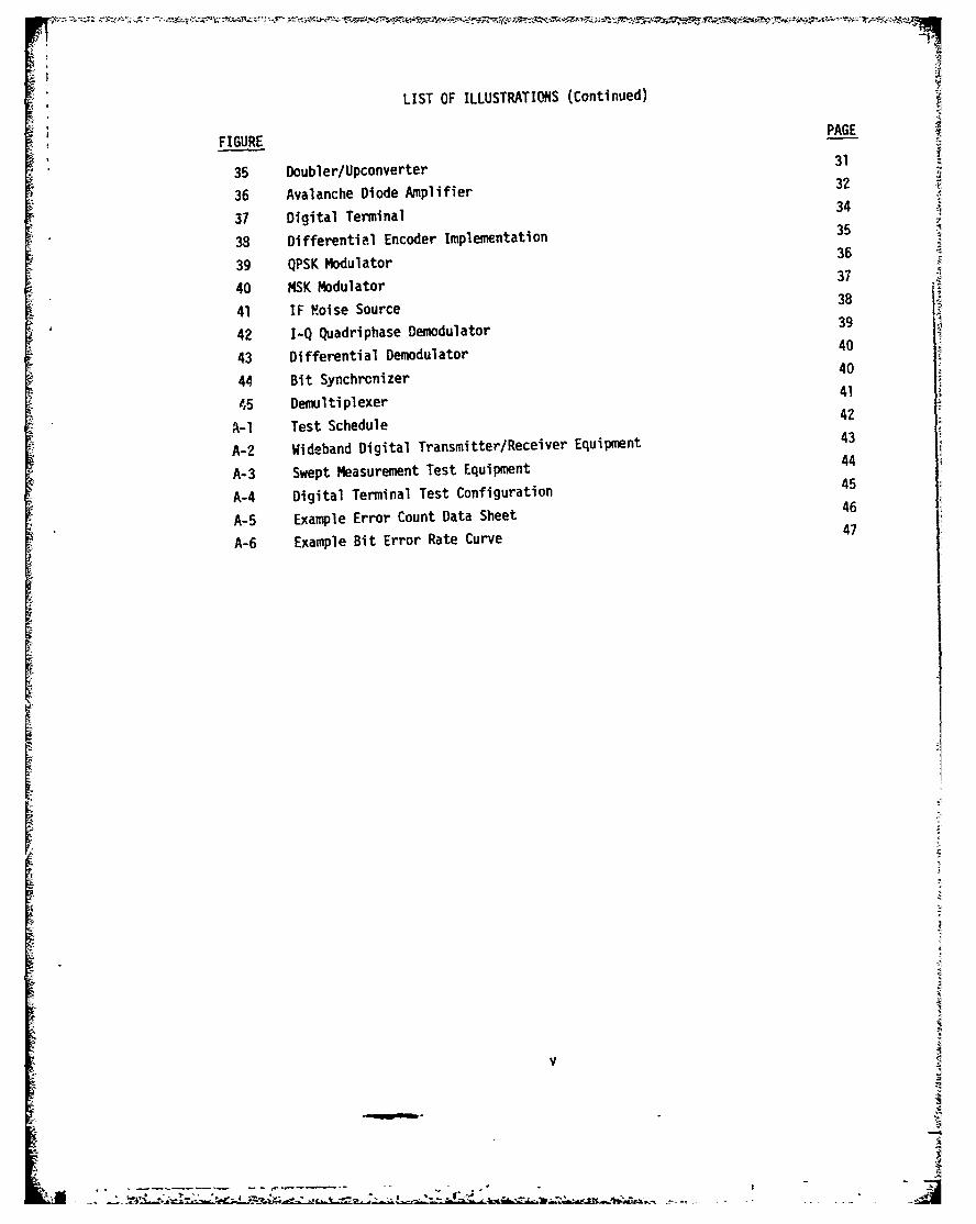
LIST OF ILLUSTRATIONS (Continued)
l PAGE
FIGURE PAGE
35 Doubler/Upconverter 31
36 Avalanche Diode Amplifier 32
37 Digital Terminal 34
38 Differential Encoder Implementation 35
39 QPSK Modulator 36
40 MSK Modulator 37
41 IF Moise Source 38
42 I-Q Quadriphase Demodulator 3943 Differential Demodulator 40
44 Bit Synchrcnizer 40
45 Demultiplexer 41
A-l Test Schedule 42
A-2 Wideband Digital Transmitter/Receiver Equipment 43
A-3 Swept Measurement Test Equipment 44
A-4 Digital Terminal Test Configuration 45
A-5 Example Error Count Data Sheet 46
A-6 Example Bit Error Rate Curve 47
IV
A2
v)
-- ~ I-

"LIST OF TABLES
TABLE PAGE
1 BER Performance Summary 2
2 Link Distortion Summary 3
3 MSK Digital Terminal Test Result Summary 7
4 QPSK Digital Terminal Test Result Summary 9
5 Differentially Coherent QPSK Digital Terminal Performance Summary 11
6 MSK Ka-Band Demonstration Link Performance Summary 16
7 QPSK Ka-Band Demonstration Link Performance Summary 20
8 Differentially Coherent QPSK Ka-Band Demonstration Link PerformanceSummnary 22
9 Performance Summary of the S-Band Frequency Source 30
10 Differential Encoder as a Function of Input Word 34
A-1 Link Passband Measurement Summary 44
A-2 Digital Testing Summary 48
vi
° - --,- - .. ..- o -

• [ " ' - - - - ---- I -
EVALUATION
New techniques for achieving improved bit error rates in high speeddigital links are of continuing interest. One such new technique isMSK modulation.
The purpose of this study was to determine the bit error rate performanceof both MSK and QPSK modulated signals. The tests were designed to evaluatethe suitability of each type of modulation for use in a 500 Mbps Ka-bandterrestrial link.
The use of MSK and QPSK, in a 500 Mbps Ka-band link has therefore,been demonstrated and the pLeuicted superior BER of MSK compared toQPSK has been confirmed.
LEWIS A. JAVARONEProject Engineer
4
Vii.

SECTION I
INTRODUCTION AND SUMMARY
This final report describes the results of a test program performed by TRW Defense
and Space Systems under contract No. F30602-76-C-0278, Iideband Digital Transmitter/Receiver, for the Air Force Systems Command, Rome Air Development Center. The period
of performance was 15 May 1976 through 25 March 1977. The purpose of the program was
to demonstrate the feasibility of a 500 Mbps digital link operating in the 36 to 38.6
GHz band.
Military requirements for digital communication links have steadily increased in
the previous years and are projected to continue doing so. In support of this predic-tion is the continuing trend to upgrade existing systems and to confit'ure new ones usingdigital modulation techniques. Future communication systems in the next decade are
predicted to became fully digital to take advantage of less cumulative noise degrada-
tion, greater flexibility of multiplexing, and adaptability to secure encryption.
The increasing amount of communications traffic is rapidly utilizing all of the
available bandwidth in the current frequency bands up through Ku-band. For this
reason future communication links are being configured to operate at higher and higherfrequencies. The 36 to 38.6 GHz band is currently being evaluated for digital use
because it offers the required bandwidths for high data rate links.
This program demonstrated the use of three different types of modulation for a
500 Mbps Ka-band link. The three types of modulation evaluated wiere coherent quadri-
phase shift keyed (QPSK), differentially coherent QPSK, and minimum shift keyed (MSK).To perform this tark, two sets of equipment were assembled. The first was a digital
terminal which served as both the data transmitter and receiver. The second was aKa-band demonstration link which simulated the degradation to the modulated signal
which occurs when the signal is transmitted through an actual 10 km Kd-band link.
The key parameter used to establish the performance of the link using each of the
three modulation formats was the bit error rate (BER). The testing was performed intwo phases. During the first phase, the BER of the digital terminal alone was measured.
The testing was then repeated by transmitting the modulated signal through the demon-
stration link. The results of these tests confirmed the predictions that MSK wouldoperate with the lowest overall BER and that of the two forms of QPSK, coherent would
be superior.
This investigation provided some of the basic data necessary to specify a modula-tion type for a Ka-band 500 Mbps data link. The relative BER performance of the three
candidate modulation types has been established. For systems in which the lowest
possible BER is required, MSK modulation should be used. For links with less stringent
BER requirements, ceherent QPSK would be optimum. And finally, fur systems with relaxedBER requirements, differentially coherent QPSK is a low cost alternative.
'~ - I
;'•. - -" •• . . . •- -.

• ,d' -:'. ---. .. . .,• '-• -- ' r• . ... --3' * ... --- - _
SECTION IIPROGRAM TEST RESULTS
The purpose of this program was to characterize the bit error rate (BER) performance
of a Ka-band link operating at a data rate of 500 Mbps. Three different types of modu-
lation were evaluated: minimum shift keying (MSK), coherent quadriphase shift keying
(QPSK), and differentially coherent QPSK.
To perform this task two sets of equipment were utilized. The first is a high data
rate digital terminal consisting of QPSK and MSK modulators, an IF noise source, demodu-
lator, bit synchronizer, data generator, and bit error rate counter. The second set ofequipment is the Ka-band demonstration link and consists of an S to Ka-band upconverter,a Ka-band avalanche diode amplifier (ADA), a Ka to S-band downconverter, and the appro-
priate local oscillators. This equipment is detailed in Section 3.
The testing was conducted in two phases. The first phase characterized the digital
terminal alone and the second phase characterized the combined terminal and demonstration
link. This sequence of testing was followed to separate the degradation resulting from
the modulator, demodulator, and bit synchronizer from the degradation due to the dis-
tortion in the link. The results of these tests and the computer simulated error rates
are summarized in Table 1. At a BER of 1 x 10⁻⁶, the differential degradation intro-
duced by the Ka-band link was 0.? dB for MSK, 0.7 dB for coherent QPSK, and 0.9 dB for
differentially coherent QPSK. The simulated degradation for MSK was 0.4 dB and 0.8 dB
for both forms of QPSK.
TABLE 1. BER PERFORMANCE SUMMARY
BER Degradation at Error Rate of 1 x 10⁻⁶
Differentially Coherent
Configuration MSK Coherent QPSK QPSK
IF back-to-back 0.5 dB 1.0 dB 3.0 dB
Ka-band demonstration 0.8 dB 1.7 dB 3.9 dBlink -measured
Differential degradation 0.2 dB 0.7 dB 0.9 dB
Computer simulateddifferential degradation 0.4 dB 0.8 dB 0.8 dB
2
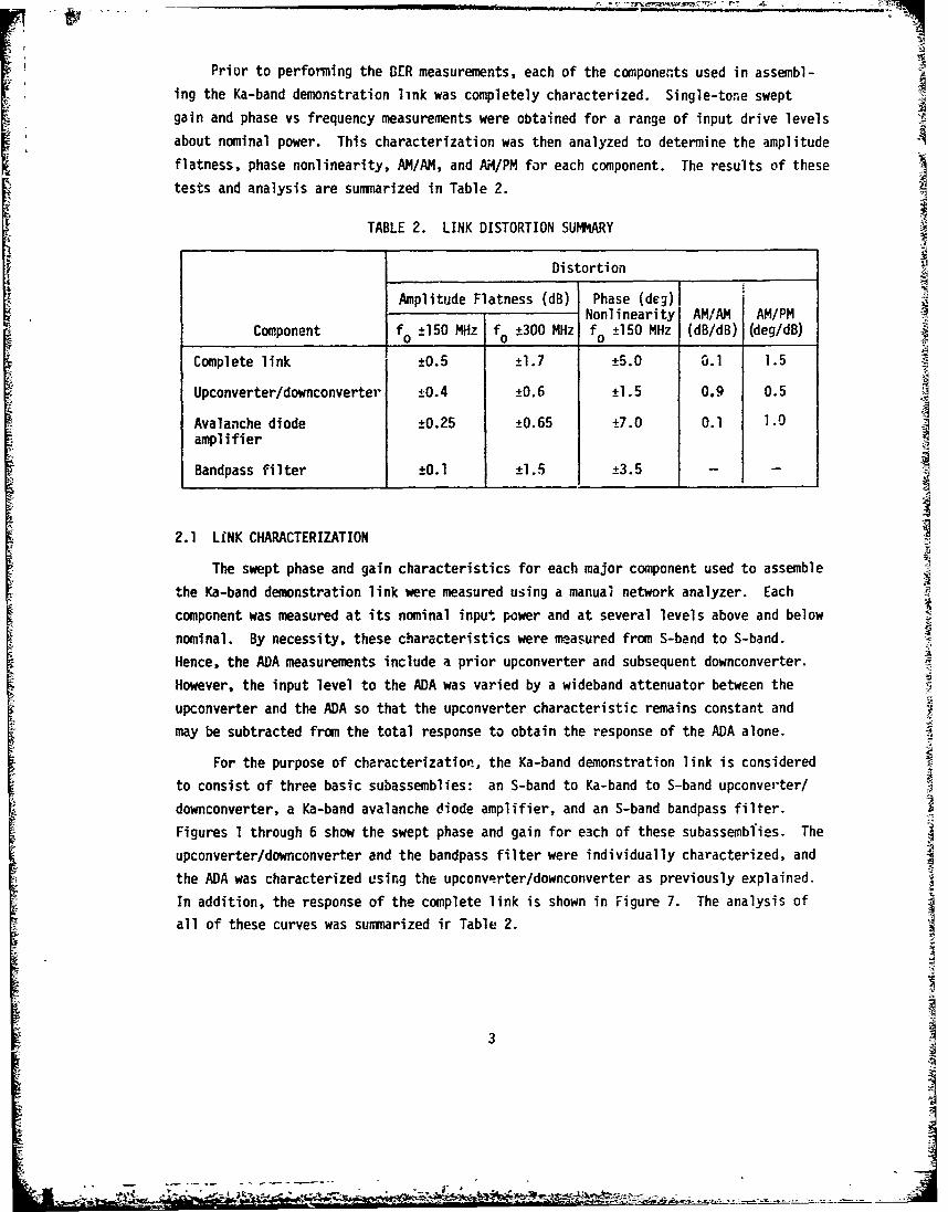
Prior to performing the DER measurements, each of the components used in assembl-
ing the Ka-band demonstration link was completely characterized. Single-tone swept
gain and phase vs frequency measurements were obtained for a range of input drive levels
about nominal power. This characterization was then analyzed to determine the amplitude
flatness, phase nonlinearity, AM/AM, and AM/PM for each component. The results of these
tests and analysis are summarized in Table 2.
TABLE 2. LINK DISTORTION SUMMARY
Distortion
Amplitude Flatness (dB) Phase (deg)
Nonlinearity AM/AM AM/PMComponent f 0 ±150 MHz f 0 ±300 MHz f 0 ±150 MHz (dB/dB) (deg/dB)
Complete link ±0.5 ±1.7 ±5.0 0.1 1.5
Upconverter/downconverter ±0.4 ±0.6 ±1.5 0.9 0.5
Avalanche diode ±0.25 ±0.65 ±7.0 0.1 1.0amplifier
Bandpass filter ±0.1 ±1.5 ±3.5 -
2.1 LiNK CHARACTERIZATION
The swept phase and gain characteristics for each major component used to assemble
the Ka-band demonstration link were measured using a manual network analyzer. Each
component was measured at its nominal input power and at several levels above and below
nominal. By necessity, these characteristics were measured from S-band to S-band.
Hence, the ADA measurements include a prior upconverter and subsequent downconverter.
However, the input level to the ADA was varied by a wideband attenuator between the
upconverter and the ADA so that the upconverter characteristic remains constant and
may be subtracted from the total response to obtain the response of the ADA alone.
For the purpose of characterization, the Ka-band demonstration link is considered
to consist of three basic subassemblies: an S-band to Ka-band to S-band upconverter/
downconverter, a Ka-band avalanche diode amplifier, and an S-band bandpass filter.
Figures 1 through 6 show the swept phase and gain for each of these subassemblies. The
upconverter/downconverter and the bandpass filter were individually characterized, and
the ADA was characterized using the upconvqrter/downconverter as previously explained.
In addition, the response of the complete link is shown in Figure 7. The analysis of
all of these curves was summarized ir Table 2.
3 •
bm 0

-50 -4W -300 -20 -100 fo Ow1 +wO +30 4400 4ml
FREQUENCY IMHZ
Figure 1. Ka-Band Upconverter/Downconverter Gain Variation
O 10
-4(X) -400 -300 -200 -100 fo -!100 +200 +300 4460 iemFREQUENCY (MHZ)
--.... ..... Figure 2. '(a-Band Upconverter/Downconverter Phase Nonlinearity
0
-4- _-
-5w -400 -30~ -200 -100 to +100 +200 +300 +440 Ow0
FREOUFNCYf (MHz)
Figure 3. Ka-Band ADA Gain Variation
44

A' _-,o ./-- - -
.-. /0
--Go -40 -a -200 -100 fo +100 +300 440 4W0
PRmOUINCY (WHO)
Figure 4. Ka-Band ADA Phase Nonlinearity
-10
10-/\,.- -- - -_~
-30 - -- - - - - -0 - - -
- - W -W -4 -4W -36 -200 -100 is. 4100--A 4m __4m 4PRIOUGNW (MHR)
Figure 5. Bandpass Filter Insertion Loss
+10
-10 •
+20- - _
Figure 6. Bandpass FilterPhase Nonlinearity
-- 30----40 -30 -200 -100 fo +100 +200 +300
FREQUENCY (MHO)
5
, -
S.. ..... *".. .••....-lf•. . .. ••• "••• • '': " .. ..... • ..... N%.___-,4'- . . .. . A-,:• • • ,,... .,,.z
FREQUENCY IMHZ)
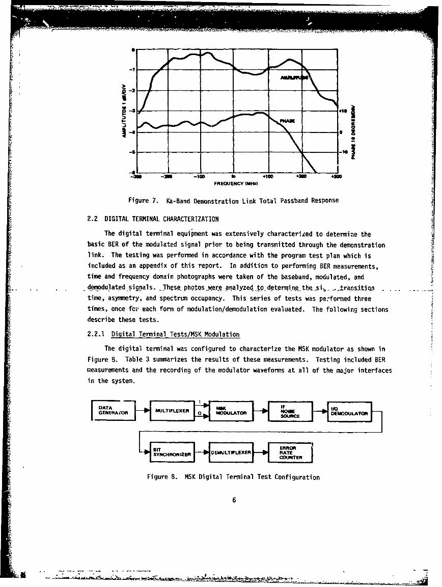
Figure 7. Ka-Band Demonstration Link Total Passband Response
4 -
2.2 DIGITAL TERMINAL CHARACTERIZATION
The digital terminal equipment was extensively characteriLed to determine thebasic BER of the modulated signal prior to being transmitted through the demonstrationlink. The testing was performed in accordance with the program test plan which isincluded as an appendix of this report. In addition to performing BER measurements,time and frequency domain photographs were taken of the baseband, modulated, and
demodulated signals. Jhes!e phrtos.e~r.q to lyzed tordetmittne tbe.hsiu thdransittion -
time, asymmetry, and spectrum occupancy. This series of tests was performed threetimes, once fc- each form of modulation/demodulation evaluated. The following sectionsdescribe these tests.
2.2.1 Digital Terminal Tests/MSK Modulation
The digital terminal was configured to characterize the MSK modulator as shown inFigure B. Table 3 summarizes the results of these measurements. Testing included BERm•easurements and the recording of the modulator waveforms at all of the major interfacesin the system.
"D BUIT L .X! OFMWLT NEowOrrEERROR
Figure 8. MSK Digital Terminal Test Configuration
i6
± .. "" -.. ... ... "'.. .. . ........- " "*-

TABLE 3. MSK DIGITAL TERMINAL TEST RESULT SUMMARY
Parameter Performance
BER degradation a*. 1 x lO-6 0.6 dB
Data asymmetry ±200 psec
BER Tests
R The BER performance of the MSK modulator was measured over an Eb/No range of 8 to
12 dB. This was sufficient to vary the resulting error rate frq.m >IO-4 to <1O- 7 . The
measured degradation from theotetlcal was a constant 0.6 dB over the full Eb/No range.I The complete BER curve is shown in Figure 9. The fact that the error rate did not
flair at high Eb/No values indicates that the complete system was properly operatingand that there were no anomalous sources of errors such as phase noise or improper tim-
ing in the bit synchronizer.
10
a 11 12 13 14
Figure 9. MSK Digital Terminal BER Performance
7
Ls

Spectrum Occupancy
The spectrum cccupancy of the MSK modulated signal was determined using a manual
spectrum analyzer. :igure 10 shows the RF output spectrum of the modulator. The
multiple nulls in the spectrum are due to multiplexing which occurs in the PRN seouence
generator and the skew between the I and Q channels. The first null in the MSK spectrum
occurs at 1.35 x the baud rate. Therefore, the first nulls occur at ±340 MHz (1.35 x
250 MHz), which is clearly seen in the photograph. In addition, the photograph shows
that all of the modulated energy outside the ±300 MHz link bandwidth is down by >25 dB
with respect to the maximum in-band level.0
-10
-20
10 +-< .... .. ..
FREQUENCY (MHz)
Figure 10. MSK Modulator Output Spectrum
Demodulated Waveforms
The waveforms at the output of the demodulator were recorded and analyzed to
determine the data asymmetry and overall quality of the signal. These photographs are
shown in Figure 11. The overview photograph shows 25 consecutive bits of the I and Q
channels, from which it is possible to see the cosinesoidal pulse shape of the demodu-
lated MSK waveform. The second photograph is an eye pattern and is useful in determin-
ing the asymmetry of the demodulated signal. The pattern is the sum of all of the bits
in the 127-bit PRN sequence. The width of the pattern at the zero crossing represents
the total asymmetry throughout the entire sequence and includes the effects of any
pattern sensitivity. For the MSK signal, the demodulated asymmetry is ±200 psec.
2.2.2 Digital Terminal Tests/Coherent QPSK Modulation
The second terminal configuration that was evaluated was coherent QPSK. The block
diagram of the terminal for these tests is sh qn in Figure 12. The results of these
tests are summarized in Table 4. Testing included BER measurements and the recording
of the modulator waveforms at all of the major interfaces in the system.
8

V]
TABLE 4. QPSK DIGITAL TERMINAL TEST RESULT SUMMARY
Parameter Performance
BER degradation at 1 x 10⁻⁶ 1.0 dB
Data transition time 500 psec
Data asymmetry J ±250 psec
b) Demodulated MSK Signal Eye Pattern
Figure 11. Digital Terminal Waveforms
0M ERACA
Figure 12. Coherent QPSK Digital Terminal Test Configuration
q

BER Tests
The BER performance of the QPSK modulator, as shown in Figure 13, was measured
over a~n Eb/No range of 8 to 14 dB. This range was sufficient to vary the resulting
error rate from >10- to <10-, The measured degradation from theoretical was 1.0 dB
at an error probability of 1 x 10⁻⁶ and increased to 1.4 dB at an error probability of
1 x 10-. The slight increase in error rate is due to the finite imperfections in the
bit synchronizer timing.
-4
0
0 -88 11l 10 11 12 13 14
Figure 13. Coherent QPSK Digital Terminal BER Perform
Spectrum Occupancy
The spectrum occupancy of the QPSK modulated signal was determined using a manual
spectrum analyzer. Figure 14 shows the output spectrum of the modulator. The first
nulls of the spectrum envelope are at ±_250 MHz (1 x baudrate). The extra nulls in the
spectrum are due to the correlation between the I and Q channels. From the photo it
can be seen that there is still significant energy outside the +_3G0 MHz link bandwidth.
The maximum level outside the band is 15 dB below the in-band peak compared to >25 dB
for MSK.10

r i . ." .
0
~j4 -10
-40t.
IL
4W -200 +200 44W
FREQUENCY (MHz)
Figure 1$. Coherent QPSK Modulator Output Spectrum
Demodulated Waveforms
The waveforms at the output of the demodulator were recorded and analyzed to deter-
mine the 10 to 90% transition time, data asymmetry, and overall quality of the signal.
These photographs are shown in Figure 15. The overview photograph shows 25 consecutive
bits of the I and Q channels. The transition time photo is a double exposure of both
the rise and fall time of a typical bit. The typical demodulated 10 to 90% transition
time was 700 psec. Assuming equal contributions for both the modulator and demodulator
and that the measured transition time is the rms value of the two, the calculated mod-
ulator transition time is 500 psec. The final photograph is the eye pattern for the
demodulated QPSK signal. Analysis of this photo indicates that the maximum asymmetry
throughout the code is ±250 psec.
2.2.3 Digital Terminal Tests/Differentially Coherent QPSK Modulation
The third and final terminal configuration evaluated was differentially coherent
QPSK. The block diagram of the terminal for these tests is shown in Figure 16. The
results of these tests are summarized in Table 5. Testing included BER measurements
and the recording of the modulator waveforms at all of the major interfaces in the
system.
TABLE 5. DIFFERENTIALLY COHERENT QPSK DIGITALTERMINAL PERFORMANCE SUMMARY
Parameter Performance
BER degradation at 1 x 10"6 3.0 dB
Data transition time 330 psec
Data asymmetry ±250 psec
11

a) QPSK Waveforms
b) QPSK Rise and Fall Times
C) QPSK Signal Eye Pattern
Figure 15. Digital Terminal Demodulatcd Waveforms
12
- - - -
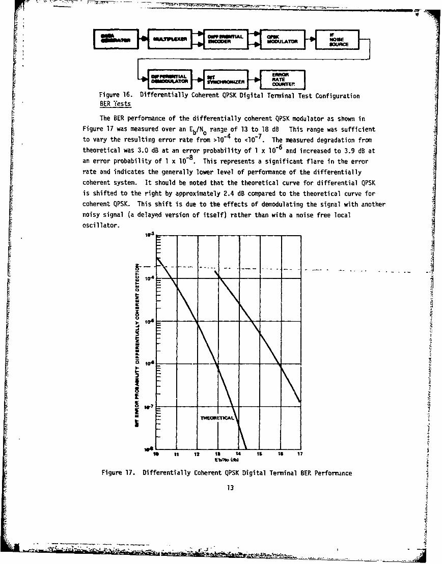
i ~ Figure 16. Differentially Coherent QPSK Digital'Terminal Test Configuration •
.BER YestsMU'
to vary the resulting error rate from >lh-e to <10-D . The measured degradation from
theoretical was 3.0 dB at an error probability of 1 x 10⁶ and increased to 3.9 dB at
an error probability of I x 10-8. This represents a significant flare in the errorrate and indicates the generally lower level of performance of the differentially
coherent system. It should be noted that the theoretical curve for differential QPSKis shifted to the right by approximately 2.4 dB compared to the theoretical curve forcoherent QPSK. This shift is due to the effects of demodulating the signal with anothernoisy signal (a delayed version of itself) rather than with a noise free local
oscillator.
Io-
log
--- 4Ii
THEORErCAL
S Is 12 Is 14 is Is 17EbI/o W
Figure 17. Differentially Coherent QPSK Digital Terminal BEP Performance
13
**~* **** .. .- ~ ~ -

Spectrum Occupancy
The spectrum occupancy of the differentially coherent QPSK signal was determined
using a manual spectrum analyzer. Figure 18 shows the RF output spectrum of the
modulator. The spectral line spacing for the differentially encoded QPSK is 492 kHz
vs 1.968 MHz for QPSK and MSK tests. This is because the differential encoding
increases the PRN code length from its normal value oi 127 bits by a factor o• 4 to 508
bits. The differential encoding does not affect the other spectral occupancy param-
eters. The first nulls for the spectrun, remain at ±250 MHz (1 x the baud rate). As
with coherent QPSK, there is significant energy outside the ±300 MHz link bandwidth.
0
-10 .÷.-
S-•:. '- . •..
o I . ° S
-2D r
-30
4W -W4200 4400
FREQUENCY (MHz)
Figure 18. Differentially Coherent QPSKModu.aton .....
S...........-. ............. Output SpoctrdihDemodulated Waveforms
The waveforms at the output of the demodulator were recorded and analyzed to
determine the T0 to 90% transition time, data asymnetry, and overall quality of the
signal. These photographs are shown in Figure 19. The overview photograph shows 25
consecutive bits of the I and Q channels. From the photo, it is evident that there is
considerably more distortion on the demodulated waveform compared to coherent QPSK
(refer to Figure 15a), particularly in the sequence of seven consecutive l's. This
higher level of distortion is due to the fact that the power level of both input sig-
nals to the demodulator phase detectors are continuously changing compared to coherent
QPSK which utilizes a constant amplitude local oscillator.
The transition time of the demodulated signal was improved by the differential
encoding at the expense of significant overshoot in the transition. The calculated
value assuming a demodulator rise time of 500 psec was 330 psec. The improvement in
risetime is due to the fact that both inputs to the demodulator are simultaneously
changing and result in a higher dv/dt at the phase detector. The asymmetry of the
differentially encoded signal was degraded. Analysis of the demodulated eye pattern
shows the asymmetry to be ±350 psec compared to ±250 psec for coherent QPSK. This
effect is also the consequence of not using a stable local oscillator to demodulate
the signal.14
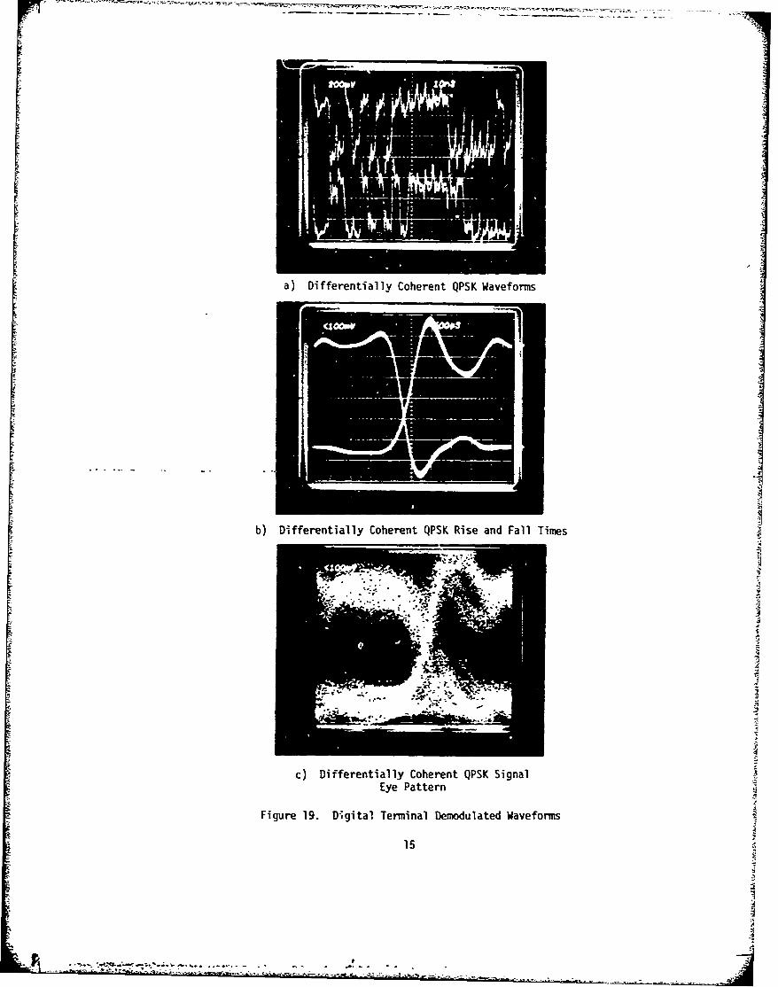
a) Differentially Coherent QPSK Waveforms
b) Differentially Coherent QPSK Rise and Fall Times
c) Differentially Coherent QPSK SignalEye Pattern
Figure 19. Digital Terminal Demodulated Waveforms
15

2.3 COMBINED DIGITAL TERMINAL/Ka-BAND LINK TESTS
The final phase of this program was the testing of the complete system. This
series of tests served two purposes: first to determine the BER of the total system,
and second, when the results of these tests are compared to the performance of just
the digital terminal, it is possible to determine the incremental degradation intro-
duced by the Ka-band link. The same basic test philosophy employed to characterize
the digital terminal alone was followed in this set of tests. The testing was per-
formed in accordance with the program test plan (refer to the appendix). In addition
to performing BER measurements, time and frequency domain photographs were taken of the
modulated and demodulated signals. These photos were analyzed to determine the signal
transition time, asymmetry, and spectrum occupancy. This series of tests was performed
three times, once for each form of modulation/demodulation being evaluated. The follow-
ing sections describe these tests.2.3.1 Demonstration Link Tests/MSK Modulation
The digital terminal and demonstration link were configured as shown in Figure 20
to characterize the BER of the system using MSK modulation. The results of the testing
are su'mmdrized in Table 6. Testing included BER measurements and photographing of the
modulated and demodulated waveforms.
TABLE 6. MSK Ka-BAND DEMONSTRATION LINKPERFORMANCE SUMMARY
Parameter f Performance
BER degradation at 1 x 10⁻⁶ 0.8 dB
Data asmnimetry ±200 psec
GENERAT(; 11LT11LEXE MODULATOR TO
IFIFigure 20. MSK Demonstration Link Test Confiouration
"16
......- 2

BER Tests j
The BER performance of the Ka-band link using MSK modulation was measured over an
Eb/No range of 8 to 13 dB. This was sufficient to vary the resulting bit error rate
from >10-4 to <l0- 7 . The measured degradation from theoretical was 0.8 dB at an error
rate of 10-6, and increased to 1.0 dB at 5 x 10⁻³. The slight increase in BER is due
to the effects of noise in the Ka-band link. The complete BER curve is shown in
Figure 21.10-3_
107
I-J
THEORETICAL
L A
S 9 10 11 12 13 14
Figure 21. -Band Demonstration Link -SK BER Performance
The net increase in system BER due to the Ka-band link was only 0.2 dB. Although€
this result is low it is consistent with the known properties of MSK. Two factors con-
tribute to the excellent performance: first, the link bandwidth is sufficient to trans-
mit >99% of the MSK signal energy, and second, the phase and amplitude distortions in
the link passba.nd is minimal.
17
L~

The demonstration link i.as configured so that it was possible to bypass the ADA.
This made it possible to measure the performance of the link with and without the ADA.
The result of the test was that the ADA improved the BER of the system by 0.15 dB. This
result is consistent with the computer simulations of the link. The improvement is due
to the saturation in the ADA which reduces the residual AM on the MSK signal and there-
fore improves the BER. The remainder of the link components are all operated in a
linedr mode, and therefore do not contribute to this effect.
Utilization of saturated amplifiers is a common technique in phase modulated sys-
tems and must be carefully controlled to achieve the desired performance improvement.
There are two key parameters to control when using saturated amplifiers: passband shape
variation vs input level, and AM/PM. The Ka-band ADA utilized in these tests was
carefully aligned to optimize both of these parameter:. In addition, these parameters
must be controlled over the full bandwidth of the modulated signal. As will be dis-
cussed in Se!ction 2.3.2, in the case of the QPSK testing, the saturated ADA degraded
-the link performance. T1,is Was because the bandwidth of thi QPSK modulated signal'.....
exceeded the bandwidth of the ADA. Thus, the signal suffered a net degradation when
transmitted through the ADA.
-Spectrum Occupancy
A photograph of the spectrum occupancy of the MSK waveform after being transmitted
through the complete Ka-band demonstration link is shown in Figure 22. Compared to the
MSK spectrum recorded directly at the output of the modulator (refer to Figure 10),
there is very little visible distortion to the modulated spectrum. The only effect
was a slight distortion in the top of each lobe. The one result of being transmitted
through the link that is quite evident is the bandlimiting which has occurred. There
' no detectable signal energy outside the ±300 MHz link bandwidth.
0
-10
-20
30
~-60 lod( T
-00+200 +400
FREQUENCYN(HzI
Figure 22. MSK Modulated Signal Spect~rum at Output ofKa-Band Demonstration Link
18

Demodulated Waveforms
The waveforms at the output of the demodulator were recorded and analyzed todetermine the data asymmetry and overall quality of the signal. These photographs areshown in Figure 23. The overview photograph shows 25 consecutive bits of the I and Qchannels. This photo shows the effect of the link bandlimiting on the demodulatedwaveform. Each pulse should return to the 50% point, but the bandlimiting preventsthis. This form of degradation is not particularly severe because it does not signifi-cantly affect the peak value of the signal after it has been integrated prior to thedecision process.
The second photograph is the demodulated eye pattern of the signal. Analysis ofthis photograph indicates that the asymmetr-y is ±200 psec, which is unchanged from thevalue measured directly at the output of the modulator.
,,on-
a) MSK Demodulated Waveforms
b) MSK Demodulated Signal Eye Pattern
Figure 23. Signals After Transmission Through theKa-Band Demonstration Link
19
†††††††††††

2.3.2 Demonstration Link Tests/Coherent QPSK Modulation
The digital terminal and demonstration link were configured as shown in Figure 24
to characterize the performance of a system using coherent QPSK modulation. The results
of these tests are summarized in Table 7. Testing included measuring the BER and
photographing the modulated and demodulated waveforms.
TABLE 7. QPSK Ka-BAND DEMONSTRATION LINKPERFORMANCE SUMMARY
Parameter Performance
BER degradation at 1 x 10⁻⁶ 1.7 dB
Data transition time 1.9 nsec
Data asymmetry ±500 psec
D A.. . T A " " " IEX HGENERATOR IJLILXR IU.~m
ERROR
DEMOOUAD • RATE~ON•
Figure 24. Coherenc QPSK Demonstration Link Test Configuration
BER Tests
The BER performance of the Ka-band link using coherent QPSK modulation was
measured over an Eb/No range of 9 to 14 dB. This was sufficient to vary the resulting
bit error rate from >l0-4 to <10-7. The measured degradation from theoretical was
1.7 dB at an error rate of l10 and increased slightly to 1.9 dB at 5 x 10⁻⁸. The
complete BER curve is shown ;n Figure 25. The incremental BER degradation of the
system due to the Ka-band link was 0.7 dB. As was expected, this result is higher than
the 0.2 dB measured for MSK and reflects the level of improvement available in link
performance by using MSK over QPSK.
The BER testing of the link was repeated with the ADA bypassed to determine its
effect on the link BER performance. With the ADA bypassed, the BER degradation was
1.7 dB compared to 1.9 dB with the ADA in the link. This result is just the reverse
of what was found for MSK and is indicative of the lower tolerance of QPSK to link
distortion.
20
__

#3~
E
0
10-7
a 8 10 11 12 13 14
SFigure 25. Ka-Band Demonstration Link Coherent QPSK BER Performance
S~Spectrum Occupancy
SThe photograph of the spectrum occupancy of the coherent QPSK modulated signal
after being transmitted through the complete Ka-band demonstration link is shown in
Figure 26. Compared to the coherent QPSK spectrum recorde directly at the output of
the modulator (refer to Figure 14), there is little visible distortion to the modulated
spectrum, other than a slight distortion in the tops of the energy lobes which fall on
the skirts of the bandpass filter. The effect of the limited link bandwidth is appar-
Sent fmq the photo. After being transmitted through the link, the modulated energy
levels at fo ±450 M•z have been reduced from the unfiltered level of 20 dB below thepeak level to >40 dB down.
Demodulated Waveforms
The waveforms at the output of the demodulator were recorded and analyzed to
determine the demodulated transition time, data asymmetrv, and overall quality of the
M21
S 3

V -- e,
.20
i-30 1
,(~-40-W l
- 4 -200 10 .200 0
FREQUENCY (MHz)
Figure 26. Coherent QPSK Modulator Spectrum after TransmissionThrough the Ka-Band Demonstration Link
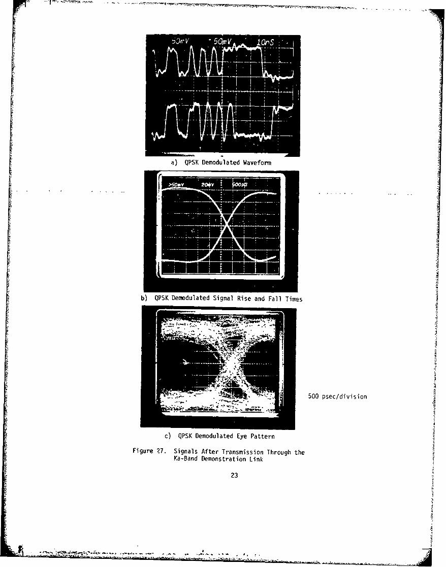
signal. These photographs are shown in Figure 27. The overview photqgraph shows ?5
consecutive bits of the I and Q channels. The photo shows the increase in data transi-tion time due to the link bandlimiting and the elimination of overshoot following
transition due to saturation in the ADA.
The second photograph shows the demodulated transition times for the signal. Thetypical 10 to 90% transition time was 1.9 nsec, which is signficantly degraded from the
700 psec value measured directly at the output of the modulator. The final photograph
is the eye pattern for the demodulated signal. Based on this photo, the worst caseasymmetry is ±500 psec, compared to ±250 psec measured directly at the modulator output.
The asymmetry degradation is due to the link nonlinearities which distort the shape ofthe bits, as a function of the data sequence. That is, a field of successive 1, 0, 1, 0
transitions will have higher asymmetry than a field of successive l's or O's. This
effect can be seen in the overview photograph.
2.3.3 Demonstration Link Tests/Differentially Coherent QPSK Modulation
The digital terminal and demonstration link were configured as shown in Figure 28
to characterize the performance of the system using differentially coherent QPSK modu-
lation. The results of these tests are ;ummarized in Table 8. Testing included mea-suring the BER and photographing the modulated and demodulated waveforms.
TABLE 8. DIFFERENTIALLY COHERENT QPSK Ka-BAND DEMON-STRATION LINK PERFORMANCE SUMMARY
Parameter Performance
BER degradation at l x 106 3.9 dB
Data transition time 1.2 nsec
Data asymmetry ±600 psec
22
" " .. -"r
a) QPSK Demodulated Waveform
b) QPSK Demodulated Signal Rise and Fall Times
VF:500 psec/division
c) QPSK Demodulated Eye Pattern
Figure 27. Signals After Transmission Through theKa-Band Demonstration Link
23

IFNOISE DIFFERENTIAL RSOURtCE DEIOOULAT0A SNHOiERRA
Figure 28. Differentially Coherent QPSK Demonstration Link Test Configuration
BER Tests
The BER performance of the Ka-band link using differentially coherent QPSK modula-
tion was measured over an Eb/No range of 13 to 19 dB. This was sufficient to vary the
resulting error rate from >l- to <l0-7. The measured degradation from theoretical
was 3.9 dB at an error rate of 10-6. The complete BER curve is shown in Figure 29.
The incremental BER degradation of the system due to the Ka-band demonstration
link was 0.7 dB. This is the same result as was achieved for coherent QPSK and indi-
cates that both forms of'QPSK a*e equally degradced'by'the link distortions.- It shoud.
be pointed out though that differentially coherent QPSK operates at an overall higher
z
I -w o5-__- - -\
:• hEORETI•AL
10 11 12 12 14 15 161 17
• Figure 29. Ka-Band Demonstration Link Differentially
S~Coherent QPSK BER PerformanceV24
.. '. *~z ~ ~ I0

error rate compared to coherent QPSK. Differentially coherent QPSK requires an Eb/No
of 16.9 dB to achieve an error rate of 10.6 whereas coherent QPSK requires only 12.4 dB.
The BER testing of the link was repeated with the ADA bypassed to determine its
effect on the link performance. With the ADA bypassed, the BER degradation increased
to 4.6 dB, compared to 3.9 dB with the ADA. The BER improvement by the ADA is primar-
ily due to saturation in that device.
The differentially encoded QPSK signal has significant AM on the waveform (100% at
transition). ihis AM introduces significant distortion in the demodulated data due
to the fac't that the demodulato- is both a phase and amplitude detector. Although the
ADA does introduce passband distortion in addition to limiting the signal, the net
result is to improve the link performance by 0.7 dB.
Spectrum Occupancy
The spectrum occupancy of the Differentially coherent QPSK modulated signal after
being transmitted through the complete Ka-band demonstration link is shown "'in Figure 30.
All modulated energy outside of the ±300 MHz link bandwidth is >25 dB down compared to
only 15 dB as measured directly at #-he modulator output. As previously explained in
Section 2.2.3, the lines in the spectrum do not follow a sin x/x distribution because
the differential encoding results in a data sequence which is no longer a maximal
length PRN code.
0
-40ww
,60I-.
-40 D -200 +200 4 40
FREOUENCY (MHz)
Figure 2-30. Differentially Coherent QPSK ModulatedSpectrum After Transmission Throughthe Ka-Band Demonstration Link
25
S. . -. . • ,• . . . .
Demodulated Waveforms
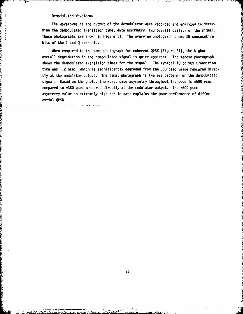
The waveforms at the output of the demodulator were recorded and analyzed to deter-mine the demodulated transition time, data asymmetry, and overall quality of the signal.
These photographs are shown in Figure 31. The overview photograph shows 25 consecutive
bits of the I and Q cnannels.
"When compared to the same photograph for coherent QPSK (Figure 27), the higher
overall degradation in the demodulated signal is quite apparent. The second photograph
shows the demodulated transition times for the signal. The typical 10 to 90% transition
time was 1.2 nsec, which is significantly degreded from the 300 psec value measured direc-
tly at the modulator output. The final photograph is the eye pattern for the demodulated
signal. Based on the photo, the worst case asymmetry throughout the code is ±600 psec,
compared to ±350 psec measured directly at the modulator output. The ±600 psec
asymmetry value is extremely high and in part explains the poor performance of differ-
ential QPSK.
26
2-4

a) Differentially Coherent QPSK Demodulated Waveforms
mI
b) Differentially Coherent QPSK Rise and Fall Times
4r V.
c) Differentially Coherent QPSK Eye Pattern "J
Figure 31. Differentially Coherent QPSK After TransmissionThrough the Demonstration Link A
27
LP --.

SECTION III
HARDWARE DESCRIPTION
Two sets of equipment were assembled to perform this test program: a Ka-banddemonstration link and a digital terminal. Both of these items were configured usingcommercial test equipment and special circuits and components designed by TRW. Thissection describes these components in detail.
3.1 KA-BAND DEMONSTRATION LINK DESCRIPTION
The Ka-band demonstration link includes all of the equipment (with the exceptionof antennas) necessary to completely simulate an actual data link. The link accepts awideband (600 MHz) S-band input and translates it to Ka-band (38 GHz). The signal isthen amplified to an output level of 100 mW. After attenuation to simulate path loss,
the signal is downconverted back to S-band, where it is then demodulated in the digitalterminal. The demonstration-link-consists of five major-subassemblies:
9 S-barnd frequency sources
e X9 multiplier/avalanche diode oscillator
e Doubler/upconverter
e Avalanche diode amplifier
e Downconverter.
Each of these components is discussed in detail in the following sections. The completedemonstration link is shown in Figure 32.
DOUBLERARCONVERUR AVALANCHE DIODE AMPLIFIER
SIGNA BANOPASS OUJTPUTINPUT UCFLE
PUMP SOURCE
Figure 32. Ka-Band Demonstration Link
28

3.1.1 S-Band Frequency Sources
Two S-band frequency sources are used in the demonstration link. The first (2.144
GHz) serves as the carrier source to the modulator. The second serves as the input to
the S to Ka-band frequency multiplier chain. The sources utilize space-qualified elec-
trical and mechanical design concepts which incorporate mechanically standardized alum-
ina microstrip modules. A photograph of one of the sources is shown in Figure 33.
Figure 33. S-Band Frequency Source
Conceptually, the S-band sources consist of a stable crystal oscillator followed bylow order frequency multipliers, interstage amplifiers, and filters. A total multipli-
cation factor of 24 is achieved using three successive multiplier stages: X2, X2, andX6. The pump source has a final output frequency of 2.063 GHz and provides an output
level of ±25 dBm. Table 9 summarizes its performance. The carrier source is similarto the pump source. The only difference is that the final output frequency is 2.144GHz and the output power level is +10 dBm.
3.1.2 X9 Multiplier •
The X9 multiplier consists of a single-step high order varactor diode multiplier
followed by an injection-locked avalanche diode oscillator (ADO). An output power levelZ
of +23 dBm is achieved at 18.077 GHz. A photograph of the multiplier is shown in Fig-I
ure 34. V
The X9 multiplier consists of an S-band input matching network mounted in a rec-tangular cavity located on top of the waveguide mount containing the varactor diode.
The output from the diode, which is mounted in reduced height waveguide, is passedthrough an impedance transformer into a separate waveguide output filter. Idler tuning
29
to - 0

TABLE 9. PERFORMANCE SUMMARY OF THE S-BANDFREQUENCY SOURCE
Parameter Performance
Output frequency 2.06333 GHz
Output power +25 dBm
DC power 200mAat 15 V*
3.0 watts
DC to RF efficiency 10.5%
Spurious output 22 dBc for 2nd harmonic50 dBc for 4th harmonic
>70 dBc for all other frequencies
Includes an integrated voltage regulator.
Figure 34. X9 Multiplier/Avalanche Diode Oscillator
is obtained by the introduction of waveguide shims between the flanges connecting thediode mount and the output filter. A coaxial lowpass filter is used to couple theinput signal to the multiplier diode.
The X9 multiplier drives an injection-locked avalanche diode oscillator. Theoscillator circuit utilizes a 0.020" high, reduced height waveguide, with double steptransformers to full height o'jtput waveguides. A triple screw tuner with X /4 screw
gspacings is located in the full height guide for RF tuning. Fabrication of the wave-guide diode mount was similar to the multiplier diode mount. The bias circuit was con-
30
S-J

structed as a length of coaxial air line bolted to the body of the waveguide. A five-
port waveguide circulator is used to couple the multiplier to the injection-locked
oscillator and to provide isolation between the multiplier/oscillator and oscillator
output interfaces. The inj^ction-locked ADO has an output power of +23 dBm at 18.077
GHz.
3.1.3 Doubler/Upconverter
The doubler/upconverter combines the functions of a frequency doubler and an
upconverter into a single circuit. The pump frequency (18.077 GHz) is doubled and
combined with the signal (2.144 GHz) using a parametric varactor diode circuit. The
resulting output frequency is %o = 2fPUMP - f signal* The correct output frequency is
selected by a multisection waveguide filter on the output port. The pump input port
also has a filter which pre~ents the upconverted output signal from propagating out the
pump port. The module, as shown in Figure 35, is constructed with an electroformed
cruciform structure in which the input and output waveguides are Ierpendicular to each
other. This type of construction allows each port to be optimized with a minimum of
interaction with the other port. The modulated carrier is injected into the GaAs
varactor diode via a combination lowpass filter and matching section mounted at the
intersection of the two waveguides and is perpendicular to the plane of the waveguides.
The combined doubler/upconverter results in fewer component parts and amore efficient
system because a doubler/upconverter has less conversion loss than a doubler followed
by an upconverter.
Figure 35. Ooubler/Upconverter
31

3.1.4 A'alanche Diode Amplifier
The output amplifier in the link (Figure 36) is a two-stage circuit using avalanche
diodes in a negative ,esistance mode. The negative resistance amplifier is a one-port
device in which the input and output signals coexist within one transmission line. In
order to obtain a useful amplifier, separate input and output ports are created using
a waveguide circulator. The circulator directs the input signal iiito the amplifier and
couples the amplified output signal to the output port.
2 JS. _
~11-
13
II J
.i5 35.5 36 36.5 31 37.5 38.0 38.5 39.0 39.$ 43.0
FIRIQQtICY 1k GI•
Figure 36. Avalanche Diode Amplifier
The ADA cansists of two separat-, amplifier modules series-coupled by a five-port
(three-junction) circulator. rhe modules utilize silicon Impatt diodes mounted in a
0.20" reduced heiqht waveguide. The mounts, which must function as high quality neat
sinks, are machined out of tellurium copper in a split block configuration. Electro-
formed quarterwave step transformers couple the mount to the circulato~-. Completing
the assembly are dc current regulators, one for each diode.
The individual stages within the Ka-band ADA exhibit characteristics found in
lower frequency multistage power amplifiers. The first stage amplifies the low inputleve'i (0 dBm) with high gain (12 dB). The output level (+20 dBm) is provided by the
second stage but with reduced gain (8 dB). The ADA operates in saturation (5:1 signal
compression) and requires 10 watts of dc power (145 mA at 26 volts and 230 mA at 27
volts), excluding power dissipated in thea current regulators.
3.1.5 Ka-Band Downconverter
The final assembly in the demonstration link is the Ka-band downconverter. Ii
consists of a Ku to Ka-band doubler, a balanced mixer downconverter, and an S-band
bandpass filter.32
10

The construction of the doubler is very similar to the doubler/upconverter. The
Ka-band doubler Is a cruciform waveguide structure with the input and output waveguides
perpendicular to each other. The GaAs varactor diode is mounted at the intersection of
the waveguides. The diode is self-biased using an external resistor network which is
RF decoupled from the varactor with a lowpass filter. The input end out1 dt ports ofthe doubler have tuning screw matching networks and bandpass filters.
The downconverter mixer is a standard commercial component. The mixer (Spacekcom
PN C37-2.4) downconverts the 38.299 GHz input signal to 2.144 GHz using the 36.155 GHz
local oscillator output from the doubler. The final component in the downconverter is
a bandpass filter. The filter is a commercial tubular design and sets the overall link
bandwidth.
3.2 DIGITAL TERMINAL DESCRIPTION
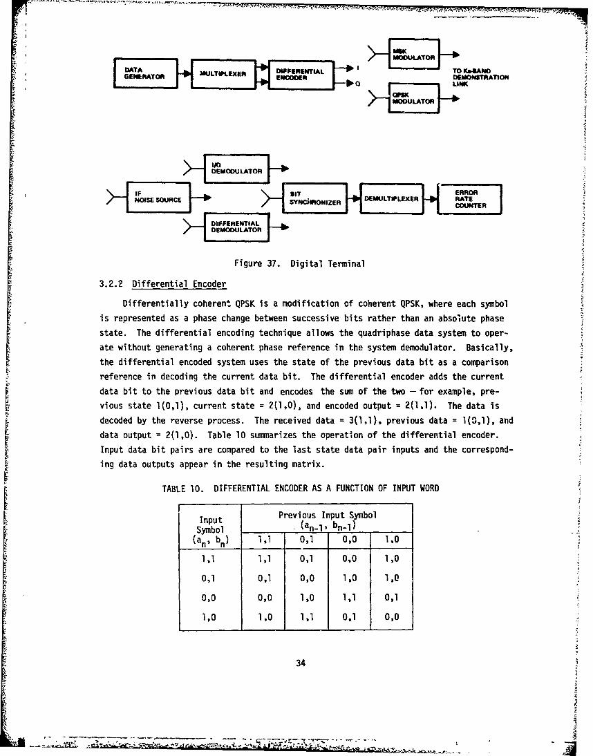
The digital terminal (Figure 37) served as both the source of the input signal to
the demonstration link and as the data receiver. Although the test set was configured
to operate at 250 Mbps per channel, it is capable of performing BER measurements cL data
ratec of up to 600 Mbps per channel (1.2 Gbps QPSK or MSK) and consists of the follow-
ing equipment:
* Tau-Tron PRN code data generator
* Multiplexer
* Differential encoder
* QPSK and MSK modulators
* IF noise source
a I-Q demodulator
6 Differential demodulator
* Bit synchronizer
* Demultiplexer
* Tau-Tron error rate counter.
3.2.1 Multiplexer-7
The multiplexer accepts the single 2 - 1 PRN code from the Tau-Tron generator
and creates separate I and Q channels. In addition, the multiplexer is used to double
the 100 to 300 Mbps data rate of the generator when required. The multipl .er generates
two channels by dividing the input data stream. One-half is amplified and becomes the
I channel. The other half is inverted and delayed by 2 bits and serves as the Q channel.
Finally, both data streams are reclocked to ensure low data asymmetry.
33
MODUATO
LINK":•' •I•I~lMODULATORI
OEM()U LDATOR
IF BIT ERRORNOISE SOURCE rYCI DZER MULTIPLEXER RA~TE
DODEMOOU LATOR
Figure 37. Digital Terminal
3.2.2 Differential Encoder
Differentially coherent QPSK is a modification of coherent QPSK, where each symbol
is represented as a phase change between successive bits rather than an absolute phase
state. The differential encoding technique allows the quadriphase data system to oper-
ate without generating a coherent phase reference in the system demodulator. Basically,
the differential encoded system uses the state of the previous data bit as a comparison
reference in decoding the current data bit. The differential encoder adds the current
data bit to the previous data bit and encodes the sum of the two - for example, pre-
vious state 1(0,1), current state = 2(1,0), and encoded output = 2(1,1). The data is
decoded by the reverse process. The received data = 3(l,l), previous data = 1(0,1), and
data output = 2(1,0). Table 10 summarizes the operation of the differential encoder.
Input data bit pairs are compared to the last state data pair inputs and the correspond-
ing data outputs appear in the resulting matrix.
TABLE 10. DIFFERENTIAL ENCODER AS A FUNCTION OF INPUT WORD
Input Previous Input Symbol
Symbol (an_,, bn-. )(an, bn) ,l Ol 0,0 1,0
l ill O11,1 0,0 1,0
O*l Ol 0,0 1,0 1,0
0,0 0,0 1,0 1,l 0,1
1,0 1,0 ,ll 0,1 0,0
34

The differential encoder has been implemented with the logic flow diagram shown
in Figure 38. Basically the logic state of the previous output is fed back to the
input NOR g.tes. This results in the desired phase change referenced data coding.
&6c
Figure 38. Differential Encoder Implementation
3.2.3 QPSK Modulator
The QPSK modulator is a standard parallel configuration as shown in Figure 39.
The 2.144 GHz carrier is split ii•to two equal amplitude quadrature channels by a 900hybrid. Each of the two channels is then biphase (00 and 1800) modulated by the input
data. The output of the two modulators is in-phase power combined to generate the
quadriphase modulated output signal. All of the modulator components are standard
commnercial items with the exception of the data amplifiers. The data amplifiers are
a TRW design which utilizes microwave transistors in order to obtain switching speeds
S~35
~~dn- 1 z 0~. - -
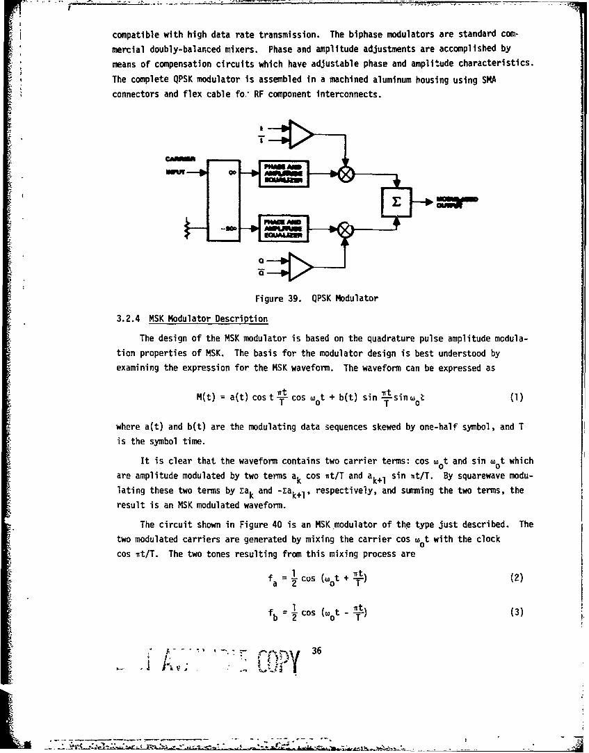
compatible with high data rate transmission. The biphase modulators are standard com-
mercial doubly-balanced mixers. Phase and amplitude adjustments are accomplished by
means of compensation circuits which have adjustable phase and amplitude characteristics.
The complete QPSK modulator is assembled in a machined aluminum housing using SMA
connectors and flex cable fo. RF component interconnects.
Figure 39. QPSK Modulator
3.2.4 M4SK Modulator Description
The design of the MSK modulator is based on the quadrature pulse amplitude modula-
tion properties of MSK. The basis for the modulator design is best understood byexamining the expression for the MS5K waveform. The waveform can be expressed as
M4(t) = a(t) cos t cos wot + b(t) sin Tsin~o• (1)
where a(t) and b(t) are the modulating data sequences skewed by one-half symbol, and T
is the symbol time.
It is clear that the waveform contains two carrier terms: cos wot and sin wot whichare amplitude modulated by two termns a k cos irt/T and a k+1 sin irt/T. By squarewave modu-
lating these two terms by Eak and -•ak+l, respectively, and summning the two terms, theS~result is an 14SK modulated waveform.
-. The circuit shown in Figure 40 is an MSK~modulator of th~e type just described. The
two modulated carriers are generated by mixing the carrier cos wot with the clock
cos irt/T. The two tones resulting from this mixing process are
fa=1cus (wot + •)(2)
fb - os ½t - rt(3)
"�, I I
I--- j IjT
. -- . = - - - -C-
freueny tnesareFigure 40. MSK Modulator
These two feunyoesaethen separated by a diplexer and applied to the inputs of
a magic tee hybrid. The two output signals from the hybrid are
fc = (fa+fb) (4)
cos tcoT (5)
fd 1 (fa b (6)
i•= sin wt sin i•t (7)
I ~Finally, these two signals are multiplied by +1 or -l by biphase modulators and summned. ;
The phases off and fd are adjusted so that the biphase switch transitions when the
instantaneous amplitude of these signals Is zero. The four possible output stages of
the modulator can then be expressed as
fe =±tcoswot cosT± sinwotsin-r
= ± cos (w0 ±) t :
Provision Is made to adjust the phase and amplitude of the signals in the modulator to
1CWA 0
optimize the balance of the four output stages. The amplitude is adjusted with variable
attenuators and the phase Is trimmned with circulator coupled sliding shorts. All of the1components used In the modulator are standard commiercial components which have beenspecifically selected and optimized to meet the performance requirements of the modula-
tor. The same biphase switches and modulator driver amplifiers that are used in the
S-band QPSK modulator are used in the MSK modulator. These switches are capable of
biphase switching rates of >400 Mbps and transition times of <500 psec. The remaining
37
CLOCKC
S" ... . .. ...... ... - - -

ctnponents in the moduletor have all been chosen to maximize the performance of the
modulator. The h•agic tee hybrid and the in-phase power combiner have been carefully
selected for minimum phase and amplitude imbalance in their respective power splits..
3.2.5 IF Noise Source
Broadband noise is reactively summed with the modulated carrier prior to demodula-
tion to create an effective Eb/No at the demodulator input. The noise source shown in
Figure 41 generates noise by amplifying thermal noise by 64 dB and bandlimiting it to
600 MHz. The Eb/No was determined from the received modulated signal power, noise power
spectral density, and detection filter bandwidth.
Figure 41. IF Noise Source
3.2.6 Quadriphase Demodulator
The demodulator extracts the data from the received signal by multiplying the
incoming modulated signal by the recovered carrier. The demodulator is a standard
data demodulator using a carrier recovery loop with decision feedback (also known
as a modulation-wipeoff carrier recovery loop). The demodulator, shown in Figure 42,
consists of three basic circuits: a quadrature demodulator, a QPSK remodulator, and a
phase-locked carrier recovery loop. The modulated input signal is first split into I
and Q components by an in-phase power divider. The two signals are then phase-detected
by a pair of double balanced mixers. The LO input to the mixers is the recovered
carrier which has been power divided by a 900 hybrid. If the recovered carrier is
coherent with the modulated carrier, then the IF outputs from the mixers represent the
phase differences between the LO and the modulated carrier and are therefore the base-
band data. The baseband data is next amplified and then power divided three ways to
provide outputs to the bit synchronizer, the remodulator section, and front panel test
points.
The demodulated baseband signals are used to remodulate the locally generated
carrier. If the recovered carrier is coherent with the modulated carrier, then the
original QPSK modulated signal and the remodulated QPSK signal will be identical in
phase. The remodulated QPSK signal is fed to the phase detector and is the reference
38
:7:

IDAT
Figure 42. I-Q Quadriphase Dew•,odulato,
• with which a sample of the incoming signal is compared. A VCXO error signal is gen-
erated within the phase detector which corresponds to the phase difference between the
modulated and remodulated signals. A delay line is necessary to delay the modulated -
signal for • period of time equal to the delay of the demodulation/remodulation process.
In addition to the necessary loop filters and amplifiers, the phase-locked loop con-
tains sweep circuitry for automatic signal acquisition.
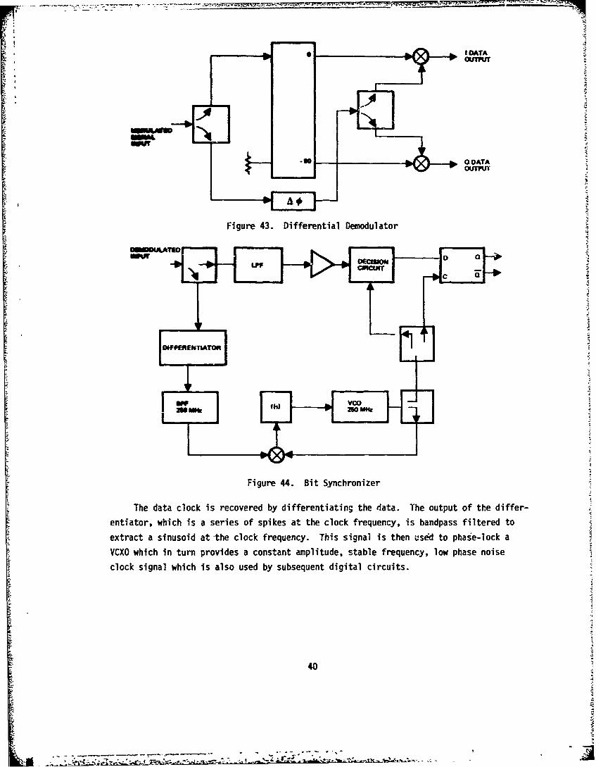
3.2.7 Differential Demodulator
The differentially encoded data is demodulated by a relatively simple technique.
The modulated input signal is split into two channels by an in-.phase power divider.
One channel is used to drive a quadrature data detector by means of a 900 hybrid and a
pair of balanced mixers. The second channel is delayed by 1 bit and is used as the
reference in the balanced mixer detectors. Therefore, the previous data bit is used
as the phase reference to demodulate the current bit. The block diagram of the
differential demodulator is shown in Figure 43.
3.2.8 Bit Synchronizer
The bit synchronizer performs two functions: clock recovery and bit decision, i.e.,
a best estimate of the digital data on a bit-by-bit basis. The bit synchronizer
accepts the output data from the demodulator, which is a composite of signal and noise,
determines the data state, and outputs this decision. A block diagram of the bit syn-I chronizer is shown in Figure 44.
S~39
[ ''
1 DATA
-V_0A OTAOUTM•"
Figure 43. Differential Demodulator
Figure 44. Bit Synchronizer
The data clock is recovered by differentiating the data. lThe output of the differ-
entiator, which is a series of spikes at the clock frequency, is bandpass filtered to
extract a sinusoid at -the clock frequency. This signal is then used to phase-lock a
VCXO which in turn provides a constant amplitude, stable frequency, low phase noise
clock signal which is also used by subsequent digital circuits.
40

3.2.9 Demultiplexer
The demultiplexer is used only when the system is configured for !SK operation.The circuit consists of two type D flip-flops which are alternately clocked at one-half the data rate. Therefore each flip-flop is set by every other data input. The
output of one of the flip-flops is inverted, which effectively inverts the state ofevery other input bit. If the two outputs are multiplexed, the original data would beregenerated. However, the Tau-Tron data detector can accept the data and delayed dataoutputs directly. The two data outputs are true PRN data sequences which are bit errorrate counted by the Tau-Tron data detector. A block diagram of the demultiplexer is
shown in Figure 45.
D DATA
D $ DELAYEDDATA
CLOCK C-2
Figure 45. Demultiplexer
41
APPENDIX
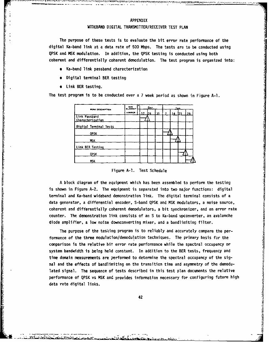
WIDEBAND DIGITAL TRANSMITTER/RECEIVER TEST PLAN
The purpose of these tests is to evaluate the bit error rate performance of the
digital Ka-band link at a data rate of 500 Mbps. The tests are to be conducted using
QPSK and MSK modulation. In addition, the QPSK testing is conducted using both
coherent and differentially coherent demodulation. The test program is organized into:
* Ka-band link passband characterization
* Digital terminal BER testing
* Link BER testing.
The test program is to be conducted over a 7 week period as shown in Figure A-l.
.uU@Ep 17 1; 4 1 •1 7 14 171 2JL
Link PassbandCharacterization
Digital Terminal Tests
Link BER TestingI
Figure A-1. Test Schedule
A block diagram of the equipment which has been assembled to perform the testing
is shown in Figure A-2. The equipment is separated into two major functions: digital
terminal and Ka-band wideband demonstration link. The digital terminal consists of a
data generator, a differential encoder, S-band QPSK and MSK modulators, a noise source,
coherent and differentially coherent demodulators, a bit synchronizer, and an error rate
counter. The demonstration link consists of an S to Ka-band upconverter, an avalanche
diode amplifier, a low noise downconverting mixer, and a bandlimiting filter.
The purpose of the tes~ing program is to reliably and accurately compare the per-
formance of the three modulation/demodulation techniques. The primary basis for the
comparison is the relative bit error rate performance while the spectral occupancy or
system bandwidth is being held constant. In addition to the BER tests, frequency and
time domain measurements are performed to determine the spectral occupancy of the sig-
nal and the effects of bandlimiting on the transition time and asymmetry of the demodu-
lated signal. The sequence of tests described in this test plan documents the relative
performance of QPSK vs MSK and provides information necessary for configuring future high
data rate digital links.
42
-Li

LC
0 >
C3C
4x
10
14.1
C3 130
cci
* &A-
CYC
S- o
coo
43@

1. LINK PASSBAND CHARACTERIZATION
Purpose: To characterize the microwave components used to assemble the Ka-band wideband
demonstration link.
Procedure: The swept phase and gain of each component (Figure A-2) are measured using
the test equipment shown in Figure A-3. The input power is varied above and below thenominal value for each component to determine the AM/AM and AM/PM conversion in eachcomponent. Table A-1 summarizes the tests performed, the data recorded, and the dataanalysis perforwd to characterize the Ka-band demonstration link. All of the measure-ments are Gaken over a 600 MHz bandwidth centered about a frequency of 2.144 GHz.
TABLE A-1. LINK PASSBAND MEASUREMENI SUMMARY
Data Recorded Measurement Range Data Reduction
Swept Swept ('J -C-
Equipment Under Test co Phase an ,• .
C-
U/C- D/C X X X X X Xxx X X X X X X X
U/C-ADA- D/C X X X X X X XX X X X X X X X
BPF X X X X X X X
U/C - ADA - D/C - BPF X X X X X X X
UIC - UPCONVERTER DIC - DOWWCONVERTER ADA - AVALANCHE DIODE AMPIUFIER BPF - BAN)FASS FILTER
Step
, Attenuator
FeIge .3.CSupler Meas Unit Under TestGenerator • 1Ts
S I-. -Ref.
ALC
NetworkAnalyzer
PenRecorder
Figure A-3. Swept Measurement Test Equipment
44

V. 4
2. DIGITAL TERMINAL TESTS
Prpose: To determine the bit error rate performance of the digital test equipment.The equipment to be tested includes the S-band QPSK and MSK modulators, the coherentand differentially coherent demodulators, and the bit synchronizer.
Procedure: The equipment under test is configured as shown in Figure A-4. Themodulator/demodulator configurations to be evaluated are:
Modulator Demodulator
QPSK CoherentQPSK Differentially coherentMSK Coherent
The modulated (QPSK or MSK) S-band signal is directly demodulated. The only postmodulation distortion introduced is due to the S-band amplifier following the modulator.The results of.these tests indicate the BER performance of the digital terminal alone.
Data Bit ErrorGenerator Synchrnjzer Counter
QPSK Noise CoherentQ Modulator Source D od atr
ifferentia QPSK Noise iffernaQ._ Ecoetor••l Coherent•Encoder Modul~ator Source
SK Noise CherntModulator Source Demodulator
Figure A-4. Digital Terminal Test Configuration
The BER performance of the digital equipment is characterized for error probabili-ties of >10' to <10 . Broadband thermal noise is added to the modulated S-band signaljust before the demodulator to simulate the required Eb/No range.
The BER of the equipment under test is determined by averaging the error rates ofthe I and Q channel. A sample data sheet is shown in Figure A-5, and the data isplotted on the form shown in Figure A-6. Several measurements over a period of severaldays are performed and the results averaged. This is done to eliminate any anomalous
45
:'z~ . • •,•: .• - •- •~. " - " "'• .

data points. Using this technique, we have est,'ilished a measurement repeatability ofbetter than ±0.3 dB for an error probability of 10- 6 .
Configuration
Date
L.P.F.
Eb Error CountE-
No I Channel Q Channel Average
Figure A-5. Example Error Count Data Sheet
In addition to the BER data, time and frequency domain photographs are taken ofthe baseband, modulated, and demodulated signals as indicated in Table A-2. The photo-graphs are analyzed to determine the transition time, asymmetry, and the spectrumoccupancy of the signal.
3. LINK BIT ERROR RATE TESTING
Purpose: To determine the degration in digital terminal BER due to the distortion inthe Ka-band wideband demonstration link.
Procedure: The basic procedure is to repeat all of the tests described in Section 2.The only difference is that the modulated signal is transmitted through the demonstra-tion link prior to being demodulated. In this way, the input and output data can be ,compared to determine the effects of the demonstration link for such factors as BER,risetime, asymmetry, and spectrum occupancy. •
; 46
_________A

1-4
i I q Iii
lu
litITT I
10-60
Figure ~ ~ ~ ~ ~ :11 A-6 Eape i ro Rt uv
1P I mi 47
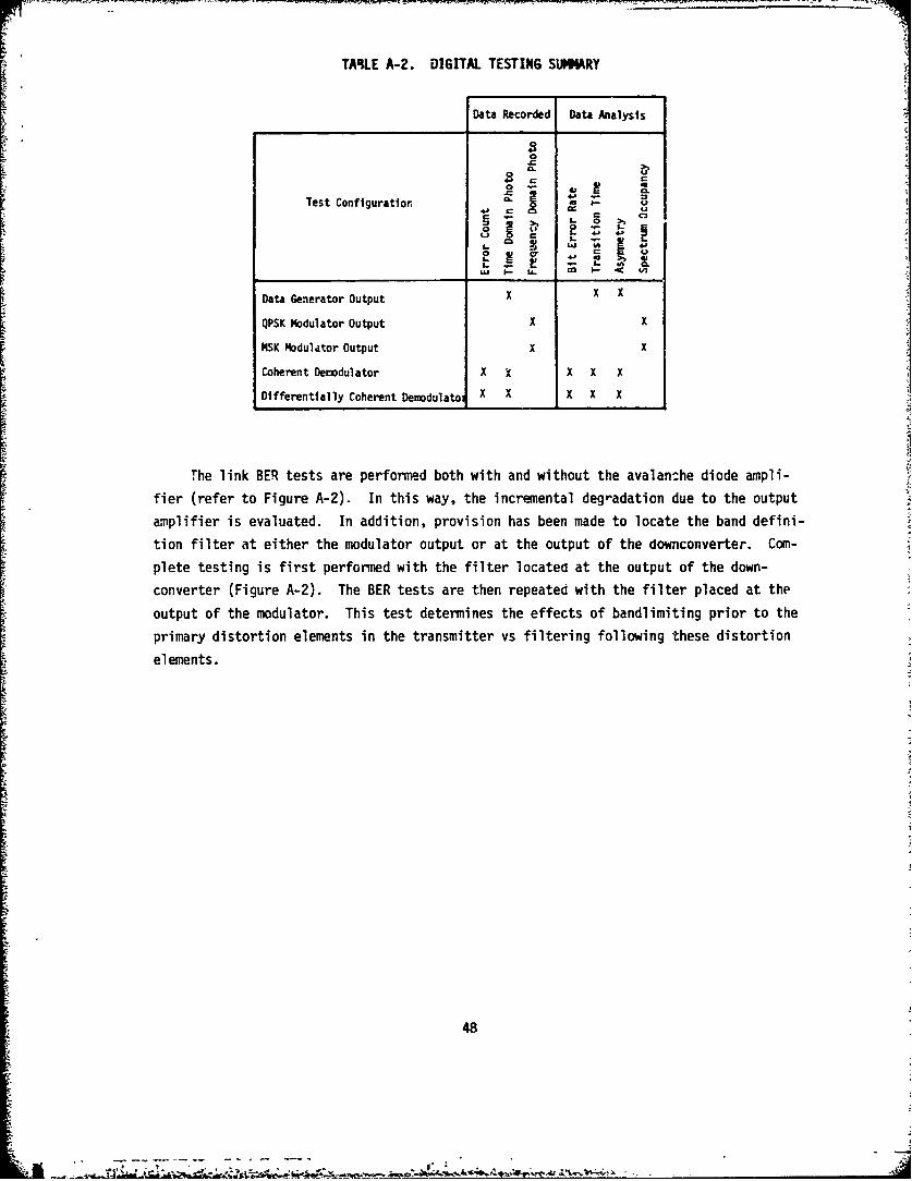
TALE A-2. DIGITAL TESTING SUMMARY
Data Recorded Data Analysis
0
0
0
D Ta enertConfigurtion L 0
C1.0 0
Cs =-0
QPSK M4odulator Output xX
M4SK M~odula'tor Output xX
Coherent Confdurator X X X X X
Differentilaly Coherent Demodulatoi X X X X X
The link BER tests are performe~d both with and without the avalans.he diode ampli-
fier (refer to Figure A-2). In this way, the incremental degradation due to the output
amplifier is evaluated. In addition, provision has been made to locate the band defini-
tion filter at either the modulator output or at the output of the downconverter. Com-
plete testing is first performed with the filter locatea at the output of the down-
converter (Figure A-2). The BER tests are then repeated with the filter placed at the
output of the modulator. This test determines the effects of bandlimiting prior to the
primary distortion elements in the transmitter vs filtering following these distortion
elements.
48

-•." - . ....~ - ...... - .... "-. /
Rome Air Development Center
RAW plans and conducts research, exploratory and advanceddeveloxrient programs in command, control, and comranicatlons(C) activities, and in the C3 areas of information sciencesand intelligence. The principal technical mission areasare communications, electromagnetic guidance and control,surveillance of ground and aerospace objects, intelligencedata collection and handling, information system technology,Ionospheric propagation, solid state sciences, microwavephysics and electronic reliability, maintainability andcompatibility.
SI,•",6 . 9ib.4%.T14
',.,I • '0