search.jsp?R=19940011473 2018-10-29T23:41:37+00:00Z N94 ... · GSC 13,541-1 2 NOTICE The invention...
24
(NASA-Caso-GSC-13541-1) i]nU_LE-DRIVEN SHIELD CAPACITIVE TYPF PROXIMITY SENSQR Patent App] ic:ition (_ASA) 24 p N94-I5946 Unclas - / G3/63 0190831 NASA CASE NO. PRINT FIG. GSC 13,541-I 2 NOTICE The invention disclosed in this document resulted from research in aeronautical and space activities performed under programs of the National Aeronautics and Space Administration. The invention is owned by NASA and is, therefore, available for licensing in accordance with the NASA Patent Licensing Regulation (14 Code of Federal Regulations 1245.2). To encourage commercial utilization of NASA-owned inventions, it is NASA policy to grant licenses to commercial concerns. Although NASA encourages nonexclusive licensing to promote competition and achieve the widest possible utilization, NASA will consider the granting of a limited exclusive license, pursuant to the NASA Patent Licensing Regulations, when such a license will provide the necessary incentive to the _ licensee to achieve early practical application of the invention Address inquiries and all applications for license for this invention to NASA Patent Counsel GoddardSpaceFlight Center Code 204 Greenbelt, MD 20771 Approved NASA forms for application for nonexclusive or exclusive license are available from the above address. Serial No.: Filing Dale: 08/008,426 1/25/93 GSSI_ https://ntrs.nasa.gov/search.jsp?R=19940011473 2018-11-12T09:24:50+00:00Z
Transcript of search.jsp?R=19940011473 2018-10-29T23:41:37+00:00Z N94 ... · GSC 13,541-1 2 NOTICE The invention...

(NASA-Caso-GSC-13541-1)
i]nU_LE-DRIVEN SHIELD CAPACITIVE
TYPF PROXIMITY SENSQR Patent
App] ic:ition (_ASA) 24 p
N94-I5946
Unclas - /
G3/63 0190831
NASA CASE NO.
PRINT FIG.
GSC 13,541-I
2
NOTICE
The invention disclosed in this document resulted from research in
aeronautical and space activities performed under programs of the
National Aeronautics and Space Administration. The invention is
owned by NASA and is, therefore, available for licensing in
accordance with the NASA Patent Licensing Regulation (14 Code of
Federal Regulations 1245.2).
To encourage commercial utilization of NASA-owned inventions, it
is NASA policy to grant licenses to commercial concerns. Although
NASA encourages nonexclusive licensing to promote competition and
achieve the widest possible utilization, NASA will consider the
granting of a limited exclusive license, pursuant to the NASA
Patent Licensing Regulations, when such a license will provide the
necessary incentive to the _ licensee to achieve early practical
application of the invention
Address inquiries and all applications for license for this
invention to NASA Patent Counsel GoddardSpaceFlight Center Code 204
Greenbelt, MD 20771
Approved NASA forms for application for nonexclusive or exclusive
license are available from the above address.
Serial No.:
Filing Dale:08/008,426
1/25/93 GSSI_
https://ntrs.nasa.gov/search.jsp?R=19940011473 2018-11-12T09:24:50+00:00Z
NSA GSCI3, 541-1
AWARDS DIGEST
DOUBLE-DRIVEN SHIELD CAPACITIVE TYPE PROXIMITY SENSOR
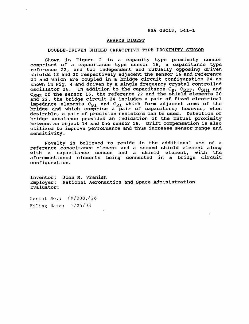
Shown in Figure 2 is a capacity type proximity sensor
comprised of a capacitance type sensor 16, a capacitance type
reference 22, and two independent and mutually opposing driven
shields 18 and 20 respectively adjacent the sensor 16 and reference
22 and which are coupled in a bridge circuit configuration 24 as
shown in Fig. 4 and driven by a single frequency crystal controlled
oscillator 26. In addition to the capacitance Cs, CREF, CSH 1 and
CSH 2 of the sensor 16, the reference 22 and the shield elements 20
and 22, the bridge circuit 24 includes a pair of fixed electrical
impedance elements CSI and CRI which form adjacent arms of the
bridge and which comprise a pair of capacitors; however, when
desirable, a pair of precision resistors can be used. Detection of
bridge unbalance provides an indication of the mutual proximity
between an object 14 and the sensor 16. Drift compensation is also
utilized to improve performance and thus increase sensor range and
sensitivity.
Novelty is believed to reside in the additional use of a
reference capacitance element and a second shield element along
with a capacitance sensor and a shield element, with the
aforementioned elements being connected in a bridge circuit
configuration.
Inventor:
Employer:Evaluator:
John M. Vranish
National Aeronautics and Space Administration
_;erial No.: 08/008,426
Filing Date: 1/25/93

NASA CASE NO.
PRINT FIG.
GSC 13,541-1
2
NOTICE
The invention disclosed in this document resulted from research in
aeronautical and space activities performed under programs of the
National Aeronautics and Space Administration. The invention is
owned by NASA and is, therefore, available for licensing in
accordance with the NASA Patent Licensing Regulation (14 Code of
Federal Regulations 1245.2).
To encourage commercial utilization of NASA-owned inventions, it
is NASA policy to grant licenses to commercial concerns. Although
NASA encourages nonexclusive licensing to promote competition and
achieve the widest possible utilization, NASA will consider the
granting of a limited exclusive license, pursuant to the NASA
Patent Licensing Regulations, when such a license will provide the
necessary incentive to the _ licensee to achieve early practical
application of the invention
Address inquiries and all applications for license for this
invention to NASA Patent Counsel Goddard Space Flight Center Code 204
Greenbelt, MD 20771
Approved NASA forms for application for nonexclusive or exclusive
license are available from the above address.
Serial No.:
Filing Dale:08/008,426
1/25/93 GSFI7
Serial No.: 08/008,426Filing Date: 1/25/93
NASA GSC13,541-I
DOUBLE-DRIVEN SHIELD CAPACITIVE TYPE PROXIMITY SENSOR
5
i0
15
2O
Oriqin of the Invention
This invention was made by an employee of the United
States Government and accordingly may be manufactured and
used by or for the Government for governmental purposes
without the payment of any royalties thereon or therefor.
Backqround of the Invention
Field of the Invention
The present invention relates generally to
capacitive type proximity sensors and more particularly
to a capacitive type "capaciflector" proximity sensor
which includes a driven shield element behind the sensor.
Description of the Prior Art
Capacitive sensors used for proximity sensing and
collision avoidance are generally known. However, such
sensors do not adequately control stray capacitance and
consequently do not perform with an adequate range and
sensitivity for many applications such as docking and
berthing in outer space.
In U.S. Patent 5,166,679, entitled "Driven Shielding
Capacitive Proximity Sensor", John M. Vranish, which
issued November 24, 1992, the teachings of which are
incorporated herein by reference, there is disclosed a
capacitive sensing element which uses a capacitively
controlled oscillator to drive the sensor element as well
as a voltage follower driven shield member located behind

- 2 - GSC13,541-I
i0
15
2O
25
the sensor element to reflect energy toward an intruding
object to substantially increase range and sensitivity.
The intruding object forms an additional capacitive path
to ground which in turn alters the frequency of the
oscillator. This frequency change is converted to a DC
output signal by a frequency to voltage converter.
Such a proximity sensor, however, includes several
inherent limitations which include, for example: the
central frequency of the oscillator tends to drift as a
function of changes in temperature and humidity; the
frequency to voltage converter is relatively large in
size and consumes a substantial amount of power; and the
components and their connections as well as the
arrangements in front of a relatively high gain output
amplifier presents a source of low frequency drift, and
since the signal output is in the low frequency region,
this has a tendency to reduce sensor range and
sensitivity.
Summary
It is an object of the present invention, therefore,
to provide an improvement in capacitive type proximity
sensors.
It is a further object of the invention to provide
an improvement in capacitive type proximity sensors which
include a driven shielding member.

- 3 - GSC13,541-I
5
i0
15
2O
25
It is still another object of the invention to
provide a proximity sensor which will sense the proximity
of humans or unexpected structures at a range sufficient
to provide collision avoidance such as during docking and
berthing operations in outer space.
It is yet another object of the invention to provide
a proximity sensor which can be used to determine the
location of pins, holes and edges in equipment with
sufficient accuracy to permit alignment prior to docking
and berthing.
And it is still yet another object of the invention
to provide an improvement in proximity sensors which will
permit machines and/or astronauts to guide payloads
precisely into latching devices and to anticipate touch-
down just prior before it occurs so as to permit a very
soft mating process during
procedure in outer space.
Briefly, the foregoing
a docking and berthing
and other objects are
achieved by a capacity type proximity sensor comprised of
a capacitance type sensor, a capacitance type reference,
and two independent and mutually opposing driven shields
respectively adjacent the sensor and reference and which
are coupled in a bridge circuit configuration and driven
by a single frequency crystal controlled oscillator. The
bridge circuit additionally includes a pair of fixed

- 4 - GSC13,541-I
5
i0
15
20
25
electrical impedance elements which form adjacent arms of
the bridge and which comprise either a pair of precision
resistances or capacitors. Detection of bridge unbalance
provides an indication of the mutual proximity between an
object and the sensor. Drift compensation is also
utilized to improve performance and thus increase sensor
range and sensitivity.
Brief Description of the Drawinqs
The following detailed description of the invention
will be more readily understood when considered together
with the accompanying drawings in which:
Figure 1 is a diagram illustrating the electric
field distribution of a capacitance type proximity sensor
in accordance with the known prior art;
Figure 2 is a diagram illustrative of the electrical
field distribution of a proximity sensor in accordance
with the present invention;
Figures 3A-3D depict a set of equivalent circuits
for the capacitance elements shown in Figure 2;
Figure 4 is an electrical schematic diagram
illustrative of the elements shown in Figure 2 connected
in a bridge configuration;
Figure 5 is an electrical schematic diagram
depicting a first preferred embodiment of the subject
invention;

- 5 - GSC13,541-I
i0
15
2O
25
Figure 6 is an electrical schematic diagram
illustrative of a second preferred embodiment of the
invention;
Figure 7 is an electrical schematic diagram
illustrative of a third preferred embodiment of the
invention; and
Figure 8 is an electrical schematic diagram
illustrative of a fourth preferred embodiment of the
subject invention.
Detailed Description of the Invention
Referring now to the drawings and more particularly
to Figure i, shown thereat is an electrical field
distribution system of a driven shield capacitance type
sensor, also referred to as a "capaciflector" sensor
which is shown and described in detail in above
referenced U.S. Patent No. 5,166,679. In such a sensor
system, a piece of apparatus 12 which may be, for
example, the skin of a robotic arm and which is to be
protected from the presence and position of an intruding
object 14, includes a sensor element 16 which comprises
a thin sheet of conductive material which is driven by an
electronic circuit, not shown, and which acts as one
electrode of a capacitor, the second electrode of which
is provided by the intruding object 14. The capacitor
thus formed controls the frequency of an oscillator, also

- 6 - GSC13,541-I
I0
15
2O
25
not shown, which operates so that when an object for some
reason or another intrudes, the output frequency of the
oscillator changes. The grounded objects in the vicinity
of the conductor sheet 16 and the lead wires between the
circuit and the sheet 16 create a large fixed parasitic
capacitance which reduces sensor sensitivity to the
intruding object 14.
To increase the sensitivity of the capacitance type
proximity sensor by reducing the parasitic capacitance
exhibited by the electric field shown in Figure i, the
prior art system shown and described in U.S. Patent No.
5,166,679 provides for the insertion of a second
relatively thin sheet 18 of conductive material which is
substantially wider than the sensor 16 and is located
between the sensor 16 and the apparatus being protected
12. This generates an electric field distribution such
that the member 18 acts as a shield for the capacitive
sensor 16 where the field concentration is centered
between it and the object 14, with a substantially
smaller field returning directly to the grounded
apparatus 12.
The shield member 18, furthermore, is driven at the
same instantaneous voltage as the capacitor sensor 16,
however, it is not frequency sensitive to nearby objects
as is the sensor 16. Thus the sensor 16 is shielded from
- 7 - GSC13,541-I
5
i0
15
2O
25
nearby ground, i.e. the apparatus 12, such that the
capacitance between it and the arm is substantially
reduced.
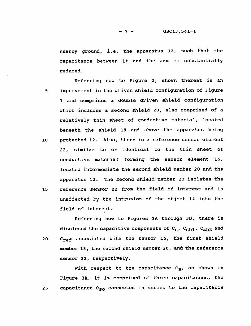
Referring now to Figure 2, shown thereat is an
improvement in the driven shield configuration of Figure
1 and comprises a double driven shield configuration
which includes a second shield 20, also comprised of a
relatively thin sheet of conductive material, located
beneath the shield 18 and above the apparatus being
protected 12. Also, there is a reference sensor element
22, similar to or identical to the thin sheet of
conductive material forming the sensor element 16,
located intermediate the second shield member 20 and the
apparatus 12. The second shield member 20 isolates the
reference sensor 22 from the field of interest and is
unaffected by the intrusion of the object 14 into the
field of interest.
Referring now to Figures 3A through 3D, there is
disclosed the capacitive components of Cs, Cshl, Csh 2 and
Cre f associated with the sensor 16, the first shield
member 18, the second shield member 20, and the reference
sensor 22, respectively.
With respect to the capacitance Cs, as shown in
Figure 3A, it is comprised of three capacitances, the
capacitance Cso connected in series to the capacitance

- 8 - GSC13,541-I
5
i0
15
2O
Cog which is shunted by the capacitance Csg, where Cso is
the capacitance between the sensor 16 and the object 14,
Cog is the capacitance of the object 14 to ground and Csg
is the capacitance between the sensor 16 and ground. As
shown in Figure 3B, the capacitance Csh I associated with
the shield 18 is comprised of the series combination of
Cshlo and Cog shunted by capacitance Cshlg and C'ref,
where Cshlo comprises the capacitance between the shield
18 and the object 14, Cog comprises a capacitance between
the object 14 and ground, Cshlg is the capacitance of the
shield 18 to ground and C're f is a negative capacitance
indicative of a current source for a bridge circuit
arrangement shown in Figures 4-8, to be described. The
second shield capacitance Csh2, as shown in Figure 3C, is
the combination of four capacitances, the first being
Csh2g which is shunted by a series combination of
Cshlsh2, and Cshlo with the latter being further shunted
by the capacitance Cshlg ' where Csh2g comprises the
capacitance between the second shield 20 and ground,
Cshlsh2 comprises the capacitance between the two shields
18 and 20, Cshlo comprises the capacitance between the
first shield 18 and the object 14 and Cshlg comprises the
capacitance between the first shield 18 and ground.
Finally, Cre f comprises a single capacitance as shown in

- 9 - GSC13,541-I
5
I0
15
2O
25
Figure 3D and comprises the capacitance between the
reference element 22 and ground.
As shown in Figure 4, the four elements 16, 18, 20
and 22 represented by their capacitances are connected in
adjacent arms of a bridge circuit 24 which also includes
a pair of fixed impedances represented by capacitances
Csl and Crl in opposing adjacent arms. The bridge
circuit is shown being energized by a single signal
source 26 which comprises a crystal controlled
oscillator. The crystal controlled oscillator 26 outputs
a highly stable single frequency signal. Following
bridge balance, intrusion by the object 14 into a region
of interest in the vicinity of the sensor 16 forces the
bridge 24 out of balance.
As illustrated in Figure 5, there the bridge circuit
24 is redrawn in order to further disclose the inclusion
of a pair of operational amplifiers configured to operate
as high input impedance/low output impedance voltage
follower circuits 28 and 30, which are coupled to the
crystal controlled oscillator 26 through the capacitances
Csl and Crl to drive the shields 18 and 20 (Figure 2)
forming the capacitances Csh I and Csh 2. Bridge balance
is detected by means of a differential amplifier 32
coupled across the bridge circuit nodes 34 and 36 and
where circuit node 38 common to the resistances Csl and
- i0 - GSC13,541-I
5
i0
15
2O
25
Crl are connected to one side of the crystal oscillator
26, with circuit node 40 being connected to ground along
with the opposite side of the crystal oscillator 26.
The differential amplifier 32 provides a voltage signal
output Vsig at terminal 42.
In accordance with classic voltage divider bridge
detection circuits, if the impedances of the capacitances
C s and Cre f are equal as well as the capacitive
impedances of Csl and Crl, then Vsig = 0. As the sensor
element 16 shown in Figure 2 approaches an object 14, or
vice versa, C s increases and with it the current across
Csl. This unbalances the bridge and increases Vsig. The
closer the object 14 comes to the sensor 16, the larger
Vsig becomes.
Further as shown in Figure 5, an operational
amplifier 46 having one input grounded is coupled to the
circuit node 36 and provides a reference voltage output
of KVre f at terminal 48, where K is the amplification
factor of amplifier 46. Because amplifier 46 is
connected to the other side of the bridge 24, movement of
the object 14 relative to the sensor 16 Vre f is not
affected. Upsetting the balance in the bridge means that
KVre f > Vsig. This, in turn, results in current leakage
from the reflective shield 20 behind the reference
element 22 to the reflective shield 18 behind the sensor
- Ii - GSC13,541-I
i0
15
2O
25
element 16. However, the shield 20 behind the reference
sensor 22 is slaved to the reference capacitance Cre f by
the voltage follower 30. The shield capacitance Csh I is
similarly slaved to the capacitance of the sensing
element C s via the voltage follower circuit 28. Thus any
leakage current cannot affect either Vre f or Vsig, thus
enhancing performance.
It is to be noted that KVre f is precisely defined
throughout all operations. Ground is made an integral
part of the structure by virtue of the apparatus 12 being
grounded and is precisely located with respect to the
capacitance Cre f and its reflecting shield capacitance
Csh 2 . The second shield element 20 isolates the
reference element 22 from the effects of the object 14
and the sensor 16 and thus KVre f is clearly defined no
matter how the system is mounted and no matter what is
occurring with respect to the relative position of the
sensor 16 and the object 14.
The circuit elements are specifically designed to
compensate for any changing environment, such as by
selecting precision capacitors with like characteristics
for the capacitances Csl and Crl and being located next
to one another so that they are subject to the same
variations in temperature. The amplifiers 28, 30, 32 and
46 are also co-located on a common printed circuit board

- 12 - GSC13,541-I
5
I0
15
2O
and become part of a common structure which is equally
affected by the changing environment.
It is also to be noted that the circuitry shown in
Figure 5 also provides a technique for drift measurement
and is accomplished by locating the output amplifier 32
adjacent the amplifier 46. Since the main source of
drift would be temperature induced variations in the
components, the gain K of amplifier 46 is measured at the
start of an operation and is given a value KO. Since
Cre f and Crl changes relatively little during operation,
particularly if the reference currents are kept low, any
observed variation in the output of KVre f will be caused
by a variation of gain K in the high gain amplifier and
thus provide a measure of drift.
While the circuitry shown in Figures 4 and 5
disclose the concept of a simple differential amplifier
32 for detecting any change in the bridge circuit 24, the
concept of peak detection can also be utilized when
desirable, and comprises a preferred method of detection.
This method merely requires the addition of a pair of
peak detectors to the bridge output terminals.
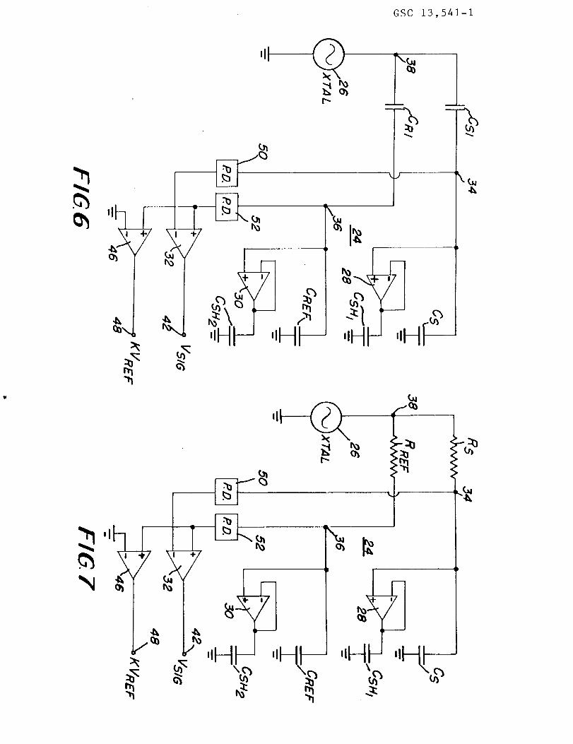
Accordingly, a pair of peak detector circuits 50 and 52,
as shown in Figure 6, are coupled to the bridge circuit
nodes 34 and 36, with the output to the peak detectors 50

- 13 - GSC13,541-I
I0
15
2O
25
and 52 then being fed to the two inputs of the
differential amplifier 32 as before.
Referring now to Figure 7 where there is shown
another preferred embodiment of
addition to the peak detectors 50
capacitors in adjacent arms of
the invention, in
and 52, the fixed
the bridge 24 and
comprising the capacitances Csl and Crl are replaced by
precision resistors having fixed resistance values Rs and
Rref, respectively. The trade off would be determined by
the relative temperature characteristics of the
capacitive components as opposed to resistive components
in adjacent arms of the bridge, including the shielding
elements and the sensor elements shown in Figure 2.
Also, phase discrimination can be used in place of
peak detection, for example, as shown in the embodiment
of Figure 8, where a phase comparator 54 is utilized in
place of the peak detectors 50 and 52, shown in Figure 6.
When desirable, the same substitution can be used for the
embodiment shown in Figure 6.
With respect to the selection of the capacitors or
resistors for adjacent arms of the bridge 24 providing
the impedances Rref, Rs and Csl, Crl, respectively, the
fixed resistor arrangement shown in Figures 6 and 7
provide a bridge circuit which acts as a simple voltage
divider, with both the left and right sides of the bridge
- 14 - GSC13,541-I
5
i0
15
2O
25
being in phase no matter how large or how small the
output signal. The capacitors can be built into the
printed circuit board and thus make the sensor extremely
compact with each component being mutually referenced
with respect to the other.
Since a single frequency is utilized, frequency
stabilized crystal controlled oscillators can be employed
and became desirable because frequency drift over long
periods of time is substantially reduced, thus permitting
indefinite operation in space. This also permits narrow
band filtering where required, which improves signal to
noise and thus range and sensitivity.
The circuitry employed in the present invention
becomes relatively simple inasmuch as the frequency to
voltage conversion apparatus which consumes far too much
power and typically utilized in the prior art is
eliminated. In addition to eliminating the frequency to
voltage converters, only a few elements are utilized and
these comprise peak detectors, resistors and operational
amplifiers which are relatively simple and compact.
Capacitors, moreover, can be built into the printed
circuit board and so are also extremely compact. Since
all the components can be built into the same circuit
board structure, these elements can be precisely located
with respect to one another, thus drastically reducing
- 15 - GSC13,541-I
i0
parasitic capacitances and losses, while those that do
remain are repeatable and predictable. Furthermore,
drift minimization and control are easily implemented.
Having thus shown and described what is at present
considered to be the preferred embodiment of the
invention, it should be noted that the same has been made
by way of illustration and not limitation. Accordingly,
all modifications, alterations and changes coming within
the spirit and scope of the invention are herein meant to
be included.

/6GSC13,541-I
5
I0
15
ABSTRACT
A capacity type proximity sensor comprised of a
capacitance type sensor, a capacitance type reference,
and two independent and mutually opposing driven shields
respectively adjacent the sensor and reference and which
are coupled in an electrical bridge circuit configuration
and driven by a single frequency crystal controlled
oscillator. The bridge circuit additionally includes a
pair of fixed electrical impedance elements which form
adjacent arms of the bridge and which comprise either a
pair of precision resistances or capacitors. Detection
of bridge unbalance provides an indication of the mutual
proximity between an object and the sensor. Drift
compensation is also utilized to improve performance and
thus increase sensor range and sensitivity.

' GSC 13,541-I
14
1(9
[12
FIGIPRIOR ART
• t
i
14
_/Cs
CREF /2
FIC 2

GSC 13,541-1
\
m
m
m
w
L_7_m
Y
FIG. JA
k...
___zCsHI _ _
= - f_,,,g=/Cog--
V
FI6.3B
J
\
I
iCsH2 g _L,"CsH_sH2
I TA_ _5_c_,,,g
Y.2
FIG. 3C
gI
._C REF g
T
\ J

GSC 13,541-i
26
_X TA L
3_
._z
FIG 4
38\
26
XTAL
FIG5
38
]I32
28
m
.j__/CsH2
m
VS/G42
KVREF
GSC 13,541-1
,tl
,,HJ K'

GSC 13,541-I
XTA L
RREF
36
m
[ COMP.
34J
-._1_e_ T
CSHI
---- CREF
_m
./_ - CSH230 --
im
42
FIG. 8


![II N94-33493 - NASA · ii n94-33493 high performance jet-engine flight ... w nch instruments & transmitter] ... 1171. flight ensemble averaging](https://static.fdocuments.us/doc/165x107/5bc3cd6509d3f299608d70f1/ii-n94-33493-nasa-ii-n94-33493-high-performance-jet-engine-flight-w-nch.jpg)