R Platform Flash In-System Programmable Configuration PROMS · PDF filePlatform Flash...
42
DS123 (v2.7) July 11, 2005 www.xilinx.com 1 Product Specification © 2005 Xilinx, Inc. All rights reserved. All Xilinx trademarks, registered trademarks, patents, and disclaimers are as listed at http://www.xilinx.com/legal.htm . All other trademarks and registered trademarks are the property of their respective owners. All specifications are subject to change without notice. Features • In-System Programmable PROMs for Configuration of Xilinx FPGAs • Low-Power Advanced CMOS NOR FLASH Process • Endurance of 20,000 Program/Erase Cycles • Operation over Full Industrial Temperature Range (–40°C to +85°C) • IEEE Standard 1149.1/1532 Boundary-Scan (JTAG) Support for Programming, Prototyping, and Testing • JTAG Command Initiation of Standard FPGA Configuration • Cascadable for Storing Longer or Multiple Bitstreams • Dedicated Boundary-Scan (JTAG) I/O Power Supply (V CCJ ) • I/O Pins Compatible with Voltage Levels Ranging From 1.5V to 3.3V • Design Support Using the Xilinx Alliance ISE and Foundation ISE Series Software Packages • XCF01S/XCF02S/XCF04S - 3.3V supply voltage - Serial FPGA configuration interface (up to 33 MHz) - Available in small-footprint VO20 and VOG20 packages. • XCF08P/XCF16P/XCF32P - 1.8V supply voltage - Serial or parallel FPGA configuration interface (up to 33 MHz) - Available in small-footprint VO48, VOG48, FS48, and FSG48 packages - Design revision technology enables storing and accessing multiple design revisions for configuration - Built-in data decompressor compatible with Xilinx advanced compression technology Description Xilinx introduces the Platform Flash series of in-system pro- grammable configuration PROMs. Available in 1 to 32 Megabit (Mbit) densities, these PROMs provide an easy-to-use, cost-effective, and reprogrammable method for storing large Xilinx FPGA configuration bitstreams. The Platform Flash PROM series includes both the 3.3V XCFxxS PROM and the 1.8V XCFxxP PROM. The XCFxxS version includes 4-Mbit, 2-Mbit, and 1-Mbit PROMs that support Master Serial and Slave Serial FPGA configuration modes (Figure 1). The XCFxxP version includes 32-Mbit, 16-Mbit, and 8-Mbit PROMs that support Master Serial, Slave Serial, Master SelectMAP, and Slave SelectMAP FPGA configuration modes (Figure 2). A summary of the Platform Flash PROM family members and supported fea- tures is shown in Table 1. 4 2 Platform Flash In-System Programmable Configuration PROMS DS123 (v2.7) July 11, 2005 0 Product Specification R Table 1: Platform Flash PROM Features Density V CCINT V CCO Range V CCJ Range Packages JTAG ISP Programming Serial Config. Parallel Config. Design Revisioning Compression XCF01S 1 Mbit 3.3V 1.8V - 3.3V 2.5V - 3.3V VO20/VOG20 √ √ XCF02S 2 Mbit 3.3V 1.8V - 3.3V 2.5V - 3.3V VO20/VOG20 √ √ XCF04S 4 Mbit 3.3V 1.8V - 3.3V 2.5V - 3.3V VO20/VOG20 √ √ XCF08P 8 Mbit 1.8V 1.5V - 3.3V 2.5V - 3.3V VO48/VOG48 FS48/FSG48 √ √ √ √ √ XCF16P 16 Mbit 1.8V 1.5V - 3.3V 2.5V - 3.3V VO48/VOG48 FS48/FSG48 √ √ √ √ √ XCF32P 32 Mbit 1.8V 1.5V - 3.3V 2.5V - 3.3V VO48/VOG48 FS48/FSG48 √ √ √ √ √
Transcript of R Platform Flash In-System Programmable Configuration PROMS · PDF filePlatform Flash...
DS123 (v27) July 11 2005 wwwxilinxcom 1Product Specification
copy 2005 Xilinx Inc All rights reserved All Xilinx trademarks registered trademarks patents and disclaimers are as listed at httpwwwxilinxcomlegalhtm All other trademarks and registered trademarks are the property of their respective owners All specifications are subject to change without notice
Featuresbull In-System Programmable PROMs for Configuration of
Xilinx FPGAsbull Low-Power Advanced CMOS NOR FLASH Processbull Endurance of 20000 ProgramErase Cyclesbull Operation over Full Industrial Temperature Range
(ndash40degC to +85degC)bull IEEE Standard 114911532 Boundary-Scan (JTAG)
Support for Programming Prototyping and Testingbull JTAG Command Initiation of Standard FPGA
Configurationbull Cascadable for Storing Longer or Multiple Bitstreamsbull Dedicated Boundary-Scan (JTAG) IO Power Supply
(VCCJ)
bull IO Pins Compatible with Voltage Levels Ranging From 15V to 33V
bull Design Support Using the Xilinx Alliance ISE and Foundation ISE Series Software Packages
bull XCF01SXCF02SXCF04S- 33V supply voltage- Serial FPGA configuration interface (up to 33 MHz)- Available in small-footprint VO20 and VOG20
packagesbull XCF08PXCF16PXCF32P
- 18V supply voltage- Serial or parallel FPGA configuration interface
(up to 33 MHz)- Available in small-footprint VO48 VOG48 FS48
and FSG48 packages- Design revision technology enables storing and
accessing multiple design revisions for configuration
- Built-in data decompressor compatible with Xilinx advanced compression technology
DescriptionXilinx introduces the Platform Flash series of in-system pro-grammable configuration PROMs Available in 1 to 32Megabit (Mbit) densities these PROMs provide aneasy-to-use cost-effective and reprogrammable methodfor storing large Xilinx FPGA configuration bitstreams ThePlatform Flash PROM series includes both the 33VXCFxxS PROM and the 18V XCFxxP PROM The XCFxxSversion includes 4-Mbit 2-Mbit and 1-Mbit PROMs that
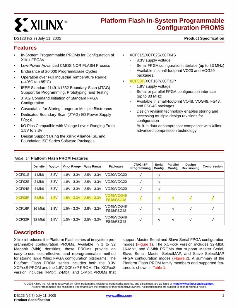
support Master Serial and Slave Serial FPGA configurationmodes (Figure 1) The XCFxxP version includes 32-Mbit16-Mbit and 8-Mbit PROMs that support Master SerialSlave Serial Master SelectMAP and Slave SelectMAPFPGA configuration modes (Figure 2) A summary of thePlatform Flash PROM family members and supported fea-tures is shown in Table 1
42 Platform Flash In-System Programmable
Configuration PROMSDS123 (v27) July 11 2005 0 Product Specification
R
Table 1 Platform Flash PROM Features
Density VCCINT VCCO Range VCCJ Range Packages JTAG ISP Programming
Serial Config
Parallel Config
Design Revisioning Compression
XCF01S 1 Mbit 33V 18V - 33V 25V - 33V VO20VOG20 radic radic
XCF02S 2 Mbit 33V 18V - 33V 25V - 33V VO20VOG20 radic radic
XCF04S 4 Mbit 33V 18V - 33V 25V - 33V VO20VOG20 radic radic
XCF08P 8 Mbit 18V 15V - 33V 25V - 33V VO48VOG48FS48FSG48 radic radic radic radic radic
XCF16P 16 Mbit 18V 15V - 33V 25V - 33V VO48VOG48FS48FSG48 radic radic radic radic radic
XCF32P 32 Mbit 18V 15V - 33V 25V - 33V VO48VOG48FS48FSG48 radic radic radic radic radic
huffman
XCF08P 8 Mbit 18V 15V - 33V 25V - 33V VO48VOG4813FS48FSG48 radic radic radic radic radic
huffman
XCF08P
Platform Flash In-System Programmable Configuration PROMS
DS123 (v27) July 11 2005 wwwxilinxcom 2Product Specification
R
When the FPGA is in Master Serial mode it generates aconfiguration clock that drives the PROM With CF High ashort access time after CE and OE are enabled data isavailable on the PROM DATA (D0) pin that is connected tothe FPGA DIN pin New data is available a short accesstime after each rising clock edge The FPGA generates theappropriate number of clock pulses to complete the config-uration When the FPGA is in Slave Serial mode the PROM and theFPGA are both clocked by an external clock source oroptionally for the XCFxxP PROM only the PROM can beused to drive the FPGArsquos configuration clockThe XCFxxP version of the Platform Flash PROM also sup-ports Master SelectMAP and Slave SelectMAP (or SlaveParallel) FPGA configuration modes When the FPGA is inMaster SelectMAP mode the FPGA generates a configura-tion clock that drives the PROM When the FPGA is in SlaveSelectMAP Mode either an external oscillator generatesthe configuration clock that drives the PROM and theFPGA or optionally the XCFxxP PROM can be used todrive the FPGArsquos configuration clock With BUSY Low and
CF High after CE and OE are enabled data is available onthe PROMs DATA (D0-D7) pins New data is available ashort access time after each rising clock edge The data isclocked into the FPGA on the following rising edge of theCCLK A free-running oscillator can be used in the SlaveParallel Slave SelecMAP modeThe XCFxxP version of the Platform Flash PROM providesadditional advanced features A built-in data decompressorsupports utilizing compressed PROM files and design revi-sioning allows multiple design revisions to be stored on asingle PROM or stored across several PROMs For designrevisioning external pins or internal control bits are used toselect the active design revisionMultiple Platform Flash PROM devices can be cascaded tosupport the larger configuration files required when target-ing larger FPGA devices or targeting multiple FPGAs daisychained together When utilizing the advanced features forthe XCFxxP Platform Flash PROM such as design revi-sioning programming files which span cascaded PROMdevices can only be created for cascaded chains containingonly XCFxxP PROMs If the advanced XCFxxP features are
Figure 1 XCFxxS Platform Flash PROM Block Diagram
Controland
JTAGInterface
MemorySerial
InterfaceDATA (D0)Serial Mode
Data
Address
CLK CE
TCK
TMS
TDI
TDO
OERESET
CEO
Data
ds123_01_30603CF
FI
Figure 2 XCFxxP Platform Flash PROM Block Diagram
CLKOUT
CEO
DATA (D0)(SerialParallel Mode)
D[17](Parallel Mode)
TCKTMSTDITDO
CLK CE EN_EXT_SEL OERESET BUSY
Data
Data
Address
REV_SEL [10]CF
Controland
JTAGInterface
Memory
OSC Serialor
ParallelInterface
Decompressor
ds123_19_050604
Platform Flash In-System Programmable Configuration PROMS
DS123 (v27) July 11 2005 wwwxilinxcom 3Product Specification
R
not enabled then the cascaded chain can include bothXCFxxP and XCFxxS PROMsThe Platform Flash PROMs are compatible with all of theexisting FPGA device families A reference list of XilinxFPGAs and the respective compatible Platform FlashPROMs is given in Table 2 A list of Platform Flash PROMsand their capacities is given in Table 3
Table 2 Xilinx FPGAs and Compatible Platform Flash PROMs
FPGAConfiguration
BitstreamPlatform Flash
PROM(1)
Virtex-4 LXXC4VLX15 4765568 XCF08P
XC4VLX25 7819904 XCF08P
XC4VLX40 12259712 XCF16P
XC4VLX60 17717632 XCF32P
XC4VLX80 23291008 XCF32P
XC4VLX100 30711680 XCF32P
XC4VLX160 40347008 XCF32P+XCF08P
XC4VLX200 51367808 XCF32P+XCF32P
Virtex-4 FXXC4VFX12 4765568 XCF08P
XC4VFX20 7242624 XCF08P
XC4VFX40 14936192 XCF16P
XC4VFX60 21002880 XCF32P
XC4VFX100 33065408 XCF32P
XC4VFX140 47856896 XCF32P+XCF16P
Virtex-4 SXXC4VSX25 9147648 XCF16P
XC4VSX35 13700288 XCF16P
XC4VSX55 22749184 XCF32P
Virtex-II Pro XXC2VPX20 8214560 XCF08P
XC2VPX70 26098976 XCF32P
Virtex-II ProXC2VP2 1305376 XCF02SXC2VP4 3006496 XCF04SXC2VP7 4485408 XCF08PXC2VP20 8214560 XCF08PXC2VP30 11589920 XCF16PXC2VP40 15868192 XCF16PXC2VP50 19021344 XCF32PXC2VP70 26098976 XCF32PXC2VP100 34292768 XCF32P(2)
Virtex-II (3)
XC2V40 360096 XCF01SXC2V80 635296 XCF01S
XC2V250 1697184 XCF02SXC2V500 2761888 XCF04SXC2V1000 4082592 XCF04SXC2V1500 5659296 XCF08PXC2V2000 7492000 XCF08PXC2V3000 10494368 XCF16PXC2V4000 15659936 XCF16PXC2V6000 21849504 XCF32PXC2V8000 29063072 XCF32PVirtex-EXCV50E 630048 XCF01SXCV100E 863840 XCF01SXCV200E 1442016 XCF02SXCV300E 1875648 XCF02SXCV400E 2693440 XCF04SXCV405E 3430400 XCF04SXCV600E 3961632 XCF04SXCV812E 6519648 XCF08PXCV1000E 6587520 XCF08PXCV1600E 8308992 XCF08PXCV2000E 10159648 XCF16PXCV2600E 12922336 XCF16PXCV3200E 16283712 XCF16PVirtexXCV50 559200 XCF01SXCV100 781216 XCF01SXCV150 1040096 XCF01SXCV200 1335840 XCF02SXCV300 1751808 XCF02SXCV400 2546048 XCF04SXCV600 3607968 XCF04SXCV800 4715616 XCF08PXCV1000 6127744 XCF08P
Spartan-3EXC3S100E 581344 XCF01S
XC3S250E 1352192 XCF02S
XC3S500E 2267136 XCF04S
XC3S1200E 3832320 XCF04S
XC3S1600E 5957760 XCF08P
Spartan-3LXC3S1000L 3223488 XCF04S
XC3S1500L 5214784 XCF08P
XC3S5000L 13271936 XCF16P
Table 2 Xilinx FPGAs and Compatible Platform Flash PROMs (Continued)
FPGAConfiguration
BitstreamPlatform Flash
PROM(1)
Platform Flash In-System Programmable Configuration PROMS
DS123 (v27) July 11 2005 wwwxilinxcom 4Product Specification
R
ProgrammingIn-System ProgrammingIn-System Programmable PROMs can be programmedindividually or two or more can be daisy-chained togetherand programmed in-system via the standard 4-pin JTAGprotocol as shown in Figure 3 In-system programmingoffers quick and efficient design iterations and eliminatesunnecessary package handling or socketing of devices The
programming data sequence is delivered to the deviceusing either Xilinx iMPACT software and a Xilinx downloadcable a third-party JTAG development system aJTAG-compatible board tester or a simple microprocessorinterface that emulates the JTAG instruction sequence TheiMPACT software also outputs serial vector format (SVF)files for use with any tools that accept SVF format includingautomatic test equipment During in-system programmingthe CEO output is driven High All other outputs are held ina high-impedance state or held at clamp levels duringin-system programming In-system programming is fullysupported across the recommended operating voltage andtemperature ranges
OERESETThe 124 Mbit XCFxxS Platform Flash PROMs in-systemprogramming algorithm results in issuance of an internaldevice reset that causes OERESET to pulse Low
External ProgrammingXilinx reprogrammable PROMs can also be programmed bythe Xilinx MultiPRO Desktop Tool or a third-party deviceprogrammer This provides the added flexibility of usingpre-programmed devices with an in-system programmableoption for future enhancements and design changes
Reliability and EnduranceXilinx in-system programmable products provide a guaran-teed endurance level of 20000 in-system programerasecycles and a minimum data retention of 20 years Eachdevice meets all functional performance and data retentionspecifications within this endurance limit
Design SecurityThe Xilinx in-system programmable Platform Flash PROMdevices incorporate advanced data security features to fullyprotect the FPGA programming data against unauthorizedreading via JTAG The XCFxxP PROMs can also be pro-
Spartan-3XC3S50 439264 XCF01SXC3S200 1047616 XCF01SXC3S400 1699136 XCF02SXC3S1000 3223488 XCF04SXC3S1500 5214784 XCF08PXC3S2000 7673024 XCF08PXC3S4000 11316864 XCF16PXC3S5000 13271936 XCF16PSpartan-IIEXC2S50E 630048 XCF01SXC2S100E 863840 XCF01SXC2S150E 1134496 XCF02SXC2S200E 1442016 XCF02SXC2S300E 1875648 XCF02SXC2S400E 2693440 XCF04SXC2S600E 3961632 XCF04SSpartan-IIXC2S15 197696 XCF01SXC2S30 336768 XCF01SXC2S50 559200 XCF01SXC2S100 781216 XCF01SXC2S150 1040096 XCF01SXC2S200 1335840 XCF02S
Notes 1 If design revisioning or other advanced feature support is required
the XCFxxP can be used as an alternative to the XCF01S XCF02S or XCF04S
2 Assumes compression used3 The largest possible Virtex-II bitstream sizes are specified Refer to
the Virtex-II User Guide for information on bitgen options which affect bitstream size
Table 3 Platform Flash PROM CapacityPlatform
Flash PROMConfiguration
BitsPlatform Flash
PROMConfiguration
Bits
XCF01S 1048576 XCF08P 8388608XCF02S 2097152 XCF16P 16777216XCF04S 4194304 XCF32P 33554432
Table 2 Xilinx FPGAs and Compatible Platform Flash PROMs (Continued)
FPGAConfiguration
BitstreamPlatform Flash
PROM(1)
Figure 3 JTAG In-System Programming Operation(a) Solder Device to PCB (b) Program Using Download Cable
DS026_02_082703
GND
V CC
(a) (b)
huffman
XC3S2000 7673024 XCF08P
huffman
XCF08P 8388608
Platform Flash In-System Programmable Configuration PROMS
DS123 (v27) July 11 2005 wwwxilinxcom 5Product Specification
R
grammed to prevent inadvertent writing via JTAG Table 4and Table 5 show the security settings available for theXCFxxS PROM and XCFxxP PROM respectively
Read ProtectionThe read protect security bit can be set by the user to pre-vent the internal programming pattern from being read orcopied via JTAG Read protection does not prevent writeoperations For the XCFxxS PROM the read protect secu-rity bit is set for the entire device and resetting the read pro-tect security bit requires erasing the entire device For theXCFxxP PROM the read protect security bit can be set forindividual design revisions and resetting the read protectbit requires erasing the particular design revision
Write ProtectionThe XCFxxP PROM device also allows the user to writeprotect (or lock) a particular design revision to prevent inad-vertent erase or program operations Once set the writeprotect security bit for an individual design revision must bereset (using the UNLOCK command followed byISC_ERASE command) before an erase or program opera-tion can be performed
IEEE 11491 Boundary-Scan (JTAG)The Platform Flash PROM family is IEEE Standard 1532in-system programming compatible and is fully compliantwith the IEEE Std 11491 Boundary-Scan also known asJTAG which is a subset of IEEE Std 1532 Boundary-ScanA Test Access Port (TAP) and registers are provided to sup-port all required boundary scan instructions as well asmany of the optional instructions specified by IEEE Std11491 In addition the JTAG interface is used to implementin-system programming (ISP) to facilitate configuration era-sure and verification operations on the Platform FlashPROM device Table 6 lists the required and optionalboundary-scan instructions supported in the Platform FlashPROMs Refer to the IEEE Std 11491 specification for acomplete description of boundary-scan architecture and therequired and optional instructions
Instruction RegisterThe Instruction Register (IR) for the Platform Flash PROMis connected between TDI and TDO during an instructionscan sequence In preparation for an instruction scansequence the instruction register is parallel loaded with afixed instruction capture pattern This pattern is shifted outonto TDO (LSB first) while an instruction is shifted into theinstruction register from TDI
XCFxxS Instruction Register (8 bits wide)The Instruction Register (IR) for the XCFxxS PROM is eightbits wide and is connected between TDI and TDO during aninstruction scan sequence The detailed composition of theinstruction capture pattern is illustrated in Figure 4 Theinstruction capture pattern shifted out of the XCFxxS deviceincludes IR[70] IR[75] are reserved bits and are set to alogic 0 The ISC Status field IR[4] contains logic 1 if thedevice is currently in In-System Configuration (ISC) modeotherwise it contains logic 0 The Security field IR[3]contains logic 1 if the device has been programmed withthe security option turned on otherwise it contains logic0 IR[2] is unused and is set to 0 The remaining bitsIR[10] are set to 01 as defined by IEEE Std 11491
XCFxxP Instruction Register (16 bits wide)The Instruction Register (IR) for the XCFxxP PROM is six-teen bits wide and is connected between TDI and TDO dur-ing an instruction scan sequence The detailed compositionof the instruction capture pattern is illustrated in Figure 5The instruction capture pattern shifted out of the XCFxxPdevice includes IR[150] IR[159] are reserved bits and areset to a logic 0 The ISC Error field IR[87] contains a 10when an ISC operation is a success otherwise a 01 whenan In-System Configuration (ISC) operation fails TheEraseProgram (ERPROG) Error field IR[65] contains a10 when an erase or program operation is a success oth-
Table 4 XCFxxS Device Data Security Options
Read ProtectReadVerify
InhibitedProgram Inhibited
Erase Inhibited
Reset (default)
Set radic
Table 5 XCFxxP Design Revision Data Security Options
Read Protect Write ProtectReadVerify
InhibitedProgram Inhibited Erase Inhibited
Reset (default) Reset (default)
Reset (default) Set radic radic
Set Reset (default) radic
Set Set radic radic radic
Platform Flash In-System Programmable Configuration PROMS
DS123 (v27) July 11 2005 wwwxilinxcom 6Product Specification
R
erwise a 01 when an erase or program operation fails TheEraseProgram (ERPROG) Status field IR[4] contains alogic 1 when the device is busy performing an erase orprogramming operation otherwise it contains a logic 0The ISC Status field IR[3] contains logic 1 if the device iscurrently in In-System Configuration (ISC) mode otherwise
it contains logic 0 The DONE field IR[2] contains logic1 if the sampled design revision has been successfullyprogrammed otherwise a logic 0 indicates incompleteprogramming The remaining bits IR[10] are set to 01 asdefined by IEEE Std 11491
Boundary Scan RegisterThe boundary-scan register is used to control and observethe state of the device pins during the EXTEST SAM-PLEPRELOAD and CLAMP instructions Each output pinon the Platform Flash PROM has two register stages whichcontribute to the boundary-scan register while each inputpin has only one register stage The bidirectional pins havea total of three register stages which contribute to theboundary-scan register For each output pin the register
stage nearest to TDI controls and observes the output stateand the second stage closest to TDO controls and observesthe High-Z enable state of the output pin For each input pina single register stage controls and observes the input stateof the pin The bidirectional pin combines the three bits theinput stage bit is first followed by the output stage bit andfinally the output enable stage bit The output enable stagebit is closest to TDO
Table 6 Platform Flash PROM Boundary Scan Instructions
Boundary-Scan CommandXCFxxS IR[70]
(hex)XCFxxP IR[150]
(hex) Instruction Description
Required Instructions
BYPASS FF FFFF Enables BYPASS
SAMPLEPRELOAD 01 0001 Enables boundary-scan SAMPLEPRELOAD operation
EXTEST 00 0000 Enables boundary-scan EXTEST operation
Optional Instructions
CLAMP FA 00FA Enables boundary-scan CLAMP operation
HIGHZ FC 00FCPlaces all outputs in high-impedance state simultaneously
IDCODE FE 00FE Enables shifting out 32-bit IDCODE
USERCODE FD 00FD Enables shifting out 32-bit USERCODE
Platform Flash PROM Specific Instructions
CONFIG EE 00EE
Initiates FPGA configuration by pulsing CF pin Low once (For the XCFxxP this command also resets the selected design revision based on either the external REV_SEL[10] pins or on the internal design revision selection bits)(1)
Notes 1 For more information see Initiating FPGA Configuration
TDI rarr IR[75] IR[4] IR[3] IR[2] IR[10]
rarr TDOReserved ISC Status Security 0 0 1
Figure 4 XCFxxS Instruction Capture Values Loaded into IR as part of an Instruction Scan Sequence
TDI rarr IR[159] IR[87] IR[65] IR[4] IR[3] IR[2] IR[10]
rarr TDOReserved ISC Error ERPROG
ErrorERPROG
Status ISC Status DONE 0 1
Figure 5 XCFxxP Instruction Capture Values Loaded into IR as part of an Instruction Scan Sequence
Platform Flash In-System Programmable Configuration PROMS
DS123 (v27) July 11 2005 wwwxilinxcom 7Product Specification
R
See the XCFxxSXCFxxP Pin Names and DescriptionsTables in the Pinouts and Pin Descriptions section for theboundary-scan bit order for all connected device pins orsee the appropriate BSDL file for the complete bound-ary-scan bit order description under the attributeBOUNDARY_REGISTER section in the BSDL file The bitassigned to boundary-scan cell 0 is the LSB in the bound-ary-scan register and is the register bit closest to TDO
Identification RegistersIDCODE RegisterThe IDCODE is a fixed vendor-assigned value that is usedto electrically identify the manufacturer and type of thedevice being addressed The IDCODE register is 32 bitswide The IDCODE register can be shifted out for examina-tion by using the IDCODE instruction The IDCODE is avail-able to any other system component via JTAG Table 7 liststhe IDCODE register values for the Platform Flash PROMsThe IDCODE register has the following binary format
vvvvffffffffaaaaaaaaccccccccccc1
wherev = the die version numberf = the PROM family codea = the specific Platform Flash PROM product IDc = the Xilinx manufacturers IDThe LSB of the IDCODE register is always read as logic 1as defined by IEEE Std 11491
USERCODE RegisterThe USERCODE instruction gives access to a 32-bit userprogrammable scratch pad typically used to supply informa-tion about the devices programmed contents By using theUSERCODE instruction a user-programmable identifica-tion code can be shifted out for examination This code isloaded into the USERCODE register during programming ofthe Platform Flash PROM If the device is blank or was notloaded during programming the USERCODE register con-tains FFFFFFFFh
Customer Code RegisterFor the XCFxxP Platform Flash PROM in addition to theUSERCODE a unique 32-byte Customer Code can beassigned to each design revision enabled for the PROMThe Customer Code is set during programming and is typ-ically used to supply information about the design revisioncontents A private JTAG instruction is required to read theCustomer Code If the PROM is blank or the CustomerCode for the selected design revision was not loaded duringprogramming or if the particular design revision is erasedthe Customer Code will contain all ones
Platform Flash PROM TAP CharacteristicsThe Platform Flash PROM family performs both in-systemprogramming and IEEE 11491 boundary-scan (JTAG) test-ing via a single 4-wire Test Access Port (TAP) This simpli-fies system designs and allows standard Automatic TestEquipment to perform both functions The AC characteris-tics of the Platform Flash PROM TAP are described as fol-lows
TAP TimingFigure 6 shows the timing relationships of the TAP signalsThese TAP timing characteristics are identical for bothboundary-scan and ISP operations
Table 7 IDCODES Assigned to Platform Flash PROMsDevice IDCODE(1) (hex)
XCF01S ltvgt5044093
XCF02S ltvgt5045093
XCF04S ltvgt5046093
XCF08P ltvgt5057093
XCF16P ltvgt5058093
XCF32P ltvgt5059093
Notes 1 The ltvgt in the IDCODE field represents the devicersquos revision
code (in hex) and may vary
huffman
XCF08P ltvgt5057093
Platform Flash In-System Programmable Configuration PROMS
DS123 (v27) July 11 2005 wwwxilinxcom 8Product Specification
R
TAP AC ParametersTable 8 shows the timing parameters for the TAP waveforms shown in Figure 6
Additional Features for the XCFxxPInternal OscillatorThe 81632 Mbit XCFxxP Platform Flash PROMs includean optional internal oscillator which can be used to drive theCLKOUT and DATA pins on FPGA configuration interfaceThe internal oscillator can be enabled when programmingthe PROM and the oscillator can be set to either the defaultfrequency or to a slower frequency (AC CharacteristicsOver Operating Conditions When Cascading)
CLKOUTThe 81632 Mbit XCFxxP Platform Flash PROMs includethe programmable option to enable the CLKOUT signalwhich allows the PROM to provide a source synchronousclock aligned to the data on the configuration interface TheCLKOUT signal is derived from one of two clock sourcesthe CLK input pin or the internal oscillator The input clocksource is selected during the PROM programmingsequence Output data is available on the rising edge ofCLKOUT
The CLKOUT signal is enabled during programming and isactive when CE is Low and OERESET is High When dis-abled the CLKOUT pin is put into a high-impedance stateand should be pulled High externally to provide a knownstate When cascading Platform Flash PROMs with CLKOUTenabled after completing its data transfer the first PROMdisables CLKOUT and drives the CEO pin enabling the nextPROM in the PROM chain The next PROM will begin driv-ing the CLKOUT signal once that PROM is enabled anddata is available for transferDuring high-speed parallel configuration without compres-sion the FPGA drives the BUSY signal on the configurationinterface When BUSY is asserted High the PROMs inter-nal address counter stops incrementing and the currentdata value is held on the data outputs While BUSY is Highthe PROM will continue driving the CLKOUT signal to theFPGA clocking the FPGArsquos configuration logic When theFPGA deasserts BUSY indicating that it is ready to receiveadditional configuration data the PROM will begin drivingnew data onto the configuration interface
Figure 6 Test Access Port Timing
TCK
TCKMIN
TMSS
TMS
TDI
TDO
TMSH
TDIH
TDOV
TDIS
DS026_04_020300
Table 8 Test Access Port Timing ParametersSymbol Description Min Max Units
TCKMIN TCK minimum clock period when VCCJ = 25V or 33V 100 - ns
TMSS TMS setup time when VCCJ = 25V or 33V 10 - ns
TMSH TMS hold time when VCCJ = 25V or 33V 25 - ns
TDIS TDI setup time when VCCJ = 25V or 33V 10 - ns
TDIH TDI hold time when VCCJ = 25V or 33V 25 - ns
TDOV TDO valid delay when VCCJ = 25V or 33V - 30 ns
Platform Flash In-System Programmable Configuration PROMS
DS123 (v27) July 11 2005 wwwxilinxcom 9Product Specification
R
DecompressionThe 81632 Mbit XCFxxP Platform Flash PROMs include abuilt-in data decompressor compatible with Xilinx advancedcompression technology Compressed Platform FlashPROM files are created from the target FPGA bitstream(s)using the iMPACT software Only Slave Serial and SlaveSelectMAP (parallel) configuration modes are supported forFPGA configuration when using a XCFxxP PROM pro-grammed with a compressed bitstream Compression rateswill vary depending on several factors including the targetdevice family and the target design contentsThe decompression option is enabled during the PROMprogramming sequence The PROM decompresses thestored data before driving both clock and data onto theFPGAs configuration interface If Decompression isenabled then the Platform Flash clock output pin (CLK-
OUT) must be used as the clock signal for the configurationinterface driving the target FPGAs configuration clockinput pin (CCLK) Either the PROMs CLK input pin or theinternal oscillator must be selected as the source for CLK-OUT Any target FPGA connected to the PROM must oper-ate as slave in the configuration chain with theconfiguration mode set to Slave Serial mode or SlaveSelectMap (parallel) mode When decompression is enabled the CLKOUT signalbecomes a controlled clock output with a reduced maximumfrequency When decompressed data is not ready the CLK-OUT pin is put into a high-Z state and must be pulled Highexternally to provide a known stateThe BUSY input is automatically disabled when decom-pression is enabled
Design RevisioningDesign Revisioning allows the user to create up to fourunique design revisions on a single PROM or stored acrossmultiple cascaded PROMs Design Revisioning is sup-ported for the 81632 Mbit XCFxxP Platform Flash PROMsin both serial and parallel modes Design Revisioning canbe used with compressed PROM files and also when theCLKOUT feature is enabled The PROM programming filesalong with the revision information files (cfi) are createdusing the iMPACT software The cfi file is required toenable design revision programming in iMPACT A single design revision is composed of from 1 to n 8-Mbitmemory blocks If a single design revision contains lessthan 8 Mbits of data then the remaining space is paddedwith all ones A larger design revision can span several8-Mbit memory blocks and any space remaining in the last8-Mbit memory block is padded with all ones bull A single 32-Mbit PROM contains four 8-Mbit memory
blocks and can therefore store up to four separate design revisions one 32-Mbit design revision two 16-Mbit design revisions three 8-Mbit design revisions four 8-Mbit design revisions and so on
bull Because of the 8-Mbit minimum size requirement for each revision a single 16-Mbit PROM can only store up to two separate design revisions one 16-Mbit design revision one 8-Mbit design revision or two 8-Mbit design revisions
bull A single 8-Mbit PROM can store only one 8-Mbit design revision
Larger design revisions can be split over several cascadedPROMs For example two 32-Mbit PROMs can store up tofour separate design revisions one 64-Mbit design revisiontwo 32-Mbit design revisions three 16-Mbit design revi-sions four 16-Mbit design revisions and so on When cas-
cading one 16-Mbit PROM and one 8-Mbit PROM there are24 Mbits of available space and therefore up to three sepa-rate design revisions can be stored one 24-Mbit designrevision two 8-Mbit design revisions or three 8-Mbit designrevisions See Figure 7 for a few basic examples of how multiple revi-sions can be stored The design revision partitioning is han-dled automatically during file generation in iMPACT During the PROM file creation each design revision isassigned a revision number
Revision 0 = 00 Revision 1 = 01Revision 2 = 10Revision 3 = 11
After programming the Platform Flash PROM with a set ofdesign revisions a particular design revision can beselected using the external REV_SEL[10] pins or using theinternal programmable design revision control bits TheEN_EXT_SEL pin determines if the external pins or internalbits are used to select the design revision WhenEN_EXT_SEL is Low design revision selection is controlledby the external Revision Select pins REV_SEL[10] WhenEN_EXT_SEL is High design revision selection is con-trolled by the internal programmable Revision Select controlbits During power up the design revision selection inputs(pins or control bits) are sampled internally After power upwhen CE is asserted (Low) enabling the PROM inputs thedesign revision selection inputs are sampled again after therising edge of the CF pulse The data from the selecteddesign revision is then presented on the FPGA configura-tion interface
Platform Flash In-System Programmable Configuration PROMS
DS123 (v27) July 11 2005 wwwxilinxcom 10Product Specification
R
PROM to FPGA Configuration Mode and Connections SummaryThe FPGAs IO logical functions and internal interconnec-tions are established by the configuration data contained inthe FPGArsquos bitstream The bitstream is loaded into theFPGA either automatically upon power up or on commanddepending on the state of the FPGAs mode pins XilinxPlatform Flash PROMs are designed to download directly tothe FPGA configuration interface FPGA configurationmodes which are supported by the XCFxxS Platform FlashPROMs include Master Serial and Slave Serial FPGA con-figuration modes which are supported by the XCFxxP Plat-form Flash PROMs include Master Serial Slave SerialMaster SelectMAP and Slave SelectMAP Below is a shortsummary of the supported FPGA configuration modes Seethe respective FPGA data sheet for device configurationdetails including which configuration modes are supportedby the targeted FPGA device
FPGA Master Serial ModeIn Master Serial mode the FPGA automatically loads theconfiguration bitstream in bit-serial form from external mem-ory synchronized by the configuration clock (CCLK) gener-ated by the FPGA Upon power-up or reconfiguration theFPGAs mode select pins are used to select the MasterSerial configuration mode Master Serial Mode provides asimple configuration interface Only a serial data line aclock line and two control lines (INIT and DONE) arerequired to configure an FPGA Data from the PROM isread out sequentially on a single data line (DIN) accessedvia the PROMs internal address counter which is incre-mented on every valid rising edge of CCLK The serial bit-stream data must be set up at the FPGArsquos DIN input pin ashort time before each rising edge of the FPGAs internallygenerated CCLK signal
Figure 7 Design Revision Storage Examples
REV 0(8 Mbits)
REV 1(8 Mbits)
REV 2(8 Mbits)
REV 3(8 Mbits)
REV 0(8 Mbits)
REV 1(8 Mbits)
REV 2(16 Mbits)
REV 0(16 Mbits)
REV 1(16 Mbits)
REV 0(8 Mbits)
REV 1(24 Mbits)
REV 0(32 Mbits)
4 Design Revisions 3 Design Revisions 2 Design Revisions 1 Design Revision
(a) Design Revision storage examples for a single XCF32P PROM
REV 0(16 Mbits)
REV 1(16 Mbits)
REV 2(16 Mbits)
REV 3(16 Mbits)
REV 0(16 Mbits)
REV 1(16 Mbits)
REV 2(32 Mbits)
REV 0(32 Mbits)
REV 1(32 Mbits)
REV 0(16 Mbits)
REV 1(16 Mbits)
REV 0(32 Mbits)
4 Design Revisions 3 Design Revisions 2 Design Revisions 1 Design Revision
(b) Design Revision storage examples spanning two XCF32P PROMs
PROM 0 PROM 0 PROM 0 PROM 0 PROM 0
PROM 0 PROM 0 PROM 0 PROM 0 PROM 0
REV 0(32 Mbits)
REV 1(32 Mbits)
PROM 1 PROM 1 PROM 1 PROM 1 PROM 1
ds123_20_102103
Platform Flash In-System Programmable Configuration PROMS
DS123 (v27) July 11 2005 wwwxilinxcom 11Product Specification
R
Typically a wide range of frequencies can be selected forthe FPGArsquos internally generated CCLK which always startsat a slow default frequency The FPGArsquos bitstream containsconfiguration bits which can switch CCLK to a higher fre-quency for the remainder of the Master Serial configurationsequence The desired CCLK frequency is selected duringbitstream generationConnecting the FPGA device to the configuration PROM forMaster Serial Configuration Mode (Figure 8)bull The DATA output of the PROM(s) drive the DIN input of
the lead FPGA devicebull The Master FPGA CCLK output drives the CLK input(s)
of the PROM(s) bull The CEO output of a PROM drives the CE input of the
next PROM in a daisy chain (if any)bull The OERESET pins of all PROMs are connected to
the INIT_B pins of all FPGA devices This connection assures that the PROM address counter is reset before the start of any (re)configuration
bull The PROM CE input can be driven from the DONE pin The CE input of the first (or only) PROM can be driven by the DONE output of all target FPGA devices provided that DONE is not permanently grounded CE can also be permanently tied Low but this keeps the DATA output active and causes an unnecessary ICC active supply current (DC Characteristics Over Operating Conditions)
bull The PROM CF pin is typically connected to the FPGAs PROG_B (or PROGRAM) input For the XCFxxP only the CF pin is a bidirectional pin If the XCFxxP CF pin is not connected to the FPGAs PROG_B (or PROGRAM) input then the pin should be tied High
FPGA Slave Serial ModeIn Slave Serial mode the FPGA loads the configuration bit-stream in bit-serial form from external memory synchro-nized by an externally supplied clock Upon power-up orreconfiguration the FPGAs mode select pins are used toselect the Slave Serial configuration mode Slave SerialMode provides a simple configuration interface Only aserial data line a clock line and two control lines (INIT andDONE) are required to configure an FPGA Data from thePROM is read out sequentially on a single data line (DIN)accessed via the PROMs internal address counter which isincremented on every valid rising edge of CCLK The serialbitstream data must be set up at the FPGArsquos DIN input pin ashort time before each rising edge of the externally providedCCLKConnecting the FPGA device to the configuration PROM forSlave Serial Configuration Mode (Figure 9)bull The DATA output of the PROM(s) drive the DIN input of
the lead FPGA devicebull The PROM CLKOUT (for XCFxxP only) or an external
clock source drives the FPGAs CCLK input
bull The CEO output of a PROM drives the CE input of the next PROM in a daisy chain (if any)
bull The OERESET pins of all PROMs are connected to the INIT_B (or INIT) pins of all FPGA devices This connection assures that the PROM address counter is reset before the start of any (re)configuration
bull The PROM CE input can be driven from the DONE pin The CE input of the first (or only) PROM can be driven by the DONE output of all target FPGA devices provided that DONE is not permanently grounded CE can also be permanently tied Low but this keeps the DATA output active and causes an unnecessary ICC active supply current (DC Characteristics Over Operating Conditions)
bull The PROM CF pin is typically connected to the FPGAs PROG_B (or PROGRAM) input For the XCFxxP only the CF pin is a bidirectional pin If the XCFxxP CF pin is not connected to the FPGAs PROG_B (or PROGRAM) input then the pin should be tied High
Serial Daisy ChainMultiple FPGAs can be daisy-chained for serial configura-tion from a single source After a particular FPGA has beenconfigured the data for the next device is routed internallyto the FPGArsquos DOUT pin Typically the data on the DOUTpin changes on the falling edge of CCLK although for somedevices the DOUT pin changes on the rising edge of CCLKConsult the respective device data sheets for detailed infor-mation on a particular FPGA device For clocking thedaisy-chained configuration either the first FPGA in thechain can be set to Master Serial generating the CCLKwith the remaining devices set to Slave Serial (Figure 10)or all the FPGA devices can be set to Slave Serial and anexternally generated clock can be used to drive the FPGAsconfiguration interface
FPGA Master SelectMAP (Parallel) Mode(1)
In Master SelectMAP mode byte-wide data is written intothe FPGA typically with a BUSY flag controlling the flow ofdata synchronized by the configuration clock (CCLK) gen-erated by the FPGA Upon power-up or reconfiguration theFPGAs mode select pins are used to select the MasterSelectMAP configuration mode The configuration interfacetypically requires a parallel data bus a clock line and twocontrol lines (INIT and DONE) In addition the FPGArsquos ChipSelect Write and BUSY pins must be correctly controlled toenable SelectMAP configuration The configuration data isread from the PROM byte by byte on pins [D0D7]accessed via the PROMs internal address counter which isincremented on every valid rising edge of CCLK The bit-stream data must be set up at the FPGArsquos [D0D7] input
1 The Master SelectMAP (Parallel) FPGA configuration mode is sup-ported only by the XCFxxP Platform Flash PROM This mode is not supported by the XCFxxS Platform Flash PROM
Platform Flash In-System Programmable Configuration PROMS
DS123 (v27) July 11 2005 wwwxilinxcom 12Product Specification
R
pins a short time before each rising edge of the FPGAsinternally generated CCLK signal If BUSY is asserted(High) by the FPGA the configuration data must be helduntil BUSY goes Low An external data source or externalpull-down resistors must be used to enable the FPGAsactive Low Chip Select (CS or CS_B) and Write (WRITE orRDWR_B) signals to enable the FPGAs SelectMAP config-uration process The Master SelectMAP configuration interface is clocked bythe FPGArsquos internal oscillator Typically a wide range of fre-quencies can be selected for the internally generated CCLKwhich always starts at a slow default frequency The FPGArsquosbitstream contains configuration bits which can switchCCLK to a higher frequency for the remainder of the MasterSelectMAP configuration sequence The desired CCLK fre-quency is selected during bitstream generationAfter configuration the pins of the SelectMAP port can beused as additional user IO Alternatively the port can beretained using the persist optionConnecting the FPGA device to the configuration PROM forMaster SelectMAP (Parallel) Configuration Mode(Figure 11)bull The DATA outputs of the PROM(s) drive the [D0D7]
input of the lead FPGA devicebull The Master FPGA CCLK output drives the CLK input(s)
of the PROM(s) bull The CEO output of a PROM drives the CE input of the
next PROM in a daisy chain (if any)bull The OERESET pins of all PROMs are connected to
the INIT_B pins of all FPGA devices This connection assures that the PROM address counter is reset before the start of any (re)configuration
bull The PROM CE input can be driven from the DONE pin The CE input of the first (or only) PROM can be driven by the DONE output of all target FPGA devices provided that DONE is not permanently grounded CE can also be permanently tied Low but this keeps the DATA output active and causes an unnecessary ICC active supply current (DC Characteristics Over Operating Conditions)
bull For high-frequency parallel configuration the BUSY pins of all PROMs are connected to the FPGAs BUSY output This connection assures that the next data transition for the PROM is delayed until the FPGA is ready for the next configuration data byte
bull The PROM CF pin is typically connected to the FPGAs PROG_B (or PROGRAM) input For the XCFxxP only the CF pin is a bidirectional pin If the XCFxxP CF pin is not connected to the FPGAs PROG_B (or PROGRAM) input then the pin should be tied High
FPGA Slave SelectMAP (Parallel) Mode(1)
In Slave SelectMAP mode byte-wide data is written into theFPGA typically with a BUSY flag controlling the flow of
data synchronized by an externally supplied configurationclock (CCLK) Upon power-up or reconfiguration theFPGAs mode select pins are used to select the SlaveSelectMAP configuration mode The configuration interfacetypically requires a parallel data bus a clock line and twocontrol lines (INIT and DONE) In addition the FPGArsquos ChipSelect Write and BUSY pins must be correctly controlled toenable SelectMAP configuration The configuration data isread from the PROM byte by byte on pins [D0D7]accessed via the PROMs internal address counter which isincremented on every valid rising edge of CCLK The bit-stream data must be set up at the FPGArsquos [D0D7] inputpins a short time before each rising edge of the providedCCLK If BUSY is asserted (High) by the FPGA the config-uration data must be held until BUSY goes Low An externaldata source or external pull-down resistors must be used toenable the FPGAs active Low Chip Select (CS or CS_B)and Write (WRITE or RDWR_B) signals to enable theFPGAs SelectMAP configuration process After configuration the pins of the SelectMAP port can beused as additional user IO Alternatively the port can beretained using the persist optionConnecting the FPGA device to the configuration PROM forSlave SelectMAP (Parallel) Configuration Mode(Figure 12)bull The DATA outputs of the PROM(s) drives the [D0D7]
inputs of the lead FPGA devicebull The PROM CLKOUT (for XCFxxP only) or an external
clock source drives the FPGAs CCLK inputbull The CEO output of a PROM drives the CE input of the
next PROM in a daisy chain (if any)bull The OERESET pins of all PROMs are connected to
the INIT_B pins of all FPGA devices This connection assures that the PROM address counter is reset before the start of any (re)configuration
bull The PROM CE input can be driven from the DONE pin The CE input of the first (or only) PROM can be driven by the DONE output of all target FPGA devices provided that DONE is not permanently grounded CE can also be permanently tied Low but this keeps the DATA output active and causes an unnecessary ICC active supply current (DC Characteristics Over Operating Conditions)
bull For high-frequency parallel configuration the BUSY pins of all PROMs are connected to the FPGAs BUSY output This connection assures that the next data transition for the PROM is delayed until the FPGA is ready for the next configuration data byte
bull The PROM CF pin is typically connected to the FPGAs
1 The Slave SelectMAP (Parallel) FPGA configuration mode is sup-ported only by the XCFxxP Platform Flash PROMsThis mode is not supported by the XCFxxS Platform Flash PROM
Platform Flash In-System Programmable Configuration PROMS
DS123 (v27) July 11 2005 wwwxilinxcom 13Product Specification
R
PROG_B (or PROGRAM) input For the XCFxxP only the CF pin is a bidirectional pin If the XCFxxP CF pin is not connected to the FPGAs PROG_B (or PROGRAM) input then the pin should be tied High
FPGA SelectMAP (Parallel) Device Chaining(1)
Multiple Virtex-II FPGAs can be configured using theSelectMAP mode and be made to start up simultaneouslyTo configure multiple devices in this way wire the individualCCLK DONE INIT Data ([D0D7]) Write (WRITE orRDWR_B) and BUSY pins of all the devices in parallel If alldevices are to be configured with the same bitstream read-back is not being used and the CCLK frequency selecteddoes not require the use of the BUSY signal the CS_B pinscan be connected to a common line so all of the devices areconfigured simultaneously (Figure 13)With additional control logic the individual devices can beloaded separately by asserting the CS_B pin of each devicein turn and then enabling the appropriate configuration dataThe PROM can also store the individual bitstreams for eachFPGA for SelectMAP configuration in separate design revi-sions When design revisioning is utilized additional controllogic can be used to select the appropriate bitstream byasserting the EN_EXT_SEL pin and using theREV_SEL[10] pins to select the required bitstream whileasserting the CS_B pin for the FPGA the bitstream is target-ing (Figure 14) For clocking the parallel configuration chain either the firstFPGA in the chain can be set to Master SelectMAP gener-ating the CCLK with the remaining devices set to SlaveSelectMAP or all the FPGA devices can be set to SlaveSelectMAP and an externally generated clock can be usedto drive the configuration interface Again the respectivedevice data sheets should be consulted for detailed infor-mation on a particular FPGA device including which config-uration modes are supported by the targeted FPGA device
Cascading Configuration PROMsWhen configuring multiple FPGAs in a serial daisy chainconfiguring multiple FPGAs in a SelectMAP parallel chainor configuring a single FPGA requiring a larger configura-tion bitstream cascaded PROMs provide additional mem-ory (Figure 10 Figure 13 Figure 14 and Figure 15)Multiple Platform Flash PROMs can be concatenated byusing the CEO output to drive the CE input of the down-stream device The clock signal and the data outputs of allPlatform Flash PROMs in the chain are interconnectedAfter the last data from the first PROM is read the firstPROM asserts its CEO output Low and drives its outputs to
a high-impedance state The second PROM recognizes theLow level on its CE input and immediately enables its out-putsAfter configuration is complete address counters of all cas-caded PROMs are reset if the PROM OERESET pin goesLow or CE goes HighWhen utilizing the advanced features for the XCFxxP Plat-form Flash PROM including the clock output (CLKOUT)option decompression option or design revisioning pro-gramming files which span cascaded PROM devices canonly be created for cascaded chains containing onlyXCFxxP PROMs If the advanced features are not usedthen cascaded PROM chains can contain both XCFxxP andXCFxxS PROMs
Initiating FPGA ConfigurationThe options for initiating FPGA configuration via the Plat-form Flash PROM include1 Automatic configuration on power up2 Applying an external PROG_B (or PROGRAM) pulse3 Applying the JTAG CONFIG instructionFollowing the FPGArsquos power-on sequence or the assertionof the PROG_B (or PROGRAM) pin the FPGArsquos configura-tion memory is cleared the configuration mode is selectedand the FPGA is ready to accept a new configuration bit-stream The FPGArsquos PROG_B pin can be controlled by anexternal source or alternatively the Platform Flash PROMsincorporate a CF pin that can be tied to the FPGArsquosPROG_B pin Executing the CONFIG instruction throughJTAG pulses the CF output Low once for 300-500 ns reset-ting the FPGA and initiating configuration The iMPACTsoftware can issue the JTAG CONFIG command to initiateFPGA configuration by setting the Load FPGA option When using the XCFxxP Platform Flash PROM with designrevisioning enabled the CF pin should always be con-nected to the PROG_B (or PROGRAM) pin on the FPGA toensure that the current design revision selection is sampledwhen the FPGA is reset The XCFxxP PROM samples thecurrent design revision selection from the externalREV_SEL pins or the internal programmable RevisionSelect bits on the rising edge of CF When the JTAG CON-FIG command is executed the XCFxxP will sample the newdesign revision before initiating the FPGA configurationsequence When using the XCFxxP Platform Flash PROMwithout design revisioning if the CF pin is not connected tothe FPGA PROG_B (or PROGRAM) pin then the XCFxxPCF pin should be tied High
1 The SelectMAP (Parallel) FPGA configuration modes are supported only by the XCFxxP Platform Flash PROMThese modes are not sup-ported by the XCFxxS Platform Flash PROM
Platform Flash In-System Programmable Configuration PROMS
DS123 (v27) July 11 2005 wwwxilinxcom 14Product Specification
R
Configuration PROM to FPGA Device Interface Connection Diagrams
Figure 8 Configuring in Master Serial Mode
Xilinx FPGAMaster Serial
DIN
CCLK
DONE
INIT_B
PROG_B
TDI
TMS
TCK
GND
MODE PINS(1)
DOUT
TDO
VCCJ VCCO VCCINT
DIN
CCLK
DONE
INIT_B
PROG_B
DIN
CCLK
DONE
INIT_B
PROG_B
47
kΩ
47
kΩ (1)
VCCO(2)
OPTIONALDaisy-chainedSlave FPGAs with differentconfigurations
OPTIONALSlave FPGAs with identicalconfigurations
TDI
TMS
TCK
TDO
Notes1 For Mode pin connections and DONE pin pullup value refer to the appropriate FPGA data sheet2 For compatible voltages refer to the appropriate data sheet3 For the XCFxxS the CF pin is an output pin For the XCFxxP the CF pin is a bidirectional pin
Platform Flash PROM
VCCINT
VCCO(2)
VCCJ(2)
TDI
TMS
TCK
GND
D0
CLK
CE
CEO
OERESET
CF(3)
TDO
ds123_11_100804
Platform Flash In-System Programmable Configuration PROMS
DS123 (v27) July 11 2005 wwwxilinxcom 15Product Specification
R
Figure 9 Configuring in Slave Serial Mode
Xilinx FPGASlave Serial
DIN
CCLK
DONE
INIT_B
PROG_B
TDI
TMS
TCK
GND
MODE PINS(1)
DOUT
TDO
VCCJ VCCO VCCINT
DIN
CCLK
DONE
INIT_B
PROG_B
DIN
CCLK
DONE
INIT_B
PROG_B
47
kΩ
47
kΩ (1)
VCCO(2)
OPTIONALDaisy-chainedSlave FPGAs with differentconfigurations
OPTIONALSlave FPGAs with identicalconfigurations
TDI
TMS
TCK
TDO
Notes1 For Mode pin connections and DONE pin pullup value refer to the appropriate FPGA data sheet2 For compatible voltages refer to the appropriate data sheet3 In Slave Serial mode the configuration interface can be clocked by an external oscillator or optionallymdashfor the XCFxxP Platform Flash PROM onlymdashthe CLKOUT signal can be used to drive the FPGAs configuration clock (CCLK) If the XCFxxP PROMs CLKOUT signal is used then it must be tied to a 47KΩ resistor pulled up to VCCO4 For the XCFxxS the CF pin is an output pin For the XCFxxP the CF pin is a bidirectional pin
Platform Flash PROM
VCCINT
VCCO(2)
VCCJ(2)
TDI
TMS
TCK
GND
D0
CLK(3)
CE
CEO
OERESET
CF(4)
TDO
ds123_12_070505
External (3)
Oscillator
Platform Flash In-System Programmable Configuration PROMS
DS123 (v27) July 11 2005 wwwxilinxcom 16Product Specification
R
Figure 10 Configuring Multiple Devices MasterSlave Serial Mode
Platform Flash PROM
First PROM(PROM 0)
VCCINT
VCCO(2)
VCCJ(2)
TDI
TMS
TCK
D0
CLK
CE
CEO
OERESET
CF(3)
TDO
Xilinx FPGAMaster Serial
DIN
CCLK
DONE
INIT_B
PROG_B
TDI
TMS
TCK
MODE PINS(1)
DOUT
TDO
VCCJ VCCO VCCINT
47
kΩ
47
kΩ (1)
VCCO(2)
TDI
TMS
TCK
TDO
Notes1 For Mode pin connections and DONE pin pullup value refer to the appropriate FPGA data sheet2 For compatible voltages refer to the appropriate data sheet3 For the XCFxxS the CF pin is an output pin For the XCFxxP the CF pin is a bidirectional pin
Xilinx FPGASlave Serial
DIN
CCLK
DONE
INIT_B
PROG_B
TDI
TMS
TCK
Platform Flash PROM
Cascaded PROM(PROM 1)
VCCINT
VCCO(2)
VCCJ(2)
TDI
TMS
TCK
D0
CLK
CE
CEO
OERESET
CF(3)
TDO
VCCJ VCCO VCCINT
MODE PINS(1)
TDO
ds123_13_100804
GND
GNDGND
GND
Platform Flash In-System Programmable Configuration PROMS
DS123 (v27) July 11 2005 wwwxilinxcom 17Product Specification
R
Figure 11 Configuring in Master SelectMAP Mode
XCFxxPPlatform Flash PROM
VCCINT
VCCO(2)
VCCJ(2)
TDI
TMS
TCK
GND
D[07]
CLK
CE
CEO
OERESET
CF(5)
BUSY(4)
TDO
Xilinx FPGAMaster SelectMAP
D[07]
CCLK
DONE
INIT_B
PROG_B
BUSY(4)
TDI
TMS
TCK
GND
MODE PINS(1)
RDWR_B
CS_B
TDO
VCCJ VCCO VCCINT
D[07]
CCLK
DONE
INIT_B
PROG_B
BUSY(4)
47
kΩ
47
kΩ (1)
VCCO(2)
OPTIONALSlave FPGAs with identicalconfigurations
TDI
TMS
TCK
TDO
Notes1 For Mode pin connections and DONE pin pullup value refer to the appropriate FPGA data sheet2 For compatible voltages refer to the appropriate data sheet3 CS_B (or CS) and RDWR_B (or WRITE) must be either driven Low or pulled down exernally One option is shown4 The BUSY pin is only available with the XCFxxP Platform Flash PROM and the connection is only required for high-frequency SelectMAP mode configuration For BUSY pin requirements refer to the appropriate FPGA data sheet5 For the XCFxxP the CF pin is a bidirectional pin
1KΩ
1KΩ
IO(3)
IO(3)
ds123_14_100804
Platform Flash In-System Programmable Configuration PROMS
DS123 (v27) July 11 2005 wwwxilinxcom 18Product Specification
R
Figure 12 Configuring in Slave SelectMAP Mode
XCFxxPPlatform Flash PROM
VCCINT
VCCO(2)
VCCJ(2)
TDI
TMS
TCK
GND
D[07]
CLK(5)
CE
CEO
OERESET
CF(6)
BUSY(4)
TDO
Xilinx FPGASlave SelectMAP
D[07]
CCLK
DONE
INIT_B
PROG_B
BUSY(4)
TDI
TMS
TCK
GND
MODE PINS(1)
RDWR_B
CS_B
TDO
VCCJ VCCO VCCINT
D[07]
CCLK
DONE
INIT_B
PROG_B
BUSY(4)
47
kΩ
47
kΩ (1)
VCCO(2)
OPTIONALSlave FPGAs with identicalconfigurations
TDI
TMS
TCK
TDO
Notes1 For Mode pin connections and DONE pin pullup value refer to the appropriate FPGA data sheet2 For compatible voltages refer to the appropriate data sheet3 CS_B (or CS) and RDWR_B (or WRITE) must be either driven Low or pulled down exernally One option is shown4 The BUSY pin is only available with the XCFxxP Platform Flash PROM and the connection is only required for high-frequency SelectMAP mode configuration For BUSY pin requirements refer to the appropriate FPGA data sheet5 In Slave SelectMAP mode the configuration interface can be clocked by an external oscillator or optionally the CLKOUT signal can be used to drive the FPGAs configuration clock (CCLK) If the XCFxxP PROMs CLKOUT signal is used then it must be tied to a 47KΩ resistor pulled up to VCCO6 For the XCFxxP the CF pin is a bidirectional pin
1KΩ
1KΩ
IO(3)
IO(3)
ds123_15_070505
External (5)
Oscillator
Platform Flash In-System Programmable Configuration PROMS
DS123 (v27) July 11 2005 wwwxilinxcom 19Product Specification
R
Figure 13 Configuring Multiple Devices with Identical Patterns in MasterSlave SelectMAP Mode
XCFxxPPlatform Flash PROM
First PROM(PROM 0)
VCCINT
VCCO(2)
VCCJ(2)
TDI
TMS
TCK
GND
D[07]
CLK
CE
CEO
OERESET
CF(5)
BUSY(4)
TDO
Xilinx FPGAMaster SelectMAP
D[07]
CCLK
DONE
INIT_B
PROG_B
BUSY(4)
TDI
TMS
TCK
GND
MODE PINS(1)
TDO
VCCJ VCCO VCCINT
47
kΩ
47
kΩ (1)
VCCO(2)
TDI
TMS
TCK
TDO
Notes1 For Mode pin connections and DONE pin pullup value refer to the appropriate FPGA data sheet2 For compatible voltages refer to the appropriate data sheet3 CS_B (or CS) and RDWR_B (or WRITE) must be either driven Low or pulled down exernally One option is shown4 The BUSY pin is only available with the XCFxxP Platform Flash PROM and the connection is only required for high-frequency SelectMAP mode configuration For BUSY pin requirements refer to the appropriate FPGA data sheet5 For the XCFxxP the CF pin is a bidirectional pin
Xilinx FPGASlave SelectMAP
D[07]
CCLK
DONE
INIT_B
PROG_B
BUSY(4)
TDI
TMS
TCK
GND
XCFxxPPlatform Flash PROM
Cascaded PROM(PROM 1)
VCCINT
VCCO(2)
VCCJ(2)
TDI
TMS
TCK
GND
D[07]
CLK
CE
CEO
OERESET
CF(5)
BUSY(4)
TDO
VCCJ VCCO VCCINT
MODE PINS(1)
TDO
ds123_16_100804
1KΩ1K
Ω
IO(3)
IO(3)
1KΩ1K
Ω
IO(3)
IO(3)RDWR_B
CS_B
RDWR_B
CS_B
Platform Flash In-System Programmable Configuration PROMS
DS123 (v27) July 11 2005 wwwxilinxcom 20Product Specification
R
Figure 14 Configuring Multiple Devices with Design Revisioning in Slave Serial Mode
XCFxxPPlatform Flash PROM
First PROM(PROM 0)
VCCINT
VCCO(2)
VCCJ(2)
TDI
TMS
TCK
EN_EXT_SEL
REV_SEL[10]
D0
CLK(3)
CE
CEO
OERESET
CF(4)
TDO
Xilinx FPGASlave Serial
DIN
CCLK
DONE
INIT_B
PROG_B
TDI
TMS
TCK
VCCJ VCCO VCCINT
47
kΩ
47
kΩ
(1)
VCCO(2)
TDI
TMS
TCK
TDO
1 For Mode pin connections and DONE pin pullup value refer to the appropriate FPGA data sheet
2 For compatible voltages refer to the appropriate data sheet3 In Slave Serial mode the configuration interface can be clocked by an external oscillator or optionally the CLKOUT signal can be used to drive the FPGAs configuration clock (CCLK) If the XCFxxP PROMs CLKOUT signal is used then it must be tied to a 47KΩ resistor pulled up to VCCO4 For the XCFxxP the CF pin is a bidirectional pin
XCFxxPPlatform Flash PROM
Cascaded PROM(PROM 1)
VCCINT
VCCO(2)
VCCJ(2)
TDI
TMS
TCK
EN_EXT_SEL
REV_SEL[10]
D0
CLK(3)
CE
CEO
OERESET
CF(4)
TDO
VCCJ VCCO VCCINT
ds123_17_070505
Design RevisionControl Logic
EN_EXT_SEL
REV_SEL[10]
DONE
CF PROG_B
Xilinx FPGASlave Serial
DIN
CCLK
DONE
INIT_B
PROG_B
TDI
TMS
TCK
MODE PINS(1)
TDO
GNDGND
GND
DOUT
MODE PINS(1)
GND
External (3)
Oscillator
Platform Flash In-System Programmable Configuration PROMS
DS123 (v27) July 11 2005 wwwxilinxcom 21Product Specification
R
Figure 15 Configuring Multiple Devices with Design Revisioning in Slave SelectMAP Mode
XCFxxPPlatform Flash PROM
First PROM(PROM 0)
VCCINT
VCCO(2)
VCCJ(2)
TDI
TMS
TCK
EN_EXT_SEL
REV_SEL[10]
GND
D[07]
CLK(5)
CE
CEO
OERESET
CF(6)
BUSY(4)
TDO
Xilinx FPGASlave SelectMAP
D[07]
CCLK
DONE
INIT_B
PROG_B
BUSY(4)
TDI
TMS
TCK
MODE PINS(1)
RDWR_B
CS_B
TDO
VCCJ VCCO VCCINT
47
kΩ
47
kΩ
(1)
VCCO(2)
TDI
TMS
TCK
TDO
Notes
1 For Mode pin connections and DONE pin pullup value refer to the appropriate FPGA data sheet
2 For compatible voltages refer to the appropriate data sheet
3 RDWR_B (or WRITE) must be either driven Low or pulled down exernally One option is shown
4 The BUSY pin is only available with the XCFxxP Platform Flash PROM and the connection is only required for high frequency SelectMAP mode configuration For BUSY pin requirements refer to the appropriate FPGA data sheet
5 In Slave SelectMAP mode the configuration interface can be clocked by an external oscillator or optionally the CLKOUT signal can be used to drive the FPGAs configuration clock (CCLK) If the XCFxxP PROMs CLKOUT signal is used then it must be tied to a 47KΩ resistor pulled up to VCCO6 For the XCFxxP the CF pin is a bidirectional pin
Xilinx FPGASlave SelectMAP
D[07]
CCLK
DONE
INIT_B
PROG_B
BUSY(4)
TDI
TMS
TCK
MODE PINS(1)
RDWR_B
CS_B
TDO
XCFxxPPlatform Flash PROM
Cascaded PROM(PROM 1)
VCCINT
VCCO(2)
VCCJ(2)
TDI
TMS
TCK
EN_EXT_SEL
REV_SEL[10]
GND
D[07]
CLK(5)
CE
CEO
OERESET
CF(6)
BUSY(4)
TDO
VCCJ VCCO VCCINT
1KΩ
IO(3)
1KΩ
IO(3)
EN_EXT_SEL
REV_SEL[10]
CF
DONE
PROG_B
CS_B[10]
Design
Revision
Control
Logic
GND GND
ds123_18_070505
External (5)
Oscillator
Platform Flash In-System Programmable Configuration PROMS
DS123 (v27) July 11 2005 wwwxilinxcom 22Product Specification
R
Reset and Power-On Reset ActivationAt power up the device requires the VCCINT power supplyto monotonically rise to the nominal operating voltage withinthe specified VCCINT rise time If the power supply cannotmeet this requirement then the device might not performpower-on reset properly During the power-up sequenceOERESET is held Low by the PROM Once the requiredsupplies have reached their respective POR (Power OnReset) thresholds the OERESET release is delayed (TOERminimum) to allow more margin for the power supplies tostabilize before initiating configuration The OERESET pinis connected to an external 47kΩ pull-up resistor and alsoto the target FPGAs INIT pin For systems utilizing slow-ris-ing power supplies an additional power monitoring circuitcan be used to delay the target configuration until the sys-tem power reaches minimum operating voltages by holdingthe OERESET pin Low When OERESET is released theFPGArsquos INIT pin is pulled High allowing the FPGAs config-uration sequence to begin If the power drops below the
power-down threshold (VCCPD) the PROM resets andOERESET is again held Low until the after the POR thresh-old is reached OERESET polarity is not programmableThese power-up requirements are shown graphically inFigure 16For a fully powered Platform Flash PROM a reset occurswhenever OERESET is asserted (Low) or CE is deas-serted (High) The address counter is reset CEO is drivenHigh and the remaining outputs are placed in a high-imped-ance stateNotes1 The XCFxxS PROM only requires VCCINT to rise above
its POR threshold before releasing OERESET 2 The XCFxxP PROM requires both VCCINT to rise above
its POR threshold and for VCCO to reach the recommended operating voltage level before releasing OERESET
IO Input Voltage Tolerance and Power Sequencing The IOs on each re-programmable Platform Flash PROMare fully 33V-tolerant This allows 3V CMOS signals to con-nect directly to the inputs without damage The core powersupply (VCCINT) JTAG pin power supply (VCCJ) outputpower supply (VCCO) and external 3V CMOS IO signalscan be applied in any order Additionally for the XCFxxS PROM only when VCCO is sup-plied at 25V or 33V and VCCINT is supplied at 33V theIOs are 5V-tolerant This allows 5V CMOS signals to con-nect directly to the inputs on a powered XCFxxS PROMwithout damage Failure to power the PROM correctly whilesupplying a 5V input signal may result in damage to theXCFxxS device
Standby ModeThe PROM enters a low-power standby mode whenever CEis deasserted (High) In standby mode the address counteris reset CEO is driven High and the remaining outputs areplaced in a high-impedance state regardless of the state ofthe OERESET input For the device to remain in thelow-power standby mode the JTAG pins TMS TDI andTDO must not be pulled Low and TCK must be stopped(High or Low)When using the FPGA DONE signal to drive the PROM CEpin High to reduce standby power after configuration anexternal pull-up resistor should be used Typically a 330Ωpull-up resistor is used but refer to the appropriate FPGAdata sheet for the recommended DONE pin pull-up value Ifthe DONE circuit is connected to an LED to indicate FPGA
Figure 16 Platform Flash PROM Power-Up Requirements
TOER
VCCINT
VCCPOR
VCCPD
200 micros ramp50 ms ramp
TOER TRST
TIME (ms)
A slow-ramping VCCINT supply may still be below the minimum operating voltage when OERESET is released In this case the configuration sequence must be delayed until both VCCINT and VCCO have reached their recommended operating conditions
Recommended Operating Range
Delay or RestartConfiguration
ds123_21_103103
Platform Flash In-System Programmable Configuration PROMS
DS123 (v27) July 11 2005 wwwxilinxcom 23Product Specification
R
configuration is complete and is also connected to thePROM CE pin to enable low-power standby mode then anexternal buffer should be used to drive the LED circuit to
ensure valid transitions on the PROMrsquos CE pin If low-powerstandby mode is not required for the PROM then the CE pinshould be connected to ground
DC Electrical CharacteristicsThis data sheet is a Preliminary data sheet The DC characteristics are based on characterization rather than simulationFurther characteristic changes are not expected
bullAbsolute Maximum Ratings page 24bullSupply Voltage Requirements for Power-On Reset and Power-Down page 24bullRecommended Operating Conditions page 25bullQuality and Reliability Characteristics page 25bullDC Characteristics Over Operating Conditions page 26
Table 9 Truth Table for XCFxxS PROM Control InputsControl Inputs
Internal Address
Outputs
OERESET CE DATA CEO ICC
High LowIf address lt TC(2) increment Active High Active
If address = TC(2) dont change High-Z Low Reduced
Low Low Held reset High-Z High Active
X(1) High Held reset High-Z High Standby
Notes 1 X = donrsquot care2 TC = Terminal Count = highest address value TC + 1 = address 0
Table 10 Truth Table for XCFxxP PROM Control InputsControl Inputs
Internal Address
Outputs
OERESET CE CF BUSY(5) DATA CEO CLKOUT ICC
High Low High Low
If address lt TC(2) and address lt EA(3) increment Active High Active Active
If address lt TC(2) and address = EA(3) dont change High-Z High High-Z Reduced
Else If address = TC(2) dont change High-Z Low High-Z Reduced
High Low High High Unchanged Active and Unchanged High Active Active
High Low uarr X(1) Reset(4) Active High Active Active
Low Low X X Held reset(4) High-Z High High-Z Active
X High X X Held reset(4) High-Z High High-Z Standby
Notes 1 X = donrsquot care2 TC = Terminal Count = highest address value TC + 1 = address 03 For the XCFxxP with Design Revisioning enabled EA = end address (last address in the selected design revision) 4 For the XCFxxP with Design Revisioning enabled Reset = address reset to the beginning address of the selected bank If Design Revisioning is not
enabled then Reset = address reset to address 05 The BUSY input is only enabled when the XCFxxP is programmed for parallel data output and decompression is not enabled
Platform Flash In-System Programmable Configuration PROMS
DS123 (v27) July 11 2005 wwwxilinxcom 24Product Specification
R
AC Electrical CharacteristicsThis data sheet is a Preliminary data sheet The AC characteristics are based on characterization rather than simulationFurther characteristic changes are not expected
bullAC Characteristics Over Operating Conditions page 28bullAC Characteristics Over Operating Conditions When Cascading page 32
Absolute Maximum Ratings
Supply Voltage Requirements for Power-On Reset and Power-Down
Symbol DescriptionXCF01S XCF02S
XCF04SXCF08P XCF16P
XCF32P Units
VCCINT Internal supply voltage relative to GND ndash05 to +40 ndash05 to +27 V
VCCO IO supply voltage relative to GND ndash05 to +40 ndash05 to +40 V
VCCJ JTAG IO supply voltage relative to GND ndash05 to +40 ndash05 to +40 V
VIN Input voltage with respect to GNDVCCO lt 25V ndash05 to +36 ndash05 to +36 V
VCCO ge 25V ndash05 to +55 ndash05 to +36 V
VTS Voltage applied to High-Z outputVCCO lt 25V ndash05 to +36 ndash05 to +36 V
VCCO ge 25V ndash05 to +55 ndash05 to +36 V
TSTG Storage temperature (ambient) ndash65 to +150 ndash65 to +150 degC
TJ Junction temperature +125 +125 degC
Notes 1 Maximum DC undershoot below GND must be limited to either 05V or 10 mA whichever is easier to achieve During transitions the device pins can
undershoot to ndash20V or overshoot to +70V provided this over- or undershoot lasts less then 10 ns and with the forcing current being limited to 200 mA
2 Stresses beyond those listed under Absolute Maximum Ratings might cause permanent damage to the device These are stress ratings only and functional operation of the device at these or any other conditions beyond those listed under Operating Conditions is not implied Exposure to Absolute Maximum Ratings conditions for extended periods of time adversely affects device reliability
3 For soldering guidelines see the information on Packaging and Thermal Characteristics at wwwxilinxcom
Symbol Description
XCF01S XCF02S XCF04S
XCF08P XCF16P XCF32P
UnitsMin Max Min Max
TVCC VCCINT rise time from 0V to nominal voltage(2) 02 50 02 50 ms
VCCPOR POR threshold for the VCCINT supply 1 - 05 - V
TOER OERESET release delay following POR(3) 05 3 05 30 ms
VCCPD Power-down threshold for VCCINT supply - 1 - 05 V
TRSTTime required to trigger a device reset when the VCCINT supply drops below the maximum VCCPD threshold 10 - 10 - ms
Notes 1 VCCINT VCCO and VCCJ supplies may be applied in any order2 At power up the device requires the VCCINT power supply to monotonically rise to the nominal operating voltage within the specified TVCC rise time
If the power supply cannot meet this requirement then the device might not perform power-on-reset properly See Figure 16 page 223 If the VCCINT and VCCO supplies do not reach their respective recommended operating conditions before the OERESET pin is released then the
configuration data from the PROM will not be available at the recommended threshold levels The configuration sequence must be delayed until both VCCINT and VCCO have reached their recommended operating conditions
huffman
XCF08P
huffman
XCF08P
Platform Flash In-System Programmable Configuration PROMS
DS123 (v27) July 11 2005 wwwxilinxcom 25Product Specification
R
Recommended Operating Conditions
Quality and Reliability Characteristics
Symbol Description
XCF01S XCF02S XCF04S XCF08P XCF16P XCF32P
UnitsMin Typ Max Min Typ MaxVCCINT Internal voltage supply 30 33 36 165 18 20 V
VCCOSupply voltage for output drivers
33V Operation 30 33 36 30 33 36 V
25V Operation 23 25 27 23 25 27 V
18V Operation 17 18 19 17 18 19 V
15V Operation - - - TBD 15 TBD V
VCCJSupply voltage for JTAG output drivers
33V Operation 30 33 36 30 33 36 V
25V Operation 23 25 27 23 25 27 V
VILLow-level input voltage
33V Operation 0 - 08 0 - 08 V
25V Operation 0 - 08 0 - 08 V
18V Operation - - 20 VCCO - - 20 VCCO V
15V Operation - - - 0 - TBD V
VIHHigh-level input voltage
33V Operation 20 - 55 20 - 36 V
25V Operation 17 - 55 17 - 36 V
18V Operation 70 VCCO - 36 70 VCCO - 36 V
15V Operation - - - TBD - 36 V
TIN Input signal transition time(1) - - 500 - - 500 ns
VO Output voltage 0 - VCCO 0 - VCCO V
TA Operating ambient temperature ndash40 - 85 ndash40 - 85 degC
Notes 1 Input signal transition time measured between 10 VCCO and 90 VCCO
Symbol Description Min Max Units
TDR Data retention 20 - Years
NPE Programerase cycles (Endurance) 20000 - Cycles
VESD Electrostatic discharge (ESD) 2000 - Volts
huffman
XCF08P
huffman
18
Platform Flash In-System Programmable Configuration PROMS
DS123 (v27) July 11 2005 wwwxilinxcom 26Product Specification
R
DC Characteristics Over Operating Conditions
Symbol Description
XCF01S XCF02S XCF04S
XCF08P XCF16P XCF32P
UnitsTest
Conditions Min MaxTest
Conditions Min Max
VOH
High-level output voltage for 33V outputs IOH = ndash4 mA 24 - IOH = ndash4 mA 24 - V
High-level output voltage for 25V outputs IOH = ndash500 microA VCCO ndash 04
- IOH = ndash500 microA VCCO ndash 04
- V
High-level output voltage for 18V outputs IOH = ndash50 microA VCCO ndash 04
- IOH = ndash50 microA VCCO ndash 04
- V
High-level output voltage for 15V outputs - - - IOH = TBD TBD - V
VOL
Low-level output voltage for 33V outputs IOL = 4 mA - 04 IOL = 4 mA - 04 V
Low-level output voltage for 25V outputs IOL = 500 microA - 04 IOL = 500 microA - 04 V
Low-level output voltage for 18V outputs IOL = 50 microA - 04 IOL = 50 microA - 04 V
Low-level output voltage for 15V outputs - - - IOL = TBD - TBD V
ICCINT Internal voltage supply current active mode 33 MHz - 10 33 MHz - 10 mA
ICCO(1)
Output driver supply current active serial mode 33 MHz - 10 33 MHz - 10 mA
Output driver supply current active parallel mode - - - 33 MHz - 40 mA
ICCJ JTAG supply current active mode Note (2) - 5 Note (2) - 5 mA
ICCINTS Internal voltage supply current standby mode Note (3) - 5 Note (3) - 5 mA
ICCOS Output driver supply current standby mode Note (3) - 1 Note (3) - 1 mA
ICCJS JTAG supply current standby mode Note (3) - 1 Note (3) - 1 mA
IILJ JTAG pins TMS TDI and TDO pull-up current VCCJ = maxVIN = GND - 100 VCCJ = max
VIN = GND - 100 microA
IIL Input leakage current
VCCINT = maxVCCO = maxVIN = GND or
VCCO
ndash10 10
VCCINT = maxVCCO = maxVIN = GND or
VCCO
ndash10 10 microA
IIH Input and output High-Z leakage current
VCCINT = maxVCCO = maxVIN = GND or
VCCO
ndash10 10
VCCINT = maxVCCO = maxVIN = GND or
VCCO
ndash10 10 microA
IILPSource current through internal pull-ups onEN_EXT_SEL REV_SEL0 REV_SEL1
- - -
VCCINT = maxVCCO = maxVIN = GND or
VCCO
- 100 microA
IIHP Sink current through internal pull-down on BUSY - - -
VCCINT = maxVCCO = maxVIN = GND or
VCCO
-100 - microA
huffman
XCF08P
Platform Flash In-System Programmable Configuration PROMS
DS123 (v27) July 11 2005 wwwxilinxcom 27Product Specification
R
CIN Input capacitance VIN = GNDf = 10 MHz - 8 VIN = GND
f = 10 MHz - 8 pF
COUT Output capacitance VIN = GNDf = 10 MHz - 14 VIN = GND
f = 10 MHz - 14 pF
Notes 1 Output driver supply current specification based on no load conditions2 TDITMSTCK non-static (active)3 CE High OE Low and TMSTDITCK static
Symbol Description
XCF01S XCF02S XCF04S
XCF08P XCF16P XCF32P
UnitsTest
Conditions Min MaxTest
Conditions Min Max
huffman
XCF08P
Platform Flash In-System Programmable Configuration PROMS
DS123 (v27) July 11 2005 wwwxilinxcom 28Product Specification
R
AC Characteristics Over Operating Conditions
Symbol Description
XCF01S XCF02S XCF04S
XCF08P XCF16P XCF32P
UnitsMin Max Min Max
TOEOERESET to data delay(6) when VCCO = 33V or 25V - 10 - 25 ns
OERESET to data delay(6) when VCCO = 18V - 30 - 25 ns
TCECE to data delay(5) when VCCO = 33V or 25V - 15 - 25 ns
CE to data delay(5) when VCCO = 18V - 30 - 25 ns
TCACCLK to data delay(7) when VCCO = 33V or 25V - 15 - 25 ns
CLK to data delay(7) when VCCO = 18V - 30 - 25 ns
TOH
Data hold from CE OERESET or CLKwhen VCCO = 33V or 25V 0 - 5 - ns
Data hold from CE OERESET or CLKwhen VCCO = 18V 0 - 5 - ns
TDF
CE or OERESET to data float delay(2)
when VCCO = 33V or 25V - 25 - 45 ns
CE or OERESET to data float delay(2)
when VCCO = 18V - 30 - 45 ns
TCYC
Clock period(7) (serial mode) when VCCO = 33V or 25V 30 - 25 - ns
Clock period(7) (serial mode) when VCCO = 18V 67 - 25 - ns
Clock period(7) (parallel mode) when VCCO = 33V or 25V - - 30 - ns
Clock period(7) (parallel mode) when VCCO = 18V - - 30 - ns
CE
OERESET
CLK
CLKOUT(optional)
BUSY(optional)
DATA
TCE
TLC THC
TSCE
TOE TCAC
THCE
THOE
TCYC
TOH
TDFTOH
THBTSBTOEC
TCEC
TCLKO
TCOH
TCDD
CF
EN_EXT_SEL
REV_SEL[10]
TSXT THXT
TSRV THRV
ds123_22_110403
huffman
XCF08P
Platform Flash In-System Programmable Configuration PROMS
DS123 (v27) July 11 2005 wwwxilinxcom 29Product Specification
R
TLCCLK Low time(3) when VCCO = 33V or 25V 10 - 12 - ns
CLK Low time(3) when VCCO = 18V 15 - 12 - ns
THCCLK High time(3) when VCCO = 33V or 25V 10 - 12 - ns
CLK High time(3) when VCCO = 18V 15 - 12 - ns
TSCE
CE setup time to CLK (guarantees proper counting)(3)
when VCCO = 33V or 25V 20 - 30 - ns
CE setup time to CLK (guarantees proper counting)(3)
when VCCO = 18V 30 30 - ns
THCE
CE hold time (guarantees counters are reset)(5)
when VCCO = 33V or 25V 250 - 2000 - ns
CE hold time (guarantees counters are reset)(5)
when VCCO = 18V 250 - 2000 - ns
THOE
OERESET hold time (guarantees counters are reset)(6)
when VCCO = 33V or 25V 250 - 2000 - ns
OERESET hold time (guarantees counters are reset)(6)
when VCCO = 18V 250 - 2000 - ns
TSBBUSY setup time to CLK when VCCO = 33V or 25V - - 12 - ns
BUSY setup time to CLK when VCCO = 18V - - 12 - ns
THBBUSY hold time to CLK when VCCO = 33V or 25V - - 8 - ns
BUSY hold time to CLK when VCCO = 18V - - 8 - ns
TCLKO
CLK input to CLKOUT output delay when VCCO = 33V or 25V - - - 35 ns
CLK input to CLKOUT output delay when VCCO = 18V - - - 35 ns
CLK input to CLKOUT output delay when VCCO = 33V or 25V with decompression(12) - - - 35 ns
CLK input to CLKOUT output delay when VCCO = 18V with decompression(12) - - - 35 ns
TCEC
CE to CLKOUT delay(8) with CLKOUT sourced from internal oscillator when VCCO = 33V or 25V - - 0 1 micros
CE to CLKOUT delay(8) with CLKOUT sourced from internal oscillator when VCCO = 18V - - 0 1 micros
CE to CLKOUT delay(8) with CLKOUT sourced from external CLK input when VCCO = 33V or 25V - - 0 2 CLK
cycles -
CE to CLKOUT delay(8) with CLKOUT sourced from external CLK input when VCCO = 18V - - 0 2 CLK
cycles -
TOEC
OERESET to CLKOUT delay(8) with CLKOUT sourced from internal oscillator when VCCO = 33V or 25V - - 0 1 micros
OERESET to CLKOUT delay(8) with CLKOUT sourced from internal oscillator when VCCO = 18V - - 0 1 micros
OERESET to CLKOUT delay(8) with CLKOUT sourced from external CLK input when VCCO = 33V or 25V 0 2 CLK
cycles -
OERESET to CLKOUT delay(8) with CLKOUT sourced from external CLK input when VCCO = 18V 0 2 CLK
cycles -
Symbol Description
XCF01S XCF02S XCF04S
XCF08P XCF16P XCF32P
UnitsMin Max Min Max
huffman
XCF08P
Platform Flash In-System Programmable Configuration PROMS
DS123 (v27) July 11 2005 wwwxilinxcom 30Product Specification
R
TCDDCLKOUT to data delay when VCCO = 33V or 25V(9) - - - 22 ns
CLKOUT to data delay when VCCO = 18V(9) - - - 22 ns
TDDC
Data setup time to CLKOUT when VCCO = 33V or 25V with decompression(9)(12) - - 5 ns
Data setup time to CLKOUT when VCCO = 18V with decompression(9)(12) - - 5 ns
TCOH
Data hold from CLKOUT when VCCO = 33V or 25V - - 3 - ns
Data hold from CLKOUT when VCCO = 18V - - 3 - ns
Data hold from CLKOUT when VCCO = 33V or 25V with decompression(12) - - 3 - ns
Data hold from CLKOUT when VCCO = 18V with decompression(12) - - 3 - ns
TSXT
EN_EXT_SEL setup time to CF (rising edge)when VCCO = 33V or 25V - - 300 - ns
EN_EXT_SEL setup time to CF (rising edge)when VCCO = 18V - - 300 - ns
THXT
EN_EXT_SEL hold time from CF (rising edge)when VCCO = 33V or 25V - - 300 - ns
EN_EXT_SEL hold time from CF (rising edge)when VCCO = 18V - - 300 - ns
TSRV
REV_SEL setup time to CF (rising edge)when VCCO = 33V or 25V - - 300 - ns
REV_SEL setup time to CF (rising edge)when VCCO = 18V - - 300 - ns
THRV
REV_SEL hold time from CF (rising edge)when VCCO = 33V or 25V - - 300 - ns
REV_SEL hold time from CF (rising edge)when VCCO = 18V - - 300 - ns
FF
CLKOUT default (fast) frequency(10) - - 25 50 MHz
CLKOUT default (fast) frequency with decompression(12) - - 125 25 MHz
Symbol Description
XCF01S XCF02S XCF04S
XCF08P XCF16P XCF32P
UnitsMin Max Min Max
huffman
XCF08P
Platform Flash In-System Programmable Configuration PROMS
DS123 (v27) July 11 2005 wwwxilinxcom 31Product Specification
R
FS
CLKOUT alternate (slower) frequency(11) - - 125 25 MHz
CLKOUT alternate (slower) frequency with decompression(12) - - 6 125 MHz
Notes 1 AC test load = 50 pF for XCF01SXCF02SXCF04S 30 pF for XCF08PXCF16PXCF32P2 Float delays are measured with 5 pF AC loads Transition is measured at plusmn200 mV from steady-state active levels3 Guaranteed by design not tested4 All AC parameters are measured with VIL = 00V and VIH = 30V5 If THCE High lt 2 micros TCE = 2 micros6 If THOE Low lt 2 micros TOE = 2 micros7 This is the minimum possible TCYC Actual TCYC = TCAC + FPGA Data setup time
Example With the XCF32P in serial mode with VCCO at 33V if FPGA Data setup time = 15 ns then the actual TCYC = 25 ns +15 ns = 40 ns8 The delay before the enabled CLKOUT signal begins clocking data out of the device is dependent on the clocking configuration The delay before
CLKOUT is enabled will increase if decompression is enabled 9 Slower CLK frequency option may be required to meet the FPGA data sheet setup time10 Typical CLKOUT default (fast) period = 25 ns (40 MHz)11 Typical CLKOUT alternate (slower) period = 50 ns (20 MHz)12 When decompression is enabled the CLKOUT signal becomes a controlled clock output When decompressed data is available CLKOUT will toggle
at frac12 the source clock frequency (either frac12 the selected internal clock frequency or frac12 the external CLK input frequency) When decompressed data is not available the CLKOUT pin is parked High If CLKOUT is used then it must be pulled High externally using a 47kΩ pull-up to VCCO
Symbol Description
XCF01S XCF02S XCF04S
XCF08P XCF16P XCF32P
UnitsMin Max Min Max
huffman
XCF08P
huffman
XCF08P
Platform Flash In-System Programmable Configuration PROMS
DS123 (v27) July 11 2005 wwwxilinxcom 32Product Specification
R
AC Characteristics Over Operating Conditions When Cascading
Symbol Description
XCF01S XCF02S XCF04S
XCF08P XCF16P XCF32P
UnitsMin Max Min Max
TCDF
CLK to output float delay(23) when VCCO = 25V or 33V - 25 - 20 ns
CLK to output float delay(23) when VCCO = 18V - 35 - 20 ns
TOCKCLK to CEO delay(35) when VCCO = 25V or 33V - 20 - 20 ns
CLK to CEO delay(35) when VCCO = 18V - 35 - 20 ns
TOCECE to CEO delay(36) when VCCO = 25V or 33V - 20 - 80 ns
CE to CEO delay(36) when VCCO = 18V - 35 - 80 ns
TOOEOERESET to CEO delay(3) when VCCO = 25V or 33V - 20 - 80 ns
OERESET to CEO delay(3) when VCCO = 18V - 35 - 80 ns
TCOCECLKOUT to CEO delay when VCCO = 25V or 33V - - - 20 ns
CLKOUT to CEO delay when VCCO = 18V - - - 20 ns
TCODF
CLKOUT to output float delay when VCCO = 25V or 33V - - - 25 ns
CLKOUT to output float delay when VCCO = 18V - - - 25 ns
Notes 1 AC test load = 50 pF for XCF01SXCF02SXCF04S 30 pF for XCF08PXCF16PXCF32P2 Float delays are measured with 5 pF AC loads Transition is measured at plusmn200 mV from steady state active levels3 Guaranteed by design not tested4 All AC parameters are measured with VIL = 00V and VIH = 30V5 For cascaded PROMs if the FPGArsquos dual-purpose configuration data pins are set to persist as configuration pins the minimum period is increased
based on the CLK to CEO and CE to data propagation delays- TCYC minimum = TOCK + TCE + FPGA Data setup time- TCAC maximum = TOCK + TCE
6 For cascaded PROMs if the FPGArsquos dual-purpose configuration data pins become general IO pins after configuration to allow for the disable to propagate to the cascaded PROMs and to avoid contention on the data lines following configuration the minimum period is increased based on the CE to CEO and CE to data propagation delays- TCYC minimum = TOCE + TCE - TCAC maximum = TOCK + TCE
OERESET
CE
CLK
CLKOUT(optional)
DATA
CEO
TOCETOOE
First BitLast Bit
TCDFTCODF
TOCK TCOCE
ds123_23_102203
huffman
XCF08P
huffman
XCF08P
Platform Flash In-System Programmable Configuration PROMS
DS123 (v27) July 11 2005 wwwxilinxcom 33Product Specification
R
Pinouts and Pin DescriptionsThe XCFxxS Platform Flash PROM is available in the VO20 and VOG20 packages The XCFxxP Platform Flash PROM isavailable in the VO48 VOG48 FS48 and FSG48 packages This section includes
bull Table 11 XCFxxS Pin Names and Descriptions page 33bull Figure 17 VO20VOG20 Pinout Diagram (Top View) with Pin Names page 34bull Table 12 XCFxxP Pin Names and Descriptions page 35bull Figure 18 VO48VOG48 Pinout Diagram (Top View) with Pin Names page 36bull Table 13 FS48FSG48 Pin NumberName Reference page 38bull Figure 19 FS48FSG48 Pinout Diagram (Top View) page 38
Notes 1 VO20VOG20 denotes a 20-pin (TSSOP) Plastic Thin Shrink Small Outline Package 2 VO48VOG48 denotes a 48-pin (TSOP) Plastic Thin Small Outline Package3 FS48FSG48 denotes a 48-pin (TFBGA) Plastic Thin Fine Pitch Ball Grid Array (08 mm pitch)
XCFxxS Pinouts and Pin DescriptionsTable 11 provides a list of the pin names and descriptions for the XCFxxS 20-pin VO20VOG20 package
Table 11 XCFxxS Pin Names and Descriptions
Pin NameBoundary
Scan OrderBoundary
Scan Function Pin Description20-pin TSSOP (VO20VOG20)
D04 Data Out D0 is the DATA output pin to provide data for configuring an
FPGA in serial mode The D0 output is set to a high-impedance state during ISPEN (when not clamped)
13 Output Enable
CLK 0 Data InConfiguration Clock Input Each rising edge on the CLK input increments the internal address counter if the CLK input is selected CE is Low and OERESET is High
3
OERESET
20 Data In Output EnableReset (Open-Drain IO) When Low this input holds the address counter reset and the DATA output is in a high-impedance state This is a bidirectional open-drain pin that is held Low while the PROM is reset Polarity is not programmable
819 Data Out
18 Output Enable
CE 15 Data InChip Enable Input When CE is High the device is put into low-power standby mode the address counter is reset and the DATA pins are put in a high-impedance state
10
CF22 Data Out Configuration Pulse (Open-Drain Output) Allows JTAG
CONFIG instruction to initiate FPGA configuration without powering down FPGA This is an open-drain output that is pulsed Low by the JTAG CONFIG command
721 Output Enable
CEO
12 Data OutChip Enable Output Chip Enable Output (CEO) is connected to the CE input of the next PROM in the chain This output is Low when CE is Low and OERESET input is High AND the internal address counter has been incremented beyond its Terminal Count (TC) value CEO returns to High when OERESET goes Low or CE goes High
13
11 Output Enable
TMS Mode Select
JTAG Mode Select Input The state of TMS on the rising edge of TCK determines the state transitions at the Test Access Port (TAP) controller TMS has an internal 50KΩ resistive pull-up to VCCJ to provide a logic 1 to the device if the pin is not driven
5
TCK ClockJTAG Clock Input This pin is the JTAG test clock It sequences the TAP controller and all the JTAG test and programming electronics
6
Platform Flash In-System Programmable Configuration PROMS
DS123 (v27) July 11 2005 wwwxilinxcom 34Product Specification
R
XCFxxS Pinout Diagram
TDI Data In
JTAG Serial Data Input This pin is the serial input to all JTAG instruction and data registers TDI has an internal 50KΩ resistive pull-up to VCCJ to provide a logic 1 to the device if the pin is not driven
4
TDO Data Out
JTAG Serial Data Output This pin is the serial output for all JTAG instruction and data registers TDO has an internal 50KΩ resistive pull-up to VCCJ to provide a logic 1 to the system if the pin is not driven
17
VCCINT +33V Supply Positive 33V supply voltage for internal logic 18
VCCO+33V 25V or 18V IO Supply Positive 33V 25V or 18V supply voltage connected to the output voltage drivers and input buffers
19
VCCJ+33V or 25V JTAG IO Supply Positive 33V 25V or 18V supply voltage connected to the TDO output voltage driver and TCK TMS and TDI input buffers
20
GND Ground 11
DNC Do not connect (These pins must be left unconnected) 2 9 12 14 15 16
Figure 17 VO20VOG20 Pinout Diagram (Top View) with Pin Names
Table 11 XCFxxS Pin Names and Descriptions (Continued)
Pin NameBoundary
Scan OrderBoundary
Scan Function Pin Description20-pin TSSOP (VO20VOG20)
VO20VOG20Top View
ds123_02_071304
1
2
3
4
5
6
7
8
9
10
20
19
18
17
16
15
14
13
12
11
D0
(DNC)
CLK
TDI
TMS
TCK
CF
OERESET
(DNC)
CE
VCCJ
VCCO
VCCINT
TDO
(DNC)
(DNC)
CEO
(DNC)
GND
(DNC)
Platform Flash In-System Programmable Configuration PROMS
DS123 (v27) July 11 2005 wwwxilinxcom 35Product Specification
R
XCFxxP Pinouts and Pin DescriptionsTable 12 provides a list of the pin names and descriptions for the XCFxxP 48-pin VO48VOG48 and 48-pin FS48FSG48packages
Table 12 XCFxxP Pin Names and Descriptions
Pin Name
Boundary Scan Order
Boundary Scan
Function Pin Description
48-pin TSOP (VO48VOG48)
48-pin TFBGA (FS48FSG48)
D028 Data Out
D0 is the DATA output pin to provide data for configuring an FPGA in serial mode D0-D7 are the DATA output pins to provide parallel data for configuring a Xilinx FPGA in SelectMap (parallel) mode The D0 output is set to a high-impedance state during ISPEN (when not clamped)The D1-D7 outputs are set to a high-impedance state during ISPEN (when not clamped) and when serial mode is selected for configuration The D1-D7 pins can be left unconnected when the PROM is used in serial mode
28 H627 Output Enable
D126 Data Out
29 H525 Output Enable
D224 Data Out
32 E523 Output Enable
D322 Data Out
33 D521 Output Enable
D420 Data Out
43 C519 Output Enable
D518 Data Out
44 B517 Output Enable
D616 Data Out
47 A515 Output Enable
D714 Data Out
48 A613 Output Enable
CLK 01 Data In
Configuration Clock Input An internal programmable control bit selects between the internal oscillator and the CLK input pin as the clock source to control the configuration sequence Each rising edge on the CLK input increments the internal address counter if the CLK input is selected CE is Low OERESET is High BUSY is Low (parallel mode only) and CF is High
12 B3
OERESET
04 Data In Output EnableReset (Open-Drain IO)When Low this input holds the address counter reset and the DATA and CLKOUT outputs are placed in a high-impedance state This is a bidirectional open-drain pin that is held Low while the PROM is reset Polarity is not programmable
11 A303 Data Out
02 Output Enable
CE 00 Data In
Chip Enable Input When CE is High the device is put into low-power standby mode the address counter is reset and the DATA and CLKOUT outputs are placed in a high-impedance state
13 B4
CF
11 Data InConfiguration Pulse (Open-Drain IO) As an output this pin allows the JTAG CONFIG instruction to initiate FPGA configuration without powering down the FPGA This is an open-drain signal that is pulsed Low by the JTAG CONFIG command As an input on the rising edge of CF the current design revision selection is sampled and the internal address counter is reset to the start address for the selected revision If unused the CF pin should be pulled High using an external 47KΩ pull-up to VCCO
6 D110 Data Out
09 Output Enable
Platform Flash In-System Programmable Configuration PROMS
DS123 (v27) July 11 2005 wwwxilinxcom 36Product Specification
R
CEO
06 Data OutChip Enable Output Chip Enable Output (CEO) is connected to the CE input of the next PROM in the chain This output is Low when CE is Low and OERESET input is High AND the internal address counter has been incremented beyond its Terminal Count (TC) value CEO returns to High when OERESET goes Low or CE goes High
10 D2
05 Output Enable
EN_EXT_SEL 31 Data In
Enable External Selection Input When this pin is Low design revision selection is controlled by the Revision Select pins When this pin is High design revision selection is controlled by the internal programmable Revision Select control bits EN_EXT_SEL has an internal 50KΩ resistive pull-up to VCCO to provide a logic 1 to the device if the pin is not driven
25 H4
REV_SEL0 30 Data InRevision Select[10] Inputs When the EN_EXT_SEL is Low the Revision Select pins are used to select the design revision to be enabled overriding the internal programmable Revision Select control bits The Revision Select[10] inputs have an internal 50KΩ resistive pull-up to VCCO to provide a logic 1 to the device if the pins are not driven
26 G3
REV_SEL1 29 Data In 27 G4
BUSY 12 Data In
Busy Input The BUSY input is enabled when parallel mode is selected for configuration When BUSY is High the internal address counter stops incrementing and the current data remains on the data pins On the first rising edge of CLK after BUSY transitions from High to Low the data for the next address is driven on the data pins When serial mode or decompression is enabled during device programming the BUSY input is disabled BUSY has an internal 50KΩ resistive pull-down to GND to provide a logic 0 to the device if the pin is not driven
5 C1
CLKOUT
08 Data Out
Configuration Clock Output An internal Programmable control bit enables the CLKOUT signal which is sourced from either the internal oscillator or the CLK input pin Each rising edge of the selected clock source increments the internal address counter if data is available CE is Low and OERESET is High Output data is available on the rising edge of CLKOUT CLKOUT is disabled if CE is High or OERESET is Low If decompression is enabled CLKOUT is parked High when decompressed data is not ready When CLKOUT is disabled the CLKOUT pin is put into a high-Z state If CLKOUT is used then it must be pulled High externally using a 47KΩ pull-up to VCCO
9 C2
07 Output Enable
TMS Mode Select
JTAG Mode Select Input The state of TMS on the rising edge of TCK determines the state transitions at the Test Access Port (TAP) controller TMS has an internal 50KΩ resistive pull-up to VCCJ to provide a logic 1 to the device if the pin is not driven
21 E2
TCK ClockJTAG Clock Input This pin is the JTAG test clock It sequences the TAP controller and all the JTAG test and programming electronics
20 H3
TDI Data In
JTAG Serial Data Input This pin is the serial input to all JTAG instruction and data registers TDI has an internal 50KΩ resistive pull-up to VCCJ to provide a logic 1 to the device if the pin is not driven
19 G1
Table 12 XCFxxP Pin Names and Descriptions (Continued)
Pin Name
Boundary Scan Order
Boundary Scan
Function Pin Description
48-pin TSOP (VO48VOG48)
48-pin TFBGA (FS48FSG48)
Platform Flash In-System Programmable Configuration PROMS
DS123 (v27) July 11 2005 wwwxilinxcom 37Product Specification
R
XCFxxP Pinout Diagrams
Figure 18 VO48VOG48 Pinout Diagram (Top View) with Pin Names
TDO Data Out
JTAG Serial Data Output This pin is the serial output for all JTAG instruction and data registers TDO has an internal 50KΩ resistive pull-up to VCCJ to provide a logic 1 to the system if the pin is not driven
22 E6
VCCINT +18V Supply Positive 18V supply voltage for internal logic 4 15 34
B1 E1 G6
VCCO+33V 25V or 18V IO Supply Positive 33V 25V or 18V supply voltage connected to the output voltage drivers and input buffers
8 30 38 45
B2 C6 D6 G5
VCCJ+33V or 25V JTAG IO Supply Positive 33V 25V or 18V supply voltage connected to the TDO output voltage driver and TCK TMS and TDI input buffers
24 H2
GND Ground2 7
17 23 31 36
46
A1 A2 B6 F1 F5 F6
H1
DNC Do Not Connect (These pins must be left unconnected)
1 3 14 16 18 35 37 39 40 41
42
A4 C3 C4 D3 D4 E3 E4 F2 F3 F4
G2
Table 12 XCFxxP Pin Names and Descriptions (Continued)
Pin Name
Boundary Scan Order
Boundary Scan
Function Pin Description
48-pin TSOP (VO48VOG48)
48-pin TFBGA (FS48FSG48)
123456789101112131415161718192021222324
484746454443424140393837363534333231302928272625
VO48VOG48Top View
DNCGNDDNC
VCCINTBUSY
CFGND
VCCOCLKOUT
CEOOERESET
CLKCE
DNCVCCINT
DNCGNDDNCTDI
TCKTMSTDOGND
D7D6GNDVCCOD5D4DNCDNCDNCDNCVCCODNCGNDDNCVCCINTD3D2GNDVCCOD1D0REV_SEL1REV_SEL0EN_EXT_SELVCCJ
Platform Flash In-System Programmable Configuration PROMS
DS123 (v27) July 11 2005 wwwxilinxcom 38Product Specification
R
Table 13 FS48FSG48 Pin NumberName ReferencePin
Number Pin NamePin
Number Pin NameA1 GND E1 VCCINT
A2 GND E2 TMS
A3 OERESET E3 DNC
A4 DNC E4 DNC
A5 D6 E5 D2
A6 D7 E6 TDO
B1 VCCINT F1 GND
B2 VCCO F2 DNC
B3 CLK F3 DNC
B4 CE F4 DNC
B5 D5 F5 GND
B6 GND F6 GND
C1 BUSY G1 TDI
C2 CLKOUT G2 DNC
C3 DNC G3 REV_SEL0
C4 DNC G4 REV_SEL1
C5 D4 G5 VCCO
C6 VCCO G6 VCCINT
D1 CF H1 GND
D2 CEO H2 VCCJ
D3 DNC H3 TCK
D4 DNC H4 EN_EXT_SEL
D5 D3 H5 D1
D6 VCCO H6 D0
Table 13 FS48FSG48 Pin NumberName ReferencePin
Number Pin NamePin
Number Pin Name
1 2 3 4 5 6
ds121_01_071604
A
B
C
D
E
F
G
H
FS48FSG48Top View
Platform Flash In-System Programmable Configuration PROMS
DS123 (v27) July 11 2005 wwwxilinxcom 39Product Specification
R
Ordering Information
Valid Ordering Combinations
Marking Information
XCF01SVO20 C XCF08PVO48 C XCF08PFS48 C XCF01SVOG20 C XCF08PVOG48 C XCF08PFSG48 C
XCF02SVO20 C XCF16PVO48 C XCF16PFS48 C XCF02SVOG20 C XCF16PVOG48 C XCF16PFSG48 C
XCF04SVO20 C XCF32PVO48 C XCF32PFS48 C XCF04SVOG20 C XCF32PVOG48 C XCF32PFSG48 C
XCF04S VO20 C
Operating RangeProcessingC = (TA = ndash40degC to +85degC)Package Type
VO20 = 20-pin TSSOP PackageVOG20 = 20-pin TSSOP Package Pb-free
Device NumberXCF01SXCF02SXCF04S
XCF32P FS48 C
Operating RangeProcessingC = (TA = ndash40degC to +85degC)Package Type
VO48 = 48-pin TSOP PackageVOG48 = 48-pin TSOP Package Pb-freeFS48 = 48-pin TFBGA PackageFSG48 = 48-pin TFBGA Package Pb-free
Device NumberXCF08PXCF16PXCF32P
XCF04S-V
Operating RangeProcessingC = (TA = ndash40degC to +85degC)Package Type
V = 20-pin TSSOP Package (VO20)VG = 20-pin TSSOP Package Pb-free (VOG20)VO48 = 48-pin TSOP Package (VO48)VOG48 = 48-pin TSOP Package Pb-free (VOG48)F48 = 48-pin TFBGA Package (FS48)FG48 = 48-pin TFBGA Package Pb-free (FSG48)
Device NumberXCF01SXCF02SXCF04SXCF08PXCF16PXCF32P
huffman
XCF08PFS48 C
huffman
XCF08P
huffman
XCF08P
Platform Flash In-System Programmable Configuration PROMS
DS123 (v27) July 11 2005 wwwxilinxcom 40Product Specification
R
Revision HistoryThe following table shows the revision history for this document
Date Version Revision
042903 10 Xilinx Initial Release
060303 11 Made edits to all pages
110503 20 Major revision
111803 21 Pinout corrections as followsbull Table 12
- For VO48 package removed 38 from VCCINT and added it to VCCO- For FS48 package removed pin D6 from VCCINT and added it to VCCO
bull Table 13 (FS48 package) - For pin D6 changed name from VCCINT to VCCO- For pin A4 changed name from GND to DNC
bull Figure 18 (VO48 package) For pin 38 changed name from VCCINT to VCCO
121503 22 bull Added specification (47kΩ) for recommended pull-up resistor on OERESET pin to section Reset and Power-On Reset Activation page 22
bull Added paragraph to section Standby Mode page 22 concerning use of a pull-up resistor andor buffer on the DONE pin
050704 23 bull Section Features page 1 Added package styles and 33 MHz configuration speed limit to itemized features
bull Section Description page 1 and following Added state conditions for CF and BUSY to the descriptive text
bull Table 2 page 3 Updated Virtex-II configuration bitstream sizesbull Section Design Revisioning page 9 Rewrittenbull Section PROM to FPGA Configuration Mode and Connections Summary
page 10 and following five instances Added instruction to tie CF High if it is not tied to the FPGArsquos PROG_B (PROGRAM) input
bull Figure 8 page 14 through Figure 15 page 21 Added footnote indicating the directionality of the CF pin in each configuration
bull Section IO Input Voltage Tolerance and Power Sequencing page 22 Rewrittenbull Table 10 page 23 Added CF column to truth table and added an additional row to
document the Low state of CFbull Section Absolute Maximum Ratings page 24 Revised VIN and VTS for rsquoPrsquo
devices bull Section Supply Voltage Requirements for Power-On Reset and Power-Down
page 24- Revised footnote callout number on TOER from Footnote (4) to Footnote (3)- Added Footnote (2) callout to TVCC
bull Section Recommended Operating Conditions page 25 - Added Typical (Typ) parameter columns and parameters for VCCINT and
VCCOVCCJ- Added 15V operation parameter row to VIL and VIH rsquoPrsquo devices- Revised VIH Min 25V operation from 20V to 17V- Added parameter row TIN and Max parameters
bull (Continued on next page)
Platform Flash In-System Programmable Configuration PROMS
DS123 (v27) July 11 2005 wwwxilinxcom 41Product Specification
R
050704(contrsquod)
23(contrsquod)
bull Section DC Characteristics Over Operating Conditions page 26 - Added parameter row and parameters for parallel configuration mode rsquoPrsquo
devices to ICCO- Added Footnote (1) and Footnote (2) with callouts in the Test Conditions column
for ICCJ ICCINTS ICCOS and ICCJS to define active and standby mode requirements
bull Section AC Characteristics Over Operating Conditions page 28 - Corrected description for second TCAC parameter line to show parameters for
18V VCCO- Revised Footnote (7) to indicate VCCO = 33V- Applied Footnote (7) to second TCYC parameter line
bull Section AC Characteristics Over Operating Conditions When Cascading page 32 Revised Footnote (5)TCYC Min and TCAC Min formulas
bull Table 12 page 35 - Added additional state conditions to CLK description- Added function of resetting the internal address counter to CF description
072004 24 bull Added Pb-free package options VOG20 FSG48 and VOG48bull Figure 8 page 14 and Figure 9 page 15 Corrected connection name for FPGA
DOUT (OPTIONAL Daisy-chained Slave FPGAs with different configurations) from DOUT to DIN
bull Section Absolute Maximum Ratings page 24 Removed parameter TSOL from table (TSOL information can be found in Package User Guide)
bull Table 2 page 3 Removed reference to XC2VP125 FPGA
101804 25 bull Table 1 page 1 Broke out VCCO VCCJ into two separate columnsbull Table 7 page 7 Added clarification of ID code die revision bitsbull Table 8 page 8 Deleted TCKMIN2 (bypass mode) and renamed TCKMIN1 to TCKMINbull Table Recommended Operating Conditions page 25 Separated VCCO and VCCJ
parametersbull Table DC Characteristics Over Operating Conditions page 26
- Added most parameter values for XCF08P XCF16P XCF32P devices- Added Footnote (1) to ICCO specifying no-load conditions
bull Table AC Characteristics Over Operating Conditions page 28 - Added most parameter values for XCF08P XCF16P XCF32P devices- Expanded Footnote (1) to include XCF08P XCF16P XCF32P devices- Added Footnote (8) through (11) relating to CLKOUT conditions for various
parameters- Added rows to TCYC specifying parameters for parallel mode- Added rows specifying parameters with decompression for TCLKO TCOH TFF
TSF- Added TDDC (setup time with decompression)
bull Table AC Characteristics Over Operating Conditions When Cascading page 32 - Added most parameter values for XCF08P XCF16P XCF32P devices- Separated Footnote (5) into Footnotes (5) and (6) to specify different
derivations of TCYC depending on whether dual-purpose configuration pins persist as configuration pins or become general IO pins after configuration
huffman
XCF08P
huffman
XCF08P
huffman
XCF08P
huffman
XCF08P
Platform Flash In-System Programmable Configuration PROMS
DS123 (v27) July 11 2005 wwwxilinxcom 42Product Specification
R
031405 26 bull Added Virtex-4 LXFXSX configuration data to Table 2 bull Corrected Virtex-II configuration data in Table 2bull Corrected Virtex-II Pro configuration data in Table 2bull Added Spartan-3L configuration data to Table 2bull Added Spartan-3E configuration data to Table 2bull Paragraph added to FPGA Master SelectMAP (Parallel) Mode (1) page 11bull Changes to DC Characteristics
- TOER changed page 26- IOL changed for VOL page 26- VCCO added to test conditions for IIL IILP IIHPand IIH page 26 Values modified
for IILP and IIHPbull Changes to AC Characteristics
- TLC and THC modified for 18V page 29- New rows added for TCEC and TOEC page 29
bull Minor changes to grammar and punctuationbull Add explanation of Preliminary to DC and AC Electrical Characteristics
071105 27 bull Move from Preliminary to Product Specificationbull Corrections to Virtex-4 configuration bitstream valuesbull Minor changes to figures 9 14 15 and 18bull Change to Internal Oscillator description page 8bull Change to CLKOUT description page 8
- Platform Flash In-System Programmable Configuration PROMS
-
- Features
- Description
- Programming
-
- In-System Programming
-
- OERESET
-
- External Programming
- Reliability and Endurance
-
- Design Security
-
- Read Protection
- Write Protection
-
- IEEE 11491 Boundary-Scan (JTAG)
-
- Instruction Register
-
- XCFxxS Instruction Register (8 bits wide)
- XCFxxP Instruction Register (16 bits wide)
-
- Boundary Scan Register
- Identification Registers
-
- IDCODE Register
- USERCODE Register
- Customer Code Register
-
- Platform Flash PROM TAP Characteristics
-
- TAP Timing
- TAP AC Parameters
-
- Additional Features for the XCFxxP
-
- Internal Oscillator
- CLKOUT
- Decompression
- Design Revisioning
-
- PROM to FPGA Configuration Mode and Connections Summary
-
- FPGA Master Serial Mode
- FPGA Slave Serial Mode
- Serial Daisy Chain
- FPGA Master SelectMAP (Parallel) Mode
- FPGA Slave SelectMAP (Parallel) Mode
- FPGA SelectMAP (Parallel) Device Chaining
- Cascading Configuration PROMs
- Initiating FPGA Configuration
-
- Configuration PROM to FPGA Device Interface Connection Diagrams
- Reset and Power-On Reset Activation
- IO Input Voltage Tolerance and Power Sequencing
- Standby Mode
- DC Electrical Characteristics
- AC Electrical Characteristics
-
- Absolute Maximum Ratings
- Supply Voltage Requirements for Power-On Reset and Power-Down
- Recommended Operating Conditions
- Quality and Reliability Characteristics
- DC Characteristics Over Operating Conditions
- AC Characteristics Over Operating Conditions
- AC Characteristics Over Operating Conditions When Cascading
-
- Pinouts and Pin Descriptions
-
- XCFxxS Pinouts and Pin Descriptions
- XCFxxS Pinout Diagram
- XCFxxP Pinouts and Pin Descriptions
- XCFxxP Pinout Diagrams
-
- Ordering Information
- Valid Ordering Combinations
- Marking Information
- Revision History
-
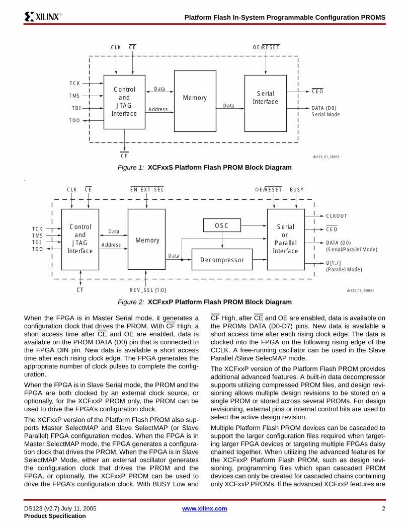
Platform Flash In-System Programmable Configuration PROMS
DS123 (v27) July 11 2005 wwwxilinxcom 2Product Specification
R
When the FPGA is in Master Serial mode it generates aconfiguration clock that drives the PROM With CF High ashort access time after CE and OE are enabled data isavailable on the PROM DATA (D0) pin that is connected tothe FPGA DIN pin New data is available a short accesstime after each rising clock edge The FPGA generates theappropriate number of clock pulses to complete the config-uration When the FPGA is in Slave Serial mode the PROM and theFPGA are both clocked by an external clock source oroptionally for the XCFxxP PROM only the PROM can beused to drive the FPGArsquos configuration clockThe XCFxxP version of the Platform Flash PROM also sup-ports Master SelectMAP and Slave SelectMAP (or SlaveParallel) FPGA configuration modes When the FPGA is inMaster SelectMAP mode the FPGA generates a configura-tion clock that drives the PROM When the FPGA is in SlaveSelectMAP Mode either an external oscillator generatesthe configuration clock that drives the PROM and theFPGA or optionally the XCFxxP PROM can be used todrive the FPGArsquos configuration clock With BUSY Low and
CF High after CE and OE are enabled data is available onthe PROMs DATA (D0-D7) pins New data is available ashort access time after each rising clock edge The data isclocked into the FPGA on the following rising edge of theCCLK A free-running oscillator can be used in the SlaveParallel Slave SelecMAP modeThe XCFxxP version of the Platform Flash PROM providesadditional advanced features A built-in data decompressorsupports utilizing compressed PROM files and design revi-sioning allows multiple design revisions to be stored on asingle PROM or stored across several PROMs For designrevisioning external pins or internal control bits are used toselect the active design revisionMultiple Platform Flash PROM devices can be cascaded tosupport the larger configuration files required when target-ing larger FPGA devices or targeting multiple FPGAs daisychained together When utilizing the advanced features forthe XCFxxP Platform Flash PROM such as design revi-sioning programming files which span cascaded PROMdevices can only be created for cascaded chains containingonly XCFxxP PROMs If the advanced XCFxxP features are
Figure 1 XCFxxS Platform Flash PROM Block Diagram
Controland
JTAGInterface
MemorySerial
InterfaceDATA (D0)Serial Mode
Data
Address
CLK CE
TCK
TMS
TDI
TDO
OERESET
CEO
Data
ds123_01_30603CF
FI
Figure 2 XCFxxP Platform Flash PROM Block Diagram
CLKOUT
CEO
DATA (D0)(SerialParallel Mode)
D[17](Parallel Mode)
TCKTMSTDITDO
CLK CE EN_EXT_SEL OERESET BUSY
Data
Data
Address
REV_SEL [10]CF
Controland
JTAGInterface
Memory
OSC Serialor
ParallelInterface
Decompressor
ds123_19_050604
Platform Flash In-System Programmable Configuration PROMS
DS123 (v27) July 11 2005 wwwxilinxcom 3Product Specification
R
not enabled then the cascaded chain can include bothXCFxxP and XCFxxS PROMsThe Platform Flash PROMs are compatible with all of theexisting FPGA device families A reference list of XilinxFPGAs and the respective compatible Platform FlashPROMs is given in Table 2 A list of Platform Flash PROMsand their capacities is given in Table 3
Table 2 Xilinx FPGAs and Compatible Platform Flash PROMs
FPGAConfiguration
BitstreamPlatform Flash
PROM(1)
Virtex-4 LXXC4VLX15 4765568 XCF08P
XC4VLX25 7819904 XCF08P
XC4VLX40 12259712 XCF16P
XC4VLX60 17717632 XCF32P
XC4VLX80 23291008 XCF32P
XC4VLX100 30711680 XCF32P
XC4VLX160 40347008 XCF32P+XCF08P
XC4VLX200 51367808 XCF32P+XCF32P
Virtex-4 FXXC4VFX12 4765568 XCF08P
XC4VFX20 7242624 XCF08P
XC4VFX40 14936192 XCF16P
XC4VFX60 21002880 XCF32P
XC4VFX100 33065408 XCF32P
XC4VFX140 47856896 XCF32P+XCF16P
Virtex-4 SXXC4VSX25 9147648 XCF16P
XC4VSX35 13700288 XCF16P
XC4VSX55 22749184 XCF32P
Virtex-II Pro XXC2VPX20 8214560 XCF08P
XC2VPX70 26098976 XCF32P
Virtex-II ProXC2VP2 1305376 XCF02SXC2VP4 3006496 XCF04SXC2VP7 4485408 XCF08PXC2VP20 8214560 XCF08PXC2VP30 11589920 XCF16PXC2VP40 15868192 XCF16PXC2VP50 19021344 XCF32PXC2VP70 26098976 XCF32PXC2VP100 34292768 XCF32P(2)
Virtex-II (3)
XC2V40 360096 XCF01SXC2V80 635296 XCF01S
XC2V250 1697184 XCF02SXC2V500 2761888 XCF04SXC2V1000 4082592 XCF04SXC2V1500 5659296 XCF08PXC2V2000 7492000 XCF08PXC2V3000 10494368 XCF16PXC2V4000 15659936 XCF16PXC2V6000 21849504 XCF32PXC2V8000 29063072 XCF32PVirtex-EXCV50E 630048 XCF01SXCV100E 863840 XCF01SXCV200E 1442016 XCF02SXCV300E 1875648 XCF02SXCV400E 2693440 XCF04SXCV405E 3430400 XCF04SXCV600E 3961632 XCF04SXCV812E 6519648 XCF08PXCV1000E 6587520 XCF08PXCV1600E 8308992 XCF08PXCV2000E 10159648 XCF16PXCV2600E 12922336 XCF16PXCV3200E 16283712 XCF16PVirtexXCV50 559200 XCF01SXCV100 781216 XCF01SXCV150 1040096 XCF01SXCV200 1335840 XCF02SXCV300 1751808 XCF02SXCV400 2546048 XCF04SXCV600 3607968 XCF04SXCV800 4715616 XCF08PXCV1000 6127744 XCF08P
Spartan-3EXC3S100E 581344 XCF01S
XC3S250E 1352192 XCF02S
XC3S500E 2267136 XCF04S
XC3S1200E 3832320 XCF04S
XC3S1600E 5957760 XCF08P
Spartan-3LXC3S1000L 3223488 XCF04S
XC3S1500L 5214784 XCF08P
XC3S5000L 13271936 XCF16P
Table 2 Xilinx FPGAs and Compatible Platform Flash PROMs (Continued)
FPGAConfiguration
BitstreamPlatform Flash
PROM(1)
Platform Flash In-System Programmable Configuration PROMS
DS123 (v27) July 11 2005 wwwxilinxcom 4Product Specification
R
ProgrammingIn-System ProgrammingIn-System Programmable PROMs can be programmedindividually or two or more can be daisy-chained togetherand programmed in-system via the standard 4-pin JTAGprotocol as shown in Figure 3 In-system programmingoffers quick and efficient design iterations and eliminatesunnecessary package handling or socketing of devices The
programming data sequence is delivered to the deviceusing either Xilinx iMPACT software and a Xilinx downloadcable a third-party JTAG development system aJTAG-compatible board tester or a simple microprocessorinterface that emulates the JTAG instruction sequence TheiMPACT software also outputs serial vector format (SVF)files for use with any tools that accept SVF format includingautomatic test equipment During in-system programmingthe CEO output is driven High All other outputs are held ina high-impedance state or held at clamp levels duringin-system programming In-system programming is fullysupported across the recommended operating voltage andtemperature ranges
OERESETThe 124 Mbit XCFxxS Platform Flash PROMs in-systemprogramming algorithm results in issuance of an internaldevice reset that causes OERESET to pulse Low
External ProgrammingXilinx reprogrammable PROMs can also be programmed bythe Xilinx MultiPRO Desktop Tool or a third-party deviceprogrammer This provides the added flexibility of usingpre-programmed devices with an in-system programmableoption for future enhancements and design changes
Reliability and EnduranceXilinx in-system programmable products provide a guaran-teed endurance level of 20000 in-system programerasecycles and a minimum data retention of 20 years Eachdevice meets all functional performance and data retentionspecifications within this endurance limit
Design SecurityThe Xilinx in-system programmable Platform Flash PROMdevices incorporate advanced data security features to fullyprotect the FPGA programming data against unauthorizedreading via JTAG The XCFxxP PROMs can also be pro-
Spartan-3XC3S50 439264 XCF01SXC3S200 1047616 XCF01SXC3S400 1699136 XCF02SXC3S1000 3223488 XCF04SXC3S1500 5214784 XCF08PXC3S2000 7673024 XCF08PXC3S4000 11316864 XCF16PXC3S5000 13271936 XCF16PSpartan-IIEXC2S50E 630048 XCF01SXC2S100E 863840 XCF01SXC2S150E 1134496 XCF02SXC2S200E 1442016 XCF02SXC2S300E 1875648 XCF02SXC2S400E 2693440 XCF04SXC2S600E 3961632 XCF04SSpartan-IIXC2S15 197696 XCF01SXC2S30 336768 XCF01SXC2S50 559200 XCF01SXC2S100 781216 XCF01SXC2S150 1040096 XCF01SXC2S200 1335840 XCF02S
Notes 1 If design revisioning or other advanced feature support is required
the XCFxxP can be used as an alternative to the XCF01S XCF02S or XCF04S
2 Assumes compression used3 The largest possible Virtex-II bitstream sizes are specified Refer to
the Virtex-II User Guide for information on bitgen options which affect bitstream size
Table 3 Platform Flash PROM CapacityPlatform
Flash PROMConfiguration
BitsPlatform Flash
PROMConfiguration
Bits
XCF01S 1048576 XCF08P 8388608XCF02S 2097152 XCF16P 16777216XCF04S 4194304 XCF32P 33554432
Table 2 Xilinx FPGAs and Compatible Platform Flash PROMs (Continued)
FPGAConfiguration
BitstreamPlatform Flash
PROM(1)
Figure 3 JTAG In-System Programming Operation(a) Solder Device to PCB (b) Program Using Download Cable
DS026_02_082703
GND
V CC
(a) (b)
huffman
XC3S2000 7673024 XCF08P
huffman
XCF08P 8388608
Platform Flash In-System Programmable Configuration PROMS
DS123 (v27) July 11 2005 wwwxilinxcom 5Product Specification
R
grammed to prevent inadvertent writing via JTAG Table 4and Table 5 show the security settings available for theXCFxxS PROM and XCFxxP PROM respectively
Read ProtectionThe read protect security bit can be set by the user to pre-vent the internal programming pattern from being read orcopied via JTAG Read protection does not prevent writeoperations For the XCFxxS PROM the read protect secu-rity bit is set for the entire device and resetting the read pro-tect security bit requires erasing the entire device For theXCFxxP PROM the read protect security bit can be set forindividual design revisions and resetting the read protectbit requires erasing the particular design revision
Write ProtectionThe XCFxxP PROM device also allows the user to writeprotect (or lock) a particular design revision to prevent inad-vertent erase or program operations Once set the writeprotect security bit for an individual design revision must bereset (using the UNLOCK command followed byISC_ERASE command) before an erase or program opera-tion can be performed
IEEE 11491 Boundary-Scan (JTAG)The Platform Flash PROM family is IEEE Standard 1532in-system programming compatible and is fully compliantwith the IEEE Std 11491 Boundary-Scan also known asJTAG which is a subset of IEEE Std 1532 Boundary-ScanA Test Access Port (TAP) and registers are provided to sup-port all required boundary scan instructions as well asmany of the optional instructions specified by IEEE Std11491 In addition the JTAG interface is used to implementin-system programming (ISP) to facilitate configuration era-sure and verification operations on the Platform FlashPROM device Table 6 lists the required and optionalboundary-scan instructions supported in the Platform FlashPROMs Refer to the IEEE Std 11491 specification for acomplete description of boundary-scan architecture and therequired and optional instructions
Instruction RegisterThe Instruction Register (IR) for the Platform Flash PROMis connected between TDI and TDO during an instructionscan sequence In preparation for an instruction scansequence the instruction register is parallel loaded with afixed instruction capture pattern This pattern is shifted outonto TDO (LSB first) while an instruction is shifted into theinstruction register from TDI
XCFxxS Instruction Register (8 bits wide)The Instruction Register (IR) for the XCFxxS PROM is eightbits wide and is connected between TDI and TDO during aninstruction scan sequence The detailed composition of theinstruction capture pattern is illustrated in Figure 4 Theinstruction capture pattern shifted out of the XCFxxS deviceincludes IR[70] IR[75] are reserved bits and are set to alogic 0 The ISC Status field IR[4] contains logic 1 if thedevice is currently in In-System Configuration (ISC) modeotherwise it contains logic 0 The Security field IR[3]contains logic 1 if the device has been programmed withthe security option turned on otherwise it contains logic0 IR[2] is unused and is set to 0 The remaining bitsIR[10] are set to 01 as defined by IEEE Std 11491
XCFxxP Instruction Register (16 bits wide)The Instruction Register (IR) for the XCFxxP PROM is six-teen bits wide and is connected between TDI and TDO dur-ing an instruction scan sequence The detailed compositionof the instruction capture pattern is illustrated in Figure 5The instruction capture pattern shifted out of the XCFxxPdevice includes IR[150] IR[159] are reserved bits and areset to a logic 0 The ISC Error field IR[87] contains a 10when an ISC operation is a success otherwise a 01 whenan In-System Configuration (ISC) operation fails TheEraseProgram (ERPROG) Error field IR[65] contains a10 when an erase or program operation is a success oth-
Table 4 XCFxxS Device Data Security Options
Read ProtectReadVerify
InhibitedProgram Inhibited
Erase Inhibited
Reset (default)
Set radic
Table 5 XCFxxP Design Revision Data Security Options
Read Protect Write ProtectReadVerify
InhibitedProgram Inhibited Erase Inhibited
Reset (default) Reset (default)
Reset (default) Set radic radic
Set Reset (default) radic
Set Set radic radic radic
Platform Flash In-System Programmable Configuration PROMS
DS123 (v27) July 11 2005 wwwxilinxcom 6Product Specification
R
erwise a 01 when an erase or program operation fails TheEraseProgram (ERPROG) Status field IR[4] contains alogic 1 when the device is busy performing an erase orprogramming operation otherwise it contains a logic 0The ISC Status field IR[3] contains logic 1 if the device iscurrently in In-System Configuration (ISC) mode otherwise
it contains logic 0 The DONE field IR[2] contains logic1 if the sampled design revision has been successfullyprogrammed otherwise a logic 0 indicates incompleteprogramming The remaining bits IR[10] are set to 01 asdefined by IEEE Std 11491
Boundary Scan RegisterThe boundary-scan register is used to control and observethe state of the device pins during the EXTEST SAM-PLEPRELOAD and CLAMP instructions Each output pinon the Platform Flash PROM has two register stages whichcontribute to the boundary-scan register while each inputpin has only one register stage The bidirectional pins havea total of three register stages which contribute to theboundary-scan register For each output pin the register
stage nearest to TDI controls and observes the output stateand the second stage closest to TDO controls and observesthe High-Z enable state of the output pin For each input pina single register stage controls and observes the input stateof the pin The bidirectional pin combines the three bits theinput stage bit is first followed by the output stage bit andfinally the output enable stage bit The output enable stagebit is closest to TDO
Table 6 Platform Flash PROM Boundary Scan Instructions
Boundary-Scan CommandXCFxxS IR[70]
(hex)XCFxxP IR[150]
(hex) Instruction Description
Required Instructions
BYPASS FF FFFF Enables BYPASS
SAMPLEPRELOAD 01 0001 Enables boundary-scan SAMPLEPRELOAD operation
EXTEST 00 0000 Enables boundary-scan EXTEST operation
Optional Instructions
CLAMP FA 00FA Enables boundary-scan CLAMP operation
HIGHZ FC 00FCPlaces all outputs in high-impedance state simultaneously
IDCODE FE 00FE Enables shifting out 32-bit IDCODE
USERCODE FD 00FD Enables shifting out 32-bit USERCODE
Platform Flash PROM Specific Instructions
CONFIG EE 00EE
Initiates FPGA configuration by pulsing CF pin Low once (For the XCFxxP this command also resets the selected design revision based on either the external REV_SEL[10] pins or on the internal design revision selection bits)(1)
Notes 1 For more information see Initiating FPGA Configuration
TDI rarr IR[75] IR[4] IR[3] IR[2] IR[10]
rarr TDOReserved ISC Status Security 0 0 1
Figure 4 XCFxxS Instruction Capture Values Loaded into IR as part of an Instruction Scan Sequence
TDI rarr IR[159] IR[87] IR[65] IR[4] IR[3] IR[2] IR[10]
rarr TDOReserved ISC Error ERPROG
ErrorERPROG
Status ISC Status DONE 0 1
Figure 5 XCFxxP Instruction Capture Values Loaded into IR as part of an Instruction Scan Sequence
Platform Flash In-System Programmable Configuration PROMS
DS123 (v27) July 11 2005 wwwxilinxcom 7Product Specification
R
See the XCFxxSXCFxxP Pin Names and DescriptionsTables in the Pinouts and Pin Descriptions section for theboundary-scan bit order for all connected device pins orsee the appropriate BSDL file for the complete bound-ary-scan bit order description under the attributeBOUNDARY_REGISTER section in the BSDL file The bitassigned to boundary-scan cell 0 is the LSB in the bound-ary-scan register and is the register bit closest to TDO
Identification RegistersIDCODE RegisterThe IDCODE is a fixed vendor-assigned value that is usedto electrically identify the manufacturer and type of thedevice being addressed The IDCODE register is 32 bitswide The IDCODE register can be shifted out for examina-tion by using the IDCODE instruction The IDCODE is avail-able to any other system component via JTAG Table 7 liststhe IDCODE register values for the Platform Flash PROMsThe IDCODE register has the following binary format
vvvvffffffffaaaaaaaaccccccccccc1
wherev = the die version numberf = the PROM family codea = the specific Platform Flash PROM product IDc = the Xilinx manufacturers IDThe LSB of the IDCODE register is always read as logic 1as defined by IEEE Std 11491
USERCODE RegisterThe USERCODE instruction gives access to a 32-bit userprogrammable scratch pad typically used to supply informa-tion about the devices programmed contents By using theUSERCODE instruction a user-programmable identifica-tion code can be shifted out for examination This code isloaded into the USERCODE register during programming ofthe Platform Flash PROM If the device is blank or was notloaded during programming the USERCODE register con-tains FFFFFFFFh
Customer Code RegisterFor the XCFxxP Platform Flash PROM in addition to theUSERCODE a unique 32-byte Customer Code can beassigned to each design revision enabled for the PROMThe Customer Code is set during programming and is typ-ically used to supply information about the design revisioncontents A private JTAG instruction is required to read theCustomer Code If the PROM is blank or the CustomerCode for the selected design revision was not loaded duringprogramming or if the particular design revision is erasedthe Customer Code will contain all ones
Platform Flash PROM TAP CharacteristicsThe Platform Flash PROM family performs both in-systemprogramming and IEEE 11491 boundary-scan (JTAG) test-ing via a single 4-wire Test Access Port (TAP) This simpli-fies system designs and allows standard Automatic TestEquipment to perform both functions The AC characteris-tics of the Platform Flash PROM TAP are described as fol-lows
TAP TimingFigure 6 shows the timing relationships of the TAP signalsThese TAP timing characteristics are identical for bothboundary-scan and ISP operations
Table 7 IDCODES Assigned to Platform Flash PROMsDevice IDCODE(1) (hex)
XCF01S ltvgt5044093
XCF02S ltvgt5045093
XCF04S ltvgt5046093
XCF08P ltvgt5057093
XCF16P ltvgt5058093
XCF32P ltvgt5059093
Notes 1 The ltvgt in the IDCODE field represents the devicersquos revision
code (in hex) and may vary
huffman
XCF08P ltvgt5057093
Platform Flash In-System Programmable Configuration PROMS
DS123 (v27) July 11 2005 wwwxilinxcom 8Product Specification
R
TAP AC ParametersTable 8 shows the timing parameters for the TAP waveforms shown in Figure 6
Additional Features for the XCFxxPInternal OscillatorThe 81632 Mbit XCFxxP Platform Flash PROMs includean optional internal oscillator which can be used to drive theCLKOUT and DATA pins on FPGA configuration interfaceThe internal oscillator can be enabled when programmingthe PROM and the oscillator can be set to either the defaultfrequency or to a slower frequency (AC CharacteristicsOver Operating Conditions When Cascading)
CLKOUTThe 81632 Mbit XCFxxP Platform Flash PROMs includethe programmable option to enable the CLKOUT signalwhich allows the PROM to provide a source synchronousclock aligned to the data on the configuration interface TheCLKOUT signal is derived from one of two clock sourcesthe CLK input pin or the internal oscillator The input clocksource is selected during the PROM programmingsequence Output data is available on the rising edge ofCLKOUT
The CLKOUT signal is enabled during programming and isactive when CE is Low and OERESET is High When dis-abled the CLKOUT pin is put into a high-impedance stateand should be pulled High externally to provide a knownstate When cascading Platform Flash PROMs with CLKOUTenabled after completing its data transfer the first PROMdisables CLKOUT and drives the CEO pin enabling the nextPROM in the PROM chain The next PROM will begin driv-ing the CLKOUT signal once that PROM is enabled anddata is available for transferDuring high-speed parallel configuration without compres-sion the FPGA drives the BUSY signal on the configurationinterface When BUSY is asserted High the PROMs inter-nal address counter stops incrementing and the currentdata value is held on the data outputs While BUSY is Highthe PROM will continue driving the CLKOUT signal to theFPGA clocking the FPGArsquos configuration logic When theFPGA deasserts BUSY indicating that it is ready to receiveadditional configuration data the PROM will begin drivingnew data onto the configuration interface
Figure 6 Test Access Port Timing
TCK
TCKMIN
TMSS
TMS
TDI
TDO
TMSH
TDIH
TDOV
TDIS
DS026_04_020300
Table 8 Test Access Port Timing ParametersSymbol Description Min Max Units
TCKMIN TCK minimum clock period when VCCJ = 25V or 33V 100 - ns
TMSS TMS setup time when VCCJ = 25V or 33V 10 - ns
TMSH TMS hold time when VCCJ = 25V or 33V 25 - ns
TDIS TDI setup time when VCCJ = 25V or 33V 10 - ns
TDIH TDI hold time when VCCJ = 25V or 33V 25 - ns
TDOV TDO valid delay when VCCJ = 25V or 33V - 30 ns
Platform Flash In-System Programmable Configuration PROMS
DS123 (v27) July 11 2005 wwwxilinxcom 9Product Specification
R
DecompressionThe 81632 Mbit XCFxxP Platform Flash PROMs include abuilt-in data decompressor compatible with Xilinx advancedcompression technology Compressed Platform FlashPROM files are created from the target FPGA bitstream(s)using the iMPACT software Only Slave Serial and SlaveSelectMAP (parallel) configuration modes are supported forFPGA configuration when using a XCFxxP PROM pro-grammed with a compressed bitstream Compression rateswill vary depending on several factors including the targetdevice family and the target design contentsThe decompression option is enabled during the PROMprogramming sequence The PROM decompresses thestored data before driving both clock and data onto theFPGAs configuration interface If Decompression isenabled then the Platform Flash clock output pin (CLK-
OUT) must be used as the clock signal for the configurationinterface driving the target FPGAs configuration clockinput pin (CCLK) Either the PROMs CLK input pin or theinternal oscillator must be selected as the source for CLK-OUT Any target FPGA connected to the PROM must oper-ate as slave in the configuration chain with theconfiguration mode set to Slave Serial mode or SlaveSelectMap (parallel) mode When decompression is enabled the CLKOUT signalbecomes a controlled clock output with a reduced maximumfrequency When decompressed data is not ready the CLK-OUT pin is put into a high-Z state and must be pulled Highexternally to provide a known stateThe BUSY input is automatically disabled when decom-pression is enabled
Design RevisioningDesign Revisioning allows the user to create up to fourunique design revisions on a single PROM or stored acrossmultiple cascaded PROMs Design Revisioning is sup-ported for the 81632 Mbit XCFxxP Platform Flash PROMsin both serial and parallel modes Design Revisioning canbe used with compressed PROM files and also when theCLKOUT feature is enabled The PROM programming filesalong with the revision information files (cfi) are createdusing the iMPACT software The cfi file is required toenable design revision programming in iMPACT A single design revision is composed of from 1 to n 8-Mbitmemory blocks If a single design revision contains lessthan 8 Mbits of data then the remaining space is paddedwith all ones A larger design revision can span several8-Mbit memory blocks and any space remaining in the last8-Mbit memory block is padded with all ones bull A single 32-Mbit PROM contains four 8-Mbit memory
blocks and can therefore store up to four separate design revisions one 32-Mbit design revision two 16-Mbit design revisions three 8-Mbit design revisions four 8-Mbit design revisions and so on
bull Because of the 8-Mbit minimum size requirement for each revision a single 16-Mbit PROM can only store up to two separate design revisions one 16-Mbit design revision one 8-Mbit design revision or two 8-Mbit design revisions
bull A single 8-Mbit PROM can store only one 8-Mbit design revision
Larger design revisions can be split over several cascadedPROMs For example two 32-Mbit PROMs can store up tofour separate design revisions one 64-Mbit design revisiontwo 32-Mbit design revisions three 16-Mbit design revi-sions four 16-Mbit design revisions and so on When cas-
cading one 16-Mbit PROM and one 8-Mbit PROM there are24 Mbits of available space and therefore up to three sepa-rate design revisions can be stored one 24-Mbit designrevision two 8-Mbit design revisions or three 8-Mbit designrevisions See Figure 7 for a few basic examples of how multiple revi-sions can be stored The design revision partitioning is han-dled automatically during file generation in iMPACT During the PROM file creation each design revision isassigned a revision number
Revision 0 = 00 Revision 1 = 01Revision 2 = 10Revision 3 = 11
After programming the Platform Flash PROM with a set ofdesign revisions a particular design revision can beselected using the external REV_SEL[10] pins or using theinternal programmable design revision control bits TheEN_EXT_SEL pin determines if the external pins or internalbits are used to select the design revision WhenEN_EXT_SEL is Low design revision selection is controlledby the external Revision Select pins REV_SEL[10] WhenEN_EXT_SEL is High design revision selection is con-trolled by the internal programmable Revision Select controlbits During power up the design revision selection inputs(pins or control bits) are sampled internally After power upwhen CE is asserted (Low) enabling the PROM inputs thedesign revision selection inputs are sampled again after therising edge of the CF pulse The data from the selecteddesign revision is then presented on the FPGA configura-tion interface
Platform Flash In-System Programmable Configuration PROMS
DS123 (v27) July 11 2005 wwwxilinxcom 10Product Specification
R
PROM to FPGA Configuration Mode and Connections SummaryThe FPGAs IO logical functions and internal interconnec-tions are established by the configuration data contained inthe FPGArsquos bitstream The bitstream is loaded into theFPGA either automatically upon power up or on commanddepending on the state of the FPGAs mode pins XilinxPlatform Flash PROMs are designed to download directly tothe FPGA configuration interface FPGA configurationmodes which are supported by the XCFxxS Platform FlashPROMs include Master Serial and Slave Serial FPGA con-figuration modes which are supported by the XCFxxP Plat-form Flash PROMs include Master Serial Slave SerialMaster SelectMAP and Slave SelectMAP Below is a shortsummary of the supported FPGA configuration modes Seethe respective FPGA data sheet for device configurationdetails including which configuration modes are supportedby the targeted FPGA device
FPGA Master Serial ModeIn Master Serial mode the FPGA automatically loads theconfiguration bitstream in bit-serial form from external mem-ory synchronized by the configuration clock (CCLK) gener-ated by the FPGA Upon power-up or reconfiguration theFPGAs mode select pins are used to select the MasterSerial configuration mode Master Serial Mode provides asimple configuration interface Only a serial data line aclock line and two control lines (INIT and DONE) arerequired to configure an FPGA Data from the PROM isread out sequentially on a single data line (DIN) accessedvia the PROMs internal address counter which is incre-mented on every valid rising edge of CCLK The serial bit-stream data must be set up at the FPGArsquos DIN input pin ashort time before each rising edge of the FPGAs internallygenerated CCLK signal
Figure 7 Design Revision Storage Examples
REV 0(8 Mbits)
REV 1(8 Mbits)
REV 2(8 Mbits)
REV 3(8 Mbits)
REV 0(8 Mbits)
REV 1(8 Mbits)
REV 2(16 Mbits)
REV 0(16 Mbits)
REV 1(16 Mbits)
REV 0(8 Mbits)
REV 1(24 Mbits)
REV 0(32 Mbits)
4 Design Revisions 3 Design Revisions 2 Design Revisions 1 Design Revision
(a) Design Revision storage examples for a single XCF32P PROM
REV 0(16 Mbits)
REV 1(16 Mbits)
REV 2(16 Mbits)
REV 3(16 Mbits)
REV 0(16 Mbits)
REV 1(16 Mbits)
REV 2(32 Mbits)
REV 0(32 Mbits)
REV 1(32 Mbits)
REV 0(16 Mbits)
REV 1(16 Mbits)
REV 0(32 Mbits)
4 Design Revisions 3 Design Revisions 2 Design Revisions 1 Design Revision
(b) Design Revision storage examples spanning two XCF32P PROMs
PROM 0 PROM 0 PROM 0 PROM 0 PROM 0
PROM 0 PROM 0 PROM 0 PROM 0 PROM 0
REV 0(32 Mbits)
REV 1(32 Mbits)
PROM 1 PROM 1 PROM 1 PROM 1 PROM 1
ds123_20_102103
Platform Flash In-System Programmable Configuration PROMS
DS123 (v27) July 11 2005 wwwxilinxcom 11Product Specification
R
Typically a wide range of frequencies can be selected forthe FPGArsquos internally generated CCLK which always startsat a slow default frequency The FPGArsquos bitstream containsconfiguration bits which can switch CCLK to a higher fre-quency for the remainder of the Master Serial configurationsequence The desired CCLK frequency is selected duringbitstream generationConnecting the FPGA device to the configuration PROM forMaster Serial Configuration Mode (Figure 8)bull The DATA output of the PROM(s) drive the DIN input of
the lead FPGA devicebull The Master FPGA CCLK output drives the CLK input(s)
of the PROM(s) bull The CEO output of a PROM drives the CE input of the
next PROM in a daisy chain (if any)bull The OERESET pins of all PROMs are connected to
the INIT_B pins of all FPGA devices This connection assures that the PROM address counter is reset before the start of any (re)configuration
bull The PROM CE input can be driven from the DONE pin The CE input of the first (or only) PROM can be driven by the DONE output of all target FPGA devices provided that DONE is not permanently grounded CE can also be permanently tied Low but this keeps the DATA output active and causes an unnecessary ICC active supply current (DC Characteristics Over Operating Conditions)
bull The PROM CF pin is typically connected to the FPGAs PROG_B (or PROGRAM) input For the XCFxxP only the CF pin is a bidirectional pin If the XCFxxP CF pin is not connected to the FPGAs PROG_B (or PROGRAM) input then the pin should be tied High
FPGA Slave Serial ModeIn Slave Serial mode the FPGA loads the configuration bit-stream in bit-serial form from external memory synchro-nized by an externally supplied clock Upon power-up orreconfiguration the FPGAs mode select pins are used toselect the Slave Serial configuration mode Slave SerialMode provides a simple configuration interface Only aserial data line a clock line and two control lines (INIT andDONE) are required to configure an FPGA Data from thePROM is read out sequentially on a single data line (DIN)accessed via the PROMs internal address counter which isincremented on every valid rising edge of CCLK The serialbitstream data must be set up at the FPGArsquos DIN input pin ashort time before each rising edge of the externally providedCCLKConnecting the FPGA device to the configuration PROM forSlave Serial Configuration Mode (Figure 9)bull The DATA output of the PROM(s) drive the DIN input of
the lead FPGA devicebull The PROM CLKOUT (for XCFxxP only) or an external
clock source drives the FPGAs CCLK input
bull The CEO output of a PROM drives the CE input of the next PROM in a daisy chain (if any)
bull The OERESET pins of all PROMs are connected to the INIT_B (or INIT) pins of all FPGA devices This connection assures that the PROM address counter is reset before the start of any (re)configuration
bull The PROM CE input can be driven from the DONE pin The CE input of the first (or only) PROM can be driven by the DONE output of all target FPGA devices provided that DONE is not permanently grounded CE can also be permanently tied Low but this keeps the DATA output active and causes an unnecessary ICC active supply current (DC Characteristics Over Operating Conditions)
bull The PROM CF pin is typically connected to the FPGAs PROG_B (or PROGRAM) input For the XCFxxP only the CF pin is a bidirectional pin If the XCFxxP CF pin is not connected to the FPGAs PROG_B (or PROGRAM) input then the pin should be tied High
Serial Daisy ChainMultiple FPGAs can be daisy-chained for serial configura-tion from a single source After a particular FPGA has beenconfigured the data for the next device is routed internallyto the FPGArsquos DOUT pin Typically the data on the DOUTpin changes on the falling edge of CCLK although for somedevices the DOUT pin changes on the rising edge of CCLKConsult the respective device data sheets for detailed infor-mation on a particular FPGA device For clocking thedaisy-chained configuration either the first FPGA in thechain can be set to Master Serial generating the CCLKwith the remaining devices set to Slave Serial (Figure 10)or all the FPGA devices can be set to Slave Serial and anexternally generated clock can be used to drive the FPGAsconfiguration interface
FPGA Master SelectMAP (Parallel) Mode(1)
In Master SelectMAP mode byte-wide data is written intothe FPGA typically with a BUSY flag controlling the flow ofdata synchronized by the configuration clock (CCLK) gen-erated by the FPGA Upon power-up or reconfiguration theFPGAs mode select pins are used to select the MasterSelectMAP configuration mode The configuration interfacetypically requires a parallel data bus a clock line and twocontrol lines (INIT and DONE) In addition the FPGArsquos ChipSelect Write and BUSY pins must be correctly controlled toenable SelectMAP configuration The configuration data isread from the PROM byte by byte on pins [D0D7]accessed via the PROMs internal address counter which isincremented on every valid rising edge of CCLK The bit-stream data must be set up at the FPGArsquos [D0D7] input
1 The Master SelectMAP (Parallel) FPGA configuration mode is sup-ported only by the XCFxxP Platform Flash PROM This mode is not supported by the XCFxxS Platform Flash PROM
Platform Flash In-System Programmable Configuration PROMS
DS123 (v27) July 11 2005 wwwxilinxcom 12Product Specification
R
pins a short time before each rising edge of the FPGAsinternally generated CCLK signal If BUSY is asserted(High) by the FPGA the configuration data must be helduntil BUSY goes Low An external data source or externalpull-down resistors must be used to enable the FPGAsactive Low Chip Select (CS or CS_B) and Write (WRITE orRDWR_B) signals to enable the FPGAs SelectMAP config-uration process The Master SelectMAP configuration interface is clocked bythe FPGArsquos internal oscillator Typically a wide range of fre-quencies can be selected for the internally generated CCLKwhich always starts at a slow default frequency The FPGArsquosbitstream contains configuration bits which can switchCCLK to a higher frequency for the remainder of the MasterSelectMAP configuration sequence The desired CCLK fre-quency is selected during bitstream generationAfter configuration the pins of the SelectMAP port can beused as additional user IO Alternatively the port can beretained using the persist optionConnecting the FPGA device to the configuration PROM forMaster SelectMAP (Parallel) Configuration Mode(Figure 11)bull The DATA outputs of the PROM(s) drive the [D0D7]
input of the lead FPGA devicebull The Master FPGA CCLK output drives the CLK input(s)
of the PROM(s) bull The CEO output of a PROM drives the CE input of the
next PROM in a daisy chain (if any)bull The OERESET pins of all PROMs are connected to
the INIT_B pins of all FPGA devices This connection assures that the PROM address counter is reset before the start of any (re)configuration
bull The PROM CE input can be driven from the DONE pin The CE input of the first (or only) PROM can be driven by the DONE output of all target FPGA devices provided that DONE is not permanently grounded CE can also be permanently tied Low but this keeps the DATA output active and causes an unnecessary ICC active supply current (DC Characteristics Over Operating Conditions)
bull For high-frequency parallel configuration the BUSY pins of all PROMs are connected to the FPGAs BUSY output This connection assures that the next data transition for the PROM is delayed until the FPGA is ready for the next configuration data byte
bull The PROM CF pin is typically connected to the FPGAs PROG_B (or PROGRAM) input For the XCFxxP only the CF pin is a bidirectional pin If the XCFxxP CF pin is not connected to the FPGAs PROG_B (or PROGRAM) input then the pin should be tied High
FPGA Slave SelectMAP (Parallel) Mode(1)
In Slave SelectMAP mode byte-wide data is written into theFPGA typically with a BUSY flag controlling the flow of
data synchronized by an externally supplied configurationclock (CCLK) Upon power-up or reconfiguration theFPGAs mode select pins are used to select the SlaveSelectMAP configuration mode The configuration interfacetypically requires a parallel data bus a clock line and twocontrol lines (INIT and DONE) In addition the FPGArsquos ChipSelect Write and BUSY pins must be correctly controlled toenable SelectMAP configuration The configuration data isread from the PROM byte by byte on pins [D0D7]accessed via the PROMs internal address counter which isincremented on every valid rising edge of CCLK The bit-stream data must be set up at the FPGArsquos [D0D7] inputpins a short time before each rising edge of the providedCCLK If BUSY is asserted (High) by the FPGA the config-uration data must be held until BUSY goes Low An externaldata source or external pull-down resistors must be used toenable the FPGAs active Low Chip Select (CS or CS_B)and Write (WRITE or RDWR_B) signals to enable theFPGAs SelectMAP configuration process After configuration the pins of the SelectMAP port can beused as additional user IO Alternatively the port can beretained using the persist optionConnecting the FPGA device to the configuration PROM forSlave SelectMAP (Parallel) Configuration Mode(Figure 12)bull The DATA outputs of the PROM(s) drives the [D0D7]
inputs of the lead FPGA devicebull The PROM CLKOUT (for XCFxxP only) or an external
clock source drives the FPGAs CCLK inputbull The CEO output of a PROM drives the CE input of the
next PROM in a daisy chain (if any)bull The OERESET pins of all PROMs are connected to
the INIT_B pins of all FPGA devices This connection assures that the PROM address counter is reset before the start of any (re)configuration
bull The PROM CE input can be driven from the DONE pin The CE input of the first (or only) PROM can be driven by the DONE output of all target FPGA devices provided that DONE is not permanently grounded CE can also be permanently tied Low but this keeps the DATA output active and causes an unnecessary ICC active supply current (DC Characteristics Over Operating Conditions)
bull For high-frequency parallel configuration the BUSY pins of all PROMs are connected to the FPGAs BUSY output This connection assures that the next data transition for the PROM is delayed until the FPGA is ready for the next configuration data byte
bull The PROM CF pin is typically connected to the FPGAs
1 The Slave SelectMAP (Parallel) FPGA configuration mode is sup-ported only by the XCFxxP Platform Flash PROMsThis mode is not supported by the XCFxxS Platform Flash PROM
Platform Flash In-System Programmable Configuration PROMS
DS123 (v27) July 11 2005 wwwxilinxcom 13Product Specification
R
PROG_B (or PROGRAM) input For the XCFxxP only the CF pin is a bidirectional pin If the XCFxxP CF pin is not connected to the FPGAs PROG_B (or PROGRAM) input then the pin should be tied High
FPGA SelectMAP (Parallel) Device Chaining(1)
Multiple Virtex-II FPGAs can be configured using theSelectMAP mode and be made to start up simultaneouslyTo configure multiple devices in this way wire the individualCCLK DONE INIT Data ([D0D7]) Write (WRITE orRDWR_B) and BUSY pins of all the devices in parallel If alldevices are to be configured with the same bitstream read-back is not being used and the CCLK frequency selecteddoes not require the use of the BUSY signal the CS_B pinscan be connected to a common line so all of the devices areconfigured simultaneously (Figure 13)With additional control logic the individual devices can beloaded separately by asserting the CS_B pin of each devicein turn and then enabling the appropriate configuration dataThe PROM can also store the individual bitstreams for eachFPGA for SelectMAP configuration in separate design revi-sions When design revisioning is utilized additional controllogic can be used to select the appropriate bitstream byasserting the EN_EXT_SEL pin and using theREV_SEL[10] pins to select the required bitstream whileasserting the CS_B pin for the FPGA the bitstream is target-ing (Figure 14) For clocking the parallel configuration chain either the firstFPGA in the chain can be set to Master SelectMAP gener-ating the CCLK with the remaining devices set to SlaveSelectMAP or all the FPGA devices can be set to SlaveSelectMAP and an externally generated clock can be usedto drive the configuration interface Again the respectivedevice data sheets should be consulted for detailed infor-mation on a particular FPGA device including which config-uration modes are supported by the targeted FPGA device
Cascading Configuration PROMsWhen configuring multiple FPGAs in a serial daisy chainconfiguring multiple FPGAs in a SelectMAP parallel chainor configuring a single FPGA requiring a larger configura-tion bitstream cascaded PROMs provide additional mem-ory (Figure 10 Figure 13 Figure 14 and Figure 15)Multiple Platform Flash PROMs can be concatenated byusing the CEO output to drive the CE input of the down-stream device The clock signal and the data outputs of allPlatform Flash PROMs in the chain are interconnectedAfter the last data from the first PROM is read the firstPROM asserts its CEO output Low and drives its outputs to
a high-impedance state The second PROM recognizes theLow level on its CE input and immediately enables its out-putsAfter configuration is complete address counters of all cas-caded PROMs are reset if the PROM OERESET pin goesLow or CE goes HighWhen utilizing the advanced features for the XCFxxP Plat-form Flash PROM including the clock output (CLKOUT)option decompression option or design revisioning pro-gramming files which span cascaded PROM devices canonly be created for cascaded chains containing onlyXCFxxP PROMs If the advanced features are not usedthen cascaded PROM chains can contain both XCFxxP andXCFxxS PROMs
Initiating FPGA ConfigurationThe options for initiating FPGA configuration via the Plat-form Flash PROM include1 Automatic configuration on power up2 Applying an external PROG_B (or PROGRAM) pulse3 Applying the JTAG CONFIG instructionFollowing the FPGArsquos power-on sequence or the assertionof the PROG_B (or PROGRAM) pin the FPGArsquos configura-tion memory is cleared the configuration mode is selectedand the FPGA is ready to accept a new configuration bit-stream The FPGArsquos PROG_B pin can be controlled by anexternal source or alternatively the Platform Flash PROMsincorporate a CF pin that can be tied to the FPGArsquosPROG_B pin Executing the CONFIG instruction throughJTAG pulses the CF output Low once for 300-500 ns reset-ting the FPGA and initiating configuration The iMPACTsoftware can issue the JTAG CONFIG command to initiateFPGA configuration by setting the Load FPGA option When using the XCFxxP Platform Flash PROM with designrevisioning enabled the CF pin should always be con-nected to the PROG_B (or PROGRAM) pin on the FPGA toensure that the current design revision selection is sampledwhen the FPGA is reset The XCFxxP PROM samples thecurrent design revision selection from the externalREV_SEL pins or the internal programmable RevisionSelect bits on the rising edge of CF When the JTAG CON-FIG command is executed the XCFxxP will sample the newdesign revision before initiating the FPGA configurationsequence When using the XCFxxP Platform Flash PROMwithout design revisioning if the CF pin is not connected tothe FPGA PROG_B (or PROGRAM) pin then the XCFxxPCF pin should be tied High
1 The SelectMAP (Parallel) FPGA configuration modes are supported only by the XCFxxP Platform Flash PROMThese modes are not sup-ported by the XCFxxS Platform Flash PROM
Platform Flash In-System Programmable Configuration PROMS
DS123 (v27) July 11 2005 wwwxilinxcom 14Product Specification
R
Configuration PROM to FPGA Device Interface Connection Diagrams
Figure 8 Configuring in Master Serial Mode
Xilinx FPGAMaster Serial
DIN
CCLK
DONE
INIT_B
PROG_B
TDI
TMS
TCK
GND
MODE PINS(1)
DOUT
TDO
VCCJ VCCO VCCINT
DIN
CCLK
DONE
INIT_B
PROG_B
DIN
CCLK
DONE
INIT_B
PROG_B
47
kΩ
47
kΩ (1)
VCCO(2)
OPTIONALDaisy-chainedSlave FPGAs with differentconfigurations
OPTIONALSlave FPGAs with identicalconfigurations
TDI
TMS
TCK
TDO
Notes1 For Mode pin connections and DONE pin pullup value refer to the appropriate FPGA data sheet2 For compatible voltages refer to the appropriate data sheet3 For the XCFxxS the CF pin is an output pin For the XCFxxP the CF pin is a bidirectional pin
Platform Flash PROM
VCCINT
VCCO(2)
VCCJ(2)
TDI
TMS
TCK
GND
D0
CLK
CE
CEO
OERESET
CF(3)
TDO
ds123_11_100804
Platform Flash In-System Programmable Configuration PROMS
DS123 (v27) July 11 2005 wwwxilinxcom 15Product Specification
R
Figure 9 Configuring in Slave Serial Mode
Xilinx FPGASlave Serial
DIN
CCLK
DONE
INIT_B
PROG_B
TDI
TMS
TCK
GND
MODE PINS(1)
DOUT
TDO
VCCJ VCCO VCCINT
DIN
CCLK
DONE
INIT_B
PROG_B
DIN
CCLK
DONE
INIT_B
PROG_B
47
kΩ
47
kΩ (1)
VCCO(2)
OPTIONALDaisy-chainedSlave FPGAs with differentconfigurations
OPTIONALSlave FPGAs with identicalconfigurations
TDI
TMS
TCK
TDO
Notes1 For Mode pin connections and DONE pin pullup value refer to the appropriate FPGA data sheet2 For compatible voltages refer to the appropriate data sheet3 In Slave Serial mode the configuration interface can be clocked by an external oscillator or optionallymdashfor the XCFxxP Platform Flash PROM onlymdashthe CLKOUT signal can be used to drive the FPGAs configuration clock (CCLK) If the XCFxxP PROMs CLKOUT signal is used then it must be tied to a 47KΩ resistor pulled up to VCCO4 For the XCFxxS the CF pin is an output pin For the XCFxxP the CF pin is a bidirectional pin
Platform Flash PROM
VCCINT
VCCO(2)
VCCJ(2)
TDI
TMS
TCK
GND
D0
CLK(3)
CE
CEO
OERESET
CF(4)
TDO
ds123_12_070505
External (3)
Oscillator
Platform Flash In-System Programmable Configuration PROMS
DS123 (v27) July 11 2005 wwwxilinxcom 16Product Specification
R
Figure 10 Configuring Multiple Devices MasterSlave Serial Mode
Platform Flash PROM
First PROM(PROM 0)
VCCINT
VCCO(2)
VCCJ(2)
TDI
TMS
TCK
D0
CLK
CE
CEO
OERESET
CF(3)
TDO
Xilinx FPGAMaster Serial
DIN
CCLK
DONE
INIT_B
PROG_B
TDI
TMS
TCK
MODE PINS(1)
DOUT
TDO
VCCJ VCCO VCCINT
47
kΩ
47
kΩ (1)
VCCO(2)
TDI
TMS
TCK
TDO
Notes1 For Mode pin connections and DONE pin pullup value refer to the appropriate FPGA data sheet2 For compatible voltages refer to the appropriate data sheet3 For the XCFxxS the CF pin is an output pin For the XCFxxP the CF pin is a bidirectional pin
Xilinx FPGASlave Serial
DIN
CCLK
DONE
INIT_B
PROG_B
TDI
TMS
TCK
Platform Flash PROM
Cascaded PROM(PROM 1)
VCCINT
VCCO(2)
VCCJ(2)
TDI
TMS
TCK
D0
CLK
CE
CEO
OERESET
CF(3)
TDO
VCCJ VCCO VCCINT
MODE PINS(1)
TDO
ds123_13_100804
GND
GNDGND
GND
Platform Flash In-System Programmable Configuration PROMS
DS123 (v27) July 11 2005 wwwxilinxcom 17Product Specification
R
Figure 11 Configuring in Master SelectMAP Mode
XCFxxPPlatform Flash PROM
VCCINT
VCCO(2)
VCCJ(2)
TDI
TMS
TCK
GND
D[07]
CLK
CE
CEO
OERESET
CF(5)
BUSY(4)
TDO
Xilinx FPGAMaster SelectMAP
D[07]
CCLK
DONE
INIT_B
PROG_B
BUSY(4)
TDI
TMS
TCK
GND
MODE PINS(1)
RDWR_B
CS_B
TDO
VCCJ VCCO VCCINT
D[07]
CCLK
DONE
INIT_B
PROG_B
BUSY(4)
47
kΩ
47
kΩ (1)
VCCO(2)
OPTIONALSlave FPGAs with identicalconfigurations
TDI
TMS
TCK
TDO
Notes1 For Mode pin connections and DONE pin pullup value refer to the appropriate FPGA data sheet2 For compatible voltages refer to the appropriate data sheet3 CS_B (or CS) and RDWR_B (or WRITE) must be either driven Low or pulled down exernally One option is shown4 The BUSY pin is only available with the XCFxxP Platform Flash PROM and the connection is only required for high-frequency SelectMAP mode configuration For BUSY pin requirements refer to the appropriate FPGA data sheet5 For the XCFxxP the CF pin is a bidirectional pin
1KΩ
1KΩ
IO(3)
IO(3)
ds123_14_100804
Platform Flash In-System Programmable Configuration PROMS
DS123 (v27) July 11 2005 wwwxilinxcom 18Product Specification
R
Figure 12 Configuring in Slave SelectMAP Mode
XCFxxPPlatform Flash PROM
VCCINT
VCCO(2)
VCCJ(2)
TDI
TMS
TCK
GND
D[07]
CLK(5)
CE
CEO
OERESET
CF(6)
BUSY(4)
TDO
Xilinx FPGASlave SelectMAP
D[07]
CCLK
DONE
INIT_B
PROG_B
BUSY(4)
TDI
TMS
TCK
GND
MODE PINS(1)
RDWR_B
CS_B
TDO
VCCJ VCCO VCCINT
D[07]
CCLK
DONE
INIT_B
PROG_B
BUSY(4)
47
kΩ
47
kΩ (1)
VCCO(2)
OPTIONALSlave FPGAs with identicalconfigurations
TDI
TMS
TCK
TDO
Notes1 For Mode pin connections and DONE pin pullup value refer to the appropriate FPGA data sheet2 For compatible voltages refer to the appropriate data sheet3 CS_B (or CS) and RDWR_B (or WRITE) must be either driven Low or pulled down exernally One option is shown4 The BUSY pin is only available with the XCFxxP Platform Flash PROM and the connection is only required for high-frequency SelectMAP mode configuration For BUSY pin requirements refer to the appropriate FPGA data sheet5 In Slave SelectMAP mode the configuration interface can be clocked by an external oscillator or optionally the CLKOUT signal can be used to drive the FPGAs configuration clock (CCLK) If the XCFxxP PROMs CLKOUT signal is used then it must be tied to a 47KΩ resistor pulled up to VCCO6 For the XCFxxP the CF pin is a bidirectional pin
1KΩ
1KΩ
IO(3)
IO(3)
ds123_15_070505
External (5)
Oscillator
Platform Flash In-System Programmable Configuration PROMS
DS123 (v27) July 11 2005 wwwxilinxcom 19Product Specification
R
Figure 13 Configuring Multiple Devices with Identical Patterns in MasterSlave SelectMAP Mode
XCFxxPPlatform Flash PROM
First PROM(PROM 0)
VCCINT
VCCO(2)
VCCJ(2)
TDI
TMS
TCK
GND
D[07]
CLK
CE
CEO
OERESET
CF(5)
BUSY(4)
TDO
Xilinx FPGAMaster SelectMAP
D[07]
CCLK
DONE
INIT_B
PROG_B
BUSY(4)
TDI
TMS
TCK
GND
MODE PINS(1)
TDO
VCCJ VCCO VCCINT
47
kΩ
47
kΩ (1)
VCCO(2)
TDI
TMS
TCK
TDO
Notes1 For Mode pin connections and DONE pin pullup value refer to the appropriate FPGA data sheet2 For compatible voltages refer to the appropriate data sheet3 CS_B (or CS) and RDWR_B (or WRITE) must be either driven Low or pulled down exernally One option is shown4 The BUSY pin is only available with the XCFxxP Platform Flash PROM and the connection is only required for high-frequency SelectMAP mode configuration For BUSY pin requirements refer to the appropriate FPGA data sheet5 For the XCFxxP the CF pin is a bidirectional pin
Xilinx FPGASlave SelectMAP
D[07]
CCLK
DONE
INIT_B
PROG_B
BUSY(4)
TDI
TMS
TCK
GND
XCFxxPPlatform Flash PROM
Cascaded PROM(PROM 1)
VCCINT
VCCO(2)
VCCJ(2)
TDI
TMS
TCK
GND
D[07]
CLK
CE
CEO
OERESET
CF(5)
BUSY(4)
TDO
VCCJ VCCO VCCINT
MODE PINS(1)
TDO
ds123_16_100804
1KΩ1K
Ω
IO(3)
IO(3)
1KΩ1K
Ω
IO(3)
IO(3)RDWR_B
CS_B
RDWR_B
CS_B
Platform Flash In-System Programmable Configuration PROMS
DS123 (v27) July 11 2005 wwwxilinxcom 20Product Specification
R
Figure 14 Configuring Multiple Devices with Design Revisioning in Slave Serial Mode
XCFxxPPlatform Flash PROM
First PROM(PROM 0)
VCCINT
VCCO(2)
VCCJ(2)
TDI
TMS
TCK
EN_EXT_SEL
REV_SEL[10]
D0
CLK(3)
CE
CEO
OERESET
CF(4)
TDO
Xilinx FPGASlave Serial
DIN
CCLK
DONE
INIT_B
PROG_B
TDI
TMS
TCK
VCCJ VCCO VCCINT
47
kΩ
47
kΩ
(1)
VCCO(2)
TDI
TMS
TCK
TDO
1 For Mode pin connections and DONE pin pullup value refer to the appropriate FPGA data sheet
2 For compatible voltages refer to the appropriate data sheet3 In Slave Serial mode the configuration interface can be clocked by an external oscillator or optionally the CLKOUT signal can be used to drive the FPGAs configuration clock (CCLK) If the XCFxxP PROMs CLKOUT signal is used then it must be tied to a 47KΩ resistor pulled up to VCCO4 For the XCFxxP the CF pin is a bidirectional pin
XCFxxPPlatform Flash PROM
Cascaded PROM(PROM 1)
VCCINT
VCCO(2)
VCCJ(2)
TDI
TMS
TCK
EN_EXT_SEL
REV_SEL[10]
D0
CLK(3)
CE
CEO
OERESET
CF(4)
TDO
VCCJ VCCO VCCINT
ds123_17_070505
Design RevisionControl Logic
EN_EXT_SEL
REV_SEL[10]
DONE
CF PROG_B
Xilinx FPGASlave Serial
DIN
CCLK
DONE
INIT_B
PROG_B
TDI
TMS
TCK
MODE PINS(1)
TDO
GNDGND
GND
DOUT
MODE PINS(1)
GND
External (3)
Oscillator
Platform Flash In-System Programmable Configuration PROMS
DS123 (v27) July 11 2005 wwwxilinxcom 21Product Specification
R
Figure 15 Configuring Multiple Devices with Design Revisioning in Slave SelectMAP Mode
XCFxxPPlatform Flash PROM
First PROM(PROM 0)
VCCINT
VCCO(2)
VCCJ(2)
TDI
TMS
TCK
EN_EXT_SEL
REV_SEL[10]
GND
D[07]
CLK(5)
CE
CEO
OERESET
CF(6)
BUSY(4)
TDO
Xilinx FPGASlave SelectMAP
D[07]
CCLK
DONE
INIT_B
PROG_B
BUSY(4)
TDI
TMS
TCK
MODE PINS(1)
RDWR_B
CS_B
TDO
VCCJ VCCO VCCINT
47
kΩ
47
kΩ
(1)
VCCO(2)
TDI
TMS
TCK
TDO
Notes
1 For Mode pin connections and DONE pin pullup value refer to the appropriate FPGA data sheet
2 For compatible voltages refer to the appropriate data sheet
3 RDWR_B (or WRITE) must be either driven Low or pulled down exernally One option is shown
4 The BUSY pin is only available with the XCFxxP Platform Flash PROM and the connection is only required for high frequency SelectMAP mode configuration For BUSY pin requirements refer to the appropriate FPGA data sheet
5 In Slave SelectMAP mode the configuration interface can be clocked by an external oscillator or optionally the CLKOUT signal can be used to drive the FPGAs configuration clock (CCLK) If the XCFxxP PROMs CLKOUT signal is used then it must be tied to a 47KΩ resistor pulled up to VCCO6 For the XCFxxP the CF pin is a bidirectional pin
Xilinx FPGASlave SelectMAP
D[07]
CCLK
DONE
INIT_B
PROG_B
BUSY(4)
TDI
TMS
TCK
MODE PINS(1)
RDWR_B
CS_B
TDO
XCFxxPPlatform Flash PROM
Cascaded PROM(PROM 1)
VCCINT
VCCO(2)
VCCJ(2)
TDI
TMS
TCK
EN_EXT_SEL
REV_SEL[10]
GND
D[07]
CLK(5)
CE
CEO
OERESET
CF(6)
BUSY(4)
TDO
VCCJ VCCO VCCINT
1KΩ
IO(3)
1KΩ
IO(3)
EN_EXT_SEL
REV_SEL[10]
CF
DONE
PROG_B
CS_B[10]
Design
Revision
Control
Logic
GND GND
ds123_18_070505
External (5)
Oscillator
Platform Flash In-System Programmable Configuration PROMS
DS123 (v27) July 11 2005 wwwxilinxcom 22Product Specification
R
Reset and Power-On Reset ActivationAt power up the device requires the VCCINT power supplyto monotonically rise to the nominal operating voltage withinthe specified VCCINT rise time If the power supply cannotmeet this requirement then the device might not performpower-on reset properly During the power-up sequenceOERESET is held Low by the PROM Once the requiredsupplies have reached their respective POR (Power OnReset) thresholds the OERESET release is delayed (TOERminimum) to allow more margin for the power supplies tostabilize before initiating configuration The OERESET pinis connected to an external 47kΩ pull-up resistor and alsoto the target FPGAs INIT pin For systems utilizing slow-ris-ing power supplies an additional power monitoring circuitcan be used to delay the target configuration until the sys-tem power reaches minimum operating voltages by holdingthe OERESET pin Low When OERESET is released theFPGArsquos INIT pin is pulled High allowing the FPGAs config-uration sequence to begin If the power drops below the
power-down threshold (VCCPD) the PROM resets andOERESET is again held Low until the after the POR thresh-old is reached OERESET polarity is not programmableThese power-up requirements are shown graphically inFigure 16For a fully powered Platform Flash PROM a reset occurswhenever OERESET is asserted (Low) or CE is deas-serted (High) The address counter is reset CEO is drivenHigh and the remaining outputs are placed in a high-imped-ance stateNotes1 The XCFxxS PROM only requires VCCINT to rise above
its POR threshold before releasing OERESET 2 The XCFxxP PROM requires both VCCINT to rise above
its POR threshold and for VCCO to reach the recommended operating voltage level before releasing OERESET
IO Input Voltage Tolerance and Power Sequencing The IOs on each re-programmable Platform Flash PROMare fully 33V-tolerant This allows 3V CMOS signals to con-nect directly to the inputs without damage The core powersupply (VCCINT) JTAG pin power supply (VCCJ) outputpower supply (VCCO) and external 3V CMOS IO signalscan be applied in any order Additionally for the XCFxxS PROM only when VCCO is sup-plied at 25V or 33V and VCCINT is supplied at 33V theIOs are 5V-tolerant This allows 5V CMOS signals to con-nect directly to the inputs on a powered XCFxxS PROMwithout damage Failure to power the PROM correctly whilesupplying a 5V input signal may result in damage to theXCFxxS device
Standby ModeThe PROM enters a low-power standby mode whenever CEis deasserted (High) In standby mode the address counteris reset CEO is driven High and the remaining outputs areplaced in a high-impedance state regardless of the state ofthe OERESET input For the device to remain in thelow-power standby mode the JTAG pins TMS TDI andTDO must not be pulled Low and TCK must be stopped(High or Low)When using the FPGA DONE signal to drive the PROM CEpin High to reduce standby power after configuration anexternal pull-up resistor should be used Typically a 330Ωpull-up resistor is used but refer to the appropriate FPGAdata sheet for the recommended DONE pin pull-up value Ifthe DONE circuit is connected to an LED to indicate FPGA
Figure 16 Platform Flash PROM Power-Up Requirements
TOER
VCCINT
VCCPOR
VCCPD
200 micros ramp50 ms ramp
TOER TRST
TIME (ms)
A slow-ramping VCCINT supply may still be below the minimum operating voltage when OERESET is released In this case the configuration sequence must be delayed until both VCCINT and VCCO have reached their recommended operating conditions
Recommended Operating Range
Delay or RestartConfiguration
ds123_21_103103
Platform Flash In-System Programmable Configuration PROMS
DS123 (v27) July 11 2005 wwwxilinxcom 23Product Specification
R
configuration is complete and is also connected to thePROM CE pin to enable low-power standby mode then anexternal buffer should be used to drive the LED circuit to
ensure valid transitions on the PROMrsquos CE pin If low-powerstandby mode is not required for the PROM then the CE pinshould be connected to ground
DC Electrical CharacteristicsThis data sheet is a Preliminary data sheet The DC characteristics are based on characterization rather than simulationFurther characteristic changes are not expected
bullAbsolute Maximum Ratings page 24bullSupply Voltage Requirements for Power-On Reset and Power-Down page 24bullRecommended Operating Conditions page 25bullQuality and Reliability Characteristics page 25bullDC Characteristics Over Operating Conditions page 26
Table 9 Truth Table for XCFxxS PROM Control InputsControl Inputs
Internal Address
Outputs
OERESET CE DATA CEO ICC
High LowIf address lt TC(2) increment Active High Active
If address = TC(2) dont change High-Z Low Reduced
Low Low Held reset High-Z High Active
X(1) High Held reset High-Z High Standby
Notes 1 X = donrsquot care2 TC = Terminal Count = highest address value TC + 1 = address 0
Table 10 Truth Table for XCFxxP PROM Control InputsControl Inputs
Internal Address
Outputs
OERESET CE CF BUSY(5) DATA CEO CLKOUT ICC
High Low High Low
If address lt TC(2) and address lt EA(3) increment Active High Active Active
If address lt TC(2) and address = EA(3) dont change High-Z High High-Z Reduced
Else If address = TC(2) dont change High-Z Low High-Z Reduced
High Low High High Unchanged Active and Unchanged High Active Active
High Low uarr X(1) Reset(4) Active High Active Active
Low Low X X Held reset(4) High-Z High High-Z Active
X High X X Held reset(4) High-Z High High-Z Standby
Notes 1 X = donrsquot care2 TC = Terminal Count = highest address value TC + 1 = address 03 For the XCFxxP with Design Revisioning enabled EA = end address (last address in the selected design revision) 4 For the XCFxxP with Design Revisioning enabled Reset = address reset to the beginning address of the selected bank If Design Revisioning is not
enabled then Reset = address reset to address 05 The BUSY input is only enabled when the XCFxxP is programmed for parallel data output and decompression is not enabled
Platform Flash In-System Programmable Configuration PROMS
DS123 (v27) July 11 2005 wwwxilinxcom 24Product Specification
R
AC Electrical CharacteristicsThis data sheet is a Preliminary data sheet The AC characteristics are based on characterization rather than simulationFurther characteristic changes are not expected
bullAC Characteristics Over Operating Conditions page 28bullAC Characteristics Over Operating Conditions When Cascading page 32
Absolute Maximum Ratings
Supply Voltage Requirements for Power-On Reset and Power-Down
Symbol DescriptionXCF01S XCF02S
XCF04SXCF08P XCF16P
XCF32P Units
VCCINT Internal supply voltage relative to GND ndash05 to +40 ndash05 to +27 V
VCCO IO supply voltage relative to GND ndash05 to +40 ndash05 to +40 V
VCCJ JTAG IO supply voltage relative to GND ndash05 to +40 ndash05 to +40 V
VIN Input voltage with respect to GNDVCCO lt 25V ndash05 to +36 ndash05 to +36 V
VCCO ge 25V ndash05 to +55 ndash05 to +36 V
VTS Voltage applied to High-Z outputVCCO lt 25V ndash05 to +36 ndash05 to +36 V
VCCO ge 25V ndash05 to +55 ndash05 to +36 V
TSTG Storage temperature (ambient) ndash65 to +150 ndash65 to +150 degC
TJ Junction temperature +125 +125 degC
Notes 1 Maximum DC undershoot below GND must be limited to either 05V or 10 mA whichever is easier to achieve During transitions the device pins can
undershoot to ndash20V or overshoot to +70V provided this over- or undershoot lasts less then 10 ns and with the forcing current being limited to 200 mA
2 Stresses beyond those listed under Absolute Maximum Ratings might cause permanent damage to the device These are stress ratings only and functional operation of the device at these or any other conditions beyond those listed under Operating Conditions is not implied Exposure to Absolute Maximum Ratings conditions for extended periods of time adversely affects device reliability
3 For soldering guidelines see the information on Packaging and Thermal Characteristics at wwwxilinxcom
Symbol Description
XCF01S XCF02S XCF04S
XCF08P XCF16P XCF32P
UnitsMin Max Min Max
TVCC VCCINT rise time from 0V to nominal voltage(2) 02 50 02 50 ms
VCCPOR POR threshold for the VCCINT supply 1 - 05 - V
TOER OERESET release delay following POR(3) 05 3 05 30 ms
VCCPD Power-down threshold for VCCINT supply - 1 - 05 V
TRSTTime required to trigger a device reset when the VCCINT supply drops below the maximum VCCPD threshold 10 - 10 - ms
Notes 1 VCCINT VCCO and VCCJ supplies may be applied in any order2 At power up the device requires the VCCINT power supply to monotonically rise to the nominal operating voltage within the specified TVCC rise time
If the power supply cannot meet this requirement then the device might not perform power-on-reset properly See Figure 16 page 223 If the VCCINT and VCCO supplies do not reach their respective recommended operating conditions before the OERESET pin is released then the
configuration data from the PROM will not be available at the recommended threshold levels The configuration sequence must be delayed until both VCCINT and VCCO have reached their recommended operating conditions
huffman
XCF08P
huffman
XCF08P
Platform Flash In-System Programmable Configuration PROMS
DS123 (v27) July 11 2005 wwwxilinxcom 25Product Specification
R
Recommended Operating Conditions
Quality and Reliability Characteristics
Symbol Description
XCF01S XCF02S XCF04S XCF08P XCF16P XCF32P
UnitsMin Typ Max Min Typ MaxVCCINT Internal voltage supply 30 33 36 165 18 20 V
VCCOSupply voltage for output drivers
33V Operation 30 33 36 30 33 36 V
25V Operation 23 25 27 23 25 27 V
18V Operation 17 18 19 17 18 19 V
15V Operation - - - TBD 15 TBD V
VCCJSupply voltage for JTAG output drivers
33V Operation 30 33 36 30 33 36 V
25V Operation 23 25 27 23 25 27 V
VILLow-level input voltage
33V Operation 0 - 08 0 - 08 V
25V Operation 0 - 08 0 - 08 V
18V Operation - - 20 VCCO - - 20 VCCO V
15V Operation - - - 0 - TBD V
VIHHigh-level input voltage
33V Operation 20 - 55 20 - 36 V
25V Operation 17 - 55 17 - 36 V
18V Operation 70 VCCO - 36 70 VCCO - 36 V
15V Operation - - - TBD - 36 V
TIN Input signal transition time(1) - - 500 - - 500 ns
VO Output voltage 0 - VCCO 0 - VCCO V
TA Operating ambient temperature ndash40 - 85 ndash40 - 85 degC
Notes 1 Input signal transition time measured between 10 VCCO and 90 VCCO
Symbol Description Min Max Units
TDR Data retention 20 - Years
NPE Programerase cycles (Endurance) 20000 - Cycles
VESD Electrostatic discharge (ESD) 2000 - Volts
huffman
XCF08P
huffman
18
Platform Flash In-System Programmable Configuration PROMS
DS123 (v27) July 11 2005 wwwxilinxcom 26Product Specification
R
DC Characteristics Over Operating Conditions
Symbol Description
XCF01S XCF02S XCF04S
XCF08P XCF16P XCF32P
UnitsTest
Conditions Min MaxTest
Conditions Min Max
VOH
High-level output voltage for 33V outputs IOH = ndash4 mA 24 - IOH = ndash4 mA 24 - V
High-level output voltage for 25V outputs IOH = ndash500 microA VCCO ndash 04
- IOH = ndash500 microA VCCO ndash 04
- V
High-level output voltage for 18V outputs IOH = ndash50 microA VCCO ndash 04
- IOH = ndash50 microA VCCO ndash 04
- V
High-level output voltage for 15V outputs - - - IOH = TBD TBD - V
VOL
Low-level output voltage for 33V outputs IOL = 4 mA - 04 IOL = 4 mA - 04 V
Low-level output voltage for 25V outputs IOL = 500 microA - 04 IOL = 500 microA - 04 V
Low-level output voltage for 18V outputs IOL = 50 microA - 04 IOL = 50 microA - 04 V
Low-level output voltage for 15V outputs - - - IOL = TBD - TBD V
ICCINT Internal voltage supply current active mode 33 MHz - 10 33 MHz - 10 mA
ICCO(1)
Output driver supply current active serial mode 33 MHz - 10 33 MHz - 10 mA
Output driver supply current active parallel mode - - - 33 MHz - 40 mA
ICCJ JTAG supply current active mode Note (2) - 5 Note (2) - 5 mA
ICCINTS Internal voltage supply current standby mode Note (3) - 5 Note (3) - 5 mA
ICCOS Output driver supply current standby mode Note (3) - 1 Note (3) - 1 mA
ICCJS JTAG supply current standby mode Note (3) - 1 Note (3) - 1 mA
IILJ JTAG pins TMS TDI and TDO pull-up current VCCJ = maxVIN = GND - 100 VCCJ = max
VIN = GND - 100 microA
IIL Input leakage current
VCCINT = maxVCCO = maxVIN = GND or
VCCO
ndash10 10
VCCINT = maxVCCO = maxVIN = GND or
VCCO
ndash10 10 microA
IIH Input and output High-Z leakage current
VCCINT = maxVCCO = maxVIN = GND or
VCCO
ndash10 10
VCCINT = maxVCCO = maxVIN = GND or
VCCO
ndash10 10 microA
IILPSource current through internal pull-ups onEN_EXT_SEL REV_SEL0 REV_SEL1
- - -
VCCINT = maxVCCO = maxVIN = GND or
VCCO
- 100 microA
IIHP Sink current through internal pull-down on BUSY - - -
VCCINT = maxVCCO = maxVIN = GND or
VCCO
-100 - microA
huffman
XCF08P
Platform Flash In-System Programmable Configuration PROMS
DS123 (v27) July 11 2005 wwwxilinxcom 27Product Specification
R
CIN Input capacitance VIN = GNDf = 10 MHz - 8 VIN = GND
f = 10 MHz - 8 pF
COUT Output capacitance VIN = GNDf = 10 MHz - 14 VIN = GND
f = 10 MHz - 14 pF
Notes 1 Output driver supply current specification based on no load conditions2 TDITMSTCK non-static (active)3 CE High OE Low and TMSTDITCK static
Symbol Description
XCF01S XCF02S XCF04S
XCF08P XCF16P XCF32P
UnitsTest
Conditions Min MaxTest
Conditions Min Max
huffman
XCF08P
Platform Flash In-System Programmable Configuration PROMS
DS123 (v27) July 11 2005 wwwxilinxcom 28Product Specification
R
AC Characteristics Over Operating Conditions
Symbol Description
XCF01S XCF02S XCF04S
XCF08P XCF16P XCF32P
UnitsMin Max Min Max
TOEOERESET to data delay(6) when VCCO = 33V or 25V - 10 - 25 ns
OERESET to data delay(6) when VCCO = 18V - 30 - 25 ns
TCECE to data delay(5) when VCCO = 33V or 25V - 15 - 25 ns
CE to data delay(5) when VCCO = 18V - 30 - 25 ns
TCACCLK to data delay(7) when VCCO = 33V or 25V - 15 - 25 ns
CLK to data delay(7) when VCCO = 18V - 30 - 25 ns
TOH
Data hold from CE OERESET or CLKwhen VCCO = 33V or 25V 0 - 5 - ns
Data hold from CE OERESET or CLKwhen VCCO = 18V 0 - 5 - ns
TDF
CE or OERESET to data float delay(2)
when VCCO = 33V or 25V - 25 - 45 ns
CE or OERESET to data float delay(2)
when VCCO = 18V - 30 - 45 ns
TCYC
Clock period(7) (serial mode) when VCCO = 33V or 25V 30 - 25 - ns
Clock period(7) (serial mode) when VCCO = 18V 67 - 25 - ns
Clock period(7) (parallel mode) when VCCO = 33V or 25V - - 30 - ns
Clock period(7) (parallel mode) when VCCO = 18V - - 30 - ns
CE
OERESET
CLK
CLKOUT(optional)
BUSY(optional)
DATA
TCE
TLC THC
TSCE
TOE TCAC
THCE
THOE
TCYC
TOH
TDFTOH
THBTSBTOEC
TCEC
TCLKO
TCOH
TCDD
CF
EN_EXT_SEL
REV_SEL[10]
TSXT THXT
TSRV THRV
ds123_22_110403
huffman
XCF08P
Platform Flash In-System Programmable Configuration PROMS
DS123 (v27) July 11 2005 wwwxilinxcom 29Product Specification
R
TLCCLK Low time(3) when VCCO = 33V or 25V 10 - 12 - ns
CLK Low time(3) when VCCO = 18V 15 - 12 - ns
THCCLK High time(3) when VCCO = 33V or 25V 10 - 12 - ns
CLK High time(3) when VCCO = 18V 15 - 12 - ns
TSCE
CE setup time to CLK (guarantees proper counting)(3)
when VCCO = 33V or 25V 20 - 30 - ns
CE setup time to CLK (guarantees proper counting)(3)
when VCCO = 18V 30 30 - ns
THCE
CE hold time (guarantees counters are reset)(5)
when VCCO = 33V or 25V 250 - 2000 - ns
CE hold time (guarantees counters are reset)(5)
when VCCO = 18V 250 - 2000 - ns
THOE
OERESET hold time (guarantees counters are reset)(6)
when VCCO = 33V or 25V 250 - 2000 - ns
OERESET hold time (guarantees counters are reset)(6)
when VCCO = 18V 250 - 2000 - ns
TSBBUSY setup time to CLK when VCCO = 33V or 25V - - 12 - ns
BUSY setup time to CLK when VCCO = 18V - - 12 - ns
THBBUSY hold time to CLK when VCCO = 33V or 25V - - 8 - ns
BUSY hold time to CLK when VCCO = 18V - - 8 - ns
TCLKO
CLK input to CLKOUT output delay when VCCO = 33V or 25V - - - 35 ns
CLK input to CLKOUT output delay when VCCO = 18V - - - 35 ns
CLK input to CLKOUT output delay when VCCO = 33V or 25V with decompression(12) - - - 35 ns
CLK input to CLKOUT output delay when VCCO = 18V with decompression(12) - - - 35 ns
TCEC
CE to CLKOUT delay(8) with CLKOUT sourced from internal oscillator when VCCO = 33V or 25V - - 0 1 micros
CE to CLKOUT delay(8) with CLKOUT sourced from internal oscillator when VCCO = 18V - - 0 1 micros
CE to CLKOUT delay(8) with CLKOUT sourced from external CLK input when VCCO = 33V or 25V - - 0 2 CLK
cycles -
CE to CLKOUT delay(8) with CLKOUT sourced from external CLK input when VCCO = 18V - - 0 2 CLK
cycles -
TOEC
OERESET to CLKOUT delay(8) with CLKOUT sourced from internal oscillator when VCCO = 33V or 25V - - 0 1 micros
OERESET to CLKOUT delay(8) with CLKOUT sourced from internal oscillator when VCCO = 18V - - 0 1 micros
OERESET to CLKOUT delay(8) with CLKOUT sourced from external CLK input when VCCO = 33V or 25V 0 2 CLK
cycles -
OERESET to CLKOUT delay(8) with CLKOUT sourced from external CLK input when VCCO = 18V 0 2 CLK
cycles -
Symbol Description
XCF01S XCF02S XCF04S
XCF08P XCF16P XCF32P
UnitsMin Max Min Max
huffman
XCF08P
Platform Flash In-System Programmable Configuration PROMS
DS123 (v27) July 11 2005 wwwxilinxcom 30Product Specification
R
TCDDCLKOUT to data delay when VCCO = 33V or 25V(9) - - - 22 ns
CLKOUT to data delay when VCCO = 18V(9) - - - 22 ns
TDDC
Data setup time to CLKOUT when VCCO = 33V or 25V with decompression(9)(12) - - 5 ns
Data setup time to CLKOUT when VCCO = 18V with decompression(9)(12) - - 5 ns
TCOH
Data hold from CLKOUT when VCCO = 33V or 25V - - 3 - ns
Data hold from CLKOUT when VCCO = 18V - - 3 - ns
Data hold from CLKOUT when VCCO = 33V or 25V with decompression(12) - - 3 - ns
Data hold from CLKOUT when VCCO = 18V with decompression(12) - - 3 - ns
TSXT
EN_EXT_SEL setup time to CF (rising edge)when VCCO = 33V or 25V - - 300 - ns
EN_EXT_SEL setup time to CF (rising edge)when VCCO = 18V - - 300 - ns
THXT
EN_EXT_SEL hold time from CF (rising edge)when VCCO = 33V or 25V - - 300 - ns
EN_EXT_SEL hold time from CF (rising edge)when VCCO = 18V - - 300 - ns
TSRV
REV_SEL setup time to CF (rising edge)when VCCO = 33V or 25V - - 300 - ns
REV_SEL setup time to CF (rising edge)when VCCO = 18V - - 300 - ns
THRV
REV_SEL hold time from CF (rising edge)when VCCO = 33V or 25V - - 300 - ns
REV_SEL hold time from CF (rising edge)when VCCO = 18V - - 300 - ns
FF
CLKOUT default (fast) frequency(10) - - 25 50 MHz
CLKOUT default (fast) frequency with decompression(12) - - 125 25 MHz
Symbol Description
XCF01S XCF02S XCF04S
XCF08P XCF16P XCF32P
UnitsMin Max Min Max
huffman
XCF08P
Platform Flash In-System Programmable Configuration PROMS
DS123 (v27) July 11 2005 wwwxilinxcom 31Product Specification
R
FS
CLKOUT alternate (slower) frequency(11) - - 125 25 MHz
CLKOUT alternate (slower) frequency with decompression(12) - - 6 125 MHz
Notes 1 AC test load = 50 pF for XCF01SXCF02SXCF04S 30 pF for XCF08PXCF16PXCF32P2 Float delays are measured with 5 pF AC loads Transition is measured at plusmn200 mV from steady-state active levels3 Guaranteed by design not tested4 All AC parameters are measured with VIL = 00V and VIH = 30V5 If THCE High lt 2 micros TCE = 2 micros6 If THOE Low lt 2 micros TOE = 2 micros7 This is the minimum possible TCYC Actual TCYC = TCAC + FPGA Data setup time
Example With the XCF32P in serial mode with VCCO at 33V if FPGA Data setup time = 15 ns then the actual TCYC = 25 ns +15 ns = 40 ns8 The delay before the enabled CLKOUT signal begins clocking data out of the device is dependent on the clocking configuration The delay before
CLKOUT is enabled will increase if decompression is enabled 9 Slower CLK frequency option may be required to meet the FPGA data sheet setup time10 Typical CLKOUT default (fast) period = 25 ns (40 MHz)11 Typical CLKOUT alternate (slower) period = 50 ns (20 MHz)12 When decompression is enabled the CLKOUT signal becomes a controlled clock output When decompressed data is available CLKOUT will toggle
at frac12 the source clock frequency (either frac12 the selected internal clock frequency or frac12 the external CLK input frequency) When decompressed data is not available the CLKOUT pin is parked High If CLKOUT is used then it must be pulled High externally using a 47kΩ pull-up to VCCO
Symbol Description
XCF01S XCF02S XCF04S
XCF08P XCF16P XCF32P
UnitsMin Max Min Max
huffman
XCF08P
huffman
XCF08P
Platform Flash In-System Programmable Configuration PROMS
DS123 (v27) July 11 2005 wwwxilinxcom 32Product Specification
R
AC Characteristics Over Operating Conditions When Cascading
Symbol Description
XCF01S XCF02S XCF04S
XCF08P XCF16P XCF32P
UnitsMin Max Min Max
TCDF
CLK to output float delay(23) when VCCO = 25V or 33V - 25 - 20 ns
CLK to output float delay(23) when VCCO = 18V - 35 - 20 ns
TOCKCLK to CEO delay(35) when VCCO = 25V or 33V - 20 - 20 ns
CLK to CEO delay(35) when VCCO = 18V - 35 - 20 ns
TOCECE to CEO delay(36) when VCCO = 25V or 33V - 20 - 80 ns
CE to CEO delay(36) when VCCO = 18V - 35 - 80 ns
TOOEOERESET to CEO delay(3) when VCCO = 25V or 33V - 20 - 80 ns
OERESET to CEO delay(3) when VCCO = 18V - 35 - 80 ns
TCOCECLKOUT to CEO delay when VCCO = 25V or 33V - - - 20 ns
CLKOUT to CEO delay when VCCO = 18V - - - 20 ns
TCODF
CLKOUT to output float delay when VCCO = 25V or 33V - - - 25 ns
CLKOUT to output float delay when VCCO = 18V - - - 25 ns
Notes 1 AC test load = 50 pF for XCF01SXCF02SXCF04S 30 pF for XCF08PXCF16PXCF32P2 Float delays are measured with 5 pF AC loads Transition is measured at plusmn200 mV from steady state active levels3 Guaranteed by design not tested4 All AC parameters are measured with VIL = 00V and VIH = 30V5 For cascaded PROMs if the FPGArsquos dual-purpose configuration data pins are set to persist as configuration pins the minimum period is increased
based on the CLK to CEO and CE to data propagation delays- TCYC minimum = TOCK + TCE + FPGA Data setup time- TCAC maximum = TOCK + TCE
6 For cascaded PROMs if the FPGArsquos dual-purpose configuration data pins become general IO pins after configuration to allow for the disable to propagate to the cascaded PROMs and to avoid contention on the data lines following configuration the minimum period is increased based on the CE to CEO and CE to data propagation delays- TCYC minimum = TOCE + TCE - TCAC maximum = TOCK + TCE
OERESET
CE
CLK
CLKOUT(optional)
DATA
CEO
TOCETOOE
First BitLast Bit
TCDFTCODF
TOCK TCOCE
ds123_23_102203
huffman
XCF08P
huffman
XCF08P
Platform Flash In-System Programmable Configuration PROMS
DS123 (v27) July 11 2005 wwwxilinxcom 33Product Specification
R
Pinouts and Pin DescriptionsThe XCFxxS Platform Flash PROM is available in the VO20 and VOG20 packages The XCFxxP Platform Flash PROM isavailable in the VO48 VOG48 FS48 and FSG48 packages This section includes
bull Table 11 XCFxxS Pin Names and Descriptions page 33bull Figure 17 VO20VOG20 Pinout Diagram (Top View) with Pin Names page 34bull Table 12 XCFxxP Pin Names and Descriptions page 35bull Figure 18 VO48VOG48 Pinout Diagram (Top View) with Pin Names page 36bull Table 13 FS48FSG48 Pin NumberName Reference page 38bull Figure 19 FS48FSG48 Pinout Diagram (Top View) page 38
Notes 1 VO20VOG20 denotes a 20-pin (TSSOP) Plastic Thin Shrink Small Outline Package 2 VO48VOG48 denotes a 48-pin (TSOP) Plastic Thin Small Outline Package3 FS48FSG48 denotes a 48-pin (TFBGA) Plastic Thin Fine Pitch Ball Grid Array (08 mm pitch)
XCFxxS Pinouts and Pin DescriptionsTable 11 provides a list of the pin names and descriptions for the XCFxxS 20-pin VO20VOG20 package
Table 11 XCFxxS Pin Names and Descriptions
Pin NameBoundary
Scan OrderBoundary
Scan Function Pin Description20-pin TSSOP (VO20VOG20)
D04 Data Out D0 is the DATA output pin to provide data for configuring an
FPGA in serial mode The D0 output is set to a high-impedance state during ISPEN (when not clamped)
13 Output Enable
CLK 0 Data InConfiguration Clock Input Each rising edge on the CLK input increments the internal address counter if the CLK input is selected CE is Low and OERESET is High
3
OERESET
20 Data In Output EnableReset (Open-Drain IO) When Low this input holds the address counter reset and the DATA output is in a high-impedance state This is a bidirectional open-drain pin that is held Low while the PROM is reset Polarity is not programmable
819 Data Out
18 Output Enable
CE 15 Data InChip Enable Input When CE is High the device is put into low-power standby mode the address counter is reset and the DATA pins are put in a high-impedance state
10
CF22 Data Out Configuration Pulse (Open-Drain Output) Allows JTAG
CONFIG instruction to initiate FPGA configuration without powering down FPGA This is an open-drain output that is pulsed Low by the JTAG CONFIG command
721 Output Enable
CEO
12 Data OutChip Enable Output Chip Enable Output (CEO) is connected to the CE input of the next PROM in the chain This output is Low when CE is Low and OERESET input is High AND the internal address counter has been incremented beyond its Terminal Count (TC) value CEO returns to High when OERESET goes Low or CE goes High
13
11 Output Enable
TMS Mode Select
JTAG Mode Select Input The state of TMS on the rising edge of TCK determines the state transitions at the Test Access Port (TAP) controller TMS has an internal 50KΩ resistive pull-up to VCCJ to provide a logic 1 to the device if the pin is not driven
5
TCK ClockJTAG Clock Input This pin is the JTAG test clock It sequences the TAP controller and all the JTAG test and programming electronics
6
Platform Flash In-System Programmable Configuration PROMS
DS123 (v27) July 11 2005 wwwxilinxcom 34Product Specification
R
XCFxxS Pinout Diagram
TDI Data In
JTAG Serial Data Input This pin is the serial input to all JTAG instruction and data registers TDI has an internal 50KΩ resistive pull-up to VCCJ to provide a logic 1 to the device if the pin is not driven
4
TDO Data Out
JTAG Serial Data Output This pin is the serial output for all JTAG instruction and data registers TDO has an internal 50KΩ resistive pull-up to VCCJ to provide a logic 1 to the system if the pin is not driven
17
VCCINT +33V Supply Positive 33V supply voltage for internal logic 18
VCCO+33V 25V or 18V IO Supply Positive 33V 25V or 18V supply voltage connected to the output voltage drivers and input buffers
19
VCCJ+33V or 25V JTAG IO Supply Positive 33V 25V or 18V supply voltage connected to the TDO output voltage driver and TCK TMS and TDI input buffers
20
GND Ground 11
DNC Do not connect (These pins must be left unconnected) 2 9 12 14 15 16
Figure 17 VO20VOG20 Pinout Diagram (Top View) with Pin Names
Table 11 XCFxxS Pin Names and Descriptions (Continued)
Pin NameBoundary
Scan OrderBoundary
Scan Function Pin Description20-pin TSSOP (VO20VOG20)
VO20VOG20Top View
ds123_02_071304
1
2
3
4
5
6
7
8
9
10
20
19
18
17
16
15
14
13
12
11
D0
(DNC)
CLK
TDI
TMS
TCK
CF
OERESET
(DNC)
CE
VCCJ
VCCO
VCCINT
TDO
(DNC)
(DNC)
CEO
(DNC)
GND
(DNC)
Platform Flash In-System Programmable Configuration PROMS
DS123 (v27) July 11 2005 wwwxilinxcom 35Product Specification
R
XCFxxP Pinouts and Pin DescriptionsTable 12 provides a list of the pin names and descriptions for the XCFxxP 48-pin VO48VOG48 and 48-pin FS48FSG48packages
Table 12 XCFxxP Pin Names and Descriptions
Pin Name
Boundary Scan Order
Boundary Scan
Function Pin Description
48-pin TSOP (VO48VOG48)
48-pin TFBGA (FS48FSG48)
D028 Data Out
D0 is the DATA output pin to provide data for configuring an FPGA in serial mode D0-D7 are the DATA output pins to provide parallel data for configuring a Xilinx FPGA in SelectMap (parallel) mode The D0 output is set to a high-impedance state during ISPEN (when not clamped)The D1-D7 outputs are set to a high-impedance state during ISPEN (when not clamped) and when serial mode is selected for configuration The D1-D7 pins can be left unconnected when the PROM is used in serial mode
28 H627 Output Enable
D126 Data Out
29 H525 Output Enable
D224 Data Out
32 E523 Output Enable
D322 Data Out
33 D521 Output Enable
D420 Data Out
43 C519 Output Enable
D518 Data Out
44 B517 Output Enable
D616 Data Out
47 A515 Output Enable
D714 Data Out
48 A613 Output Enable
CLK 01 Data In
Configuration Clock Input An internal programmable control bit selects between the internal oscillator and the CLK input pin as the clock source to control the configuration sequence Each rising edge on the CLK input increments the internal address counter if the CLK input is selected CE is Low OERESET is High BUSY is Low (parallel mode only) and CF is High
12 B3
OERESET
04 Data In Output EnableReset (Open-Drain IO)When Low this input holds the address counter reset and the DATA and CLKOUT outputs are placed in a high-impedance state This is a bidirectional open-drain pin that is held Low while the PROM is reset Polarity is not programmable
11 A303 Data Out
02 Output Enable
CE 00 Data In
Chip Enable Input When CE is High the device is put into low-power standby mode the address counter is reset and the DATA and CLKOUT outputs are placed in a high-impedance state
13 B4
CF
11 Data InConfiguration Pulse (Open-Drain IO) As an output this pin allows the JTAG CONFIG instruction to initiate FPGA configuration without powering down the FPGA This is an open-drain signal that is pulsed Low by the JTAG CONFIG command As an input on the rising edge of CF the current design revision selection is sampled and the internal address counter is reset to the start address for the selected revision If unused the CF pin should be pulled High using an external 47KΩ pull-up to VCCO
6 D110 Data Out
09 Output Enable
Platform Flash In-System Programmable Configuration PROMS
DS123 (v27) July 11 2005 wwwxilinxcom 36Product Specification
R
CEO
06 Data OutChip Enable Output Chip Enable Output (CEO) is connected to the CE input of the next PROM in the chain This output is Low when CE is Low and OERESET input is High AND the internal address counter has been incremented beyond its Terminal Count (TC) value CEO returns to High when OERESET goes Low or CE goes High
10 D2
05 Output Enable
EN_EXT_SEL 31 Data In
Enable External Selection Input When this pin is Low design revision selection is controlled by the Revision Select pins When this pin is High design revision selection is controlled by the internal programmable Revision Select control bits EN_EXT_SEL has an internal 50KΩ resistive pull-up to VCCO to provide a logic 1 to the device if the pin is not driven
25 H4
REV_SEL0 30 Data InRevision Select[10] Inputs When the EN_EXT_SEL is Low the Revision Select pins are used to select the design revision to be enabled overriding the internal programmable Revision Select control bits The Revision Select[10] inputs have an internal 50KΩ resistive pull-up to VCCO to provide a logic 1 to the device if the pins are not driven
26 G3
REV_SEL1 29 Data In 27 G4
BUSY 12 Data In
Busy Input The BUSY input is enabled when parallel mode is selected for configuration When BUSY is High the internal address counter stops incrementing and the current data remains on the data pins On the first rising edge of CLK after BUSY transitions from High to Low the data for the next address is driven on the data pins When serial mode or decompression is enabled during device programming the BUSY input is disabled BUSY has an internal 50KΩ resistive pull-down to GND to provide a logic 0 to the device if the pin is not driven
5 C1
CLKOUT
08 Data Out
Configuration Clock Output An internal Programmable control bit enables the CLKOUT signal which is sourced from either the internal oscillator or the CLK input pin Each rising edge of the selected clock source increments the internal address counter if data is available CE is Low and OERESET is High Output data is available on the rising edge of CLKOUT CLKOUT is disabled if CE is High or OERESET is Low If decompression is enabled CLKOUT is parked High when decompressed data is not ready When CLKOUT is disabled the CLKOUT pin is put into a high-Z state If CLKOUT is used then it must be pulled High externally using a 47KΩ pull-up to VCCO
9 C2
07 Output Enable
TMS Mode Select
JTAG Mode Select Input The state of TMS on the rising edge of TCK determines the state transitions at the Test Access Port (TAP) controller TMS has an internal 50KΩ resistive pull-up to VCCJ to provide a logic 1 to the device if the pin is not driven
21 E2
TCK ClockJTAG Clock Input This pin is the JTAG test clock It sequences the TAP controller and all the JTAG test and programming electronics
20 H3
TDI Data In
JTAG Serial Data Input This pin is the serial input to all JTAG instruction and data registers TDI has an internal 50KΩ resistive pull-up to VCCJ to provide a logic 1 to the device if the pin is not driven
19 G1
Table 12 XCFxxP Pin Names and Descriptions (Continued)
Pin Name
Boundary Scan Order
Boundary Scan
Function Pin Description
48-pin TSOP (VO48VOG48)
48-pin TFBGA (FS48FSG48)
Platform Flash In-System Programmable Configuration PROMS
DS123 (v27) July 11 2005 wwwxilinxcom 37Product Specification
R
XCFxxP Pinout Diagrams
Figure 18 VO48VOG48 Pinout Diagram (Top View) with Pin Names
TDO Data Out
JTAG Serial Data Output This pin is the serial output for all JTAG instruction and data registers TDO has an internal 50KΩ resistive pull-up to VCCJ to provide a logic 1 to the system if the pin is not driven
22 E6
VCCINT +18V Supply Positive 18V supply voltage for internal logic 4 15 34
B1 E1 G6
VCCO+33V 25V or 18V IO Supply Positive 33V 25V or 18V supply voltage connected to the output voltage drivers and input buffers
8 30 38 45
B2 C6 D6 G5
VCCJ+33V or 25V JTAG IO Supply Positive 33V 25V or 18V supply voltage connected to the TDO output voltage driver and TCK TMS and TDI input buffers
24 H2
GND Ground2 7
17 23 31 36
46
A1 A2 B6 F1 F5 F6
H1
DNC Do Not Connect (These pins must be left unconnected)
1 3 14 16 18 35 37 39 40 41
42
A4 C3 C4 D3 D4 E3 E4 F2 F3 F4
G2
Table 12 XCFxxP Pin Names and Descriptions (Continued)
Pin Name
Boundary Scan Order
Boundary Scan
Function Pin Description
48-pin TSOP (VO48VOG48)
48-pin TFBGA (FS48FSG48)
123456789101112131415161718192021222324
484746454443424140393837363534333231302928272625
VO48VOG48Top View
DNCGNDDNC
VCCINTBUSY
CFGND
VCCOCLKOUT
CEOOERESET
CLKCE
DNCVCCINT
DNCGNDDNCTDI
TCKTMSTDOGND
D7D6GNDVCCOD5D4DNCDNCDNCDNCVCCODNCGNDDNCVCCINTD3D2GNDVCCOD1D0REV_SEL1REV_SEL0EN_EXT_SELVCCJ
Platform Flash In-System Programmable Configuration PROMS
DS123 (v27) July 11 2005 wwwxilinxcom 38Product Specification
R
Table 13 FS48FSG48 Pin NumberName ReferencePin
Number Pin NamePin
Number Pin NameA1 GND E1 VCCINT
A2 GND E2 TMS
A3 OERESET E3 DNC
A4 DNC E4 DNC
A5 D6 E5 D2
A6 D7 E6 TDO
B1 VCCINT F1 GND
B2 VCCO F2 DNC
B3 CLK F3 DNC
B4 CE F4 DNC
B5 D5 F5 GND
B6 GND F6 GND
C1 BUSY G1 TDI
C2 CLKOUT G2 DNC
C3 DNC G3 REV_SEL0
C4 DNC G4 REV_SEL1
C5 D4 G5 VCCO
C6 VCCO G6 VCCINT
D1 CF H1 GND
D2 CEO H2 VCCJ
D3 DNC H3 TCK
D4 DNC H4 EN_EXT_SEL
D5 D3 H5 D1
D6 VCCO H6 D0
Table 13 FS48FSG48 Pin NumberName ReferencePin
Number Pin NamePin
Number Pin Name
1 2 3 4 5 6
ds121_01_071604
A
B
C
D
E
F
G
H
FS48FSG48Top View
Platform Flash In-System Programmable Configuration PROMS
DS123 (v27) July 11 2005 wwwxilinxcom 39Product Specification
R
Ordering Information
Valid Ordering Combinations
Marking Information
XCF01SVO20 C XCF08PVO48 C XCF08PFS48 C XCF01SVOG20 C XCF08PVOG48 C XCF08PFSG48 C
XCF02SVO20 C XCF16PVO48 C XCF16PFS48 C XCF02SVOG20 C XCF16PVOG48 C XCF16PFSG48 C
XCF04SVO20 C XCF32PVO48 C XCF32PFS48 C XCF04SVOG20 C XCF32PVOG48 C XCF32PFSG48 C
XCF04S VO20 C
Operating RangeProcessingC = (TA = ndash40degC to +85degC)Package Type
VO20 = 20-pin TSSOP PackageVOG20 = 20-pin TSSOP Package Pb-free
Device NumberXCF01SXCF02SXCF04S
XCF32P FS48 C
Operating RangeProcessingC = (TA = ndash40degC to +85degC)Package Type
VO48 = 48-pin TSOP PackageVOG48 = 48-pin TSOP Package Pb-freeFS48 = 48-pin TFBGA PackageFSG48 = 48-pin TFBGA Package Pb-free
Device NumberXCF08PXCF16PXCF32P
XCF04S-V
Operating RangeProcessingC = (TA = ndash40degC to +85degC)Package Type
V = 20-pin TSSOP Package (VO20)VG = 20-pin TSSOP Package Pb-free (VOG20)VO48 = 48-pin TSOP Package (VO48)VOG48 = 48-pin TSOP Package Pb-free (VOG48)F48 = 48-pin TFBGA Package (FS48)FG48 = 48-pin TFBGA Package Pb-free (FSG48)
Device NumberXCF01SXCF02SXCF04SXCF08PXCF16PXCF32P
huffman
XCF08PFS48 C
huffman
XCF08P
huffman
XCF08P
Platform Flash In-System Programmable Configuration PROMS
DS123 (v27) July 11 2005 wwwxilinxcom 40Product Specification
R
Revision HistoryThe following table shows the revision history for this document
Date Version Revision
042903 10 Xilinx Initial Release
060303 11 Made edits to all pages
110503 20 Major revision
111803 21 Pinout corrections as followsbull Table 12
- For VO48 package removed 38 from VCCINT and added it to VCCO- For FS48 package removed pin D6 from VCCINT and added it to VCCO
bull Table 13 (FS48 package) - For pin D6 changed name from VCCINT to VCCO- For pin A4 changed name from GND to DNC
bull Figure 18 (VO48 package) For pin 38 changed name from VCCINT to VCCO
121503 22 bull Added specification (47kΩ) for recommended pull-up resistor on OERESET pin to section Reset and Power-On Reset Activation page 22
bull Added paragraph to section Standby Mode page 22 concerning use of a pull-up resistor andor buffer on the DONE pin
050704 23 bull Section Features page 1 Added package styles and 33 MHz configuration speed limit to itemized features
bull Section Description page 1 and following Added state conditions for CF and BUSY to the descriptive text
bull Table 2 page 3 Updated Virtex-II configuration bitstream sizesbull Section Design Revisioning page 9 Rewrittenbull Section PROM to FPGA Configuration Mode and Connections Summary
page 10 and following five instances Added instruction to tie CF High if it is not tied to the FPGArsquos PROG_B (PROGRAM) input
bull Figure 8 page 14 through Figure 15 page 21 Added footnote indicating the directionality of the CF pin in each configuration
bull Section IO Input Voltage Tolerance and Power Sequencing page 22 Rewrittenbull Table 10 page 23 Added CF column to truth table and added an additional row to
document the Low state of CFbull Section Absolute Maximum Ratings page 24 Revised VIN and VTS for rsquoPrsquo
devices bull Section Supply Voltage Requirements for Power-On Reset and Power-Down
page 24- Revised footnote callout number on TOER from Footnote (4) to Footnote (3)- Added Footnote (2) callout to TVCC
bull Section Recommended Operating Conditions page 25 - Added Typical (Typ) parameter columns and parameters for VCCINT and
VCCOVCCJ- Added 15V operation parameter row to VIL and VIH rsquoPrsquo devices- Revised VIH Min 25V operation from 20V to 17V- Added parameter row TIN and Max parameters
bull (Continued on next page)
Platform Flash In-System Programmable Configuration PROMS
DS123 (v27) July 11 2005 wwwxilinxcom 41Product Specification
R
050704(contrsquod)
23(contrsquod)
bull Section DC Characteristics Over Operating Conditions page 26 - Added parameter row and parameters for parallel configuration mode rsquoPrsquo
devices to ICCO- Added Footnote (1) and Footnote (2) with callouts in the Test Conditions column
for ICCJ ICCINTS ICCOS and ICCJS to define active and standby mode requirements
bull Section AC Characteristics Over Operating Conditions page 28 - Corrected description for second TCAC parameter line to show parameters for
18V VCCO- Revised Footnote (7) to indicate VCCO = 33V- Applied Footnote (7) to second TCYC parameter line
bull Section AC Characteristics Over Operating Conditions When Cascading page 32 Revised Footnote (5)TCYC Min and TCAC Min formulas
bull Table 12 page 35 - Added additional state conditions to CLK description- Added function of resetting the internal address counter to CF description
072004 24 bull Added Pb-free package options VOG20 FSG48 and VOG48bull Figure 8 page 14 and Figure 9 page 15 Corrected connection name for FPGA
DOUT (OPTIONAL Daisy-chained Slave FPGAs with different configurations) from DOUT to DIN
bull Section Absolute Maximum Ratings page 24 Removed parameter TSOL from table (TSOL information can be found in Package User Guide)
bull Table 2 page 3 Removed reference to XC2VP125 FPGA
101804 25 bull Table 1 page 1 Broke out VCCO VCCJ into two separate columnsbull Table 7 page 7 Added clarification of ID code die revision bitsbull Table 8 page 8 Deleted TCKMIN2 (bypass mode) and renamed TCKMIN1 to TCKMINbull Table Recommended Operating Conditions page 25 Separated VCCO and VCCJ
parametersbull Table DC Characteristics Over Operating Conditions page 26
- Added most parameter values for XCF08P XCF16P XCF32P devices- Added Footnote (1) to ICCO specifying no-load conditions
bull Table AC Characteristics Over Operating Conditions page 28 - Added most parameter values for XCF08P XCF16P XCF32P devices- Expanded Footnote (1) to include XCF08P XCF16P XCF32P devices- Added Footnote (8) through (11) relating to CLKOUT conditions for various
parameters- Added rows to TCYC specifying parameters for parallel mode- Added rows specifying parameters with decompression for TCLKO TCOH TFF
TSF- Added TDDC (setup time with decompression)
bull Table AC Characteristics Over Operating Conditions When Cascading page 32 - Added most parameter values for XCF08P XCF16P XCF32P devices- Separated Footnote (5) into Footnotes (5) and (6) to specify different
derivations of TCYC depending on whether dual-purpose configuration pins persist as configuration pins or become general IO pins after configuration
huffman
XCF08P
huffman
XCF08P
huffman
XCF08P
huffman
XCF08P
Platform Flash In-System Programmable Configuration PROMS
DS123 (v27) July 11 2005 wwwxilinxcom 42Product Specification
R
031405 26 bull Added Virtex-4 LXFXSX configuration data to Table 2 bull Corrected Virtex-II configuration data in Table 2bull Corrected Virtex-II Pro configuration data in Table 2bull Added Spartan-3L configuration data to Table 2bull Added Spartan-3E configuration data to Table 2bull Paragraph added to FPGA Master SelectMAP (Parallel) Mode (1) page 11bull Changes to DC Characteristics
- TOER changed page 26- IOL changed for VOL page 26- VCCO added to test conditions for IIL IILP IIHPand IIH page 26 Values modified
for IILP and IIHPbull Changes to AC Characteristics
- TLC and THC modified for 18V page 29- New rows added for TCEC and TOEC page 29
bull Minor changes to grammar and punctuationbull Add explanation of Preliminary to DC and AC Electrical Characteristics
071105 27 bull Move from Preliminary to Product Specificationbull Corrections to Virtex-4 configuration bitstream valuesbull Minor changes to figures 9 14 15 and 18bull Change to Internal Oscillator description page 8bull Change to CLKOUT description page 8
- Platform Flash In-System Programmable Configuration PROMS
-
- Features
- Description
- Programming
-
- In-System Programming
-
- OERESET
-
- External Programming
- Reliability and Endurance
-
- Design Security
-
- Read Protection
- Write Protection
-
- IEEE 11491 Boundary-Scan (JTAG)
-
- Instruction Register
-
- XCFxxS Instruction Register (8 bits wide)
- XCFxxP Instruction Register (16 bits wide)
-
- Boundary Scan Register
- Identification Registers
-
- IDCODE Register
- USERCODE Register
- Customer Code Register
-
- Platform Flash PROM TAP Characteristics
-
- TAP Timing
- TAP AC Parameters
-
- Additional Features for the XCFxxP
-
- Internal Oscillator
- CLKOUT
- Decompression
- Design Revisioning
-
- PROM to FPGA Configuration Mode and Connections Summary
-
- FPGA Master Serial Mode
- FPGA Slave Serial Mode
- Serial Daisy Chain
- FPGA Master SelectMAP (Parallel) Mode
- FPGA Slave SelectMAP (Parallel) Mode
- FPGA SelectMAP (Parallel) Device Chaining
- Cascading Configuration PROMs
- Initiating FPGA Configuration
-
- Configuration PROM to FPGA Device Interface Connection Diagrams
- Reset and Power-On Reset Activation
- IO Input Voltage Tolerance and Power Sequencing
- Standby Mode
- DC Electrical Characteristics
- AC Electrical Characteristics
-
- Absolute Maximum Ratings
- Supply Voltage Requirements for Power-On Reset and Power-Down
- Recommended Operating Conditions
- Quality and Reliability Characteristics
- DC Characteristics Over Operating Conditions
- AC Characteristics Over Operating Conditions
- AC Characteristics Over Operating Conditions When Cascading
-
- Pinouts and Pin Descriptions
-
- XCFxxS Pinouts and Pin Descriptions
- XCFxxS Pinout Diagram
- XCFxxP Pinouts and Pin Descriptions
- XCFxxP Pinout Diagrams
-
- Ordering Information
- Valid Ordering Combinations
- Marking Information
- Revision History
-
Platform Flash In-System Programmable Configuration PROMS
DS123 (v27) July 11 2005 wwwxilinxcom 4Product Specification
R
ProgrammingIn-System ProgrammingIn-System Programmable PROMs can be programmedindividually or two or more can be daisy-chained togetherand programmed in-system via the standard 4-pin JTAGprotocol as shown in Figure 3 In-system programmingoffers quick and efficient design iterations and eliminatesunnecessary package handling or socketing of devices The
programming data sequence is delivered to the deviceusing either Xilinx iMPACT software and a Xilinx downloadcable a third-party JTAG development system aJTAG-compatible board tester or a simple microprocessorinterface that emulates the JTAG instruction sequence TheiMPACT software also outputs serial vector format (SVF)files for use with any tools that accept SVF format includingautomatic test equipment During in-system programmingthe CEO output is driven High All other outputs are held ina high-impedance state or held at clamp levels duringin-system programming In-system programming is fullysupported across the recommended operating voltage andtemperature ranges
OERESETThe 124 Mbit XCFxxS Platform Flash PROMs in-systemprogramming algorithm results in issuance of an internaldevice reset that causes OERESET to pulse Low
External ProgrammingXilinx reprogrammable PROMs can also be programmed bythe Xilinx MultiPRO Desktop Tool or a third-party deviceprogrammer This provides the added flexibility of usingpre-programmed devices with an in-system programmableoption for future enhancements and design changes
Reliability and EnduranceXilinx in-system programmable products provide a guaran-teed endurance level of 20000 in-system programerasecycles and a minimum data retention of 20 years Eachdevice meets all functional performance and data retentionspecifications within this endurance limit
Design SecurityThe Xilinx in-system programmable Platform Flash PROMdevices incorporate advanced data security features to fullyprotect the FPGA programming data against unauthorizedreading via JTAG The XCFxxP PROMs can also be pro-
Spartan-3XC3S50 439264 XCF01SXC3S200 1047616 XCF01SXC3S400 1699136 XCF02SXC3S1000 3223488 XCF04SXC3S1500 5214784 XCF08PXC3S2000 7673024 XCF08PXC3S4000 11316864 XCF16PXC3S5000 13271936 XCF16PSpartan-IIEXC2S50E 630048 XCF01SXC2S100E 863840 XCF01SXC2S150E 1134496 XCF02SXC2S200E 1442016 XCF02SXC2S300E 1875648 XCF02SXC2S400E 2693440 XCF04SXC2S600E 3961632 XCF04SSpartan-IIXC2S15 197696 XCF01SXC2S30 336768 XCF01SXC2S50 559200 XCF01SXC2S100 781216 XCF01SXC2S150 1040096 XCF01SXC2S200 1335840 XCF02S
Notes 1 If design revisioning or other advanced feature support is required
the XCFxxP can be used as an alternative to the XCF01S XCF02S or XCF04S
2 Assumes compression used3 The largest possible Virtex-II bitstream sizes are specified Refer to
the Virtex-II User Guide for information on bitgen options which affect bitstream size
Table 3 Platform Flash PROM CapacityPlatform
Flash PROMConfiguration
BitsPlatform Flash
PROMConfiguration
Bits
XCF01S 1048576 XCF08P 8388608XCF02S 2097152 XCF16P 16777216XCF04S 4194304 XCF32P 33554432
Table 2 Xilinx FPGAs and Compatible Platform Flash PROMs (Continued)
FPGAConfiguration
BitstreamPlatform Flash
PROM(1)
Figure 3 JTAG In-System Programming Operation(a) Solder Device to PCB (b) Program Using Download Cable
DS026_02_082703
GND
V CC
(a) (b)
huffman
XC3S2000 7673024 XCF08P
huffman
XCF08P 8388608
Platform Flash In-System Programmable Configuration PROMS
DS123 (v27) July 11 2005 wwwxilinxcom 5Product Specification
R
grammed to prevent inadvertent writing via JTAG Table 4and Table 5 show the security settings available for theXCFxxS PROM and XCFxxP PROM respectively
Read ProtectionThe read protect security bit can be set by the user to pre-vent the internal programming pattern from being read orcopied via JTAG Read protection does not prevent writeoperations For the XCFxxS PROM the read protect secu-rity bit is set for the entire device and resetting the read pro-tect security bit requires erasing the entire device For theXCFxxP PROM the read protect security bit can be set forindividual design revisions and resetting the read protectbit requires erasing the particular design revision
Write ProtectionThe XCFxxP PROM device also allows the user to writeprotect (or lock) a particular design revision to prevent inad-vertent erase or program operations Once set the writeprotect security bit for an individual design revision must bereset (using the UNLOCK command followed byISC_ERASE command) before an erase or program opera-tion can be performed
IEEE 11491 Boundary-Scan (JTAG)The Platform Flash PROM family is IEEE Standard 1532in-system programming compatible and is fully compliantwith the IEEE Std 11491 Boundary-Scan also known asJTAG which is a subset of IEEE Std 1532 Boundary-ScanA Test Access Port (TAP) and registers are provided to sup-port all required boundary scan instructions as well asmany of the optional instructions specified by IEEE Std11491 In addition the JTAG interface is used to implementin-system programming (ISP) to facilitate configuration era-sure and verification operations on the Platform FlashPROM device Table 6 lists the required and optionalboundary-scan instructions supported in the Platform FlashPROMs Refer to the IEEE Std 11491 specification for acomplete description of boundary-scan architecture and therequired and optional instructions
Instruction RegisterThe Instruction Register (IR) for the Platform Flash PROMis connected between TDI and TDO during an instructionscan sequence In preparation for an instruction scansequence the instruction register is parallel loaded with afixed instruction capture pattern This pattern is shifted outonto TDO (LSB first) while an instruction is shifted into theinstruction register from TDI
XCFxxS Instruction Register (8 bits wide)The Instruction Register (IR) for the XCFxxS PROM is eightbits wide and is connected between TDI and TDO during aninstruction scan sequence The detailed composition of theinstruction capture pattern is illustrated in Figure 4 Theinstruction capture pattern shifted out of the XCFxxS deviceincludes IR[70] IR[75] are reserved bits and are set to alogic 0 The ISC Status field IR[4] contains logic 1 if thedevice is currently in In-System Configuration (ISC) modeotherwise it contains logic 0 The Security field IR[3]contains logic 1 if the device has been programmed withthe security option turned on otherwise it contains logic0 IR[2] is unused and is set to 0 The remaining bitsIR[10] are set to 01 as defined by IEEE Std 11491
XCFxxP Instruction Register (16 bits wide)The Instruction Register (IR) for the XCFxxP PROM is six-teen bits wide and is connected between TDI and TDO dur-ing an instruction scan sequence The detailed compositionof the instruction capture pattern is illustrated in Figure 5The instruction capture pattern shifted out of the XCFxxPdevice includes IR[150] IR[159] are reserved bits and areset to a logic 0 The ISC Error field IR[87] contains a 10when an ISC operation is a success otherwise a 01 whenan In-System Configuration (ISC) operation fails TheEraseProgram (ERPROG) Error field IR[65] contains a10 when an erase or program operation is a success oth-
Table 4 XCFxxS Device Data Security Options
Read ProtectReadVerify
InhibitedProgram Inhibited
Erase Inhibited
Reset (default)
Set radic
Table 5 XCFxxP Design Revision Data Security Options
Read Protect Write ProtectReadVerify
InhibitedProgram Inhibited Erase Inhibited
Reset (default) Reset (default)
Reset (default) Set radic radic
Set Reset (default) radic
Set Set radic radic radic
Platform Flash In-System Programmable Configuration PROMS
DS123 (v27) July 11 2005 wwwxilinxcom 6Product Specification
R
erwise a 01 when an erase or program operation fails TheEraseProgram (ERPROG) Status field IR[4] contains alogic 1 when the device is busy performing an erase orprogramming operation otherwise it contains a logic 0The ISC Status field IR[3] contains logic 1 if the device iscurrently in In-System Configuration (ISC) mode otherwise
it contains logic 0 The DONE field IR[2] contains logic1 if the sampled design revision has been successfullyprogrammed otherwise a logic 0 indicates incompleteprogramming The remaining bits IR[10] are set to 01 asdefined by IEEE Std 11491
Boundary Scan RegisterThe boundary-scan register is used to control and observethe state of the device pins during the EXTEST SAM-PLEPRELOAD and CLAMP instructions Each output pinon the Platform Flash PROM has two register stages whichcontribute to the boundary-scan register while each inputpin has only one register stage The bidirectional pins havea total of three register stages which contribute to theboundary-scan register For each output pin the register
stage nearest to TDI controls and observes the output stateand the second stage closest to TDO controls and observesthe High-Z enable state of the output pin For each input pina single register stage controls and observes the input stateof the pin The bidirectional pin combines the three bits theinput stage bit is first followed by the output stage bit andfinally the output enable stage bit The output enable stagebit is closest to TDO
Table 6 Platform Flash PROM Boundary Scan Instructions
Boundary-Scan CommandXCFxxS IR[70]
(hex)XCFxxP IR[150]
(hex) Instruction Description
Required Instructions
BYPASS FF FFFF Enables BYPASS
SAMPLEPRELOAD 01 0001 Enables boundary-scan SAMPLEPRELOAD operation
EXTEST 00 0000 Enables boundary-scan EXTEST operation
Optional Instructions
CLAMP FA 00FA Enables boundary-scan CLAMP operation
HIGHZ FC 00FCPlaces all outputs in high-impedance state simultaneously
IDCODE FE 00FE Enables shifting out 32-bit IDCODE
USERCODE FD 00FD Enables shifting out 32-bit USERCODE
Platform Flash PROM Specific Instructions
CONFIG EE 00EE
Initiates FPGA configuration by pulsing CF pin Low once (For the XCFxxP this command also resets the selected design revision based on either the external REV_SEL[10] pins or on the internal design revision selection bits)(1)
Notes 1 For more information see Initiating FPGA Configuration
TDI rarr IR[75] IR[4] IR[3] IR[2] IR[10]
rarr TDOReserved ISC Status Security 0 0 1
Figure 4 XCFxxS Instruction Capture Values Loaded into IR as part of an Instruction Scan Sequence
TDI rarr IR[159] IR[87] IR[65] IR[4] IR[3] IR[2] IR[10]
rarr TDOReserved ISC Error ERPROG
ErrorERPROG
Status ISC Status DONE 0 1
Figure 5 XCFxxP Instruction Capture Values Loaded into IR as part of an Instruction Scan Sequence
Platform Flash In-System Programmable Configuration PROMS
DS123 (v27) July 11 2005 wwwxilinxcom 7Product Specification
R
See the XCFxxSXCFxxP Pin Names and DescriptionsTables in the Pinouts and Pin Descriptions section for theboundary-scan bit order for all connected device pins orsee the appropriate BSDL file for the complete bound-ary-scan bit order description under the attributeBOUNDARY_REGISTER section in the BSDL file The bitassigned to boundary-scan cell 0 is the LSB in the bound-ary-scan register and is the register bit closest to TDO
Identification RegistersIDCODE RegisterThe IDCODE is a fixed vendor-assigned value that is usedto electrically identify the manufacturer and type of thedevice being addressed The IDCODE register is 32 bitswide The IDCODE register can be shifted out for examina-tion by using the IDCODE instruction The IDCODE is avail-able to any other system component via JTAG Table 7 liststhe IDCODE register values for the Platform Flash PROMsThe IDCODE register has the following binary format
vvvvffffffffaaaaaaaaccccccccccc1
wherev = the die version numberf = the PROM family codea = the specific Platform Flash PROM product IDc = the Xilinx manufacturers IDThe LSB of the IDCODE register is always read as logic 1as defined by IEEE Std 11491
USERCODE RegisterThe USERCODE instruction gives access to a 32-bit userprogrammable scratch pad typically used to supply informa-tion about the devices programmed contents By using theUSERCODE instruction a user-programmable identifica-tion code can be shifted out for examination This code isloaded into the USERCODE register during programming ofthe Platform Flash PROM If the device is blank or was notloaded during programming the USERCODE register con-tains FFFFFFFFh
Customer Code RegisterFor the XCFxxP Platform Flash PROM in addition to theUSERCODE a unique 32-byte Customer Code can beassigned to each design revision enabled for the PROMThe Customer Code is set during programming and is typ-ically used to supply information about the design revisioncontents A private JTAG instruction is required to read theCustomer Code If the PROM is blank or the CustomerCode for the selected design revision was not loaded duringprogramming or if the particular design revision is erasedthe Customer Code will contain all ones
Platform Flash PROM TAP CharacteristicsThe Platform Flash PROM family performs both in-systemprogramming and IEEE 11491 boundary-scan (JTAG) test-ing via a single 4-wire Test Access Port (TAP) This simpli-fies system designs and allows standard Automatic TestEquipment to perform both functions The AC characteris-tics of the Platform Flash PROM TAP are described as fol-lows
TAP TimingFigure 6 shows the timing relationships of the TAP signalsThese TAP timing characteristics are identical for bothboundary-scan and ISP operations
Table 7 IDCODES Assigned to Platform Flash PROMsDevice IDCODE(1) (hex)
XCF01S ltvgt5044093
XCF02S ltvgt5045093
XCF04S ltvgt5046093
XCF08P ltvgt5057093
XCF16P ltvgt5058093
XCF32P ltvgt5059093
Notes 1 The ltvgt in the IDCODE field represents the devicersquos revision
code (in hex) and may vary
huffman
XCF08P ltvgt5057093
Platform Flash In-System Programmable Configuration PROMS
DS123 (v27) July 11 2005 wwwxilinxcom 8Product Specification
R
TAP AC ParametersTable 8 shows the timing parameters for the TAP waveforms shown in Figure 6
Additional Features for the XCFxxPInternal OscillatorThe 81632 Mbit XCFxxP Platform Flash PROMs includean optional internal oscillator which can be used to drive theCLKOUT and DATA pins on FPGA configuration interfaceThe internal oscillator can be enabled when programmingthe PROM and the oscillator can be set to either the defaultfrequency or to a slower frequency (AC CharacteristicsOver Operating Conditions When Cascading)
CLKOUTThe 81632 Mbit XCFxxP Platform Flash PROMs includethe programmable option to enable the CLKOUT signalwhich allows the PROM to provide a source synchronousclock aligned to the data on the configuration interface TheCLKOUT signal is derived from one of two clock sourcesthe CLK input pin or the internal oscillator The input clocksource is selected during the PROM programmingsequence Output data is available on the rising edge ofCLKOUT
The CLKOUT signal is enabled during programming and isactive when CE is Low and OERESET is High When dis-abled the CLKOUT pin is put into a high-impedance stateand should be pulled High externally to provide a knownstate When cascading Platform Flash PROMs with CLKOUTenabled after completing its data transfer the first PROMdisables CLKOUT and drives the CEO pin enabling the nextPROM in the PROM chain The next PROM will begin driv-ing the CLKOUT signal once that PROM is enabled anddata is available for transferDuring high-speed parallel configuration without compres-sion the FPGA drives the BUSY signal on the configurationinterface When BUSY is asserted High the PROMs inter-nal address counter stops incrementing and the currentdata value is held on the data outputs While BUSY is Highthe PROM will continue driving the CLKOUT signal to theFPGA clocking the FPGArsquos configuration logic When theFPGA deasserts BUSY indicating that it is ready to receiveadditional configuration data the PROM will begin drivingnew data onto the configuration interface
Figure 6 Test Access Port Timing
TCK
TCKMIN
TMSS
TMS
TDI
TDO
TMSH
TDIH
TDOV
TDIS
DS026_04_020300
Table 8 Test Access Port Timing ParametersSymbol Description Min Max Units
TCKMIN TCK minimum clock period when VCCJ = 25V or 33V 100 - ns
TMSS TMS setup time when VCCJ = 25V or 33V 10 - ns
TMSH TMS hold time when VCCJ = 25V or 33V 25 - ns
TDIS TDI setup time when VCCJ = 25V or 33V 10 - ns
TDIH TDI hold time when VCCJ = 25V or 33V 25 - ns
TDOV TDO valid delay when VCCJ = 25V or 33V - 30 ns
Platform Flash In-System Programmable Configuration PROMS
DS123 (v27) July 11 2005 wwwxilinxcom 9Product Specification
R
DecompressionThe 81632 Mbit XCFxxP Platform Flash PROMs include abuilt-in data decompressor compatible with Xilinx advancedcompression technology Compressed Platform FlashPROM files are created from the target FPGA bitstream(s)using the iMPACT software Only Slave Serial and SlaveSelectMAP (parallel) configuration modes are supported forFPGA configuration when using a XCFxxP PROM pro-grammed with a compressed bitstream Compression rateswill vary depending on several factors including the targetdevice family and the target design contentsThe decompression option is enabled during the PROMprogramming sequence The PROM decompresses thestored data before driving both clock and data onto theFPGAs configuration interface If Decompression isenabled then the Platform Flash clock output pin (CLK-
OUT) must be used as the clock signal for the configurationinterface driving the target FPGAs configuration clockinput pin (CCLK) Either the PROMs CLK input pin or theinternal oscillator must be selected as the source for CLK-OUT Any target FPGA connected to the PROM must oper-ate as slave in the configuration chain with theconfiguration mode set to Slave Serial mode or SlaveSelectMap (parallel) mode When decompression is enabled the CLKOUT signalbecomes a controlled clock output with a reduced maximumfrequency When decompressed data is not ready the CLK-OUT pin is put into a high-Z state and must be pulled Highexternally to provide a known stateThe BUSY input is automatically disabled when decom-pression is enabled
Design RevisioningDesign Revisioning allows the user to create up to fourunique design revisions on a single PROM or stored acrossmultiple cascaded PROMs Design Revisioning is sup-ported for the 81632 Mbit XCFxxP Platform Flash PROMsin both serial and parallel modes Design Revisioning canbe used with compressed PROM files and also when theCLKOUT feature is enabled The PROM programming filesalong with the revision information files (cfi) are createdusing the iMPACT software The cfi file is required toenable design revision programming in iMPACT A single design revision is composed of from 1 to n 8-Mbitmemory blocks If a single design revision contains lessthan 8 Mbits of data then the remaining space is paddedwith all ones A larger design revision can span several8-Mbit memory blocks and any space remaining in the last8-Mbit memory block is padded with all ones bull A single 32-Mbit PROM contains four 8-Mbit memory
blocks and can therefore store up to four separate design revisions one 32-Mbit design revision two 16-Mbit design revisions three 8-Mbit design revisions four 8-Mbit design revisions and so on
bull Because of the 8-Mbit minimum size requirement for each revision a single 16-Mbit PROM can only store up to two separate design revisions one 16-Mbit design revision one 8-Mbit design revision or two 8-Mbit design revisions
bull A single 8-Mbit PROM can store only one 8-Mbit design revision
Larger design revisions can be split over several cascadedPROMs For example two 32-Mbit PROMs can store up tofour separate design revisions one 64-Mbit design revisiontwo 32-Mbit design revisions three 16-Mbit design revi-sions four 16-Mbit design revisions and so on When cas-
cading one 16-Mbit PROM and one 8-Mbit PROM there are24 Mbits of available space and therefore up to three sepa-rate design revisions can be stored one 24-Mbit designrevision two 8-Mbit design revisions or three 8-Mbit designrevisions See Figure 7 for a few basic examples of how multiple revi-sions can be stored The design revision partitioning is han-dled automatically during file generation in iMPACT During the PROM file creation each design revision isassigned a revision number
Revision 0 = 00 Revision 1 = 01Revision 2 = 10Revision 3 = 11
After programming the Platform Flash PROM with a set ofdesign revisions a particular design revision can beselected using the external REV_SEL[10] pins or using theinternal programmable design revision control bits TheEN_EXT_SEL pin determines if the external pins or internalbits are used to select the design revision WhenEN_EXT_SEL is Low design revision selection is controlledby the external Revision Select pins REV_SEL[10] WhenEN_EXT_SEL is High design revision selection is con-trolled by the internal programmable Revision Select controlbits During power up the design revision selection inputs(pins or control bits) are sampled internally After power upwhen CE is asserted (Low) enabling the PROM inputs thedesign revision selection inputs are sampled again after therising edge of the CF pulse The data from the selecteddesign revision is then presented on the FPGA configura-tion interface
Platform Flash In-System Programmable Configuration PROMS
DS123 (v27) July 11 2005 wwwxilinxcom 10Product Specification
R
PROM to FPGA Configuration Mode and Connections SummaryThe FPGAs IO logical functions and internal interconnec-tions are established by the configuration data contained inthe FPGArsquos bitstream The bitstream is loaded into theFPGA either automatically upon power up or on commanddepending on the state of the FPGAs mode pins XilinxPlatform Flash PROMs are designed to download directly tothe FPGA configuration interface FPGA configurationmodes which are supported by the XCFxxS Platform FlashPROMs include Master Serial and Slave Serial FPGA con-figuration modes which are supported by the XCFxxP Plat-form Flash PROMs include Master Serial Slave SerialMaster SelectMAP and Slave SelectMAP Below is a shortsummary of the supported FPGA configuration modes Seethe respective FPGA data sheet for device configurationdetails including which configuration modes are supportedby the targeted FPGA device
FPGA Master Serial ModeIn Master Serial mode the FPGA automatically loads theconfiguration bitstream in bit-serial form from external mem-ory synchronized by the configuration clock (CCLK) gener-ated by the FPGA Upon power-up or reconfiguration theFPGAs mode select pins are used to select the MasterSerial configuration mode Master Serial Mode provides asimple configuration interface Only a serial data line aclock line and two control lines (INIT and DONE) arerequired to configure an FPGA Data from the PROM isread out sequentially on a single data line (DIN) accessedvia the PROMs internal address counter which is incre-mented on every valid rising edge of CCLK The serial bit-stream data must be set up at the FPGArsquos DIN input pin ashort time before each rising edge of the FPGAs internallygenerated CCLK signal
Figure 7 Design Revision Storage Examples
REV 0(8 Mbits)
REV 1(8 Mbits)
REV 2(8 Mbits)
REV 3(8 Mbits)
REV 0(8 Mbits)
REV 1(8 Mbits)
REV 2(16 Mbits)
REV 0(16 Mbits)
REV 1(16 Mbits)
REV 0(8 Mbits)
REV 1(24 Mbits)
REV 0(32 Mbits)
4 Design Revisions 3 Design Revisions 2 Design Revisions 1 Design Revision
(a) Design Revision storage examples for a single XCF32P PROM
REV 0(16 Mbits)
REV 1(16 Mbits)
REV 2(16 Mbits)
REV 3(16 Mbits)
REV 0(16 Mbits)
REV 1(16 Mbits)
REV 2(32 Mbits)
REV 0(32 Mbits)
REV 1(32 Mbits)
REV 0(16 Mbits)
REV 1(16 Mbits)
REV 0(32 Mbits)
4 Design Revisions 3 Design Revisions 2 Design Revisions 1 Design Revision
(b) Design Revision storage examples spanning two XCF32P PROMs
PROM 0 PROM 0 PROM 0 PROM 0 PROM 0
PROM 0 PROM 0 PROM 0 PROM 0 PROM 0
REV 0(32 Mbits)
REV 1(32 Mbits)
PROM 1 PROM 1 PROM 1 PROM 1 PROM 1
ds123_20_102103
Platform Flash In-System Programmable Configuration PROMS
DS123 (v27) July 11 2005 wwwxilinxcom 11Product Specification
R
Typically a wide range of frequencies can be selected forthe FPGArsquos internally generated CCLK which always startsat a slow default frequency The FPGArsquos bitstream containsconfiguration bits which can switch CCLK to a higher fre-quency for the remainder of the Master Serial configurationsequence The desired CCLK frequency is selected duringbitstream generationConnecting the FPGA device to the configuration PROM forMaster Serial Configuration Mode (Figure 8)bull The DATA output of the PROM(s) drive the DIN input of
the lead FPGA devicebull The Master FPGA CCLK output drives the CLK input(s)
of the PROM(s) bull The CEO output of a PROM drives the CE input of the
next PROM in a daisy chain (if any)bull The OERESET pins of all PROMs are connected to
the INIT_B pins of all FPGA devices This connection assures that the PROM address counter is reset before the start of any (re)configuration
bull The PROM CE input can be driven from the DONE pin The CE input of the first (or only) PROM can be driven by the DONE output of all target FPGA devices provided that DONE is not permanently grounded CE can also be permanently tied Low but this keeps the DATA output active and causes an unnecessary ICC active supply current (DC Characteristics Over Operating Conditions)
bull The PROM CF pin is typically connected to the FPGAs PROG_B (or PROGRAM) input For the XCFxxP only the CF pin is a bidirectional pin If the XCFxxP CF pin is not connected to the FPGAs PROG_B (or PROGRAM) input then the pin should be tied High
FPGA Slave Serial ModeIn Slave Serial mode the FPGA loads the configuration bit-stream in bit-serial form from external memory synchro-nized by an externally supplied clock Upon power-up orreconfiguration the FPGAs mode select pins are used toselect the Slave Serial configuration mode Slave SerialMode provides a simple configuration interface Only aserial data line a clock line and two control lines (INIT andDONE) are required to configure an FPGA Data from thePROM is read out sequentially on a single data line (DIN)accessed via the PROMs internal address counter which isincremented on every valid rising edge of CCLK The serialbitstream data must be set up at the FPGArsquos DIN input pin ashort time before each rising edge of the externally providedCCLKConnecting the FPGA device to the configuration PROM forSlave Serial Configuration Mode (Figure 9)bull The DATA output of the PROM(s) drive the DIN input of
the lead FPGA devicebull The PROM CLKOUT (for XCFxxP only) or an external
clock source drives the FPGAs CCLK input
bull The CEO output of a PROM drives the CE input of the next PROM in a daisy chain (if any)
bull The OERESET pins of all PROMs are connected to the INIT_B (or INIT) pins of all FPGA devices This connection assures that the PROM address counter is reset before the start of any (re)configuration
bull The PROM CE input can be driven from the DONE pin The CE input of the first (or only) PROM can be driven by the DONE output of all target FPGA devices provided that DONE is not permanently grounded CE can also be permanently tied Low but this keeps the DATA output active and causes an unnecessary ICC active supply current (DC Characteristics Over Operating Conditions)
bull The PROM CF pin is typically connected to the FPGAs PROG_B (or PROGRAM) input For the XCFxxP only the CF pin is a bidirectional pin If the XCFxxP CF pin is not connected to the FPGAs PROG_B (or PROGRAM) input then the pin should be tied High
Serial Daisy ChainMultiple FPGAs can be daisy-chained for serial configura-tion from a single source After a particular FPGA has beenconfigured the data for the next device is routed internallyto the FPGArsquos DOUT pin Typically the data on the DOUTpin changes on the falling edge of CCLK although for somedevices the DOUT pin changes on the rising edge of CCLKConsult the respective device data sheets for detailed infor-mation on a particular FPGA device For clocking thedaisy-chained configuration either the first FPGA in thechain can be set to Master Serial generating the CCLKwith the remaining devices set to Slave Serial (Figure 10)or all the FPGA devices can be set to Slave Serial and anexternally generated clock can be used to drive the FPGAsconfiguration interface
FPGA Master SelectMAP (Parallel) Mode(1)
In Master SelectMAP mode byte-wide data is written intothe FPGA typically with a BUSY flag controlling the flow ofdata synchronized by the configuration clock (CCLK) gen-erated by the FPGA Upon power-up or reconfiguration theFPGAs mode select pins are used to select the MasterSelectMAP configuration mode The configuration interfacetypically requires a parallel data bus a clock line and twocontrol lines (INIT and DONE) In addition the FPGArsquos ChipSelect Write and BUSY pins must be correctly controlled toenable SelectMAP configuration The configuration data isread from the PROM byte by byte on pins [D0D7]accessed via the PROMs internal address counter which isincremented on every valid rising edge of CCLK The bit-stream data must be set up at the FPGArsquos [D0D7] input
1 The Master SelectMAP (Parallel) FPGA configuration mode is sup-ported only by the XCFxxP Platform Flash PROM This mode is not supported by the XCFxxS Platform Flash PROM
Platform Flash In-System Programmable Configuration PROMS
DS123 (v27) July 11 2005 wwwxilinxcom 12Product Specification
R
pins a short time before each rising edge of the FPGAsinternally generated CCLK signal If BUSY is asserted(High) by the FPGA the configuration data must be helduntil BUSY goes Low An external data source or externalpull-down resistors must be used to enable the FPGAsactive Low Chip Select (CS or CS_B) and Write (WRITE orRDWR_B) signals to enable the FPGAs SelectMAP config-uration process The Master SelectMAP configuration interface is clocked bythe FPGArsquos internal oscillator Typically a wide range of fre-quencies can be selected for the internally generated CCLKwhich always starts at a slow default frequency The FPGArsquosbitstream contains configuration bits which can switchCCLK to a higher frequency for the remainder of the MasterSelectMAP configuration sequence The desired CCLK fre-quency is selected during bitstream generationAfter configuration the pins of the SelectMAP port can beused as additional user IO Alternatively the port can beretained using the persist optionConnecting the FPGA device to the configuration PROM forMaster SelectMAP (Parallel) Configuration Mode(Figure 11)bull The DATA outputs of the PROM(s) drive the [D0D7]
input of the lead FPGA devicebull The Master FPGA CCLK output drives the CLK input(s)
of the PROM(s) bull The CEO output of a PROM drives the CE input of the
next PROM in a daisy chain (if any)bull The OERESET pins of all PROMs are connected to
the INIT_B pins of all FPGA devices This connection assures that the PROM address counter is reset before the start of any (re)configuration
bull The PROM CE input can be driven from the DONE pin The CE input of the first (or only) PROM can be driven by the DONE output of all target FPGA devices provided that DONE is not permanently grounded CE can also be permanently tied Low but this keeps the DATA output active and causes an unnecessary ICC active supply current (DC Characteristics Over Operating Conditions)
bull For high-frequency parallel configuration the BUSY pins of all PROMs are connected to the FPGAs BUSY output This connection assures that the next data transition for the PROM is delayed until the FPGA is ready for the next configuration data byte
bull The PROM CF pin is typically connected to the FPGAs PROG_B (or PROGRAM) input For the XCFxxP only the CF pin is a bidirectional pin If the XCFxxP CF pin is not connected to the FPGAs PROG_B (or PROGRAM) input then the pin should be tied High
FPGA Slave SelectMAP (Parallel) Mode(1)
In Slave SelectMAP mode byte-wide data is written into theFPGA typically with a BUSY flag controlling the flow of
data synchronized by an externally supplied configurationclock (CCLK) Upon power-up or reconfiguration theFPGAs mode select pins are used to select the SlaveSelectMAP configuration mode The configuration interfacetypically requires a parallel data bus a clock line and twocontrol lines (INIT and DONE) In addition the FPGArsquos ChipSelect Write and BUSY pins must be correctly controlled toenable SelectMAP configuration The configuration data isread from the PROM byte by byte on pins [D0D7]accessed via the PROMs internal address counter which isincremented on every valid rising edge of CCLK The bit-stream data must be set up at the FPGArsquos [D0D7] inputpins a short time before each rising edge of the providedCCLK If BUSY is asserted (High) by the FPGA the config-uration data must be held until BUSY goes Low An externaldata source or external pull-down resistors must be used toenable the FPGAs active Low Chip Select (CS or CS_B)and Write (WRITE or RDWR_B) signals to enable theFPGAs SelectMAP configuration process After configuration the pins of the SelectMAP port can beused as additional user IO Alternatively the port can beretained using the persist optionConnecting the FPGA device to the configuration PROM forSlave SelectMAP (Parallel) Configuration Mode(Figure 12)bull The DATA outputs of the PROM(s) drives the [D0D7]
inputs of the lead FPGA devicebull The PROM CLKOUT (for XCFxxP only) or an external
clock source drives the FPGAs CCLK inputbull The CEO output of a PROM drives the CE input of the
next PROM in a daisy chain (if any)bull The OERESET pins of all PROMs are connected to
the INIT_B pins of all FPGA devices This connection assures that the PROM address counter is reset before the start of any (re)configuration
bull The PROM CE input can be driven from the DONE pin The CE input of the first (or only) PROM can be driven by the DONE output of all target FPGA devices provided that DONE is not permanently grounded CE can also be permanently tied Low but this keeps the DATA output active and causes an unnecessary ICC active supply current (DC Characteristics Over Operating Conditions)
bull For high-frequency parallel configuration the BUSY pins of all PROMs are connected to the FPGAs BUSY output This connection assures that the next data transition for the PROM is delayed until the FPGA is ready for the next configuration data byte
bull The PROM CF pin is typically connected to the FPGAs
1 The Slave SelectMAP (Parallel) FPGA configuration mode is sup-ported only by the XCFxxP Platform Flash PROMsThis mode is not supported by the XCFxxS Platform Flash PROM
Platform Flash In-System Programmable Configuration PROMS
DS123 (v27) July 11 2005 wwwxilinxcom 13Product Specification
R
PROG_B (or PROGRAM) input For the XCFxxP only the CF pin is a bidirectional pin If the XCFxxP CF pin is not connected to the FPGAs PROG_B (or PROGRAM) input then the pin should be tied High
FPGA SelectMAP (Parallel) Device Chaining(1)
Multiple Virtex-II FPGAs can be configured using theSelectMAP mode and be made to start up simultaneouslyTo configure multiple devices in this way wire the individualCCLK DONE INIT Data ([D0D7]) Write (WRITE orRDWR_B) and BUSY pins of all the devices in parallel If alldevices are to be configured with the same bitstream read-back is not being used and the CCLK frequency selecteddoes not require the use of the BUSY signal the CS_B pinscan be connected to a common line so all of the devices areconfigured simultaneously (Figure 13)With additional control logic the individual devices can beloaded separately by asserting the CS_B pin of each devicein turn and then enabling the appropriate configuration dataThe PROM can also store the individual bitstreams for eachFPGA for SelectMAP configuration in separate design revi-sions When design revisioning is utilized additional controllogic can be used to select the appropriate bitstream byasserting the EN_EXT_SEL pin and using theREV_SEL[10] pins to select the required bitstream whileasserting the CS_B pin for the FPGA the bitstream is target-ing (Figure 14) For clocking the parallel configuration chain either the firstFPGA in the chain can be set to Master SelectMAP gener-ating the CCLK with the remaining devices set to SlaveSelectMAP or all the FPGA devices can be set to SlaveSelectMAP and an externally generated clock can be usedto drive the configuration interface Again the respectivedevice data sheets should be consulted for detailed infor-mation on a particular FPGA device including which config-uration modes are supported by the targeted FPGA device
Cascading Configuration PROMsWhen configuring multiple FPGAs in a serial daisy chainconfiguring multiple FPGAs in a SelectMAP parallel chainor configuring a single FPGA requiring a larger configura-tion bitstream cascaded PROMs provide additional mem-ory (Figure 10 Figure 13 Figure 14 and Figure 15)Multiple Platform Flash PROMs can be concatenated byusing the CEO output to drive the CE input of the down-stream device The clock signal and the data outputs of allPlatform Flash PROMs in the chain are interconnectedAfter the last data from the first PROM is read the firstPROM asserts its CEO output Low and drives its outputs to
a high-impedance state The second PROM recognizes theLow level on its CE input and immediately enables its out-putsAfter configuration is complete address counters of all cas-caded PROMs are reset if the PROM OERESET pin goesLow or CE goes HighWhen utilizing the advanced features for the XCFxxP Plat-form Flash PROM including the clock output (CLKOUT)option decompression option or design revisioning pro-gramming files which span cascaded PROM devices canonly be created for cascaded chains containing onlyXCFxxP PROMs If the advanced features are not usedthen cascaded PROM chains can contain both XCFxxP andXCFxxS PROMs
Initiating FPGA ConfigurationThe options for initiating FPGA configuration via the Plat-form Flash PROM include1 Automatic configuration on power up2 Applying an external PROG_B (or PROGRAM) pulse3 Applying the JTAG CONFIG instructionFollowing the FPGArsquos power-on sequence or the assertionof the PROG_B (or PROGRAM) pin the FPGArsquos configura-tion memory is cleared the configuration mode is selectedand the FPGA is ready to accept a new configuration bit-stream The FPGArsquos PROG_B pin can be controlled by anexternal source or alternatively the Platform Flash PROMsincorporate a CF pin that can be tied to the FPGArsquosPROG_B pin Executing the CONFIG instruction throughJTAG pulses the CF output Low once for 300-500 ns reset-ting the FPGA and initiating configuration The iMPACTsoftware can issue the JTAG CONFIG command to initiateFPGA configuration by setting the Load FPGA option When using the XCFxxP Platform Flash PROM with designrevisioning enabled the CF pin should always be con-nected to the PROG_B (or PROGRAM) pin on the FPGA toensure that the current design revision selection is sampledwhen the FPGA is reset The XCFxxP PROM samples thecurrent design revision selection from the externalREV_SEL pins or the internal programmable RevisionSelect bits on the rising edge of CF When the JTAG CON-FIG command is executed the XCFxxP will sample the newdesign revision before initiating the FPGA configurationsequence When using the XCFxxP Platform Flash PROMwithout design revisioning if the CF pin is not connected tothe FPGA PROG_B (or PROGRAM) pin then the XCFxxPCF pin should be tied High
1 The SelectMAP (Parallel) FPGA configuration modes are supported only by the XCFxxP Platform Flash PROMThese modes are not sup-ported by the XCFxxS Platform Flash PROM
Platform Flash In-System Programmable Configuration PROMS
DS123 (v27) July 11 2005 wwwxilinxcom 14Product Specification
R
Configuration PROM to FPGA Device Interface Connection Diagrams
Figure 8 Configuring in Master Serial Mode
Xilinx FPGAMaster Serial
DIN
CCLK
DONE
INIT_B
PROG_B
TDI
TMS
TCK
GND
MODE PINS(1)
DOUT
TDO
VCCJ VCCO VCCINT
DIN
CCLK
DONE
INIT_B
PROG_B
DIN
CCLK
DONE
INIT_B
PROG_B
47
kΩ
47
kΩ (1)
VCCO(2)
OPTIONALDaisy-chainedSlave FPGAs with differentconfigurations
OPTIONALSlave FPGAs with identicalconfigurations
TDI
TMS
TCK
TDO
Notes1 For Mode pin connections and DONE pin pullup value refer to the appropriate FPGA data sheet2 For compatible voltages refer to the appropriate data sheet3 For the XCFxxS the CF pin is an output pin For the XCFxxP the CF pin is a bidirectional pin
Platform Flash PROM
VCCINT
VCCO(2)
VCCJ(2)
TDI
TMS
TCK
GND
D0
CLK
CE
CEO
OERESET
CF(3)
TDO
ds123_11_100804
Platform Flash In-System Programmable Configuration PROMS
DS123 (v27) July 11 2005 wwwxilinxcom 15Product Specification
R
Figure 9 Configuring in Slave Serial Mode
Xilinx FPGASlave Serial
DIN
CCLK
DONE
INIT_B
PROG_B
TDI
TMS
TCK
GND
MODE PINS(1)
DOUT
TDO
VCCJ VCCO VCCINT
DIN
CCLK
DONE
INIT_B
PROG_B
DIN
CCLK
DONE
INIT_B
PROG_B
47
kΩ
47
kΩ (1)
VCCO(2)
OPTIONALDaisy-chainedSlave FPGAs with differentconfigurations
OPTIONALSlave FPGAs with identicalconfigurations
TDI
TMS
TCK
TDO
Notes1 For Mode pin connections and DONE pin pullup value refer to the appropriate FPGA data sheet2 For compatible voltages refer to the appropriate data sheet3 In Slave Serial mode the configuration interface can be clocked by an external oscillator or optionallymdashfor the XCFxxP Platform Flash PROM onlymdashthe CLKOUT signal can be used to drive the FPGAs configuration clock (CCLK) If the XCFxxP PROMs CLKOUT signal is used then it must be tied to a 47KΩ resistor pulled up to VCCO4 For the XCFxxS the CF pin is an output pin For the XCFxxP the CF pin is a bidirectional pin
Platform Flash PROM
VCCINT
VCCO(2)
VCCJ(2)
TDI
TMS
TCK
GND
D0
CLK(3)
CE
CEO
OERESET
CF(4)
TDO
ds123_12_070505
External (3)
Oscillator
Platform Flash In-System Programmable Configuration PROMS
DS123 (v27) July 11 2005 wwwxilinxcom 16Product Specification
R
Figure 10 Configuring Multiple Devices MasterSlave Serial Mode
Platform Flash PROM
First PROM(PROM 0)
VCCINT
VCCO(2)
VCCJ(2)
TDI
TMS
TCK
D0
CLK
CE
CEO
OERESET
CF(3)
TDO
Xilinx FPGAMaster Serial
DIN
CCLK
DONE
INIT_B
PROG_B
TDI
TMS
TCK
MODE PINS(1)
DOUT
TDO
VCCJ VCCO VCCINT
47
kΩ
47
kΩ (1)
VCCO(2)
TDI
TMS
TCK
TDO
Notes1 For Mode pin connections and DONE pin pullup value refer to the appropriate FPGA data sheet2 For compatible voltages refer to the appropriate data sheet3 For the XCFxxS the CF pin is an output pin For the XCFxxP the CF pin is a bidirectional pin
Xilinx FPGASlave Serial
DIN
CCLK
DONE
INIT_B
PROG_B
TDI
TMS
TCK
Platform Flash PROM
Cascaded PROM(PROM 1)
VCCINT
VCCO(2)
VCCJ(2)
TDI
TMS
TCK
D0
CLK
CE
CEO
OERESET
CF(3)
TDO
VCCJ VCCO VCCINT
MODE PINS(1)
TDO
ds123_13_100804
GND
GNDGND
GND
Platform Flash In-System Programmable Configuration PROMS
DS123 (v27) July 11 2005 wwwxilinxcom 17Product Specification
R
Figure 11 Configuring in Master SelectMAP Mode
XCFxxPPlatform Flash PROM
VCCINT
VCCO(2)
VCCJ(2)
TDI
TMS
TCK
GND
D[07]
CLK
CE
CEO
OERESET
CF(5)
BUSY(4)
TDO
Xilinx FPGAMaster SelectMAP
D[07]
CCLK
DONE
INIT_B
PROG_B
BUSY(4)
TDI
TMS
TCK
GND
MODE PINS(1)
RDWR_B
CS_B
TDO
VCCJ VCCO VCCINT
D[07]
CCLK
DONE
INIT_B
PROG_B
BUSY(4)
47
kΩ
47
kΩ (1)
VCCO(2)
OPTIONALSlave FPGAs with identicalconfigurations
TDI
TMS
TCK
TDO
Notes1 For Mode pin connections and DONE pin pullup value refer to the appropriate FPGA data sheet2 For compatible voltages refer to the appropriate data sheet3 CS_B (or CS) and RDWR_B (or WRITE) must be either driven Low or pulled down exernally One option is shown4 The BUSY pin is only available with the XCFxxP Platform Flash PROM and the connection is only required for high-frequency SelectMAP mode configuration For BUSY pin requirements refer to the appropriate FPGA data sheet5 For the XCFxxP the CF pin is a bidirectional pin
1KΩ
1KΩ
IO(3)
IO(3)
ds123_14_100804
Platform Flash In-System Programmable Configuration PROMS
DS123 (v27) July 11 2005 wwwxilinxcom 18Product Specification
R
Figure 12 Configuring in Slave SelectMAP Mode
XCFxxPPlatform Flash PROM
VCCINT
VCCO(2)
VCCJ(2)
TDI
TMS
TCK
GND
D[07]
CLK(5)
CE
CEO
OERESET
CF(6)
BUSY(4)
TDO
Xilinx FPGASlave SelectMAP
D[07]
CCLK
DONE
INIT_B
PROG_B
BUSY(4)
TDI
TMS
TCK
GND
MODE PINS(1)
RDWR_B
CS_B
TDO
VCCJ VCCO VCCINT
D[07]
CCLK
DONE
INIT_B
PROG_B
BUSY(4)
47
kΩ
47
kΩ (1)
VCCO(2)
OPTIONALSlave FPGAs with identicalconfigurations
TDI
TMS
TCK
TDO
Notes1 For Mode pin connections and DONE pin pullup value refer to the appropriate FPGA data sheet2 For compatible voltages refer to the appropriate data sheet3 CS_B (or CS) and RDWR_B (or WRITE) must be either driven Low or pulled down exernally One option is shown4 The BUSY pin is only available with the XCFxxP Platform Flash PROM and the connection is only required for high-frequency SelectMAP mode configuration For BUSY pin requirements refer to the appropriate FPGA data sheet5 In Slave SelectMAP mode the configuration interface can be clocked by an external oscillator or optionally the CLKOUT signal can be used to drive the FPGAs configuration clock (CCLK) If the XCFxxP PROMs CLKOUT signal is used then it must be tied to a 47KΩ resistor pulled up to VCCO6 For the XCFxxP the CF pin is a bidirectional pin
1KΩ
1KΩ
IO(3)
IO(3)
ds123_15_070505
External (5)
Oscillator
Platform Flash In-System Programmable Configuration PROMS
DS123 (v27) July 11 2005 wwwxilinxcom 19Product Specification
R
Figure 13 Configuring Multiple Devices with Identical Patterns in MasterSlave SelectMAP Mode
XCFxxPPlatform Flash PROM
First PROM(PROM 0)
VCCINT
VCCO(2)
VCCJ(2)
TDI
TMS
TCK
GND
D[07]
CLK
CE
CEO
OERESET
CF(5)
BUSY(4)
TDO
Xilinx FPGAMaster SelectMAP
D[07]
CCLK
DONE
INIT_B
PROG_B
BUSY(4)
TDI
TMS
TCK
GND
MODE PINS(1)
TDO
VCCJ VCCO VCCINT
47
kΩ
47
kΩ (1)
VCCO(2)
TDI
TMS
TCK
TDO
Notes1 For Mode pin connections and DONE pin pullup value refer to the appropriate FPGA data sheet2 For compatible voltages refer to the appropriate data sheet3 CS_B (or CS) and RDWR_B (or WRITE) must be either driven Low or pulled down exernally One option is shown4 The BUSY pin is only available with the XCFxxP Platform Flash PROM and the connection is only required for high-frequency SelectMAP mode configuration For BUSY pin requirements refer to the appropriate FPGA data sheet5 For the XCFxxP the CF pin is a bidirectional pin
Xilinx FPGASlave SelectMAP
D[07]
CCLK
DONE
INIT_B
PROG_B
BUSY(4)
TDI
TMS
TCK
GND
XCFxxPPlatform Flash PROM
Cascaded PROM(PROM 1)
VCCINT
VCCO(2)
VCCJ(2)
TDI
TMS
TCK
GND
D[07]
CLK
CE
CEO
OERESET
CF(5)
BUSY(4)
TDO
VCCJ VCCO VCCINT
MODE PINS(1)
TDO
ds123_16_100804
1KΩ1K
Ω
IO(3)
IO(3)
1KΩ1K
Ω
IO(3)
IO(3)RDWR_B
CS_B
RDWR_B
CS_B
Platform Flash In-System Programmable Configuration PROMS
DS123 (v27) July 11 2005 wwwxilinxcom 20Product Specification
R
Figure 14 Configuring Multiple Devices with Design Revisioning in Slave Serial Mode
XCFxxPPlatform Flash PROM
First PROM(PROM 0)
VCCINT
VCCO(2)
VCCJ(2)
TDI
TMS
TCK
EN_EXT_SEL
REV_SEL[10]
D0
CLK(3)
CE
CEO
OERESET
CF(4)
TDO
Xilinx FPGASlave Serial
DIN
CCLK
DONE
INIT_B
PROG_B
TDI
TMS
TCK
VCCJ VCCO VCCINT
47
kΩ
47
kΩ
(1)
VCCO(2)
TDI
TMS
TCK
TDO
1 For Mode pin connections and DONE pin pullup value refer to the appropriate FPGA data sheet
2 For compatible voltages refer to the appropriate data sheet3 In Slave Serial mode the configuration interface can be clocked by an external oscillator or optionally the CLKOUT signal can be used to drive the FPGAs configuration clock (CCLK) If the XCFxxP PROMs CLKOUT signal is used then it must be tied to a 47KΩ resistor pulled up to VCCO4 For the XCFxxP the CF pin is a bidirectional pin
XCFxxPPlatform Flash PROM
Cascaded PROM(PROM 1)
VCCINT
VCCO(2)
VCCJ(2)
TDI
TMS
TCK
EN_EXT_SEL
REV_SEL[10]
D0
CLK(3)
CE
CEO
OERESET
CF(4)
TDO
VCCJ VCCO VCCINT
ds123_17_070505
Design RevisionControl Logic
EN_EXT_SEL
REV_SEL[10]
DONE
CF PROG_B
Xilinx FPGASlave Serial
DIN
CCLK
DONE
INIT_B
PROG_B
TDI
TMS
TCK
MODE PINS(1)
TDO
GNDGND
GND
DOUT
MODE PINS(1)
GND
External (3)
Oscillator
Platform Flash In-System Programmable Configuration PROMS
DS123 (v27) July 11 2005 wwwxilinxcom 21Product Specification
R
Figure 15 Configuring Multiple Devices with Design Revisioning in Slave SelectMAP Mode
XCFxxPPlatform Flash PROM
First PROM(PROM 0)
VCCINT
VCCO(2)
VCCJ(2)
TDI
TMS
TCK
EN_EXT_SEL
REV_SEL[10]
GND
D[07]
CLK(5)
CE
CEO
OERESET
CF(6)
BUSY(4)
TDO
Xilinx FPGASlave SelectMAP
D[07]
CCLK
DONE
INIT_B
PROG_B
BUSY(4)
TDI
TMS
TCK
MODE PINS(1)
RDWR_B
CS_B
TDO
VCCJ VCCO VCCINT
47
kΩ
47
kΩ
(1)
VCCO(2)
TDI
TMS
TCK
TDO
Notes
1 For Mode pin connections and DONE pin pullup value refer to the appropriate FPGA data sheet
2 For compatible voltages refer to the appropriate data sheet
3 RDWR_B (or WRITE) must be either driven Low or pulled down exernally One option is shown
4 The BUSY pin is only available with the XCFxxP Platform Flash PROM and the connection is only required for high frequency SelectMAP mode configuration For BUSY pin requirements refer to the appropriate FPGA data sheet
5 In Slave SelectMAP mode the configuration interface can be clocked by an external oscillator or optionally the CLKOUT signal can be used to drive the FPGAs configuration clock (CCLK) If the XCFxxP PROMs CLKOUT signal is used then it must be tied to a 47KΩ resistor pulled up to VCCO6 For the XCFxxP the CF pin is a bidirectional pin
Xilinx FPGASlave SelectMAP
D[07]
CCLK
DONE
INIT_B
PROG_B
BUSY(4)
TDI
TMS
TCK
MODE PINS(1)
RDWR_B
CS_B
TDO
XCFxxPPlatform Flash PROM
Cascaded PROM(PROM 1)
VCCINT
VCCO(2)
VCCJ(2)
TDI
TMS
TCK
EN_EXT_SEL
REV_SEL[10]
GND
D[07]
CLK(5)
CE
CEO
OERESET
CF(6)
BUSY(4)
TDO
VCCJ VCCO VCCINT
1KΩ
IO(3)
1KΩ
IO(3)
EN_EXT_SEL
REV_SEL[10]
CF
DONE
PROG_B
CS_B[10]
Design
Revision
Control
Logic
GND GND
ds123_18_070505
External (5)
Oscillator
Platform Flash In-System Programmable Configuration PROMS
DS123 (v27) July 11 2005 wwwxilinxcom 22Product Specification
R
Reset and Power-On Reset ActivationAt power up the device requires the VCCINT power supplyto monotonically rise to the nominal operating voltage withinthe specified VCCINT rise time If the power supply cannotmeet this requirement then the device might not performpower-on reset properly During the power-up sequenceOERESET is held Low by the PROM Once the requiredsupplies have reached their respective POR (Power OnReset) thresholds the OERESET release is delayed (TOERminimum) to allow more margin for the power supplies tostabilize before initiating configuration The OERESET pinis connected to an external 47kΩ pull-up resistor and alsoto the target FPGAs INIT pin For systems utilizing slow-ris-ing power supplies an additional power monitoring circuitcan be used to delay the target configuration until the sys-tem power reaches minimum operating voltages by holdingthe OERESET pin Low When OERESET is released theFPGArsquos INIT pin is pulled High allowing the FPGAs config-uration sequence to begin If the power drops below the
power-down threshold (VCCPD) the PROM resets andOERESET is again held Low until the after the POR thresh-old is reached OERESET polarity is not programmableThese power-up requirements are shown graphically inFigure 16For a fully powered Platform Flash PROM a reset occurswhenever OERESET is asserted (Low) or CE is deas-serted (High) The address counter is reset CEO is drivenHigh and the remaining outputs are placed in a high-imped-ance stateNotes1 The XCFxxS PROM only requires VCCINT to rise above
its POR threshold before releasing OERESET 2 The XCFxxP PROM requires both VCCINT to rise above
its POR threshold and for VCCO to reach the recommended operating voltage level before releasing OERESET
IO Input Voltage Tolerance and Power Sequencing The IOs on each re-programmable Platform Flash PROMare fully 33V-tolerant This allows 3V CMOS signals to con-nect directly to the inputs without damage The core powersupply (VCCINT) JTAG pin power supply (VCCJ) outputpower supply (VCCO) and external 3V CMOS IO signalscan be applied in any order Additionally for the XCFxxS PROM only when VCCO is sup-plied at 25V or 33V and VCCINT is supplied at 33V theIOs are 5V-tolerant This allows 5V CMOS signals to con-nect directly to the inputs on a powered XCFxxS PROMwithout damage Failure to power the PROM correctly whilesupplying a 5V input signal may result in damage to theXCFxxS device
Standby ModeThe PROM enters a low-power standby mode whenever CEis deasserted (High) In standby mode the address counteris reset CEO is driven High and the remaining outputs areplaced in a high-impedance state regardless of the state ofthe OERESET input For the device to remain in thelow-power standby mode the JTAG pins TMS TDI andTDO must not be pulled Low and TCK must be stopped(High or Low)When using the FPGA DONE signal to drive the PROM CEpin High to reduce standby power after configuration anexternal pull-up resistor should be used Typically a 330Ωpull-up resistor is used but refer to the appropriate FPGAdata sheet for the recommended DONE pin pull-up value Ifthe DONE circuit is connected to an LED to indicate FPGA
Figure 16 Platform Flash PROM Power-Up Requirements
TOER
VCCINT
VCCPOR
VCCPD
200 micros ramp50 ms ramp
TOER TRST
TIME (ms)
A slow-ramping VCCINT supply may still be below the minimum operating voltage when OERESET is released In this case the configuration sequence must be delayed until both VCCINT and VCCO have reached their recommended operating conditions
Recommended Operating Range
Delay or RestartConfiguration
ds123_21_103103
Platform Flash In-System Programmable Configuration PROMS
DS123 (v27) July 11 2005 wwwxilinxcom 23Product Specification
R
configuration is complete and is also connected to thePROM CE pin to enable low-power standby mode then anexternal buffer should be used to drive the LED circuit to
ensure valid transitions on the PROMrsquos CE pin If low-powerstandby mode is not required for the PROM then the CE pinshould be connected to ground
DC Electrical CharacteristicsThis data sheet is a Preliminary data sheet The DC characteristics are based on characterization rather than simulationFurther characteristic changes are not expected
bullAbsolute Maximum Ratings page 24bullSupply Voltage Requirements for Power-On Reset and Power-Down page 24bullRecommended Operating Conditions page 25bullQuality and Reliability Characteristics page 25bullDC Characteristics Over Operating Conditions page 26
Table 9 Truth Table for XCFxxS PROM Control InputsControl Inputs
Internal Address
Outputs
OERESET CE DATA CEO ICC
High LowIf address lt TC(2) increment Active High Active
If address = TC(2) dont change High-Z Low Reduced
Low Low Held reset High-Z High Active
X(1) High Held reset High-Z High Standby
Notes 1 X = donrsquot care2 TC = Terminal Count = highest address value TC + 1 = address 0
Table 10 Truth Table for XCFxxP PROM Control InputsControl Inputs
Internal Address
Outputs
OERESET CE CF BUSY(5) DATA CEO CLKOUT ICC
High Low High Low
If address lt TC(2) and address lt EA(3) increment Active High Active Active
If address lt TC(2) and address = EA(3) dont change High-Z High High-Z Reduced
Else If address = TC(2) dont change High-Z Low High-Z Reduced
High Low High High Unchanged Active and Unchanged High Active Active
High Low uarr X(1) Reset(4) Active High Active Active
Low Low X X Held reset(4) High-Z High High-Z Active
X High X X Held reset(4) High-Z High High-Z Standby
Notes 1 X = donrsquot care2 TC = Terminal Count = highest address value TC + 1 = address 03 For the XCFxxP with Design Revisioning enabled EA = end address (last address in the selected design revision) 4 For the XCFxxP with Design Revisioning enabled Reset = address reset to the beginning address of the selected bank If Design Revisioning is not
enabled then Reset = address reset to address 05 The BUSY input is only enabled when the XCFxxP is programmed for parallel data output and decompression is not enabled
Platform Flash In-System Programmable Configuration PROMS
DS123 (v27) July 11 2005 wwwxilinxcom 24Product Specification
R
AC Electrical CharacteristicsThis data sheet is a Preliminary data sheet The AC characteristics are based on characterization rather than simulationFurther characteristic changes are not expected
bullAC Characteristics Over Operating Conditions page 28bullAC Characteristics Over Operating Conditions When Cascading page 32
Absolute Maximum Ratings
Supply Voltage Requirements for Power-On Reset and Power-Down
Symbol DescriptionXCF01S XCF02S
XCF04SXCF08P XCF16P
XCF32P Units
VCCINT Internal supply voltage relative to GND ndash05 to +40 ndash05 to +27 V
VCCO IO supply voltage relative to GND ndash05 to +40 ndash05 to +40 V
VCCJ JTAG IO supply voltage relative to GND ndash05 to +40 ndash05 to +40 V
VIN Input voltage with respect to GNDVCCO lt 25V ndash05 to +36 ndash05 to +36 V
VCCO ge 25V ndash05 to +55 ndash05 to +36 V
VTS Voltage applied to High-Z outputVCCO lt 25V ndash05 to +36 ndash05 to +36 V
VCCO ge 25V ndash05 to +55 ndash05 to +36 V
TSTG Storage temperature (ambient) ndash65 to +150 ndash65 to +150 degC
TJ Junction temperature +125 +125 degC
Notes 1 Maximum DC undershoot below GND must be limited to either 05V or 10 mA whichever is easier to achieve During transitions the device pins can
undershoot to ndash20V or overshoot to +70V provided this over- or undershoot lasts less then 10 ns and with the forcing current being limited to 200 mA
2 Stresses beyond those listed under Absolute Maximum Ratings might cause permanent damage to the device These are stress ratings only and functional operation of the device at these or any other conditions beyond those listed under Operating Conditions is not implied Exposure to Absolute Maximum Ratings conditions for extended periods of time adversely affects device reliability
3 For soldering guidelines see the information on Packaging and Thermal Characteristics at wwwxilinxcom
Symbol Description
XCF01S XCF02S XCF04S
XCF08P XCF16P XCF32P
UnitsMin Max Min Max
TVCC VCCINT rise time from 0V to nominal voltage(2) 02 50 02 50 ms
VCCPOR POR threshold for the VCCINT supply 1 - 05 - V
TOER OERESET release delay following POR(3) 05 3 05 30 ms
VCCPD Power-down threshold for VCCINT supply - 1 - 05 V
TRSTTime required to trigger a device reset when the VCCINT supply drops below the maximum VCCPD threshold 10 - 10 - ms
Notes 1 VCCINT VCCO and VCCJ supplies may be applied in any order2 At power up the device requires the VCCINT power supply to monotonically rise to the nominal operating voltage within the specified TVCC rise time
If the power supply cannot meet this requirement then the device might not perform power-on-reset properly See Figure 16 page 223 If the VCCINT and VCCO supplies do not reach their respective recommended operating conditions before the OERESET pin is released then the
configuration data from the PROM will not be available at the recommended threshold levels The configuration sequence must be delayed until both VCCINT and VCCO have reached their recommended operating conditions
huffman
XCF08P
huffman
XCF08P
Platform Flash In-System Programmable Configuration PROMS
DS123 (v27) July 11 2005 wwwxilinxcom 25Product Specification
R
Recommended Operating Conditions
Quality and Reliability Characteristics
Symbol Description
XCF01S XCF02S XCF04S XCF08P XCF16P XCF32P
UnitsMin Typ Max Min Typ MaxVCCINT Internal voltage supply 30 33 36 165 18 20 V
VCCOSupply voltage for output drivers
33V Operation 30 33 36 30 33 36 V
25V Operation 23 25 27 23 25 27 V
18V Operation 17 18 19 17 18 19 V
15V Operation - - - TBD 15 TBD V
VCCJSupply voltage for JTAG output drivers
33V Operation 30 33 36 30 33 36 V
25V Operation 23 25 27 23 25 27 V
VILLow-level input voltage
33V Operation 0 - 08 0 - 08 V
25V Operation 0 - 08 0 - 08 V
18V Operation - - 20 VCCO - - 20 VCCO V
15V Operation - - - 0 - TBD V
VIHHigh-level input voltage
33V Operation 20 - 55 20 - 36 V
25V Operation 17 - 55 17 - 36 V
18V Operation 70 VCCO - 36 70 VCCO - 36 V
15V Operation - - - TBD - 36 V
TIN Input signal transition time(1) - - 500 - - 500 ns
VO Output voltage 0 - VCCO 0 - VCCO V
TA Operating ambient temperature ndash40 - 85 ndash40 - 85 degC
Notes 1 Input signal transition time measured between 10 VCCO and 90 VCCO
Symbol Description Min Max Units
TDR Data retention 20 - Years
NPE Programerase cycles (Endurance) 20000 - Cycles
VESD Electrostatic discharge (ESD) 2000 - Volts
huffman
XCF08P
huffman
18
Platform Flash In-System Programmable Configuration PROMS
DS123 (v27) July 11 2005 wwwxilinxcom 26Product Specification
R
DC Characteristics Over Operating Conditions
Symbol Description
XCF01S XCF02S XCF04S
XCF08P XCF16P XCF32P
UnitsTest
Conditions Min MaxTest
Conditions Min Max
VOH
High-level output voltage for 33V outputs IOH = ndash4 mA 24 - IOH = ndash4 mA 24 - V
High-level output voltage for 25V outputs IOH = ndash500 microA VCCO ndash 04
- IOH = ndash500 microA VCCO ndash 04
- V
High-level output voltage for 18V outputs IOH = ndash50 microA VCCO ndash 04
- IOH = ndash50 microA VCCO ndash 04
- V
High-level output voltage for 15V outputs - - - IOH = TBD TBD - V
VOL
Low-level output voltage for 33V outputs IOL = 4 mA - 04 IOL = 4 mA - 04 V
Low-level output voltage for 25V outputs IOL = 500 microA - 04 IOL = 500 microA - 04 V
Low-level output voltage for 18V outputs IOL = 50 microA - 04 IOL = 50 microA - 04 V
Low-level output voltage for 15V outputs - - - IOL = TBD - TBD V
ICCINT Internal voltage supply current active mode 33 MHz - 10 33 MHz - 10 mA
ICCO(1)
Output driver supply current active serial mode 33 MHz - 10 33 MHz - 10 mA
Output driver supply current active parallel mode - - - 33 MHz - 40 mA
ICCJ JTAG supply current active mode Note (2) - 5 Note (2) - 5 mA
ICCINTS Internal voltage supply current standby mode Note (3) - 5 Note (3) - 5 mA
ICCOS Output driver supply current standby mode Note (3) - 1 Note (3) - 1 mA
ICCJS JTAG supply current standby mode Note (3) - 1 Note (3) - 1 mA
IILJ JTAG pins TMS TDI and TDO pull-up current VCCJ = maxVIN = GND - 100 VCCJ = max
VIN = GND - 100 microA
IIL Input leakage current
VCCINT = maxVCCO = maxVIN = GND or
VCCO
ndash10 10
VCCINT = maxVCCO = maxVIN = GND or
VCCO
ndash10 10 microA
IIH Input and output High-Z leakage current
VCCINT = maxVCCO = maxVIN = GND or
VCCO
ndash10 10
VCCINT = maxVCCO = maxVIN = GND or
VCCO
ndash10 10 microA
IILPSource current through internal pull-ups onEN_EXT_SEL REV_SEL0 REV_SEL1
- - -
VCCINT = maxVCCO = maxVIN = GND or
VCCO
- 100 microA
IIHP Sink current through internal pull-down on BUSY - - -
VCCINT = maxVCCO = maxVIN = GND or
VCCO
-100 - microA
huffman
XCF08P
Platform Flash In-System Programmable Configuration PROMS
DS123 (v27) July 11 2005 wwwxilinxcom 27Product Specification
R
CIN Input capacitance VIN = GNDf = 10 MHz - 8 VIN = GND
f = 10 MHz - 8 pF
COUT Output capacitance VIN = GNDf = 10 MHz - 14 VIN = GND
f = 10 MHz - 14 pF
Notes 1 Output driver supply current specification based on no load conditions2 TDITMSTCK non-static (active)3 CE High OE Low and TMSTDITCK static
Symbol Description
XCF01S XCF02S XCF04S
XCF08P XCF16P XCF32P
UnitsTest
Conditions Min MaxTest
Conditions Min Max
huffman
XCF08P
Platform Flash In-System Programmable Configuration PROMS
DS123 (v27) July 11 2005 wwwxilinxcom 28Product Specification
R
AC Characteristics Over Operating Conditions
Symbol Description
XCF01S XCF02S XCF04S
XCF08P XCF16P XCF32P
UnitsMin Max Min Max
TOEOERESET to data delay(6) when VCCO = 33V or 25V - 10 - 25 ns
OERESET to data delay(6) when VCCO = 18V - 30 - 25 ns
TCECE to data delay(5) when VCCO = 33V or 25V - 15 - 25 ns
CE to data delay(5) when VCCO = 18V - 30 - 25 ns
TCACCLK to data delay(7) when VCCO = 33V or 25V - 15 - 25 ns
CLK to data delay(7) when VCCO = 18V - 30 - 25 ns
TOH
Data hold from CE OERESET or CLKwhen VCCO = 33V or 25V 0 - 5 - ns
Data hold from CE OERESET or CLKwhen VCCO = 18V 0 - 5 - ns
TDF
CE or OERESET to data float delay(2)
when VCCO = 33V or 25V - 25 - 45 ns
CE or OERESET to data float delay(2)
when VCCO = 18V - 30 - 45 ns
TCYC
Clock period(7) (serial mode) when VCCO = 33V or 25V 30 - 25 - ns
Clock period(7) (serial mode) when VCCO = 18V 67 - 25 - ns
Clock period(7) (parallel mode) when VCCO = 33V or 25V - - 30 - ns
Clock period(7) (parallel mode) when VCCO = 18V - - 30 - ns
CE
OERESET
CLK
CLKOUT(optional)
BUSY(optional)
DATA
TCE
TLC THC
TSCE
TOE TCAC
THCE
THOE
TCYC
TOH
TDFTOH
THBTSBTOEC
TCEC
TCLKO
TCOH
TCDD
CF
EN_EXT_SEL
REV_SEL[10]
TSXT THXT
TSRV THRV
ds123_22_110403
huffman
XCF08P
Platform Flash In-System Programmable Configuration PROMS
DS123 (v27) July 11 2005 wwwxilinxcom 29Product Specification
R
TLCCLK Low time(3) when VCCO = 33V or 25V 10 - 12 - ns
CLK Low time(3) when VCCO = 18V 15 - 12 - ns
THCCLK High time(3) when VCCO = 33V or 25V 10 - 12 - ns
CLK High time(3) when VCCO = 18V 15 - 12 - ns
TSCE
CE setup time to CLK (guarantees proper counting)(3)
when VCCO = 33V or 25V 20 - 30 - ns
CE setup time to CLK (guarantees proper counting)(3)
when VCCO = 18V 30 30 - ns
THCE
CE hold time (guarantees counters are reset)(5)
when VCCO = 33V or 25V 250 - 2000 - ns
CE hold time (guarantees counters are reset)(5)
when VCCO = 18V 250 - 2000 - ns
THOE
OERESET hold time (guarantees counters are reset)(6)
when VCCO = 33V or 25V 250 - 2000 - ns
OERESET hold time (guarantees counters are reset)(6)
when VCCO = 18V 250 - 2000 - ns
TSBBUSY setup time to CLK when VCCO = 33V or 25V - - 12 - ns
BUSY setup time to CLK when VCCO = 18V - - 12 - ns
THBBUSY hold time to CLK when VCCO = 33V or 25V - - 8 - ns
BUSY hold time to CLK when VCCO = 18V - - 8 - ns
TCLKO
CLK input to CLKOUT output delay when VCCO = 33V or 25V - - - 35 ns
CLK input to CLKOUT output delay when VCCO = 18V - - - 35 ns
CLK input to CLKOUT output delay when VCCO = 33V or 25V with decompression(12) - - - 35 ns
CLK input to CLKOUT output delay when VCCO = 18V with decompression(12) - - - 35 ns
TCEC
CE to CLKOUT delay(8) with CLKOUT sourced from internal oscillator when VCCO = 33V or 25V - - 0 1 micros
CE to CLKOUT delay(8) with CLKOUT sourced from internal oscillator when VCCO = 18V - - 0 1 micros
CE to CLKOUT delay(8) with CLKOUT sourced from external CLK input when VCCO = 33V or 25V - - 0 2 CLK
cycles -
CE to CLKOUT delay(8) with CLKOUT sourced from external CLK input when VCCO = 18V - - 0 2 CLK
cycles -
TOEC
OERESET to CLKOUT delay(8) with CLKOUT sourced from internal oscillator when VCCO = 33V or 25V - - 0 1 micros
OERESET to CLKOUT delay(8) with CLKOUT sourced from internal oscillator when VCCO = 18V - - 0 1 micros
OERESET to CLKOUT delay(8) with CLKOUT sourced from external CLK input when VCCO = 33V or 25V 0 2 CLK
cycles -
OERESET to CLKOUT delay(8) with CLKOUT sourced from external CLK input when VCCO = 18V 0 2 CLK
cycles -
Symbol Description
XCF01S XCF02S XCF04S
XCF08P XCF16P XCF32P
UnitsMin Max Min Max
huffman
XCF08P
Platform Flash In-System Programmable Configuration PROMS
DS123 (v27) July 11 2005 wwwxilinxcom 30Product Specification
R
TCDDCLKOUT to data delay when VCCO = 33V or 25V(9) - - - 22 ns
CLKOUT to data delay when VCCO = 18V(9) - - - 22 ns
TDDC
Data setup time to CLKOUT when VCCO = 33V or 25V with decompression(9)(12) - - 5 ns
Data setup time to CLKOUT when VCCO = 18V with decompression(9)(12) - - 5 ns
TCOH
Data hold from CLKOUT when VCCO = 33V or 25V - - 3 - ns
Data hold from CLKOUT when VCCO = 18V - - 3 - ns
Data hold from CLKOUT when VCCO = 33V or 25V with decompression(12) - - 3 - ns
Data hold from CLKOUT when VCCO = 18V with decompression(12) - - 3 - ns
TSXT
EN_EXT_SEL setup time to CF (rising edge)when VCCO = 33V or 25V - - 300 - ns
EN_EXT_SEL setup time to CF (rising edge)when VCCO = 18V - - 300 - ns
THXT
EN_EXT_SEL hold time from CF (rising edge)when VCCO = 33V or 25V - - 300 - ns
EN_EXT_SEL hold time from CF (rising edge)when VCCO = 18V - - 300 - ns
TSRV
REV_SEL setup time to CF (rising edge)when VCCO = 33V or 25V - - 300 - ns
REV_SEL setup time to CF (rising edge)when VCCO = 18V - - 300 - ns
THRV
REV_SEL hold time from CF (rising edge)when VCCO = 33V or 25V - - 300 - ns
REV_SEL hold time from CF (rising edge)when VCCO = 18V - - 300 - ns
FF
CLKOUT default (fast) frequency(10) - - 25 50 MHz
CLKOUT default (fast) frequency with decompression(12) - - 125 25 MHz
Symbol Description
XCF01S XCF02S XCF04S
XCF08P XCF16P XCF32P
UnitsMin Max Min Max
huffman
XCF08P
Platform Flash In-System Programmable Configuration PROMS
DS123 (v27) July 11 2005 wwwxilinxcom 31Product Specification
R
FS
CLKOUT alternate (slower) frequency(11) - - 125 25 MHz
CLKOUT alternate (slower) frequency with decompression(12) - - 6 125 MHz
Notes 1 AC test load = 50 pF for XCF01SXCF02SXCF04S 30 pF for XCF08PXCF16PXCF32P2 Float delays are measured with 5 pF AC loads Transition is measured at plusmn200 mV from steady-state active levels3 Guaranteed by design not tested4 All AC parameters are measured with VIL = 00V and VIH = 30V5 If THCE High lt 2 micros TCE = 2 micros6 If THOE Low lt 2 micros TOE = 2 micros7 This is the minimum possible TCYC Actual TCYC = TCAC + FPGA Data setup time
Example With the XCF32P in serial mode with VCCO at 33V if FPGA Data setup time = 15 ns then the actual TCYC = 25 ns +15 ns = 40 ns8 The delay before the enabled CLKOUT signal begins clocking data out of the device is dependent on the clocking configuration The delay before
CLKOUT is enabled will increase if decompression is enabled 9 Slower CLK frequency option may be required to meet the FPGA data sheet setup time10 Typical CLKOUT default (fast) period = 25 ns (40 MHz)11 Typical CLKOUT alternate (slower) period = 50 ns (20 MHz)12 When decompression is enabled the CLKOUT signal becomes a controlled clock output When decompressed data is available CLKOUT will toggle
at frac12 the source clock frequency (either frac12 the selected internal clock frequency or frac12 the external CLK input frequency) When decompressed data is not available the CLKOUT pin is parked High If CLKOUT is used then it must be pulled High externally using a 47kΩ pull-up to VCCO
Symbol Description
XCF01S XCF02S XCF04S
XCF08P XCF16P XCF32P
UnitsMin Max Min Max
huffman
XCF08P
huffman
XCF08P
Platform Flash In-System Programmable Configuration PROMS
DS123 (v27) July 11 2005 wwwxilinxcom 32Product Specification
R
AC Characteristics Over Operating Conditions When Cascading
Symbol Description
XCF01S XCF02S XCF04S
XCF08P XCF16P XCF32P
UnitsMin Max Min Max
TCDF
CLK to output float delay(23) when VCCO = 25V or 33V - 25 - 20 ns
CLK to output float delay(23) when VCCO = 18V - 35 - 20 ns
TOCKCLK to CEO delay(35) when VCCO = 25V or 33V - 20 - 20 ns
CLK to CEO delay(35) when VCCO = 18V - 35 - 20 ns
TOCECE to CEO delay(36) when VCCO = 25V or 33V - 20 - 80 ns
CE to CEO delay(36) when VCCO = 18V - 35 - 80 ns
TOOEOERESET to CEO delay(3) when VCCO = 25V or 33V - 20 - 80 ns
OERESET to CEO delay(3) when VCCO = 18V - 35 - 80 ns
TCOCECLKOUT to CEO delay when VCCO = 25V or 33V - - - 20 ns
CLKOUT to CEO delay when VCCO = 18V - - - 20 ns
TCODF
CLKOUT to output float delay when VCCO = 25V or 33V - - - 25 ns
CLKOUT to output float delay when VCCO = 18V - - - 25 ns
Notes 1 AC test load = 50 pF for XCF01SXCF02SXCF04S 30 pF for XCF08PXCF16PXCF32P2 Float delays are measured with 5 pF AC loads Transition is measured at plusmn200 mV from steady state active levels3 Guaranteed by design not tested4 All AC parameters are measured with VIL = 00V and VIH = 30V5 For cascaded PROMs if the FPGArsquos dual-purpose configuration data pins are set to persist as configuration pins the minimum period is increased
based on the CLK to CEO and CE to data propagation delays- TCYC minimum = TOCK + TCE + FPGA Data setup time- TCAC maximum = TOCK + TCE
6 For cascaded PROMs if the FPGArsquos dual-purpose configuration data pins become general IO pins after configuration to allow for the disable to propagate to the cascaded PROMs and to avoid contention on the data lines following configuration the minimum period is increased based on the CE to CEO and CE to data propagation delays- TCYC minimum = TOCE + TCE - TCAC maximum = TOCK + TCE
OERESET
CE
CLK
CLKOUT(optional)
DATA
CEO
TOCETOOE
First BitLast Bit
TCDFTCODF
TOCK TCOCE
ds123_23_102203
huffman
XCF08P
huffman
XCF08P
Platform Flash In-System Programmable Configuration PROMS
DS123 (v27) July 11 2005 wwwxilinxcom 33Product Specification
R
Pinouts and Pin DescriptionsThe XCFxxS Platform Flash PROM is available in the VO20 and VOG20 packages The XCFxxP Platform Flash PROM isavailable in the VO48 VOG48 FS48 and FSG48 packages This section includes
bull Table 11 XCFxxS Pin Names and Descriptions page 33bull Figure 17 VO20VOG20 Pinout Diagram (Top View) with Pin Names page 34bull Table 12 XCFxxP Pin Names and Descriptions page 35bull Figure 18 VO48VOG48 Pinout Diagram (Top View) with Pin Names page 36bull Table 13 FS48FSG48 Pin NumberName Reference page 38bull Figure 19 FS48FSG48 Pinout Diagram (Top View) page 38
Notes 1 VO20VOG20 denotes a 20-pin (TSSOP) Plastic Thin Shrink Small Outline Package 2 VO48VOG48 denotes a 48-pin (TSOP) Plastic Thin Small Outline Package3 FS48FSG48 denotes a 48-pin (TFBGA) Plastic Thin Fine Pitch Ball Grid Array (08 mm pitch)
XCFxxS Pinouts and Pin DescriptionsTable 11 provides a list of the pin names and descriptions for the XCFxxS 20-pin VO20VOG20 package
Table 11 XCFxxS Pin Names and Descriptions
Pin NameBoundary
Scan OrderBoundary
Scan Function Pin Description20-pin TSSOP (VO20VOG20)
D04 Data Out D0 is the DATA output pin to provide data for configuring an
FPGA in serial mode The D0 output is set to a high-impedance state during ISPEN (when not clamped)
13 Output Enable
CLK 0 Data InConfiguration Clock Input Each rising edge on the CLK input increments the internal address counter if the CLK input is selected CE is Low and OERESET is High
3
OERESET
20 Data In Output EnableReset (Open-Drain IO) When Low this input holds the address counter reset and the DATA output is in a high-impedance state This is a bidirectional open-drain pin that is held Low while the PROM is reset Polarity is not programmable
819 Data Out
18 Output Enable
CE 15 Data InChip Enable Input When CE is High the device is put into low-power standby mode the address counter is reset and the DATA pins are put in a high-impedance state
10
CF22 Data Out Configuration Pulse (Open-Drain Output) Allows JTAG
CONFIG instruction to initiate FPGA configuration without powering down FPGA This is an open-drain output that is pulsed Low by the JTAG CONFIG command
721 Output Enable
CEO
12 Data OutChip Enable Output Chip Enable Output (CEO) is connected to the CE input of the next PROM in the chain This output is Low when CE is Low and OERESET input is High AND the internal address counter has been incremented beyond its Terminal Count (TC) value CEO returns to High when OERESET goes Low or CE goes High
13
11 Output Enable
TMS Mode Select
JTAG Mode Select Input The state of TMS on the rising edge of TCK determines the state transitions at the Test Access Port (TAP) controller TMS has an internal 50KΩ resistive pull-up to VCCJ to provide a logic 1 to the device if the pin is not driven
5
TCK ClockJTAG Clock Input This pin is the JTAG test clock It sequences the TAP controller and all the JTAG test and programming electronics
6
Platform Flash In-System Programmable Configuration PROMS
DS123 (v27) July 11 2005 wwwxilinxcom 34Product Specification
R
XCFxxS Pinout Diagram
TDI Data In
JTAG Serial Data Input This pin is the serial input to all JTAG instruction and data registers TDI has an internal 50KΩ resistive pull-up to VCCJ to provide a logic 1 to the device if the pin is not driven
4
TDO Data Out
JTAG Serial Data Output This pin is the serial output for all JTAG instruction and data registers TDO has an internal 50KΩ resistive pull-up to VCCJ to provide a logic 1 to the system if the pin is not driven
17
VCCINT +33V Supply Positive 33V supply voltage for internal logic 18
VCCO+33V 25V or 18V IO Supply Positive 33V 25V or 18V supply voltage connected to the output voltage drivers and input buffers
19
VCCJ+33V or 25V JTAG IO Supply Positive 33V 25V or 18V supply voltage connected to the TDO output voltage driver and TCK TMS and TDI input buffers
20
GND Ground 11
DNC Do not connect (These pins must be left unconnected) 2 9 12 14 15 16
Figure 17 VO20VOG20 Pinout Diagram (Top View) with Pin Names
Table 11 XCFxxS Pin Names and Descriptions (Continued)
Pin NameBoundary
Scan OrderBoundary
Scan Function Pin Description20-pin TSSOP (VO20VOG20)
VO20VOG20Top View
ds123_02_071304
1
2
3
4
5
6
7
8
9
10
20
19
18
17
16
15
14
13
12
11
D0
(DNC)
CLK
TDI
TMS
TCK
CF
OERESET
(DNC)
CE
VCCJ
VCCO
VCCINT
TDO
(DNC)
(DNC)
CEO
(DNC)
GND
(DNC)
Platform Flash In-System Programmable Configuration PROMS
DS123 (v27) July 11 2005 wwwxilinxcom 35Product Specification
R
XCFxxP Pinouts and Pin DescriptionsTable 12 provides a list of the pin names and descriptions for the XCFxxP 48-pin VO48VOG48 and 48-pin FS48FSG48packages
Table 12 XCFxxP Pin Names and Descriptions
Pin Name
Boundary Scan Order
Boundary Scan
Function Pin Description
48-pin TSOP (VO48VOG48)
48-pin TFBGA (FS48FSG48)
D028 Data Out
D0 is the DATA output pin to provide data for configuring an FPGA in serial mode D0-D7 are the DATA output pins to provide parallel data for configuring a Xilinx FPGA in SelectMap (parallel) mode The D0 output is set to a high-impedance state during ISPEN (when not clamped)The D1-D7 outputs are set to a high-impedance state during ISPEN (when not clamped) and when serial mode is selected for configuration The D1-D7 pins can be left unconnected when the PROM is used in serial mode
28 H627 Output Enable
D126 Data Out
29 H525 Output Enable
D224 Data Out
32 E523 Output Enable
D322 Data Out
33 D521 Output Enable
D420 Data Out
43 C519 Output Enable
D518 Data Out
44 B517 Output Enable
D616 Data Out
47 A515 Output Enable
D714 Data Out
48 A613 Output Enable
CLK 01 Data In
Configuration Clock Input An internal programmable control bit selects between the internal oscillator and the CLK input pin as the clock source to control the configuration sequence Each rising edge on the CLK input increments the internal address counter if the CLK input is selected CE is Low OERESET is High BUSY is Low (parallel mode only) and CF is High
12 B3
OERESET
04 Data In Output EnableReset (Open-Drain IO)When Low this input holds the address counter reset and the DATA and CLKOUT outputs are placed in a high-impedance state This is a bidirectional open-drain pin that is held Low while the PROM is reset Polarity is not programmable
11 A303 Data Out
02 Output Enable
CE 00 Data In
Chip Enable Input When CE is High the device is put into low-power standby mode the address counter is reset and the DATA and CLKOUT outputs are placed in a high-impedance state
13 B4
CF
11 Data InConfiguration Pulse (Open-Drain IO) As an output this pin allows the JTAG CONFIG instruction to initiate FPGA configuration without powering down the FPGA This is an open-drain signal that is pulsed Low by the JTAG CONFIG command As an input on the rising edge of CF the current design revision selection is sampled and the internal address counter is reset to the start address for the selected revision If unused the CF pin should be pulled High using an external 47KΩ pull-up to VCCO
6 D110 Data Out
09 Output Enable
Platform Flash In-System Programmable Configuration PROMS
DS123 (v27) July 11 2005 wwwxilinxcom 36Product Specification
R
CEO
06 Data OutChip Enable Output Chip Enable Output (CEO) is connected to the CE input of the next PROM in the chain This output is Low when CE is Low and OERESET input is High AND the internal address counter has been incremented beyond its Terminal Count (TC) value CEO returns to High when OERESET goes Low or CE goes High
10 D2
05 Output Enable
EN_EXT_SEL 31 Data In
Enable External Selection Input When this pin is Low design revision selection is controlled by the Revision Select pins When this pin is High design revision selection is controlled by the internal programmable Revision Select control bits EN_EXT_SEL has an internal 50KΩ resistive pull-up to VCCO to provide a logic 1 to the device if the pin is not driven
25 H4
REV_SEL0 30 Data InRevision Select[10] Inputs When the EN_EXT_SEL is Low the Revision Select pins are used to select the design revision to be enabled overriding the internal programmable Revision Select control bits The Revision Select[10] inputs have an internal 50KΩ resistive pull-up to VCCO to provide a logic 1 to the device if the pins are not driven
26 G3
REV_SEL1 29 Data In 27 G4
BUSY 12 Data In
Busy Input The BUSY input is enabled when parallel mode is selected for configuration When BUSY is High the internal address counter stops incrementing and the current data remains on the data pins On the first rising edge of CLK after BUSY transitions from High to Low the data for the next address is driven on the data pins When serial mode or decompression is enabled during device programming the BUSY input is disabled BUSY has an internal 50KΩ resistive pull-down to GND to provide a logic 0 to the device if the pin is not driven
5 C1
CLKOUT
08 Data Out
Configuration Clock Output An internal Programmable control bit enables the CLKOUT signal which is sourced from either the internal oscillator or the CLK input pin Each rising edge of the selected clock source increments the internal address counter if data is available CE is Low and OERESET is High Output data is available on the rising edge of CLKOUT CLKOUT is disabled if CE is High or OERESET is Low If decompression is enabled CLKOUT is parked High when decompressed data is not ready When CLKOUT is disabled the CLKOUT pin is put into a high-Z state If CLKOUT is used then it must be pulled High externally using a 47KΩ pull-up to VCCO
9 C2
07 Output Enable
TMS Mode Select
JTAG Mode Select Input The state of TMS on the rising edge of TCK determines the state transitions at the Test Access Port (TAP) controller TMS has an internal 50KΩ resistive pull-up to VCCJ to provide a logic 1 to the device if the pin is not driven
21 E2
TCK ClockJTAG Clock Input This pin is the JTAG test clock It sequences the TAP controller and all the JTAG test and programming electronics
20 H3
TDI Data In
JTAG Serial Data Input This pin is the serial input to all JTAG instruction and data registers TDI has an internal 50KΩ resistive pull-up to VCCJ to provide a logic 1 to the device if the pin is not driven
19 G1
Table 12 XCFxxP Pin Names and Descriptions (Continued)
Pin Name
Boundary Scan Order
Boundary Scan
Function Pin Description
48-pin TSOP (VO48VOG48)
48-pin TFBGA (FS48FSG48)
Platform Flash In-System Programmable Configuration PROMS
DS123 (v27) July 11 2005 wwwxilinxcom 37Product Specification
R
XCFxxP Pinout Diagrams
Figure 18 VO48VOG48 Pinout Diagram (Top View) with Pin Names
TDO Data Out
JTAG Serial Data Output This pin is the serial output for all JTAG instruction and data registers TDO has an internal 50KΩ resistive pull-up to VCCJ to provide a logic 1 to the system if the pin is not driven
22 E6
VCCINT +18V Supply Positive 18V supply voltage for internal logic 4 15 34
B1 E1 G6
VCCO+33V 25V or 18V IO Supply Positive 33V 25V or 18V supply voltage connected to the output voltage drivers and input buffers
8 30 38 45
B2 C6 D6 G5
VCCJ+33V or 25V JTAG IO Supply Positive 33V 25V or 18V supply voltage connected to the TDO output voltage driver and TCK TMS and TDI input buffers
24 H2
GND Ground2 7
17 23 31 36
46
A1 A2 B6 F1 F5 F6
H1
DNC Do Not Connect (These pins must be left unconnected)
1 3 14 16 18 35 37 39 40 41
42
A4 C3 C4 D3 D4 E3 E4 F2 F3 F4
G2
Table 12 XCFxxP Pin Names and Descriptions (Continued)
Pin Name
Boundary Scan Order
Boundary Scan
Function Pin Description
48-pin TSOP (VO48VOG48)
48-pin TFBGA (FS48FSG48)
123456789101112131415161718192021222324
484746454443424140393837363534333231302928272625
VO48VOG48Top View
DNCGNDDNC
VCCINTBUSY
CFGND
VCCOCLKOUT
CEOOERESET
CLKCE
DNCVCCINT
DNCGNDDNCTDI
TCKTMSTDOGND
D7D6GNDVCCOD5D4DNCDNCDNCDNCVCCODNCGNDDNCVCCINTD3D2GNDVCCOD1D0REV_SEL1REV_SEL0EN_EXT_SELVCCJ
Platform Flash In-System Programmable Configuration PROMS
DS123 (v27) July 11 2005 wwwxilinxcom 38Product Specification
R
Table 13 FS48FSG48 Pin NumberName ReferencePin
Number Pin NamePin
Number Pin NameA1 GND E1 VCCINT
A2 GND E2 TMS
A3 OERESET E3 DNC
A4 DNC E4 DNC
A5 D6 E5 D2
A6 D7 E6 TDO
B1 VCCINT F1 GND
B2 VCCO F2 DNC
B3 CLK F3 DNC
B4 CE F4 DNC
B5 D5 F5 GND
B6 GND F6 GND
C1 BUSY G1 TDI
C2 CLKOUT G2 DNC
C3 DNC G3 REV_SEL0
C4 DNC G4 REV_SEL1
C5 D4 G5 VCCO
C6 VCCO G6 VCCINT
D1 CF H1 GND
D2 CEO H2 VCCJ
D3 DNC H3 TCK
D4 DNC H4 EN_EXT_SEL
D5 D3 H5 D1
D6 VCCO H6 D0
Table 13 FS48FSG48 Pin NumberName ReferencePin
Number Pin NamePin
Number Pin Name
1 2 3 4 5 6
ds121_01_071604
A
B
C
D
E
F
G
H
FS48FSG48Top View
Platform Flash In-System Programmable Configuration PROMS
DS123 (v27) July 11 2005 wwwxilinxcom 39Product Specification
R
Ordering Information
Valid Ordering Combinations
Marking Information
XCF01SVO20 C XCF08PVO48 C XCF08PFS48 C XCF01SVOG20 C XCF08PVOG48 C XCF08PFSG48 C
XCF02SVO20 C XCF16PVO48 C XCF16PFS48 C XCF02SVOG20 C XCF16PVOG48 C XCF16PFSG48 C
XCF04SVO20 C XCF32PVO48 C XCF32PFS48 C XCF04SVOG20 C XCF32PVOG48 C XCF32PFSG48 C
XCF04S VO20 C
Operating RangeProcessingC = (TA = ndash40degC to +85degC)Package Type
VO20 = 20-pin TSSOP PackageVOG20 = 20-pin TSSOP Package Pb-free
Device NumberXCF01SXCF02SXCF04S
XCF32P FS48 C
Operating RangeProcessingC = (TA = ndash40degC to +85degC)Package Type
VO48 = 48-pin TSOP PackageVOG48 = 48-pin TSOP Package Pb-freeFS48 = 48-pin TFBGA PackageFSG48 = 48-pin TFBGA Package Pb-free
Device NumberXCF08PXCF16PXCF32P
XCF04S-V
Operating RangeProcessingC = (TA = ndash40degC to +85degC)Package Type
V = 20-pin TSSOP Package (VO20)VG = 20-pin TSSOP Package Pb-free (VOG20)VO48 = 48-pin TSOP Package (VO48)VOG48 = 48-pin TSOP Package Pb-free (VOG48)F48 = 48-pin TFBGA Package (FS48)FG48 = 48-pin TFBGA Package Pb-free (FSG48)
Device NumberXCF01SXCF02SXCF04SXCF08PXCF16PXCF32P
huffman
XCF08PFS48 C
huffman
XCF08P
huffman
XCF08P
Platform Flash In-System Programmable Configuration PROMS
DS123 (v27) July 11 2005 wwwxilinxcom 40Product Specification
R
Revision HistoryThe following table shows the revision history for this document
Date Version Revision
042903 10 Xilinx Initial Release
060303 11 Made edits to all pages
110503 20 Major revision
111803 21 Pinout corrections as followsbull Table 12
- For VO48 package removed 38 from VCCINT and added it to VCCO- For FS48 package removed pin D6 from VCCINT and added it to VCCO
bull Table 13 (FS48 package) - For pin D6 changed name from VCCINT to VCCO- For pin A4 changed name from GND to DNC
bull Figure 18 (VO48 package) For pin 38 changed name from VCCINT to VCCO
121503 22 bull Added specification (47kΩ) for recommended pull-up resistor on OERESET pin to section Reset and Power-On Reset Activation page 22
bull Added paragraph to section Standby Mode page 22 concerning use of a pull-up resistor andor buffer on the DONE pin
050704 23 bull Section Features page 1 Added package styles and 33 MHz configuration speed limit to itemized features
bull Section Description page 1 and following Added state conditions for CF and BUSY to the descriptive text
bull Table 2 page 3 Updated Virtex-II configuration bitstream sizesbull Section Design Revisioning page 9 Rewrittenbull Section PROM to FPGA Configuration Mode and Connections Summary
page 10 and following five instances Added instruction to tie CF High if it is not tied to the FPGArsquos PROG_B (PROGRAM) input
bull Figure 8 page 14 through Figure 15 page 21 Added footnote indicating the directionality of the CF pin in each configuration
bull Section IO Input Voltage Tolerance and Power Sequencing page 22 Rewrittenbull Table 10 page 23 Added CF column to truth table and added an additional row to
document the Low state of CFbull Section Absolute Maximum Ratings page 24 Revised VIN and VTS for rsquoPrsquo
devices bull Section Supply Voltage Requirements for Power-On Reset and Power-Down
page 24- Revised footnote callout number on TOER from Footnote (4) to Footnote (3)- Added Footnote (2) callout to TVCC
bull Section Recommended Operating Conditions page 25 - Added Typical (Typ) parameter columns and parameters for VCCINT and
VCCOVCCJ- Added 15V operation parameter row to VIL and VIH rsquoPrsquo devices- Revised VIH Min 25V operation from 20V to 17V- Added parameter row TIN and Max parameters
bull (Continued on next page)
Platform Flash In-System Programmable Configuration PROMS
DS123 (v27) July 11 2005 wwwxilinxcom 41Product Specification
R
050704(contrsquod)
23(contrsquod)
bull Section DC Characteristics Over Operating Conditions page 26 - Added parameter row and parameters for parallel configuration mode rsquoPrsquo
devices to ICCO- Added Footnote (1) and Footnote (2) with callouts in the Test Conditions column
for ICCJ ICCINTS ICCOS and ICCJS to define active and standby mode requirements
bull Section AC Characteristics Over Operating Conditions page 28 - Corrected description for second TCAC parameter line to show parameters for
18V VCCO- Revised Footnote (7) to indicate VCCO = 33V- Applied Footnote (7) to second TCYC parameter line
bull Section AC Characteristics Over Operating Conditions When Cascading page 32 Revised Footnote (5)TCYC Min and TCAC Min formulas
bull Table 12 page 35 - Added additional state conditions to CLK description- Added function of resetting the internal address counter to CF description
072004 24 bull Added Pb-free package options VOG20 FSG48 and VOG48bull Figure 8 page 14 and Figure 9 page 15 Corrected connection name for FPGA
DOUT (OPTIONAL Daisy-chained Slave FPGAs with different configurations) from DOUT to DIN
bull Section Absolute Maximum Ratings page 24 Removed parameter TSOL from table (TSOL information can be found in Package User Guide)
bull Table 2 page 3 Removed reference to XC2VP125 FPGA
101804 25 bull Table 1 page 1 Broke out VCCO VCCJ into two separate columnsbull Table 7 page 7 Added clarification of ID code die revision bitsbull Table 8 page 8 Deleted TCKMIN2 (bypass mode) and renamed TCKMIN1 to TCKMINbull Table Recommended Operating Conditions page 25 Separated VCCO and VCCJ
parametersbull Table DC Characteristics Over Operating Conditions page 26
- Added most parameter values for XCF08P XCF16P XCF32P devices- Added Footnote (1) to ICCO specifying no-load conditions
bull Table AC Characteristics Over Operating Conditions page 28 - Added most parameter values for XCF08P XCF16P XCF32P devices- Expanded Footnote (1) to include XCF08P XCF16P XCF32P devices- Added Footnote (8) through (11) relating to CLKOUT conditions for various
parameters- Added rows to TCYC specifying parameters for parallel mode- Added rows specifying parameters with decompression for TCLKO TCOH TFF
TSF- Added TDDC (setup time with decompression)
bull Table AC Characteristics Over Operating Conditions When Cascading page 32 - Added most parameter values for XCF08P XCF16P XCF32P devices- Separated Footnote (5) into Footnotes (5) and (6) to specify different
derivations of TCYC depending on whether dual-purpose configuration pins persist as configuration pins or become general IO pins after configuration
huffman
XCF08P
huffman
XCF08P
huffman
XCF08P
huffman
XCF08P
Platform Flash In-System Programmable Configuration PROMS
DS123 (v27) July 11 2005 wwwxilinxcom 42Product Specification
R
031405 26 bull Added Virtex-4 LXFXSX configuration data to Table 2 bull Corrected Virtex-II configuration data in Table 2bull Corrected Virtex-II Pro configuration data in Table 2bull Added Spartan-3L configuration data to Table 2bull Added Spartan-3E configuration data to Table 2bull Paragraph added to FPGA Master SelectMAP (Parallel) Mode (1) page 11bull Changes to DC Characteristics
- TOER changed page 26- IOL changed for VOL page 26- VCCO added to test conditions for IIL IILP IIHPand IIH page 26 Values modified
for IILP and IIHPbull Changes to AC Characteristics
- TLC and THC modified for 18V page 29- New rows added for TCEC and TOEC page 29
bull Minor changes to grammar and punctuationbull Add explanation of Preliminary to DC and AC Electrical Characteristics
071105 27 bull Move from Preliminary to Product Specificationbull Corrections to Virtex-4 configuration bitstream valuesbull Minor changes to figures 9 14 15 and 18bull Change to Internal Oscillator description page 8bull Change to CLKOUT description page 8
- Platform Flash In-System Programmable Configuration PROMS
-
- Features
- Description
- Programming
-
- In-System Programming
-
- OERESET
-
- External Programming
- Reliability and Endurance
-
- Design Security
-
- Read Protection
- Write Protection
-
- IEEE 11491 Boundary-Scan (JTAG)
-
- Instruction Register
-
- XCFxxS Instruction Register (8 bits wide)
- XCFxxP Instruction Register (16 bits wide)
-
- Boundary Scan Register
- Identification Registers
-
- IDCODE Register
- USERCODE Register
- Customer Code Register
-
- Platform Flash PROM TAP Characteristics
-
- TAP Timing
- TAP AC Parameters
-
- Additional Features for the XCFxxP
-
- Internal Oscillator
- CLKOUT
- Decompression
- Design Revisioning
-
- PROM to FPGA Configuration Mode and Connections Summary
-
- FPGA Master Serial Mode
- FPGA Slave Serial Mode
- Serial Daisy Chain
- FPGA Master SelectMAP (Parallel) Mode
- FPGA Slave SelectMAP (Parallel) Mode
- FPGA SelectMAP (Parallel) Device Chaining
- Cascading Configuration PROMs
- Initiating FPGA Configuration
-
- Configuration PROM to FPGA Device Interface Connection Diagrams
- Reset and Power-On Reset Activation
- IO Input Voltage Tolerance and Power Sequencing
- Standby Mode
- DC Electrical Characteristics
- AC Electrical Characteristics
-
- Absolute Maximum Ratings
- Supply Voltage Requirements for Power-On Reset and Power-Down
- Recommended Operating Conditions
- Quality and Reliability Characteristics
- DC Characteristics Over Operating Conditions
- AC Characteristics Over Operating Conditions
- AC Characteristics Over Operating Conditions When Cascading
-
- Pinouts and Pin Descriptions
-
- XCFxxS Pinouts and Pin Descriptions
- XCFxxS Pinout Diagram
- XCFxxP Pinouts and Pin Descriptions
- XCFxxP Pinout Diagrams
-
- Ordering Information
- Valid Ordering Combinations
- Marking Information
- Revision History
-
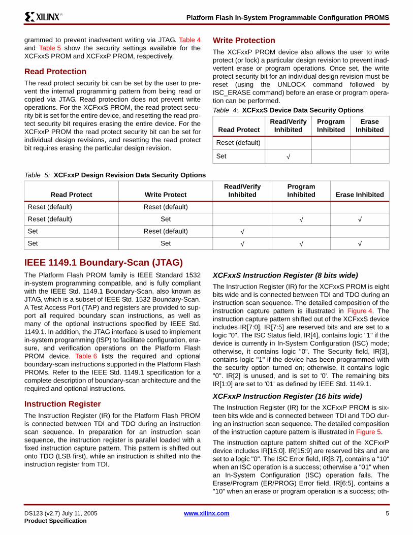
Platform Flash In-System Programmable Configuration PROMS
DS123 (v27) July 11 2005 wwwxilinxcom 5Product Specification
R
grammed to prevent inadvertent writing via JTAG Table 4and Table 5 show the security settings available for theXCFxxS PROM and XCFxxP PROM respectively
Read ProtectionThe read protect security bit can be set by the user to pre-vent the internal programming pattern from being read orcopied via JTAG Read protection does not prevent writeoperations For the XCFxxS PROM the read protect secu-rity bit is set for the entire device and resetting the read pro-tect security bit requires erasing the entire device For theXCFxxP PROM the read protect security bit can be set forindividual design revisions and resetting the read protectbit requires erasing the particular design revision
Write ProtectionThe XCFxxP PROM device also allows the user to writeprotect (or lock) a particular design revision to prevent inad-vertent erase or program operations Once set the writeprotect security bit for an individual design revision must bereset (using the UNLOCK command followed byISC_ERASE command) before an erase or program opera-tion can be performed
IEEE 11491 Boundary-Scan (JTAG)The Platform Flash PROM family is IEEE Standard 1532in-system programming compatible and is fully compliantwith the IEEE Std 11491 Boundary-Scan also known asJTAG which is a subset of IEEE Std 1532 Boundary-ScanA Test Access Port (TAP) and registers are provided to sup-port all required boundary scan instructions as well asmany of the optional instructions specified by IEEE Std11491 In addition the JTAG interface is used to implementin-system programming (ISP) to facilitate configuration era-sure and verification operations on the Platform FlashPROM device Table 6 lists the required and optionalboundary-scan instructions supported in the Platform FlashPROMs Refer to the IEEE Std 11491 specification for acomplete description of boundary-scan architecture and therequired and optional instructions
Instruction RegisterThe Instruction Register (IR) for the Platform Flash PROMis connected between TDI and TDO during an instructionscan sequence In preparation for an instruction scansequence the instruction register is parallel loaded with afixed instruction capture pattern This pattern is shifted outonto TDO (LSB first) while an instruction is shifted into theinstruction register from TDI
XCFxxS Instruction Register (8 bits wide)The Instruction Register (IR) for the XCFxxS PROM is eightbits wide and is connected between TDI and TDO during aninstruction scan sequence The detailed composition of theinstruction capture pattern is illustrated in Figure 4 Theinstruction capture pattern shifted out of the XCFxxS deviceincludes IR[70] IR[75] are reserved bits and are set to alogic 0 The ISC Status field IR[4] contains logic 1 if thedevice is currently in In-System Configuration (ISC) modeotherwise it contains logic 0 The Security field IR[3]contains logic 1 if the device has been programmed withthe security option turned on otherwise it contains logic0 IR[2] is unused and is set to 0 The remaining bitsIR[10] are set to 01 as defined by IEEE Std 11491
XCFxxP Instruction Register (16 bits wide)The Instruction Register (IR) for the XCFxxP PROM is six-teen bits wide and is connected between TDI and TDO dur-ing an instruction scan sequence The detailed compositionof the instruction capture pattern is illustrated in Figure 5The instruction capture pattern shifted out of the XCFxxPdevice includes IR[150] IR[159] are reserved bits and areset to a logic 0 The ISC Error field IR[87] contains a 10when an ISC operation is a success otherwise a 01 whenan In-System Configuration (ISC) operation fails TheEraseProgram (ERPROG) Error field IR[65] contains a10 when an erase or program operation is a success oth-
Table 4 XCFxxS Device Data Security Options
Read ProtectReadVerify
InhibitedProgram Inhibited
Erase Inhibited
Reset (default)
Set radic
Table 5 XCFxxP Design Revision Data Security Options
Read Protect Write ProtectReadVerify
InhibitedProgram Inhibited Erase Inhibited
Reset (default) Reset (default)
Reset (default) Set radic radic
Set Reset (default) radic
Set Set radic radic radic
Platform Flash In-System Programmable Configuration PROMS
DS123 (v27) July 11 2005 wwwxilinxcom 6Product Specification
R
erwise a 01 when an erase or program operation fails TheEraseProgram (ERPROG) Status field IR[4] contains alogic 1 when the device is busy performing an erase orprogramming operation otherwise it contains a logic 0The ISC Status field IR[3] contains logic 1 if the device iscurrently in In-System Configuration (ISC) mode otherwise
it contains logic 0 The DONE field IR[2] contains logic1 if the sampled design revision has been successfullyprogrammed otherwise a logic 0 indicates incompleteprogramming The remaining bits IR[10] are set to 01 asdefined by IEEE Std 11491
Boundary Scan RegisterThe boundary-scan register is used to control and observethe state of the device pins during the EXTEST SAM-PLEPRELOAD and CLAMP instructions Each output pinon the Platform Flash PROM has two register stages whichcontribute to the boundary-scan register while each inputpin has only one register stage The bidirectional pins havea total of three register stages which contribute to theboundary-scan register For each output pin the register
stage nearest to TDI controls and observes the output stateand the second stage closest to TDO controls and observesthe High-Z enable state of the output pin For each input pina single register stage controls and observes the input stateof the pin The bidirectional pin combines the three bits theinput stage bit is first followed by the output stage bit andfinally the output enable stage bit The output enable stagebit is closest to TDO
Table 6 Platform Flash PROM Boundary Scan Instructions
Boundary-Scan CommandXCFxxS IR[70]
(hex)XCFxxP IR[150]
(hex) Instruction Description
Required Instructions
BYPASS FF FFFF Enables BYPASS
SAMPLEPRELOAD 01 0001 Enables boundary-scan SAMPLEPRELOAD operation
EXTEST 00 0000 Enables boundary-scan EXTEST operation
Optional Instructions
CLAMP FA 00FA Enables boundary-scan CLAMP operation
HIGHZ FC 00FCPlaces all outputs in high-impedance state simultaneously
IDCODE FE 00FE Enables shifting out 32-bit IDCODE
USERCODE FD 00FD Enables shifting out 32-bit USERCODE
Platform Flash PROM Specific Instructions
CONFIG EE 00EE
Initiates FPGA configuration by pulsing CF pin Low once (For the XCFxxP this command also resets the selected design revision based on either the external REV_SEL[10] pins or on the internal design revision selection bits)(1)
Notes 1 For more information see Initiating FPGA Configuration
TDI rarr IR[75] IR[4] IR[3] IR[2] IR[10]
rarr TDOReserved ISC Status Security 0 0 1
Figure 4 XCFxxS Instruction Capture Values Loaded into IR as part of an Instruction Scan Sequence
TDI rarr IR[159] IR[87] IR[65] IR[4] IR[3] IR[2] IR[10]
rarr TDOReserved ISC Error ERPROG
ErrorERPROG
Status ISC Status DONE 0 1
Figure 5 XCFxxP Instruction Capture Values Loaded into IR as part of an Instruction Scan Sequence
Platform Flash In-System Programmable Configuration PROMS
DS123 (v27) July 11 2005 wwwxilinxcom 7Product Specification
R
See the XCFxxSXCFxxP Pin Names and DescriptionsTables in the Pinouts and Pin Descriptions section for theboundary-scan bit order for all connected device pins orsee the appropriate BSDL file for the complete bound-ary-scan bit order description under the attributeBOUNDARY_REGISTER section in the BSDL file The bitassigned to boundary-scan cell 0 is the LSB in the bound-ary-scan register and is the register bit closest to TDO
Identification RegistersIDCODE RegisterThe IDCODE is a fixed vendor-assigned value that is usedto electrically identify the manufacturer and type of thedevice being addressed The IDCODE register is 32 bitswide The IDCODE register can be shifted out for examina-tion by using the IDCODE instruction The IDCODE is avail-able to any other system component via JTAG Table 7 liststhe IDCODE register values for the Platform Flash PROMsThe IDCODE register has the following binary format
vvvvffffffffaaaaaaaaccccccccccc1
wherev = the die version numberf = the PROM family codea = the specific Platform Flash PROM product IDc = the Xilinx manufacturers IDThe LSB of the IDCODE register is always read as logic 1as defined by IEEE Std 11491
USERCODE RegisterThe USERCODE instruction gives access to a 32-bit userprogrammable scratch pad typically used to supply informa-tion about the devices programmed contents By using theUSERCODE instruction a user-programmable identifica-tion code can be shifted out for examination This code isloaded into the USERCODE register during programming ofthe Platform Flash PROM If the device is blank or was notloaded during programming the USERCODE register con-tains FFFFFFFFh
Customer Code RegisterFor the XCFxxP Platform Flash PROM in addition to theUSERCODE a unique 32-byte Customer Code can beassigned to each design revision enabled for the PROMThe Customer Code is set during programming and is typ-ically used to supply information about the design revisioncontents A private JTAG instruction is required to read theCustomer Code If the PROM is blank or the CustomerCode for the selected design revision was not loaded duringprogramming or if the particular design revision is erasedthe Customer Code will contain all ones
Platform Flash PROM TAP CharacteristicsThe Platform Flash PROM family performs both in-systemprogramming and IEEE 11491 boundary-scan (JTAG) test-ing via a single 4-wire Test Access Port (TAP) This simpli-fies system designs and allows standard Automatic TestEquipment to perform both functions The AC characteris-tics of the Platform Flash PROM TAP are described as fol-lows
TAP TimingFigure 6 shows the timing relationships of the TAP signalsThese TAP timing characteristics are identical for bothboundary-scan and ISP operations
Table 7 IDCODES Assigned to Platform Flash PROMsDevice IDCODE(1) (hex)
XCF01S ltvgt5044093
XCF02S ltvgt5045093
XCF04S ltvgt5046093
XCF08P ltvgt5057093
XCF16P ltvgt5058093
XCF32P ltvgt5059093
Notes 1 The ltvgt in the IDCODE field represents the devicersquos revision
code (in hex) and may vary
huffman
XCF08P ltvgt5057093
Platform Flash In-System Programmable Configuration PROMS
DS123 (v27) July 11 2005 wwwxilinxcom 8Product Specification
R
TAP AC ParametersTable 8 shows the timing parameters for the TAP waveforms shown in Figure 6
Additional Features for the XCFxxPInternal OscillatorThe 81632 Mbit XCFxxP Platform Flash PROMs includean optional internal oscillator which can be used to drive theCLKOUT and DATA pins on FPGA configuration interfaceThe internal oscillator can be enabled when programmingthe PROM and the oscillator can be set to either the defaultfrequency or to a slower frequency (AC CharacteristicsOver Operating Conditions When Cascading)
CLKOUTThe 81632 Mbit XCFxxP Platform Flash PROMs includethe programmable option to enable the CLKOUT signalwhich allows the PROM to provide a source synchronousclock aligned to the data on the configuration interface TheCLKOUT signal is derived from one of two clock sourcesthe CLK input pin or the internal oscillator The input clocksource is selected during the PROM programmingsequence Output data is available on the rising edge ofCLKOUT
The CLKOUT signal is enabled during programming and isactive when CE is Low and OERESET is High When dis-abled the CLKOUT pin is put into a high-impedance stateand should be pulled High externally to provide a knownstate When cascading Platform Flash PROMs with CLKOUTenabled after completing its data transfer the first PROMdisables CLKOUT and drives the CEO pin enabling the nextPROM in the PROM chain The next PROM will begin driv-ing the CLKOUT signal once that PROM is enabled anddata is available for transferDuring high-speed parallel configuration without compres-sion the FPGA drives the BUSY signal on the configurationinterface When BUSY is asserted High the PROMs inter-nal address counter stops incrementing and the currentdata value is held on the data outputs While BUSY is Highthe PROM will continue driving the CLKOUT signal to theFPGA clocking the FPGArsquos configuration logic When theFPGA deasserts BUSY indicating that it is ready to receiveadditional configuration data the PROM will begin drivingnew data onto the configuration interface
Figure 6 Test Access Port Timing
TCK
TCKMIN
TMSS
TMS
TDI
TDO
TMSH
TDIH
TDOV
TDIS
DS026_04_020300
Table 8 Test Access Port Timing ParametersSymbol Description Min Max Units
TCKMIN TCK minimum clock period when VCCJ = 25V or 33V 100 - ns
TMSS TMS setup time when VCCJ = 25V or 33V 10 - ns
TMSH TMS hold time when VCCJ = 25V or 33V 25 - ns
TDIS TDI setup time when VCCJ = 25V or 33V 10 - ns
TDIH TDI hold time when VCCJ = 25V or 33V 25 - ns
TDOV TDO valid delay when VCCJ = 25V or 33V - 30 ns
Platform Flash In-System Programmable Configuration PROMS
DS123 (v27) July 11 2005 wwwxilinxcom 9Product Specification
R
DecompressionThe 81632 Mbit XCFxxP Platform Flash PROMs include abuilt-in data decompressor compatible with Xilinx advancedcompression technology Compressed Platform FlashPROM files are created from the target FPGA bitstream(s)using the iMPACT software Only Slave Serial and SlaveSelectMAP (parallel) configuration modes are supported forFPGA configuration when using a XCFxxP PROM pro-grammed with a compressed bitstream Compression rateswill vary depending on several factors including the targetdevice family and the target design contentsThe decompression option is enabled during the PROMprogramming sequence The PROM decompresses thestored data before driving both clock and data onto theFPGAs configuration interface If Decompression isenabled then the Platform Flash clock output pin (CLK-
OUT) must be used as the clock signal for the configurationinterface driving the target FPGAs configuration clockinput pin (CCLK) Either the PROMs CLK input pin or theinternal oscillator must be selected as the source for CLK-OUT Any target FPGA connected to the PROM must oper-ate as slave in the configuration chain with theconfiguration mode set to Slave Serial mode or SlaveSelectMap (parallel) mode When decompression is enabled the CLKOUT signalbecomes a controlled clock output with a reduced maximumfrequency When decompressed data is not ready the CLK-OUT pin is put into a high-Z state and must be pulled Highexternally to provide a known stateThe BUSY input is automatically disabled when decom-pression is enabled
Design RevisioningDesign Revisioning allows the user to create up to fourunique design revisions on a single PROM or stored acrossmultiple cascaded PROMs Design Revisioning is sup-ported for the 81632 Mbit XCFxxP Platform Flash PROMsin both serial and parallel modes Design Revisioning canbe used with compressed PROM files and also when theCLKOUT feature is enabled The PROM programming filesalong with the revision information files (cfi) are createdusing the iMPACT software The cfi file is required toenable design revision programming in iMPACT A single design revision is composed of from 1 to n 8-Mbitmemory blocks If a single design revision contains lessthan 8 Mbits of data then the remaining space is paddedwith all ones A larger design revision can span several8-Mbit memory blocks and any space remaining in the last8-Mbit memory block is padded with all ones bull A single 32-Mbit PROM contains four 8-Mbit memory
blocks and can therefore store up to four separate design revisions one 32-Mbit design revision two 16-Mbit design revisions three 8-Mbit design revisions four 8-Mbit design revisions and so on
bull Because of the 8-Mbit minimum size requirement for each revision a single 16-Mbit PROM can only store up to two separate design revisions one 16-Mbit design revision one 8-Mbit design revision or two 8-Mbit design revisions
bull A single 8-Mbit PROM can store only one 8-Mbit design revision
Larger design revisions can be split over several cascadedPROMs For example two 32-Mbit PROMs can store up tofour separate design revisions one 64-Mbit design revisiontwo 32-Mbit design revisions three 16-Mbit design revi-sions four 16-Mbit design revisions and so on When cas-
cading one 16-Mbit PROM and one 8-Mbit PROM there are24 Mbits of available space and therefore up to three sepa-rate design revisions can be stored one 24-Mbit designrevision two 8-Mbit design revisions or three 8-Mbit designrevisions See Figure 7 for a few basic examples of how multiple revi-sions can be stored The design revision partitioning is han-dled automatically during file generation in iMPACT During the PROM file creation each design revision isassigned a revision number
Revision 0 = 00 Revision 1 = 01Revision 2 = 10Revision 3 = 11
After programming the Platform Flash PROM with a set ofdesign revisions a particular design revision can beselected using the external REV_SEL[10] pins or using theinternal programmable design revision control bits TheEN_EXT_SEL pin determines if the external pins or internalbits are used to select the design revision WhenEN_EXT_SEL is Low design revision selection is controlledby the external Revision Select pins REV_SEL[10] WhenEN_EXT_SEL is High design revision selection is con-trolled by the internal programmable Revision Select controlbits During power up the design revision selection inputs(pins or control bits) are sampled internally After power upwhen CE is asserted (Low) enabling the PROM inputs thedesign revision selection inputs are sampled again after therising edge of the CF pulse The data from the selecteddesign revision is then presented on the FPGA configura-tion interface
Platform Flash In-System Programmable Configuration PROMS
DS123 (v27) July 11 2005 wwwxilinxcom 10Product Specification
R
PROM to FPGA Configuration Mode and Connections SummaryThe FPGAs IO logical functions and internal interconnec-tions are established by the configuration data contained inthe FPGArsquos bitstream The bitstream is loaded into theFPGA either automatically upon power up or on commanddepending on the state of the FPGAs mode pins XilinxPlatform Flash PROMs are designed to download directly tothe FPGA configuration interface FPGA configurationmodes which are supported by the XCFxxS Platform FlashPROMs include Master Serial and Slave Serial FPGA con-figuration modes which are supported by the XCFxxP Plat-form Flash PROMs include Master Serial Slave SerialMaster SelectMAP and Slave SelectMAP Below is a shortsummary of the supported FPGA configuration modes Seethe respective FPGA data sheet for device configurationdetails including which configuration modes are supportedby the targeted FPGA device
FPGA Master Serial ModeIn Master Serial mode the FPGA automatically loads theconfiguration bitstream in bit-serial form from external mem-ory synchronized by the configuration clock (CCLK) gener-ated by the FPGA Upon power-up or reconfiguration theFPGAs mode select pins are used to select the MasterSerial configuration mode Master Serial Mode provides asimple configuration interface Only a serial data line aclock line and two control lines (INIT and DONE) arerequired to configure an FPGA Data from the PROM isread out sequentially on a single data line (DIN) accessedvia the PROMs internal address counter which is incre-mented on every valid rising edge of CCLK The serial bit-stream data must be set up at the FPGArsquos DIN input pin ashort time before each rising edge of the FPGAs internallygenerated CCLK signal
Figure 7 Design Revision Storage Examples
REV 0(8 Mbits)
REV 1(8 Mbits)
REV 2(8 Mbits)
REV 3(8 Mbits)
REV 0(8 Mbits)
REV 1(8 Mbits)
REV 2(16 Mbits)
REV 0(16 Mbits)
REV 1(16 Mbits)
REV 0(8 Mbits)
REV 1(24 Mbits)
REV 0(32 Mbits)
4 Design Revisions 3 Design Revisions 2 Design Revisions 1 Design Revision
(a) Design Revision storage examples for a single XCF32P PROM
REV 0(16 Mbits)
REV 1(16 Mbits)
REV 2(16 Mbits)
REV 3(16 Mbits)
REV 0(16 Mbits)
REV 1(16 Mbits)
REV 2(32 Mbits)
REV 0(32 Mbits)
REV 1(32 Mbits)
REV 0(16 Mbits)
REV 1(16 Mbits)
REV 0(32 Mbits)
4 Design Revisions 3 Design Revisions 2 Design Revisions 1 Design Revision
(b) Design Revision storage examples spanning two XCF32P PROMs
PROM 0 PROM 0 PROM 0 PROM 0 PROM 0
PROM 0 PROM 0 PROM 0 PROM 0 PROM 0
REV 0(32 Mbits)
REV 1(32 Mbits)
PROM 1 PROM 1 PROM 1 PROM 1 PROM 1
ds123_20_102103
Platform Flash In-System Programmable Configuration PROMS
DS123 (v27) July 11 2005 wwwxilinxcom 11Product Specification
R
Typically a wide range of frequencies can be selected forthe FPGArsquos internally generated CCLK which always startsat a slow default frequency The FPGArsquos bitstream containsconfiguration bits which can switch CCLK to a higher fre-quency for the remainder of the Master Serial configurationsequence The desired CCLK frequency is selected duringbitstream generationConnecting the FPGA device to the configuration PROM forMaster Serial Configuration Mode (Figure 8)bull The DATA output of the PROM(s) drive the DIN input of
the lead FPGA devicebull The Master FPGA CCLK output drives the CLK input(s)
of the PROM(s) bull The CEO output of a PROM drives the CE input of the
next PROM in a daisy chain (if any)bull The OERESET pins of all PROMs are connected to
the INIT_B pins of all FPGA devices This connection assures that the PROM address counter is reset before the start of any (re)configuration
bull The PROM CE input can be driven from the DONE pin The CE input of the first (or only) PROM can be driven by the DONE output of all target FPGA devices provided that DONE is not permanently grounded CE can also be permanently tied Low but this keeps the DATA output active and causes an unnecessary ICC active supply current (DC Characteristics Over Operating Conditions)
bull The PROM CF pin is typically connected to the FPGAs PROG_B (or PROGRAM) input For the XCFxxP only the CF pin is a bidirectional pin If the XCFxxP CF pin is not connected to the FPGAs PROG_B (or PROGRAM) input then the pin should be tied High
FPGA Slave Serial ModeIn Slave Serial mode the FPGA loads the configuration bit-stream in bit-serial form from external memory synchro-nized by an externally supplied clock Upon power-up orreconfiguration the FPGAs mode select pins are used toselect the Slave Serial configuration mode Slave SerialMode provides a simple configuration interface Only aserial data line a clock line and two control lines (INIT andDONE) are required to configure an FPGA Data from thePROM is read out sequentially on a single data line (DIN)accessed via the PROMs internal address counter which isincremented on every valid rising edge of CCLK The serialbitstream data must be set up at the FPGArsquos DIN input pin ashort time before each rising edge of the externally providedCCLKConnecting the FPGA device to the configuration PROM forSlave Serial Configuration Mode (Figure 9)bull The DATA output of the PROM(s) drive the DIN input of
the lead FPGA devicebull The PROM CLKOUT (for XCFxxP only) or an external
clock source drives the FPGAs CCLK input
bull The CEO output of a PROM drives the CE input of the next PROM in a daisy chain (if any)
bull The OERESET pins of all PROMs are connected to the INIT_B (or INIT) pins of all FPGA devices This connection assures that the PROM address counter is reset before the start of any (re)configuration
bull The PROM CE input can be driven from the DONE pin The CE input of the first (or only) PROM can be driven by the DONE output of all target FPGA devices provided that DONE is not permanently grounded CE can also be permanently tied Low but this keeps the DATA output active and causes an unnecessary ICC active supply current (DC Characteristics Over Operating Conditions)
bull The PROM CF pin is typically connected to the FPGAs PROG_B (or PROGRAM) input For the XCFxxP only the CF pin is a bidirectional pin If the XCFxxP CF pin is not connected to the FPGAs PROG_B (or PROGRAM) input then the pin should be tied High
Serial Daisy ChainMultiple FPGAs can be daisy-chained for serial configura-tion from a single source After a particular FPGA has beenconfigured the data for the next device is routed internallyto the FPGArsquos DOUT pin Typically the data on the DOUTpin changes on the falling edge of CCLK although for somedevices the DOUT pin changes on the rising edge of CCLKConsult the respective device data sheets for detailed infor-mation on a particular FPGA device For clocking thedaisy-chained configuration either the first FPGA in thechain can be set to Master Serial generating the CCLKwith the remaining devices set to Slave Serial (Figure 10)or all the FPGA devices can be set to Slave Serial and anexternally generated clock can be used to drive the FPGAsconfiguration interface
FPGA Master SelectMAP (Parallel) Mode(1)
In Master SelectMAP mode byte-wide data is written intothe FPGA typically with a BUSY flag controlling the flow ofdata synchronized by the configuration clock (CCLK) gen-erated by the FPGA Upon power-up or reconfiguration theFPGAs mode select pins are used to select the MasterSelectMAP configuration mode The configuration interfacetypically requires a parallel data bus a clock line and twocontrol lines (INIT and DONE) In addition the FPGArsquos ChipSelect Write and BUSY pins must be correctly controlled toenable SelectMAP configuration The configuration data isread from the PROM byte by byte on pins [D0D7]accessed via the PROMs internal address counter which isincremented on every valid rising edge of CCLK The bit-stream data must be set up at the FPGArsquos [D0D7] input
1 The Master SelectMAP (Parallel) FPGA configuration mode is sup-ported only by the XCFxxP Platform Flash PROM This mode is not supported by the XCFxxS Platform Flash PROM
Platform Flash In-System Programmable Configuration PROMS
DS123 (v27) July 11 2005 wwwxilinxcom 12Product Specification
R
pins a short time before each rising edge of the FPGAsinternally generated CCLK signal If BUSY is asserted(High) by the FPGA the configuration data must be helduntil BUSY goes Low An external data source or externalpull-down resistors must be used to enable the FPGAsactive Low Chip Select (CS or CS_B) and Write (WRITE orRDWR_B) signals to enable the FPGAs SelectMAP config-uration process The Master SelectMAP configuration interface is clocked bythe FPGArsquos internal oscillator Typically a wide range of fre-quencies can be selected for the internally generated CCLKwhich always starts at a slow default frequency The FPGArsquosbitstream contains configuration bits which can switchCCLK to a higher frequency for the remainder of the MasterSelectMAP configuration sequence The desired CCLK fre-quency is selected during bitstream generationAfter configuration the pins of the SelectMAP port can beused as additional user IO Alternatively the port can beretained using the persist optionConnecting the FPGA device to the configuration PROM forMaster SelectMAP (Parallel) Configuration Mode(Figure 11)bull The DATA outputs of the PROM(s) drive the [D0D7]
input of the lead FPGA devicebull The Master FPGA CCLK output drives the CLK input(s)
of the PROM(s) bull The CEO output of a PROM drives the CE input of the
next PROM in a daisy chain (if any)bull The OERESET pins of all PROMs are connected to
the INIT_B pins of all FPGA devices This connection assures that the PROM address counter is reset before the start of any (re)configuration
bull The PROM CE input can be driven from the DONE pin The CE input of the first (or only) PROM can be driven by the DONE output of all target FPGA devices provided that DONE is not permanently grounded CE can also be permanently tied Low but this keeps the DATA output active and causes an unnecessary ICC active supply current (DC Characteristics Over Operating Conditions)
bull For high-frequency parallel configuration the BUSY pins of all PROMs are connected to the FPGAs BUSY output This connection assures that the next data transition for the PROM is delayed until the FPGA is ready for the next configuration data byte
bull The PROM CF pin is typically connected to the FPGAs PROG_B (or PROGRAM) input For the XCFxxP only the CF pin is a bidirectional pin If the XCFxxP CF pin is not connected to the FPGAs PROG_B (or PROGRAM) input then the pin should be tied High
FPGA Slave SelectMAP (Parallel) Mode(1)
In Slave SelectMAP mode byte-wide data is written into theFPGA typically with a BUSY flag controlling the flow of
data synchronized by an externally supplied configurationclock (CCLK) Upon power-up or reconfiguration theFPGAs mode select pins are used to select the SlaveSelectMAP configuration mode The configuration interfacetypically requires a parallel data bus a clock line and twocontrol lines (INIT and DONE) In addition the FPGArsquos ChipSelect Write and BUSY pins must be correctly controlled toenable SelectMAP configuration The configuration data isread from the PROM byte by byte on pins [D0D7]accessed via the PROMs internal address counter which isincremented on every valid rising edge of CCLK The bit-stream data must be set up at the FPGArsquos [D0D7] inputpins a short time before each rising edge of the providedCCLK If BUSY is asserted (High) by the FPGA the config-uration data must be held until BUSY goes Low An externaldata source or external pull-down resistors must be used toenable the FPGAs active Low Chip Select (CS or CS_B)and Write (WRITE or RDWR_B) signals to enable theFPGAs SelectMAP configuration process After configuration the pins of the SelectMAP port can beused as additional user IO Alternatively the port can beretained using the persist optionConnecting the FPGA device to the configuration PROM forSlave SelectMAP (Parallel) Configuration Mode(Figure 12)bull The DATA outputs of the PROM(s) drives the [D0D7]
inputs of the lead FPGA devicebull The PROM CLKOUT (for XCFxxP only) or an external
clock source drives the FPGAs CCLK inputbull The CEO output of a PROM drives the CE input of the
next PROM in a daisy chain (if any)bull The OERESET pins of all PROMs are connected to
the INIT_B pins of all FPGA devices This connection assures that the PROM address counter is reset before the start of any (re)configuration
bull The PROM CE input can be driven from the DONE pin The CE input of the first (or only) PROM can be driven by the DONE output of all target FPGA devices provided that DONE is not permanently grounded CE can also be permanently tied Low but this keeps the DATA output active and causes an unnecessary ICC active supply current (DC Characteristics Over Operating Conditions)
bull For high-frequency parallel configuration the BUSY pins of all PROMs are connected to the FPGAs BUSY output This connection assures that the next data transition for the PROM is delayed until the FPGA is ready for the next configuration data byte
bull The PROM CF pin is typically connected to the FPGAs
1 The Slave SelectMAP (Parallel) FPGA configuration mode is sup-ported only by the XCFxxP Platform Flash PROMsThis mode is not supported by the XCFxxS Platform Flash PROM
Platform Flash In-System Programmable Configuration PROMS
DS123 (v27) July 11 2005 wwwxilinxcom 13Product Specification
R
PROG_B (or PROGRAM) input For the XCFxxP only the CF pin is a bidirectional pin If the XCFxxP CF pin is not connected to the FPGAs PROG_B (or PROGRAM) input then the pin should be tied High
FPGA SelectMAP (Parallel) Device Chaining(1)
Multiple Virtex-II FPGAs can be configured using theSelectMAP mode and be made to start up simultaneouslyTo configure multiple devices in this way wire the individualCCLK DONE INIT Data ([D0D7]) Write (WRITE orRDWR_B) and BUSY pins of all the devices in parallel If alldevices are to be configured with the same bitstream read-back is not being used and the CCLK frequency selecteddoes not require the use of the BUSY signal the CS_B pinscan be connected to a common line so all of the devices areconfigured simultaneously (Figure 13)With additional control logic the individual devices can beloaded separately by asserting the CS_B pin of each devicein turn and then enabling the appropriate configuration dataThe PROM can also store the individual bitstreams for eachFPGA for SelectMAP configuration in separate design revi-sions When design revisioning is utilized additional controllogic can be used to select the appropriate bitstream byasserting the EN_EXT_SEL pin and using theREV_SEL[10] pins to select the required bitstream whileasserting the CS_B pin for the FPGA the bitstream is target-ing (Figure 14) For clocking the parallel configuration chain either the firstFPGA in the chain can be set to Master SelectMAP gener-ating the CCLK with the remaining devices set to SlaveSelectMAP or all the FPGA devices can be set to SlaveSelectMAP and an externally generated clock can be usedto drive the configuration interface Again the respectivedevice data sheets should be consulted for detailed infor-mation on a particular FPGA device including which config-uration modes are supported by the targeted FPGA device
Cascading Configuration PROMsWhen configuring multiple FPGAs in a serial daisy chainconfiguring multiple FPGAs in a SelectMAP parallel chainor configuring a single FPGA requiring a larger configura-tion bitstream cascaded PROMs provide additional mem-ory (Figure 10 Figure 13 Figure 14 and Figure 15)Multiple Platform Flash PROMs can be concatenated byusing the CEO output to drive the CE input of the down-stream device The clock signal and the data outputs of allPlatform Flash PROMs in the chain are interconnectedAfter the last data from the first PROM is read the firstPROM asserts its CEO output Low and drives its outputs to
a high-impedance state The second PROM recognizes theLow level on its CE input and immediately enables its out-putsAfter configuration is complete address counters of all cas-caded PROMs are reset if the PROM OERESET pin goesLow or CE goes HighWhen utilizing the advanced features for the XCFxxP Plat-form Flash PROM including the clock output (CLKOUT)option decompression option or design revisioning pro-gramming files which span cascaded PROM devices canonly be created for cascaded chains containing onlyXCFxxP PROMs If the advanced features are not usedthen cascaded PROM chains can contain both XCFxxP andXCFxxS PROMs
Initiating FPGA ConfigurationThe options for initiating FPGA configuration via the Plat-form Flash PROM include1 Automatic configuration on power up2 Applying an external PROG_B (or PROGRAM) pulse3 Applying the JTAG CONFIG instructionFollowing the FPGArsquos power-on sequence or the assertionof the PROG_B (or PROGRAM) pin the FPGArsquos configura-tion memory is cleared the configuration mode is selectedand the FPGA is ready to accept a new configuration bit-stream The FPGArsquos PROG_B pin can be controlled by anexternal source or alternatively the Platform Flash PROMsincorporate a CF pin that can be tied to the FPGArsquosPROG_B pin Executing the CONFIG instruction throughJTAG pulses the CF output Low once for 300-500 ns reset-ting the FPGA and initiating configuration The iMPACTsoftware can issue the JTAG CONFIG command to initiateFPGA configuration by setting the Load FPGA option When using the XCFxxP Platform Flash PROM with designrevisioning enabled the CF pin should always be con-nected to the PROG_B (or PROGRAM) pin on the FPGA toensure that the current design revision selection is sampledwhen the FPGA is reset The XCFxxP PROM samples thecurrent design revision selection from the externalREV_SEL pins or the internal programmable RevisionSelect bits on the rising edge of CF When the JTAG CON-FIG command is executed the XCFxxP will sample the newdesign revision before initiating the FPGA configurationsequence When using the XCFxxP Platform Flash PROMwithout design revisioning if the CF pin is not connected tothe FPGA PROG_B (or PROGRAM) pin then the XCFxxPCF pin should be tied High
1 The SelectMAP (Parallel) FPGA configuration modes are supported only by the XCFxxP Platform Flash PROMThese modes are not sup-ported by the XCFxxS Platform Flash PROM
Platform Flash In-System Programmable Configuration PROMS
DS123 (v27) July 11 2005 wwwxilinxcom 14Product Specification
R
Configuration PROM to FPGA Device Interface Connection Diagrams
Figure 8 Configuring in Master Serial Mode
Xilinx FPGAMaster Serial
DIN
CCLK
DONE
INIT_B
PROG_B
TDI
TMS
TCK
GND
MODE PINS(1)
DOUT
TDO
VCCJ VCCO VCCINT
DIN
CCLK
DONE
INIT_B
PROG_B
DIN
CCLK
DONE
INIT_B
PROG_B
47
kΩ
47
kΩ (1)
VCCO(2)
OPTIONALDaisy-chainedSlave FPGAs with differentconfigurations
OPTIONALSlave FPGAs with identicalconfigurations
TDI
TMS
TCK
TDO
Notes1 For Mode pin connections and DONE pin pullup value refer to the appropriate FPGA data sheet2 For compatible voltages refer to the appropriate data sheet3 For the XCFxxS the CF pin is an output pin For the XCFxxP the CF pin is a bidirectional pin
Platform Flash PROM
VCCINT
VCCO(2)
VCCJ(2)
TDI
TMS
TCK
GND
D0
CLK
CE
CEO
OERESET
CF(3)
TDO
ds123_11_100804
Platform Flash In-System Programmable Configuration PROMS
DS123 (v27) July 11 2005 wwwxilinxcom 15Product Specification
R
Figure 9 Configuring in Slave Serial Mode
Xilinx FPGASlave Serial
DIN
CCLK
DONE
INIT_B
PROG_B
TDI
TMS
TCK
GND
MODE PINS(1)
DOUT
TDO
VCCJ VCCO VCCINT
DIN
CCLK
DONE
INIT_B
PROG_B
DIN
CCLK
DONE
INIT_B
PROG_B
47
kΩ
47
kΩ (1)
VCCO(2)
OPTIONALDaisy-chainedSlave FPGAs with differentconfigurations
OPTIONALSlave FPGAs with identicalconfigurations
TDI
TMS
TCK
TDO
Notes1 For Mode pin connections and DONE pin pullup value refer to the appropriate FPGA data sheet2 For compatible voltages refer to the appropriate data sheet3 In Slave Serial mode the configuration interface can be clocked by an external oscillator or optionallymdashfor the XCFxxP Platform Flash PROM onlymdashthe CLKOUT signal can be used to drive the FPGAs configuration clock (CCLK) If the XCFxxP PROMs CLKOUT signal is used then it must be tied to a 47KΩ resistor pulled up to VCCO4 For the XCFxxS the CF pin is an output pin For the XCFxxP the CF pin is a bidirectional pin
Platform Flash PROM
VCCINT
VCCO(2)
VCCJ(2)
TDI
TMS
TCK
GND
D0
CLK(3)
CE
CEO
OERESET
CF(4)
TDO
ds123_12_070505
External (3)
Oscillator
Platform Flash In-System Programmable Configuration PROMS
DS123 (v27) July 11 2005 wwwxilinxcom 16Product Specification
R
Figure 10 Configuring Multiple Devices MasterSlave Serial Mode
Platform Flash PROM
First PROM(PROM 0)
VCCINT
VCCO(2)
VCCJ(2)
TDI
TMS
TCK
D0
CLK
CE
CEO
OERESET
CF(3)
TDO
Xilinx FPGAMaster Serial
DIN
CCLK
DONE
INIT_B
PROG_B
TDI
TMS
TCK
MODE PINS(1)
DOUT
TDO
VCCJ VCCO VCCINT
47
kΩ
47
kΩ (1)
VCCO(2)
TDI
TMS
TCK
TDO
Notes1 For Mode pin connections and DONE pin pullup value refer to the appropriate FPGA data sheet2 For compatible voltages refer to the appropriate data sheet3 For the XCFxxS the CF pin is an output pin For the XCFxxP the CF pin is a bidirectional pin
Xilinx FPGASlave Serial
DIN
CCLK
DONE
INIT_B
PROG_B
TDI
TMS
TCK
Platform Flash PROM
Cascaded PROM(PROM 1)
VCCINT
VCCO(2)
VCCJ(2)
TDI
TMS
TCK
D0
CLK
CE
CEO
OERESET
CF(3)
TDO
VCCJ VCCO VCCINT
MODE PINS(1)
TDO
ds123_13_100804
GND
GNDGND
GND
Platform Flash In-System Programmable Configuration PROMS
DS123 (v27) July 11 2005 wwwxilinxcom 17Product Specification
R
Figure 11 Configuring in Master SelectMAP Mode
XCFxxPPlatform Flash PROM
VCCINT
VCCO(2)
VCCJ(2)
TDI
TMS
TCK
GND
D[07]
CLK
CE
CEO
OERESET
CF(5)
BUSY(4)
TDO
Xilinx FPGAMaster SelectMAP
D[07]
CCLK
DONE
INIT_B
PROG_B
BUSY(4)
TDI
TMS
TCK
GND
MODE PINS(1)
RDWR_B
CS_B
TDO
VCCJ VCCO VCCINT
D[07]
CCLK
DONE
INIT_B
PROG_B
BUSY(4)
47
kΩ
47
kΩ (1)
VCCO(2)
OPTIONALSlave FPGAs with identicalconfigurations
TDI
TMS
TCK
TDO
Notes1 For Mode pin connections and DONE pin pullup value refer to the appropriate FPGA data sheet2 For compatible voltages refer to the appropriate data sheet3 CS_B (or CS) and RDWR_B (or WRITE) must be either driven Low or pulled down exernally One option is shown4 The BUSY pin is only available with the XCFxxP Platform Flash PROM and the connection is only required for high-frequency SelectMAP mode configuration For BUSY pin requirements refer to the appropriate FPGA data sheet5 For the XCFxxP the CF pin is a bidirectional pin
1KΩ
1KΩ
IO(3)
IO(3)
ds123_14_100804
Platform Flash In-System Programmable Configuration PROMS
DS123 (v27) July 11 2005 wwwxilinxcom 18Product Specification
R
Figure 12 Configuring in Slave SelectMAP Mode
XCFxxPPlatform Flash PROM
VCCINT
VCCO(2)
VCCJ(2)
TDI
TMS
TCK
GND
D[07]
CLK(5)
CE
CEO
OERESET
CF(6)
BUSY(4)
TDO
Xilinx FPGASlave SelectMAP
D[07]
CCLK
DONE
INIT_B
PROG_B
BUSY(4)
TDI
TMS
TCK
GND
MODE PINS(1)
RDWR_B
CS_B
TDO
VCCJ VCCO VCCINT
D[07]
CCLK
DONE
INIT_B
PROG_B
BUSY(4)
47
kΩ
47
kΩ (1)
VCCO(2)
OPTIONALSlave FPGAs with identicalconfigurations
TDI
TMS
TCK
TDO
Notes1 For Mode pin connections and DONE pin pullup value refer to the appropriate FPGA data sheet2 For compatible voltages refer to the appropriate data sheet3 CS_B (or CS) and RDWR_B (or WRITE) must be either driven Low or pulled down exernally One option is shown4 The BUSY pin is only available with the XCFxxP Platform Flash PROM and the connection is only required for high-frequency SelectMAP mode configuration For BUSY pin requirements refer to the appropriate FPGA data sheet5 In Slave SelectMAP mode the configuration interface can be clocked by an external oscillator or optionally the CLKOUT signal can be used to drive the FPGAs configuration clock (CCLK) If the XCFxxP PROMs CLKOUT signal is used then it must be tied to a 47KΩ resistor pulled up to VCCO6 For the XCFxxP the CF pin is a bidirectional pin
1KΩ
1KΩ
IO(3)
IO(3)
ds123_15_070505
External (5)
Oscillator
Platform Flash In-System Programmable Configuration PROMS
DS123 (v27) July 11 2005 wwwxilinxcom 19Product Specification
R
Figure 13 Configuring Multiple Devices with Identical Patterns in MasterSlave SelectMAP Mode
XCFxxPPlatform Flash PROM
First PROM(PROM 0)
VCCINT
VCCO(2)
VCCJ(2)
TDI
TMS
TCK
GND
D[07]
CLK
CE
CEO
OERESET
CF(5)
BUSY(4)
TDO
Xilinx FPGAMaster SelectMAP
D[07]
CCLK
DONE
INIT_B
PROG_B
BUSY(4)
TDI
TMS
TCK
GND
MODE PINS(1)
TDO
VCCJ VCCO VCCINT
47
kΩ
47
kΩ (1)
VCCO(2)
TDI
TMS
TCK
TDO
Notes1 For Mode pin connections and DONE pin pullup value refer to the appropriate FPGA data sheet2 For compatible voltages refer to the appropriate data sheet3 CS_B (or CS) and RDWR_B (or WRITE) must be either driven Low or pulled down exernally One option is shown4 The BUSY pin is only available with the XCFxxP Platform Flash PROM and the connection is only required for high-frequency SelectMAP mode configuration For BUSY pin requirements refer to the appropriate FPGA data sheet5 For the XCFxxP the CF pin is a bidirectional pin
Xilinx FPGASlave SelectMAP
D[07]
CCLK
DONE
INIT_B
PROG_B
BUSY(4)
TDI
TMS
TCK
GND
XCFxxPPlatform Flash PROM
Cascaded PROM(PROM 1)
VCCINT
VCCO(2)
VCCJ(2)
TDI
TMS
TCK
GND
D[07]
CLK
CE
CEO
OERESET
CF(5)
BUSY(4)
TDO
VCCJ VCCO VCCINT
MODE PINS(1)
TDO
ds123_16_100804
1KΩ1K
Ω
IO(3)
IO(3)
1KΩ1K
Ω
IO(3)
IO(3)RDWR_B
CS_B
RDWR_B
CS_B
Platform Flash In-System Programmable Configuration PROMS
DS123 (v27) July 11 2005 wwwxilinxcom 20Product Specification
R
Figure 14 Configuring Multiple Devices with Design Revisioning in Slave Serial Mode
XCFxxPPlatform Flash PROM
First PROM(PROM 0)
VCCINT
VCCO(2)
VCCJ(2)
TDI
TMS
TCK
EN_EXT_SEL
REV_SEL[10]
D0
CLK(3)
CE
CEO
OERESET
CF(4)
TDO
Xilinx FPGASlave Serial
DIN
CCLK
DONE
INIT_B
PROG_B
TDI
TMS
TCK
VCCJ VCCO VCCINT
47
kΩ
47
kΩ
(1)
VCCO(2)
TDI
TMS
TCK
TDO
1 For Mode pin connections and DONE pin pullup value refer to the appropriate FPGA data sheet
2 For compatible voltages refer to the appropriate data sheet3 In Slave Serial mode the configuration interface can be clocked by an external oscillator or optionally the CLKOUT signal can be used to drive the FPGAs configuration clock (CCLK) If the XCFxxP PROMs CLKOUT signal is used then it must be tied to a 47KΩ resistor pulled up to VCCO4 For the XCFxxP the CF pin is a bidirectional pin
XCFxxPPlatform Flash PROM
Cascaded PROM(PROM 1)
VCCINT
VCCO(2)
VCCJ(2)
TDI
TMS
TCK
EN_EXT_SEL
REV_SEL[10]
D0
CLK(3)
CE
CEO
OERESET
CF(4)
TDO
VCCJ VCCO VCCINT
ds123_17_070505
Design RevisionControl Logic
EN_EXT_SEL
REV_SEL[10]
DONE
CF PROG_B
Xilinx FPGASlave Serial
DIN
CCLK
DONE
INIT_B
PROG_B
TDI
TMS
TCK
MODE PINS(1)
TDO
GNDGND
GND
DOUT
MODE PINS(1)
GND
External (3)
Oscillator
Platform Flash In-System Programmable Configuration PROMS
DS123 (v27) July 11 2005 wwwxilinxcom 21Product Specification
R
Figure 15 Configuring Multiple Devices with Design Revisioning in Slave SelectMAP Mode
XCFxxPPlatform Flash PROM
First PROM(PROM 0)
VCCINT
VCCO(2)
VCCJ(2)
TDI
TMS
TCK
EN_EXT_SEL
REV_SEL[10]
GND
D[07]
CLK(5)
CE
CEO
OERESET
CF(6)
BUSY(4)
TDO
Xilinx FPGASlave SelectMAP
D[07]
CCLK
DONE
INIT_B
PROG_B
BUSY(4)
TDI
TMS
TCK
MODE PINS(1)
RDWR_B
CS_B
TDO
VCCJ VCCO VCCINT
47
kΩ
47
kΩ
(1)
VCCO(2)
TDI
TMS
TCK
TDO
Notes
1 For Mode pin connections and DONE pin pullup value refer to the appropriate FPGA data sheet
2 For compatible voltages refer to the appropriate data sheet
3 RDWR_B (or WRITE) must be either driven Low or pulled down exernally One option is shown
4 The BUSY pin is only available with the XCFxxP Platform Flash PROM and the connection is only required for high frequency SelectMAP mode configuration For BUSY pin requirements refer to the appropriate FPGA data sheet
5 In Slave SelectMAP mode the configuration interface can be clocked by an external oscillator or optionally the CLKOUT signal can be used to drive the FPGAs configuration clock (CCLK) If the XCFxxP PROMs CLKOUT signal is used then it must be tied to a 47KΩ resistor pulled up to VCCO6 For the XCFxxP the CF pin is a bidirectional pin
Xilinx FPGASlave SelectMAP
D[07]
CCLK
DONE
INIT_B
PROG_B
BUSY(4)
TDI
TMS
TCK
MODE PINS(1)
RDWR_B
CS_B
TDO
XCFxxPPlatform Flash PROM
Cascaded PROM(PROM 1)
VCCINT
VCCO(2)
VCCJ(2)
TDI
TMS
TCK
EN_EXT_SEL
REV_SEL[10]
GND
D[07]
CLK(5)
CE
CEO
OERESET
CF(6)
BUSY(4)
TDO
VCCJ VCCO VCCINT
1KΩ
IO(3)
1KΩ
IO(3)
EN_EXT_SEL
REV_SEL[10]
CF
DONE
PROG_B
CS_B[10]
Design
Revision
Control
Logic
GND GND
ds123_18_070505
External (5)
Oscillator
Platform Flash In-System Programmable Configuration PROMS
DS123 (v27) July 11 2005 wwwxilinxcom 22Product Specification
R
Reset and Power-On Reset ActivationAt power up the device requires the VCCINT power supplyto monotonically rise to the nominal operating voltage withinthe specified VCCINT rise time If the power supply cannotmeet this requirement then the device might not performpower-on reset properly During the power-up sequenceOERESET is held Low by the PROM Once the requiredsupplies have reached their respective POR (Power OnReset) thresholds the OERESET release is delayed (TOERminimum) to allow more margin for the power supplies tostabilize before initiating configuration The OERESET pinis connected to an external 47kΩ pull-up resistor and alsoto the target FPGAs INIT pin For systems utilizing slow-ris-ing power supplies an additional power monitoring circuitcan be used to delay the target configuration until the sys-tem power reaches minimum operating voltages by holdingthe OERESET pin Low When OERESET is released theFPGArsquos INIT pin is pulled High allowing the FPGAs config-uration sequence to begin If the power drops below the
power-down threshold (VCCPD) the PROM resets andOERESET is again held Low until the after the POR thresh-old is reached OERESET polarity is not programmableThese power-up requirements are shown graphically inFigure 16For a fully powered Platform Flash PROM a reset occurswhenever OERESET is asserted (Low) or CE is deas-serted (High) The address counter is reset CEO is drivenHigh and the remaining outputs are placed in a high-imped-ance stateNotes1 The XCFxxS PROM only requires VCCINT to rise above
its POR threshold before releasing OERESET 2 The XCFxxP PROM requires both VCCINT to rise above
its POR threshold and for VCCO to reach the recommended operating voltage level before releasing OERESET
IO Input Voltage Tolerance and Power Sequencing The IOs on each re-programmable Platform Flash PROMare fully 33V-tolerant This allows 3V CMOS signals to con-nect directly to the inputs without damage The core powersupply (VCCINT) JTAG pin power supply (VCCJ) outputpower supply (VCCO) and external 3V CMOS IO signalscan be applied in any order Additionally for the XCFxxS PROM only when VCCO is sup-plied at 25V or 33V and VCCINT is supplied at 33V theIOs are 5V-tolerant This allows 5V CMOS signals to con-nect directly to the inputs on a powered XCFxxS PROMwithout damage Failure to power the PROM correctly whilesupplying a 5V input signal may result in damage to theXCFxxS device
Standby ModeThe PROM enters a low-power standby mode whenever CEis deasserted (High) In standby mode the address counteris reset CEO is driven High and the remaining outputs areplaced in a high-impedance state regardless of the state ofthe OERESET input For the device to remain in thelow-power standby mode the JTAG pins TMS TDI andTDO must not be pulled Low and TCK must be stopped(High or Low)When using the FPGA DONE signal to drive the PROM CEpin High to reduce standby power after configuration anexternal pull-up resistor should be used Typically a 330Ωpull-up resistor is used but refer to the appropriate FPGAdata sheet for the recommended DONE pin pull-up value Ifthe DONE circuit is connected to an LED to indicate FPGA
Figure 16 Platform Flash PROM Power-Up Requirements
TOER
VCCINT
VCCPOR
VCCPD
200 micros ramp50 ms ramp
TOER TRST
TIME (ms)
A slow-ramping VCCINT supply may still be below the minimum operating voltage when OERESET is released In this case the configuration sequence must be delayed until both VCCINT and VCCO have reached their recommended operating conditions
Recommended Operating Range
Delay or RestartConfiguration
ds123_21_103103
Platform Flash In-System Programmable Configuration PROMS
DS123 (v27) July 11 2005 wwwxilinxcom 23Product Specification
R
configuration is complete and is also connected to thePROM CE pin to enable low-power standby mode then anexternal buffer should be used to drive the LED circuit to
ensure valid transitions on the PROMrsquos CE pin If low-powerstandby mode is not required for the PROM then the CE pinshould be connected to ground
DC Electrical CharacteristicsThis data sheet is a Preliminary data sheet The DC characteristics are based on characterization rather than simulationFurther characteristic changes are not expected
bullAbsolute Maximum Ratings page 24bullSupply Voltage Requirements for Power-On Reset and Power-Down page 24bullRecommended Operating Conditions page 25bullQuality and Reliability Characteristics page 25bullDC Characteristics Over Operating Conditions page 26
Table 9 Truth Table for XCFxxS PROM Control InputsControl Inputs
Internal Address
Outputs
OERESET CE DATA CEO ICC
High LowIf address lt TC(2) increment Active High Active
If address = TC(2) dont change High-Z Low Reduced
Low Low Held reset High-Z High Active
X(1) High Held reset High-Z High Standby
Notes 1 X = donrsquot care2 TC = Terminal Count = highest address value TC + 1 = address 0
Table 10 Truth Table for XCFxxP PROM Control InputsControl Inputs
Internal Address
Outputs
OERESET CE CF BUSY(5) DATA CEO CLKOUT ICC
High Low High Low
If address lt TC(2) and address lt EA(3) increment Active High Active Active
If address lt TC(2) and address = EA(3) dont change High-Z High High-Z Reduced
Else If address = TC(2) dont change High-Z Low High-Z Reduced
High Low High High Unchanged Active and Unchanged High Active Active
High Low uarr X(1) Reset(4) Active High Active Active
Low Low X X Held reset(4) High-Z High High-Z Active
X High X X Held reset(4) High-Z High High-Z Standby
Notes 1 X = donrsquot care2 TC = Terminal Count = highest address value TC + 1 = address 03 For the XCFxxP with Design Revisioning enabled EA = end address (last address in the selected design revision) 4 For the XCFxxP with Design Revisioning enabled Reset = address reset to the beginning address of the selected bank If Design Revisioning is not
enabled then Reset = address reset to address 05 The BUSY input is only enabled when the XCFxxP is programmed for parallel data output and decompression is not enabled
Platform Flash In-System Programmable Configuration PROMS
DS123 (v27) July 11 2005 wwwxilinxcom 24Product Specification
R
AC Electrical CharacteristicsThis data sheet is a Preliminary data sheet The AC characteristics are based on characterization rather than simulationFurther characteristic changes are not expected
bullAC Characteristics Over Operating Conditions page 28bullAC Characteristics Over Operating Conditions When Cascading page 32
Absolute Maximum Ratings
Supply Voltage Requirements for Power-On Reset and Power-Down
Symbol DescriptionXCF01S XCF02S
XCF04SXCF08P XCF16P
XCF32P Units
VCCINT Internal supply voltage relative to GND ndash05 to +40 ndash05 to +27 V
VCCO IO supply voltage relative to GND ndash05 to +40 ndash05 to +40 V
VCCJ JTAG IO supply voltage relative to GND ndash05 to +40 ndash05 to +40 V
VIN Input voltage with respect to GNDVCCO lt 25V ndash05 to +36 ndash05 to +36 V
VCCO ge 25V ndash05 to +55 ndash05 to +36 V
VTS Voltage applied to High-Z outputVCCO lt 25V ndash05 to +36 ndash05 to +36 V
VCCO ge 25V ndash05 to +55 ndash05 to +36 V
TSTG Storage temperature (ambient) ndash65 to +150 ndash65 to +150 degC
TJ Junction temperature +125 +125 degC
Notes 1 Maximum DC undershoot below GND must be limited to either 05V or 10 mA whichever is easier to achieve During transitions the device pins can
undershoot to ndash20V or overshoot to +70V provided this over- or undershoot lasts less then 10 ns and with the forcing current being limited to 200 mA
2 Stresses beyond those listed under Absolute Maximum Ratings might cause permanent damage to the device These are stress ratings only and functional operation of the device at these or any other conditions beyond those listed under Operating Conditions is not implied Exposure to Absolute Maximum Ratings conditions for extended periods of time adversely affects device reliability
3 For soldering guidelines see the information on Packaging and Thermal Characteristics at wwwxilinxcom
Symbol Description
XCF01S XCF02S XCF04S
XCF08P XCF16P XCF32P
UnitsMin Max Min Max
TVCC VCCINT rise time from 0V to nominal voltage(2) 02 50 02 50 ms
VCCPOR POR threshold for the VCCINT supply 1 - 05 - V
TOER OERESET release delay following POR(3) 05 3 05 30 ms
VCCPD Power-down threshold for VCCINT supply - 1 - 05 V
TRSTTime required to trigger a device reset when the VCCINT supply drops below the maximum VCCPD threshold 10 - 10 - ms
Notes 1 VCCINT VCCO and VCCJ supplies may be applied in any order2 At power up the device requires the VCCINT power supply to monotonically rise to the nominal operating voltage within the specified TVCC rise time
If the power supply cannot meet this requirement then the device might not perform power-on-reset properly See Figure 16 page 223 If the VCCINT and VCCO supplies do not reach their respective recommended operating conditions before the OERESET pin is released then the
configuration data from the PROM will not be available at the recommended threshold levels The configuration sequence must be delayed until both VCCINT and VCCO have reached their recommended operating conditions
huffman
XCF08P
huffman
XCF08P
Platform Flash In-System Programmable Configuration PROMS
DS123 (v27) July 11 2005 wwwxilinxcom 25Product Specification
R
Recommended Operating Conditions
Quality and Reliability Characteristics
Symbol Description
XCF01S XCF02S XCF04S XCF08P XCF16P XCF32P
UnitsMin Typ Max Min Typ MaxVCCINT Internal voltage supply 30 33 36 165 18 20 V
VCCOSupply voltage for output drivers
33V Operation 30 33 36 30 33 36 V
25V Operation 23 25 27 23 25 27 V
18V Operation 17 18 19 17 18 19 V
15V Operation - - - TBD 15 TBD V
VCCJSupply voltage for JTAG output drivers
33V Operation 30 33 36 30 33 36 V
25V Operation 23 25 27 23 25 27 V
VILLow-level input voltage
33V Operation 0 - 08 0 - 08 V
25V Operation 0 - 08 0 - 08 V
18V Operation - - 20 VCCO - - 20 VCCO V
15V Operation - - - 0 - TBD V
VIHHigh-level input voltage
33V Operation 20 - 55 20 - 36 V
25V Operation 17 - 55 17 - 36 V
18V Operation 70 VCCO - 36 70 VCCO - 36 V
15V Operation - - - TBD - 36 V
TIN Input signal transition time(1) - - 500 - - 500 ns
VO Output voltage 0 - VCCO 0 - VCCO V
TA Operating ambient temperature ndash40 - 85 ndash40 - 85 degC
Notes 1 Input signal transition time measured between 10 VCCO and 90 VCCO
Symbol Description Min Max Units
TDR Data retention 20 - Years
NPE Programerase cycles (Endurance) 20000 - Cycles
VESD Electrostatic discharge (ESD) 2000 - Volts
huffman
XCF08P
huffman
18
Platform Flash In-System Programmable Configuration PROMS
DS123 (v27) July 11 2005 wwwxilinxcom 26Product Specification
R
DC Characteristics Over Operating Conditions
Symbol Description
XCF01S XCF02S XCF04S
XCF08P XCF16P XCF32P
UnitsTest
Conditions Min MaxTest
Conditions Min Max
VOH
High-level output voltage for 33V outputs IOH = ndash4 mA 24 - IOH = ndash4 mA 24 - V
High-level output voltage for 25V outputs IOH = ndash500 microA VCCO ndash 04
- IOH = ndash500 microA VCCO ndash 04
- V
High-level output voltage for 18V outputs IOH = ndash50 microA VCCO ndash 04
- IOH = ndash50 microA VCCO ndash 04
- V
High-level output voltage for 15V outputs - - - IOH = TBD TBD - V
VOL
Low-level output voltage for 33V outputs IOL = 4 mA - 04 IOL = 4 mA - 04 V
Low-level output voltage for 25V outputs IOL = 500 microA - 04 IOL = 500 microA - 04 V
Low-level output voltage for 18V outputs IOL = 50 microA - 04 IOL = 50 microA - 04 V
Low-level output voltage for 15V outputs - - - IOL = TBD - TBD V
ICCINT Internal voltage supply current active mode 33 MHz - 10 33 MHz - 10 mA
ICCO(1)
Output driver supply current active serial mode 33 MHz - 10 33 MHz - 10 mA
Output driver supply current active parallel mode - - - 33 MHz - 40 mA
ICCJ JTAG supply current active mode Note (2) - 5 Note (2) - 5 mA
ICCINTS Internal voltage supply current standby mode Note (3) - 5 Note (3) - 5 mA
ICCOS Output driver supply current standby mode Note (3) - 1 Note (3) - 1 mA
ICCJS JTAG supply current standby mode Note (3) - 1 Note (3) - 1 mA
IILJ JTAG pins TMS TDI and TDO pull-up current VCCJ = maxVIN = GND - 100 VCCJ = max
VIN = GND - 100 microA
IIL Input leakage current
VCCINT = maxVCCO = maxVIN = GND or
VCCO
ndash10 10
VCCINT = maxVCCO = maxVIN = GND or
VCCO
ndash10 10 microA
IIH Input and output High-Z leakage current
VCCINT = maxVCCO = maxVIN = GND or
VCCO
ndash10 10
VCCINT = maxVCCO = maxVIN = GND or
VCCO
ndash10 10 microA
IILPSource current through internal pull-ups onEN_EXT_SEL REV_SEL0 REV_SEL1
- - -
VCCINT = maxVCCO = maxVIN = GND or
VCCO
- 100 microA
IIHP Sink current through internal pull-down on BUSY - - -
VCCINT = maxVCCO = maxVIN = GND or
VCCO
-100 - microA
huffman
XCF08P
Platform Flash In-System Programmable Configuration PROMS
DS123 (v27) July 11 2005 wwwxilinxcom 27Product Specification
R
CIN Input capacitance VIN = GNDf = 10 MHz - 8 VIN = GND
f = 10 MHz - 8 pF
COUT Output capacitance VIN = GNDf = 10 MHz - 14 VIN = GND
f = 10 MHz - 14 pF
Notes 1 Output driver supply current specification based on no load conditions2 TDITMSTCK non-static (active)3 CE High OE Low and TMSTDITCK static
Symbol Description
XCF01S XCF02S XCF04S
XCF08P XCF16P XCF32P
UnitsTest
Conditions Min MaxTest
Conditions Min Max
huffman
XCF08P
Platform Flash In-System Programmable Configuration PROMS
DS123 (v27) July 11 2005 wwwxilinxcom 28Product Specification
R
AC Characteristics Over Operating Conditions
Symbol Description
XCF01S XCF02S XCF04S
XCF08P XCF16P XCF32P
UnitsMin Max Min Max
TOEOERESET to data delay(6) when VCCO = 33V or 25V - 10 - 25 ns
OERESET to data delay(6) when VCCO = 18V - 30 - 25 ns
TCECE to data delay(5) when VCCO = 33V or 25V - 15 - 25 ns
CE to data delay(5) when VCCO = 18V - 30 - 25 ns
TCACCLK to data delay(7) when VCCO = 33V or 25V - 15 - 25 ns
CLK to data delay(7) when VCCO = 18V - 30 - 25 ns
TOH
Data hold from CE OERESET or CLKwhen VCCO = 33V or 25V 0 - 5 - ns
Data hold from CE OERESET or CLKwhen VCCO = 18V 0 - 5 - ns
TDF
CE or OERESET to data float delay(2)
when VCCO = 33V or 25V - 25 - 45 ns
CE or OERESET to data float delay(2)
when VCCO = 18V - 30 - 45 ns
TCYC
Clock period(7) (serial mode) when VCCO = 33V or 25V 30 - 25 - ns
Clock period(7) (serial mode) when VCCO = 18V 67 - 25 - ns
Clock period(7) (parallel mode) when VCCO = 33V or 25V - - 30 - ns
Clock period(7) (parallel mode) when VCCO = 18V - - 30 - ns
CE
OERESET
CLK
CLKOUT(optional)
BUSY(optional)
DATA
TCE
TLC THC
TSCE
TOE TCAC
THCE
THOE
TCYC
TOH
TDFTOH
THBTSBTOEC
TCEC
TCLKO
TCOH
TCDD
CF
EN_EXT_SEL
REV_SEL[10]
TSXT THXT
TSRV THRV
ds123_22_110403
huffman
XCF08P
Platform Flash In-System Programmable Configuration PROMS
DS123 (v27) July 11 2005 wwwxilinxcom 29Product Specification
R
TLCCLK Low time(3) when VCCO = 33V or 25V 10 - 12 - ns
CLK Low time(3) when VCCO = 18V 15 - 12 - ns
THCCLK High time(3) when VCCO = 33V or 25V 10 - 12 - ns
CLK High time(3) when VCCO = 18V 15 - 12 - ns
TSCE
CE setup time to CLK (guarantees proper counting)(3)
when VCCO = 33V or 25V 20 - 30 - ns
CE setup time to CLK (guarantees proper counting)(3)
when VCCO = 18V 30 30 - ns
THCE
CE hold time (guarantees counters are reset)(5)
when VCCO = 33V or 25V 250 - 2000 - ns
CE hold time (guarantees counters are reset)(5)
when VCCO = 18V 250 - 2000 - ns
THOE
OERESET hold time (guarantees counters are reset)(6)
when VCCO = 33V or 25V 250 - 2000 - ns
OERESET hold time (guarantees counters are reset)(6)
when VCCO = 18V 250 - 2000 - ns
TSBBUSY setup time to CLK when VCCO = 33V or 25V - - 12 - ns
BUSY setup time to CLK when VCCO = 18V - - 12 - ns
THBBUSY hold time to CLK when VCCO = 33V or 25V - - 8 - ns
BUSY hold time to CLK when VCCO = 18V - - 8 - ns
TCLKO
CLK input to CLKOUT output delay when VCCO = 33V or 25V - - - 35 ns
CLK input to CLKOUT output delay when VCCO = 18V - - - 35 ns
CLK input to CLKOUT output delay when VCCO = 33V or 25V with decompression(12) - - - 35 ns
CLK input to CLKOUT output delay when VCCO = 18V with decompression(12) - - - 35 ns
TCEC
CE to CLKOUT delay(8) with CLKOUT sourced from internal oscillator when VCCO = 33V or 25V - - 0 1 micros
CE to CLKOUT delay(8) with CLKOUT sourced from internal oscillator when VCCO = 18V - - 0 1 micros
CE to CLKOUT delay(8) with CLKOUT sourced from external CLK input when VCCO = 33V or 25V - - 0 2 CLK
cycles -
CE to CLKOUT delay(8) with CLKOUT sourced from external CLK input when VCCO = 18V - - 0 2 CLK
cycles -
TOEC
OERESET to CLKOUT delay(8) with CLKOUT sourced from internal oscillator when VCCO = 33V or 25V - - 0 1 micros
OERESET to CLKOUT delay(8) with CLKOUT sourced from internal oscillator when VCCO = 18V - - 0 1 micros
OERESET to CLKOUT delay(8) with CLKOUT sourced from external CLK input when VCCO = 33V or 25V 0 2 CLK
cycles -
OERESET to CLKOUT delay(8) with CLKOUT sourced from external CLK input when VCCO = 18V 0 2 CLK
cycles -
Symbol Description
XCF01S XCF02S XCF04S
XCF08P XCF16P XCF32P
UnitsMin Max Min Max
huffman
XCF08P
Platform Flash In-System Programmable Configuration PROMS
DS123 (v27) July 11 2005 wwwxilinxcom 30Product Specification
R
TCDDCLKOUT to data delay when VCCO = 33V or 25V(9) - - - 22 ns
CLKOUT to data delay when VCCO = 18V(9) - - - 22 ns
TDDC
Data setup time to CLKOUT when VCCO = 33V or 25V with decompression(9)(12) - - 5 ns
Data setup time to CLKOUT when VCCO = 18V with decompression(9)(12) - - 5 ns
TCOH
Data hold from CLKOUT when VCCO = 33V or 25V - - 3 - ns
Data hold from CLKOUT when VCCO = 18V - - 3 - ns
Data hold from CLKOUT when VCCO = 33V or 25V with decompression(12) - - 3 - ns
Data hold from CLKOUT when VCCO = 18V with decompression(12) - - 3 - ns
TSXT
EN_EXT_SEL setup time to CF (rising edge)when VCCO = 33V or 25V - - 300 - ns
EN_EXT_SEL setup time to CF (rising edge)when VCCO = 18V - - 300 - ns
THXT
EN_EXT_SEL hold time from CF (rising edge)when VCCO = 33V or 25V - - 300 - ns
EN_EXT_SEL hold time from CF (rising edge)when VCCO = 18V - - 300 - ns
TSRV
REV_SEL setup time to CF (rising edge)when VCCO = 33V or 25V - - 300 - ns
REV_SEL setup time to CF (rising edge)when VCCO = 18V - - 300 - ns
THRV
REV_SEL hold time from CF (rising edge)when VCCO = 33V or 25V - - 300 - ns
REV_SEL hold time from CF (rising edge)when VCCO = 18V - - 300 - ns
FF
CLKOUT default (fast) frequency(10) - - 25 50 MHz
CLKOUT default (fast) frequency with decompression(12) - - 125 25 MHz
Symbol Description
XCF01S XCF02S XCF04S
XCF08P XCF16P XCF32P
UnitsMin Max Min Max
huffman
XCF08P
Platform Flash In-System Programmable Configuration PROMS
DS123 (v27) July 11 2005 wwwxilinxcom 31Product Specification
R
FS
CLKOUT alternate (slower) frequency(11) - - 125 25 MHz
CLKOUT alternate (slower) frequency with decompression(12) - - 6 125 MHz
Notes 1 AC test load = 50 pF for XCF01SXCF02SXCF04S 30 pF for XCF08PXCF16PXCF32P2 Float delays are measured with 5 pF AC loads Transition is measured at plusmn200 mV from steady-state active levels3 Guaranteed by design not tested4 All AC parameters are measured with VIL = 00V and VIH = 30V5 If THCE High lt 2 micros TCE = 2 micros6 If THOE Low lt 2 micros TOE = 2 micros7 This is the minimum possible TCYC Actual TCYC = TCAC + FPGA Data setup time
Example With the XCF32P in serial mode with VCCO at 33V if FPGA Data setup time = 15 ns then the actual TCYC = 25 ns +15 ns = 40 ns8 The delay before the enabled CLKOUT signal begins clocking data out of the device is dependent on the clocking configuration The delay before
CLKOUT is enabled will increase if decompression is enabled 9 Slower CLK frequency option may be required to meet the FPGA data sheet setup time10 Typical CLKOUT default (fast) period = 25 ns (40 MHz)11 Typical CLKOUT alternate (slower) period = 50 ns (20 MHz)12 When decompression is enabled the CLKOUT signal becomes a controlled clock output When decompressed data is available CLKOUT will toggle
at frac12 the source clock frequency (either frac12 the selected internal clock frequency or frac12 the external CLK input frequency) When decompressed data is not available the CLKOUT pin is parked High If CLKOUT is used then it must be pulled High externally using a 47kΩ pull-up to VCCO
Symbol Description
XCF01S XCF02S XCF04S
XCF08P XCF16P XCF32P
UnitsMin Max Min Max
huffman
XCF08P
huffman
XCF08P
Platform Flash In-System Programmable Configuration PROMS
DS123 (v27) July 11 2005 wwwxilinxcom 32Product Specification
R
AC Characteristics Over Operating Conditions When Cascading
Symbol Description
XCF01S XCF02S XCF04S
XCF08P XCF16P XCF32P
UnitsMin Max Min Max
TCDF
CLK to output float delay(23) when VCCO = 25V or 33V - 25 - 20 ns
CLK to output float delay(23) when VCCO = 18V - 35 - 20 ns
TOCKCLK to CEO delay(35) when VCCO = 25V or 33V - 20 - 20 ns
CLK to CEO delay(35) when VCCO = 18V - 35 - 20 ns
TOCECE to CEO delay(36) when VCCO = 25V or 33V - 20 - 80 ns
CE to CEO delay(36) when VCCO = 18V - 35 - 80 ns
TOOEOERESET to CEO delay(3) when VCCO = 25V or 33V - 20 - 80 ns
OERESET to CEO delay(3) when VCCO = 18V - 35 - 80 ns
TCOCECLKOUT to CEO delay when VCCO = 25V or 33V - - - 20 ns
CLKOUT to CEO delay when VCCO = 18V - - - 20 ns
TCODF
CLKOUT to output float delay when VCCO = 25V or 33V - - - 25 ns
CLKOUT to output float delay when VCCO = 18V - - - 25 ns
Notes 1 AC test load = 50 pF for XCF01SXCF02SXCF04S 30 pF for XCF08PXCF16PXCF32P2 Float delays are measured with 5 pF AC loads Transition is measured at plusmn200 mV from steady state active levels3 Guaranteed by design not tested4 All AC parameters are measured with VIL = 00V and VIH = 30V5 For cascaded PROMs if the FPGArsquos dual-purpose configuration data pins are set to persist as configuration pins the minimum period is increased
based on the CLK to CEO and CE to data propagation delays- TCYC minimum = TOCK + TCE + FPGA Data setup time- TCAC maximum = TOCK + TCE
6 For cascaded PROMs if the FPGArsquos dual-purpose configuration data pins become general IO pins after configuration to allow for the disable to propagate to the cascaded PROMs and to avoid contention on the data lines following configuration the minimum period is increased based on the CE to CEO and CE to data propagation delays- TCYC minimum = TOCE + TCE - TCAC maximum = TOCK + TCE
OERESET
CE
CLK
CLKOUT(optional)
DATA
CEO
TOCETOOE
First BitLast Bit
TCDFTCODF
TOCK TCOCE
ds123_23_102203
huffman
XCF08P
huffman
XCF08P
Platform Flash In-System Programmable Configuration PROMS
DS123 (v27) July 11 2005 wwwxilinxcom 33Product Specification
R
Pinouts and Pin DescriptionsThe XCFxxS Platform Flash PROM is available in the VO20 and VOG20 packages The XCFxxP Platform Flash PROM isavailable in the VO48 VOG48 FS48 and FSG48 packages This section includes
bull Table 11 XCFxxS Pin Names and Descriptions page 33bull Figure 17 VO20VOG20 Pinout Diagram (Top View) with Pin Names page 34bull Table 12 XCFxxP Pin Names and Descriptions page 35bull Figure 18 VO48VOG48 Pinout Diagram (Top View) with Pin Names page 36bull Table 13 FS48FSG48 Pin NumberName Reference page 38bull Figure 19 FS48FSG48 Pinout Diagram (Top View) page 38
Notes 1 VO20VOG20 denotes a 20-pin (TSSOP) Plastic Thin Shrink Small Outline Package 2 VO48VOG48 denotes a 48-pin (TSOP) Plastic Thin Small Outline Package3 FS48FSG48 denotes a 48-pin (TFBGA) Plastic Thin Fine Pitch Ball Grid Array (08 mm pitch)
XCFxxS Pinouts and Pin DescriptionsTable 11 provides a list of the pin names and descriptions for the XCFxxS 20-pin VO20VOG20 package
Table 11 XCFxxS Pin Names and Descriptions
Pin NameBoundary
Scan OrderBoundary
Scan Function Pin Description20-pin TSSOP (VO20VOG20)
D04 Data Out D0 is the DATA output pin to provide data for configuring an
FPGA in serial mode The D0 output is set to a high-impedance state during ISPEN (when not clamped)
13 Output Enable
CLK 0 Data InConfiguration Clock Input Each rising edge on the CLK input increments the internal address counter if the CLK input is selected CE is Low and OERESET is High
3
OERESET
20 Data In Output EnableReset (Open-Drain IO) When Low this input holds the address counter reset and the DATA output is in a high-impedance state This is a bidirectional open-drain pin that is held Low while the PROM is reset Polarity is not programmable
819 Data Out
18 Output Enable
CE 15 Data InChip Enable Input When CE is High the device is put into low-power standby mode the address counter is reset and the DATA pins are put in a high-impedance state
10
CF22 Data Out Configuration Pulse (Open-Drain Output) Allows JTAG
CONFIG instruction to initiate FPGA configuration without powering down FPGA This is an open-drain output that is pulsed Low by the JTAG CONFIG command
721 Output Enable
CEO
12 Data OutChip Enable Output Chip Enable Output (CEO) is connected to the CE input of the next PROM in the chain This output is Low when CE is Low and OERESET input is High AND the internal address counter has been incremented beyond its Terminal Count (TC) value CEO returns to High when OERESET goes Low or CE goes High
13
11 Output Enable
TMS Mode Select
JTAG Mode Select Input The state of TMS on the rising edge of TCK determines the state transitions at the Test Access Port (TAP) controller TMS has an internal 50KΩ resistive pull-up to VCCJ to provide a logic 1 to the device if the pin is not driven
5
TCK ClockJTAG Clock Input This pin is the JTAG test clock It sequences the TAP controller and all the JTAG test and programming electronics
6
Platform Flash In-System Programmable Configuration PROMS
DS123 (v27) July 11 2005 wwwxilinxcom 34Product Specification
R
XCFxxS Pinout Diagram
TDI Data In
JTAG Serial Data Input This pin is the serial input to all JTAG instruction and data registers TDI has an internal 50KΩ resistive pull-up to VCCJ to provide a logic 1 to the device if the pin is not driven
4
TDO Data Out
JTAG Serial Data Output This pin is the serial output for all JTAG instruction and data registers TDO has an internal 50KΩ resistive pull-up to VCCJ to provide a logic 1 to the system if the pin is not driven
17
VCCINT +33V Supply Positive 33V supply voltage for internal logic 18
VCCO+33V 25V or 18V IO Supply Positive 33V 25V or 18V supply voltage connected to the output voltage drivers and input buffers
19
VCCJ+33V or 25V JTAG IO Supply Positive 33V 25V or 18V supply voltage connected to the TDO output voltage driver and TCK TMS and TDI input buffers
20
GND Ground 11
DNC Do not connect (These pins must be left unconnected) 2 9 12 14 15 16
Figure 17 VO20VOG20 Pinout Diagram (Top View) with Pin Names
Table 11 XCFxxS Pin Names and Descriptions (Continued)
Pin NameBoundary
Scan OrderBoundary
Scan Function Pin Description20-pin TSSOP (VO20VOG20)
VO20VOG20Top View
ds123_02_071304
1
2
3
4
5
6
7
8
9
10
20
19
18
17
16
15
14
13
12
11
D0
(DNC)
CLK
TDI
TMS
TCK
CF
OERESET
(DNC)
CE
VCCJ
VCCO
VCCINT
TDO
(DNC)
(DNC)
CEO
(DNC)
GND
(DNC)
Platform Flash In-System Programmable Configuration PROMS
DS123 (v27) July 11 2005 wwwxilinxcom 35Product Specification
R
XCFxxP Pinouts and Pin DescriptionsTable 12 provides a list of the pin names and descriptions for the XCFxxP 48-pin VO48VOG48 and 48-pin FS48FSG48packages
Table 12 XCFxxP Pin Names and Descriptions
Pin Name
Boundary Scan Order
Boundary Scan
Function Pin Description
48-pin TSOP (VO48VOG48)
48-pin TFBGA (FS48FSG48)
D028 Data Out
D0 is the DATA output pin to provide data for configuring an FPGA in serial mode D0-D7 are the DATA output pins to provide parallel data for configuring a Xilinx FPGA in SelectMap (parallel) mode The D0 output is set to a high-impedance state during ISPEN (when not clamped)The D1-D7 outputs are set to a high-impedance state during ISPEN (when not clamped) and when serial mode is selected for configuration The D1-D7 pins can be left unconnected when the PROM is used in serial mode
28 H627 Output Enable
D126 Data Out
29 H525 Output Enable
D224 Data Out
32 E523 Output Enable
D322 Data Out
33 D521 Output Enable
D420 Data Out
43 C519 Output Enable
D518 Data Out
44 B517 Output Enable
D616 Data Out
47 A515 Output Enable
D714 Data Out
48 A613 Output Enable
CLK 01 Data In
Configuration Clock Input An internal programmable control bit selects between the internal oscillator and the CLK input pin as the clock source to control the configuration sequence Each rising edge on the CLK input increments the internal address counter if the CLK input is selected CE is Low OERESET is High BUSY is Low (parallel mode only) and CF is High
12 B3
OERESET
04 Data In Output EnableReset (Open-Drain IO)When Low this input holds the address counter reset and the DATA and CLKOUT outputs are placed in a high-impedance state This is a bidirectional open-drain pin that is held Low while the PROM is reset Polarity is not programmable
11 A303 Data Out
02 Output Enable
CE 00 Data In
Chip Enable Input When CE is High the device is put into low-power standby mode the address counter is reset and the DATA and CLKOUT outputs are placed in a high-impedance state
13 B4
CF
11 Data InConfiguration Pulse (Open-Drain IO) As an output this pin allows the JTAG CONFIG instruction to initiate FPGA configuration without powering down the FPGA This is an open-drain signal that is pulsed Low by the JTAG CONFIG command As an input on the rising edge of CF the current design revision selection is sampled and the internal address counter is reset to the start address for the selected revision If unused the CF pin should be pulled High using an external 47KΩ pull-up to VCCO
6 D110 Data Out
09 Output Enable
Platform Flash In-System Programmable Configuration PROMS
DS123 (v27) July 11 2005 wwwxilinxcom 36Product Specification
R
CEO
06 Data OutChip Enable Output Chip Enable Output (CEO) is connected to the CE input of the next PROM in the chain This output is Low when CE is Low and OERESET input is High AND the internal address counter has been incremented beyond its Terminal Count (TC) value CEO returns to High when OERESET goes Low or CE goes High
10 D2
05 Output Enable
EN_EXT_SEL 31 Data In
Enable External Selection Input When this pin is Low design revision selection is controlled by the Revision Select pins When this pin is High design revision selection is controlled by the internal programmable Revision Select control bits EN_EXT_SEL has an internal 50KΩ resistive pull-up to VCCO to provide a logic 1 to the device if the pin is not driven
25 H4
REV_SEL0 30 Data InRevision Select[10] Inputs When the EN_EXT_SEL is Low the Revision Select pins are used to select the design revision to be enabled overriding the internal programmable Revision Select control bits The Revision Select[10] inputs have an internal 50KΩ resistive pull-up to VCCO to provide a logic 1 to the device if the pins are not driven
26 G3
REV_SEL1 29 Data In 27 G4
BUSY 12 Data In
Busy Input The BUSY input is enabled when parallel mode is selected for configuration When BUSY is High the internal address counter stops incrementing and the current data remains on the data pins On the first rising edge of CLK after BUSY transitions from High to Low the data for the next address is driven on the data pins When serial mode or decompression is enabled during device programming the BUSY input is disabled BUSY has an internal 50KΩ resistive pull-down to GND to provide a logic 0 to the device if the pin is not driven
5 C1
CLKOUT
08 Data Out
Configuration Clock Output An internal Programmable control bit enables the CLKOUT signal which is sourced from either the internal oscillator or the CLK input pin Each rising edge of the selected clock source increments the internal address counter if data is available CE is Low and OERESET is High Output data is available on the rising edge of CLKOUT CLKOUT is disabled if CE is High or OERESET is Low If decompression is enabled CLKOUT is parked High when decompressed data is not ready When CLKOUT is disabled the CLKOUT pin is put into a high-Z state If CLKOUT is used then it must be pulled High externally using a 47KΩ pull-up to VCCO
9 C2
07 Output Enable
TMS Mode Select
JTAG Mode Select Input The state of TMS on the rising edge of TCK determines the state transitions at the Test Access Port (TAP) controller TMS has an internal 50KΩ resistive pull-up to VCCJ to provide a logic 1 to the device if the pin is not driven
21 E2
TCK ClockJTAG Clock Input This pin is the JTAG test clock It sequences the TAP controller and all the JTAG test and programming electronics
20 H3
TDI Data In
JTAG Serial Data Input This pin is the serial input to all JTAG instruction and data registers TDI has an internal 50KΩ resistive pull-up to VCCJ to provide a logic 1 to the device if the pin is not driven
19 G1
Table 12 XCFxxP Pin Names and Descriptions (Continued)
Pin Name
Boundary Scan Order
Boundary Scan
Function Pin Description
48-pin TSOP (VO48VOG48)
48-pin TFBGA (FS48FSG48)
Platform Flash In-System Programmable Configuration PROMS
DS123 (v27) July 11 2005 wwwxilinxcom 37Product Specification
R
XCFxxP Pinout Diagrams
Figure 18 VO48VOG48 Pinout Diagram (Top View) with Pin Names
TDO Data Out
JTAG Serial Data Output This pin is the serial output for all JTAG instruction and data registers TDO has an internal 50KΩ resistive pull-up to VCCJ to provide a logic 1 to the system if the pin is not driven
22 E6
VCCINT +18V Supply Positive 18V supply voltage for internal logic 4 15 34
B1 E1 G6
VCCO+33V 25V or 18V IO Supply Positive 33V 25V or 18V supply voltage connected to the output voltage drivers and input buffers
8 30 38 45
B2 C6 D6 G5
VCCJ+33V or 25V JTAG IO Supply Positive 33V 25V or 18V supply voltage connected to the TDO output voltage driver and TCK TMS and TDI input buffers
24 H2
GND Ground2 7
17 23 31 36
46
A1 A2 B6 F1 F5 F6
H1
DNC Do Not Connect (These pins must be left unconnected)
1 3 14 16 18 35 37 39 40 41
42
A4 C3 C4 D3 D4 E3 E4 F2 F3 F4
G2
Table 12 XCFxxP Pin Names and Descriptions (Continued)
Pin Name
Boundary Scan Order
Boundary Scan
Function Pin Description
48-pin TSOP (VO48VOG48)
48-pin TFBGA (FS48FSG48)
123456789101112131415161718192021222324
484746454443424140393837363534333231302928272625
VO48VOG48Top View
DNCGNDDNC
VCCINTBUSY
CFGND
VCCOCLKOUT
CEOOERESET
CLKCE
DNCVCCINT
DNCGNDDNCTDI
TCKTMSTDOGND
D7D6GNDVCCOD5D4DNCDNCDNCDNCVCCODNCGNDDNCVCCINTD3D2GNDVCCOD1D0REV_SEL1REV_SEL0EN_EXT_SELVCCJ
Platform Flash In-System Programmable Configuration PROMS
DS123 (v27) July 11 2005 wwwxilinxcom 38Product Specification
R
Table 13 FS48FSG48 Pin NumberName ReferencePin
Number Pin NamePin
Number Pin NameA1 GND E1 VCCINT
A2 GND E2 TMS
A3 OERESET E3 DNC
A4 DNC E4 DNC
A5 D6 E5 D2
A6 D7 E6 TDO
B1 VCCINT F1 GND
B2 VCCO F2 DNC
B3 CLK F3 DNC
B4 CE F4 DNC
B5 D5 F5 GND
B6 GND F6 GND
C1 BUSY G1 TDI
C2 CLKOUT G2 DNC
C3 DNC G3 REV_SEL0
C4 DNC G4 REV_SEL1
C5 D4 G5 VCCO
C6 VCCO G6 VCCINT
D1 CF H1 GND
D2 CEO H2 VCCJ
D3 DNC H3 TCK
D4 DNC H4 EN_EXT_SEL
D5 D3 H5 D1
D6 VCCO H6 D0
Table 13 FS48FSG48 Pin NumberName ReferencePin
Number Pin NamePin
Number Pin Name
1 2 3 4 5 6
ds121_01_071604
A
B
C
D
E
F
G
H
FS48FSG48Top View
Platform Flash In-System Programmable Configuration PROMS
DS123 (v27) July 11 2005 wwwxilinxcom 39Product Specification
R
Ordering Information
Valid Ordering Combinations
Marking Information
XCF01SVO20 C XCF08PVO48 C XCF08PFS48 C XCF01SVOG20 C XCF08PVOG48 C XCF08PFSG48 C
XCF02SVO20 C XCF16PVO48 C XCF16PFS48 C XCF02SVOG20 C XCF16PVOG48 C XCF16PFSG48 C
XCF04SVO20 C XCF32PVO48 C XCF32PFS48 C XCF04SVOG20 C XCF32PVOG48 C XCF32PFSG48 C
XCF04S VO20 C
Operating RangeProcessingC = (TA = ndash40degC to +85degC)Package Type
VO20 = 20-pin TSSOP PackageVOG20 = 20-pin TSSOP Package Pb-free
Device NumberXCF01SXCF02SXCF04S
XCF32P FS48 C
Operating RangeProcessingC = (TA = ndash40degC to +85degC)Package Type
VO48 = 48-pin TSOP PackageVOG48 = 48-pin TSOP Package Pb-freeFS48 = 48-pin TFBGA PackageFSG48 = 48-pin TFBGA Package Pb-free
Device NumberXCF08PXCF16PXCF32P
XCF04S-V
Operating RangeProcessingC = (TA = ndash40degC to +85degC)Package Type
V = 20-pin TSSOP Package (VO20)VG = 20-pin TSSOP Package Pb-free (VOG20)VO48 = 48-pin TSOP Package (VO48)VOG48 = 48-pin TSOP Package Pb-free (VOG48)F48 = 48-pin TFBGA Package (FS48)FG48 = 48-pin TFBGA Package Pb-free (FSG48)
Device NumberXCF01SXCF02SXCF04SXCF08PXCF16PXCF32P
huffman
XCF08PFS48 C
huffman
XCF08P
huffman
XCF08P
Platform Flash In-System Programmable Configuration PROMS
DS123 (v27) July 11 2005 wwwxilinxcom 40Product Specification
R
Revision HistoryThe following table shows the revision history for this document
Date Version Revision
042903 10 Xilinx Initial Release
060303 11 Made edits to all pages
110503 20 Major revision
111803 21 Pinout corrections as followsbull Table 12
- For VO48 package removed 38 from VCCINT and added it to VCCO- For FS48 package removed pin D6 from VCCINT and added it to VCCO
bull Table 13 (FS48 package) - For pin D6 changed name from VCCINT to VCCO- For pin A4 changed name from GND to DNC
bull Figure 18 (VO48 package) For pin 38 changed name from VCCINT to VCCO
121503 22 bull Added specification (47kΩ) for recommended pull-up resistor on OERESET pin to section Reset and Power-On Reset Activation page 22
bull Added paragraph to section Standby Mode page 22 concerning use of a pull-up resistor andor buffer on the DONE pin
050704 23 bull Section Features page 1 Added package styles and 33 MHz configuration speed limit to itemized features
bull Section Description page 1 and following Added state conditions for CF and BUSY to the descriptive text
bull Table 2 page 3 Updated Virtex-II configuration bitstream sizesbull Section Design Revisioning page 9 Rewrittenbull Section PROM to FPGA Configuration Mode and Connections Summary
page 10 and following five instances Added instruction to tie CF High if it is not tied to the FPGArsquos PROG_B (PROGRAM) input
bull Figure 8 page 14 through Figure 15 page 21 Added footnote indicating the directionality of the CF pin in each configuration
bull Section IO Input Voltage Tolerance and Power Sequencing page 22 Rewrittenbull Table 10 page 23 Added CF column to truth table and added an additional row to
document the Low state of CFbull Section Absolute Maximum Ratings page 24 Revised VIN and VTS for rsquoPrsquo
devices bull Section Supply Voltage Requirements for Power-On Reset and Power-Down
page 24- Revised footnote callout number on TOER from Footnote (4) to Footnote (3)- Added Footnote (2) callout to TVCC
bull Section Recommended Operating Conditions page 25 - Added Typical (Typ) parameter columns and parameters for VCCINT and
VCCOVCCJ- Added 15V operation parameter row to VIL and VIH rsquoPrsquo devices- Revised VIH Min 25V operation from 20V to 17V- Added parameter row TIN and Max parameters
bull (Continued on next page)
Platform Flash In-System Programmable Configuration PROMS
DS123 (v27) July 11 2005 wwwxilinxcom 41Product Specification
R
050704(contrsquod)
23(contrsquod)
bull Section DC Characteristics Over Operating Conditions page 26 - Added parameter row and parameters for parallel configuration mode rsquoPrsquo
devices to ICCO- Added Footnote (1) and Footnote (2) with callouts in the Test Conditions column
for ICCJ ICCINTS ICCOS and ICCJS to define active and standby mode requirements
bull Section AC Characteristics Over Operating Conditions page 28 - Corrected description for second TCAC parameter line to show parameters for
18V VCCO- Revised Footnote (7) to indicate VCCO = 33V- Applied Footnote (7) to second TCYC parameter line
bull Section AC Characteristics Over Operating Conditions When Cascading page 32 Revised Footnote (5)TCYC Min and TCAC Min formulas
bull Table 12 page 35 - Added additional state conditions to CLK description- Added function of resetting the internal address counter to CF description
072004 24 bull Added Pb-free package options VOG20 FSG48 and VOG48bull Figure 8 page 14 and Figure 9 page 15 Corrected connection name for FPGA
DOUT (OPTIONAL Daisy-chained Slave FPGAs with different configurations) from DOUT to DIN
bull Section Absolute Maximum Ratings page 24 Removed parameter TSOL from table (TSOL information can be found in Package User Guide)
bull Table 2 page 3 Removed reference to XC2VP125 FPGA
101804 25 bull Table 1 page 1 Broke out VCCO VCCJ into two separate columnsbull Table 7 page 7 Added clarification of ID code die revision bitsbull Table 8 page 8 Deleted TCKMIN2 (bypass mode) and renamed TCKMIN1 to TCKMINbull Table Recommended Operating Conditions page 25 Separated VCCO and VCCJ
parametersbull Table DC Characteristics Over Operating Conditions page 26
- Added most parameter values for XCF08P XCF16P XCF32P devices- Added Footnote (1) to ICCO specifying no-load conditions
bull Table AC Characteristics Over Operating Conditions page 28 - Added most parameter values for XCF08P XCF16P XCF32P devices- Expanded Footnote (1) to include XCF08P XCF16P XCF32P devices- Added Footnote (8) through (11) relating to CLKOUT conditions for various
parameters- Added rows to TCYC specifying parameters for parallel mode- Added rows specifying parameters with decompression for TCLKO TCOH TFF
TSF- Added TDDC (setup time with decompression)
bull Table AC Characteristics Over Operating Conditions When Cascading page 32 - Added most parameter values for XCF08P XCF16P XCF32P devices- Separated Footnote (5) into Footnotes (5) and (6) to specify different
derivations of TCYC depending on whether dual-purpose configuration pins persist as configuration pins or become general IO pins after configuration
huffman
XCF08P
huffman
XCF08P
huffman
XCF08P
huffman
XCF08P
Platform Flash In-System Programmable Configuration PROMS
DS123 (v27) July 11 2005 wwwxilinxcom 42Product Specification
R
031405 26 bull Added Virtex-4 LXFXSX configuration data to Table 2 bull Corrected Virtex-II configuration data in Table 2bull Corrected Virtex-II Pro configuration data in Table 2bull Added Spartan-3L configuration data to Table 2bull Added Spartan-3E configuration data to Table 2bull Paragraph added to FPGA Master SelectMAP (Parallel) Mode (1) page 11bull Changes to DC Characteristics
- TOER changed page 26- IOL changed for VOL page 26- VCCO added to test conditions for IIL IILP IIHPand IIH page 26 Values modified
for IILP and IIHPbull Changes to AC Characteristics
- TLC and THC modified for 18V page 29- New rows added for TCEC and TOEC page 29
bull Minor changes to grammar and punctuationbull Add explanation of Preliminary to DC and AC Electrical Characteristics
071105 27 bull Move from Preliminary to Product Specificationbull Corrections to Virtex-4 configuration bitstream valuesbull Minor changes to figures 9 14 15 and 18bull Change to Internal Oscillator description page 8bull Change to CLKOUT description page 8
- Platform Flash In-System Programmable Configuration PROMS
-
- Features
- Description
- Programming
-
- In-System Programming
-
- OERESET
-
- External Programming
- Reliability and Endurance
-
- Design Security
-
- Read Protection
- Write Protection
-
- IEEE 11491 Boundary-Scan (JTAG)
-
- Instruction Register
-
- XCFxxS Instruction Register (8 bits wide)
- XCFxxP Instruction Register (16 bits wide)
-
- Boundary Scan Register
- Identification Registers
-
- IDCODE Register
- USERCODE Register
- Customer Code Register
-
- Platform Flash PROM TAP Characteristics
-
- TAP Timing
- TAP AC Parameters
-
- Additional Features for the XCFxxP
-
- Internal Oscillator
- CLKOUT
- Decompression
- Design Revisioning
-
- PROM to FPGA Configuration Mode and Connections Summary
-
- FPGA Master Serial Mode
- FPGA Slave Serial Mode
- Serial Daisy Chain
- FPGA Master SelectMAP (Parallel) Mode
- FPGA Slave SelectMAP (Parallel) Mode
- FPGA SelectMAP (Parallel) Device Chaining
- Cascading Configuration PROMs
- Initiating FPGA Configuration
-
- Configuration PROM to FPGA Device Interface Connection Diagrams
- Reset and Power-On Reset Activation
- IO Input Voltage Tolerance and Power Sequencing
- Standby Mode
- DC Electrical Characteristics
- AC Electrical Characteristics
-
- Absolute Maximum Ratings
- Supply Voltage Requirements for Power-On Reset and Power-Down
- Recommended Operating Conditions
- Quality and Reliability Characteristics
- DC Characteristics Over Operating Conditions
- AC Characteristics Over Operating Conditions
- AC Characteristics Over Operating Conditions When Cascading
-
- Pinouts and Pin Descriptions
-
- XCFxxS Pinouts and Pin Descriptions
- XCFxxS Pinout Diagram
- XCFxxP Pinouts and Pin Descriptions
- XCFxxP Pinout Diagrams
-
- Ordering Information
- Valid Ordering Combinations
- Marking Information
- Revision History
-
Platform Flash In-System Programmable Configuration PROMS
DS123 (v27) July 11 2005 wwwxilinxcom 6Product Specification
R
erwise a 01 when an erase or program operation fails TheEraseProgram (ERPROG) Status field IR[4] contains alogic 1 when the device is busy performing an erase orprogramming operation otherwise it contains a logic 0The ISC Status field IR[3] contains logic 1 if the device iscurrently in In-System Configuration (ISC) mode otherwise
it contains logic 0 The DONE field IR[2] contains logic1 if the sampled design revision has been successfullyprogrammed otherwise a logic 0 indicates incompleteprogramming The remaining bits IR[10] are set to 01 asdefined by IEEE Std 11491
Boundary Scan RegisterThe boundary-scan register is used to control and observethe state of the device pins during the EXTEST SAM-PLEPRELOAD and CLAMP instructions Each output pinon the Platform Flash PROM has two register stages whichcontribute to the boundary-scan register while each inputpin has only one register stage The bidirectional pins havea total of three register stages which contribute to theboundary-scan register For each output pin the register
stage nearest to TDI controls and observes the output stateand the second stage closest to TDO controls and observesthe High-Z enable state of the output pin For each input pina single register stage controls and observes the input stateof the pin The bidirectional pin combines the three bits theinput stage bit is first followed by the output stage bit andfinally the output enable stage bit The output enable stagebit is closest to TDO
Table 6 Platform Flash PROM Boundary Scan Instructions
Boundary-Scan CommandXCFxxS IR[70]
(hex)XCFxxP IR[150]
(hex) Instruction Description
Required Instructions
BYPASS FF FFFF Enables BYPASS
SAMPLEPRELOAD 01 0001 Enables boundary-scan SAMPLEPRELOAD operation
EXTEST 00 0000 Enables boundary-scan EXTEST operation
Optional Instructions
CLAMP FA 00FA Enables boundary-scan CLAMP operation
HIGHZ FC 00FCPlaces all outputs in high-impedance state simultaneously
IDCODE FE 00FE Enables shifting out 32-bit IDCODE
USERCODE FD 00FD Enables shifting out 32-bit USERCODE
Platform Flash PROM Specific Instructions
CONFIG EE 00EE
Initiates FPGA configuration by pulsing CF pin Low once (For the XCFxxP this command also resets the selected design revision based on either the external REV_SEL[10] pins or on the internal design revision selection bits)(1)
Notes 1 For more information see Initiating FPGA Configuration
TDI rarr IR[75] IR[4] IR[3] IR[2] IR[10]
rarr TDOReserved ISC Status Security 0 0 1
Figure 4 XCFxxS Instruction Capture Values Loaded into IR as part of an Instruction Scan Sequence
TDI rarr IR[159] IR[87] IR[65] IR[4] IR[3] IR[2] IR[10]
rarr TDOReserved ISC Error ERPROG
ErrorERPROG
Status ISC Status DONE 0 1
Figure 5 XCFxxP Instruction Capture Values Loaded into IR as part of an Instruction Scan Sequence
Platform Flash In-System Programmable Configuration PROMS
DS123 (v27) July 11 2005 wwwxilinxcom 7Product Specification
R
See the XCFxxSXCFxxP Pin Names and DescriptionsTables in the Pinouts and Pin Descriptions section for theboundary-scan bit order for all connected device pins orsee the appropriate BSDL file for the complete bound-ary-scan bit order description under the attributeBOUNDARY_REGISTER section in the BSDL file The bitassigned to boundary-scan cell 0 is the LSB in the bound-ary-scan register and is the register bit closest to TDO
Identification RegistersIDCODE RegisterThe IDCODE is a fixed vendor-assigned value that is usedto electrically identify the manufacturer and type of thedevice being addressed The IDCODE register is 32 bitswide The IDCODE register can be shifted out for examina-tion by using the IDCODE instruction The IDCODE is avail-able to any other system component via JTAG Table 7 liststhe IDCODE register values for the Platform Flash PROMsThe IDCODE register has the following binary format
vvvvffffffffaaaaaaaaccccccccccc1
wherev = the die version numberf = the PROM family codea = the specific Platform Flash PROM product IDc = the Xilinx manufacturers IDThe LSB of the IDCODE register is always read as logic 1as defined by IEEE Std 11491
USERCODE RegisterThe USERCODE instruction gives access to a 32-bit userprogrammable scratch pad typically used to supply informa-tion about the devices programmed contents By using theUSERCODE instruction a user-programmable identifica-tion code can be shifted out for examination This code isloaded into the USERCODE register during programming ofthe Platform Flash PROM If the device is blank or was notloaded during programming the USERCODE register con-tains FFFFFFFFh
Customer Code RegisterFor the XCFxxP Platform Flash PROM in addition to theUSERCODE a unique 32-byte Customer Code can beassigned to each design revision enabled for the PROMThe Customer Code is set during programming and is typ-ically used to supply information about the design revisioncontents A private JTAG instruction is required to read theCustomer Code If the PROM is blank or the CustomerCode for the selected design revision was not loaded duringprogramming or if the particular design revision is erasedthe Customer Code will contain all ones
Platform Flash PROM TAP CharacteristicsThe Platform Flash PROM family performs both in-systemprogramming and IEEE 11491 boundary-scan (JTAG) test-ing via a single 4-wire Test Access Port (TAP) This simpli-fies system designs and allows standard Automatic TestEquipment to perform both functions The AC characteris-tics of the Platform Flash PROM TAP are described as fol-lows
TAP TimingFigure 6 shows the timing relationships of the TAP signalsThese TAP timing characteristics are identical for bothboundary-scan and ISP operations
Table 7 IDCODES Assigned to Platform Flash PROMsDevice IDCODE(1) (hex)
XCF01S ltvgt5044093
XCF02S ltvgt5045093
XCF04S ltvgt5046093
XCF08P ltvgt5057093
XCF16P ltvgt5058093
XCF32P ltvgt5059093
Notes 1 The ltvgt in the IDCODE field represents the devicersquos revision
code (in hex) and may vary
huffman
XCF08P ltvgt5057093
Platform Flash In-System Programmable Configuration PROMS
DS123 (v27) July 11 2005 wwwxilinxcom 8Product Specification
R
TAP AC ParametersTable 8 shows the timing parameters for the TAP waveforms shown in Figure 6
Additional Features for the XCFxxPInternal OscillatorThe 81632 Mbit XCFxxP Platform Flash PROMs includean optional internal oscillator which can be used to drive theCLKOUT and DATA pins on FPGA configuration interfaceThe internal oscillator can be enabled when programmingthe PROM and the oscillator can be set to either the defaultfrequency or to a slower frequency (AC CharacteristicsOver Operating Conditions When Cascading)
CLKOUTThe 81632 Mbit XCFxxP Platform Flash PROMs includethe programmable option to enable the CLKOUT signalwhich allows the PROM to provide a source synchronousclock aligned to the data on the configuration interface TheCLKOUT signal is derived from one of two clock sourcesthe CLK input pin or the internal oscillator The input clocksource is selected during the PROM programmingsequence Output data is available on the rising edge ofCLKOUT
The CLKOUT signal is enabled during programming and isactive when CE is Low and OERESET is High When dis-abled the CLKOUT pin is put into a high-impedance stateand should be pulled High externally to provide a knownstate When cascading Platform Flash PROMs with CLKOUTenabled after completing its data transfer the first PROMdisables CLKOUT and drives the CEO pin enabling the nextPROM in the PROM chain The next PROM will begin driv-ing the CLKOUT signal once that PROM is enabled anddata is available for transferDuring high-speed parallel configuration without compres-sion the FPGA drives the BUSY signal on the configurationinterface When BUSY is asserted High the PROMs inter-nal address counter stops incrementing and the currentdata value is held on the data outputs While BUSY is Highthe PROM will continue driving the CLKOUT signal to theFPGA clocking the FPGArsquos configuration logic When theFPGA deasserts BUSY indicating that it is ready to receiveadditional configuration data the PROM will begin drivingnew data onto the configuration interface
Figure 6 Test Access Port Timing
TCK
TCKMIN
TMSS
TMS
TDI
TDO
TMSH
TDIH
TDOV
TDIS
DS026_04_020300
Table 8 Test Access Port Timing ParametersSymbol Description Min Max Units
TCKMIN TCK minimum clock period when VCCJ = 25V or 33V 100 - ns
TMSS TMS setup time when VCCJ = 25V or 33V 10 - ns
TMSH TMS hold time when VCCJ = 25V or 33V 25 - ns
TDIS TDI setup time when VCCJ = 25V or 33V 10 - ns
TDIH TDI hold time when VCCJ = 25V or 33V 25 - ns
TDOV TDO valid delay when VCCJ = 25V or 33V - 30 ns
Platform Flash In-System Programmable Configuration PROMS
DS123 (v27) July 11 2005 wwwxilinxcom 9Product Specification
R
DecompressionThe 81632 Mbit XCFxxP Platform Flash PROMs include abuilt-in data decompressor compatible with Xilinx advancedcompression technology Compressed Platform FlashPROM files are created from the target FPGA bitstream(s)using the iMPACT software Only Slave Serial and SlaveSelectMAP (parallel) configuration modes are supported forFPGA configuration when using a XCFxxP PROM pro-grammed with a compressed bitstream Compression rateswill vary depending on several factors including the targetdevice family and the target design contentsThe decompression option is enabled during the PROMprogramming sequence The PROM decompresses thestored data before driving both clock and data onto theFPGAs configuration interface If Decompression isenabled then the Platform Flash clock output pin (CLK-
OUT) must be used as the clock signal for the configurationinterface driving the target FPGAs configuration clockinput pin (CCLK) Either the PROMs CLK input pin or theinternal oscillator must be selected as the source for CLK-OUT Any target FPGA connected to the PROM must oper-ate as slave in the configuration chain with theconfiguration mode set to Slave Serial mode or SlaveSelectMap (parallel) mode When decompression is enabled the CLKOUT signalbecomes a controlled clock output with a reduced maximumfrequency When decompressed data is not ready the CLK-OUT pin is put into a high-Z state and must be pulled Highexternally to provide a known stateThe BUSY input is automatically disabled when decom-pression is enabled
Design RevisioningDesign Revisioning allows the user to create up to fourunique design revisions on a single PROM or stored acrossmultiple cascaded PROMs Design Revisioning is sup-ported for the 81632 Mbit XCFxxP Platform Flash PROMsin both serial and parallel modes Design Revisioning canbe used with compressed PROM files and also when theCLKOUT feature is enabled The PROM programming filesalong with the revision information files (cfi) are createdusing the iMPACT software The cfi file is required toenable design revision programming in iMPACT A single design revision is composed of from 1 to n 8-Mbitmemory blocks If a single design revision contains lessthan 8 Mbits of data then the remaining space is paddedwith all ones A larger design revision can span several8-Mbit memory blocks and any space remaining in the last8-Mbit memory block is padded with all ones bull A single 32-Mbit PROM contains four 8-Mbit memory
blocks and can therefore store up to four separate design revisions one 32-Mbit design revision two 16-Mbit design revisions three 8-Mbit design revisions four 8-Mbit design revisions and so on
bull Because of the 8-Mbit minimum size requirement for each revision a single 16-Mbit PROM can only store up to two separate design revisions one 16-Mbit design revision one 8-Mbit design revision or two 8-Mbit design revisions
bull A single 8-Mbit PROM can store only one 8-Mbit design revision
Larger design revisions can be split over several cascadedPROMs For example two 32-Mbit PROMs can store up tofour separate design revisions one 64-Mbit design revisiontwo 32-Mbit design revisions three 16-Mbit design revi-sions four 16-Mbit design revisions and so on When cas-
cading one 16-Mbit PROM and one 8-Mbit PROM there are24 Mbits of available space and therefore up to three sepa-rate design revisions can be stored one 24-Mbit designrevision two 8-Mbit design revisions or three 8-Mbit designrevisions See Figure 7 for a few basic examples of how multiple revi-sions can be stored The design revision partitioning is han-dled automatically during file generation in iMPACT During the PROM file creation each design revision isassigned a revision number
Revision 0 = 00 Revision 1 = 01Revision 2 = 10Revision 3 = 11
After programming the Platform Flash PROM with a set ofdesign revisions a particular design revision can beselected using the external REV_SEL[10] pins or using theinternal programmable design revision control bits TheEN_EXT_SEL pin determines if the external pins or internalbits are used to select the design revision WhenEN_EXT_SEL is Low design revision selection is controlledby the external Revision Select pins REV_SEL[10] WhenEN_EXT_SEL is High design revision selection is con-trolled by the internal programmable Revision Select controlbits During power up the design revision selection inputs(pins or control bits) are sampled internally After power upwhen CE is asserted (Low) enabling the PROM inputs thedesign revision selection inputs are sampled again after therising edge of the CF pulse The data from the selecteddesign revision is then presented on the FPGA configura-tion interface
Platform Flash In-System Programmable Configuration PROMS
DS123 (v27) July 11 2005 wwwxilinxcom 10Product Specification
R
PROM to FPGA Configuration Mode and Connections SummaryThe FPGAs IO logical functions and internal interconnec-tions are established by the configuration data contained inthe FPGArsquos bitstream The bitstream is loaded into theFPGA either automatically upon power up or on commanddepending on the state of the FPGAs mode pins XilinxPlatform Flash PROMs are designed to download directly tothe FPGA configuration interface FPGA configurationmodes which are supported by the XCFxxS Platform FlashPROMs include Master Serial and Slave Serial FPGA con-figuration modes which are supported by the XCFxxP Plat-form Flash PROMs include Master Serial Slave SerialMaster SelectMAP and Slave SelectMAP Below is a shortsummary of the supported FPGA configuration modes Seethe respective FPGA data sheet for device configurationdetails including which configuration modes are supportedby the targeted FPGA device
FPGA Master Serial ModeIn Master Serial mode the FPGA automatically loads theconfiguration bitstream in bit-serial form from external mem-ory synchronized by the configuration clock (CCLK) gener-ated by the FPGA Upon power-up or reconfiguration theFPGAs mode select pins are used to select the MasterSerial configuration mode Master Serial Mode provides asimple configuration interface Only a serial data line aclock line and two control lines (INIT and DONE) arerequired to configure an FPGA Data from the PROM isread out sequentially on a single data line (DIN) accessedvia the PROMs internal address counter which is incre-mented on every valid rising edge of CCLK The serial bit-stream data must be set up at the FPGArsquos DIN input pin ashort time before each rising edge of the FPGAs internallygenerated CCLK signal
Figure 7 Design Revision Storage Examples
REV 0(8 Mbits)
REV 1(8 Mbits)
REV 2(8 Mbits)
REV 3(8 Mbits)
REV 0(8 Mbits)
REV 1(8 Mbits)
REV 2(16 Mbits)
REV 0(16 Mbits)
REV 1(16 Mbits)
REV 0(8 Mbits)
REV 1(24 Mbits)
REV 0(32 Mbits)
4 Design Revisions 3 Design Revisions 2 Design Revisions 1 Design Revision
(a) Design Revision storage examples for a single XCF32P PROM
REV 0(16 Mbits)
REV 1(16 Mbits)
REV 2(16 Mbits)
REV 3(16 Mbits)
REV 0(16 Mbits)
REV 1(16 Mbits)
REV 2(32 Mbits)
REV 0(32 Mbits)
REV 1(32 Mbits)
REV 0(16 Mbits)
REV 1(16 Mbits)
REV 0(32 Mbits)
4 Design Revisions 3 Design Revisions 2 Design Revisions 1 Design Revision
(b) Design Revision storage examples spanning two XCF32P PROMs
PROM 0 PROM 0 PROM 0 PROM 0 PROM 0
PROM 0 PROM 0 PROM 0 PROM 0 PROM 0
REV 0(32 Mbits)
REV 1(32 Mbits)
PROM 1 PROM 1 PROM 1 PROM 1 PROM 1
ds123_20_102103
Platform Flash In-System Programmable Configuration PROMS
DS123 (v27) July 11 2005 wwwxilinxcom 11Product Specification
R
Typically a wide range of frequencies can be selected forthe FPGArsquos internally generated CCLK which always startsat a slow default frequency The FPGArsquos bitstream containsconfiguration bits which can switch CCLK to a higher fre-quency for the remainder of the Master Serial configurationsequence The desired CCLK frequency is selected duringbitstream generationConnecting the FPGA device to the configuration PROM forMaster Serial Configuration Mode (Figure 8)bull The DATA output of the PROM(s) drive the DIN input of
the lead FPGA devicebull The Master FPGA CCLK output drives the CLK input(s)
of the PROM(s) bull The CEO output of a PROM drives the CE input of the
next PROM in a daisy chain (if any)bull The OERESET pins of all PROMs are connected to
the INIT_B pins of all FPGA devices This connection assures that the PROM address counter is reset before the start of any (re)configuration
bull The PROM CE input can be driven from the DONE pin The CE input of the first (or only) PROM can be driven by the DONE output of all target FPGA devices provided that DONE is not permanently grounded CE can also be permanently tied Low but this keeps the DATA output active and causes an unnecessary ICC active supply current (DC Characteristics Over Operating Conditions)
bull The PROM CF pin is typically connected to the FPGAs PROG_B (or PROGRAM) input For the XCFxxP only the CF pin is a bidirectional pin If the XCFxxP CF pin is not connected to the FPGAs PROG_B (or PROGRAM) input then the pin should be tied High
FPGA Slave Serial ModeIn Slave Serial mode the FPGA loads the configuration bit-stream in bit-serial form from external memory synchro-nized by an externally supplied clock Upon power-up orreconfiguration the FPGAs mode select pins are used toselect the Slave Serial configuration mode Slave SerialMode provides a simple configuration interface Only aserial data line a clock line and two control lines (INIT andDONE) are required to configure an FPGA Data from thePROM is read out sequentially on a single data line (DIN)accessed via the PROMs internal address counter which isincremented on every valid rising edge of CCLK The serialbitstream data must be set up at the FPGArsquos DIN input pin ashort time before each rising edge of the externally providedCCLKConnecting the FPGA device to the configuration PROM forSlave Serial Configuration Mode (Figure 9)bull The DATA output of the PROM(s) drive the DIN input of
the lead FPGA devicebull The PROM CLKOUT (for XCFxxP only) or an external
clock source drives the FPGAs CCLK input
bull The CEO output of a PROM drives the CE input of the next PROM in a daisy chain (if any)
bull The OERESET pins of all PROMs are connected to the INIT_B (or INIT) pins of all FPGA devices This connection assures that the PROM address counter is reset before the start of any (re)configuration
bull The PROM CE input can be driven from the DONE pin The CE input of the first (or only) PROM can be driven by the DONE output of all target FPGA devices provided that DONE is not permanently grounded CE can also be permanently tied Low but this keeps the DATA output active and causes an unnecessary ICC active supply current (DC Characteristics Over Operating Conditions)
bull The PROM CF pin is typically connected to the FPGAs PROG_B (or PROGRAM) input For the XCFxxP only the CF pin is a bidirectional pin If the XCFxxP CF pin is not connected to the FPGAs PROG_B (or PROGRAM) input then the pin should be tied High
Serial Daisy ChainMultiple FPGAs can be daisy-chained for serial configura-tion from a single source After a particular FPGA has beenconfigured the data for the next device is routed internallyto the FPGArsquos DOUT pin Typically the data on the DOUTpin changes on the falling edge of CCLK although for somedevices the DOUT pin changes on the rising edge of CCLKConsult the respective device data sheets for detailed infor-mation on a particular FPGA device For clocking thedaisy-chained configuration either the first FPGA in thechain can be set to Master Serial generating the CCLKwith the remaining devices set to Slave Serial (Figure 10)or all the FPGA devices can be set to Slave Serial and anexternally generated clock can be used to drive the FPGAsconfiguration interface
FPGA Master SelectMAP (Parallel) Mode(1)
In Master SelectMAP mode byte-wide data is written intothe FPGA typically with a BUSY flag controlling the flow ofdata synchronized by the configuration clock (CCLK) gen-erated by the FPGA Upon power-up or reconfiguration theFPGAs mode select pins are used to select the MasterSelectMAP configuration mode The configuration interfacetypically requires a parallel data bus a clock line and twocontrol lines (INIT and DONE) In addition the FPGArsquos ChipSelect Write and BUSY pins must be correctly controlled toenable SelectMAP configuration The configuration data isread from the PROM byte by byte on pins [D0D7]accessed via the PROMs internal address counter which isincremented on every valid rising edge of CCLK The bit-stream data must be set up at the FPGArsquos [D0D7] input
1 The Master SelectMAP (Parallel) FPGA configuration mode is sup-ported only by the XCFxxP Platform Flash PROM This mode is not supported by the XCFxxS Platform Flash PROM
Platform Flash In-System Programmable Configuration PROMS
DS123 (v27) July 11 2005 wwwxilinxcom 12Product Specification
R
pins a short time before each rising edge of the FPGAsinternally generated CCLK signal If BUSY is asserted(High) by the FPGA the configuration data must be helduntil BUSY goes Low An external data source or externalpull-down resistors must be used to enable the FPGAsactive Low Chip Select (CS or CS_B) and Write (WRITE orRDWR_B) signals to enable the FPGAs SelectMAP config-uration process The Master SelectMAP configuration interface is clocked bythe FPGArsquos internal oscillator Typically a wide range of fre-quencies can be selected for the internally generated CCLKwhich always starts at a slow default frequency The FPGArsquosbitstream contains configuration bits which can switchCCLK to a higher frequency for the remainder of the MasterSelectMAP configuration sequence The desired CCLK fre-quency is selected during bitstream generationAfter configuration the pins of the SelectMAP port can beused as additional user IO Alternatively the port can beretained using the persist optionConnecting the FPGA device to the configuration PROM forMaster SelectMAP (Parallel) Configuration Mode(Figure 11)bull The DATA outputs of the PROM(s) drive the [D0D7]
input of the lead FPGA devicebull The Master FPGA CCLK output drives the CLK input(s)
of the PROM(s) bull The CEO output of a PROM drives the CE input of the
next PROM in a daisy chain (if any)bull The OERESET pins of all PROMs are connected to
the INIT_B pins of all FPGA devices This connection assures that the PROM address counter is reset before the start of any (re)configuration
bull The PROM CE input can be driven from the DONE pin The CE input of the first (or only) PROM can be driven by the DONE output of all target FPGA devices provided that DONE is not permanently grounded CE can also be permanently tied Low but this keeps the DATA output active and causes an unnecessary ICC active supply current (DC Characteristics Over Operating Conditions)
bull For high-frequency parallel configuration the BUSY pins of all PROMs are connected to the FPGAs BUSY output This connection assures that the next data transition for the PROM is delayed until the FPGA is ready for the next configuration data byte
bull The PROM CF pin is typically connected to the FPGAs PROG_B (or PROGRAM) input For the XCFxxP only the CF pin is a bidirectional pin If the XCFxxP CF pin is not connected to the FPGAs PROG_B (or PROGRAM) input then the pin should be tied High
FPGA Slave SelectMAP (Parallel) Mode(1)
In Slave SelectMAP mode byte-wide data is written into theFPGA typically with a BUSY flag controlling the flow of
data synchronized by an externally supplied configurationclock (CCLK) Upon power-up or reconfiguration theFPGAs mode select pins are used to select the SlaveSelectMAP configuration mode The configuration interfacetypically requires a parallel data bus a clock line and twocontrol lines (INIT and DONE) In addition the FPGArsquos ChipSelect Write and BUSY pins must be correctly controlled toenable SelectMAP configuration The configuration data isread from the PROM byte by byte on pins [D0D7]accessed via the PROMs internal address counter which isincremented on every valid rising edge of CCLK The bit-stream data must be set up at the FPGArsquos [D0D7] inputpins a short time before each rising edge of the providedCCLK If BUSY is asserted (High) by the FPGA the config-uration data must be held until BUSY goes Low An externaldata source or external pull-down resistors must be used toenable the FPGAs active Low Chip Select (CS or CS_B)and Write (WRITE or RDWR_B) signals to enable theFPGAs SelectMAP configuration process After configuration the pins of the SelectMAP port can beused as additional user IO Alternatively the port can beretained using the persist optionConnecting the FPGA device to the configuration PROM forSlave SelectMAP (Parallel) Configuration Mode(Figure 12)bull The DATA outputs of the PROM(s) drives the [D0D7]
inputs of the lead FPGA devicebull The PROM CLKOUT (for XCFxxP only) or an external
clock source drives the FPGAs CCLK inputbull The CEO output of a PROM drives the CE input of the
next PROM in a daisy chain (if any)bull The OERESET pins of all PROMs are connected to
the INIT_B pins of all FPGA devices This connection assures that the PROM address counter is reset before the start of any (re)configuration
bull The PROM CE input can be driven from the DONE pin The CE input of the first (or only) PROM can be driven by the DONE output of all target FPGA devices provided that DONE is not permanently grounded CE can also be permanently tied Low but this keeps the DATA output active and causes an unnecessary ICC active supply current (DC Characteristics Over Operating Conditions)
bull For high-frequency parallel configuration the BUSY pins of all PROMs are connected to the FPGAs BUSY output This connection assures that the next data transition for the PROM is delayed until the FPGA is ready for the next configuration data byte
bull The PROM CF pin is typically connected to the FPGAs
1 The Slave SelectMAP (Parallel) FPGA configuration mode is sup-ported only by the XCFxxP Platform Flash PROMsThis mode is not supported by the XCFxxS Platform Flash PROM
Platform Flash In-System Programmable Configuration PROMS
DS123 (v27) July 11 2005 wwwxilinxcom 13Product Specification
R
PROG_B (or PROGRAM) input For the XCFxxP only the CF pin is a bidirectional pin If the XCFxxP CF pin is not connected to the FPGAs PROG_B (or PROGRAM) input then the pin should be tied High
FPGA SelectMAP (Parallel) Device Chaining(1)
Multiple Virtex-II FPGAs can be configured using theSelectMAP mode and be made to start up simultaneouslyTo configure multiple devices in this way wire the individualCCLK DONE INIT Data ([D0D7]) Write (WRITE orRDWR_B) and BUSY pins of all the devices in parallel If alldevices are to be configured with the same bitstream read-back is not being used and the CCLK frequency selecteddoes not require the use of the BUSY signal the CS_B pinscan be connected to a common line so all of the devices areconfigured simultaneously (Figure 13)With additional control logic the individual devices can beloaded separately by asserting the CS_B pin of each devicein turn and then enabling the appropriate configuration dataThe PROM can also store the individual bitstreams for eachFPGA for SelectMAP configuration in separate design revi-sions When design revisioning is utilized additional controllogic can be used to select the appropriate bitstream byasserting the EN_EXT_SEL pin and using theREV_SEL[10] pins to select the required bitstream whileasserting the CS_B pin for the FPGA the bitstream is target-ing (Figure 14) For clocking the parallel configuration chain either the firstFPGA in the chain can be set to Master SelectMAP gener-ating the CCLK with the remaining devices set to SlaveSelectMAP or all the FPGA devices can be set to SlaveSelectMAP and an externally generated clock can be usedto drive the configuration interface Again the respectivedevice data sheets should be consulted for detailed infor-mation on a particular FPGA device including which config-uration modes are supported by the targeted FPGA device
Cascading Configuration PROMsWhen configuring multiple FPGAs in a serial daisy chainconfiguring multiple FPGAs in a SelectMAP parallel chainor configuring a single FPGA requiring a larger configura-tion bitstream cascaded PROMs provide additional mem-ory (Figure 10 Figure 13 Figure 14 and Figure 15)Multiple Platform Flash PROMs can be concatenated byusing the CEO output to drive the CE input of the down-stream device The clock signal and the data outputs of allPlatform Flash PROMs in the chain are interconnectedAfter the last data from the first PROM is read the firstPROM asserts its CEO output Low and drives its outputs to
a high-impedance state The second PROM recognizes theLow level on its CE input and immediately enables its out-putsAfter configuration is complete address counters of all cas-caded PROMs are reset if the PROM OERESET pin goesLow or CE goes HighWhen utilizing the advanced features for the XCFxxP Plat-form Flash PROM including the clock output (CLKOUT)option decompression option or design revisioning pro-gramming files which span cascaded PROM devices canonly be created for cascaded chains containing onlyXCFxxP PROMs If the advanced features are not usedthen cascaded PROM chains can contain both XCFxxP andXCFxxS PROMs
Initiating FPGA ConfigurationThe options for initiating FPGA configuration via the Plat-form Flash PROM include1 Automatic configuration on power up2 Applying an external PROG_B (or PROGRAM) pulse3 Applying the JTAG CONFIG instructionFollowing the FPGArsquos power-on sequence or the assertionof the PROG_B (or PROGRAM) pin the FPGArsquos configura-tion memory is cleared the configuration mode is selectedand the FPGA is ready to accept a new configuration bit-stream The FPGArsquos PROG_B pin can be controlled by anexternal source or alternatively the Platform Flash PROMsincorporate a CF pin that can be tied to the FPGArsquosPROG_B pin Executing the CONFIG instruction throughJTAG pulses the CF output Low once for 300-500 ns reset-ting the FPGA and initiating configuration The iMPACTsoftware can issue the JTAG CONFIG command to initiateFPGA configuration by setting the Load FPGA option When using the XCFxxP Platform Flash PROM with designrevisioning enabled the CF pin should always be con-nected to the PROG_B (or PROGRAM) pin on the FPGA toensure that the current design revision selection is sampledwhen the FPGA is reset The XCFxxP PROM samples thecurrent design revision selection from the externalREV_SEL pins or the internal programmable RevisionSelect bits on the rising edge of CF When the JTAG CON-FIG command is executed the XCFxxP will sample the newdesign revision before initiating the FPGA configurationsequence When using the XCFxxP Platform Flash PROMwithout design revisioning if the CF pin is not connected tothe FPGA PROG_B (or PROGRAM) pin then the XCFxxPCF pin should be tied High
1 The SelectMAP (Parallel) FPGA configuration modes are supported only by the XCFxxP Platform Flash PROMThese modes are not sup-ported by the XCFxxS Platform Flash PROM
Platform Flash In-System Programmable Configuration PROMS
DS123 (v27) July 11 2005 wwwxilinxcom 14Product Specification
R
Configuration PROM to FPGA Device Interface Connection Diagrams
Figure 8 Configuring in Master Serial Mode
Xilinx FPGAMaster Serial
DIN
CCLK
DONE
INIT_B
PROG_B
TDI
TMS
TCK
GND
MODE PINS(1)
DOUT
TDO
VCCJ VCCO VCCINT
DIN
CCLK
DONE
INIT_B
PROG_B
DIN
CCLK
DONE
INIT_B
PROG_B
47
kΩ
47
kΩ (1)
VCCO(2)
OPTIONALDaisy-chainedSlave FPGAs with differentconfigurations
OPTIONALSlave FPGAs with identicalconfigurations
TDI
TMS
TCK
TDO
Notes1 For Mode pin connections and DONE pin pullup value refer to the appropriate FPGA data sheet2 For compatible voltages refer to the appropriate data sheet3 For the XCFxxS the CF pin is an output pin For the XCFxxP the CF pin is a bidirectional pin
Platform Flash PROM
VCCINT
VCCO(2)
VCCJ(2)
TDI
TMS
TCK
GND
D0
CLK
CE
CEO
OERESET
CF(3)
TDO
ds123_11_100804
Platform Flash In-System Programmable Configuration PROMS
DS123 (v27) July 11 2005 wwwxilinxcom 15Product Specification
R
Figure 9 Configuring in Slave Serial Mode
Xilinx FPGASlave Serial
DIN
CCLK
DONE
INIT_B
PROG_B
TDI
TMS
TCK
GND
MODE PINS(1)
DOUT
TDO
VCCJ VCCO VCCINT
DIN
CCLK
DONE
INIT_B
PROG_B
DIN
CCLK
DONE
INIT_B
PROG_B
47
kΩ
47
kΩ (1)
VCCO(2)
OPTIONALDaisy-chainedSlave FPGAs with differentconfigurations
OPTIONALSlave FPGAs with identicalconfigurations
TDI
TMS
TCK
TDO
Notes1 For Mode pin connections and DONE pin pullup value refer to the appropriate FPGA data sheet2 For compatible voltages refer to the appropriate data sheet3 In Slave Serial mode the configuration interface can be clocked by an external oscillator or optionallymdashfor the XCFxxP Platform Flash PROM onlymdashthe CLKOUT signal can be used to drive the FPGAs configuration clock (CCLK) If the XCFxxP PROMs CLKOUT signal is used then it must be tied to a 47KΩ resistor pulled up to VCCO4 For the XCFxxS the CF pin is an output pin For the XCFxxP the CF pin is a bidirectional pin
Platform Flash PROM
VCCINT
VCCO(2)
VCCJ(2)
TDI
TMS
TCK
GND
D0
CLK(3)
CE
CEO
OERESET
CF(4)
TDO
ds123_12_070505
External (3)
Oscillator
Platform Flash In-System Programmable Configuration PROMS
DS123 (v27) July 11 2005 wwwxilinxcom 16Product Specification
R
Figure 10 Configuring Multiple Devices MasterSlave Serial Mode
Platform Flash PROM
First PROM(PROM 0)
VCCINT
VCCO(2)
VCCJ(2)
TDI
TMS
TCK
D0
CLK
CE
CEO
OERESET
CF(3)
TDO
Xilinx FPGAMaster Serial
DIN
CCLK
DONE
INIT_B
PROG_B
TDI
TMS
TCK
MODE PINS(1)
DOUT
TDO
VCCJ VCCO VCCINT
47
kΩ
47
kΩ (1)
VCCO(2)
TDI
TMS
TCK
TDO
Notes1 For Mode pin connections and DONE pin pullup value refer to the appropriate FPGA data sheet2 For compatible voltages refer to the appropriate data sheet3 For the XCFxxS the CF pin is an output pin For the XCFxxP the CF pin is a bidirectional pin
Xilinx FPGASlave Serial
DIN
CCLK
DONE
INIT_B
PROG_B
TDI
TMS
TCK
Platform Flash PROM
Cascaded PROM(PROM 1)
VCCINT
VCCO(2)
VCCJ(2)
TDI
TMS
TCK
D0
CLK
CE
CEO
OERESET
CF(3)
TDO
VCCJ VCCO VCCINT
MODE PINS(1)
TDO
ds123_13_100804
GND
GNDGND
GND
Platform Flash In-System Programmable Configuration PROMS
DS123 (v27) July 11 2005 wwwxilinxcom 17Product Specification
R
Figure 11 Configuring in Master SelectMAP Mode
XCFxxPPlatform Flash PROM
VCCINT
VCCO(2)
VCCJ(2)
TDI
TMS
TCK
GND
D[07]
CLK
CE
CEO
OERESET
CF(5)
BUSY(4)
TDO
Xilinx FPGAMaster SelectMAP
D[07]
CCLK
DONE
INIT_B
PROG_B
BUSY(4)
TDI
TMS
TCK
GND
MODE PINS(1)
RDWR_B
CS_B
TDO
VCCJ VCCO VCCINT
D[07]
CCLK
DONE
INIT_B
PROG_B
BUSY(4)
47
kΩ
47
kΩ (1)
VCCO(2)
OPTIONALSlave FPGAs with identicalconfigurations
TDI
TMS
TCK
TDO
Notes1 For Mode pin connections and DONE pin pullup value refer to the appropriate FPGA data sheet2 For compatible voltages refer to the appropriate data sheet3 CS_B (or CS) and RDWR_B (or WRITE) must be either driven Low or pulled down exernally One option is shown4 The BUSY pin is only available with the XCFxxP Platform Flash PROM and the connection is only required for high-frequency SelectMAP mode configuration For BUSY pin requirements refer to the appropriate FPGA data sheet5 For the XCFxxP the CF pin is a bidirectional pin
1KΩ
1KΩ
IO(3)
IO(3)
ds123_14_100804
Platform Flash In-System Programmable Configuration PROMS
DS123 (v27) July 11 2005 wwwxilinxcom 18Product Specification
R
Figure 12 Configuring in Slave SelectMAP Mode
XCFxxPPlatform Flash PROM
VCCINT
VCCO(2)
VCCJ(2)
TDI
TMS
TCK
GND
D[07]
CLK(5)
CE
CEO
OERESET
CF(6)
BUSY(4)
TDO
Xilinx FPGASlave SelectMAP
D[07]
CCLK
DONE
INIT_B
PROG_B
BUSY(4)
TDI
TMS
TCK
GND
MODE PINS(1)
RDWR_B
CS_B
TDO
VCCJ VCCO VCCINT
D[07]
CCLK
DONE
INIT_B
PROG_B
BUSY(4)
47
kΩ
47
kΩ (1)
VCCO(2)
OPTIONALSlave FPGAs with identicalconfigurations
TDI
TMS
TCK
TDO
Notes1 For Mode pin connections and DONE pin pullup value refer to the appropriate FPGA data sheet2 For compatible voltages refer to the appropriate data sheet3 CS_B (or CS) and RDWR_B (or WRITE) must be either driven Low or pulled down exernally One option is shown4 The BUSY pin is only available with the XCFxxP Platform Flash PROM and the connection is only required for high-frequency SelectMAP mode configuration For BUSY pin requirements refer to the appropriate FPGA data sheet5 In Slave SelectMAP mode the configuration interface can be clocked by an external oscillator or optionally the CLKOUT signal can be used to drive the FPGAs configuration clock (CCLK) If the XCFxxP PROMs CLKOUT signal is used then it must be tied to a 47KΩ resistor pulled up to VCCO6 For the XCFxxP the CF pin is a bidirectional pin
1KΩ
1KΩ
IO(3)
IO(3)
ds123_15_070505
External (5)
Oscillator
Platform Flash In-System Programmable Configuration PROMS
DS123 (v27) July 11 2005 wwwxilinxcom 19Product Specification
R
Figure 13 Configuring Multiple Devices with Identical Patterns in MasterSlave SelectMAP Mode
XCFxxPPlatform Flash PROM
First PROM(PROM 0)
VCCINT
VCCO(2)
VCCJ(2)
TDI
TMS
TCK
GND
D[07]
CLK
CE
CEO
OERESET
CF(5)
BUSY(4)
TDO
Xilinx FPGAMaster SelectMAP
D[07]
CCLK
DONE
INIT_B
PROG_B
BUSY(4)
TDI
TMS
TCK
GND
MODE PINS(1)
TDO
VCCJ VCCO VCCINT
47
kΩ
47
kΩ (1)
VCCO(2)
TDI
TMS
TCK
TDO
Notes1 For Mode pin connections and DONE pin pullup value refer to the appropriate FPGA data sheet2 For compatible voltages refer to the appropriate data sheet3 CS_B (or CS) and RDWR_B (or WRITE) must be either driven Low or pulled down exernally One option is shown4 The BUSY pin is only available with the XCFxxP Platform Flash PROM and the connection is only required for high-frequency SelectMAP mode configuration For BUSY pin requirements refer to the appropriate FPGA data sheet5 For the XCFxxP the CF pin is a bidirectional pin
Xilinx FPGASlave SelectMAP
D[07]
CCLK
DONE
INIT_B
PROG_B
BUSY(4)
TDI
TMS
TCK
GND
XCFxxPPlatform Flash PROM
Cascaded PROM(PROM 1)
VCCINT
VCCO(2)
VCCJ(2)
TDI
TMS
TCK
GND
D[07]
CLK
CE
CEO
OERESET
CF(5)
BUSY(4)
TDO
VCCJ VCCO VCCINT
MODE PINS(1)
TDO
ds123_16_100804
1KΩ1K
Ω
IO(3)
IO(3)
1KΩ1K
Ω
IO(3)
IO(3)RDWR_B
CS_B
RDWR_B
CS_B
Platform Flash In-System Programmable Configuration PROMS
DS123 (v27) July 11 2005 wwwxilinxcom 20Product Specification
R
Figure 14 Configuring Multiple Devices with Design Revisioning in Slave Serial Mode
XCFxxPPlatform Flash PROM
First PROM(PROM 0)
VCCINT
VCCO(2)
VCCJ(2)
TDI
TMS
TCK
EN_EXT_SEL
REV_SEL[10]
D0
CLK(3)
CE
CEO
OERESET
CF(4)
TDO
Xilinx FPGASlave Serial
DIN
CCLK
DONE
INIT_B
PROG_B
TDI
TMS
TCK
VCCJ VCCO VCCINT
47
kΩ
47
kΩ
(1)
VCCO(2)
TDI
TMS
TCK
TDO
1 For Mode pin connections and DONE pin pullup value refer to the appropriate FPGA data sheet
2 For compatible voltages refer to the appropriate data sheet3 In Slave Serial mode the configuration interface can be clocked by an external oscillator or optionally the CLKOUT signal can be used to drive the FPGAs configuration clock (CCLK) If the XCFxxP PROMs CLKOUT signal is used then it must be tied to a 47KΩ resistor pulled up to VCCO4 For the XCFxxP the CF pin is a bidirectional pin
XCFxxPPlatform Flash PROM
Cascaded PROM(PROM 1)
VCCINT
VCCO(2)
VCCJ(2)
TDI
TMS
TCK
EN_EXT_SEL
REV_SEL[10]
D0
CLK(3)
CE
CEO
OERESET
CF(4)
TDO
VCCJ VCCO VCCINT
ds123_17_070505
Design RevisionControl Logic
EN_EXT_SEL
REV_SEL[10]
DONE
CF PROG_B
Xilinx FPGASlave Serial
DIN
CCLK
DONE
INIT_B
PROG_B
TDI
TMS
TCK
MODE PINS(1)
TDO
GNDGND
GND
DOUT
MODE PINS(1)
GND
External (3)
Oscillator
Platform Flash In-System Programmable Configuration PROMS
DS123 (v27) July 11 2005 wwwxilinxcom 21Product Specification
R
Figure 15 Configuring Multiple Devices with Design Revisioning in Slave SelectMAP Mode
XCFxxPPlatform Flash PROM
First PROM(PROM 0)
VCCINT
VCCO(2)
VCCJ(2)
TDI
TMS
TCK
EN_EXT_SEL
REV_SEL[10]
GND
D[07]
CLK(5)
CE
CEO
OERESET
CF(6)
BUSY(4)
TDO
Xilinx FPGASlave SelectMAP
D[07]
CCLK
DONE
INIT_B
PROG_B
BUSY(4)
TDI
TMS
TCK
MODE PINS(1)
RDWR_B
CS_B
TDO
VCCJ VCCO VCCINT
47
kΩ
47
kΩ
(1)
VCCO(2)
TDI
TMS
TCK
TDO
Notes
1 For Mode pin connections and DONE pin pullup value refer to the appropriate FPGA data sheet
2 For compatible voltages refer to the appropriate data sheet
3 RDWR_B (or WRITE) must be either driven Low or pulled down exernally One option is shown
4 The BUSY pin is only available with the XCFxxP Platform Flash PROM and the connection is only required for high frequency SelectMAP mode configuration For BUSY pin requirements refer to the appropriate FPGA data sheet
5 In Slave SelectMAP mode the configuration interface can be clocked by an external oscillator or optionally the CLKOUT signal can be used to drive the FPGAs configuration clock (CCLK) If the XCFxxP PROMs CLKOUT signal is used then it must be tied to a 47KΩ resistor pulled up to VCCO6 For the XCFxxP the CF pin is a bidirectional pin
Xilinx FPGASlave SelectMAP
D[07]
CCLK
DONE
INIT_B
PROG_B
BUSY(4)
TDI
TMS
TCK
MODE PINS(1)
RDWR_B
CS_B
TDO
XCFxxPPlatform Flash PROM
Cascaded PROM(PROM 1)
VCCINT
VCCO(2)
VCCJ(2)
TDI
TMS
TCK
EN_EXT_SEL
REV_SEL[10]
GND
D[07]
CLK(5)
CE
CEO
OERESET
CF(6)
BUSY(4)
TDO
VCCJ VCCO VCCINT
1KΩ
IO(3)
1KΩ
IO(3)
EN_EXT_SEL
REV_SEL[10]
CF
DONE
PROG_B
CS_B[10]
Design
Revision
Control
Logic
GND GND
ds123_18_070505
External (5)
Oscillator
Platform Flash In-System Programmable Configuration PROMS
DS123 (v27) July 11 2005 wwwxilinxcom 22Product Specification
R
Reset and Power-On Reset ActivationAt power up the device requires the VCCINT power supplyto monotonically rise to the nominal operating voltage withinthe specified VCCINT rise time If the power supply cannotmeet this requirement then the device might not performpower-on reset properly During the power-up sequenceOERESET is held Low by the PROM Once the requiredsupplies have reached their respective POR (Power OnReset) thresholds the OERESET release is delayed (TOERminimum) to allow more margin for the power supplies tostabilize before initiating configuration The OERESET pinis connected to an external 47kΩ pull-up resistor and alsoto the target FPGAs INIT pin For systems utilizing slow-ris-ing power supplies an additional power monitoring circuitcan be used to delay the target configuration until the sys-tem power reaches minimum operating voltages by holdingthe OERESET pin Low When OERESET is released theFPGArsquos INIT pin is pulled High allowing the FPGAs config-uration sequence to begin If the power drops below the
power-down threshold (VCCPD) the PROM resets andOERESET is again held Low until the after the POR thresh-old is reached OERESET polarity is not programmableThese power-up requirements are shown graphically inFigure 16For a fully powered Platform Flash PROM a reset occurswhenever OERESET is asserted (Low) or CE is deas-serted (High) The address counter is reset CEO is drivenHigh and the remaining outputs are placed in a high-imped-ance stateNotes1 The XCFxxS PROM only requires VCCINT to rise above
its POR threshold before releasing OERESET 2 The XCFxxP PROM requires both VCCINT to rise above
its POR threshold and for VCCO to reach the recommended operating voltage level before releasing OERESET
IO Input Voltage Tolerance and Power Sequencing The IOs on each re-programmable Platform Flash PROMare fully 33V-tolerant This allows 3V CMOS signals to con-nect directly to the inputs without damage The core powersupply (VCCINT) JTAG pin power supply (VCCJ) outputpower supply (VCCO) and external 3V CMOS IO signalscan be applied in any order Additionally for the XCFxxS PROM only when VCCO is sup-plied at 25V or 33V and VCCINT is supplied at 33V theIOs are 5V-tolerant This allows 5V CMOS signals to con-nect directly to the inputs on a powered XCFxxS PROMwithout damage Failure to power the PROM correctly whilesupplying a 5V input signal may result in damage to theXCFxxS device
Standby ModeThe PROM enters a low-power standby mode whenever CEis deasserted (High) In standby mode the address counteris reset CEO is driven High and the remaining outputs areplaced in a high-impedance state regardless of the state ofthe OERESET input For the device to remain in thelow-power standby mode the JTAG pins TMS TDI andTDO must not be pulled Low and TCK must be stopped(High or Low)When using the FPGA DONE signal to drive the PROM CEpin High to reduce standby power after configuration anexternal pull-up resistor should be used Typically a 330Ωpull-up resistor is used but refer to the appropriate FPGAdata sheet for the recommended DONE pin pull-up value Ifthe DONE circuit is connected to an LED to indicate FPGA
Figure 16 Platform Flash PROM Power-Up Requirements
TOER
VCCINT
VCCPOR
VCCPD
200 micros ramp50 ms ramp
TOER TRST
TIME (ms)
A slow-ramping VCCINT supply may still be below the minimum operating voltage when OERESET is released In this case the configuration sequence must be delayed until both VCCINT and VCCO have reached their recommended operating conditions
Recommended Operating Range
Delay or RestartConfiguration
ds123_21_103103
Platform Flash In-System Programmable Configuration PROMS
DS123 (v27) July 11 2005 wwwxilinxcom 23Product Specification
R
configuration is complete and is also connected to thePROM CE pin to enable low-power standby mode then anexternal buffer should be used to drive the LED circuit to
ensure valid transitions on the PROMrsquos CE pin If low-powerstandby mode is not required for the PROM then the CE pinshould be connected to ground
DC Electrical CharacteristicsThis data sheet is a Preliminary data sheet The DC characteristics are based on characterization rather than simulationFurther characteristic changes are not expected
bullAbsolute Maximum Ratings page 24bullSupply Voltage Requirements for Power-On Reset and Power-Down page 24bullRecommended Operating Conditions page 25bullQuality and Reliability Characteristics page 25bullDC Characteristics Over Operating Conditions page 26
Table 9 Truth Table for XCFxxS PROM Control InputsControl Inputs
Internal Address
Outputs
OERESET CE DATA CEO ICC
High LowIf address lt TC(2) increment Active High Active
If address = TC(2) dont change High-Z Low Reduced
Low Low Held reset High-Z High Active
X(1) High Held reset High-Z High Standby
Notes 1 X = donrsquot care2 TC = Terminal Count = highest address value TC + 1 = address 0
Table 10 Truth Table for XCFxxP PROM Control InputsControl Inputs
Internal Address
Outputs
OERESET CE CF BUSY(5) DATA CEO CLKOUT ICC
High Low High Low
If address lt TC(2) and address lt EA(3) increment Active High Active Active
If address lt TC(2) and address = EA(3) dont change High-Z High High-Z Reduced
Else If address = TC(2) dont change High-Z Low High-Z Reduced
High Low High High Unchanged Active and Unchanged High Active Active
High Low uarr X(1) Reset(4) Active High Active Active
Low Low X X Held reset(4) High-Z High High-Z Active
X High X X Held reset(4) High-Z High High-Z Standby
Notes 1 X = donrsquot care2 TC = Terminal Count = highest address value TC + 1 = address 03 For the XCFxxP with Design Revisioning enabled EA = end address (last address in the selected design revision) 4 For the XCFxxP with Design Revisioning enabled Reset = address reset to the beginning address of the selected bank If Design Revisioning is not
enabled then Reset = address reset to address 05 The BUSY input is only enabled when the XCFxxP is programmed for parallel data output and decompression is not enabled
Platform Flash In-System Programmable Configuration PROMS
DS123 (v27) July 11 2005 wwwxilinxcom 24Product Specification
R
AC Electrical CharacteristicsThis data sheet is a Preliminary data sheet The AC characteristics are based on characterization rather than simulationFurther characteristic changes are not expected
bullAC Characteristics Over Operating Conditions page 28bullAC Characteristics Over Operating Conditions When Cascading page 32
Absolute Maximum Ratings
Supply Voltage Requirements for Power-On Reset and Power-Down
Symbol DescriptionXCF01S XCF02S
XCF04SXCF08P XCF16P
XCF32P Units
VCCINT Internal supply voltage relative to GND ndash05 to +40 ndash05 to +27 V
VCCO IO supply voltage relative to GND ndash05 to +40 ndash05 to +40 V
VCCJ JTAG IO supply voltage relative to GND ndash05 to +40 ndash05 to +40 V
VIN Input voltage with respect to GNDVCCO lt 25V ndash05 to +36 ndash05 to +36 V
VCCO ge 25V ndash05 to +55 ndash05 to +36 V
VTS Voltage applied to High-Z outputVCCO lt 25V ndash05 to +36 ndash05 to +36 V
VCCO ge 25V ndash05 to +55 ndash05 to +36 V
TSTG Storage temperature (ambient) ndash65 to +150 ndash65 to +150 degC
TJ Junction temperature +125 +125 degC
Notes 1 Maximum DC undershoot below GND must be limited to either 05V or 10 mA whichever is easier to achieve During transitions the device pins can
undershoot to ndash20V or overshoot to +70V provided this over- or undershoot lasts less then 10 ns and with the forcing current being limited to 200 mA
2 Stresses beyond those listed under Absolute Maximum Ratings might cause permanent damage to the device These are stress ratings only and functional operation of the device at these or any other conditions beyond those listed under Operating Conditions is not implied Exposure to Absolute Maximum Ratings conditions for extended periods of time adversely affects device reliability
3 For soldering guidelines see the information on Packaging and Thermal Characteristics at wwwxilinxcom
Symbol Description
XCF01S XCF02S XCF04S
XCF08P XCF16P XCF32P
UnitsMin Max Min Max
TVCC VCCINT rise time from 0V to nominal voltage(2) 02 50 02 50 ms
VCCPOR POR threshold for the VCCINT supply 1 - 05 - V
TOER OERESET release delay following POR(3) 05 3 05 30 ms
VCCPD Power-down threshold for VCCINT supply - 1 - 05 V
TRSTTime required to trigger a device reset when the VCCINT supply drops below the maximum VCCPD threshold 10 - 10 - ms
Notes 1 VCCINT VCCO and VCCJ supplies may be applied in any order2 At power up the device requires the VCCINT power supply to monotonically rise to the nominal operating voltage within the specified TVCC rise time
If the power supply cannot meet this requirement then the device might not perform power-on-reset properly See Figure 16 page 223 If the VCCINT and VCCO supplies do not reach their respective recommended operating conditions before the OERESET pin is released then the
configuration data from the PROM will not be available at the recommended threshold levels The configuration sequence must be delayed until both VCCINT and VCCO have reached their recommended operating conditions
huffman
XCF08P
huffman
XCF08P
Platform Flash In-System Programmable Configuration PROMS
DS123 (v27) July 11 2005 wwwxilinxcom 25Product Specification
R
Recommended Operating Conditions
Quality and Reliability Characteristics
Symbol Description
XCF01S XCF02S XCF04S XCF08P XCF16P XCF32P
UnitsMin Typ Max Min Typ MaxVCCINT Internal voltage supply 30 33 36 165 18 20 V
VCCOSupply voltage for output drivers
33V Operation 30 33 36 30 33 36 V
25V Operation 23 25 27 23 25 27 V
18V Operation 17 18 19 17 18 19 V
15V Operation - - - TBD 15 TBD V
VCCJSupply voltage for JTAG output drivers
33V Operation 30 33 36 30 33 36 V
25V Operation 23 25 27 23 25 27 V
VILLow-level input voltage
33V Operation 0 - 08 0 - 08 V
25V Operation 0 - 08 0 - 08 V
18V Operation - - 20 VCCO - - 20 VCCO V
15V Operation - - - 0 - TBD V
VIHHigh-level input voltage
33V Operation 20 - 55 20 - 36 V
25V Operation 17 - 55 17 - 36 V
18V Operation 70 VCCO - 36 70 VCCO - 36 V
15V Operation - - - TBD - 36 V
TIN Input signal transition time(1) - - 500 - - 500 ns
VO Output voltage 0 - VCCO 0 - VCCO V
TA Operating ambient temperature ndash40 - 85 ndash40 - 85 degC
Notes 1 Input signal transition time measured between 10 VCCO and 90 VCCO
Symbol Description Min Max Units
TDR Data retention 20 - Years
NPE Programerase cycles (Endurance) 20000 - Cycles
VESD Electrostatic discharge (ESD) 2000 - Volts
huffman
XCF08P
huffman
18
Platform Flash In-System Programmable Configuration PROMS
DS123 (v27) July 11 2005 wwwxilinxcom 26Product Specification
R
DC Characteristics Over Operating Conditions
Symbol Description
XCF01S XCF02S XCF04S
XCF08P XCF16P XCF32P
UnitsTest
Conditions Min MaxTest
Conditions Min Max
VOH
High-level output voltage for 33V outputs IOH = ndash4 mA 24 - IOH = ndash4 mA 24 - V
High-level output voltage for 25V outputs IOH = ndash500 microA VCCO ndash 04
- IOH = ndash500 microA VCCO ndash 04
- V
High-level output voltage for 18V outputs IOH = ndash50 microA VCCO ndash 04
- IOH = ndash50 microA VCCO ndash 04
- V
High-level output voltage for 15V outputs - - - IOH = TBD TBD - V
VOL
Low-level output voltage for 33V outputs IOL = 4 mA - 04 IOL = 4 mA - 04 V
Low-level output voltage for 25V outputs IOL = 500 microA - 04 IOL = 500 microA - 04 V
Low-level output voltage for 18V outputs IOL = 50 microA - 04 IOL = 50 microA - 04 V
Low-level output voltage for 15V outputs - - - IOL = TBD - TBD V
ICCINT Internal voltage supply current active mode 33 MHz - 10 33 MHz - 10 mA
ICCO(1)
Output driver supply current active serial mode 33 MHz - 10 33 MHz - 10 mA
Output driver supply current active parallel mode - - - 33 MHz - 40 mA
ICCJ JTAG supply current active mode Note (2) - 5 Note (2) - 5 mA
ICCINTS Internal voltage supply current standby mode Note (3) - 5 Note (3) - 5 mA
ICCOS Output driver supply current standby mode Note (3) - 1 Note (3) - 1 mA
ICCJS JTAG supply current standby mode Note (3) - 1 Note (3) - 1 mA
IILJ JTAG pins TMS TDI and TDO pull-up current VCCJ = maxVIN = GND - 100 VCCJ = max
VIN = GND - 100 microA
IIL Input leakage current
VCCINT = maxVCCO = maxVIN = GND or
VCCO
ndash10 10
VCCINT = maxVCCO = maxVIN = GND or
VCCO
ndash10 10 microA
IIH Input and output High-Z leakage current
VCCINT = maxVCCO = maxVIN = GND or
VCCO
ndash10 10
VCCINT = maxVCCO = maxVIN = GND or
VCCO
ndash10 10 microA
IILPSource current through internal pull-ups onEN_EXT_SEL REV_SEL0 REV_SEL1
- - -
VCCINT = maxVCCO = maxVIN = GND or
VCCO
- 100 microA
IIHP Sink current through internal pull-down on BUSY - - -
VCCINT = maxVCCO = maxVIN = GND or
VCCO
-100 - microA
huffman
XCF08P
Platform Flash In-System Programmable Configuration PROMS
DS123 (v27) July 11 2005 wwwxilinxcom 27Product Specification
R
CIN Input capacitance VIN = GNDf = 10 MHz - 8 VIN = GND
f = 10 MHz - 8 pF
COUT Output capacitance VIN = GNDf = 10 MHz - 14 VIN = GND
f = 10 MHz - 14 pF
Notes 1 Output driver supply current specification based on no load conditions2 TDITMSTCK non-static (active)3 CE High OE Low and TMSTDITCK static
Symbol Description
XCF01S XCF02S XCF04S
XCF08P XCF16P XCF32P
UnitsTest
Conditions Min MaxTest
Conditions Min Max
huffman
XCF08P
Platform Flash In-System Programmable Configuration PROMS
DS123 (v27) July 11 2005 wwwxilinxcom 28Product Specification
R
AC Characteristics Over Operating Conditions
Symbol Description
XCF01S XCF02S XCF04S
XCF08P XCF16P XCF32P
UnitsMin Max Min Max
TOEOERESET to data delay(6) when VCCO = 33V or 25V - 10 - 25 ns
OERESET to data delay(6) when VCCO = 18V - 30 - 25 ns
TCECE to data delay(5) when VCCO = 33V or 25V - 15 - 25 ns
CE to data delay(5) when VCCO = 18V - 30 - 25 ns
TCACCLK to data delay(7) when VCCO = 33V or 25V - 15 - 25 ns
CLK to data delay(7) when VCCO = 18V - 30 - 25 ns
TOH
Data hold from CE OERESET or CLKwhen VCCO = 33V or 25V 0 - 5 - ns
Data hold from CE OERESET or CLKwhen VCCO = 18V 0 - 5 - ns
TDF
CE or OERESET to data float delay(2)
when VCCO = 33V or 25V - 25 - 45 ns
CE or OERESET to data float delay(2)
when VCCO = 18V - 30 - 45 ns
TCYC
Clock period(7) (serial mode) when VCCO = 33V or 25V 30 - 25 - ns
Clock period(7) (serial mode) when VCCO = 18V 67 - 25 - ns
Clock period(7) (parallel mode) when VCCO = 33V or 25V - - 30 - ns
Clock period(7) (parallel mode) when VCCO = 18V - - 30 - ns
CE
OERESET
CLK
CLKOUT(optional)
BUSY(optional)
DATA
TCE
TLC THC
TSCE
TOE TCAC
THCE
THOE
TCYC
TOH
TDFTOH
THBTSBTOEC
TCEC
TCLKO
TCOH
TCDD
CF
EN_EXT_SEL
REV_SEL[10]
TSXT THXT
TSRV THRV
ds123_22_110403
huffman
XCF08P
Platform Flash In-System Programmable Configuration PROMS
DS123 (v27) July 11 2005 wwwxilinxcom 29Product Specification
R
TLCCLK Low time(3) when VCCO = 33V or 25V 10 - 12 - ns
CLK Low time(3) when VCCO = 18V 15 - 12 - ns
THCCLK High time(3) when VCCO = 33V or 25V 10 - 12 - ns
CLK High time(3) when VCCO = 18V 15 - 12 - ns
TSCE
CE setup time to CLK (guarantees proper counting)(3)
when VCCO = 33V or 25V 20 - 30 - ns
CE setup time to CLK (guarantees proper counting)(3)
when VCCO = 18V 30 30 - ns
THCE
CE hold time (guarantees counters are reset)(5)
when VCCO = 33V or 25V 250 - 2000 - ns
CE hold time (guarantees counters are reset)(5)
when VCCO = 18V 250 - 2000 - ns
THOE
OERESET hold time (guarantees counters are reset)(6)
when VCCO = 33V or 25V 250 - 2000 - ns
OERESET hold time (guarantees counters are reset)(6)
when VCCO = 18V 250 - 2000 - ns
TSBBUSY setup time to CLK when VCCO = 33V or 25V - - 12 - ns
BUSY setup time to CLK when VCCO = 18V - - 12 - ns
THBBUSY hold time to CLK when VCCO = 33V or 25V - - 8 - ns
BUSY hold time to CLK when VCCO = 18V - - 8 - ns
TCLKO
CLK input to CLKOUT output delay when VCCO = 33V or 25V - - - 35 ns
CLK input to CLKOUT output delay when VCCO = 18V - - - 35 ns
CLK input to CLKOUT output delay when VCCO = 33V or 25V with decompression(12) - - - 35 ns
CLK input to CLKOUT output delay when VCCO = 18V with decompression(12) - - - 35 ns
TCEC
CE to CLKOUT delay(8) with CLKOUT sourced from internal oscillator when VCCO = 33V or 25V - - 0 1 micros
CE to CLKOUT delay(8) with CLKOUT sourced from internal oscillator when VCCO = 18V - - 0 1 micros
CE to CLKOUT delay(8) with CLKOUT sourced from external CLK input when VCCO = 33V or 25V - - 0 2 CLK
cycles -
CE to CLKOUT delay(8) with CLKOUT sourced from external CLK input when VCCO = 18V - - 0 2 CLK
cycles -
TOEC
OERESET to CLKOUT delay(8) with CLKOUT sourced from internal oscillator when VCCO = 33V or 25V - - 0 1 micros
OERESET to CLKOUT delay(8) with CLKOUT sourced from internal oscillator when VCCO = 18V - - 0 1 micros
OERESET to CLKOUT delay(8) with CLKOUT sourced from external CLK input when VCCO = 33V or 25V 0 2 CLK
cycles -
OERESET to CLKOUT delay(8) with CLKOUT sourced from external CLK input when VCCO = 18V 0 2 CLK
cycles -
Symbol Description
XCF01S XCF02S XCF04S
XCF08P XCF16P XCF32P
UnitsMin Max Min Max
huffman
XCF08P
Platform Flash In-System Programmable Configuration PROMS
DS123 (v27) July 11 2005 wwwxilinxcom 30Product Specification
R
TCDDCLKOUT to data delay when VCCO = 33V or 25V(9) - - - 22 ns
CLKOUT to data delay when VCCO = 18V(9) - - - 22 ns
TDDC
Data setup time to CLKOUT when VCCO = 33V or 25V with decompression(9)(12) - - 5 ns
Data setup time to CLKOUT when VCCO = 18V with decompression(9)(12) - - 5 ns
TCOH
Data hold from CLKOUT when VCCO = 33V or 25V - - 3 - ns
Data hold from CLKOUT when VCCO = 18V - - 3 - ns
Data hold from CLKOUT when VCCO = 33V or 25V with decompression(12) - - 3 - ns
Data hold from CLKOUT when VCCO = 18V with decompression(12) - - 3 - ns
TSXT
EN_EXT_SEL setup time to CF (rising edge)when VCCO = 33V or 25V - - 300 - ns
EN_EXT_SEL setup time to CF (rising edge)when VCCO = 18V - - 300 - ns
THXT
EN_EXT_SEL hold time from CF (rising edge)when VCCO = 33V or 25V - - 300 - ns
EN_EXT_SEL hold time from CF (rising edge)when VCCO = 18V - - 300 - ns
TSRV
REV_SEL setup time to CF (rising edge)when VCCO = 33V or 25V - - 300 - ns
REV_SEL setup time to CF (rising edge)when VCCO = 18V - - 300 - ns
THRV
REV_SEL hold time from CF (rising edge)when VCCO = 33V or 25V - - 300 - ns
REV_SEL hold time from CF (rising edge)when VCCO = 18V - - 300 - ns
FF
CLKOUT default (fast) frequency(10) - - 25 50 MHz
CLKOUT default (fast) frequency with decompression(12) - - 125 25 MHz
Symbol Description
XCF01S XCF02S XCF04S
XCF08P XCF16P XCF32P
UnitsMin Max Min Max
huffman
XCF08P
Platform Flash In-System Programmable Configuration PROMS
DS123 (v27) July 11 2005 wwwxilinxcom 31Product Specification
R
FS
CLKOUT alternate (slower) frequency(11) - - 125 25 MHz
CLKOUT alternate (slower) frequency with decompression(12) - - 6 125 MHz
Notes 1 AC test load = 50 pF for XCF01SXCF02SXCF04S 30 pF for XCF08PXCF16PXCF32P2 Float delays are measured with 5 pF AC loads Transition is measured at plusmn200 mV from steady-state active levels3 Guaranteed by design not tested4 All AC parameters are measured with VIL = 00V and VIH = 30V5 If THCE High lt 2 micros TCE = 2 micros6 If THOE Low lt 2 micros TOE = 2 micros7 This is the minimum possible TCYC Actual TCYC = TCAC + FPGA Data setup time
Example With the XCF32P in serial mode with VCCO at 33V if FPGA Data setup time = 15 ns then the actual TCYC = 25 ns +15 ns = 40 ns8 The delay before the enabled CLKOUT signal begins clocking data out of the device is dependent on the clocking configuration The delay before
CLKOUT is enabled will increase if decompression is enabled 9 Slower CLK frequency option may be required to meet the FPGA data sheet setup time10 Typical CLKOUT default (fast) period = 25 ns (40 MHz)11 Typical CLKOUT alternate (slower) period = 50 ns (20 MHz)12 When decompression is enabled the CLKOUT signal becomes a controlled clock output When decompressed data is available CLKOUT will toggle
at frac12 the source clock frequency (either frac12 the selected internal clock frequency or frac12 the external CLK input frequency) When decompressed data is not available the CLKOUT pin is parked High If CLKOUT is used then it must be pulled High externally using a 47kΩ pull-up to VCCO
Symbol Description
XCF01S XCF02S XCF04S
XCF08P XCF16P XCF32P
UnitsMin Max Min Max
huffman
XCF08P
huffman
XCF08P
Platform Flash In-System Programmable Configuration PROMS
DS123 (v27) July 11 2005 wwwxilinxcom 32Product Specification
R
AC Characteristics Over Operating Conditions When Cascading
Symbol Description
XCF01S XCF02S XCF04S
XCF08P XCF16P XCF32P
UnitsMin Max Min Max
TCDF
CLK to output float delay(23) when VCCO = 25V or 33V - 25 - 20 ns
CLK to output float delay(23) when VCCO = 18V - 35 - 20 ns
TOCKCLK to CEO delay(35) when VCCO = 25V or 33V - 20 - 20 ns
CLK to CEO delay(35) when VCCO = 18V - 35 - 20 ns
TOCECE to CEO delay(36) when VCCO = 25V or 33V - 20 - 80 ns
CE to CEO delay(36) when VCCO = 18V - 35 - 80 ns
TOOEOERESET to CEO delay(3) when VCCO = 25V or 33V - 20 - 80 ns
OERESET to CEO delay(3) when VCCO = 18V - 35 - 80 ns
TCOCECLKOUT to CEO delay when VCCO = 25V or 33V - - - 20 ns
CLKOUT to CEO delay when VCCO = 18V - - - 20 ns
TCODF
CLKOUT to output float delay when VCCO = 25V or 33V - - - 25 ns
CLKOUT to output float delay when VCCO = 18V - - - 25 ns
Notes 1 AC test load = 50 pF for XCF01SXCF02SXCF04S 30 pF for XCF08PXCF16PXCF32P2 Float delays are measured with 5 pF AC loads Transition is measured at plusmn200 mV from steady state active levels3 Guaranteed by design not tested4 All AC parameters are measured with VIL = 00V and VIH = 30V5 For cascaded PROMs if the FPGArsquos dual-purpose configuration data pins are set to persist as configuration pins the minimum period is increased
based on the CLK to CEO and CE to data propagation delays- TCYC minimum = TOCK + TCE + FPGA Data setup time- TCAC maximum = TOCK + TCE
6 For cascaded PROMs if the FPGArsquos dual-purpose configuration data pins become general IO pins after configuration to allow for the disable to propagate to the cascaded PROMs and to avoid contention on the data lines following configuration the minimum period is increased based on the CE to CEO and CE to data propagation delays- TCYC minimum = TOCE + TCE - TCAC maximum = TOCK + TCE
OERESET
CE
CLK
CLKOUT(optional)
DATA
CEO
TOCETOOE
First BitLast Bit
TCDFTCODF
TOCK TCOCE
ds123_23_102203
huffman
XCF08P
huffman
XCF08P
Platform Flash In-System Programmable Configuration PROMS
DS123 (v27) July 11 2005 wwwxilinxcom 33Product Specification
R
Pinouts and Pin DescriptionsThe XCFxxS Platform Flash PROM is available in the VO20 and VOG20 packages The XCFxxP Platform Flash PROM isavailable in the VO48 VOG48 FS48 and FSG48 packages This section includes
bull Table 11 XCFxxS Pin Names and Descriptions page 33bull Figure 17 VO20VOG20 Pinout Diagram (Top View) with Pin Names page 34bull Table 12 XCFxxP Pin Names and Descriptions page 35bull Figure 18 VO48VOG48 Pinout Diagram (Top View) with Pin Names page 36bull Table 13 FS48FSG48 Pin NumberName Reference page 38bull Figure 19 FS48FSG48 Pinout Diagram (Top View) page 38
Notes 1 VO20VOG20 denotes a 20-pin (TSSOP) Plastic Thin Shrink Small Outline Package 2 VO48VOG48 denotes a 48-pin (TSOP) Plastic Thin Small Outline Package3 FS48FSG48 denotes a 48-pin (TFBGA) Plastic Thin Fine Pitch Ball Grid Array (08 mm pitch)
XCFxxS Pinouts and Pin DescriptionsTable 11 provides a list of the pin names and descriptions for the XCFxxS 20-pin VO20VOG20 package
Table 11 XCFxxS Pin Names and Descriptions
Pin NameBoundary
Scan OrderBoundary
Scan Function Pin Description20-pin TSSOP (VO20VOG20)
D04 Data Out D0 is the DATA output pin to provide data for configuring an
FPGA in serial mode The D0 output is set to a high-impedance state during ISPEN (when not clamped)
13 Output Enable
CLK 0 Data InConfiguration Clock Input Each rising edge on the CLK input increments the internal address counter if the CLK input is selected CE is Low and OERESET is High
3
OERESET
20 Data In Output EnableReset (Open-Drain IO) When Low this input holds the address counter reset and the DATA output is in a high-impedance state This is a bidirectional open-drain pin that is held Low while the PROM is reset Polarity is not programmable
819 Data Out
18 Output Enable
CE 15 Data InChip Enable Input When CE is High the device is put into low-power standby mode the address counter is reset and the DATA pins are put in a high-impedance state
10
CF22 Data Out Configuration Pulse (Open-Drain Output) Allows JTAG
CONFIG instruction to initiate FPGA configuration without powering down FPGA This is an open-drain output that is pulsed Low by the JTAG CONFIG command
721 Output Enable
CEO
12 Data OutChip Enable Output Chip Enable Output (CEO) is connected to the CE input of the next PROM in the chain This output is Low when CE is Low and OERESET input is High AND the internal address counter has been incremented beyond its Terminal Count (TC) value CEO returns to High when OERESET goes Low or CE goes High
13
11 Output Enable
TMS Mode Select
JTAG Mode Select Input The state of TMS on the rising edge of TCK determines the state transitions at the Test Access Port (TAP) controller TMS has an internal 50KΩ resistive pull-up to VCCJ to provide a logic 1 to the device if the pin is not driven
5
TCK ClockJTAG Clock Input This pin is the JTAG test clock It sequences the TAP controller and all the JTAG test and programming electronics
6
Platform Flash In-System Programmable Configuration PROMS
DS123 (v27) July 11 2005 wwwxilinxcom 34Product Specification
R
XCFxxS Pinout Diagram
TDI Data In
JTAG Serial Data Input This pin is the serial input to all JTAG instruction and data registers TDI has an internal 50KΩ resistive pull-up to VCCJ to provide a logic 1 to the device if the pin is not driven
4
TDO Data Out
JTAG Serial Data Output This pin is the serial output for all JTAG instruction and data registers TDO has an internal 50KΩ resistive pull-up to VCCJ to provide a logic 1 to the system if the pin is not driven
17
VCCINT +33V Supply Positive 33V supply voltage for internal logic 18
VCCO+33V 25V or 18V IO Supply Positive 33V 25V or 18V supply voltage connected to the output voltage drivers and input buffers
19
VCCJ+33V or 25V JTAG IO Supply Positive 33V 25V or 18V supply voltage connected to the TDO output voltage driver and TCK TMS and TDI input buffers
20
GND Ground 11
DNC Do not connect (These pins must be left unconnected) 2 9 12 14 15 16
Figure 17 VO20VOG20 Pinout Diagram (Top View) with Pin Names
Table 11 XCFxxS Pin Names and Descriptions (Continued)
Pin NameBoundary
Scan OrderBoundary
Scan Function Pin Description20-pin TSSOP (VO20VOG20)
VO20VOG20Top View
ds123_02_071304
1
2
3
4
5
6
7
8
9
10
20
19
18
17
16
15
14
13
12
11
D0
(DNC)
CLK
TDI
TMS
TCK
CF
OERESET
(DNC)
CE
VCCJ
VCCO
VCCINT
TDO
(DNC)
(DNC)
CEO
(DNC)
GND
(DNC)
Platform Flash In-System Programmable Configuration PROMS
DS123 (v27) July 11 2005 wwwxilinxcom 35Product Specification
R
XCFxxP Pinouts and Pin DescriptionsTable 12 provides a list of the pin names and descriptions for the XCFxxP 48-pin VO48VOG48 and 48-pin FS48FSG48packages
Table 12 XCFxxP Pin Names and Descriptions
Pin Name
Boundary Scan Order
Boundary Scan
Function Pin Description
48-pin TSOP (VO48VOG48)
48-pin TFBGA (FS48FSG48)
D028 Data Out
D0 is the DATA output pin to provide data for configuring an FPGA in serial mode D0-D7 are the DATA output pins to provide parallel data for configuring a Xilinx FPGA in SelectMap (parallel) mode The D0 output is set to a high-impedance state during ISPEN (when not clamped)The D1-D7 outputs are set to a high-impedance state during ISPEN (when not clamped) and when serial mode is selected for configuration The D1-D7 pins can be left unconnected when the PROM is used in serial mode
28 H627 Output Enable
D126 Data Out
29 H525 Output Enable
D224 Data Out
32 E523 Output Enable
D322 Data Out
33 D521 Output Enable
D420 Data Out
43 C519 Output Enable
D518 Data Out
44 B517 Output Enable
D616 Data Out
47 A515 Output Enable
D714 Data Out
48 A613 Output Enable
CLK 01 Data In
Configuration Clock Input An internal programmable control bit selects between the internal oscillator and the CLK input pin as the clock source to control the configuration sequence Each rising edge on the CLK input increments the internal address counter if the CLK input is selected CE is Low OERESET is High BUSY is Low (parallel mode only) and CF is High
12 B3
OERESET
04 Data In Output EnableReset (Open-Drain IO)When Low this input holds the address counter reset and the DATA and CLKOUT outputs are placed in a high-impedance state This is a bidirectional open-drain pin that is held Low while the PROM is reset Polarity is not programmable
11 A303 Data Out
02 Output Enable
CE 00 Data In
Chip Enable Input When CE is High the device is put into low-power standby mode the address counter is reset and the DATA and CLKOUT outputs are placed in a high-impedance state
13 B4
CF
11 Data InConfiguration Pulse (Open-Drain IO) As an output this pin allows the JTAG CONFIG instruction to initiate FPGA configuration without powering down the FPGA This is an open-drain signal that is pulsed Low by the JTAG CONFIG command As an input on the rising edge of CF the current design revision selection is sampled and the internal address counter is reset to the start address for the selected revision If unused the CF pin should be pulled High using an external 47KΩ pull-up to VCCO
6 D110 Data Out
09 Output Enable
Platform Flash In-System Programmable Configuration PROMS
DS123 (v27) July 11 2005 wwwxilinxcom 36Product Specification
R
CEO
06 Data OutChip Enable Output Chip Enable Output (CEO) is connected to the CE input of the next PROM in the chain This output is Low when CE is Low and OERESET input is High AND the internal address counter has been incremented beyond its Terminal Count (TC) value CEO returns to High when OERESET goes Low or CE goes High
10 D2
05 Output Enable
EN_EXT_SEL 31 Data In
Enable External Selection Input When this pin is Low design revision selection is controlled by the Revision Select pins When this pin is High design revision selection is controlled by the internal programmable Revision Select control bits EN_EXT_SEL has an internal 50KΩ resistive pull-up to VCCO to provide a logic 1 to the device if the pin is not driven
25 H4
REV_SEL0 30 Data InRevision Select[10] Inputs When the EN_EXT_SEL is Low the Revision Select pins are used to select the design revision to be enabled overriding the internal programmable Revision Select control bits The Revision Select[10] inputs have an internal 50KΩ resistive pull-up to VCCO to provide a logic 1 to the device if the pins are not driven
26 G3
REV_SEL1 29 Data In 27 G4
BUSY 12 Data In
Busy Input The BUSY input is enabled when parallel mode is selected for configuration When BUSY is High the internal address counter stops incrementing and the current data remains on the data pins On the first rising edge of CLK after BUSY transitions from High to Low the data for the next address is driven on the data pins When serial mode or decompression is enabled during device programming the BUSY input is disabled BUSY has an internal 50KΩ resistive pull-down to GND to provide a logic 0 to the device if the pin is not driven
5 C1
CLKOUT
08 Data Out
Configuration Clock Output An internal Programmable control bit enables the CLKOUT signal which is sourced from either the internal oscillator or the CLK input pin Each rising edge of the selected clock source increments the internal address counter if data is available CE is Low and OERESET is High Output data is available on the rising edge of CLKOUT CLKOUT is disabled if CE is High or OERESET is Low If decompression is enabled CLKOUT is parked High when decompressed data is not ready When CLKOUT is disabled the CLKOUT pin is put into a high-Z state If CLKOUT is used then it must be pulled High externally using a 47KΩ pull-up to VCCO
9 C2
07 Output Enable
TMS Mode Select
JTAG Mode Select Input The state of TMS on the rising edge of TCK determines the state transitions at the Test Access Port (TAP) controller TMS has an internal 50KΩ resistive pull-up to VCCJ to provide a logic 1 to the device if the pin is not driven
21 E2
TCK ClockJTAG Clock Input This pin is the JTAG test clock It sequences the TAP controller and all the JTAG test and programming electronics
20 H3
TDI Data In
JTAG Serial Data Input This pin is the serial input to all JTAG instruction and data registers TDI has an internal 50KΩ resistive pull-up to VCCJ to provide a logic 1 to the device if the pin is not driven
19 G1
Table 12 XCFxxP Pin Names and Descriptions (Continued)
Pin Name
Boundary Scan Order
Boundary Scan
Function Pin Description
48-pin TSOP (VO48VOG48)
48-pin TFBGA (FS48FSG48)
Platform Flash In-System Programmable Configuration PROMS
DS123 (v27) July 11 2005 wwwxilinxcom 37Product Specification
R
XCFxxP Pinout Diagrams
Figure 18 VO48VOG48 Pinout Diagram (Top View) with Pin Names
TDO Data Out
JTAG Serial Data Output This pin is the serial output for all JTAG instruction and data registers TDO has an internal 50KΩ resistive pull-up to VCCJ to provide a logic 1 to the system if the pin is not driven
22 E6
VCCINT +18V Supply Positive 18V supply voltage for internal logic 4 15 34
B1 E1 G6
VCCO+33V 25V or 18V IO Supply Positive 33V 25V or 18V supply voltage connected to the output voltage drivers and input buffers
8 30 38 45
B2 C6 D6 G5
VCCJ+33V or 25V JTAG IO Supply Positive 33V 25V or 18V supply voltage connected to the TDO output voltage driver and TCK TMS and TDI input buffers
24 H2
GND Ground2 7
17 23 31 36
46
A1 A2 B6 F1 F5 F6
H1
DNC Do Not Connect (These pins must be left unconnected)
1 3 14 16 18 35 37 39 40 41
42
A4 C3 C4 D3 D4 E3 E4 F2 F3 F4
G2
Table 12 XCFxxP Pin Names and Descriptions (Continued)
Pin Name
Boundary Scan Order
Boundary Scan
Function Pin Description
48-pin TSOP (VO48VOG48)
48-pin TFBGA (FS48FSG48)
123456789101112131415161718192021222324
484746454443424140393837363534333231302928272625
VO48VOG48Top View
DNCGNDDNC
VCCINTBUSY
CFGND
VCCOCLKOUT
CEOOERESET
CLKCE
DNCVCCINT
DNCGNDDNCTDI
TCKTMSTDOGND
D7D6GNDVCCOD5D4DNCDNCDNCDNCVCCODNCGNDDNCVCCINTD3D2GNDVCCOD1D0REV_SEL1REV_SEL0EN_EXT_SELVCCJ
Platform Flash In-System Programmable Configuration PROMS
DS123 (v27) July 11 2005 wwwxilinxcom 38Product Specification
R
Table 13 FS48FSG48 Pin NumberName ReferencePin
Number Pin NamePin
Number Pin NameA1 GND E1 VCCINT
A2 GND E2 TMS
A3 OERESET E3 DNC
A4 DNC E4 DNC
A5 D6 E5 D2
A6 D7 E6 TDO
B1 VCCINT F1 GND
B2 VCCO F2 DNC
B3 CLK F3 DNC
B4 CE F4 DNC
B5 D5 F5 GND
B6 GND F6 GND
C1 BUSY G1 TDI
C2 CLKOUT G2 DNC
C3 DNC G3 REV_SEL0
C4 DNC G4 REV_SEL1
C5 D4 G5 VCCO
C6 VCCO G6 VCCINT
D1 CF H1 GND
D2 CEO H2 VCCJ
D3 DNC H3 TCK
D4 DNC H4 EN_EXT_SEL
D5 D3 H5 D1
D6 VCCO H6 D0
Table 13 FS48FSG48 Pin NumberName ReferencePin
Number Pin NamePin
Number Pin Name
1 2 3 4 5 6
ds121_01_071604
A
B
C
D
E
F
G
H
FS48FSG48Top View
Platform Flash In-System Programmable Configuration PROMS
DS123 (v27) July 11 2005 wwwxilinxcom 39Product Specification
R
Ordering Information
Valid Ordering Combinations
Marking Information
XCF01SVO20 C XCF08PVO48 C XCF08PFS48 C XCF01SVOG20 C XCF08PVOG48 C XCF08PFSG48 C
XCF02SVO20 C XCF16PVO48 C XCF16PFS48 C XCF02SVOG20 C XCF16PVOG48 C XCF16PFSG48 C
XCF04SVO20 C XCF32PVO48 C XCF32PFS48 C XCF04SVOG20 C XCF32PVOG48 C XCF32PFSG48 C
XCF04S VO20 C
Operating RangeProcessingC = (TA = ndash40degC to +85degC)Package Type
VO20 = 20-pin TSSOP PackageVOG20 = 20-pin TSSOP Package Pb-free
Device NumberXCF01SXCF02SXCF04S
XCF32P FS48 C
Operating RangeProcessingC = (TA = ndash40degC to +85degC)Package Type
VO48 = 48-pin TSOP PackageVOG48 = 48-pin TSOP Package Pb-freeFS48 = 48-pin TFBGA PackageFSG48 = 48-pin TFBGA Package Pb-free
Device NumberXCF08PXCF16PXCF32P
XCF04S-V
Operating RangeProcessingC = (TA = ndash40degC to +85degC)Package Type
V = 20-pin TSSOP Package (VO20)VG = 20-pin TSSOP Package Pb-free (VOG20)VO48 = 48-pin TSOP Package (VO48)VOG48 = 48-pin TSOP Package Pb-free (VOG48)F48 = 48-pin TFBGA Package (FS48)FG48 = 48-pin TFBGA Package Pb-free (FSG48)
Device NumberXCF01SXCF02SXCF04SXCF08PXCF16PXCF32P
huffman
XCF08PFS48 C
huffman
XCF08P
huffman
XCF08P
Platform Flash In-System Programmable Configuration PROMS
DS123 (v27) July 11 2005 wwwxilinxcom 40Product Specification
R
Revision HistoryThe following table shows the revision history for this document
Date Version Revision
042903 10 Xilinx Initial Release
060303 11 Made edits to all pages
110503 20 Major revision
111803 21 Pinout corrections as followsbull Table 12
- For VO48 package removed 38 from VCCINT and added it to VCCO- For FS48 package removed pin D6 from VCCINT and added it to VCCO
bull Table 13 (FS48 package) - For pin D6 changed name from VCCINT to VCCO- For pin A4 changed name from GND to DNC
bull Figure 18 (VO48 package) For pin 38 changed name from VCCINT to VCCO
121503 22 bull Added specification (47kΩ) for recommended pull-up resistor on OERESET pin to section Reset and Power-On Reset Activation page 22
bull Added paragraph to section Standby Mode page 22 concerning use of a pull-up resistor andor buffer on the DONE pin
050704 23 bull Section Features page 1 Added package styles and 33 MHz configuration speed limit to itemized features
bull Section Description page 1 and following Added state conditions for CF and BUSY to the descriptive text
bull Table 2 page 3 Updated Virtex-II configuration bitstream sizesbull Section Design Revisioning page 9 Rewrittenbull Section PROM to FPGA Configuration Mode and Connections Summary
page 10 and following five instances Added instruction to tie CF High if it is not tied to the FPGArsquos PROG_B (PROGRAM) input
bull Figure 8 page 14 through Figure 15 page 21 Added footnote indicating the directionality of the CF pin in each configuration
bull Section IO Input Voltage Tolerance and Power Sequencing page 22 Rewrittenbull Table 10 page 23 Added CF column to truth table and added an additional row to
document the Low state of CFbull Section Absolute Maximum Ratings page 24 Revised VIN and VTS for rsquoPrsquo
devices bull Section Supply Voltage Requirements for Power-On Reset and Power-Down
page 24- Revised footnote callout number on TOER from Footnote (4) to Footnote (3)- Added Footnote (2) callout to TVCC
bull Section Recommended Operating Conditions page 25 - Added Typical (Typ) parameter columns and parameters for VCCINT and
VCCOVCCJ- Added 15V operation parameter row to VIL and VIH rsquoPrsquo devices- Revised VIH Min 25V operation from 20V to 17V- Added parameter row TIN and Max parameters
bull (Continued on next page)
Platform Flash In-System Programmable Configuration PROMS
DS123 (v27) July 11 2005 wwwxilinxcom 41Product Specification
R
050704(contrsquod)
23(contrsquod)
bull Section DC Characteristics Over Operating Conditions page 26 - Added parameter row and parameters for parallel configuration mode rsquoPrsquo
devices to ICCO- Added Footnote (1) and Footnote (2) with callouts in the Test Conditions column
for ICCJ ICCINTS ICCOS and ICCJS to define active and standby mode requirements
bull Section AC Characteristics Over Operating Conditions page 28 - Corrected description for second TCAC parameter line to show parameters for
18V VCCO- Revised Footnote (7) to indicate VCCO = 33V- Applied Footnote (7) to second TCYC parameter line
bull Section AC Characteristics Over Operating Conditions When Cascading page 32 Revised Footnote (5)TCYC Min and TCAC Min formulas
bull Table 12 page 35 - Added additional state conditions to CLK description- Added function of resetting the internal address counter to CF description
072004 24 bull Added Pb-free package options VOG20 FSG48 and VOG48bull Figure 8 page 14 and Figure 9 page 15 Corrected connection name for FPGA
DOUT (OPTIONAL Daisy-chained Slave FPGAs with different configurations) from DOUT to DIN
bull Section Absolute Maximum Ratings page 24 Removed parameter TSOL from table (TSOL information can be found in Package User Guide)
bull Table 2 page 3 Removed reference to XC2VP125 FPGA
101804 25 bull Table 1 page 1 Broke out VCCO VCCJ into two separate columnsbull Table 7 page 7 Added clarification of ID code die revision bitsbull Table 8 page 8 Deleted TCKMIN2 (bypass mode) and renamed TCKMIN1 to TCKMINbull Table Recommended Operating Conditions page 25 Separated VCCO and VCCJ
parametersbull Table DC Characteristics Over Operating Conditions page 26
- Added most parameter values for XCF08P XCF16P XCF32P devices- Added Footnote (1) to ICCO specifying no-load conditions
bull Table AC Characteristics Over Operating Conditions page 28 - Added most parameter values for XCF08P XCF16P XCF32P devices- Expanded Footnote (1) to include XCF08P XCF16P XCF32P devices- Added Footnote (8) through (11) relating to CLKOUT conditions for various
parameters- Added rows to TCYC specifying parameters for parallel mode- Added rows specifying parameters with decompression for TCLKO TCOH TFF
TSF- Added TDDC (setup time with decompression)
bull Table AC Characteristics Over Operating Conditions When Cascading page 32 - Added most parameter values for XCF08P XCF16P XCF32P devices- Separated Footnote (5) into Footnotes (5) and (6) to specify different
derivations of TCYC depending on whether dual-purpose configuration pins persist as configuration pins or become general IO pins after configuration
huffman
XCF08P
huffman
XCF08P
huffman
XCF08P
huffman
XCF08P
Platform Flash In-System Programmable Configuration PROMS
DS123 (v27) July 11 2005 wwwxilinxcom 42Product Specification
R
031405 26 bull Added Virtex-4 LXFXSX configuration data to Table 2 bull Corrected Virtex-II configuration data in Table 2bull Corrected Virtex-II Pro configuration data in Table 2bull Added Spartan-3L configuration data to Table 2bull Added Spartan-3E configuration data to Table 2bull Paragraph added to FPGA Master SelectMAP (Parallel) Mode (1) page 11bull Changes to DC Characteristics
- TOER changed page 26- IOL changed for VOL page 26- VCCO added to test conditions for IIL IILP IIHPand IIH page 26 Values modified
for IILP and IIHPbull Changes to AC Characteristics
- TLC and THC modified for 18V page 29- New rows added for TCEC and TOEC page 29
bull Minor changes to grammar and punctuationbull Add explanation of Preliminary to DC and AC Electrical Characteristics
071105 27 bull Move from Preliminary to Product Specificationbull Corrections to Virtex-4 configuration bitstream valuesbull Minor changes to figures 9 14 15 and 18bull Change to Internal Oscillator description page 8bull Change to CLKOUT description page 8
- Platform Flash In-System Programmable Configuration PROMS
-
- Features
- Description
- Programming
-
- In-System Programming
-
- OERESET
-
- External Programming
- Reliability and Endurance
-
- Design Security
-
- Read Protection
- Write Protection
-
- IEEE 11491 Boundary-Scan (JTAG)
-
- Instruction Register
-
- XCFxxS Instruction Register (8 bits wide)
- XCFxxP Instruction Register (16 bits wide)
-
- Boundary Scan Register
- Identification Registers
-
- IDCODE Register
- USERCODE Register
- Customer Code Register
-
- Platform Flash PROM TAP Characteristics
-
- TAP Timing
- TAP AC Parameters
-
- Additional Features for the XCFxxP
-
- Internal Oscillator
- CLKOUT
- Decompression
- Design Revisioning
-
- PROM to FPGA Configuration Mode and Connections Summary
-
- FPGA Master Serial Mode
- FPGA Slave Serial Mode
- Serial Daisy Chain
- FPGA Master SelectMAP (Parallel) Mode
- FPGA Slave SelectMAP (Parallel) Mode
- FPGA SelectMAP (Parallel) Device Chaining
- Cascading Configuration PROMs
- Initiating FPGA Configuration
-
- Configuration PROM to FPGA Device Interface Connection Diagrams
- Reset and Power-On Reset Activation
- IO Input Voltage Tolerance and Power Sequencing
- Standby Mode
- DC Electrical Characteristics
- AC Electrical Characteristics
-
- Absolute Maximum Ratings
- Supply Voltage Requirements for Power-On Reset and Power-Down
- Recommended Operating Conditions
- Quality and Reliability Characteristics
- DC Characteristics Over Operating Conditions
- AC Characteristics Over Operating Conditions
- AC Characteristics Over Operating Conditions When Cascading
-
- Pinouts and Pin Descriptions
-
- XCFxxS Pinouts and Pin Descriptions
- XCFxxS Pinout Diagram
- XCFxxP Pinouts and Pin Descriptions
- XCFxxP Pinout Diagrams
-
- Ordering Information
- Valid Ordering Combinations
- Marking Information
- Revision History
-

Platform Flash In-System Programmable Configuration PROMS
DS123 (v27) July 11 2005 wwwxilinxcom 7Product Specification
R
See the XCFxxSXCFxxP Pin Names and DescriptionsTables in the Pinouts and Pin Descriptions section for theboundary-scan bit order for all connected device pins orsee the appropriate BSDL file for the complete bound-ary-scan bit order description under the attributeBOUNDARY_REGISTER section in the BSDL file The bitassigned to boundary-scan cell 0 is the LSB in the bound-ary-scan register and is the register bit closest to TDO
Identification RegistersIDCODE RegisterThe IDCODE is a fixed vendor-assigned value that is usedto electrically identify the manufacturer and type of thedevice being addressed The IDCODE register is 32 bitswide The IDCODE register can be shifted out for examina-tion by using the IDCODE instruction The IDCODE is avail-able to any other system component via JTAG Table 7 liststhe IDCODE register values for the Platform Flash PROMsThe IDCODE register has the following binary format
vvvvffffffffaaaaaaaaccccccccccc1
wherev = the die version numberf = the PROM family codea = the specific Platform Flash PROM product IDc = the Xilinx manufacturers IDThe LSB of the IDCODE register is always read as logic 1as defined by IEEE Std 11491
USERCODE RegisterThe USERCODE instruction gives access to a 32-bit userprogrammable scratch pad typically used to supply informa-tion about the devices programmed contents By using theUSERCODE instruction a user-programmable identifica-tion code can be shifted out for examination This code isloaded into the USERCODE register during programming ofthe Platform Flash PROM If the device is blank or was notloaded during programming the USERCODE register con-tains FFFFFFFFh
Customer Code RegisterFor the XCFxxP Platform Flash PROM in addition to theUSERCODE a unique 32-byte Customer Code can beassigned to each design revision enabled for the PROMThe Customer Code is set during programming and is typ-ically used to supply information about the design revisioncontents A private JTAG instruction is required to read theCustomer Code If the PROM is blank or the CustomerCode for the selected design revision was not loaded duringprogramming or if the particular design revision is erasedthe Customer Code will contain all ones
Platform Flash PROM TAP CharacteristicsThe Platform Flash PROM family performs both in-systemprogramming and IEEE 11491 boundary-scan (JTAG) test-ing via a single 4-wire Test Access Port (TAP) This simpli-fies system designs and allows standard Automatic TestEquipment to perform both functions The AC characteris-tics of the Platform Flash PROM TAP are described as fol-lows
TAP TimingFigure 6 shows the timing relationships of the TAP signalsThese TAP timing characteristics are identical for bothboundary-scan and ISP operations
Table 7 IDCODES Assigned to Platform Flash PROMsDevice IDCODE(1) (hex)
XCF01S ltvgt5044093
XCF02S ltvgt5045093
XCF04S ltvgt5046093
XCF08P ltvgt5057093
XCF16P ltvgt5058093
XCF32P ltvgt5059093
Notes 1 The ltvgt in the IDCODE field represents the devicersquos revision
code (in hex) and may vary
huffman
XCF08P ltvgt5057093
Platform Flash In-System Programmable Configuration PROMS
DS123 (v27) July 11 2005 wwwxilinxcom 8Product Specification
R
TAP AC ParametersTable 8 shows the timing parameters for the TAP waveforms shown in Figure 6
Additional Features for the XCFxxPInternal OscillatorThe 81632 Mbit XCFxxP Platform Flash PROMs includean optional internal oscillator which can be used to drive theCLKOUT and DATA pins on FPGA configuration interfaceThe internal oscillator can be enabled when programmingthe PROM and the oscillator can be set to either the defaultfrequency or to a slower frequency (AC CharacteristicsOver Operating Conditions When Cascading)
CLKOUTThe 81632 Mbit XCFxxP Platform Flash PROMs includethe programmable option to enable the CLKOUT signalwhich allows the PROM to provide a source synchronousclock aligned to the data on the configuration interface TheCLKOUT signal is derived from one of two clock sourcesthe CLK input pin or the internal oscillator The input clocksource is selected during the PROM programmingsequence Output data is available on the rising edge ofCLKOUT
The CLKOUT signal is enabled during programming and isactive when CE is Low and OERESET is High When dis-abled the CLKOUT pin is put into a high-impedance stateand should be pulled High externally to provide a knownstate When cascading Platform Flash PROMs with CLKOUTenabled after completing its data transfer the first PROMdisables CLKOUT and drives the CEO pin enabling the nextPROM in the PROM chain The next PROM will begin driv-ing the CLKOUT signal once that PROM is enabled anddata is available for transferDuring high-speed parallel configuration without compres-sion the FPGA drives the BUSY signal on the configurationinterface When BUSY is asserted High the PROMs inter-nal address counter stops incrementing and the currentdata value is held on the data outputs While BUSY is Highthe PROM will continue driving the CLKOUT signal to theFPGA clocking the FPGArsquos configuration logic When theFPGA deasserts BUSY indicating that it is ready to receiveadditional configuration data the PROM will begin drivingnew data onto the configuration interface
Figure 6 Test Access Port Timing
TCK
TCKMIN
TMSS
TMS
TDI
TDO
TMSH
TDIH
TDOV
TDIS
DS026_04_020300
Table 8 Test Access Port Timing ParametersSymbol Description Min Max Units
TCKMIN TCK minimum clock period when VCCJ = 25V or 33V 100 - ns
TMSS TMS setup time when VCCJ = 25V or 33V 10 - ns
TMSH TMS hold time when VCCJ = 25V or 33V 25 - ns
TDIS TDI setup time when VCCJ = 25V or 33V 10 - ns
TDIH TDI hold time when VCCJ = 25V or 33V 25 - ns
TDOV TDO valid delay when VCCJ = 25V or 33V - 30 ns
Platform Flash In-System Programmable Configuration PROMS
DS123 (v27) July 11 2005 wwwxilinxcom 9Product Specification
R
DecompressionThe 81632 Mbit XCFxxP Platform Flash PROMs include abuilt-in data decompressor compatible with Xilinx advancedcompression technology Compressed Platform FlashPROM files are created from the target FPGA bitstream(s)using the iMPACT software Only Slave Serial and SlaveSelectMAP (parallel) configuration modes are supported forFPGA configuration when using a XCFxxP PROM pro-grammed with a compressed bitstream Compression rateswill vary depending on several factors including the targetdevice family and the target design contentsThe decompression option is enabled during the PROMprogramming sequence The PROM decompresses thestored data before driving both clock and data onto theFPGAs configuration interface If Decompression isenabled then the Platform Flash clock output pin (CLK-
OUT) must be used as the clock signal for the configurationinterface driving the target FPGAs configuration clockinput pin (CCLK) Either the PROMs CLK input pin or theinternal oscillator must be selected as the source for CLK-OUT Any target FPGA connected to the PROM must oper-ate as slave in the configuration chain with theconfiguration mode set to Slave Serial mode or SlaveSelectMap (parallel) mode When decompression is enabled the CLKOUT signalbecomes a controlled clock output with a reduced maximumfrequency When decompressed data is not ready the CLK-OUT pin is put into a high-Z state and must be pulled Highexternally to provide a known stateThe BUSY input is automatically disabled when decom-pression is enabled
Design RevisioningDesign Revisioning allows the user to create up to fourunique design revisions on a single PROM or stored acrossmultiple cascaded PROMs Design Revisioning is sup-ported for the 81632 Mbit XCFxxP Platform Flash PROMsin both serial and parallel modes Design Revisioning canbe used with compressed PROM files and also when theCLKOUT feature is enabled The PROM programming filesalong with the revision information files (cfi) are createdusing the iMPACT software The cfi file is required toenable design revision programming in iMPACT A single design revision is composed of from 1 to n 8-Mbitmemory blocks If a single design revision contains lessthan 8 Mbits of data then the remaining space is paddedwith all ones A larger design revision can span several8-Mbit memory blocks and any space remaining in the last8-Mbit memory block is padded with all ones bull A single 32-Mbit PROM contains four 8-Mbit memory
blocks and can therefore store up to four separate design revisions one 32-Mbit design revision two 16-Mbit design revisions three 8-Mbit design revisions four 8-Mbit design revisions and so on
bull Because of the 8-Mbit minimum size requirement for each revision a single 16-Mbit PROM can only store up to two separate design revisions one 16-Mbit design revision one 8-Mbit design revision or two 8-Mbit design revisions
bull A single 8-Mbit PROM can store only one 8-Mbit design revision
Larger design revisions can be split over several cascadedPROMs For example two 32-Mbit PROMs can store up tofour separate design revisions one 64-Mbit design revisiontwo 32-Mbit design revisions three 16-Mbit design revi-sions four 16-Mbit design revisions and so on When cas-
cading one 16-Mbit PROM and one 8-Mbit PROM there are24 Mbits of available space and therefore up to three sepa-rate design revisions can be stored one 24-Mbit designrevision two 8-Mbit design revisions or three 8-Mbit designrevisions See Figure 7 for a few basic examples of how multiple revi-sions can be stored The design revision partitioning is han-dled automatically during file generation in iMPACT During the PROM file creation each design revision isassigned a revision number
Revision 0 = 00 Revision 1 = 01Revision 2 = 10Revision 3 = 11
After programming the Platform Flash PROM with a set ofdesign revisions a particular design revision can beselected using the external REV_SEL[10] pins or using theinternal programmable design revision control bits TheEN_EXT_SEL pin determines if the external pins or internalbits are used to select the design revision WhenEN_EXT_SEL is Low design revision selection is controlledby the external Revision Select pins REV_SEL[10] WhenEN_EXT_SEL is High design revision selection is con-trolled by the internal programmable Revision Select controlbits During power up the design revision selection inputs(pins or control bits) are sampled internally After power upwhen CE is asserted (Low) enabling the PROM inputs thedesign revision selection inputs are sampled again after therising edge of the CF pulse The data from the selecteddesign revision is then presented on the FPGA configura-tion interface
Platform Flash In-System Programmable Configuration PROMS
DS123 (v27) July 11 2005 wwwxilinxcom 10Product Specification
R
PROM to FPGA Configuration Mode and Connections SummaryThe FPGAs IO logical functions and internal interconnec-tions are established by the configuration data contained inthe FPGArsquos bitstream The bitstream is loaded into theFPGA either automatically upon power up or on commanddepending on the state of the FPGAs mode pins XilinxPlatform Flash PROMs are designed to download directly tothe FPGA configuration interface FPGA configurationmodes which are supported by the XCFxxS Platform FlashPROMs include Master Serial and Slave Serial FPGA con-figuration modes which are supported by the XCFxxP Plat-form Flash PROMs include Master Serial Slave SerialMaster SelectMAP and Slave SelectMAP Below is a shortsummary of the supported FPGA configuration modes Seethe respective FPGA data sheet for device configurationdetails including which configuration modes are supportedby the targeted FPGA device
FPGA Master Serial ModeIn Master Serial mode the FPGA automatically loads theconfiguration bitstream in bit-serial form from external mem-ory synchronized by the configuration clock (CCLK) gener-ated by the FPGA Upon power-up or reconfiguration theFPGAs mode select pins are used to select the MasterSerial configuration mode Master Serial Mode provides asimple configuration interface Only a serial data line aclock line and two control lines (INIT and DONE) arerequired to configure an FPGA Data from the PROM isread out sequentially on a single data line (DIN) accessedvia the PROMs internal address counter which is incre-mented on every valid rising edge of CCLK The serial bit-stream data must be set up at the FPGArsquos DIN input pin ashort time before each rising edge of the FPGAs internallygenerated CCLK signal
Figure 7 Design Revision Storage Examples
REV 0(8 Mbits)
REV 1(8 Mbits)
REV 2(8 Mbits)
REV 3(8 Mbits)
REV 0(8 Mbits)
REV 1(8 Mbits)
REV 2(16 Mbits)
REV 0(16 Mbits)
REV 1(16 Mbits)
REV 0(8 Mbits)
REV 1(24 Mbits)
REV 0(32 Mbits)
4 Design Revisions 3 Design Revisions 2 Design Revisions 1 Design Revision
(a) Design Revision storage examples for a single XCF32P PROM
REV 0(16 Mbits)
REV 1(16 Mbits)
REV 2(16 Mbits)
REV 3(16 Mbits)
REV 0(16 Mbits)
REV 1(16 Mbits)
REV 2(32 Mbits)
REV 0(32 Mbits)
REV 1(32 Mbits)
REV 0(16 Mbits)
REV 1(16 Mbits)
REV 0(32 Mbits)
4 Design Revisions 3 Design Revisions 2 Design Revisions 1 Design Revision
(b) Design Revision storage examples spanning two XCF32P PROMs
PROM 0 PROM 0 PROM 0 PROM 0 PROM 0
PROM 0 PROM 0 PROM 0 PROM 0 PROM 0
REV 0(32 Mbits)
REV 1(32 Mbits)
PROM 1 PROM 1 PROM 1 PROM 1 PROM 1
ds123_20_102103
Platform Flash In-System Programmable Configuration PROMS
DS123 (v27) July 11 2005 wwwxilinxcom 11Product Specification
R
Typically a wide range of frequencies can be selected forthe FPGArsquos internally generated CCLK which always startsat a slow default frequency The FPGArsquos bitstream containsconfiguration bits which can switch CCLK to a higher fre-quency for the remainder of the Master Serial configurationsequence The desired CCLK frequency is selected duringbitstream generationConnecting the FPGA device to the configuration PROM forMaster Serial Configuration Mode (Figure 8)bull The DATA output of the PROM(s) drive the DIN input of
the lead FPGA devicebull The Master FPGA CCLK output drives the CLK input(s)
of the PROM(s) bull The CEO output of a PROM drives the CE input of the
next PROM in a daisy chain (if any)bull The OERESET pins of all PROMs are connected to
the INIT_B pins of all FPGA devices This connection assures that the PROM address counter is reset before the start of any (re)configuration
bull The PROM CE input can be driven from the DONE pin The CE input of the first (or only) PROM can be driven by the DONE output of all target FPGA devices provided that DONE is not permanently grounded CE can also be permanently tied Low but this keeps the DATA output active and causes an unnecessary ICC active supply current (DC Characteristics Over Operating Conditions)
bull The PROM CF pin is typically connected to the FPGAs PROG_B (or PROGRAM) input For the XCFxxP only the CF pin is a bidirectional pin If the XCFxxP CF pin is not connected to the FPGAs PROG_B (or PROGRAM) input then the pin should be tied High
FPGA Slave Serial ModeIn Slave Serial mode the FPGA loads the configuration bit-stream in bit-serial form from external memory synchro-nized by an externally supplied clock Upon power-up orreconfiguration the FPGAs mode select pins are used toselect the Slave Serial configuration mode Slave SerialMode provides a simple configuration interface Only aserial data line a clock line and two control lines (INIT andDONE) are required to configure an FPGA Data from thePROM is read out sequentially on a single data line (DIN)accessed via the PROMs internal address counter which isincremented on every valid rising edge of CCLK The serialbitstream data must be set up at the FPGArsquos DIN input pin ashort time before each rising edge of the externally providedCCLKConnecting the FPGA device to the configuration PROM forSlave Serial Configuration Mode (Figure 9)bull The DATA output of the PROM(s) drive the DIN input of
the lead FPGA devicebull The PROM CLKOUT (for XCFxxP only) or an external
clock source drives the FPGAs CCLK input
bull The CEO output of a PROM drives the CE input of the next PROM in a daisy chain (if any)
bull The OERESET pins of all PROMs are connected to the INIT_B (or INIT) pins of all FPGA devices This connection assures that the PROM address counter is reset before the start of any (re)configuration
bull The PROM CE input can be driven from the DONE pin The CE input of the first (or only) PROM can be driven by the DONE output of all target FPGA devices provided that DONE is not permanently grounded CE can also be permanently tied Low but this keeps the DATA output active and causes an unnecessary ICC active supply current (DC Characteristics Over Operating Conditions)
bull The PROM CF pin is typically connected to the FPGAs PROG_B (or PROGRAM) input For the XCFxxP only the CF pin is a bidirectional pin If the XCFxxP CF pin is not connected to the FPGAs PROG_B (or PROGRAM) input then the pin should be tied High
Serial Daisy ChainMultiple FPGAs can be daisy-chained for serial configura-tion from a single source After a particular FPGA has beenconfigured the data for the next device is routed internallyto the FPGArsquos DOUT pin Typically the data on the DOUTpin changes on the falling edge of CCLK although for somedevices the DOUT pin changes on the rising edge of CCLKConsult the respective device data sheets for detailed infor-mation on a particular FPGA device For clocking thedaisy-chained configuration either the first FPGA in thechain can be set to Master Serial generating the CCLKwith the remaining devices set to Slave Serial (Figure 10)or all the FPGA devices can be set to Slave Serial and anexternally generated clock can be used to drive the FPGAsconfiguration interface
FPGA Master SelectMAP (Parallel) Mode(1)
In Master SelectMAP mode byte-wide data is written intothe FPGA typically with a BUSY flag controlling the flow ofdata synchronized by the configuration clock (CCLK) gen-erated by the FPGA Upon power-up or reconfiguration theFPGAs mode select pins are used to select the MasterSelectMAP configuration mode The configuration interfacetypically requires a parallel data bus a clock line and twocontrol lines (INIT and DONE) In addition the FPGArsquos ChipSelect Write and BUSY pins must be correctly controlled toenable SelectMAP configuration The configuration data isread from the PROM byte by byte on pins [D0D7]accessed via the PROMs internal address counter which isincremented on every valid rising edge of CCLK The bit-stream data must be set up at the FPGArsquos [D0D7] input
1 The Master SelectMAP (Parallel) FPGA configuration mode is sup-ported only by the XCFxxP Platform Flash PROM This mode is not supported by the XCFxxS Platform Flash PROM
Platform Flash In-System Programmable Configuration PROMS
DS123 (v27) July 11 2005 wwwxilinxcom 12Product Specification
R
pins a short time before each rising edge of the FPGAsinternally generated CCLK signal If BUSY is asserted(High) by the FPGA the configuration data must be helduntil BUSY goes Low An external data source or externalpull-down resistors must be used to enable the FPGAsactive Low Chip Select (CS or CS_B) and Write (WRITE orRDWR_B) signals to enable the FPGAs SelectMAP config-uration process The Master SelectMAP configuration interface is clocked bythe FPGArsquos internal oscillator Typically a wide range of fre-quencies can be selected for the internally generated CCLKwhich always starts at a slow default frequency The FPGArsquosbitstream contains configuration bits which can switchCCLK to a higher frequency for the remainder of the MasterSelectMAP configuration sequence The desired CCLK fre-quency is selected during bitstream generationAfter configuration the pins of the SelectMAP port can beused as additional user IO Alternatively the port can beretained using the persist optionConnecting the FPGA device to the configuration PROM forMaster SelectMAP (Parallel) Configuration Mode(Figure 11)bull The DATA outputs of the PROM(s) drive the [D0D7]
input of the lead FPGA devicebull The Master FPGA CCLK output drives the CLK input(s)
of the PROM(s) bull The CEO output of a PROM drives the CE input of the
next PROM in a daisy chain (if any)bull The OERESET pins of all PROMs are connected to
the INIT_B pins of all FPGA devices This connection assures that the PROM address counter is reset before the start of any (re)configuration
bull The PROM CE input can be driven from the DONE pin The CE input of the first (or only) PROM can be driven by the DONE output of all target FPGA devices provided that DONE is not permanently grounded CE can also be permanently tied Low but this keeps the DATA output active and causes an unnecessary ICC active supply current (DC Characteristics Over Operating Conditions)
bull For high-frequency parallel configuration the BUSY pins of all PROMs are connected to the FPGAs BUSY output This connection assures that the next data transition for the PROM is delayed until the FPGA is ready for the next configuration data byte
bull The PROM CF pin is typically connected to the FPGAs PROG_B (or PROGRAM) input For the XCFxxP only the CF pin is a bidirectional pin If the XCFxxP CF pin is not connected to the FPGAs PROG_B (or PROGRAM) input then the pin should be tied High
FPGA Slave SelectMAP (Parallel) Mode(1)
In Slave SelectMAP mode byte-wide data is written into theFPGA typically with a BUSY flag controlling the flow of
data synchronized by an externally supplied configurationclock (CCLK) Upon power-up or reconfiguration theFPGAs mode select pins are used to select the SlaveSelectMAP configuration mode The configuration interfacetypically requires a parallel data bus a clock line and twocontrol lines (INIT and DONE) In addition the FPGArsquos ChipSelect Write and BUSY pins must be correctly controlled toenable SelectMAP configuration The configuration data isread from the PROM byte by byte on pins [D0D7]accessed via the PROMs internal address counter which isincremented on every valid rising edge of CCLK The bit-stream data must be set up at the FPGArsquos [D0D7] inputpins a short time before each rising edge of the providedCCLK If BUSY is asserted (High) by the FPGA the config-uration data must be held until BUSY goes Low An externaldata source or external pull-down resistors must be used toenable the FPGAs active Low Chip Select (CS or CS_B)and Write (WRITE or RDWR_B) signals to enable theFPGAs SelectMAP configuration process After configuration the pins of the SelectMAP port can beused as additional user IO Alternatively the port can beretained using the persist optionConnecting the FPGA device to the configuration PROM forSlave SelectMAP (Parallel) Configuration Mode(Figure 12)bull The DATA outputs of the PROM(s) drives the [D0D7]
inputs of the lead FPGA devicebull The PROM CLKOUT (for XCFxxP only) or an external
clock source drives the FPGAs CCLK inputbull The CEO output of a PROM drives the CE input of the
next PROM in a daisy chain (if any)bull The OERESET pins of all PROMs are connected to
the INIT_B pins of all FPGA devices This connection assures that the PROM address counter is reset before the start of any (re)configuration
bull The PROM CE input can be driven from the DONE pin The CE input of the first (or only) PROM can be driven by the DONE output of all target FPGA devices provided that DONE is not permanently grounded CE can also be permanently tied Low but this keeps the DATA output active and causes an unnecessary ICC active supply current (DC Characteristics Over Operating Conditions)
bull For high-frequency parallel configuration the BUSY pins of all PROMs are connected to the FPGAs BUSY output This connection assures that the next data transition for the PROM is delayed until the FPGA is ready for the next configuration data byte
bull The PROM CF pin is typically connected to the FPGAs
1 The Slave SelectMAP (Parallel) FPGA configuration mode is sup-ported only by the XCFxxP Platform Flash PROMsThis mode is not supported by the XCFxxS Platform Flash PROM
Platform Flash In-System Programmable Configuration PROMS
DS123 (v27) July 11 2005 wwwxilinxcom 13Product Specification
R
PROG_B (or PROGRAM) input For the XCFxxP only the CF pin is a bidirectional pin If the XCFxxP CF pin is not connected to the FPGAs PROG_B (or PROGRAM) input then the pin should be tied High
FPGA SelectMAP (Parallel) Device Chaining(1)
Multiple Virtex-II FPGAs can be configured using theSelectMAP mode and be made to start up simultaneouslyTo configure multiple devices in this way wire the individualCCLK DONE INIT Data ([D0D7]) Write (WRITE orRDWR_B) and BUSY pins of all the devices in parallel If alldevices are to be configured with the same bitstream read-back is not being used and the CCLK frequency selecteddoes not require the use of the BUSY signal the CS_B pinscan be connected to a common line so all of the devices areconfigured simultaneously (Figure 13)With additional control logic the individual devices can beloaded separately by asserting the CS_B pin of each devicein turn and then enabling the appropriate configuration dataThe PROM can also store the individual bitstreams for eachFPGA for SelectMAP configuration in separate design revi-sions When design revisioning is utilized additional controllogic can be used to select the appropriate bitstream byasserting the EN_EXT_SEL pin and using theREV_SEL[10] pins to select the required bitstream whileasserting the CS_B pin for the FPGA the bitstream is target-ing (Figure 14) For clocking the parallel configuration chain either the firstFPGA in the chain can be set to Master SelectMAP gener-ating the CCLK with the remaining devices set to SlaveSelectMAP or all the FPGA devices can be set to SlaveSelectMAP and an externally generated clock can be usedto drive the configuration interface Again the respectivedevice data sheets should be consulted for detailed infor-mation on a particular FPGA device including which config-uration modes are supported by the targeted FPGA device
Cascading Configuration PROMsWhen configuring multiple FPGAs in a serial daisy chainconfiguring multiple FPGAs in a SelectMAP parallel chainor configuring a single FPGA requiring a larger configura-tion bitstream cascaded PROMs provide additional mem-ory (Figure 10 Figure 13 Figure 14 and Figure 15)Multiple Platform Flash PROMs can be concatenated byusing the CEO output to drive the CE input of the down-stream device The clock signal and the data outputs of allPlatform Flash PROMs in the chain are interconnectedAfter the last data from the first PROM is read the firstPROM asserts its CEO output Low and drives its outputs to
a high-impedance state The second PROM recognizes theLow level on its CE input and immediately enables its out-putsAfter configuration is complete address counters of all cas-caded PROMs are reset if the PROM OERESET pin goesLow or CE goes HighWhen utilizing the advanced features for the XCFxxP Plat-form Flash PROM including the clock output (CLKOUT)option decompression option or design revisioning pro-gramming files which span cascaded PROM devices canonly be created for cascaded chains containing onlyXCFxxP PROMs If the advanced features are not usedthen cascaded PROM chains can contain both XCFxxP andXCFxxS PROMs
Initiating FPGA ConfigurationThe options for initiating FPGA configuration via the Plat-form Flash PROM include1 Automatic configuration on power up2 Applying an external PROG_B (or PROGRAM) pulse3 Applying the JTAG CONFIG instructionFollowing the FPGArsquos power-on sequence or the assertionof the PROG_B (or PROGRAM) pin the FPGArsquos configura-tion memory is cleared the configuration mode is selectedand the FPGA is ready to accept a new configuration bit-stream The FPGArsquos PROG_B pin can be controlled by anexternal source or alternatively the Platform Flash PROMsincorporate a CF pin that can be tied to the FPGArsquosPROG_B pin Executing the CONFIG instruction throughJTAG pulses the CF output Low once for 300-500 ns reset-ting the FPGA and initiating configuration The iMPACTsoftware can issue the JTAG CONFIG command to initiateFPGA configuration by setting the Load FPGA option When using the XCFxxP Platform Flash PROM with designrevisioning enabled the CF pin should always be con-nected to the PROG_B (or PROGRAM) pin on the FPGA toensure that the current design revision selection is sampledwhen the FPGA is reset The XCFxxP PROM samples thecurrent design revision selection from the externalREV_SEL pins or the internal programmable RevisionSelect bits on the rising edge of CF When the JTAG CON-FIG command is executed the XCFxxP will sample the newdesign revision before initiating the FPGA configurationsequence When using the XCFxxP Platform Flash PROMwithout design revisioning if the CF pin is not connected tothe FPGA PROG_B (or PROGRAM) pin then the XCFxxPCF pin should be tied High
1 The SelectMAP (Parallel) FPGA configuration modes are supported only by the XCFxxP Platform Flash PROMThese modes are not sup-ported by the XCFxxS Platform Flash PROM
Platform Flash In-System Programmable Configuration PROMS
DS123 (v27) July 11 2005 wwwxilinxcom 14Product Specification
R
Configuration PROM to FPGA Device Interface Connection Diagrams
Figure 8 Configuring in Master Serial Mode
Xilinx FPGAMaster Serial
DIN
CCLK
DONE
INIT_B
PROG_B
TDI
TMS
TCK
GND
MODE PINS(1)
DOUT
TDO
VCCJ VCCO VCCINT
DIN
CCLK
DONE
INIT_B
PROG_B
DIN
CCLK
DONE
INIT_B
PROG_B
47
kΩ
47
kΩ (1)
VCCO(2)
OPTIONALDaisy-chainedSlave FPGAs with differentconfigurations
OPTIONALSlave FPGAs with identicalconfigurations
TDI
TMS
TCK
TDO
Notes1 For Mode pin connections and DONE pin pullup value refer to the appropriate FPGA data sheet2 For compatible voltages refer to the appropriate data sheet3 For the XCFxxS the CF pin is an output pin For the XCFxxP the CF pin is a bidirectional pin
Platform Flash PROM
VCCINT
VCCO(2)
VCCJ(2)
TDI
TMS
TCK
GND
D0
CLK
CE
CEO
OERESET
CF(3)
TDO
ds123_11_100804
Platform Flash In-System Programmable Configuration PROMS
DS123 (v27) July 11 2005 wwwxilinxcom 15Product Specification
R
Figure 9 Configuring in Slave Serial Mode
Xilinx FPGASlave Serial
DIN
CCLK
DONE
INIT_B
PROG_B
TDI
TMS
TCK
GND
MODE PINS(1)
DOUT
TDO
VCCJ VCCO VCCINT
DIN
CCLK
DONE
INIT_B
PROG_B
DIN
CCLK
DONE
INIT_B
PROG_B
47
kΩ
47
kΩ (1)
VCCO(2)
OPTIONALDaisy-chainedSlave FPGAs with differentconfigurations
OPTIONALSlave FPGAs with identicalconfigurations
TDI
TMS
TCK
TDO
Notes1 For Mode pin connections and DONE pin pullup value refer to the appropriate FPGA data sheet2 For compatible voltages refer to the appropriate data sheet3 In Slave Serial mode the configuration interface can be clocked by an external oscillator or optionallymdashfor the XCFxxP Platform Flash PROM onlymdashthe CLKOUT signal can be used to drive the FPGAs configuration clock (CCLK) If the XCFxxP PROMs CLKOUT signal is used then it must be tied to a 47KΩ resistor pulled up to VCCO4 For the XCFxxS the CF pin is an output pin For the XCFxxP the CF pin is a bidirectional pin
Platform Flash PROM
VCCINT
VCCO(2)
VCCJ(2)
TDI
TMS
TCK
GND
D0
CLK(3)
CE
CEO
OERESET
CF(4)
TDO
ds123_12_070505
External (3)
Oscillator
Platform Flash In-System Programmable Configuration PROMS
DS123 (v27) July 11 2005 wwwxilinxcom 16Product Specification
R
Figure 10 Configuring Multiple Devices MasterSlave Serial Mode
Platform Flash PROM
First PROM(PROM 0)
VCCINT
VCCO(2)
VCCJ(2)
TDI
TMS
TCK
D0
CLK
CE
CEO
OERESET
CF(3)
TDO
Xilinx FPGAMaster Serial
DIN
CCLK
DONE
INIT_B
PROG_B
TDI
TMS
TCK
MODE PINS(1)
DOUT
TDO
VCCJ VCCO VCCINT
47
kΩ
47
kΩ (1)
VCCO(2)
TDI
TMS
TCK
TDO
Notes1 For Mode pin connections and DONE pin pullup value refer to the appropriate FPGA data sheet2 For compatible voltages refer to the appropriate data sheet3 For the XCFxxS the CF pin is an output pin For the XCFxxP the CF pin is a bidirectional pin
Xilinx FPGASlave Serial
DIN
CCLK
DONE
INIT_B
PROG_B
TDI
TMS
TCK
Platform Flash PROM
Cascaded PROM(PROM 1)
VCCINT
VCCO(2)
VCCJ(2)
TDI
TMS
TCK
D0
CLK
CE
CEO
OERESET
CF(3)
TDO
VCCJ VCCO VCCINT
MODE PINS(1)
TDO
ds123_13_100804
GND
GNDGND
GND
Platform Flash In-System Programmable Configuration PROMS
DS123 (v27) July 11 2005 wwwxilinxcom 17Product Specification
R
Figure 11 Configuring in Master SelectMAP Mode
XCFxxPPlatform Flash PROM
VCCINT
VCCO(2)
VCCJ(2)
TDI
TMS
TCK
GND
D[07]
CLK
CE
CEO
OERESET
CF(5)
BUSY(4)
TDO
Xilinx FPGAMaster SelectMAP
D[07]
CCLK
DONE
INIT_B
PROG_B
BUSY(4)
TDI
TMS
TCK
GND
MODE PINS(1)
RDWR_B
CS_B
TDO
VCCJ VCCO VCCINT
D[07]
CCLK
DONE
INIT_B
PROG_B
BUSY(4)
47
kΩ
47
kΩ (1)
VCCO(2)
OPTIONALSlave FPGAs with identicalconfigurations
TDI
TMS
TCK
TDO
Notes1 For Mode pin connections and DONE pin pullup value refer to the appropriate FPGA data sheet2 For compatible voltages refer to the appropriate data sheet3 CS_B (or CS) and RDWR_B (or WRITE) must be either driven Low or pulled down exernally One option is shown4 The BUSY pin is only available with the XCFxxP Platform Flash PROM and the connection is only required for high-frequency SelectMAP mode configuration For BUSY pin requirements refer to the appropriate FPGA data sheet5 For the XCFxxP the CF pin is a bidirectional pin
1KΩ
1KΩ
IO(3)
IO(3)
ds123_14_100804
Platform Flash In-System Programmable Configuration PROMS
DS123 (v27) July 11 2005 wwwxilinxcom 18Product Specification
R
Figure 12 Configuring in Slave SelectMAP Mode
XCFxxPPlatform Flash PROM
VCCINT
VCCO(2)
VCCJ(2)
TDI
TMS
TCK
GND
D[07]
CLK(5)
CE
CEO
OERESET
CF(6)
BUSY(4)
TDO
Xilinx FPGASlave SelectMAP
D[07]
CCLK
DONE
INIT_B
PROG_B
BUSY(4)
TDI
TMS
TCK
GND
MODE PINS(1)
RDWR_B
CS_B
TDO
VCCJ VCCO VCCINT
D[07]
CCLK
DONE
INIT_B
PROG_B
BUSY(4)
47
kΩ
47
kΩ (1)
VCCO(2)
OPTIONALSlave FPGAs with identicalconfigurations
TDI
TMS
TCK
TDO
Notes1 For Mode pin connections and DONE pin pullup value refer to the appropriate FPGA data sheet2 For compatible voltages refer to the appropriate data sheet3 CS_B (or CS) and RDWR_B (or WRITE) must be either driven Low or pulled down exernally One option is shown4 The BUSY pin is only available with the XCFxxP Platform Flash PROM and the connection is only required for high-frequency SelectMAP mode configuration For BUSY pin requirements refer to the appropriate FPGA data sheet5 In Slave SelectMAP mode the configuration interface can be clocked by an external oscillator or optionally the CLKOUT signal can be used to drive the FPGAs configuration clock (CCLK) If the XCFxxP PROMs CLKOUT signal is used then it must be tied to a 47KΩ resistor pulled up to VCCO6 For the XCFxxP the CF pin is a bidirectional pin
1KΩ
1KΩ
IO(3)
IO(3)
ds123_15_070505
External (5)
Oscillator
Platform Flash In-System Programmable Configuration PROMS
DS123 (v27) July 11 2005 wwwxilinxcom 19Product Specification
R
Figure 13 Configuring Multiple Devices with Identical Patterns in MasterSlave SelectMAP Mode
XCFxxPPlatform Flash PROM
First PROM(PROM 0)
VCCINT
VCCO(2)
VCCJ(2)
TDI
TMS
TCK
GND
D[07]
CLK
CE
CEO
OERESET
CF(5)
BUSY(4)
TDO
Xilinx FPGAMaster SelectMAP
D[07]
CCLK
DONE
INIT_B
PROG_B
BUSY(4)
TDI
TMS
TCK
GND
MODE PINS(1)
TDO
VCCJ VCCO VCCINT
47
kΩ
47
kΩ (1)
VCCO(2)
TDI
TMS
TCK
TDO
Notes1 For Mode pin connections and DONE pin pullup value refer to the appropriate FPGA data sheet2 For compatible voltages refer to the appropriate data sheet3 CS_B (or CS) and RDWR_B (or WRITE) must be either driven Low or pulled down exernally One option is shown4 The BUSY pin is only available with the XCFxxP Platform Flash PROM and the connection is only required for high-frequency SelectMAP mode configuration For BUSY pin requirements refer to the appropriate FPGA data sheet5 For the XCFxxP the CF pin is a bidirectional pin
Xilinx FPGASlave SelectMAP
D[07]
CCLK
DONE
INIT_B
PROG_B
BUSY(4)
TDI
TMS
TCK
GND
XCFxxPPlatform Flash PROM
Cascaded PROM(PROM 1)
VCCINT
VCCO(2)
VCCJ(2)
TDI
TMS
TCK
GND
D[07]
CLK
CE
CEO
OERESET
CF(5)
BUSY(4)
TDO
VCCJ VCCO VCCINT
MODE PINS(1)
TDO
ds123_16_100804
1KΩ1K
Ω
IO(3)
IO(3)
1KΩ1K
Ω
IO(3)
IO(3)RDWR_B
CS_B
RDWR_B
CS_B
Platform Flash In-System Programmable Configuration PROMS
DS123 (v27) July 11 2005 wwwxilinxcom 20Product Specification
R
Figure 14 Configuring Multiple Devices with Design Revisioning in Slave Serial Mode
XCFxxPPlatform Flash PROM
First PROM(PROM 0)
VCCINT
VCCO(2)
VCCJ(2)
TDI
TMS
TCK
EN_EXT_SEL
REV_SEL[10]
D0
CLK(3)
CE
CEO
OERESET
CF(4)
TDO
Xilinx FPGASlave Serial
DIN
CCLK
DONE
INIT_B
PROG_B
TDI
TMS
TCK
VCCJ VCCO VCCINT
47
kΩ
47
kΩ
(1)
VCCO(2)
TDI
TMS
TCK
TDO
1 For Mode pin connections and DONE pin pullup value refer to the appropriate FPGA data sheet
2 For compatible voltages refer to the appropriate data sheet3 In Slave Serial mode the configuration interface can be clocked by an external oscillator or optionally the CLKOUT signal can be used to drive the FPGAs configuration clock (CCLK) If the XCFxxP PROMs CLKOUT signal is used then it must be tied to a 47KΩ resistor pulled up to VCCO4 For the XCFxxP the CF pin is a bidirectional pin
XCFxxPPlatform Flash PROM
Cascaded PROM(PROM 1)
VCCINT
VCCO(2)
VCCJ(2)
TDI
TMS
TCK
EN_EXT_SEL
REV_SEL[10]
D0
CLK(3)
CE
CEO
OERESET
CF(4)
TDO
VCCJ VCCO VCCINT
ds123_17_070505
Design RevisionControl Logic
EN_EXT_SEL
REV_SEL[10]
DONE
CF PROG_B
Xilinx FPGASlave Serial
DIN
CCLK
DONE
INIT_B
PROG_B
TDI
TMS
TCK
MODE PINS(1)
TDO
GNDGND
GND
DOUT
MODE PINS(1)
GND
External (3)
Oscillator
Platform Flash In-System Programmable Configuration PROMS
DS123 (v27) July 11 2005 wwwxilinxcom 21Product Specification
R
Figure 15 Configuring Multiple Devices with Design Revisioning in Slave SelectMAP Mode
XCFxxPPlatform Flash PROM
First PROM(PROM 0)
VCCINT
VCCO(2)
VCCJ(2)
TDI
TMS
TCK
EN_EXT_SEL
REV_SEL[10]
GND
D[07]
CLK(5)
CE
CEO
OERESET
CF(6)
BUSY(4)
TDO
Xilinx FPGASlave SelectMAP
D[07]
CCLK
DONE
INIT_B
PROG_B
BUSY(4)
TDI
TMS
TCK
MODE PINS(1)
RDWR_B
CS_B
TDO
VCCJ VCCO VCCINT
47
kΩ
47
kΩ
(1)
VCCO(2)
TDI
TMS
TCK
TDO
Notes
1 For Mode pin connections and DONE pin pullup value refer to the appropriate FPGA data sheet
2 For compatible voltages refer to the appropriate data sheet
3 RDWR_B (or WRITE) must be either driven Low or pulled down exernally One option is shown
4 The BUSY pin is only available with the XCFxxP Platform Flash PROM and the connection is only required for high frequency SelectMAP mode configuration For BUSY pin requirements refer to the appropriate FPGA data sheet
5 In Slave SelectMAP mode the configuration interface can be clocked by an external oscillator or optionally the CLKOUT signal can be used to drive the FPGAs configuration clock (CCLK) If the XCFxxP PROMs CLKOUT signal is used then it must be tied to a 47KΩ resistor pulled up to VCCO6 For the XCFxxP the CF pin is a bidirectional pin
Xilinx FPGASlave SelectMAP
D[07]
CCLK
DONE
INIT_B
PROG_B
BUSY(4)
TDI
TMS
TCK
MODE PINS(1)
RDWR_B
CS_B
TDO
XCFxxPPlatform Flash PROM
Cascaded PROM(PROM 1)
VCCINT
VCCO(2)
VCCJ(2)
TDI
TMS
TCK
EN_EXT_SEL
REV_SEL[10]
GND
D[07]
CLK(5)
CE
CEO
OERESET
CF(6)
BUSY(4)
TDO
VCCJ VCCO VCCINT
1KΩ
IO(3)
1KΩ
IO(3)
EN_EXT_SEL
REV_SEL[10]
CF
DONE
PROG_B
CS_B[10]
Design
Revision
Control
Logic
GND GND
ds123_18_070505
External (5)
Oscillator
Platform Flash In-System Programmable Configuration PROMS
DS123 (v27) July 11 2005 wwwxilinxcom 22Product Specification
R
Reset and Power-On Reset ActivationAt power up the device requires the VCCINT power supplyto monotonically rise to the nominal operating voltage withinthe specified VCCINT rise time If the power supply cannotmeet this requirement then the device might not performpower-on reset properly During the power-up sequenceOERESET is held Low by the PROM Once the requiredsupplies have reached their respective POR (Power OnReset) thresholds the OERESET release is delayed (TOERminimum) to allow more margin for the power supplies tostabilize before initiating configuration The OERESET pinis connected to an external 47kΩ pull-up resistor and alsoto the target FPGAs INIT pin For systems utilizing slow-ris-ing power supplies an additional power monitoring circuitcan be used to delay the target configuration until the sys-tem power reaches minimum operating voltages by holdingthe OERESET pin Low When OERESET is released theFPGArsquos INIT pin is pulled High allowing the FPGAs config-uration sequence to begin If the power drops below the
power-down threshold (VCCPD) the PROM resets andOERESET is again held Low until the after the POR thresh-old is reached OERESET polarity is not programmableThese power-up requirements are shown graphically inFigure 16For a fully powered Platform Flash PROM a reset occurswhenever OERESET is asserted (Low) or CE is deas-serted (High) The address counter is reset CEO is drivenHigh and the remaining outputs are placed in a high-imped-ance stateNotes1 The XCFxxS PROM only requires VCCINT to rise above
its POR threshold before releasing OERESET 2 The XCFxxP PROM requires both VCCINT to rise above
its POR threshold and for VCCO to reach the recommended operating voltage level before releasing OERESET
IO Input Voltage Tolerance and Power Sequencing The IOs on each re-programmable Platform Flash PROMare fully 33V-tolerant This allows 3V CMOS signals to con-nect directly to the inputs without damage The core powersupply (VCCINT) JTAG pin power supply (VCCJ) outputpower supply (VCCO) and external 3V CMOS IO signalscan be applied in any order Additionally for the XCFxxS PROM only when VCCO is sup-plied at 25V or 33V and VCCINT is supplied at 33V theIOs are 5V-tolerant This allows 5V CMOS signals to con-nect directly to the inputs on a powered XCFxxS PROMwithout damage Failure to power the PROM correctly whilesupplying a 5V input signal may result in damage to theXCFxxS device
Standby ModeThe PROM enters a low-power standby mode whenever CEis deasserted (High) In standby mode the address counteris reset CEO is driven High and the remaining outputs areplaced in a high-impedance state regardless of the state ofthe OERESET input For the device to remain in thelow-power standby mode the JTAG pins TMS TDI andTDO must not be pulled Low and TCK must be stopped(High or Low)When using the FPGA DONE signal to drive the PROM CEpin High to reduce standby power after configuration anexternal pull-up resistor should be used Typically a 330Ωpull-up resistor is used but refer to the appropriate FPGAdata sheet for the recommended DONE pin pull-up value Ifthe DONE circuit is connected to an LED to indicate FPGA
Figure 16 Platform Flash PROM Power-Up Requirements
TOER
VCCINT
VCCPOR
VCCPD
200 micros ramp50 ms ramp
TOER TRST
TIME (ms)
A slow-ramping VCCINT supply may still be below the minimum operating voltage when OERESET is released In this case the configuration sequence must be delayed until both VCCINT and VCCO have reached their recommended operating conditions
Recommended Operating Range
Delay or RestartConfiguration
ds123_21_103103
Platform Flash In-System Programmable Configuration PROMS
DS123 (v27) July 11 2005 wwwxilinxcom 23Product Specification
R
configuration is complete and is also connected to thePROM CE pin to enable low-power standby mode then anexternal buffer should be used to drive the LED circuit to
ensure valid transitions on the PROMrsquos CE pin If low-powerstandby mode is not required for the PROM then the CE pinshould be connected to ground
DC Electrical CharacteristicsThis data sheet is a Preliminary data sheet The DC characteristics are based on characterization rather than simulationFurther characteristic changes are not expected
bullAbsolute Maximum Ratings page 24bullSupply Voltage Requirements for Power-On Reset and Power-Down page 24bullRecommended Operating Conditions page 25bullQuality and Reliability Characteristics page 25bullDC Characteristics Over Operating Conditions page 26
Table 9 Truth Table for XCFxxS PROM Control InputsControl Inputs
Internal Address
Outputs
OERESET CE DATA CEO ICC
High LowIf address lt TC(2) increment Active High Active
If address = TC(2) dont change High-Z Low Reduced
Low Low Held reset High-Z High Active
X(1) High Held reset High-Z High Standby
Notes 1 X = donrsquot care2 TC = Terminal Count = highest address value TC + 1 = address 0
Table 10 Truth Table for XCFxxP PROM Control InputsControl Inputs
Internal Address
Outputs
OERESET CE CF BUSY(5) DATA CEO CLKOUT ICC
High Low High Low
If address lt TC(2) and address lt EA(3) increment Active High Active Active
If address lt TC(2) and address = EA(3) dont change High-Z High High-Z Reduced
Else If address = TC(2) dont change High-Z Low High-Z Reduced
High Low High High Unchanged Active and Unchanged High Active Active
High Low uarr X(1) Reset(4) Active High Active Active
Low Low X X Held reset(4) High-Z High High-Z Active
X High X X Held reset(4) High-Z High High-Z Standby
Notes 1 X = donrsquot care2 TC = Terminal Count = highest address value TC + 1 = address 03 For the XCFxxP with Design Revisioning enabled EA = end address (last address in the selected design revision) 4 For the XCFxxP with Design Revisioning enabled Reset = address reset to the beginning address of the selected bank If Design Revisioning is not
enabled then Reset = address reset to address 05 The BUSY input is only enabled when the XCFxxP is programmed for parallel data output and decompression is not enabled
Platform Flash In-System Programmable Configuration PROMS
DS123 (v27) July 11 2005 wwwxilinxcom 24Product Specification
R
AC Electrical CharacteristicsThis data sheet is a Preliminary data sheet The AC characteristics are based on characterization rather than simulationFurther characteristic changes are not expected
bullAC Characteristics Over Operating Conditions page 28bullAC Characteristics Over Operating Conditions When Cascading page 32
Absolute Maximum Ratings
Supply Voltage Requirements for Power-On Reset and Power-Down
Symbol DescriptionXCF01S XCF02S
XCF04SXCF08P XCF16P
XCF32P Units
VCCINT Internal supply voltage relative to GND ndash05 to +40 ndash05 to +27 V
VCCO IO supply voltage relative to GND ndash05 to +40 ndash05 to +40 V
VCCJ JTAG IO supply voltage relative to GND ndash05 to +40 ndash05 to +40 V
VIN Input voltage with respect to GNDVCCO lt 25V ndash05 to +36 ndash05 to +36 V
VCCO ge 25V ndash05 to +55 ndash05 to +36 V
VTS Voltage applied to High-Z outputVCCO lt 25V ndash05 to +36 ndash05 to +36 V
VCCO ge 25V ndash05 to +55 ndash05 to +36 V
TSTG Storage temperature (ambient) ndash65 to +150 ndash65 to +150 degC
TJ Junction temperature +125 +125 degC
Notes 1 Maximum DC undershoot below GND must be limited to either 05V or 10 mA whichever is easier to achieve During transitions the device pins can
undershoot to ndash20V or overshoot to +70V provided this over- or undershoot lasts less then 10 ns and with the forcing current being limited to 200 mA
2 Stresses beyond those listed under Absolute Maximum Ratings might cause permanent damage to the device These are stress ratings only and functional operation of the device at these or any other conditions beyond those listed under Operating Conditions is not implied Exposure to Absolute Maximum Ratings conditions for extended periods of time adversely affects device reliability
3 For soldering guidelines see the information on Packaging and Thermal Characteristics at wwwxilinxcom
Symbol Description
XCF01S XCF02S XCF04S
XCF08P XCF16P XCF32P
UnitsMin Max Min Max
TVCC VCCINT rise time from 0V to nominal voltage(2) 02 50 02 50 ms
VCCPOR POR threshold for the VCCINT supply 1 - 05 - V
TOER OERESET release delay following POR(3) 05 3 05 30 ms
VCCPD Power-down threshold for VCCINT supply - 1 - 05 V
TRSTTime required to trigger a device reset when the VCCINT supply drops below the maximum VCCPD threshold 10 - 10 - ms
Notes 1 VCCINT VCCO and VCCJ supplies may be applied in any order2 At power up the device requires the VCCINT power supply to monotonically rise to the nominal operating voltage within the specified TVCC rise time
If the power supply cannot meet this requirement then the device might not perform power-on-reset properly See Figure 16 page 223 If the VCCINT and VCCO supplies do not reach their respective recommended operating conditions before the OERESET pin is released then the
configuration data from the PROM will not be available at the recommended threshold levels The configuration sequence must be delayed until both VCCINT and VCCO have reached their recommended operating conditions
huffman
XCF08P
huffman
XCF08P
Platform Flash In-System Programmable Configuration PROMS
DS123 (v27) July 11 2005 wwwxilinxcom 25Product Specification
R
Recommended Operating Conditions
Quality and Reliability Characteristics
Symbol Description
XCF01S XCF02S XCF04S XCF08P XCF16P XCF32P
UnitsMin Typ Max Min Typ MaxVCCINT Internal voltage supply 30 33 36 165 18 20 V
VCCOSupply voltage for output drivers
33V Operation 30 33 36 30 33 36 V
25V Operation 23 25 27 23 25 27 V
18V Operation 17 18 19 17 18 19 V
15V Operation - - - TBD 15 TBD V
VCCJSupply voltage for JTAG output drivers
33V Operation 30 33 36 30 33 36 V
25V Operation 23 25 27 23 25 27 V
VILLow-level input voltage
33V Operation 0 - 08 0 - 08 V
25V Operation 0 - 08 0 - 08 V
18V Operation - - 20 VCCO - - 20 VCCO V
15V Operation - - - 0 - TBD V
VIHHigh-level input voltage
33V Operation 20 - 55 20 - 36 V
25V Operation 17 - 55 17 - 36 V
18V Operation 70 VCCO - 36 70 VCCO - 36 V
15V Operation - - - TBD - 36 V
TIN Input signal transition time(1) - - 500 - - 500 ns
VO Output voltage 0 - VCCO 0 - VCCO V
TA Operating ambient temperature ndash40 - 85 ndash40 - 85 degC
Notes 1 Input signal transition time measured between 10 VCCO and 90 VCCO
Symbol Description Min Max Units
TDR Data retention 20 - Years
NPE Programerase cycles (Endurance) 20000 - Cycles
VESD Electrostatic discharge (ESD) 2000 - Volts
huffman
XCF08P
huffman
18
Platform Flash In-System Programmable Configuration PROMS
DS123 (v27) July 11 2005 wwwxilinxcom 26Product Specification
R
DC Characteristics Over Operating Conditions
Symbol Description
XCF01S XCF02S XCF04S
XCF08P XCF16P XCF32P
UnitsTest
Conditions Min MaxTest
Conditions Min Max
VOH
High-level output voltage for 33V outputs IOH = ndash4 mA 24 - IOH = ndash4 mA 24 - V
High-level output voltage for 25V outputs IOH = ndash500 microA VCCO ndash 04
- IOH = ndash500 microA VCCO ndash 04
- V
High-level output voltage for 18V outputs IOH = ndash50 microA VCCO ndash 04
- IOH = ndash50 microA VCCO ndash 04
- V
High-level output voltage for 15V outputs - - - IOH = TBD TBD - V
VOL
Low-level output voltage for 33V outputs IOL = 4 mA - 04 IOL = 4 mA - 04 V
Low-level output voltage for 25V outputs IOL = 500 microA - 04 IOL = 500 microA - 04 V
Low-level output voltage for 18V outputs IOL = 50 microA - 04 IOL = 50 microA - 04 V
Low-level output voltage for 15V outputs - - - IOL = TBD - TBD V
ICCINT Internal voltage supply current active mode 33 MHz - 10 33 MHz - 10 mA
ICCO(1)
Output driver supply current active serial mode 33 MHz - 10 33 MHz - 10 mA
Output driver supply current active parallel mode - - - 33 MHz - 40 mA
ICCJ JTAG supply current active mode Note (2) - 5 Note (2) - 5 mA
ICCINTS Internal voltage supply current standby mode Note (3) - 5 Note (3) - 5 mA
ICCOS Output driver supply current standby mode Note (3) - 1 Note (3) - 1 mA
ICCJS JTAG supply current standby mode Note (3) - 1 Note (3) - 1 mA
IILJ JTAG pins TMS TDI and TDO pull-up current VCCJ = maxVIN = GND - 100 VCCJ = max
VIN = GND - 100 microA
IIL Input leakage current
VCCINT = maxVCCO = maxVIN = GND or
VCCO
ndash10 10
VCCINT = maxVCCO = maxVIN = GND or
VCCO
ndash10 10 microA
IIH Input and output High-Z leakage current
VCCINT = maxVCCO = maxVIN = GND or
VCCO
ndash10 10
VCCINT = maxVCCO = maxVIN = GND or
VCCO
ndash10 10 microA
IILPSource current through internal pull-ups onEN_EXT_SEL REV_SEL0 REV_SEL1
- - -
VCCINT = maxVCCO = maxVIN = GND or
VCCO
- 100 microA
IIHP Sink current through internal pull-down on BUSY - - -
VCCINT = maxVCCO = maxVIN = GND or
VCCO
-100 - microA
huffman
XCF08P
Platform Flash In-System Programmable Configuration PROMS
DS123 (v27) July 11 2005 wwwxilinxcom 27Product Specification
R
CIN Input capacitance VIN = GNDf = 10 MHz - 8 VIN = GND
f = 10 MHz - 8 pF
COUT Output capacitance VIN = GNDf = 10 MHz - 14 VIN = GND
f = 10 MHz - 14 pF
Notes 1 Output driver supply current specification based on no load conditions2 TDITMSTCK non-static (active)3 CE High OE Low and TMSTDITCK static
Symbol Description
XCF01S XCF02S XCF04S
XCF08P XCF16P XCF32P
UnitsTest
Conditions Min MaxTest
Conditions Min Max
huffman
XCF08P
Platform Flash In-System Programmable Configuration PROMS
DS123 (v27) July 11 2005 wwwxilinxcom 28Product Specification
R
AC Characteristics Over Operating Conditions
Symbol Description
XCF01S XCF02S XCF04S
XCF08P XCF16P XCF32P
UnitsMin Max Min Max
TOEOERESET to data delay(6) when VCCO = 33V or 25V - 10 - 25 ns
OERESET to data delay(6) when VCCO = 18V - 30 - 25 ns
TCECE to data delay(5) when VCCO = 33V or 25V - 15 - 25 ns
CE to data delay(5) when VCCO = 18V - 30 - 25 ns
TCACCLK to data delay(7) when VCCO = 33V or 25V - 15 - 25 ns
CLK to data delay(7) when VCCO = 18V - 30 - 25 ns
TOH
Data hold from CE OERESET or CLKwhen VCCO = 33V or 25V 0 - 5 - ns
Data hold from CE OERESET or CLKwhen VCCO = 18V 0 - 5 - ns
TDF
CE or OERESET to data float delay(2)
when VCCO = 33V or 25V - 25 - 45 ns
CE or OERESET to data float delay(2)
when VCCO = 18V - 30 - 45 ns
TCYC
Clock period(7) (serial mode) when VCCO = 33V or 25V 30 - 25 - ns
Clock period(7) (serial mode) when VCCO = 18V 67 - 25 - ns
Clock period(7) (parallel mode) when VCCO = 33V or 25V - - 30 - ns
Clock period(7) (parallel mode) when VCCO = 18V - - 30 - ns
CE
OERESET
CLK
CLKOUT(optional)
BUSY(optional)
DATA
TCE
TLC THC
TSCE
TOE TCAC
THCE
THOE
TCYC
TOH
TDFTOH
THBTSBTOEC
TCEC
TCLKO
TCOH
TCDD
CF
EN_EXT_SEL
REV_SEL[10]
TSXT THXT
TSRV THRV
ds123_22_110403
huffman
XCF08P
Platform Flash In-System Programmable Configuration PROMS
DS123 (v27) July 11 2005 wwwxilinxcom 29Product Specification
R
TLCCLK Low time(3) when VCCO = 33V or 25V 10 - 12 - ns
CLK Low time(3) when VCCO = 18V 15 - 12 - ns
THCCLK High time(3) when VCCO = 33V or 25V 10 - 12 - ns
CLK High time(3) when VCCO = 18V 15 - 12 - ns
TSCE
CE setup time to CLK (guarantees proper counting)(3)
when VCCO = 33V or 25V 20 - 30 - ns
CE setup time to CLK (guarantees proper counting)(3)
when VCCO = 18V 30 30 - ns
THCE
CE hold time (guarantees counters are reset)(5)
when VCCO = 33V or 25V 250 - 2000 - ns
CE hold time (guarantees counters are reset)(5)
when VCCO = 18V 250 - 2000 - ns
THOE
OERESET hold time (guarantees counters are reset)(6)
when VCCO = 33V or 25V 250 - 2000 - ns
OERESET hold time (guarantees counters are reset)(6)
when VCCO = 18V 250 - 2000 - ns
TSBBUSY setup time to CLK when VCCO = 33V or 25V - - 12 - ns
BUSY setup time to CLK when VCCO = 18V - - 12 - ns
THBBUSY hold time to CLK when VCCO = 33V or 25V - - 8 - ns
BUSY hold time to CLK when VCCO = 18V - - 8 - ns
TCLKO
CLK input to CLKOUT output delay when VCCO = 33V or 25V - - - 35 ns
CLK input to CLKOUT output delay when VCCO = 18V - - - 35 ns
CLK input to CLKOUT output delay when VCCO = 33V or 25V with decompression(12) - - - 35 ns
CLK input to CLKOUT output delay when VCCO = 18V with decompression(12) - - - 35 ns
TCEC
CE to CLKOUT delay(8) with CLKOUT sourced from internal oscillator when VCCO = 33V or 25V - - 0 1 micros
CE to CLKOUT delay(8) with CLKOUT sourced from internal oscillator when VCCO = 18V - - 0 1 micros
CE to CLKOUT delay(8) with CLKOUT sourced from external CLK input when VCCO = 33V or 25V - - 0 2 CLK
cycles -
CE to CLKOUT delay(8) with CLKOUT sourced from external CLK input when VCCO = 18V - - 0 2 CLK
cycles -
TOEC
OERESET to CLKOUT delay(8) with CLKOUT sourced from internal oscillator when VCCO = 33V or 25V - - 0 1 micros
OERESET to CLKOUT delay(8) with CLKOUT sourced from internal oscillator when VCCO = 18V - - 0 1 micros
OERESET to CLKOUT delay(8) with CLKOUT sourced from external CLK input when VCCO = 33V or 25V 0 2 CLK
cycles -
OERESET to CLKOUT delay(8) with CLKOUT sourced from external CLK input when VCCO = 18V 0 2 CLK
cycles -
Symbol Description
XCF01S XCF02S XCF04S
XCF08P XCF16P XCF32P
UnitsMin Max Min Max
huffman
XCF08P
Platform Flash In-System Programmable Configuration PROMS
DS123 (v27) July 11 2005 wwwxilinxcom 30Product Specification
R
TCDDCLKOUT to data delay when VCCO = 33V or 25V(9) - - - 22 ns
CLKOUT to data delay when VCCO = 18V(9) - - - 22 ns
TDDC
Data setup time to CLKOUT when VCCO = 33V or 25V with decompression(9)(12) - - 5 ns
Data setup time to CLKOUT when VCCO = 18V with decompression(9)(12) - - 5 ns
TCOH
Data hold from CLKOUT when VCCO = 33V or 25V - - 3 - ns
Data hold from CLKOUT when VCCO = 18V - - 3 - ns
Data hold from CLKOUT when VCCO = 33V or 25V with decompression(12) - - 3 - ns
Data hold from CLKOUT when VCCO = 18V with decompression(12) - - 3 - ns
TSXT
EN_EXT_SEL setup time to CF (rising edge)when VCCO = 33V or 25V - - 300 - ns
EN_EXT_SEL setup time to CF (rising edge)when VCCO = 18V - - 300 - ns
THXT
EN_EXT_SEL hold time from CF (rising edge)when VCCO = 33V or 25V - - 300 - ns
EN_EXT_SEL hold time from CF (rising edge)when VCCO = 18V - - 300 - ns
TSRV
REV_SEL setup time to CF (rising edge)when VCCO = 33V or 25V - - 300 - ns
REV_SEL setup time to CF (rising edge)when VCCO = 18V - - 300 - ns
THRV
REV_SEL hold time from CF (rising edge)when VCCO = 33V or 25V - - 300 - ns
REV_SEL hold time from CF (rising edge)when VCCO = 18V - - 300 - ns
FF
CLKOUT default (fast) frequency(10) - - 25 50 MHz
CLKOUT default (fast) frequency with decompression(12) - - 125 25 MHz
Symbol Description
XCF01S XCF02S XCF04S
XCF08P XCF16P XCF32P
UnitsMin Max Min Max
huffman
XCF08P
Platform Flash In-System Programmable Configuration PROMS
DS123 (v27) July 11 2005 wwwxilinxcom 31Product Specification
R
FS
CLKOUT alternate (slower) frequency(11) - - 125 25 MHz
CLKOUT alternate (slower) frequency with decompression(12) - - 6 125 MHz
Notes 1 AC test load = 50 pF for XCF01SXCF02SXCF04S 30 pF for XCF08PXCF16PXCF32P2 Float delays are measured with 5 pF AC loads Transition is measured at plusmn200 mV from steady-state active levels3 Guaranteed by design not tested4 All AC parameters are measured with VIL = 00V and VIH = 30V5 If THCE High lt 2 micros TCE = 2 micros6 If THOE Low lt 2 micros TOE = 2 micros7 This is the minimum possible TCYC Actual TCYC = TCAC + FPGA Data setup time
Example With the XCF32P in serial mode with VCCO at 33V if FPGA Data setup time = 15 ns then the actual TCYC = 25 ns +15 ns = 40 ns8 The delay before the enabled CLKOUT signal begins clocking data out of the device is dependent on the clocking configuration The delay before
CLKOUT is enabled will increase if decompression is enabled 9 Slower CLK frequency option may be required to meet the FPGA data sheet setup time10 Typical CLKOUT default (fast) period = 25 ns (40 MHz)11 Typical CLKOUT alternate (slower) period = 50 ns (20 MHz)12 When decompression is enabled the CLKOUT signal becomes a controlled clock output When decompressed data is available CLKOUT will toggle
at frac12 the source clock frequency (either frac12 the selected internal clock frequency or frac12 the external CLK input frequency) When decompressed data is not available the CLKOUT pin is parked High If CLKOUT is used then it must be pulled High externally using a 47kΩ pull-up to VCCO
Symbol Description
XCF01S XCF02S XCF04S
XCF08P XCF16P XCF32P
UnitsMin Max Min Max
huffman
XCF08P
huffman
XCF08P
Platform Flash In-System Programmable Configuration PROMS
DS123 (v27) July 11 2005 wwwxilinxcom 32Product Specification
R
AC Characteristics Over Operating Conditions When Cascading
Symbol Description
XCF01S XCF02S XCF04S
XCF08P XCF16P XCF32P
UnitsMin Max Min Max
TCDF
CLK to output float delay(23) when VCCO = 25V or 33V - 25 - 20 ns
CLK to output float delay(23) when VCCO = 18V - 35 - 20 ns
TOCKCLK to CEO delay(35) when VCCO = 25V or 33V - 20 - 20 ns
CLK to CEO delay(35) when VCCO = 18V - 35 - 20 ns
TOCECE to CEO delay(36) when VCCO = 25V or 33V - 20 - 80 ns
CE to CEO delay(36) when VCCO = 18V - 35 - 80 ns
TOOEOERESET to CEO delay(3) when VCCO = 25V or 33V - 20 - 80 ns
OERESET to CEO delay(3) when VCCO = 18V - 35 - 80 ns
TCOCECLKOUT to CEO delay when VCCO = 25V or 33V - - - 20 ns
CLKOUT to CEO delay when VCCO = 18V - - - 20 ns
TCODF
CLKOUT to output float delay when VCCO = 25V or 33V - - - 25 ns
CLKOUT to output float delay when VCCO = 18V - - - 25 ns
Notes 1 AC test load = 50 pF for XCF01SXCF02SXCF04S 30 pF for XCF08PXCF16PXCF32P2 Float delays are measured with 5 pF AC loads Transition is measured at plusmn200 mV from steady state active levels3 Guaranteed by design not tested4 All AC parameters are measured with VIL = 00V and VIH = 30V5 For cascaded PROMs if the FPGArsquos dual-purpose configuration data pins are set to persist as configuration pins the minimum period is increased
based on the CLK to CEO and CE to data propagation delays- TCYC minimum = TOCK + TCE + FPGA Data setup time- TCAC maximum = TOCK + TCE
6 For cascaded PROMs if the FPGArsquos dual-purpose configuration data pins become general IO pins after configuration to allow for the disable to propagate to the cascaded PROMs and to avoid contention on the data lines following configuration the minimum period is increased based on the CE to CEO and CE to data propagation delays- TCYC minimum = TOCE + TCE - TCAC maximum = TOCK + TCE
OERESET
CE
CLK
CLKOUT(optional)
DATA
CEO
TOCETOOE
First BitLast Bit
TCDFTCODF
TOCK TCOCE
ds123_23_102203
huffman
XCF08P
huffman
XCF08P
Platform Flash In-System Programmable Configuration PROMS
DS123 (v27) July 11 2005 wwwxilinxcom 33Product Specification
R
Pinouts and Pin DescriptionsThe XCFxxS Platform Flash PROM is available in the VO20 and VOG20 packages The XCFxxP Platform Flash PROM isavailable in the VO48 VOG48 FS48 and FSG48 packages This section includes
bull Table 11 XCFxxS Pin Names and Descriptions page 33bull Figure 17 VO20VOG20 Pinout Diagram (Top View) with Pin Names page 34bull Table 12 XCFxxP Pin Names and Descriptions page 35bull Figure 18 VO48VOG48 Pinout Diagram (Top View) with Pin Names page 36bull Table 13 FS48FSG48 Pin NumberName Reference page 38bull Figure 19 FS48FSG48 Pinout Diagram (Top View) page 38
Notes 1 VO20VOG20 denotes a 20-pin (TSSOP) Plastic Thin Shrink Small Outline Package 2 VO48VOG48 denotes a 48-pin (TSOP) Plastic Thin Small Outline Package3 FS48FSG48 denotes a 48-pin (TFBGA) Plastic Thin Fine Pitch Ball Grid Array (08 mm pitch)
XCFxxS Pinouts and Pin DescriptionsTable 11 provides a list of the pin names and descriptions for the XCFxxS 20-pin VO20VOG20 package
Table 11 XCFxxS Pin Names and Descriptions
Pin NameBoundary
Scan OrderBoundary
Scan Function Pin Description20-pin TSSOP (VO20VOG20)
D04 Data Out D0 is the DATA output pin to provide data for configuring an
FPGA in serial mode The D0 output is set to a high-impedance state during ISPEN (when not clamped)
13 Output Enable
CLK 0 Data InConfiguration Clock Input Each rising edge on the CLK input increments the internal address counter if the CLK input is selected CE is Low and OERESET is High
3
OERESET
20 Data In Output EnableReset (Open-Drain IO) When Low this input holds the address counter reset and the DATA output is in a high-impedance state This is a bidirectional open-drain pin that is held Low while the PROM is reset Polarity is not programmable
819 Data Out
18 Output Enable
CE 15 Data InChip Enable Input When CE is High the device is put into low-power standby mode the address counter is reset and the DATA pins are put in a high-impedance state
10
CF22 Data Out Configuration Pulse (Open-Drain Output) Allows JTAG
CONFIG instruction to initiate FPGA configuration without powering down FPGA This is an open-drain output that is pulsed Low by the JTAG CONFIG command
721 Output Enable
CEO
12 Data OutChip Enable Output Chip Enable Output (CEO) is connected to the CE input of the next PROM in the chain This output is Low when CE is Low and OERESET input is High AND the internal address counter has been incremented beyond its Terminal Count (TC) value CEO returns to High when OERESET goes Low or CE goes High
13
11 Output Enable
TMS Mode Select
JTAG Mode Select Input The state of TMS on the rising edge of TCK determines the state transitions at the Test Access Port (TAP) controller TMS has an internal 50KΩ resistive pull-up to VCCJ to provide a logic 1 to the device if the pin is not driven
5
TCK ClockJTAG Clock Input This pin is the JTAG test clock It sequences the TAP controller and all the JTAG test and programming electronics
6
Platform Flash In-System Programmable Configuration PROMS
DS123 (v27) July 11 2005 wwwxilinxcom 34Product Specification
R
XCFxxS Pinout Diagram
TDI Data In
JTAG Serial Data Input This pin is the serial input to all JTAG instruction and data registers TDI has an internal 50KΩ resistive pull-up to VCCJ to provide a logic 1 to the device if the pin is not driven
4
TDO Data Out
JTAG Serial Data Output This pin is the serial output for all JTAG instruction and data registers TDO has an internal 50KΩ resistive pull-up to VCCJ to provide a logic 1 to the system if the pin is not driven
17
VCCINT +33V Supply Positive 33V supply voltage for internal logic 18
VCCO+33V 25V or 18V IO Supply Positive 33V 25V or 18V supply voltage connected to the output voltage drivers and input buffers
19
VCCJ+33V or 25V JTAG IO Supply Positive 33V 25V or 18V supply voltage connected to the TDO output voltage driver and TCK TMS and TDI input buffers
20
GND Ground 11
DNC Do not connect (These pins must be left unconnected) 2 9 12 14 15 16
Figure 17 VO20VOG20 Pinout Diagram (Top View) with Pin Names
Table 11 XCFxxS Pin Names and Descriptions (Continued)
Pin NameBoundary
Scan OrderBoundary
Scan Function Pin Description20-pin TSSOP (VO20VOG20)
VO20VOG20Top View
ds123_02_071304
1
2
3
4
5
6
7
8
9
10
20
19
18
17
16
15
14
13
12
11
D0
(DNC)
CLK
TDI
TMS
TCK
CF
OERESET
(DNC)
CE
VCCJ
VCCO
VCCINT
TDO
(DNC)
(DNC)
CEO
(DNC)
GND
(DNC)
Platform Flash In-System Programmable Configuration PROMS
DS123 (v27) July 11 2005 wwwxilinxcom 35Product Specification
R
XCFxxP Pinouts and Pin DescriptionsTable 12 provides a list of the pin names and descriptions for the XCFxxP 48-pin VO48VOG48 and 48-pin FS48FSG48packages
Table 12 XCFxxP Pin Names and Descriptions
Pin Name
Boundary Scan Order
Boundary Scan
Function Pin Description
48-pin TSOP (VO48VOG48)
48-pin TFBGA (FS48FSG48)
D028 Data Out
D0 is the DATA output pin to provide data for configuring an FPGA in serial mode D0-D7 are the DATA output pins to provide parallel data for configuring a Xilinx FPGA in SelectMap (parallel) mode The D0 output is set to a high-impedance state during ISPEN (when not clamped)The D1-D7 outputs are set to a high-impedance state during ISPEN (when not clamped) and when serial mode is selected for configuration The D1-D7 pins can be left unconnected when the PROM is used in serial mode
28 H627 Output Enable
D126 Data Out
29 H525 Output Enable
D224 Data Out
32 E523 Output Enable
D322 Data Out
33 D521 Output Enable
D420 Data Out
43 C519 Output Enable
D518 Data Out
44 B517 Output Enable
D616 Data Out
47 A515 Output Enable
D714 Data Out
48 A613 Output Enable
CLK 01 Data In
Configuration Clock Input An internal programmable control bit selects between the internal oscillator and the CLK input pin as the clock source to control the configuration sequence Each rising edge on the CLK input increments the internal address counter if the CLK input is selected CE is Low OERESET is High BUSY is Low (parallel mode only) and CF is High
12 B3
OERESET
04 Data In Output EnableReset (Open-Drain IO)When Low this input holds the address counter reset and the DATA and CLKOUT outputs are placed in a high-impedance state This is a bidirectional open-drain pin that is held Low while the PROM is reset Polarity is not programmable
11 A303 Data Out
02 Output Enable
CE 00 Data In
Chip Enable Input When CE is High the device is put into low-power standby mode the address counter is reset and the DATA and CLKOUT outputs are placed in a high-impedance state
13 B4
CF
11 Data InConfiguration Pulse (Open-Drain IO) As an output this pin allows the JTAG CONFIG instruction to initiate FPGA configuration without powering down the FPGA This is an open-drain signal that is pulsed Low by the JTAG CONFIG command As an input on the rising edge of CF the current design revision selection is sampled and the internal address counter is reset to the start address for the selected revision If unused the CF pin should be pulled High using an external 47KΩ pull-up to VCCO
6 D110 Data Out
09 Output Enable
Platform Flash In-System Programmable Configuration PROMS
DS123 (v27) July 11 2005 wwwxilinxcom 36Product Specification
R
CEO
06 Data OutChip Enable Output Chip Enable Output (CEO) is connected to the CE input of the next PROM in the chain This output is Low when CE is Low and OERESET input is High AND the internal address counter has been incremented beyond its Terminal Count (TC) value CEO returns to High when OERESET goes Low or CE goes High
10 D2
05 Output Enable
EN_EXT_SEL 31 Data In
Enable External Selection Input When this pin is Low design revision selection is controlled by the Revision Select pins When this pin is High design revision selection is controlled by the internal programmable Revision Select control bits EN_EXT_SEL has an internal 50KΩ resistive pull-up to VCCO to provide a logic 1 to the device if the pin is not driven
25 H4
REV_SEL0 30 Data InRevision Select[10] Inputs When the EN_EXT_SEL is Low the Revision Select pins are used to select the design revision to be enabled overriding the internal programmable Revision Select control bits The Revision Select[10] inputs have an internal 50KΩ resistive pull-up to VCCO to provide a logic 1 to the device if the pins are not driven
26 G3
REV_SEL1 29 Data In 27 G4
BUSY 12 Data In
Busy Input The BUSY input is enabled when parallel mode is selected for configuration When BUSY is High the internal address counter stops incrementing and the current data remains on the data pins On the first rising edge of CLK after BUSY transitions from High to Low the data for the next address is driven on the data pins When serial mode or decompression is enabled during device programming the BUSY input is disabled BUSY has an internal 50KΩ resistive pull-down to GND to provide a logic 0 to the device if the pin is not driven
5 C1
CLKOUT
08 Data Out
Configuration Clock Output An internal Programmable control bit enables the CLKOUT signal which is sourced from either the internal oscillator or the CLK input pin Each rising edge of the selected clock source increments the internal address counter if data is available CE is Low and OERESET is High Output data is available on the rising edge of CLKOUT CLKOUT is disabled if CE is High or OERESET is Low If decompression is enabled CLKOUT is parked High when decompressed data is not ready When CLKOUT is disabled the CLKOUT pin is put into a high-Z state If CLKOUT is used then it must be pulled High externally using a 47KΩ pull-up to VCCO
9 C2
07 Output Enable
TMS Mode Select
JTAG Mode Select Input The state of TMS on the rising edge of TCK determines the state transitions at the Test Access Port (TAP) controller TMS has an internal 50KΩ resistive pull-up to VCCJ to provide a logic 1 to the device if the pin is not driven
21 E2
TCK ClockJTAG Clock Input This pin is the JTAG test clock It sequences the TAP controller and all the JTAG test and programming electronics
20 H3
TDI Data In
JTAG Serial Data Input This pin is the serial input to all JTAG instruction and data registers TDI has an internal 50KΩ resistive pull-up to VCCJ to provide a logic 1 to the device if the pin is not driven
19 G1
Table 12 XCFxxP Pin Names and Descriptions (Continued)
Pin Name
Boundary Scan Order
Boundary Scan
Function Pin Description
48-pin TSOP (VO48VOG48)
48-pin TFBGA (FS48FSG48)
Platform Flash In-System Programmable Configuration PROMS
DS123 (v27) July 11 2005 wwwxilinxcom 37Product Specification
R
XCFxxP Pinout Diagrams
Figure 18 VO48VOG48 Pinout Diagram (Top View) with Pin Names
TDO Data Out
JTAG Serial Data Output This pin is the serial output for all JTAG instruction and data registers TDO has an internal 50KΩ resistive pull-up to VCCJ to provide a logic 1 to the system if the pin is not driven
22 E6
VCCINT +18V Supply Positive 18V supply voltage for internal logic 4 15 34
B1 E1 G6
VCCO+33V 25V or 18V IO Supply Positive 33V 25V or 18V supply voltage connected to the output voltage drivers and input buffers
8 30 38 45
B2 C6 D6 G5
VCCJ+33V or 25V JTAG IO Supply Positive 33V 25V or 18V supply voltage connected to the TDO output voltage driver and TCK TMS and TDI input buffers
24 H2
GND Ground2 7
17 23 31 36
46
A1 A2 B6 F1 F5 F6
H1
DNC Do Not Connect (These pins must be left unconnected)
1 3 14 16 18 35 37 39 40 41
42
A4 C3 C4 D3 D4 E3 E4 F2 F3 F4
G2
Table 12 XCFxxP Pin Names and Descriptions (Continued)
Pin Name
Boundary Scan Order
Boundary Scan
Function Pin Description
48-pin TSOP (VO48VOG48)
48-pin TFBGA (FS48FSG48)
123456789101112131415161718192021222324
484746454443424140393837363534333231302928272625
VO48VOG48Top View
DNCGNDDNC
VCCINTBUSY
CFGND
VCCOCLKOUT
CEOOERESET
CLKCE
DNCVCCINT
DNCGNDDNCTDI
TCKTMSTDOGND
D7D6GNDVCCOD5D4DNCDNCDNCDNCVCCODNCGNDDNCVCCINTD3D2GNDVCCOD1D0REV_SEL1REV_SEL0EN_EXT_SELVCCJ
Platform Flash In-System Programmable Configuration PROMS
DS123 (v27) July 11 2005 wwwxilinxcom 38Product Specification
R
Table 13 FS48FSG48 Pin NumberName ReferencePin
Number Pin NamePin
Number Pin NameA1 GND E1 VCCINT
A2 GND E2 TMS
A3 OERESET E3 DNC
A4 DNC E4 DNC
A5 D6 E5 D2
A6 D7 E6 TDO
B1 VCCINT F1 GND
B2 VCCO F2 DNC
B3 CLK F3 DNC
B4 CE F4 DNC
B5 D5 F5 GND
B6 GND F6 GND
C1 BUSY G1 TDI
C2 CLKOUT G2 DNC
C3 DNC G3 REV_SEL0
C4 DNC G4 REV_SEL1
C5 D4 G5 VCCO
C6 VCCO G6 VCCINT
D1 CF H1 GND
D2 CEO H2 VCCJ
D3 DNC H3 TCK
D4 DNC H4 EN_EXT_SEL
D5 D3 H5 D1
D6 VCCO H6 D0
Table 13 FS48FSG48 Pin NumberName ReferencePin
Number Pin NamePin
Number Pin Name
1 2 3 4 5 6
ds121_01_071604
A
B
C
D
E
F
G
H
FS48FSG48Top View
Platform Flash In-System Programmable Configuration PROMS
DS123 (v27) July 11 2005 wwwxilinxcom 39Product Specification
R
Ordering Information
Valid Ordering Combinations
Marking Information
XCF01SVO20 C XCF08PVO48 C XCF08PFS48 C XCF01SVOG20 C XCF08PVOG48 C XCF08PFSG48 C
XCF02SVO20 C XCF16PVO48 C XCF16PFS48 C XCF02SVOG20 C XCF16PVOG48 C XCF16PFSG48 C
XCF04SVO20 C XCF32PVO48 C XCF32PFS48 C XCF04SVOG20 C XCF32PVOG48 C XCF32PFSG48 C
XCF04S VO20 C
Operating RangeProcessingC = (TA = ndash40degC to +85degC)Package Type
VO20 = 20-pin TSSOP PackageVOG20 = 20-pin TSSOP Package Pb-free
Device NumberXCF01SXCF02SXCF04S
XCF32P FS48 C
Operating RangeProcessingC = (TA = ndash40degC to +85degC)Package Type
VO48 = 48-pin TSOP PackageVOG48 = 48-pin TSOP Package Pb-freeFS48 = 48-pin TFBGA PackageFSG48 = 48-pin TFBGA Package Pb-free
Device NumberXCF08PXCF16PXCF32P
XCF04S-V
Operating RangeProcessingC = (TA = ndash40degC to +85degC)Package Type
V = 20-pin TSSOP Package (VO20)VG = 20-pin TSSOP Package Pb-free (VOG20)VO48 = 48-pin TSOP Package (VO48)VOG48 = 48-pin TSOP Package Pb-free (VOG48)F48 = 48-pin TFBGA Package (FS48)FG48 = 48-pin TFBGA Package Pb-free (FSG48)
Device NumberXCF01SXCF02SXCF04SXCF08PXCF16PXCF32P
huffman
XCF08PFS48 C
huffman
XCF08P
huffman
XCF08P
Platform Flash In-System Programmable Configuration PROMS
DS123 (v27) July 11 2005 wwwxilinxcom 40Product Specification
R
Revision HistoryThe following table shows the revision history for this document
Date Version Revision
042903 10 Xilinx Initial Release
060303 11 Made edits to all pages
110503 20 Major revision
111803 21 Pinout corrections as followsbull Table 12
- For VO48 package removed 38 from VCCINT and added it to VCCO- For FS48 package removed pin D6 from VCCINT and added it to VCCO
bull Table 13 (FS48 package) - For pin D6 changed name from VCCINT to VCCO- For pin A4 changed name from GND to DNC
bull Figure 18 (VO48 package) For pin 38 changed name from VCCINT to VCCO
121503 22 bull Added specification (47kΩ) for recommended pull-up resistor on OERESET pin to section Reset and Power-On Reset Activation page 22
bull Added paragraph to section Standby Mode page 22 concerning use of a pull-up resistor andor buffer on the DONE pin
050704 23 bull Section Features page 1 Added package styles and 33 MHz configuration speed limit to itemized features
bull Section Description page 1 and following Added state conditions for CF and BUSY to the descriptive text
bull Table 2 page 3 Updated Virtex-II configuration bitstream sizesbull Section Design Revisioning page 9 Rewrittenbull Section PROM to FPGA Configuration Mode and Connections Summary
page 10 and following five instances Added instruction to tie CF High if it is not tied to the FPGArsquos PROG_B (PROGRAM) input
bull Figure 8 page 14 through Figure 15 page 21 Added footnote indicating the directionality of the CF pin in each configuration
bull Section IO Input Voltage Tolerance and Power Sequencing page 22 Rewrittenbull Table 10 page 23 Added CF column to truth table and added an additional row to
document the Low state of CFbull Section Absolute Maximum Ratings page 24 Revised VIN and VTS for rsquoPrsquo
devices bull Section Supply Voltage Requirements for Power-On Reset and Power-Down
page 24- Revised footnote callout number on TOER from Footnote (4) to Footnote (3)- Added Footnote (2) callout to TVCC
bull Section Recommended Operating Conditions page 25 - Added Typical (Typ) parameter columns and parameters for VCCINT and
VCCOVCCJ- Added 15V operation parameter row to VIL and VIH rsquoPrsquo devices- Revised VIH Min 25V operation from 20V to 17V- Added parameter row TIN and Max parameters
bull (Continued on next page)
Platform Flash In-System Programmable Configuration PROMS
DS123 (v27) July 11 2005 wwwxilinxcom 41Product Specification
R
050704(contrsquod)
23(contrsquod)
bull Section DC Characteristics Over Operating Conditions page 26 - Added parameter row and parameters for parallel configuration mode rsquoPrsquo
devices to ICCO- Added Footnote (1) and Footnote (2) with callouts in the Test Conditions column
for ICCJ ICCINTS ICCOS and ICCJS to define active and standby mode requirements
bull Section AC Characteristics Over Operating Conditions page 28 - Corrected description for second TCAC parameter line to show parameters for
18V VCCO- Revised Footnote (7) to indicate VCCO = 33V- Applied Footnote (7) to second TCYC parameter line
bull Section AC Characteristics Over Operating Conditions When Cascading page 32 Revised Footnote (5)TCYC Min and TCAC Min formulas
bull Table 12 page 35 - Added additional state conditions to CLK description- Added function of resetting the internal address counter to CF description
072004 24 bull Added Pb-free package options VOG20 FSG48 and VOG48bull Figure 8 page 14 and Figure 9 page 15 Corrected connection name for FPGA
DOUT (OPTIONAL Daisy-chained Slave FPGAs with different configurations) from DOUT to DIN
bull Section Absolute Maximum Ratings page 24 Removed parameter TSOL from table (TSOL information can be found in Package User Guide)
bull Table 2 page 3 Removed reference to XC2VP125 FPGA
101804 25 bull Table 1 page 1 Broke out VCCO VCCJ into two separate columnsbull Table 7 page 7 Added clarification of ID code die revision bitsbull Table 8 page 8 Deleted TCKMIN2 (bypass mode) and renamed TCKMIN1 to TCKMINbull Table Recommended Operating Conditions page 25 Separated VCCO and VCCJ
parametersbull Table DC Characteristics Over Operating Conditions page 26
- Added most parameter values for XCF08P XCF16P XCF32P devices- Added Footnote (1) to ICCO specifying no-load conditions
bull Table AC Characteristics Over Operating Conditions page 28 - Added most parameter values for XCF08P XCF16P XCF32P devices- Expanded Footnote (1) to include XCF08P XCF16P XCF32P devices- Added Footnote (8) through (11) relating to CLKOUT conditions for various
parameters- Added rows to TCYC specifying parameters for parallel mode- Added rows specifying parameters with decompression for TCLKO TCOH TFF
TSF- Added TDDC (setup time with decompression)
bull Table AC Characteristics Over Operating Conditions When Cascading page 32 - Added most parameter values for XCF08P XCF16P XCF32P devices- Separated Footnote (5) into Footnotes (5) and (6) to specify different
derivations of TCYC depending on whether dual-purpose configuration pins persist as configuration pins or become general IO pins after configuration
huffman
XCF08P
huffman
XCF08P
huffman
XCF08P
huffman
XCF08P
Platform Flash In-System Programmable Configuration PROMS
DS123 (v27) July 11 2005 wwwxilinxcom 42Product Specification
R
031405 26 bull Added Virtex-4 LXFXSX configuration data to Table 2 bull Corrected Virtex-II configuration data in Table 2bull Corrected Virtex-II Pro configuration data in Table 2bull Added Spartan-3L configuration data to Table 2bull Added Spartan-3E configuration data to Table 2bull Paragraph added to FPGA Master SelectMAP (Parallel) Mode (1) page 11bull Changes to DC Characteristics
- TOER changed page 26- IOL changed for VOL page 26- VCCO added to test conditions for IIL IILP IIHPand IIH page 26 Values modified
for IILP and IIHPbull Changes to AC Characteristics
- TLC and THC modified for 18V page 29- New rows added for TCEC and TOEC page 29
bull Minor changes to grammar and punctuationbull Add explanation of Preliminary to DC and AC Electrical Characteristics
071105 27 bull Move from Preliminary to Product Specificationbull Corrections to Virtex-4 configuration bitstream valuesbull Minor changes to figures 9 14 15 and 18bull Change to Internal Oscillator description page 8bull Change to CLKOUT description page 8
- Platform Flash In-System Programmable Configuration PROMS
-
- Features
- Description
- Programming
-
- In-System Programming
-
- OERESET
-
- External Programming
- Reliability and Endurance
-
- Design Security
-
- Read Protection
- Write Protection
-
- IEEE 11491 Boundary-Scan (JTAG)
-
- Instruction Register
-
- XCFxxS Instruction Register (8 bits wide)
- XCFxxP Instruction Register (16 bits wide)
-
- Boundary Scan Register
- Identification Registers
-
- IDCODE Register
- USERCODE Register
- Customer Code Register
-
- Platform Flash PROM TAP Characteristics
-
- TAP Timing
- TAP AC Parameters
-
- Additional Features for the XCFxxP
-
- Internal Oscillator
- CLKOUT
- Decompression
- Design Revisioning
-
- PROM to FPGA Configuration Mode and Connections Summary
-
- FPGA Master Serial Mode
- FPGA Slave Serial Mode
- Serial Daisy Chain
- FPGA Master SelectMAP (Parallel) Mode
- FPGA Slave SelectMAP (Parallel) Mode
- FPGA SelectMAP (Parallel) Device Chaining
- Cascading Configuration PROMs
- Initiating FPGA Configuration
-
- Configuration PROM to FPGA Device Interface Connection Diagrams
- Reset and Power-On Reset Activation
- IO Input Voltage Tolerance and Power Sequencing
- Standby Mode
- DC Electrical Characteristics
- AC Electrical Characteristics
-
- Absolute Maximum Ratings
- Supply Voltage Requirements for Power-On Reset and Power-Down
- Recommended Operating Conditions
- Quality and Reliability Characteristics
- DC Characteristics Over Operating Conditions
- AC Characteristics Over Operating Conditions
- AC Characteristics Over Operating Conditions When Cascading
-
- Pinouts and Pin Descriptions
-
- XCFxxS Pinouts and Pin Descriptions
- XCFxxS Pinout Diagram
- XCFxxP Pinouts and Pin Descriptions
- XCFxxP Pinout Diagrams
-
- Ordering Information
- Valid Ordering Combinations
- Marking Information
- Revision History
-
Platform Flash In-System Programmable Configuration PROMS
DS123 (v27) July 11 2005 wwwxilinxcom 9Product Specification
R
DecompressionThe 81632 Mbit XCFxxP Platform Flash PROMs include abuilt-in data decompressor compatible with Xilinx advancedcompression technology Compressed Platform FlashPROM files are created from the target FPGA bitstream(s)using the iMPACT software Only Slave Serial and SlaveSelectMAP (parallel) configuration modes are supported forFPGA configuration when using a XCFxxP PROM pro-grammed with a compressed bitstream Compression rateswill vary depending on several factors including the targetdevice family and the target design contentsThe decompression option is enabled during the PROMprogramming sequence The PROM decompresses thestored data before driving both clock and data onto theFPGAs configuration interface If Decompression isenabled then the Platform Flash clock output pin (CLK-
OUT) must be used as the clock signal for the configurationinterface driving the target FPGAs configuration clockinput pin (CCLK) Either the PROMs CLK input pin or theinternal oscillator must be selected as the source for CLK-OUT Any target FPGA connected to the PROM must oper-ate as slave in the configuration chain with theconfiguration mode set to Slave Serial mode or SlaveSelectMap (parallel) mode When decompression is enabled the CLKOUT signalbecomes a controlled clock output with a reduced maximumfrequency When decompressed data is not ready the CLK-OUT pin is put into a high-Z state and must be pulled Highexternally to provide a known stateThe BUSY input is automatically disabled when decom-pression is enabled
Design RevisioningDesign Revisioning allows the user to create up to fourunique design revisions on a single PROM or stored acrossmultiple cascaded PROMs Design Revisioning is sup-ported for the 81632 Mbit XCFxxP Platform Flash PROMsin both serial and parallel modes Design Revisioning canbe used with compressed PROM files and also when theCLKOUT feature is enabled The PROM programming filesalong with the revision information files (cfi) are createdusing the iMPACT software The cfi file is required toenable design revision programming in iMPACT A single design revision is composed of from 1 to n 8-Mbitmemory blocks If a single design revision contains lessthan 8 Mbits of data then the remaining space is paddedwith all ones A larger design revision can span several8-Mbit memory blocks and any space remaining in the last8-Mbit memory block is padded with all ones bull A single 32-Mbit PROM contains four 8-Mbit memory
blocks and can therefore store up to four separate design revisions one 32-Mbit design revision two 16-Mbit design revisions three 8-Mbit design revisions four 8-Mbit design revisions and so on
bull Because of the 8-Mbit minimum size requirement for each revision a single 16-Mbit PROM can only store up to two separate design revisions one 16-Mbit design revision one 8-Mbit design revision or two 8-Mbit design revisions
bull A single 8-Mbit PROM can store only one 8-Mbit design revision
Larger design revisions can be split over several cascadedPROMs For example two 32-Mbit PROMs can store up tofour separate design revisions one 64-Mbit design revisiontwo 32-Mbit design revisions three 16-Mbit design revi-sions four 16-Mbit design revisions and so on When cas-
cading one 16-Mbit PROM and one 8-Mbit PROM there are24 Mbits of available space and therefore up to three sepa-rate design revisions can be stored one 24-Mbit designrevision two 8-Mbit design revisions or three 8-Mbit designrevisions See Figure 7 for a few basic examples of how multiple revi-sions can be stored The design revision partitioning is han-dled automatically during file generation in iMPACT During the PROM file creation each design revision isassigned a revision number
Revision 0 = 00 Revision 1 = 01Revision 2 = 10Revision 3 = 11
After programming the Platform Flash PROM with a set ofdesign revisions a particular design revision can beselected using the external REV_SEL[10] pins or using theinternal programmable design revision control bits TheEN_EXT_SEL pin determines if the external pins or internalbits are used to select the design revision WhenEN_EXT_SEL is Low design revision selection is controlledby the external Revision Select pins REV_SEL[10] WhenEN_EXT_SEL is High design revision selection is con-trolled by the internal programmable Revision Select controlbits During power up the design revision selection inputs(pins or control bits) are sampled internally After power upwhen CE is asserted (Low) enabling the PROM inputs thedesign revision selection inputs are sampled again after therising edge of the CF pulse The data from the selecteddesign revision is then presented on the FPGA configura-tion interface
Platform Flash In-System Programmable Configuration PROMS
DS123 (v27) July 11 2005 wwwxilinxcom 10Product Specification
R
PROM to FPGA Configuration Mode and Connections SummaryThe FPGAs IO logical functions and internal interconnec-tions are established by the configuration data contained inthe FPGArsquos bitstream The bitstream is loaded into theFPGA either automatically upon power up or on commanddepending on the state of the FPGAs mode pins XilinxPlatform Flash PROMs are designed to download directly tothe FPGA configuration interface FPGA configurationmodes which are supported by the XCFxxS Platform FlashPROMs include Master Serial and Slave Serial FPGA con-figuration modes which are supported by the XCFxxP Plat-form Flash PROMs include Master Serial Slave SerialMaster SelectMAP and Slave SelectMAP Below is a shortsummary of the supported FPGA configuration modes Seethe respective FPGA data sheet for device configurationdetails including which configuration modes are supportedby the targeted FPGA device
FPGA Master Serial ModeIn Master Serial mode the FPGA automatically loads theconfiguration bitstream in bit-serial form from external mem-ory synchronized by the configuration clock (CCLK) gener-ated by the FPGA Upon power-up or reconfiguration theFPGAs mode select pins are used to select the MasterSerial configuration mode Master Serial Mode provides asimple configuration interface Only a serial data line aclock line and two control lines (INIT and DONE) arerequired to configure an FPGA Data from the PROM isread out sequentially on a single data line (DIN) accessedvia the PROMs internal address counter which is incre-mented on every valid rising edge of CCLK The serial bit-stream data must be set up at the FPGArsquos DIN input pin ashort time before each rising edge of the FPGAs internallygenerated CCLK signal
Figure 7 Design Revision Storage Examples
REV 0(8 Mbits)
REV 1(8 Mbits)
REV 2(8 Mbits)
REV 3(8 Mbits)
REV 0(8 Mbits)
REV 1(8 Mbits)
REV 2(16 Mbits)
REV 0(16 Mbits)
REV 1(16 Mbits)
REV 0(8 Mbits)
REV 1(24 Mbits)
REV 0(32 Mbits)
4 Design Revisions 3 Design Revisions 2 Design Revisions 1 Design Revision
(a) Design Revision storage examples for a single XCF32P PROM
REV 0(16 Mbits)
REV 1(16 Mbits)
REV 2(16 Mbits)
REV 3(16 Mbits)
REV 0(16 Mbits)
REV 1(16 Mbits)
REV 2(32 Mbits)
REV 0(32 Mbits)
REV 1(32 Mbits)
REV 0(16 Mbits)
REV 1(16 Mbits)
REV 0(32 Mbits)
4 Design Revisions 3 Design Revisions 2 Design Revisions 1 Design Revision
(b) Design Revision storage examples spanning two XCF32P PROMs
PROM 0 PROM 0 PROM 0 PROM 0 PROM 0
PROM 0 PROM 0 PROM 0 PROM 0 PROM 0
REV 0(32 Mbits)
REV 1(32 Mbits)
PROM 1 PROM 1 PROM 1 PROM 1 PROM 1
ds123_20_102103
Platform Flash In-System Programmable Configuration PROMS
DS123 (v27) July 11 2005 wwwxilinxcom 11Product Specification
R
Typically a wide range of frequencies can be selected forthe FPGArsquos internally generated CCLK which always startsat a slow default frequency The FPGArsquos bitstream containsconfiguration bits which can switch CCLK to a higher fre-quency for the remainder of the Master Serial configurationsequence The desired CCLK frequency is selected duringbitstream generationConnecting the FPGA device to the configuration PROM forMaster Serial Configuration Mode (Figure 8)bull The DATA output of the PROM(s) drive the DIN input of
the lead FPGA devicebull The Master FPGA CCLK output drives the CLK input(s)
of the PROM(s) bull The CEO output of a PROM drives the CE input of the
next PROM in a daisy chain (if any)bull The OERESET pins of all PROMs are connected to
the INIT_B pins of all FPGA devices This connection assures that the PROM address counter is reset before the start of any (re)configuration
bull The PROM CE input can be driven from the DONE pin The CE input of the first (or only) PROM can be driven by the DONE output of all target FPGA devices provided that DONE is not permanently grounded CE can also be permanently tied Low but this keeps the DATA output active and causes an unnecessary ICC active supply current (DC Characteristics Over Operating Conditions)
bull The PROM CF pin is typically connected to the FPGAs PROG_B (or PROGRAM) input For the XCFxxP only the CF pin is a bidirectional pin If the XCFxxP CF pin is not connected to the FPGAs PROG_B (or PROGRAM) input then the pin should be tied High
FPGA Slave Serial ModeIn Slave Serial mode the FPGA loads the configuration bit-stream in bit-serial form from external memory synchro-nized by an externally supplied clock Upon power-up orreconfiguration the FPGAs mode select pins are used toselect the Slave Serial configuration mode Slave SerialMode provides a simple configuration interface Only aserial data line a clock line and two control lines (INIT andDONE) are required to configure an FPGA Data from thePROM is read out sequentially on a single data line (DIN)accessed via the PROMs internal address counter which isincremented on every valid rising edge of CCLK The serialbitstream data must be set up at the FPGArsquos DIN input pin ashort time before each rising edge of the externally providedCCLKConnecting the FPGA device to the configuration PROM forSlave Serial Configuration Mode (Figure 9)bull The DATA output of the PROM(s) drive the DIN input of
the lead FPGA devicebull The PROM CLKOUT (for XCFxxP only) or an external
clock source drives the FPGAs CCLK input
bull The CEO output of a PROM drives the CE input of the next PROM in a daisy chain (if any)
bull The OERESET pins of all PROMs are connected to the INIT_B (or INIT) pins of all FPGA devices This connection assures that the PROM address counter is reset before the start of any (re)configuration
bull The PROM CE input can be driven from the DONE pin The CE input of the first (or only) PROM can be driven by the DONE output of all target FPGA devices provided that DONE is not permanently grounded CE can also be permanently tied Low but this keeps the DATA output active and causes an unnecessary ICC active supply current (DC Characteristics Over Operating Conditions)
bull The PROM CF pin is typically connected to the FPGAs PROG_B (or PROGRAM) input For the XCFxxP only the CF pin is a bidirectional pin If the XCFxxP CF pin is not connected to the FPGAs PROG_B (or PROGRAM) input then the pin should be tied High
Serial Daisy ChainMultiple FPGAs can be daisy-chained for serial configura-tion from a single source After a particular FPGA has beenconfigured the data for the next device is routed internallyto the FPGArsquos DOUT pin Typically the data on the DOUTpin changes on the falling edge of CCLK although for somedevices the DOUT pin changes on the rising edge of CCLKConsult the respective device data sheets for detailed infor-mation on a particular FPGA device For clocking thedaisy-chained configuration either the first FPGA in thechain can be set to Master Serial generating the CCLKwith the remaining devices set to Slave Serial (Figure 10)or all the FPGA devices can be set to Slave Serial and anexternally generated clock can be used to drive the FPGAsconfiguration interface
FPGA Master SelectMAP (Parallel) Mode(1)
In Master SelectMAP mode byte-wide data is written intothe FPGA typically with a BUSY flag controlling the flow ofdata synchronized by the configuration clock (CCLK) gen-erated by the FPGA Upon power-up or reconfiguration theFPGAs mode select pins are used to select the MasterSelectMAP configuration mode The configuration interfacetypically requires a parallel data bus a clock line and twocontrol lines (INIT and DONE) In addition the FPGArsquos ChipSelect Write and BUSY pins must be correctly controlled toenable SelectMAP configuration The configuration data isread from the PROM byte by byte on pins [D0D7]accessed via the PROMs internal address counter which isincremented on every valid rising edge of CCLK The bit-stream data must be set up at the FPGArsquos [D0D7] input
1 The Master SelectMAP (Parallel) FPGA configuration mode is sup-ported only by the XCFxxP Platform Flash PROM This mode is not supported by the XCFxxS Platform Flash PROM
Platform Flash In-System Programmable Configuration PROMS
DS123 (v27) July 11 2005 wwwxilinxcom 12Product Specification
R
pins a short time before each rising edge of the FPGAsinternally generated CCLK signal If BUSY is asserted(High) by the FPGA the configuration data must be helduntil BUSY goes Low An external data source or externalpull-down resistors must be used to enable the FPGAsactive Low Chip Select (CS or CS_B) and Write (WRITE orRDWR_B) signals to enable the FPGAs SelectMAP config-uration process The Master SelectMAP configuration interface is clocked bythe FPGArsquos internal oscillator Typically a wide range of fre-quencies can be selected for the internally generated CCLKwhich always starts at a slow default frequency The FPGArsquosbitstream contains configuration bits which can switchCCLK to a higher frequency for the remainder of the MasterSelectMAP configuration sequence The desired CCLK fre-quency is selected during bitstream generationAfter configuration the pins of the SelectMAP port can beused as additional user IO Alternatively the port can beretained using the persist optionConnecting the FPGA device to the configuration PROM forMaster SelectMAP (Parallel) Configuration Mode(Figure 11)bull The DATA outputs of the PROM(s) drive the [D0D7]
input of the lead FPGA devicebull The Master FPGA CCLK output drives the CLK input(s)
of the PROM(s) bull The CEO output of a PROM drives the CE input of the
next PROM in a daisy chain (if any)bull The OERESET pins of all PROMs are connected to
the INIT_B pins of all FPGA devices This connection assures that the PROM address counter is reset before the start of any (re)configuration
bull The PROM CE input can be driven from the DONE pin The CE input of the first (or only) PROM can be driven by the DONE output of all target FPGA devices provided that DONE is not permanently grounded CE can also be permanently tied Low but this keeps the DATA output active and causes an unnecessary ICC active supply current (DC Characteristics Over Operating Conditions)
bull For high-frequency parallel configuration the BUSY pins of all PROMs are connected to the FPGAs BUSY output This connection assures that the next data transition for the PROM is delayed until the FPGA is ready for the next configuration data byte
bull The PROM CF pin is typically connected to the FPGAs PROG_B (or PROGRAM) input For the XCFxxP only the CF pin is a bidirectional pin If the XCFxxP CF pin is not connected to the FPGAs PROG_B (or PROGRAM) input then the pin should be tied High
FPGA Slave SelectMAP (Parallel) Mode(1)
In Slave SelectMAP mode byte-wide data is written into theFPGA typically with a BUSY flag controlling the flow of
data synchronized by an externally supplied configurationclock (CCLK) Upon power-up or reconfiguration theFPGAs mode select pins are used to select the SlaveSelectMAP configuration mode The configuration interfacetypically requires a parallel data bus a clock line and twocontrol lines (INIT and DONE) In addition the FPGArsquos ChipSelect Write and BUSY pins must be correctly controlled toenable SelectMAP configuration The configuration data isread from the PROM byte by byte on pins [D0D7]accessed via the PROMs internal address counter which isincremented on every valid rising edge of CCLK The bit-stream data must be set up at the FPGArsquos [D0D7] inputpins a short time before each rising edge of the providedCCLK If BUSY is asserted (High) by the FPGA the config-uration data must be held until BUSY goes Low An externaldata source or external pull-down resistors must be used toenable the FPGAs active Low Chip Select (CS or CS_B)and Write (WRITE or RDWR_B) signals to enable theFPGAs SelectMAP configuration process After configuration the pins of the SelectMAP port can beused as additional user IO Alternatively the port can beretained using the persist optionConnecting the FPGA device to the configuration PROM forSlave SelectMAP (Parallel) Configuration Mode(Figure 12)bull The DATA outputs of the PROM(s) drives the [D0D7]
inputs of the lead FPGA devicebull The PROM CLKOUT (for XCFxxP only) or an external
clock source drives the FPGAs CCLK inputbull The CEO output of a PROM drives the CE input of the
next PROM in a daisy chain (if any)bull The OERESET pins of all PROMs are connected to
the INIT_B pins of all FPGA devices This connection assures that the PROM address counter is reset before the start of any (re)configuration
bull The PROM CE input can be driven from the DONE pin The CE input of the first (or only) PROM can be driven by the DONE output of all target FPGA devices provided that DONE is not permanently grounded CE can also be permanently tied Low but this keeps the DATA output active and causes an unnecessary ICC active supply current (DC Characteristics Over Operating Conditions)
bull For high-frequency parallel configuration the BUSY pins of all PROMs are connected to the FPGAs BUSY output This connection assures that the next data transition for the PROM is delayed until the FPGA is ready for the next configuration data byte
bull The PROM CF pin is typically connected to the FPGAs
1 The Slave SelectMAP (Parallel) FPGA configuration mode is sup-ported only by the XCFxxP Platform Flash PROMsThis mode is not supported by the XCFxxS Platform Flash PROM
Platform Flash In-System Programmable Configuration PROMS
DS123 (v27) July 11 2005 wwwxilinxcom 13Product Specification
R
PROG_B (or PROGRAM) input For the XCFxxP only the CF pin is a bidirectional pin If the XCFxxP CF pin is not connected to the FPGAs PROG_B (or PROGRAM) input then the pin should be tied High
FPGA SelectMAP (Parallel) Device Chaining(1)
Multiple Virtex-II FPGAs can be configured using theSelectMAP mode and be made to start up simultaneouslyTo configure multiple devices in this way wire the individualCCLK DONE INIT Data ([D0D7]) Write (WRITE orRDWR_B) and BUSY pins of all the devices in parallel If alldevices are to be configured with the same bitstream read-back is not being used and the CCLK frequency selecteddoes not require the use of the BUSY signal the CS_B pinscan be connected to a common line so all of the devices areconfigured simultaneously (Figure 13)With additional control logic the individual devices can beloaded separately by asserting the CS_B pin of each devicein turn and then enabling the appropriate configuration dataThe PROM can also store the individual bitstreams for eachFPGA for SelectMAP configuration in separate design revi-sions When design revisioning is utilized additional controllogic can be used to select the appropriate bitstream byasserting the EN_EXT_SEL pin and using theREV_SEL[10] pins to select the required bitstream whileasserting the CS_B pin for the FPGA the bitstream is target-ing (Figure 14) For clocking the parallel configuration chain either the firstFPGA in the chain can be set to Master SelectMAP gener-ating the CCLK with the remaining devices set to SlaveSelectMAP or all the FPGA devices can be set to SlaveSelectMAP and an externally generated clock can be usedto drive the configuration interface Again the respectivedevice data sheets should be consulted for detailed infor-mation on a particular FPGA device including which config-uration modes are supported by the targeted FPGA device
Cascading Configuration PROMsWhen configuring multiple FPGAs in a serial daisy chainconfiguring multiple FPGAs in a SelectMAP parallel chainor configuring a single FPGA requiring a larger configura-tion bitstream cascaded PROMs provide additional mem-ory (Figure 10 Figure 13 Figure 14 and Figure 15)Multiple Platform Flash PROMs can be concatenated byusing the CEO output to drive the CE input of the down-stream device The clock signal and the data outputs of allPlatform Flash PROMs in the chain are interconnectedAfter the last data from the first PROM is read the firstPROM asserts its CEO output Low and drives its outputs to
a high-impedance state The second PROM recognizes theLow level on its CE input and immediately enables its out-putsAfter configuration is complete address counters of all cas-caded PROMs are reset if the PROM OERESET pin goesLow or CE goes HighWhen utilizing the advanced features for the XCFxxP Plat-form Flash PROM including the clock output (CLKOUT)option decompression option or design revisioning pro-gramming files which span cascaded PROM devices canonly be created for cascaded chains containing onlyXCFxxP PROMs If the advanced features are not usedthen cascaded PROM chains can contain both XCFxxP andXCFxxS PROMs
Initiating FPGA ConfigurationThe options for initiating FPGA configuration via the Plat-form Flash PROM include1 Automatic configuration on power up2 Applying an external PROG_B (or PROGRAM) pulse3 Applying the JTAG CONFIG instructionFollowing the FPGArsquos power-on sequence or the assertionof the PROG_B (or PROGRAM) pin the FPGArsquos configura-tion memory is cleared the configuration mode is selectedand the FPGA is ready to accept a new configuration bit-stream The FPGArsquos PROG_B pin can be controlled by anexternal source or alternatively the Platform Flash PROMsincorporate a CF pin that can be tied to the FPGArsquosPROG_B pin Executing the CONFIG instruction throughJTAG pulses the CF output Low once for 300-500 ns reset-ting the FPGA and initiating configuration The iMPACTsoftware can issue the JTAG CONFIG command to initiateFPGA configuration by setting the Load FPGA option When using the XCFxxP Platform Flash PROM with designrevisioning enabled the CF pin should always be con-nected to the PROG_B (or PROGRAM) pin on the FPGA toensure that the current design revision selection is sampledwhen the FPGA is reset The XCFxxP PROM samples thecurrent design revision selection from the externalREV_SEL pins or the internal programmable RevisionSelect bits on the rising edge of CF When the JTAG CON-FIG command is executed the XCFxxP will sample the newdesign revision before initiating the FPGA configurationsequence When using the XCFxxP Platform Flash PROMwithout design revisioning if the CF pin is not connected tothe FPGA PROG_B (or PROGRAM) pin then the XCFxxPCF pin should be tied High
1 The SelectMAP (Parallel) FPGA configuration modes are supported only by the XCFxxP Platform Flash PROMThese modes are not sup-ported by the XCFxxS Platform Flash PROM
Platform Flash In-System Programmable Configuration PROMS
DS123 (v27) July 11 2005 wwwxilinxcom 14Product Specification
R
Configuration PROM to FPGA Device Interface Connection Diagrams
Figure 8 Configuring in Master Serial Mode
Xilinx FPGAMaster Serial
DIN
CCLK
DONE
INIT_B
PROG_B
TDI
TMS
TCK
GND
MODE PINS(1)
DOUT
TDO
VCCJ VCCO VCCINT
DIN
CCLK
DONE
INIT_B
PROG_B
DIN
CCLK
DONE
INIT_B
PROG_B
47
kΩ
47
kΩ (1)
VCCO(2)
OPTIONALDaisy-chainedSlave FPGAs with differentconfigurations
OPTIONALSlave FPGAs with identicalconfigurations
TDI
TMS
TCK
TDO
Notes1 For Mode pin connections and DONE pin pullup value refer to the appropriate FPGA data sheet2 For compatible voltages refer to the appropriate data sheet3 For the XCFxxS the CF pin is an output pin For the XCFxxP the CF pin is a bidirectional pin
Platform Flash PROM
VCCINT
VCCO(2)
VCCJ(2)
TDI
TMS
TCK
GND
D0
CLK
CE
CEO
OERESET
CF(3)
TDO
ds123_11_100804
Platform Flash In-System Programmable Configuration PROMS
DS123 (v27) July 11 2005 wwwxilinxcom 15Product Specification
R
Figure 9 Configuring in Slave Serial Mode
Xilinx FPGASlave Serial
DIN
CCLK
DONE
INIT_B
PROG_B
TDI
TMS
TCK
GND
MODE PINS(1)
DOUT
TDO
VCCJ VCCO VCCINT
DIN
CCLK
DONE
INIT_B
PROG_B
DIN
CCLK
DONE
INIT_B
PROG_B
47
kΩ
47
kΩ (1)
VCCO(2)
OPTIONALDaisy-chainedSlave FPGAs with differentconfigurations
OPTIONALSlave FPGAs with identicalconfigurations
TDI
TMS
TCK
TDO
Notes1 For Mode pin connections and DONE pin pullup value refer to the appropriate FPGA data sheet2 For compatible voltages refer to the appropriate data sheet3 In Slave Serial mode the configuration interface can be clocked by an external oscillator or optionallymdashfor the XCFxxP Platform Flash PROM onlymdashthe CLKOUT signal can be used to drive the FPGAs configuration clock (CCLK) If the XCFxxP PROMs CLKOUT signal is used then it must be tied to a 47KΩ resistor pulled up to VCCO4 For the XCFxxS the CF pin is an output pin For the XCFxxP the CF pin is a bidirectional pin
Platform Flash PROM
VCCINT
VCCO(2)
VCCJ(2)
TDI
TMS
TCK
GND
D0
CLK(3)
CE
CEO
OERESET
CF(4)
TDO
ds123_12_070505
External (3)
Oscillator
Platform Flash In-System Programmable Configuration PROMS
DS123 (v27) July 11 2005 wwwxilinxcom 16Product Specification
R
Figure 10 Configuring Multiple Devices MasterSlave Serial Mode
Platform Flash PROM
First PROM(PROM 0)
VCCINT
VCCO(2)
VCCJ(2)
TDI
TMS
TCK
D0
CLK
CE
CEO
OERESET
CF(3)
TDO
Xilinx FPGAMaster Serial
DIN
CCLK
DONE
INIT_B
PROG_B
TDI
TMS
TCK
MODE PINS(1)
DOUT
TDO
VCCJ VCCO VCCINT
47
kΩ
47
kΩ (1)
VCCO(2)
TDI
TMS
TCK
TDO
Notes1 For Mode pin connections and DONE pin pullup value refer to the appropriate FPGA data sheet2 For compatible voltages refer to the appropriate data sheet3 For the XCFxxS the CF pin is an output pin For the XCFxxP the CF pin is a bidirectional pin
Xilinx FPGASlave Serial
DIN
CCLK
DONE
INIT_B
PROG_B
TDI
TMS
TCK
Platform Flash PROM
Cascaded PROM(PROM 1)
VCCINT
VCCO(2)
VCCJ(2)
TDI
TMS
TCK
D0
CLK
CE
CEO
OERESET
CF(3)
TDO
VCCJ VCCO VCCINT
MODE PINS(1)
TDO
ds123_13_100804
GND
GNDGND
GND
Platform Flash In-System Programmable Configuration PROMS
DS123 (v27) July 11 2005 wwwxilinxcom 17Product Specification
R
Figure 11 Configuring in Master SelectMAP Mode
XCFxxPPlatform Flash PROM
VCCINT
VCCO(2)
VCCJ(2)
TDI
TMS
TCK
GND
D[07]
CLK
CE
CEO
OERESET
CF(5)
BUSY(4)
TDO
Xilinx FPGAMaster SelectMAP
D[07]
CCLK
DONE
INIT_B
PROG_B
BUSY(4)
TDI
TMS
TCK
GND
MODE PINS(1)
RDWR_B
CS_B
TDO
VCCJ VCCO VCCINT
D[07]
CCLK
DONE
INIT_B
PROG_B
BUSY(4)
47
kΩ
47
kΩ (1)
VCCO(2)
OPTIONALSlave FPGAs with identicalconfigurations
TDI
TMS
TCK
TDO
Notes1 For Mode pin connections and DONE pin pullup value refer to the appropriate FPGA data sheet2 For compatible voltages refer to the appropriate data sheet3 CS_B (or CS) and RDWR_B (or WRITE) must be either driven Low or pulled down exernally One option is shown4 The BUSY pin is only available with the XCFxxP Platform Flash PROM and the connection is only required for high-frequency SelectMAP mode configuration For BUSY pin requirements refer to the appropriate FPGA data sheet5 For the XCFxxP the CF pin is a bidirectional pin
1KΩ
1KΩ
IO(3)
IO(3)
ds123_14_100804
Platform Flash In-System Programmable Configuration PROMS
DS123 (v27) July 11 2005 wwwxilinxcom 18Product Specification
R
Figure 12 Configuring in Slave SelectMAP Mode
XCFxxPPlatform Flash PROM
VCCINT
VCCO(2)
VCCJ(2)
TDI
TMS
TCK
GND
D[07]
CLK(5)
CE
CEO
OERESET
CF(6)
BUSY(4)
TDO
Xilinx FPGASlave SelectMAP
D[07]
CCLK
DONE
INIT_B
PROG_B
BUSY(4)
TDI
TMS
TCK
GND
MODE PINS(1)
RDWR_B
CS_B
TDO
VCCJ VCCO VCCINT
D[07]
CCLK
DONE
INIT_B
PROG_B
BUSY(4)
47
kΩ
47
kΩ (1)
VCCO(2)
OPTIONALSlave FPGAs with identicalconfigurations
TDI
TMS
TCK
TDO
Notes1 For Mode pin connections and DONE pin pullup value refer to the appropriate FPGA data sheet2 For compatible voltages refer to the appropriate data sheet3 CS_B (or CS) and RDWR_B (or WRITE) must be either driven Low or pulled down exernally One option is shown4 The BUSY pin is only available with the XCFxxP Platform Flash PROM and the connection is only required for high-frequency SelectMAP mode configuration For BUSY pin requirements refer to the appropriate FPGA data sheet5 In Slave SelectMAP mode the configuration interface can be clocked by an external oscillator or optionally the CLKOUT signal can be used to drive the FPGAs configuration clock (CCLK) If the XCFxxP PROMs CLKOUT signal is used then it must be tied to a 47KΩ resistor pulled up to VCCO6 For the XCFxxP the CF pin is a bidirectional pin
1KΩ
1KΩ
IO(3)
IO(3)
ds123_15_070505
External (5)
Oscillator
Platform Flash In-System Programmable Configuration PROMS
DS123 (v27) July 11 2005 wwwxilinxcom 19Product Specification
R
Figure 13 Configuring Multiple Devices with Identical Patterns in MasterSlave SelectMAP Mode
XCFxxPPlatform Flash PROM
First PROM(PROM 0)
VCCINT
VCCO(2)
VCCJ(2)
TDI
TMS
TCK
GND
D[07]
CLK
CE
CEO
OERESET
CF(5)
BUSY(4)
TDO
Xilinx FPGAMaster SelectMAP
D[07]
CCLK
DONE
INIT_B
PROG_B
BUSY(4)
TDI
TMS
TCK
GND
MODE PINS(1)
TDO
VCCJ VCCO VCCINT
47
kΩ
47
kΩ (1)
VCCO(2)
TDI
TMS
TCK
TDO
Notes1 For Mode pin connections and DONE pin pullup value refer to the appropriate FPGA data sheet2 For compatible voltages refer to the appropriate data sheet3 CS_B (or CS) and RDWR_B (or WRITE) must be either driven Low or pulled down exernally One option is shown4 The BUSY pin is only available with the XCFxxP Platform Flash PROM and the connection is only required for high-frequency SelectMAP mode configuration For BUSY pin requirements refer to the appropriate FPGA data sheet5 For the XCFxxP the CF pin is a bidirectional pin
Xilinx FPGASlave SelectMAP
D[07]
CCLK
DONE
INIT_B
PROG_B
BUSY(4)
TDI
TMS
TCK
GND
XCFxxPPlatform Flash PROM
Cascaded PROM(PROM 1)
VCCINT
VCCO(2)
VCCJ(2)
TDI
TMS
TCK
GND
D[07]
CLK
CE
CEO
OERESET
CF(5)
BUSY(4)
TDO
VCCJ VCCO VCCINT
MODE PINS(1)
TDO
ds123_16_100804
1KΩ1K
Ω
IO(3)
IO(3)
1KΩ1K
Ω
IO(3)
IO(3)RDWR_B
CS_B
RDWR_B
CS_B
Platform Flash In-System Programmable Configuration PROMS
DS123 (v27) July 11 2005 wwwxilinxcom 20Product Specification
R
Figure 14 Configuring Multiple Devices with Design Revisioning in Slave Serial Mode
XCFxxPPlatform Flash PROM
First PROM(PROM 0)
VCCINT
VCCO(2)
VCCJ(2)
TDI
TMS
TCK
EN_EXT_SEL
REV_SEL[10]
D0
CLK(3)
CE
CEO
OERESET
CF(4)
TDO
Xilinx FPGASlave Serial
DIN
CCLK
DONE
INIT_B
PROG_B
TDI
TMS
TCK
VCCJ VCCO VCCINT
47
kΩ
47
kΩ
(1)
VCCO(2)
TDI
TMS
TCK
TDO
1 For Mode pin connections and DONE pin pullup value refer to the appropriate FPGA data sheet
2 For compatible voltages refer to the appropriate data sheet3 In Slave Serial mode the configuration interface can be clocked by an external oscillator or optionally the CLKOUT signal can be used to drive the FPGAs configuration clock (CCLK) If the XCFxxP PROMs CLKOUT signal is used then it must be tied to a 47KΩ resistor pulled up to VCCO4 For the XCFxxP the CF pin is a bidirectional pin
XCFxxPPlatform Flash PROM
Cascaded PROM(PROM 1)
VCCINT
VCCO(2)
VCCJ(2)
TDI
TMS
TCK
EN_EXT_SEL
REV_SEL[10]
D0
CLK(3)
CE
CEO
OERESET
CF(4)
TDO
VCCJ VCCO VCCINT
ds123_17_070505
Design RevisionControl Logic
EN_EXT_SEL
REV_SEL[10]
DONE
CF PROG_B
Xilinx FPGASlave Serial
DIN
CCLK
DONE
INIT_B
PROG_B
TDI
TMS
TCK
MODE PINS(1)
TDO
GNDGND
GND
DOUT
MODE PINS(1)
GND
External (3)
Oscillator
Platform Flash In-System Programmable Configuration PROMS
DS123 (v27) July 11 2005 wwwxilinxcom 21Product Specification
R
Figure 15 Configuring Multiple Devices with Design Revisioning in Slave SelectMAP Mode
XCFxxPPlatform Flash PROM
First PROM(PROM 0)
VCCINT
VCCO(2)
VCCJ(2)
TDI
TMS
TCK
EN_EXT_SEL
REV_SEL[10]
GND
D[07]
CLK(5)
CE
CEO
OERESET
CF(6)
BUSY(4)
TDO
Xilinx FPGASlave SelectMAP
D[07]
CCLK
DONE
INIT_B
PROG_B
BUSY(4)
TDI
TMS
TCK
MODE PINS(1)
RDWR_B
CS_B
TDO
VCCJ VCCO VCCINT
47
kΩ
47
kΩ
(1)
VCCO(2)
TDI
TMS
TCK
TDO
Notes
1 For Mode pin connections and DONE pin pullup value refer to the appropriate FPGA data sheet
2 For compatible voltages refer to the appropriate data sheet
3 RDWR_B (or WRITE) must be either driven Low or pulled down exernally One option is shown
4 The BUSY pin is only available with the XCFxxP Platform Flash PROM and the connection is only required for high frequency SelectMAP mode configuration For BUSY pin requirements refer to the appropriate FPGA data sheet
5 In Slave SelectMAP mode the configuration interface can be clocked by an external oscillator or optionally the CLKOUT signal can be used to drive the FPGAs configuration clock (CCLK) If the XCFxxP PROMs CLKOUT signal is used then it must be tied to a 47KΩ resistor pulled up to VCCO6 For the XCFxxP the CF pin is a bidirectional pin
Xilinx FPGASlave SelectMAP
D[07]
CCLK
DONE
INIT_B
PROG_B
BUSY(4)
TDI
TMS
TCK
MODE PINS(1)
RDWR_B
CS_B
TDO
XCFxxPPlatform Flash PROM
Cascaded PROM(PROM 1)
VCCINT
VCCO(2)
VCCJ(2)
TDI
TMS
TCK
EN_EXT_SEL
REV_SEL[10]
GND
D[07]
CLK(5)
CE
CEO
OERESET
CF(6)
BUSY(4)
TDO
VCCJ VCCO VCCINT
1KΩ
IO(3)
1KΩ
IO(3)
EN_EXT_SEL
REV_SEL[10]
CF
DONE
PROG_B
CS_B[10]
Design
Revision
Control
Logic
GND GND
ds123_18_070505
External (5)
Oscillator
Platform Flash In-System Programmable Configuration PROMS
DS123 (v27) July 11 2005 wwwxilinxcom 22Product Specification
R
Reset and Power-On Reset ActivationAt power up the device requires the VCCINT power supplyto monotonically rise to the nominal operating voltage withinthe specified VCCINT rise time If the power supply cannotmeet this requirement then the device might not performpower-on reset properly During the power-up sequenceOERESET is held Low by the PROM Once the requiredsupplies have reached their respective POR (Power OnReset) thresholds the OERESET release is delayed (TOERminimum) to allow more margin for the power supplies tostabilize before initiating configuration The OERESET pinis connected to an external 47kΩ pull-up resistor and alsoto the target FPGAs INIT pin For systems utilizing slow-ris-ing power supplies an additional power monitoring circuitcan be used to delay the target configuration until the sys-tem power reaches minimum operating voltages by holdingthe OERESET pin Low When OERESET is released theFPGArsquos INIT pin is pulled High allowing the FPGAs config-uration sequence to begin If the power drops below the
power-down threshold (VCCPD) the PROM resets andOERESET is again held Low until the after the POR thresh-old is reached OERESET polarity is not programmableThese power-up requirements are shown graphically inFigure 16For a fully powered Platform Flash PROM a reset occurswhenever OERESET is asserted (Low) or CE is deas-serted (High) The address counter is reset CEO is drivenHigh and the remaining outputs are placed in a high-imped-ance stateNotes1 The XCFxxS PROM only requires VCCINT to rise above
its POR threshold before releasing OERESET 2 The XCFxxP PROM requires both VCCINT to rise above
its POR threshold and for VCCO to reach the recommended operating voltage level before releasing OERESET
IO Input Voltage Tolerance and Power Sequencing The IOs on each re-programmable Platform Flash PROMare fully 33V-tolerant This allows 3V CMOS signals to con-nect directly to the inputs without damage The core powersupply (VCCINT) JTAG pin power supply (VCCJ) outputpower supply (VCCO) and external 3V CMOS IO signalscan be applied in any order Additionally for the XCFxxS PROM only when VCCO is sup-plied at 25V or 33V and VCCINT is supplied at 33V theIOs are 5V-tolerant This allows 5V CMOS signals to con-nect directly to the inputs on a powered XCFxxS PROMwithout damage Failure to power the PROM correctly whilesupplying a 5V input signal may result in damage to theXCFxxS device
Standby ModeThe PROM enters a low-power standby mode whenever CEis deasserted (High) In standby mode the address counteris reset CEO is driven High and the remaining outputs areplaced in a high-impedance state regardless of the state ofthe OERESET input For the device to remain in thelow-power standby mode the JTAG pins TMS TDI andTDO must not be pulled Low and TCK must be stopped(High or Low)When using the FPGA DONE signal to drive the PROM CEpin High to reduce standby power after configuration anexternal pull-up resistor should be used Typically a 330Ωpull-up resistor is used but refer to the appropriate FPGAdata sheet for the recommended DONE pin pull-up value Ifthe DONE circuit is connected to an LED to indicate FPGA
Figure 16 Platform Flash PROM Power-Up Requirements
TOER
VCCINT
VCCPOR
VCCPD
200 micros ramp50 ms ramp
TOER TRST
TIME (ms)
A slow-ramping VCCINT supply may still be below the minimum operating voltage when OERESET is released In this case the configuration sequence must be delayed until both VCCINT and VCCO have reached their recommended operating conditions
Recommended Operating Range
Delay or RestartConfiguration
ds123_21_103103
Platform Flash In-System Programmable Configuration PROMS
DS123 (v27) July 11 2005 wwwxilinxcom 23Product Specification
R
configuration is complete and is also connected to thePROM CE pin to enable low-power standby mode then anexternal buffer should be used to drive the LED circuit to
ensure valid transitions on the PROMrsquos CE pin If low-powerstandby mode is not required for the PROM then the CE pinshould be connected to ground
DC Electrical CharacteristicsThis data sheet is a Preliminary data sheet The DC characteristics are based on characterization rather than simulationFurther characteristic changes are not expected
bullAbsolute Maximum Ratings page 24bullSupply Voltage Requirements for Power-On Reset and Power-Down page 24bullRecommended Operating Conditions page 25bullQuality and Reliability Characteristics page 25bullDC Characteristics Over Operating Conditions page 26
Table 9 Truth Table for XCFxxS PROM Control InputsControl Inputs
Internal Address
Outputs
OERESET CE DATA CEO ICC
High LowIf address lt TC(2) increment Active High Active
If address = TC(2) dont change High-Z Low Reduced
Low Low Held reset High-Z High Active
X(1) High Held reset High-Z High Standby
Notes 1 X = donrsquot care2 TC = Terminal Count = highest address value TC + 1 = address 0
Table 10 Truth Table for XCFxxP PROM Control InputsControl Inputs
Internal Address
Outputs
OERESET CE CF BUSY(5) DATA CEO CLKOUT ICC
High Low High Low
If address lt TC(2) and address lt EA(3) increment Active High Active Active
If address lt TC(2) and address = EA(3) dont change High-Z High High-Z Reduced
Else If address = TC(2) dont change High-Z Low High-Z Reduced
High Low High High Unchanged Active and Unchanged High Active Active
High Low uarr X(1) Reset(4) Active High Active Active
Low Low X X Held reset(4) High-Z High High-Z Active
X High X X Held reset(4) High-Z High High-Z Standby
Notes 1 X = donrsquot care2 TC = Terminal Count = highest address value TC + 1 = address 03 For the XCFxxP with Design Revisioning enabled EA = end address (last address in the selected design revision) 4 For the XCFxxP with Design Revisioning enabled Reset = address reset to the beginning address of the selected bank If Design Revisioning is not
enabled then Reset = address reset to address 05 The BUSY input is only enabled when the XCFxxP is programmed for parallel data output and decompression is not enabled
Platform Flash In-System Programmable Configuration PROMS
DS123 (v27) July 11 2005 wwwxilinxcom 24Product Specification
R
AC Electrical CharacteristicsThis data sheet is a Preliminary data sheet The AC characteristics are based on characterization rather than simulationFurther characteristic changes are not expected
bullAC Characteristics Over Operating Conditions page 28bullAC Characteristics Over Operating Conditions When Cascading page 32
Absolute Maximum Ratings
Supply Voltage Requirements for Power-On Reset and Power-Down
Symbol DescriptionXCF01S XCF02S
XCF04SXCF08P XCF16P
XCF32P Units
VCCINT Internal supply voltage relative to GND ndash05 to +40 ndash05 to +27 V
VCCO IO supply voltage relative to GND ndash05 to +40 ndash05 to +40 V
VCCJ JTAG IO supply voltage relative to GND ndash05 to +40 ndash05 to +40 V
VIN Input voltage with respect to GNDVCCO lt 25V ndash05 to +36 ndash05 to +36 V
VCCO ge 25V ndash05 to +55 ndash05 to +36 V
VTS Voltage applied to High-Z outputVCCO lt 25V ndash05 to +36 ndash05 to +36 V
VCCO ge 25V ndash05 to +55 ndash05 to +36 V
TSTG Storage temperature (ambient) ndash65 to +150 ndash65 to +150 degC
TJ Junction temperature +125 +125 degC
Notes 1 Maximum DC undershoot below GND must be limited to either 05V or 10 mA whichever is easier to achieve During transitions the device pins can
undershoot to ndash20V or overshoot to +70V provided this over- or undershoot lasts less then 10 ns and with the forcing current being limited to 200 mA
2 Stresses beyond those listed under Absolute Maximum Ratings might cause permanent damage to the device These are stress ratings only and functional operation of the device at these or any other conditions beyond those listed under Operating Conditions is not implied Exposure to Absolute Maximum Ratings conditions for extended periods of time adversely affects device reliability
3 For soldering guidelines see the information on Packaging and Thermal Characteristics at wwwxilinxcom
Symbol Description
XCF01S XCF02S XCF04S
XCF08P XCF16P XCF32P
UnitsMin Max Min Max
TVCC VCCINT rise time from 0V to nominal voltage(2) 02 50 02 50 ms
VCCPOR POR threshold for the VCCINT supply 1 - 05 - V
TOER OERESET release delay following POR(3) 05 3 05 30 ms
VCCPD Power-down threshold for VCCINT supply - 1 - 05 V
TRSTTime required to trigger a device reset when the VCCINT supply drops below the maximum VCCPD threshold 10 - 10 - ms
Notes 1 VCCINT VCCO and VCCJ supplies may be applied in any order2 At power up the device requires the VCCINT power supply to monotonically rise to the nominal operating voltage within the specified TVCC rise time
If the power supply cannot meet this requirement then the device might not perform power-on-reset properly See Figure 16 page 223 If the VCCINT and VCCO supplies do not reach their respective recommended operating conditions before the OERESET pin is released then the
configuration data from the PROM will not be available at the recommended threshold levels The configuration sequence must be delayed until both VCCINT and VCCO have reached their recommended operating conditions
huffman
XCF08P
huffman
XCF08P
Platform Flash In-System Programmable Configuration PROMS
DS123 (v27) July 11 2005 wwwxilinxcom 25Product Specification
R
Recommended Operating Conditions
Quality and Reliability Characteristics
Symbol Description
XCF01S XCF02S XCF04S XCF08P XCF16P XCF32P
UnitsMin Typ Max Min Typ MaxVCCINT Internal voltage supply 30 33 36 165 18 20 V
VCCOSupply voltage for output drivers
33V Operation 30 33 36 30 33 36 V
25V Operation 23 25 27 23 25 27 V
18V Operation 17 18 19 17 18 19 V
15V Operation - - - TBD 15 TBD V
VCCJSupply voltage for JTAG output drivers
33V Operation 30 33 36 30 33 36 V
25V Operation 23 25 27 23 25 27 V
VILLow-level input voltage
33V Operation 0 - 08 0 - 08 V
25V Operation 0 - 08 0 - 08 V
18V Operation - - 20 VCCO - - 20 VCCO V
15V Operation - - - 0 - TBD V
VIHHigh-level input voltage
33V Operation 20 - 55 20 - 36 V
25V Operation 17 - 55 17 - 36 V
18V Operation 70 VCCO - 36 70 VCCO - 36 V
15V Operation - - - TBD - 36 V
TIN Input signal transition time(1) - - 500 - - 500 ns
VO Output voltage 0 - VCCO 0 - VCCO V
TA Operating ambient temperature ndash40 - 85 ndash40 - 85 degC
Notes 1 Input signal transition time measured between 10 VCCO and 90 VCCO
Symbol Description Min Max Units
TDR Data retention 20 - Years
NPE Programerase cycles (Endurance) 20000 - Cycles
VESD Electrostatic discharge (ESD) 2000 - Volts
huffman
XCF08P
huffman
18
Platform Flash In-System Programmable Configuration PROMS
DS123 (v27) July 11 2005 wwwxilinxcom 26Product Specification
R
DC Characteristics Over Operating Conditions
Symbol Description
XCF01S XCF02S XCF04S
XCF08P XCF16P XCF32P
UnitsTest
Conditions Min MaxTest
Conditions Min Max
VOH
High-level output voltage for 33V outputs IOH = ndash4 mA 24 - IOH = ndash4 mA 24 - V
High-level output voltage for 25V outputs IOH = ndash500 microA VCCO ndash 04
- IOH = ndash500 microA VCCO ndash 04
- V
High-level output voltage for 18V outputs IOH = ndash50 microA VCCO ndash 04
- IOH = ndash50 microA VCCO ndash 04
- V
High-level output voltage for 15V outputs - - - IOH = TBD TBD - V
VOL
Low-level output voltage for 33V outputs IOL = 4 mA - 04 IOL = 4 mA - 04 V
Low-level output voltage for 25V outputs IOL = 500 microA - 04 IOL = 500 microA - 04 V
Low-level output voltage for 18V outputs IOL = 50 microA - 04 IOL = 50 microA - 04 V
Low-level output voltage for 15V outputs - - - IOL = TBD - TBD V
ICCINT Internal voltage supply current active mode 33 MHz - 10 33 MHz - 10 mA
ICCO(1)
Output driver supply current active serial mode 33 MHz - 10 33 MHz - 10 mA
Output driver supply current active parallel mode - - - 33 MHz - 40 mA
ICCJ JTAG supply current active mode Note (2) - 5 Note (2) - 5 mA
ICCINTS Internal voltage supply current standby mode Note (3) - 5 Note (3) - 5 mA
ICCOS Output driver supply current standby mode Note (3) - 1 Note (3) - 1 mA
ICCJS JTAG supply current standby mode Note (3) - 1 Note (3) - 1 mA
IILJ JTAG pins TMS TDI and TDO pull-up current VCCJ = maxVIN = GND - 100 VCCJ = max
VIN = GND - 100 microA
IIL Input leakage current
VCCINT = maxVCCO = maxVIN = GND or
VCCO
ndash10 10
VCCINT = maxVCCO = maxVIN = GND or
VCCO
ndash10 10 microA
IIH Input and output High-Z leakage current
VCCINT = maxVCCO = maxVIN = GND or
VCCO
ndash10 10
VCCINT = maxVCCO = maxVIN = GND or
VCCO
ndash10 10 microA
IILPSource current through internal pull-ups onEN_EXT_SEL REV_SEL0 REV_SEL1
- - -
VCCINT = maxVCCO = maxVIN = GND or
VCCO
- 100 microA
IIHP Sink current through internal pull-down on BUSY - - -
VCCINT = maxVCCO = maxVIN = GND or
VCCO
-100 - microA
huffman
XCF08P
Platform Flash In-System Programmable Configuration PROMS
DS123 (v27) July 11 2005 wwwxilinxcom 27Product Specification
R
CIN Input capacitance VIN = GNDf = 10 MHz - 8 VIN = GND
f = 10 MHz - 8 pF
COUT Output capacitance VIN = GNDf = 10 MHz - 14 VIN = GND
f = 10 MHz - 14 pF
Notes 1 Output driver supply current specification based on no load conditions2 TDITMSTCK non-static (active)3 CE High OE Low and TMSTDITCK static
Symbol Description
XCF01S XCF02S XCF04S
XCF08P XCF16P XCF32P
UnitsTest
Conditions Min MaxTest
Conditions Min Max
huffman
XCF08P
Platform Flash In-System Programmable Configuration PROMS
DS123 (v27) July 11 2005 wwwxilinxcom 28Product Specification
R
AC Characteristics Over Operating Conditions
Symbol Description
XCF01S XCF02S XCF04S
XCF08P XCF16P XCF32P
UnitsMin Max Min Max
TOEOERESET to data delay(6) when VCCO = 33V or 25V - 10 - 25 ns
OERESET to data delay(6) when VCCO = 18V - 30 - 25 ns
TCECE to data delay(5) when VCCO = 33V or 25V - 15 - 25 ns
CE to data delay(5) when VCCO = 18V - 30 - 25 ns
TCACCLK to data delay(7) when VCCO = 33V or 25V - 15 - 25 ns
CLK to data delay(7) when VCCO = 18V - 30 - 25 ns
TOH
Data hold from CE OERESET or CLKwhen VCCO = 33V or 25V 0 - 5 - ns
Data hold from CE OERESET or CLKwhen VCCO = 18V 0 - 5 - ns
TDF
CE or OERESET to data float delay(2)
when VCCO = 33V or 25V - 25 - 45 ns
CE or OERESET to data float delay(2)
when VCCO = 18V - 30 - 45 ns
TCYC
Clock period(7) (serial mode) when VCCO = 33V or 25V 30 - 25 - ns
Clock period(7) (serial mode) when VCCO = 18V 67 - 25 - ns
Clock period(7) (parallel mode) when VCCO = 33V or 25V - - 30 - ns
Clock period(7) (parallel mode) when VCCO = 18V - - 30 - ns
CE
OERESET
CLK
CLKOUT(optional)
BUSY(optional)
DATA
TCE
TLC THC
TSCE
TOE TCAC
THCE
THOE
TCYC
TOH
TDFTOH
THBTSBTOEC
TCEC
TCLKO
TCOH
TCDD
CF
EN_EXT_SEL
REV_SEL[10]
TSXT THXT
TSRV THRV
ds123_22_110403
huffman
XCF08P
Platform Flash In-System Programmable Configuration PROMS
DS123 (v27) July 11 2005 wwwxilinxcom 29Product Specification
R
TLCCLK Low time(3) when VCCO = 33V or 25V 10 - 12 - ns
CLK Low time(3) when VCCO = 18V 15 - 12 - ns
THCCLK High time(3) when VCCO = 33V or 25V 10 - 12 - ns
CLK High time(3) when VCCO = 18V 15 - 12 - ns
TSCE
CE setup time to CLK (guarantees proper counting)(3)
when VCCO = 33V or 25V 20 - 30 - ns
CE setup time to CLK (guarantees proper counting)(3)
when VCCO = 18V 30 30 - ns
THCE
CE hold time (guarantees counters are reset)(5)
when VCCO = 33V or 25V 250 - 2000 - ns
CE hold time (guarantees counters are reset)(5)
when VCCO = 18V 250 - 2000 - ns
THOE
OERESET hold time (guarantees counters are reset)(6)
when VCCO = 33V or 25V 250 - 2000 - ns
OERESET hold time (guarantees counters are reset)(6)
when VCCO = 18V 250 - 2000 - ns
TSBBUSY setup time to CLK when VCCO = 33V or 25V - - 12 - ns
BUSY setup time to CLK when VCCO = 18V - - 12 - ns
THBBUSY hold time to CLK when VCCO = 33V or 25V - - 8 - ns
BUSY hold time to CLK when VCCO = 18V - - 8 - ns
TCLKO
CLK input to CLKOUT output delay when VCCO = 33V or 25V - - - 35 ns
CLK input to CLKOUT output delay when VCCO = 18V - - - 35 ns
CLK input to CLKOUT output delay when VCCO = 33V or 25V with decompression(12) - - - 35 ns
CLK input to CLKOUT output delay when VCCO = 18V with decompression(12) - - - 35 ns
TCEC
CE to CLKOUT delay(8) with CLKOUT sourced from internal oscillator when VCCO = 33V or 25V - - 0 1 micros
CE to CLKOUT delay(8) with CLKOUT sourced from internal oscillator when VCCO = 18V - - 0 1 micros
CE to CLKOUT delay(8) with CLKOUT sourced from external CLK input when VCCO = 33V or 25V - - 0 2 CLK
cycles -
CE to CLKOUT delay(8) with CLKOUT sourced from external CLK input when VCCO = 18V - - 0 2 CLK
cycles -
TOEC
OERESET to CLKOUT delay(8) with CLKOUT sourced from internal oscillator when VCCO = 33V or 25V - - 0 1 micros
OERESET to CLKOUT delay(8) with CLKOUT sourced from internal oscillator when VCCO = 18V - - 0 1 micros
OERESET to CLKOUT delay(8) with CLKOUT sourced from external CLK input when VCCO = 33V or 25V 0 2 CLK
cycles -
OERESET to CLKOUT delay(8) with CLKOUT sourced from external CLK input when VCCO = 18V 0 2 CLK
cycles -
Symbol Description
XCF01S XCF02S XCF04S
XCF08P XCF16P XCF32P
UnitsMin Max Min Max
huffman
XCF08P
Platform Flash In-System Programmable Configuration PROMS
DS123 (v27) July 11 2005 wwwxilinxcom 30Product Specification
R
TCDDCLKOUT to data delay when VCCO = 33V or 25V(9) - - - 22 ns
CLKOUT to data delay when VCCO = 18V(9) - - - 22 ns
TDDC
Data setup time to CLKOUT when VCCO = 33V or 25V with decompression(9)(12) - - 5 ns
Data setup time to CLKOUT when VCCO = 18V with decompression(9)(12) - - 5 ns
TCOH
Data hold from CLKOUT when VCCO = 33V or 25V - - 3 - ns
Data hold from CLKOUT when VCCO = 18V - - 3 - ns
Data hold from CLKOUT when VCCO = 33V or 25V with decompression(12) - - 3 - ns
Data hold from CLKOUT when VCCO = 18V with decompression(12) - - 3 - ns
TSXT
EN_EXT_SEL setup time to CF (rising edge)when VCCO = 33V or 25V - - 300 - ns
EN_EXT_SEL setup time to CF (rising edge)when VCCO = 18V - - 300 - ns
THXT
EN_EXT_SEL hold time from CF (rising edge)when VCCO = 33V or 25V - - 300 - ns
EN_EXT_SEL hold time from CF (rising edge)when VCCO = 18V - - 300 - ns
TSRV
REV_SEL setup time to CF (rising edge)when VCCO = 33V or 25V - - 300 - ns
REV_SEL setup time to CF (rising edge)when VCCO = 18V - - 300 - ns
THRV
REV_SEL hold time from CF (rising edge)when VCCO = 33V or 25V - - 300 - ns
REV_SEL hold time from CF (rising edge)when VCCO = 18V - - 300 - ns
FF
CLKOUT default (fast) frequency(10) - - 25 50 MHz
CLKOUT default (fast) frequency with decompression(12) - - 125 25 MHz
Symbol Description
XCF01S XCF02S XCF04S
XCF08P XCF16P XCF32P
UnitsMin Max Min Max
huffman
XCF08P
Platform Flash In-System Programmable Configuration PROMS
DS123 (v27) July 11 2005 wwwxilinxcom 31Product Specification
R
FS
CLKOUT alternate (slower) frequency(11) - - 125 25 MHz
CLKOUT alternate (slower) frequency with decompression(12) - - 6 125 MHz
Notes 1 AC test load = 50 pF for XCF01SXCF02SXCF04S 30 pF for XCF08PXCF16PXCF32P2 Float delays are measured with 5 pF AC loads Transition is measured at plusmn200 mV from steady-state active levels3 Guaranteed by design not tested4 All AC parameters are measured with VIL = 00V and VIH = 30V5 If THCE High lt 2 micros TCE = 2 micros6 If THOE Low lt 2 micros TOE = 2 micros7 This is the minimum possible TCYC Actual TCYC = TCAC + FPGA Data setup time
Example With the XCF32P in serial mode with VCCO at 33V if FPGA Data setup time = 15 ns then the actual TCYC = 25 ns +15 ns = 40 ns8 The delay before the enabled CLKOUT signal begins clocking data out of the device is dependent on the clocking configuration The delay before
CLKOUT is enabled will increase if decompression is enabled 9 Slower CLK frequency option may be required to meet the FPGA data sheet setup time10 Typical CLKOUT default (fast) period = 25 ns (40 MHz)11 Typical CLKOUT alternate (slower) period = 50 ns (20 MHz)12 When decompression is enabled the CLKOUT signal becomes a controlled clock output When decompressed data is available CLKOUT will toggle
at frac12 the source clock frequency (either frac12 the selected internal clock frequency or frac12 the external CLK input frequency) When decompressed data is not available the CLKOUT pin is parked High If CLKOUT is used then it must be pulled High externally using a 47kΩ pull-up to VCCO
Symbol Description
XCF01S XCF02S XCF04S
XCF08P XCF16P XCF32P
UnitsMin Max Min Max
huffman
XCF08P
huffman
XCF08P
Platform Flash In-System Programmable Configuration PROMS
DS123 (v27) July 11 2005 wwwxilinxcom 32Product Specification
R
AC Characteristics Over Operating Conditions When Cascading
Symbol Description
XCF01S XCF02S XCF04S
XCF08P XCF16P XCF32P
UnitsMin Max Min Max
TCDF
CLK to output float delay(23) when VCCO = 25V or 33V - 25 - 20 ns
CLK to output float delay(23) when VCCO = 18V - 35 - 20 ns
TOCKCLK to CEO delay(35) when VCCO = 25V or 33V - 20 - 20 ns
CLK to CEO delay(35) when VCCO = 18V - 35 - 20 ns
TOCECE to CEO delay(36) when VCCO = 25V or 33V - 20 - 80 ns
CE to CEO delay(36) when VCCO = 18V - 35 - 80 ns
TOOEOERESET to CEO delay(3) when VCCO = 25V or 33V - 20 - 80 ns
OERESET to CEO delay(3) when VCCO = 18V - 35 - 80 ns
TCOCECLKOUT to CEO delay when VCCO = 25V or 33V - - - 20 ns
CLKOUT to CEO delay when VCCO = 18V - - - 20 ns
TCODF
CLKOUT to output float delay when VCCO = 25V or 33V - - - 25 ns
CLKOUT to output float delay when VCCO = 18V - - - 25 ns
Notes 1 AC test load = 50 pF for XCF01SXCF02SXCF04S 30 pF for XCF08PXCF16PXCF32P2 Float delays are measured with 5 pF AC loads Transition is measured at plusmn200 mV from steady state active levels3 Guaranteed by design not tested4 All AC parameters are measured with VIL = 00V and VIH = 30V5 For cascaded PROMs if the FPGArsquos dual-purpose configuration data pins are set to persist as configuration pins the minimum period is increased
based on the CLK to CEO and CE to data propagation delays- TCYC minimum = TOCK + TCE + FPGA Data setup time- TCAC maximum = TOCK + TCE
6 For cascaded PROMs if the FPGArsquos dual-purpose configuration data pins become general IO pins after configuration to allow for the disable to propagate to the cascaded PROMs and to avoid contention on the data lines following configuration the minimum period is increased based on the CE to CEO and CE to data propagation delays- TCYC minimum = TOCE + TCE - TCAC maximum = TOCK + TCE
OERESET
CE
CLK
CLKOUT(optional)
DATA
CEO
TOCETOOE
First BitLast Bit
TCDFTCODF
TOCK TCOCE
ds123_23_102203
huffman
XCF08P
huffman
XCF08P
Platform Flash In-System Programmable Configuration PROMS
DS123 (v27) July 11 2005 wwwxilinxcom 33Product Specification
R
Pinouts and Pin DescriptionsThe XCFxxS Platform Flash PROM is available in the VO20 and VOG20 packages The XCFxxP Platform Flash PROM isavailable in the VO48 VOG48 FS48 and FSG48 packages This section includes
bull Table 11 XCFxxS Pin Names and Descriptions page 33bull Figure 17 VO20VOG20 Pinout Diagram (Top View) with Pin Names page 34bull Table 12 XCFxxP Pin Names and Descriptions page 35bull Figure 18 VO48VOG48 Pinout Diagram (Top View) with Pin Names page 36bull Table 13 FS48FSG48 Pin NumberName Reference page 38bull Figure 19 FS48FSG48 Pinout Diagram (Top View) page 38
Notes 1 VO20VOG20 denotes a 20-pin (TSSOP) Plastic Thin Shrink Small Outline Package 2 VO48VOG48 denotes a 48-pin (TSOP) Plastic Thin Small Outline Package3 FS48FSG48 denotes a 48-pin (TFBGA) Plastic Thin Fine Pitch Ball Grid Array (08 mm pitch)
XCFxxS Pinouts and Pin DescriptionsTable 11 provides a list of the pin names and descriptions for the XCFxxS 20-pin VO20VOG20 package
Table 11 XCFxxS Pin Names and Descriptions
Pin NameBoundary
Scan OrderBoundary
Scan Function Pin Description20-pin TSSOP (VO20VOG20)
D04 Data Out D0 is the DATA output pin to provide data for configuring an
FPGA in serial mode The D0 output is set to a high-impedance state during ISPEN (when not clamped)
13 Output Enable
CLK 0 Data InConfiguration Clock Input Each rising edge on the CLK input increments the internal address counter if the CLK input is selected CE is Low and OERESET is High
3
OERESET
20 Data In Output EnableReset (Open-Drain IO) When Low this input holds the address counter reset and the DATA output is in a high-impedance state This is a bidirectional open-drain pin that is held Low while the PROM is reset Polarity is not programmable
819 Data Out
18 Output Enable
CE 15 Data InChip Enable Input When CE is High the device is put into low-power standby mode the address counter is reset and the DATA pins are put in a high-impedance state
10
CF22 Data Out Configuration Pulse (Open-Drain Output) Allows JTAG
CONFIG instruction to initiate FPGA configuration without powering down FPGA This is an open-drain output that is pulsed Low by the JTAG CONFIG command
721 Output Enable
CEO
12 Data OutChip Enable Output Chip Enable Output (CEO) is connected to the CE input of the next PROM in the chain This output is Low when CE is Low and OERESET input is High AND the internal address counter has been incremented beyond its Terminal Count (TC) value CEO returns to High when OERESET goes Low or CE goes High
13
11 Output Enable
TMS Mode Select
JTAG Mode Select Input The state of TMS on the rising edge of TCK determines the state transitions at the Test Access Port (TAP) controller TMS has an internal 50KΩ resistive pull-up to VCCJ to provide a logic 1 to the device if the pin is not driven
5
TCK ClockJTAG Clock Input This pin is the JTAG test clock It sequences the TAP controller and all the JTAG test and programming electronics
6
Platform Flash In-System Programmable Configuration PROMS
DS123 (v27) July 11 2005 wwwxilinxcom 34Product Specification
R
XCFxxS Pinout Diagram
TDI Data In
JTAG Serial Data Input This pin is the serial input to all JTAG instruction and data registers TDI has an internal 50KΩ resistive pull-up to VCCJ to provide a logic 1 to the device if the pin is not driven
4
TDO Data Out
JTAG Serial Data Output This pin is the serial output for all JTAG instruction and data registers TDO has an internal 50KΩ resistive pull-up to VCCJ to provide a logic 1 to the system if the pin is not driven
17
VCCINT +33V Supply Positive 33V supply voltage for internal logic 18
VCCO+33V 25V or 18V IO Supply Positive 33V 25V or 18V supply voltage connected to the output voltage drivers and input buffers
19
VCCJ+33V or 25V JTAG IO Supply Positive 33V 25V or 18V supply voltage connected to the TDO output voltage driver and TCK TMS and TDI input buffers
20
GND Ground 11
DNC Do not connect (These pins must be left unconnected) 2 9 12 14 15 16
Figure 17 VO20VOG20 Pinout Diagram (Top View) with Pin Names
Table 11 XCFxxS Pin Names and Descriptions (Continued)
Pin NameBoundary
Scan OrderBoundary
Scan Function Pin Description20-pin TSSOP (VO20VOG20)
VO20VOG20Top View
ds123_02_071304
1
2
3
4
5
6
7
8
9
10
20
19
18
17
16
15
14
13
12
11
D0
(DNC)
CLK
TDI
TMS
TCK
CF
OERESET
(DNC)
CE
VCCJ
VCCO
VCCINT
TDO
(DNC)
(DNC)
CEO
(DNC)
GND
(DNC)
Platform Flash In-System Programmable Configuration PROMS
DS123 (v27) July 11 2005 wwwxilinxcom 35Product Specification
R
XCFxxP Pinouts and Pin DescriptionsTable 12 provides a list of the pin names and descriptions for the XCFxxP 48-pin VO48VOG48 and 48-pin FS48FSG48packages
Table 12 XCFxxP Pin Names and Descriptions
Pin Name
Boundary Scan Order
Boundary Scan
Function Pin Description
48-pin TSOP (VO48VOG48)
48-pin TFBGA (FS48FSG48)
D028 Data Out
D0 is the DATA output pin to provide data for configuring an FPGA in serial mode D0-D7 are the DATA output pins to provide parallel data for configuring a Xilinx FPGA in SelectMap (parallel) mode The D0 output is set to a high-impedance state during ISPEN (when not clamped)The D1-D7 outputs are set to a high-impedance state during ISPEN (when not clamped) and when serial mode is selected for configuration The D1-D7 pins can be left unconnected when the PROM is used in serial mode
28 H627 Output Enable
D126 Data Out
29 H525 Output Enable
D224 Data Out
32 E523 Output Enable
D322 Data Out
33 D521 Output Enable
D420 Data Out
43 C519 Output Enable
D518 Data Out
44 B517 Output Enable
D616 Data Out
47 A515 Output Enable
D714 Data Out
48 A613 Output Enable
CLK 01 Data In
Configuration Clock Input An internal programmable control bit selects between the internal oscillator and the CLK input pin as the clock source to control the configuration sequence Each rising edge on the CLK input increments the internal address counter if the CLK input is selected CE is Low OERESET is High BUSY is Low (parallel mode only) and CF is High
12 B3
OERESET
04 Data In Output EnableReset (Open-Drain IO)When Low this input holds the address counter reset and the DATA and CLKOUT outputs are placed in a high-impedance state This is a bidirectional open-drain pin that is held Low while the PROM is reset Polarity is not programmable
11 A303 Data Out
02 Output Enable
CE 00 Data In
Chip Enable Input When CE is High the device is put into low-power standby mode the address counter is reset and the DATA and CLKOUT outputs are placed in a high-impedance state
13 B4
CF
11 Data InConfiguration Pulse (Open-Drain IO) As an output this pin allows the JTAG CONFIG instruction to initiate FPGA configuration without powering down the FPGA This is an open-drain signal that is pulsed Low by the JTAG CONFIG command As an input on the rising edge of CF the current design revision selection is sampled and the internal address counter is reset to the start address for the selected revision If unused the CF pin should be pulled High using an external 47KΩ pull-up to VCCO
6 D110 Data Out
09 Output Enable
Platform Flash In-System Programmable Configuration PROMS
DS123 (v27) July 11 2005 wwwxilinxcom 36Product Specification
R
CEO
06 Data OutChip Enable Output Chip Enable Output (CEO) is connected to the CE input of the next PROM in the chain This output is Low when CE is Low and OERESET input is High AND the internal address counter has been incremented beyond its Terminal Count (TC) value CEO returns to High when OERESET goes Low or CE goes High
10 D2
05 Output Enable
EN_EXT_SEL 31 Data In
Enable External Selection Input When this pin is Low design revision selection is controlled by the Revision Select pins When this pin is High design revision selection is controlled by the internal programmable Revision Select control bits EN_EXT_SEL has an internal 50KΩ resistive pull-up to VCCO to provide a logic 1 to the device if the pin is not driven
25 H4
REV_SEL0 30 Data InRevision Select[10] Inputs When the EN_EXT_SEL is Low the Revision Select pins are used to select the design revision to be enabled overriding the internal programmable Revision Select control bits The Revision Select[10] inputs have an internal 50KΩ resistive pull-up to VCCO to provide a logic 1 to the device if the pins are not driven
26 G3
REV_SEL1 29 Data In 27 G4
BUSY 12 Data In
Busy Input The BUSY input is enabled when parallel mode is selected for configuration When BUSY is High the internal address counter stops incrementing and the current data remains on the data pins On the first rising edge of CLK after BUSY transitions from High to Low the data for the next address is driven on the data pins When serial mode or decompression is enabled during device programming the BUSY input is disabled BUSY has an internal 50KΩ resistive pull-down to GND to provide a logic 0 to the device if the pin is not driven
5 C1
CLKOUT
08 Data Out
Configuration Clock Output An internal Programmable control bit enables the CLKOUT signal which is sourced from either the internal oscillator or the CLK input pin Each rising edge of the selected clock source increments the internal address counter if data is available CE is Low and OERESET is High Output data is available on the rising edge of CLKOUT CLKOUT is disabled if CE is High or OERESET is Low If decompression is enabled CLKOUT is parked High when decompressed data is not ready When CLKOUT is disabled the CLKOUT pin is put into a high-Z state If CLKOUT is used then it must be pulled High externally using a 47KΩ pull-up to VCCO
9 C2
07 Output Enable
TMS Mode Select
JTAG Mode Select Input The state of TMS on the rising edge of TCK determines the state transitions at the Test Access Port (TAP) controller TMS has an internal 50KΩ resistive pull-up to VCCJ to provide a logic 1 to the device if the pin is not driven
21 E2
TCK ClockJTAG Clock Input This pin is the JTAG test clock It sequences the TAP controller and all the JTAG test and programming electronics
20 H3
TDI Data In
JTAG Serial Data Input This pin is the serial input to all JTAG instruction and data registers TDI has an internal 50KΩ resistive pull-up to VCCJ to provide a logic 1 to the device if the pin is not driven
19 G1
Table 12 XCFxxP Pin Names and Descriptions (Continued)
Pin Name
Boundary Scan Order
Boundary Scan
Function Pin Description
48-pin TSOP (VO48VOG48)
48-pin TFBGA (FS48FSG48)
Platform Flash In-System Programmable Configuration PROMS
DS123 (v27) July 11 2005 wwwxilinxcom 37Product Specification
R
XCFxxP Pinout Diagrams
Figure 18 VO48VOG48 Pinout Diagram (Top View) with Pin Names
TDO Data Out
JTAG Serial Data Output This pin is the serial output for all JTAG instruction and data registers TDO has an internal 50KΩ resistive pull-up to VCCJ to provide a logic 1 to the system if the pin is not driven
22 E6
VCCINT +18V Supply Positive 18V supply voltage for internal logic 4 15 34
B1 E1 G6
VCCO+33V 25V or 18V IO Supply Positive 33V 25V or 18V supply voltage connected to the output voltage drivers and input buffers
8 30 38 45
B2 C6 D6 G5
VCCJ+33V or 25V JTAG IO Supply Positive 33V 25V or 18V supply voltage connected to the TDO output voltage driver and TCK TMS and TDI input buffers
24 H2
GND Ground2 7
17 23 31 36
46
A1 A2 B6 F1 F5 F6
H1
DNC Do Not Connect (These pins must be left unconnected)
1 3 14 16 18 35 37 39 40 41
42
A4 C3 C4 D3 D4 E3 E4 F2 F3 F4
G2
Table 12 XCFxxP Pin Names and Descriptions (Continued)
Pin Name
Boundary Scan Order
Boundary Scan
Function Pin Description
48-pin TSOP (VO48VOG48)
48-pin TFBGA (FS48FSG48)
123456789101112131415161718192021222324
484746454443424140393837363534333231302928272625
VO48VOG48Top View
DNCGNDDNC
VCCINTBUSY
CFGND
VCCOCLKOUT
CEOOERESET
CLKCE
DNCVCCINT
DNCGNDDNCTDI
TCKTMSTDOGND
D7D6GNDVCCOD5D4DNCDNCDNCDNCVCCODNCGNDDNCVCCINTD3D2GNDVCCOD1D0REV_SEL1REV_SEL0EN_EXT_SELVCCJ
Platform Flash In-System Programmable Configuration PROMS
DS123 (v27) July 11 2005 wwwxilinxcom 38Product Specification
R
Table 13 FS48FSG48 Pin NumberName ReferencePin
Number Pin NamePin
Number Pin NameA1 GND E1 VCCINT
A2 GND E2 TMS
A3 OERESET E3 DNC
A4 DNC E4 DNC
A5 D6 E5 D2
A6 D7 E6 TDO
B1 VCCINT F1 GND
B2 VCCO F2 DNC
B3 CLK F3 DNC
B4 CE F4 DNC
B5 D5 F5 GND
B6 GND F6 GND
C1 BUSY G1 TDI
C2 CLKOUT G2 DNC
C3 DNC G3 REV_SEL0
C4 DNC G4 REV_SEL1
C5 D4 G5 VCCO
C6 VCCO G6 VCCINT
D1 CF H1 GND
D2 CEO H2 VCCJ
D3 DNC H3 TCK
D4 DNC H4 EN_EXT_SEL
D5 D3 H5 D1
D6 VCCO H6 D0
Table 13 FS48FSG48 Pin NumberName ReferencePin
Number Pin NamePin
Number Pin Name
1 2 3 4 5 6
ds121_01_071604
A
B
C
D
E
F
G
H
FS48FSG48Top View
Platform Flash In-System Programmable Configuration PROMS
DS123 (v27) July 11 2005 wwwxilinxcom 39Product Specification
R
Ordering Information
Valid Ordering Combinations
Marking Information
XCF01SVO20 C XCF08PVO48 C XCF08PFS48 C XCF01SVOG20 C XCF08PVOG48 C XCF08PFSG48 C
XCF02SVO20 C XCF16PVO48 C XCF16PFS48 C XCF02SVOG20 C XCF16PVOG48 C XCF16PFSG48 C
XCF04SVO20 C XCF32PVO48 C XCF32PFS48 C XCF04SVOG20 C XCF32PVOG48 C XCF32PFSG48 C
XCF04S VO20 C
Operating RangeProcessingC = (TA = ndash40degC to +85degC)Package Type
VO20 = 20-pin TSSOP PackageVOG20 = 20-pin TSSOP Package Pb-free
Device NumberXCF01SXCF02SXCF04S
XCF32P FS48 C
Operating RangeProcessingC = (TA = ndash40degC to +85degC)Package Type
VO48 = 48-pin TSOP PackageVOG48 = 48-pin TSOP Package Pb-freeFS48 = 48-pin TFBGA PackageFSG48 = 48-pin TFBGA Package Pb-free
Device NumberXCF08PXCF16PXCF32P
XCF04S-V
Operating RangeProcessingC = (TA = ndash40degC to +85degC)Package Type
V = 20-pin TSSOP Package (VO20)VG = 20-pin TSSOP Package Pb-free (VOG20)VO48 = 48-pin TSOP Package (VO48)VOG48 = 48-pin TSOP Package Pb-free (VOG48)F48 = 48-pin TFBGA Package (FS48)FG48 = 48-pin TFBGA Package Pb-free (FSG48)
Device NumberXCF01SXCF02SXCF04SXCF08PXCF16PXCF32P
huffman
XCF08PFS48 C
huffman
XCF08P
huffman
XCF08P
Platform Flash In-System Programmable Configuration PROMS
DS123 (v27) July 11 2005 wwwxilinxcom 40Product Specification
R
Revision HistoryThe following table shows the revision history for this document
Date Version Revision
042903 10 Xilinx Initial Release
060303 11 Made edits to all pages
110503 20 Major revision
111803 21 Pinout corrections as followsbull Table 12
- For VO48 package removed 38 from VCCINT and added it to VCCO- For FS48 package removed pin D6 from VCCINT and added it to VCCO
bull Table 13 (FS48 package) - For pin D6 changed name from VCCINT to VCCO- For pin A4 changed name from GND to DNC
bull Figure 18 (VO48 package) For pin 38 changed name from VCCINT to VCCO
121503 22 bull Added specification (47kΩ) for recommended pull-up resistor on OERESET pin to section Reset and Power-On Reset Activation page 22
bull Added paragraph to section Standby Mode page 22 concerning use of a pull-up resistor andor buffer on the DONE pin
050704 23 bull Section Features page 1 Added package styles and 33 MHz configuration speed limit to itemized features
bull Section Description page 1 and following Added state conditions for CF and BUSY to the descriptive text
bull Table 2 page 3 Updated Virtex-II configuration bitstream sizesbull Section Design Revisioning page 9 Rewrittenbull Section PROM to FPGA Configuration Mode and Connections Summary
page 10 and following five instances Added instruction to tie CF High if it is not tied to the FPGArsquos PROG_B (PROGRAM) input
bull Figure 8 page 14 through Figure 15 page 21 Added footnote indicating the directionality of the CF pin in each configuration
bull Section IO Input Voltage Tolerance and Power Sequencing page 22 Rewrittenbull Table 10 page 23 Added CF column to truth table and added an additional row to
document the Low state of CFbull Section Absolute Maximum Ratings page 24 Revised VIN and VTS for rsquoPrsquo
devices bull Section Supply Voltage Requirements for Power-On Reset and Power-Down
page 24- Revised footnote callout number on TOER from Footnote (4) to Footnote (3)- Added Footnote (2) callout to TVCC
bull Section Recommended Operating Conditions page 25 - Added Typical (Typ) parameter columns and parameters for VCCINT and
VCCOVCCJ- Added 15V operation parameter row to VIL and VIH rsquoPrsquo devices- Revised VIH Min 25V operation from 20V to 17V- Added parameter row TIN and Max parameters
bull (Continued on next page)
Platform Flash In-System Programmable Configuration PROMS
DS123 (v27) July 11 2005 wwwxilinxcom 41Product Specification
R
050704(contrsquod)
23(contrsquod)
bull Section DC Characteristics Over Operating Conditions page 26 - Added parameter row and parameters for parallel configuration mode rsquoPrsquo
devices to ICCO- Added Footnote (1) and Footnote (2) with callouts in the Test Conditions column
for ICCJ ICCINTS ICCOS and ICCJS to define active and standby mode requirements
bull Section AC Characteristics Over Operating Conditions page 28 - Corrected description for second TCAC parameter line to show parameters for
18V VCCO- Revised Footnote (7) to indicate VCCO = 33V- Applied Footnote (7) to second TCYC parameter line
bull Section AC Characteristics Over Operating Conditions When Cascading page 32 Revised Footnote (5)TCYC Min and TCAC Min formulas
bull Table 12 page 35 - Added additional state conditions to CLK description- Added function of resetting the internal address counter to CF description
072004 24 bull Added Pb-free package options VOG20 FSG48 and VOG48bull Figure 8 page 14 and Figure 9 page 15 Corrected connection name for FPGA
DOUT (OPTIONAL Daisy-chained Slave FPGAs with different configurations) from DOUT to DIN
bull Section Absolute Maximum Ratings page 24 Removed parameter TSOL from table (TSOL information can be found in Package User Guide)
bull Table 2 page 3 Removed reference to XC2VP125 FPGA
101804 25 bull Table 1 page 1 Broke out VCCO VCCJ into two separate columnsbull Table 7 page 7 Added clarification of ID code die revision bitsbull Table 8 page 8 Deleted TCKMIN2 (bypass mode) and renamed TCKMIN1 to TCKMINbull Table Recommended Operating Conditions page 25 Separated VCCO and VCCJ
parametersbull Table DC Characteristics Over Operating Conditions page 26
- Added most parameter values for XCF08P XCF16P XCF32P devices- Added Footnote (1) to ICCO specifying no-load conditions
bull Table AC Characteristics Over Operating Conditions page 28 - Added most parameter values for XCF08P XCF16P XCF32P devices- Expanded Footnote (1) to include XCF08P XCF16P XCF32P devices- Added Footnote (8) through (11) relating to CLKOUT conditions for various
parameters- Added rows to TCYC specifying parameters for parallel mode- Added rows specifying parameters with decompression for TCLKO TCOH TFF
TSF- Added TDDC (setup time with decompression)
bull Table AC Characteristics Over Operating Conditions When Cascading page 32 - Added most parameter values for XCF08P XCF16P XCF32P devices- Separated Footnote (5) into Footnotes (5) and (6) to specify different
derivations of TCYC depending on whether dual-purpose configuration pins persist as configuration pins or become general IO pins after configuration
huffman
XCF08P
huffman
XCF08P
huffman
XCF08P
huffman
XCF08P
Platform Flash In-System Programmable Configuration PROMS
DS123 (v27) July 11 2005 wwwxilinxcom 42Product Specification
R
031405 26 bull Added Virtex-4 LXFXSX configuration data to Table 2 bull Corrected Virtex-II configuration data in Table 2bull Corrected Virtex-II Pro configuration data in Table 2bull Added Spartan-3L configuration data to Table 2bull Added Spartan-3E configuration data to Table 2bull Paragraph added to FPGA Master SelectMAP (Parallel) Mode (1) page 11bull Changes to DC Characteristics
- TOER changed page 26- IOL changed for VOL page 26- VCCO added to test conditions for IIL IILP IIHPand IIH page 26 Values modified
for IILP and IIHPbull Changes to AC Characteristics
- TLC and THC modified for 18V page 29- New rows added for TCEC and TOEC page 29
bull Minor changes to grammar and punctuationbull Add explanation of Preliminary to DC and AC Electrical Characteristics
071105 27 bull Move from Preliminary to Product Specificationbull Corrections to Virtex-4 configuration bitstream valuesbull Minor changes to figures 9 14 15 and 18bull Change to Internal Oscillator description page 8bull Change to CLKOUT description page 8
- Platform Flash In-System Programmable Configuration PROMS
-
- Features
- Description
- Programming
-
- In-System Programming
-
- OERESET
-
- External Programming
- Reliability and Endurance
-
- Design Security
-
- Read Protection
- Write Protection
-
- IEEE 11491 Boundary-Scan (JTAG)
-
- Instruction Register
-
- XCFxxS Instruction Register (8 bits wide)
- XCFxxP Instruction Register (16 bits wide)
-
- Boundary Scan Register
- Identification Registers
-
- IDCODE Register
- USERCODE Register
- Customer Code Register
-
- Platform Flash PROM TAP Characteristics
-
- TAP Timing
- TAP AC Parameters
-
- Additional Features for the XCFxxP
-
- Internal Oscillator
- CLKOUT
- Decompression
- Design Revisioning
-
- PROM to FPGA Configuration Mode and Connections Summary
-
- FPGA Master Serial Mode
- FPGA Slave Serial Mode
- Serial Daisy Chain
- FPGA Master SelectMAP (Parallel) Mode
- FPGA Slave SelectMAP (Parallel) Mode
- FPGA SelectMAP (Parallel) Device Chaining
- Cascading Configuration PROMs
- Initiating FPGA Configuration
-
- Configuration PROM to FPGA Device Interface Connection Diagrams
- Reset and Power-On Reset Activation
- IO Input Voltage Tolerance and Power Sequencing
- Standby Mode
- DC Electrical Characteristics
- AC Electrical Characteristics
-
- Absolute Maximum Ratings
- Supply Voltage Requirements for Power-On Reset and Power-Down
- Recommended Operating Conditions
- Quality and Reliability Characteristics
- DC Characteristics Over Operating Conditions
- AC Characteristics Over Operating Conditions
- AC Characteristics Over Operating Conditions When Cascading
-
- Pinouts and Pin Descriptions
-
- XCFxxS Pinouts and Pin Descriptions
- XCFxxS Pinout Diagram
- XCFxxP Pinouts and Pin Descriptions
- XCFxxP Pinout Diagrams
-
- Ordering Information
- Valid Ordering Combinations
- Marking Information
- Revision History
-
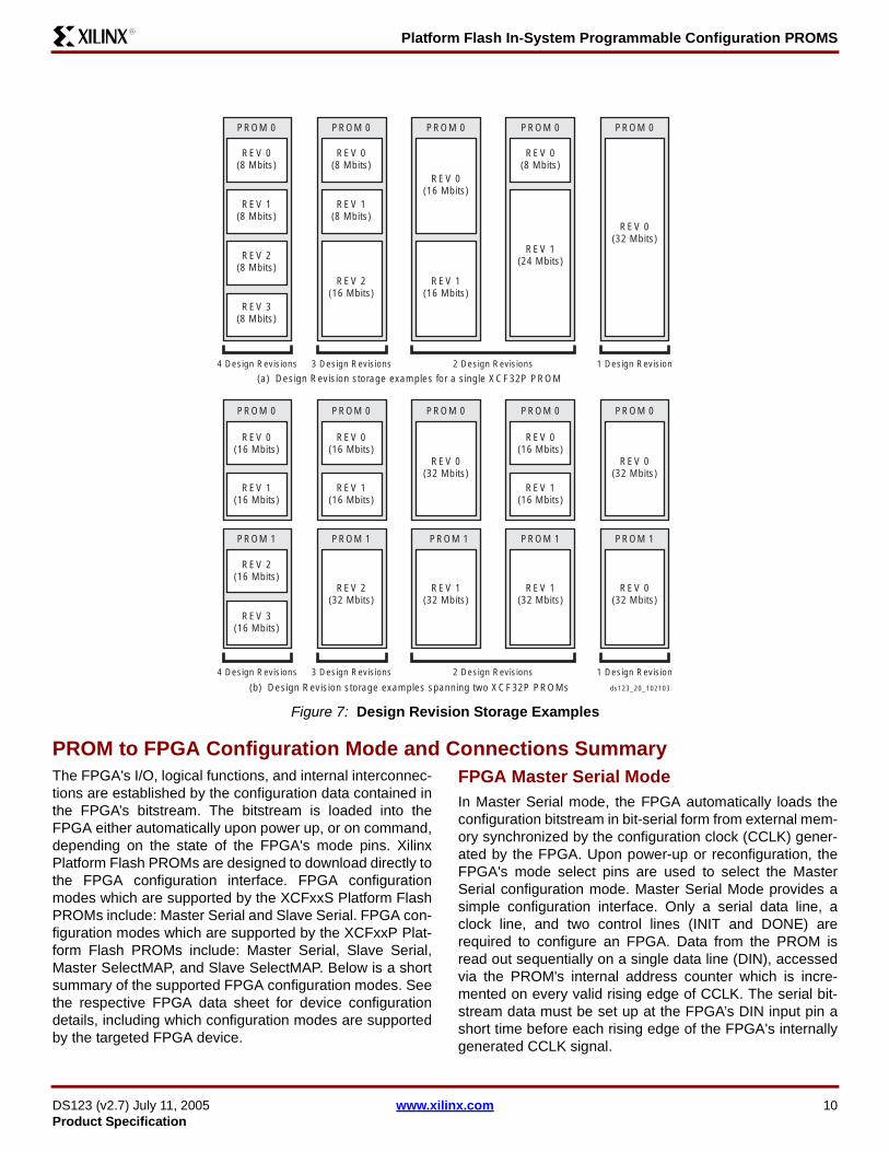
Platform Flash In-System Programmable Configuration PROMS
DS123 (v27) July 11 2005 wwwxilinxcom 11Product Specification
R
Typically a wide range of frequencies can be selected forthe FPGArsquos internally generated CCLK which always startsat a slow default frequency The FPGArsquos bitstream containsconfiguration bits which can switch CCLK to a higher fre-quency for the remainder of the Master Serial configurationsequence The desired CCLK frequency is selected duringbitstream generationConnecting the FPGA device to the configuration PROM forMaster Serial Configuration Mode (Figure 8)bull The DATA output of the PROM(s) drive the DIN input of
the lead FPGA devicebull The Master FPGA CCLK output drives the CLK input(s)
of the PROM(s) bull The CEO output of a PROM drives the CE input of the
next PROM in a daisy chain (if any)bull The OERESET pins of all PROMs are connected to
the INIT_B pins of all FPGA devices This connection assures that the PROM address counter is reset before the start of any (re)configuration
bull The PROM CE input can be driven from the DONE pin The CE input of the first (or only) PROM can be driven by the DONE output of all target FPGA devices provided that DONE is not permanently grounded CE can also be permanently tied Low but this keeps the DATA output active and causes an unnecessary ICC active supply current (DC Characteristics Over Operating Conditions)
bull The PROM CF pin is typically connected to the FPGAs PROG_B (or PROGRAM) input For the XCFxxP only the CF pin is a bidirectional pin If the XCFxxP CF pin is not connected to the FPGAs PROG_B (or PROGRAM) input then the pin should be tied High
FPGA Slave Serial ModeIn Slave Serial mode the FPGA loads the configuration bit-stream in bit-serial form from external memory synchro-nized by an externally supplied clock Upon power-up orreconfiguration the FPGAs mode select pins are used toselect the Slave Serial configuration mode Slave SerialMode provides a simple configuration interface Only aserial data line a clock line and two control lines (INIT andDONE) are required to configure an FPGA Data from thePROM is read out sequentially on a single data line (DIN)accessed via the PROMs internal address counter which isincremented on every valid rising edge of CCLK The serialbitstream data must be set up at the FPGArsquos DIN input pin ashort time before each rising edge of the externally providedCCLKConnecting the FPGA device to the configuration PROM forSlave Serial Configuration Mode (Figure 9)bull The DATA output of the PROM(s) drive the DIN input of
the lead FPGA devicebull The PROM CLKOUT (for XCFxxP only) or an external
clock source drives the FPGAs CCLK input
bull The CEO output of a PROM drives the CE input of the next PROM in a daisy chain (if any)
bull The OERESET pins of all PROMs are connected to the INIT_B (or INIT) pins of all FPGA devices This connection assures that the PROM address counter is reset before the start of any (re)configuration
bull The PROM CE input can be driven from the DONE pin The CE input of the first (or only) PROM can be driven by the DONE output of all target FPGA devices provided that DONE is not permanently grounded CE can also be permanently tied Low but this keeps the DATA output active and causes an unnecessary ICC active supply current (DC Characteristics Over Operating Conditions)
bull The PROM CF pin is typically connected to the FPGAs PROG_B (or PROGRAM) input For the XCFxxP only the CF pin is a bidirectional pin If the XCFxxP CF pin is not connected to the FPGAs PROG_B (or PROGRAM) input then the pin should be tied High
Serial Daisy ChainMultiple FPGAs can be daisy-chained for serial configura-tion from a single source After a particular FPGA has beenconfigured the data for the next device is routed internallyto the FPGArsquos DOUT pin Typically the data on the DOUTpin changes on the falling edge of CCLK although for somedevices the DOUT pin changes on the rising edge of CCLKConsult the respective device data sheets for detailed infor-mation on a particular FPGA device For clocking thedaisy-chained configuration either the first FPGA in thechain can be set to Master Serial generating the CCLKwith the remaining devices set to Slave Serial (Figure 10)or all the FPGA devices can be set to Slave Serial and anexternally generated clock can be used to drive the FPGAsconfiguration interface
FPGA Master SelectMAP (Parallel) Mode(1)
In Master SelectMAP mode byte-wide data is written intothe FPGA typically with a BUSY flag controlling the flow ofdata synchronized by the configuration clock (CCLK) gen-erated by the FPGA Upon power-up or reconfiguration theFPGAs mode select pins are used to select the MasterSelectMAP configuration mode The configuration interfacetypically requires a parallel data bus a clock line and twocontrol lines (INIT and DONE) In addition the FPGArsquos ChipSelect Write and BUSY pins must be correctly controlled toenable SelectMAP configuration The configuration data isread from the PROM byte by byte on pins [D0D7]accessed via the PROMs internal address counter which isincremented on every valid rising edge of CCLK The bit-stream data must be set up at the FPGArsquos [D0D7] input
1 The Master SelectMAP (Parallel) FPGA configuration mode is sup-ported only by the XCFxxP Platform Flash PROM This mode is not supported by the XCFxxS Platform Flash PROM
Platform Flash In-System Programmable Configuration PROMS
DS123 (v27) July 11 2005 wwwxilinxcom 12Product Specification
R
pins a short time before each rising edge of the FPGAsinternally generated CCLK signal If BUSY is asserted(High) by the FPGA the configuration data must be helduntil BUSY goes Low An external data source or externalpull-down resistors must be used to enable the FPGAsactive Low Chip Select (CS or CS_B) and Write (WRITE orRDWR_B) signals to enable the FPGAs SelectMAP config-uration process The Master SelectMAP configuration interface is clocked bythe FPGArsquos internal oscillator Typically a wide range of fre-quencies can be selected for the internally generated CCLKwhich always starts at a slow default frequency The FPGArsquosbitstream contains configuration bits which can switchCCLK to a higher frequency for the remainder of the MasterSelectMAP configuration sequence The desired CCLK fre-quency is selected during bitstream generationAfter configuration the pins of the SelectMAP port can beused as additional user IO Alternatively the port can beretained using the persist optionConnecting the FPGA device to the configuration PROM forMaster SelectMAP (Parallel) Configuration Mode(Figure 11)bull The DATA outputs of the PROM(s) drive the [D0D7]
input of the lead FPGA devicebull The Master FPGA CCLK output drives the CLK input(s)
of the PROM(s) bull The CEO output of a PROM drives the CE input of the
next PROM in a daisy chain (if any)bull The OERESET pins of all PROMs are connected to
the INIT_B pins of all FPGA devices This connection assures that the PROM address counter is reset before the start of any (re)configuration
bull The PROM CE input can be driven from the DONE pin The CE input of the first (or only) PROM can be driven by the DONE output of all target FPGA devices provided that DONE is not permanently grounded CE can also be permanently tied Low but this keeps the DATA output active and causes an unnecessary ICC active supply current (DC Characteristics Over Operating Conditions)
bull For high-frequency parallel configuration the BUSY pins of all PROMs are connected to the FPGAs BUSY output This connection assures that the next data transition for the PROM is delayed until the FPGA is ready for the next configuration data byte
bull The PROM CF pin is typically connected to the FPGAs PROG_B (or PROGRAM) input For the XCFxxP only the CF pin is a bidirectional pin If the XCFxxP CF pin is not connected to the FPGAs PROG_B (or PROGRAM) input then the pin should be tied High
FPGA Slave SelectMAP (Parallel) Mode(1)
In Slave SelectMAP mode byte-wide data is written into theFPGA typically with a BUSY flag controlling the flow of
data synchronized by an externally supplied configurationclock (CCLK) Upon power-up or reconfiguration theFPGAs mode select pins are used to select the SlaveSelectMAP configuration mode The configuration interfacetypically requires a parallel data bus a clock line and twocontrol lines (INIT and DONE) In addition the FPGArsquos ChipSelect Write and BUSY pins must be correctly controlled toenable SelectMAP configuration The configuration data isread from the PROM byte by byte on pins [D0D7]accessed via the PROMs internal address counter which isincremented on every valid rising edge of CCLK The bit-stream data must be set up at the FPGArsquos [D0D7] inputpins a short time before each rising edge of the providedCCLK If BUSY is asserted (High) by the FPGA the config-uration data must be held until BUSY goes Low An externaldata source or external pull-down resistors must be used toenable the FPGAs active Low Chip Select (CS or CS_B)and Write (WRITE or RDWR_B) signals to enable theFPGAs SelectMAP configuration process After configuration the pins of the SelectMAP port can beused as additional user IO Alternatively the port can beretained using the persist optionConnecting the FPGA device to the configuration PROM forSlave SelectMAP (Parallel) Configuration Mode(Figure 12)bull The DATA outputs of the PROM(s) drives the [D0D7]
inputs of the lead FPGA devicebull The PROM CLKOUT (for XCFxxP only) or an external
clock source drives the FPGAs CCLK inputbull The CEO output of a PROM drives the CE input of the
next PROM in a daisy chain (if any)bull The OERESET pins of all PROMs are connected to
the INIT_B pins of all FPGA devices This connection assures that the PROM address counter is reset before the start of any (re)configuration
bull The PROM CE input can be driven from the DONE pin The CE input of the first (or only) PROM can be driven by the DONE output of all target FPGA devices provided that DONE is not permanently grounded CE can also be permanently tied Low but this keeps the DATA output active and causes an unnecessary ICC active supply current (DC Characteristics Over Operating Conditions)
bull For high-frequency parallel configuration the BUSY pins of all PROMs are connected to the FPGAs BUSY output This connection assures that the next data transition for the PROM is delayed until the FPGA is ready for the next configuration data byte
bull The PROM CF pin is typically connected to the FPGAs
1 The Slave SelectMAP (Parallel) FPGA configuration mode is sup-ported only by the XCFxxP Platform Flash PROMsThis mode is not supported by the XCFxxS Platform Flash PROM
Platform Flash In-System Programmable Configuration PROMS
DS123 (v27) July 11 2005 wwwxilinxcom 13Product Specification
R
PROG_B (or PROGRAM) input For the XCFxxP only the CF pin is a bidirectional pin If the XCFxxP CF pin is not connected to the FPGAs PROG_B (or PROGRAM) input then the pin should be tied High
FPGA SelectMAP (Parallel) Device Chaining(1)
Multiple Virtex-II FPGAs can be configured using theSelectMAP mode and be made to start up simultaneouslyTo configure multiple devices in this way wire the individualCCLK DONE INIT Data ([D0D7]) Write (WRITE orRDWR_B) and BUSY pins of all the devices in parallel If alldevices are to be configured with the same bitstream read-back is not being used and the CCLK frequency selecteddoes not require the use of the BUSY signal the CS_B pinscan be connected to a common line so all of the devices areconfigured simultaneously (Figure 13)With additional control logic the individual devices can beloaded separately by asserting the CS_B pin of each devicein turn and then enabling the appropriate configuration dataThe PROM can also store the individual bitstreams for eachFPGA for SelectMAP configuration in separate design revi-sions When design revisioning is utilized additional controllogic can be used to select the appropriate bitstream byasserting the EN_EXT_SEL pin and using theREV_SEL[10] pins to select the required bitstream whileasserting the CS_B pin for the FPGA the bitstream is target-ing (Figure 14) For clocking the parallel configuration chain either the firstFPGA in the chain can be set to Master SelectMAP gener-ating the CCLK with the remaining devices set to SlaveSelectMAP or all the FPGA devices can be set to SlaveSelectMAP and an externally generated clock can be usedto drive the configuration interface Again the respectivedevice data sheets should be consulted for detailed infor-mation on a particular FPGA device including which config-uration modes are supported by the targeted FPGA device
Cascading Configuration PROMsWhen configuring multiple FPGAs in a serial daisy chainconfiguring multiple FPGAs in a SelectMAP parallel chainor configuring a single FPGA requiring a larger configura-tion bitstream cascaded PROMs provide additional mem-ory (Figure 10 Figure 13 Figure 14 and Figure 15)Multiple Platform Flash PROMs can be concatenated byusing the CEO output to drive the CE input of the down-stream device The clock signal and the data outputs of allPlatform Flash PROMs in the chain are interconnectedAfter the last data from the first PROM is read the firstPROM asserts its CEO output Low and drives its outputs to
a high-impedance state The second PROM recognizes theLow level on its CE input and immediately enables its out-putsAfter configuration is complete address counters of all cas-caded PROMs are reset if the PROM OERESET pin goesLow or CE goes HighWhen utilizing the advanced features for the XCFxxP Plat-form Flash PROM including the clock output (CLKOUT)option decompression option or design revisioning pro-gramming files which span cascaded PROM devices canonly be created for cascaded chains containing onlyXCFxxP PROMs If the advanced features are not usedthen cascaded PROM chains can contain both XCFxxP andXCFxxS PROMs
Initiating FPGA ConfigurationThe options for initiating FPGA configuration via the Plat-form Flash PROM include1 Automatic configuration on power up2 Applying an external PROG_B (or PROGRAM) pulse3 Applying the JTAG CONFIG instructionFollowing the FPGArsquos power-on sequence or the assertionof the PROG_B (or PROGRAM) pin the FPGArsquos configura-tion memory is cleared the configuration mode is selectedand the FPGA is ready to accept a new configuration bit-stream The FPGArsquos PROG_B pin can be controlled by anexternal source or alternatively the Platform Flash PROMsincorporate a CF pin that can be tied to the FPGArsquosPROG_B pin Executing the CONFIG instruction throughJTAG pulses the CF output Low once for 300-500 ns reset-ting the FPGA and initiating configuration The iMPACTsoftware can issue the JTAG CONFIG command to initiateFPGA configuration by setting the Load FPGA option When using the XCFxxP Platform Flash PROM with designrevisioning enabled the CF pin should always be con-nected to the PROG_B (or PROGRAM) pin on the FPGA toensure that the current design revision selection is sampledwhen the FPGA is reset The XCFxxP PROM samples thecurrent design revision selection from the externalREV_SEL pins or the internal programmable RevisionSelect bits on the rising edge of CF When the JTAG CON-FIG command is executed the XCFxxP will sample the newdesign revision before initiating the FPGA configurationsequence When using the XCFxxP Platform Flash PROMwithout design revisioning if the CF pin is not connected tothe FPGA PROG_B (or PROGRAM) pin then the XCFxxPCF pin should be tied High
1 The SelectMAP (Parallel) FPGA configuration modes are supported only by the XCFxxP Platform Flash PROMThese modes are not sup-ported by the XCFxxS Platform Flash PROM
Platform Flash In-System Programmable Configuration PROMS
DS123 (v27) July 11 2005 wwwxilinxcom 14Product Specification
R
Configuration PROM to FPGA Device Interface Connection Diagrams
Figure 8 Configuring in Master Serial Mode
Xilinx FPGAMaster Serial
DIN
CCLK
DONE
INIT_B
PROG_B
TDI
TMS
TCK
GND
MODE PINS(1)
DOUT
TDO
VCCJ VCCO VCCINT
DIN
CCLK
DONE
INIT_B
PROG_B
DIN
CCLK
DONE
INIT_B
PROG_B
47
kΩ
47
kΩ (1)
VCCO(2)
OPTIONALDaisy-chainedSlave FPGAs with differentconfigurations
OPTIONALSlave FPGAs with identicalconfigurations
TDI
TMS
TCK
TDO
Notes1 For Mode pin connections and DONE pin pullup value refer to the appropriate FPGA data sheet2 For compatible voltages refer to the appropriate data sheet3 For the XCFxxS the CF pin is an output pin For the XCFxxP the CF pin is a bidirectional pin
Platform Flash PROM
VCCINT
VCCO(2)
VCCJ(2)
TDI
TMS
TCK
GND
D0
CLK
CE
CEO
OERESET
CF(3)
TDO
ds123_11_100804
Platform Flash In-System Programmable Configuration PROMS
DS123 (v27) July 11 2005 wwwxilinxcom 15Product Specification
R
Figure 9 Configuring in Slave Serial Mode
Xilinx FPGASlave Serial
DIN
CCLK
DONE
INIT_B
PROG_B
TDI
TMS
TCK
GND
MODE PINS(1)
DOUT
TDO
VCCJ VCCO VCCINT
DIN
CCLK
DONE
INIT_B
PROG_B
DIN
CCLK
DONE
INIT_B
PROG_B
47
kΩ
47
kΩ (1)
VCCO(2)
OPTIONALDaisy-chainedSlave FPGAs with differentconfigurations
OPTIONALSlave FPGAs with identicalconfigurations
TDI
TMS
TCK
TDO
Notes1 For Mode pin connections and DONE pin pullup value refer to the appropriate FPGA data sheet2 For compatible voltages refer to the appropriate data sheet3 In Slave Serial mode the configuration interface can be clocked by an external oscillator or optionallymdashfor the XCFxxP Platform Flash PROM onlymdashthe CLKOUT signal can be used to drive the FPGAs configuration clock (CCLK) If the XCFxxP PROMs CLKOUT signal is used then it must be tied to a 47KΩ resistor pulled up to VCCO4 For the XCFxxS the CF pin is an output pin For the XCFxxP the CF pin is a bidirectional pin
Platform Flash PROM
VCCINT
VCCO(2)
VCCJ(2)
TDI
TMS
TCK
GND
D0
CLK(3)
CE
CEO
OERESET
CF(4)
TDO
ds123_12_070505
External (3)
Oscillator
Platform Flash In-System Programmable Configuration PROMS
DS123 (v27) July 11 2005 wwwxilinxcom 16Product Specification
R
Figure 10 Configuring Multiple Devices MasterSlave Serial Mode
Platform Flash PROM
First PROM(PROM 0)
VCCINT
VCCO(2)
VCCJ(2)
TDI
TMS
TCK
D0
CLK
CE
CEO
OERESET
CF(3)
TDO
Xilinx FPGAMaster Serial
DIN
CCLK
DONE
INIT_B
PROG_B
TDI
TMS
TCK
MODE PINS(1)
DOUT
TDO
VCCJ VCCO VCCINT
47
kΩ
47
kΩ (1)
VCCO(2)
TDI
TMS
TCK
TDO
Notes1 For Mode pin connections and DONE pin pullup value refer to the appropriate FPGA data sheet2 For compatible voltages refer to the appropriate data sheet3 For the XCFxxS the CF pin is an output pin For the XCFxxP the CF pin is a bidirectional pin
Xilinx FPGASlave Serial
DIN
CCLK
DONE
INIT_B
PROG_B
TDI
TMS
TCK
Platform Flash PROM
Cascaded PROM(PROM 1)
VCCINT
VCCO(2)
VCCJ(2)
TDI
TMS
TCK
D0
CLK
CE
CEO
OERESET
CF(3)
TDO
VCCJ VCCO VCCINT
MODE PINS(1)
TDO
ds123_13_100804
GND
GNDGND
GND
Platform Flash In-System Programmable Configuration PROMS
DS123 (v27) July 11 2005 wwwxilinxcom 17Product Specification
R
Figure 11 Configuring in Master SelectMAP Mode
XCFxxPPlatform Flash PROM
VCCINT
VCCO(2)
VCCJ(2)
TDI
TMS
TCK
GND
D[07]
CLK
CE
CEO
OERESET
CF(5)
BUSY(4)
TDO
Xilinx FPGAMaster SelectMAP
D[07]
CCLK
DONE
INIT_B
PROG_B
BUSY(4)
TDI
TMS
TCK
GND
MODE PINS(1)
RDWR_B
CS_B
TDO
VCCJ VCCO VCCINT
D[07]
CCLK
DONE
INIT_B
PROG_B
BUSY(4)
47
kΩ
47
kΩ (1)
VCCO(2)
OPTIONALSlave FPGAs with identicalconfigurations
TDI
TMS
TCK
TDO
Notes1 For Mode pin connections and DONE pin pullup value refer to the appropriate FPGA data sheet2 For compatible voltages refer to the appropriate data sheet3 CS_B (or CS) and RDWR_B (or WRITE) must be either driven Low or pulled down exernally One option is shown4 The BUSY pin is only available with the XCFxxP Platform Flash PROM and the connection is only required for high-frequency SelectMAP mode configuration For BUSY pin requirements refer to the appropriate FPGA data sheet5 For the XCFxxP the CF pin is a bidirectional pin
1KΩ
1KΩ
IO(3)
IO(3)
ds123_14_100804
Platform Flash In-System Programmable Configuration PROMS
DS123 (v27) July 11 2005 wwwxilinxcom 18Product Specification
R
Figure 12 Configuring in Slave SelectMAP Mode
XCFxxPPlatform Flash PROM
VCCINT
VCCO(2)
VCCJ(2)
TDI
TMS
TCK
GND
D[07]
CLK(5)
CE
CEO
OERESET
CF(6)
BUSY(4)
TDO
Xilinx FPGASlave SelectMAP
D[07]
CCLK
DONE
INIT_B
PROG_B
BUSY(4)
TDI
TMS
TCK
GND
MODE PINS(1)
RDWR_B
CS_B
TDO
VCCJ VCCO VCCINT
D[07]
CCLK
DONE
INIT_B
PROG_B
BUSY(4)
47
kΩ
47
kΩ (1)
VCCO(2)
OPTIONALSlave FPGAs with identicalconfigurations
TDI
TMS
TCK
TDO
Notes1 For Mode pin connections and DONE pin pullup value refer to the appropriate FPGA data sheet2 For compatible voltages refer to the appropriate data sheet3 CS_B (or CS) and RDWR_B (or WRITE) must be either driven Low or pulled down exernally One option is shown4 The BUSY pin is only available with the XCFxxP Platform Flash PROM and the connection is only required for high-frequency SelectMAP mode configuration For BUSY pin requirements refer to the appropriate FPGA data sheet5 In Slave SelectMAP mode the configuration interface can be clocked by an external oscillator or optionally the CLKOUT signal can be used to drive the FPGAs configuration clock (CCLK) If the XCFxxP PROMs CLKOUT signal is used then it must be tied to a 47KΩ resistor pulled up to VCCO6 For the XCFxxP the CF pin is a bidirectional pin
1KΩ
1KΩ
IO(3)
IO(3)
ds123_15_070505
External (5)
Oscillator
Platform Flash In-System Programmable Configuration PROMS
DS123 (v27) July 11 2005 wwwxilinxcom 19Product Specification
R
Figure 13 Configuring Multiple Devices with Identical Patterns in MasterSlave SelectMAP Mode
XCFxxPPlatform Flash PROM
First PROM(PROM 0)
VCCINT
VCCO(2)
VCCJ(2)
TDI
TMS
TCK
GND
D[07]
CLK
CE
CEO
OERESET
CF(5)
BUSY(4)
TDO
Xilinx FPGAMaster SelectMAP
D[07]
CCLK
DONE
INIT_B
PROG_B
BUSY(4)
TDI
TMS
TCK
GND
MODE PINS(1)
TDO
VCCJ VCCO VCCINT
47
kΩ
47
kΩ (1)
VCCO(2)
TDI
TMS
TCK
TDO
Notes1 For Mode pin connections and DONE pin pullup value refer to the appropriate FPGA data sheet2 For compatible voltages refer to the appropriate data sheet3 CS_B (or CS) and RDWR_B (or WRITE) must be either driven Low or pulled down exernally One option is shown4 The BUSY pin is only available with the XCFxxP Platform Flash PROM and the connection is only required for high-frequency SelectMAP mode configuration For BUSY pin requirements refer to the appropriate FPGA data sheet5 For the XCFxxP the CF pin is a bidirectional pin
Xilinx FPGASlave SelectMAP
D[07]
CCLK
DONE
INIT_B
PROG_B
BUSY(4)
TDI
TMS
TCK
GND
XCFxxPPlatform Flash PROM
Cascaded PROM(PROM 1)
VCCINT
VCCO(2)
VCCJ(2)
TDI
TMS
TCK
GND
D[07]
CLK
CE
CEO
OERESET
CF(5)
BUSY(4)
TDO
VCCJ VCCO VCCINT
MODE PINS(1)
TDO
ds123_16_100804
1KΩ1K
Ω
IO(3)
IO(3)
1KΩ1K
Ω
IO(3)
IO(3)RDWR_B
CS_B
RDWR_B
CS_B
Platform Flash In-System Programmable Configuration PROMS
DS123 (v27) July 11 2005 wwwxilinxcom 20Product Specification
R
Figure 14 Configuring Multiple Devices with Design Revisioning in Slave Serial Mode
XCFxxPPlatform Flash PROM
First PROM(PROM 0)
VCCINT
VCCO(2)
VCCJ(2)
TDI
TMS
TCK
EN_EXT_SEL
REV_SEL[10]
D0
CLK(3)
CE
CEO
OERESET
CF(4)
TDO
Xilinx FPGASlave Serial
DIN
CCLK
DONE
INIT_B
PROG_B
TDI
TMS
TCK
VCCJ VCCO VCCINT
47
kΩ
47
kΩ
(1)
VCCO(2)
TDI
TMS
TCK
TDO
1 For Mode pin connections and DONE pin pullup value refer to the appropriate FPGA data sheet
2 For compatible voltages refer to the appropriate data sheet3 In Slave Serial mode the configuration interface can be clocked by an external oscillator or optionally the CLKOUT signal can be used to drive the FPGAs configuration clock (CCLK) If the XCFxxP PROMs CLKOUT signal is used then it must be tied to a 47KΩ resistor pulled up to VCCO4 For the XCFxxP the CF pin is a bidirectional pin
XCFxxPPlatform Flash PROM
Cascaded PROM(PROM 1)
VCCINT
VCCO(2)
VCCJ(2)
TDI
TMS
TCK
EN_EXT_SEL
REV_SEL[10]
D0
CLK(3)
CE
CEO
OERESET
CF(4)
TDO
VCCJ VCCO VCCINT
ds123_17_070505
Design RevisionControl Logic
EN_EXT_SEL
REV_SEL[10]
DONE
CF PROG_B
Xilinx FPGASlave Serial
DIN
CCLK
DONE
INIT_B
PROG_B
TDI
TMS
TCK
MODE PINS(1)
TDO
GNDGND
GND
DOUT
MODE PINS(1)
GND
External (3)
Oscillator
Platform Flash In-System Programmable Configuration PROMS
DS123 (v27) July 11 2005 wwwxilinxcom 21Product Specification
R
Figure 15 Configuring Multiple Devices with Design Revisioning in Slave SelectMAP Mode
XCFxxPPlatform Flash PROM
First PROM(PROM 0)
VCCINT
VCCO(2)
VCCJ(2)
TDI
TMS
TCK
EN_EXT_SEL
REV_SEL[10]
GND
D[07]
CLK(5)
CE
CEO
OERESET
CF(6)
BUSY(4)
TDO
Xilinx FPGASlave SelectMAP
D[07]
CCLK
DONE
INIT_B
PROG_B
BUSY(4)
TDI
TMS
TCK
MODE PINS(1)
RDWR_B
CS_B
TDO
VCCJ VCCO VCCINT
47
kΩ
47
kΩ
(1)
VCCO(2)
TDI
TMS
TCK
TDO
Notes
1 For Mode pin connections and DONE pin pullup value refer to the appropriate FPGA data sheet
2 For compatible voltages refer to the appropriate data sheet
3 RDWR_B (or WRITE) must be either driven Low or pulled down exernally One option is shown
4 The BUSY pin is only available with the XCFxxP Platform Flash PROM and the connection is only required for high frequency SelectMAP mode configuration For BUSY pin requirements refer to the appropriate FPGA data sheet
5 In Slave SelectMAP mode the configuration interface can be clocked by an external oscillator or optionally the CLKOUT signal can be used to drive the FPGAs configuration clock (CCLK) If the XCFxxP PROMs CLKOUT signal is used then it must be tied to a 47KΩ resistor pulled up to VCCO6 For the XCFxxP the CF pin is a bidirectional pin
Xilinx FPGASlave SelectMAP
D[07]
CCLK
DONE
INIT_B
PROG_B
BUSY(4)
TDI
TMS
TCK
MODE PINS(1)
RDWR_B
CS_B
TDO
XCFxxPPlatform Flash PROM
Cascaded PROM(PROM 1)
VCCINT
VCCO(2)
VCCJ(2)
TDI
TMS
TCK
EN_EXT_SEL
REV_SEL[10]
GND
D[07]
CLK(5)
CE
CEO
OERESET
CF(6)
BUSY(4)
TDO
VCCJ VCCO VCCINT
1KΩ
IO(3)
1KΩ
IO(3)
EN_EXT_SEL
REV_SEL[10]
CF
DONE
PROG_B
CS_B[10]
Design
Revision
Control
Logic
GND GND
ds123_18_070505
External (5)
Oscillator
Platform Flash In-System Programmable Configuration PROMS
DS123 (v27) July 11 2005 wwwxilinxcom 22Product Specification
R
Reset and Power-On Reset ActivationAt power up the device requires the VCCINT power supplyto monotonically rise to the nominal operating voltage withinthe specified VCCINT rise time If the power supply cannotmeet this requirement then the device might not performpower-on reset properly During the power-up sequenceOERESET is held Low by the PROM Once the requiredsupplies have reached their respective POR (Power OnReset) thresholds the OERESET release is delayed (TOERminimum) to allow more margin for the power supplies tostabilize before initiating configuration The OERESET pinis connected to an external 47kΩ pull-up resistor and alsoto the target FPGAs INIT pin For systems utilizing slow-ris-ing power supplies an additional power monitoring circuitcan be used to delay the target configuration until the sys-tem power reaches minimum operating voltages by holdingthe OERESET pin Low When OERESET is released theFPGArsquos INIT pin is pulled High allowing the FPGAs config-uration sequence to begin If the power drops below the
power-down threshold (VCCPD) the PROM resets andOERESET is again held Low until the after the POR thresh-old is reached OERESET polarity is not programmableThese power-up requirements are shown graphically inFigure 16For a fully powered Platform Flash PROM a reset occurswhenever OERESET is asserted (Low) or CE is deas-serted (High) The address counter is reset CEO is drivenHigh and the remaining outputs are placed in a high-imped-ance stateNotes1 The XCFxxS PROM only requires VCCINT to rise above
its POR threshold before releasing OERESET 2 The XCFxxP PROM requires both VCCINT to rise above
its POR threshold and for VCCO to reach the recommended operating voltage level before releasing OERESET
IO Input Voltage Tolerance and Power Sequencing The IOs on each re-programmable Platform Flash PROMare fully 33V-tolerant This allows 3V CMOS signals to con-nect directly to the inputs without damage The core powersupply (VCCINT) JTAG pin power supply (VCCJ) outputpower supply (VCCO) and external 3V CMOS IO signalscan be applied in any order Additionally for the XCFxxS PROM only when VCCO is sup-plied at 25V or 33V and VCCINT is supplied at 33V theIOs are 5V-tolerant This allows 5V CMOS signals to con-nect directly to the inputs on a powered XCFxxS PROMwithout damage Failure to power the PROM correctly whilesupplying a 5V input signal may result in damage to theXCFxxS device
Standby ModeThe PROM enters a low-power standby mode whenever CEis deasserted (High) In standby mode the address counteris reset CEO is driven High and the remaining outputs areplaced in a high-impedance state regardless of the state ofthe OERESET input For the device to remain in thelow-power standby mode the JTAG pins TMS TDI andTDO must not be pulled Low and TCK must be stopped(High or Low)When using the FPGA DONE signal to drive the PROM CEpin High to reduce standby power after configuration anexternal pull-up resistor should be used Typically a 330Ωpull-up resistor is used but refer to the appropriate FPGAdata sheet for the recommended DONE pin pull-up value Ifthe DONE circuit is connected to an LED to indicate FPGA
Figure 16 Platform Flash PROM Power-Up Requirements
TOER
VCCINT
VCCPOR
VCCPD
200 micros ramp50 ms ramp
TOER TRST
TIME (ms)
A slow-ramping VCCINT supply may still be below the minimum operating voltage when OERESET is released In this case the configuration sequence must be delayed until both VCCINT and VCCO have reached their recommended operating conditions
Recommended Operating Range
Delay or RestartConfiguration
ds123_21_103103
Platform Flash In-System Programmable Configuration PROMS
DS123 (v27) July 11 2005 wwwxilinxcom 23Product Specification
R
configuration is complete and is also connected to thePROM CE pin to enable low-power standby mode then anexternal buffer should be used to drive the LED circuit to
ensure valid transitions on the PROMrsquos CE pin If low-powerstandby mode is not required for the PROM then the CE pinshould be connected to ground
DC Electrical CharacteristicsThis data sheet is a Preliminary data sheet The DC characteristics are based on characterization rather than simulationFurther characteristic changes are not expected
bullAbsolute Maximum Ratings page 24bullSupply Voltage Requirements for Power-On Reset and Power-Down page 24bullRecommended Operating Conditions page 25bullQuality and Reliability Characteristics page 25bullDC Characteristics Over Operating Conditions page 26
Table 9 Truth Table for XCFxxS PROM Control InputsControl Inputs
Internal Address
Outputs
OERESET CE DATA CEO ICC
High LowIf address lt TC(2) increment Active High Active
If address = TC(2) dont change High-Z Low Reduced
Low Low Held reset High-Z High Active
X(1) High Held reset High-Z High Standby
Notes 1 X = donrsquot care2 TC = Terminal Count = highest address value TC + 1 = address 0
Table 10 Truth Table for XCFxxP PROM Control InputsControl Inputs
Internal Address
Outputs
OERESET CE CF BUSY(5) DATA CEO CLKOUT ICC
High Low High Low
If address lt TC(2) and address lt EA(3) increment Active High Active Active
If address lt TC(2) and address = EA(3) dont change High-Z High High-Z Reduced
Else If address = TC(2) dont change High-Z Low High-Z Reduced
High Low High High Unchanged Active and Unchanged High Active Active
High Low uarr X(1) Reset(4) Active High Active Active
Low Low X X Held reset(4) High-Z High High-Z Active
X High X X Held reset(4) High-Z High High-Z Standby
Notes 1 X = donrsquot care2 TC = Terminal Count = highest address value TC + 1 = address 03 For the XCFxxP with Design Revisioning enabled EA = end address (last address in the selected design revision) 4 For the XCFxxP with Design Revisioning enabled Reset = address reset to the beginning address of the selected bank If Design Revisioning is not
enabled then Reset = address reset to address 05 The BUSY input is only enabled when the XCFxxP is programmed for parallel data output and decompression is not enabled
Platform Flash In-System Programmable Configuration PROMS
DS123 (v27) July 11 2005 wwwxilinxcom 24Product Specification
R
AC Electrical CharacteristicsThis data sheet is a Preliminary data sheet The AC characteristics are based on characterization rather than simulationFurther characteristic changes are not expected
bullAC Characteristics Over Operating Conditions page 28bullAC Characteristics Over Operating Conditions When Cascading page 32
Absolute Maximum Ratings
Supply Voltage Requirements for Power-On Reset and Power-Down
Symbol DescriptionXCF01S XCF02S
XCF04SXCF08P XCF16P
XCF32P Units
VCCINT Internal supply voltage relative to GND ndash05 to +40 ndash05 to +27 V
VCCO IO supply voltage relative to GND ndash05 to +40 ndash05 to +40 V
VCCJ JTAG IO supply voltage relative to GND ndash05 to +40 ndash05 to +40 V
VIN Input voltage with respect to GNDVCCO lt 25V ndash05 to +36 ndash05 to +36 V
VCCO ge 25V ndash05 to +55 ndash05 to +36 V
VTS Voltage applied to High-Z outputVCCO lt 25V ndash05 to +36 ndash05 to +36 V
VCCO ge 25V ndash05 to +55 ndash05 to +36 V
TSTG Storage temperature (ambient) ndash65 to +150 ndash65 to +150 degC
TJ Junction temperature +125 +125 degC
Notes 1 Maximum DC undershoot below GND must be limited to either 05V or 10 mA whichever is easier to achieve During transitions the device pins can
undershoot to ndash20V or overshoot to +70V provided this over- or undershoot lasts less then 10 ns and with the forcing current being limited to 200 mA
2 Stresses beyond those listed under Absolute Maximum Ratings might cause permanent damage to the device These are stress ratings only and functional operation of the device at these or any other conditions beyond those listed under Operating Conditions is not implied Exposure to Absolute Maximum Ratings conditions for extended periods of time adversely affects device reliability
3 For soldering guidelines see the information on Packaging and Thermal Characteristics at wwwxilinxcom
Symbol Description
XCF01S XCF02S XCF04S
XCF08P XCF16P XCF32P
UnitsMin Max Min Max
TVCC VCCINT rise time from 0V to nominal voltage(2) 02 50 02 50 ms
VCCPOR POR threshold for the VCCINT supply 1 - 05 - V
TOER OERESET release delay following POR(3) 05 3 05 30 ms
VCCPD Power-down threshold for VCCINT supply - 1 - 05 V
TRSTTime required to trigger a device reset when the VCCINT supply drops below the maximum VCCPD threshold 10 - 10 - ms
Notes 1 VCCINT VCCO and VCCJ supplies may be applied in any order2 At power up the device requires the VCCINT power supply to monotonically rise to the nominal operating voltage within the specified TVCC rise time
If the power supply cannot meet this requirement then the device might not perform power-on-reset properly See Figure 16 page 223 If the VCCINT and VCCO supplies do not reach their respective recommended operating conditions before the OERESET pin is released then the
configuration data from the PROM will not be available at the recommended threshold levels The configuration sequence must be delayed until both VCCINT and VCCO have reached their recommended operating conditions
huffman
XCF08P
huffman
XCF08P
Platform Flash In-System Programmable Configuration PROMS
DS123 (v27) July 11 2005 wwwxilinxcom 25Product Specification
R
Recommended Operating Conditions
Quality and Reliability Characteristics
Symbol Description
XCF01S XCF02S XCF04S XCF08P XCF16P XCF32P
UnitsMin Typ Max Min Typ MaxVCCINT Internal voltage supply 30 33 36 165 18 20 V
VCCOSupply voltage for output drivers
33V Operation 30 33 36 30 33 36 V
25V Operation 23 25 27 23 25 27 V
18V Operation 17 18 19 17 18 19 V
15V Operation - - - TBD 15 TBD V
VCCJSupply voltage for JTAG output drivers
33V Operation 30 33 36 30 33 36 V
25V Operation 23 25 27 23 25 27 V
VILLow-level input voltage
33V Operation 0 - 08 0 - 08 V
25V Operation 0 - 08 0 - 08 V
18V Operation - - 20 VCCO - - 20 VCCO V
15V Operation - - - 0 - TBD V
VIHHigh-level input voltage
33V Operation 20 - 55 20 - 36 V
25V Operation 17 - 55 17 - 36 V
18V Operation 70 VCCO - 36 70 VCCO - 36 V
15V Operation - - - TBD - 36 V
TIN Input signal transition time(1) - - 500 - - 500 ns
VO Output voltage 0 - VCCO 0 - VCCO V
TA Operating ambient temperature ndash40 - 85 ndash40 - 85 degC
Notes 1 Input signal transition time measured between 10 VCCO and 90 VCCO
Symbol Description Min Max Units
TDR Data retention 20 - Years
NPE Programerase cycles (Endurance) 20000 - Cycles
VESD Electrostatic discharge (ESD) 2000 - Volts
huffman
XCF08P
huffman
18
Platform Flash In-System Programmable Configuration PROMS
DS123 (v27) July 11 2005 wwwxilinxcom 26Product Specification
R
DC Characteristics Over Operating Conditions
Symbol Description
XCF01S XCF02S XCF04S
XCF08P XCF16P XCF32P
UnitsTest
Conditions Min MaxTest
Conditions Min Max
VOH
High-level output voltage for 33V outputs IOH = ndash4 mA 24 - IOH = ndash4 mA 24 - V
High-level output voltage for 25V outputs IOH = ndash500 microA VCCO ndash 04
- IOH = ndash500 microA VCCO ndash 04
- V
High-level output voltage for 18V outputs IOH = ndash50 microA VCCO ndash 04
- IOH = ndash50 microA VCCO ndash 04
- V
High-level output voltage for 15V outputs - - - IOH = TBD TBD - V
VOL
Low-level output voltage for 33V outputs IOL = 4 mA - 04 IOL = 4 mA - 04 V
Low-level output voltage for 25V outputs IOL = 500 microA - 04 IOL = 500 microA - 04 V
Low-level output voltage for 18V outputs IOL = 50 microA - 04 IOL = 50 microA - 04 V
Low-level output voltage for 15V outputs - - - IOL = TBD - TBD V
ICCINT Internal voltage supply current active mode 33 MHz - 10 33 MHz - 10 mA
ICCO(1)
Output driver supply current active serial mode 33 MHz - 10 33 MHz - 10 mA
Output driver supply current active parallel mode - - - 33 MHz - 40 mA
ICCJ JTAG supply current active mode Note (2) - 5 Note (2) - 5 mA
ICCINTS Internal voltage supply current standby mode Note (3) - 5 Note (3) - 5 mA
ICCOS Output driver supply current standby mode Note (3) - 1 Note (3) - 1 mA
ICCJS JTAG supply current standby mode Note (3) - 1 Note (3) - 1 mA
IILJ JTAG pins TMS TDI and TDO pull-up current VCCJ = maxVIN = GND - 100 VCCJ = max
VIN = GND - 100 microA
IIL Input leakage current
VCCINT = maxVCCO = maxVIN = GND or
VCCO
ndash10 10
VCCINT = maxVCCO = maxVIN = GND or
VCCO
ndash10 10 microA
IIH Input and output High-Z leakage current
VCCINT = maxVCCO = maxVIN = GND or
VCCO
ndash10 10
VCCINT = maxVCCO = maxVIN = GND or
VCCO
ndash10 10 microA
IILPSource current through internal pull-ups onEN_EXT_SEL REV_SEL0 REV_SEL1
- - -
VCCINT = maxVCCO = maxVIN = GND or
VCCO
- 100 microA
IIHP Sink current through internal pull-down on BUSY - - -
VCCINT = maxVCCO = maxVIN = GND or
VCCO
-100 - microA
huffman
XCF08P
Platform Flash In-System Programmable Configuration PROMS
DS123 (v27) July 11 2005 wwwxilinxcom 27Product Specification
R
CIN Input capacitance VIN = GNDf = 10 MHz - 8 VIN = GND
f = 10 MHz - 8 pF
COUT Output capacitance VIN = GNDf = 10 MHz - 14 VIN = GND
f = 10 MHz - 14 pF
Notes 1 Output driver supply current specification based on no load conditions2 TDITMSTCK non-static (active)3 CE High OE Low and TMSTDITCK static
Symbol Description
XCF01S XCF02S XCF04S
XCF08P XCF16P XCF32P
UnitsTest
Conditions Min MaxTest
Conditions Min Max
huffman
XCF08P
Platform Flash In-System Programmable Configuration PROMS
DS123 (v27) July 11 2005 wwwxilinxcom 28Product Specification
R
AC Characteristics Over Operating Conditions
Symbol Description
XCF01S XCF02S XCF04S
XCF08P XCF16P XCF32P
UnitsMin Max Min Max
TOEOERESET to data delay(6) when VCCO = 33V or 25V - 10 - 25 ns
OERESET to data delay(6) when VCCO = 18V - 30 - 25 ns
TCECE to data delay(5) when VCCO = 33V or 25V - 15 - 25 ns
CE to data delay(5) when VCCO = 18V - 30 - 25 ns
TCACCLK to data delay(7) when VCCO = 33V or 25V - 15 - 25 ns
CLK to data delay(7) when VCCO = 18V - 30 - 25 ns
TOH
Data hold from CE OERESET or CLKwhen VCCO = 33V or 25V 0 - 5 - ns
Data hold from CE OERESET or CLKwhen VCCO = 18V 0 - 5 - ns
TDF
CE or OERESET to data float delay(2)
when VCCO = 33V or 25V - 25 - 45 ns
CE or OERESET to data float delay(2)
when VCCO = 18V - 30 - 45 ns
TCYC
Clock period(7) (serial mode) when VCCO = 33V or 25V 30 - 25 - ns
Clock period(7) (serial mode) when VCCO = 18V 67 - 25 - ns
Clock period(7) (parallel mode) when VCCO = 33V or 25V - - 30 - ns
Clock period(7) (parallel mode) when VCCO = 18V - - 30 - ns
CE
OERESET
CLK
CLKOUT(optional)
BUSY(optional)
DATA
TCE
TLC THC
TSCE
TOE TCAC
THCE
THOE
TCYC
TOH
TDFTOH
THBTSBTOEC
TCEC
TCLKO
TCOH
TCDD
CF
EN_EXT_SEL
REV_SEL[10]
TSXT THXT
TSRV THRV
ds123_22_110403
huffman
XCF08P
Platform Flash In-System Programmable Configuration PROMS
DS123 (v27) July 11 2005 wwwxilinxcom 29Product Specification
R
TLCCLK Low time(3) when VCCO = 33V or 25V 10 - 12 - ns
CLK Low time(3) when VCCO = 18V 15 - 12 - ns
THCCLK High time(3) when VCCO = 33V or 25V 10 - 12 - ns
CLK High time(3) when VCCO = 18V 15 - 12 - ns
TSCE
CE setup time to CLK (guarantees proper counting)(3)
when VCCO = 33V or 25V 20 - 30 - ns
CE setup time to CLK (guarantees proper counting)(3)
when VCCO = 18V 30 30 - ns
THCE
CE hold time (guarantees counters are reset)(5)
when VCCO = 33V or 25V 250 - 2000 - ns
CE hold time (guarantees counters are reset)(5)
when VCCO = 18V 250 - 2000 - ns
THOE
OERESET hold time (guarantees counters are reset)(6)
when VCCO = 33V or 25V 250 - 2000 - ns
OERESET hold time (guarantees counters are reset)(6)
when VCCO = 18V 250 - 2000 - ns
TSBBUSY setup time to CLK when VCCO = 33V or 25V - - 12 - ns
BUSY setup time to CLK when VCCO = 18V - - 12 - ns
THBBUSY hold time to CLK when VCCO = 33V or 25V - - 8 - ns
BUSY hold time to CLK when VCCO = 18V - - 8 - ns
TCLKO
CLK input to CLKOUT output delay when VCCO = 33V or 25V - - - 35 ns
CLK input to CLKOUT output delay when VCCO = 18V - - - 35 ns
CLK input to CLKOUT output delay when VCCO = 33V or 25V with decompression(12) - - - 35 ns
CLK input to CLKOUT output delay when VCCO = 18V with decompression(12) - - - 35 ns
TCEC
CE to CLKOUT delay(8) with CLKOUT sourced from internal oscillator when VCCO = 33V or 25V - - 0 1 micros
CE to CLKOUT delay(8) with CLKOUT sourced from internal oscillator when VCCO = 18V - - 0 1 micros
CE to CLKOUT delay(8) with CLKOUT sourced from external CLK input when VCCO = 33V or 25V - - 0 2 CLK
cycles -
CE to CLKOUT delay(8) with CLKOUT sourced from external CLK input when VCCO = 18V - - 0 2 CLK
cycles -
TOEC
OERESET to CLKOUT delay(8) with CLKOUT sourced from internal oscillator when VCCO = 33V or 25V - - 0 1 micros
OERESET to CLKOUT delay(8) with CLKOUT sourced from internal oscillator when VCCO = 18V - - 0 1 micros
OERESET to CLKOUT delay(8) with CLKOUT sourced from external CLK input when VCCO = 33V or 25V 0 2 CLK
cycles -
OERESET to CLKOUT delay(8) with CLKOUT sourced from external CLK input when VCCO = 18V 0 2 CLK
cycles -
Symbol Description
XCF01S XCF02S XCF04S
XCF08P XCF16P XCF32P
UnitsMin Max Min Max
huffman
XCF08P
Platform Flash In-System Programmable Configuration PROMS
DS123 (v27) July 11 2005 wwwxilinxcom 30Product Specification
R
TCDDCLKOUT to data delay when VCCO = 33V or 25V(9) - - - 22 ns
CLKOUT to data delay when VCCO = 18V(9) - - - 22 ns
TDDC
Data setup time to CLKOUT when VCCO = 33V or 25V with decompression(9)(12) - - 5 ns
Data setup time to CLKOUT when VCCO = 18V with decompression(9)(12) - - 5 ns
TCOH
Data hold from CLKOUT when VCCO = 33V or 25V - - 3 - ns
Data hold from CLKOUT when VCCO = 18V - - 3 - ns
Data hold from CLKOUT when VCCO = 33V or 25V with decompression(12) - - 3 - ns
Data hold from CLKOUT when VCCO = 18V with decompression(12) - - 3 - ns
TSXT
EN_EXT_SEL setup time to CF (rising edge)when VCCO = 33V or 25V - - 300 - ns
EN_EXT_SEL setup time to CF (rising edge)when VCCO = 18V - - 300 - ns
THXT
EN_EXT_SEL hold time from CF (rising edge)when VCCO = 33V or 25V - - 300 - ns
EN_EXT_SEL hold time from CF (rising edge)when VCCO = 18V - - 300 - ns
TSRV
REV_SEL setup time to CF (rising edge)when VCCO = 33V or 25V - - 300 - ns
REV_SEL setup time to CF (rising edge)when VCCO = 18V - - 300 - ns
THRV
REV_SEL hold time from CF (rising edge)when VCCO = 33V or 25V - - 300 - ns
REV_SEL hold time from CF (rising edge)when VCCO = 18V - - 300 - ns
FF
CLKOUT default (fast) frequency(10) - - 25 50 MHz
CLKOUT default (fast) frequency with decompression(12) - - 125 25 MHz
Symbol Description
XCF01S XCF02S XCF04S
XCF08P XCF16P XCF32P
UnitsMin Max Min Max
huffman
XCF08P
Platform Flash In-System Programmable Configuration PROMS
DS123 (v27) July 11 2005 wwwxilinxcom 31Product Specification
R
FS
CLKOUT alternate (slower) frequency(11) - - 125 25 MHz
CLKOUT alternate (slower) frequency with decompression(12) - - 6 125 MHz
Notes 1 AC test load = 50 pF for XCF01SXCF02SXCF04S 30 pF for XCF08PXCF16PXCF32P2 Float delays are measured with 5 pF AC loads Transition is measured at plusmn200 mV from steady-state active levels3 Guaranteed by design not tested4 All AC parameters are measured with VIL = 00V and VIH = 30V5 If THCE High lt 2 micros TCE = 2 micros6 If THOE Low lt 2 micros TOE = 2 micros7 This is the minimum possible TCYC Actual TCYC = TCAC + FPGA Data setup time
Example With the XCF32P in serial mode with VCCO at 33V if FPGA Data setup time = 15 ns then the actual TCYC = 25 ns +15 ns = 40 ns8 The delay before the enabled CLKOUT signal begins clocking data out of the device is dependent on the clocking configuration The delay before
CLKOUT is enabled will increase if decompression is enabled 9 Slower CLK frequency option may be required to meet the FPGA data sheet setup time10 Typical CLKOUT default (fast) period = 25 ns (40 MHz)11 Typical CLKOUT alternate (slower) period = 50 ns (20 MHz)12 When decompression is enabled the CLKOUT signal becomes a controlled clock output When decompressed data is available CLKOUT will toggle
at frac12 the source clock frequency (either frac12 the selected internal clock frequency or frac12 the external CLK input frequency) When decompressed data is not available the CLKOUT pin is parked High If CLKOUT is used then it must be pulled High externally using a 47kΩ pull-up to VCCO
Symbol Description
XCF01S XCF02S XCF04S
XCF08P XCF16P XCF32P
UnitsMin Max Min Max
huffman
XCF08P
huffman
XCF08P
Platform Flash In-System Programmable Configuration PROMS
DS123 (v27) July 11 2005 wwwxilinxcom 32Product Specification
R
AC Characteristics Over Operating Conditions When Cascading
Symbol Description
XCF01S XCF02S XCF04S
XCF08P XCF16P XCF32P
UnitsMin Max Min Max
TCDF
CLK to output float delay(23) when VCCO = 25V or 33V - 25 - 20 ns
CLK to output float delay(23) when VCCO = 18V - 35 - 20 ns
TOCKCLK to CEO delay(35) when VCCO = 25V or 33V - 20 - 20 ns
CLK to CEO delay(35) when VCCO = 18V - 35 - 20 ns
TOCECE to CEO delay(36) when VCCO = 25V or 33V - 20 - 80 ns
CE to CEO delay(36) when VCCO = 18V - 35 - 80 ns
TOOEOERESET to CEO delay(3) when VCCO = 25V or 33V - 20 - 80 ns
OERESET to CEO delay(3) when VCCO = 18V - 35 - 80 ns
TCOCECLKOUT to CEO delay when VCCO = 25V or 33V - - - 20 ns
CLKOUT to CEO delay when VCCO = 18V - - - 20 ns
TCODF
CLKOUT to output float delay when VCCO = 25V or 33V - - - 25 ns
CLKOUT to output float delay when VCCO = 18V - - - 25 ns
Notes 1 AC test load = 50 pF for XCF01SXCF02SXCF04S 30 pF for XCF08PXCF16PXCF32P2 Float delays are measured with 5 pF AC loads Transition is measured at plusmn200 mV from steady state active levels3 Guaranteed by design not tested4 All AC parameters are measured with VIL = 00V and VIH = 30V5 For cascaded PROMs if the FPGArsquos dual-purpose configuration data pins are set to persist as configuration pins the minimum period is increased
based on the CLK to CEO and CE to data propagation delays- TCYC minimum = TOCK + TCE + FPGA Data setup time- TCAC maximum = TOCK + TCE
6 For cascaded PROMs if the FPGArsquos dual-purpose configuration data pins become general IO pins after configuration to allow for the disable to propagate to the cascaded PROMs and to avoid contention on the data lines following configuration the minimum period is increased based on the CE to CEO and CE to data propagation delays- TCYC minimum = TOCE + TCE - TCAC maximum = TOCK + TCE
OERESET
CE
CLK
CLKOUT(optional)
DATA
CEO
TOCETOOE
First BitLast Bit
TCDFTCODF
TOCK TCOCE
ds123_23_102203
huffman
XCF08P
huffman
XCF08P
Platform Flash In-System Programmable Configuration PROMS
DS123 (v27) July 11 2005 wwwxilinxcom 33Product Specification
R
Pinouts and Pin DescriptionsThe XCFxxS Platform Flash PROM is available in the VO20 and VOG20 packages The XCFxxP Platform Flash PROM isavailable in the VO48 VOG48 FS48 and FSG48 packages This section includes
bull Table 11 XCFxxS Pin Names and Descriptions page 33bull Figure 17 VO20VOG20 Pinout Diagram (Top View) with Pin Names page 34bull Table 12 XCFxxP Pin Names and Descriptions page 35bull Figure 18 VO48VOG48 Pinout Diagram (Top View) with Pin Names page 36bull Table 13 FS48FSG48 Pin NumberName Reference page 38bull Figure 19 FS48FSG48 Pinout Diagram (Top View) page 38
Notes 1 VO20VOG20 denotes a 20-pin (TSSOP) Plastic Thin Shrink Small Outline Package 2 VO48VOG48 denotes a 48-pin (TSOP) Plastic Thin Small Outline Package3 FS48FSG48 denotes a 48-pin (TFBGA) Plastic Thin Fine Pitch Ball Grid Array (08 mm pitch)
XCFxxS Pinouts and Pin DescriptionsTable 11 provides a list of the pin names and descriptions for the XCFxxS 20-pin VO20VOG20 package
Table 11 XCFxxS Pin Names and Descriptions
Pin NameBoundary
Scan OrderBoundary
Scan Function Pin Description20-pin TSSOP (VO20VOG20)
D04 Data Out D0 is the DATA output pin to provide data for configuring an
FPGA in serial mode The D0 output is set to a high-impedance state during ISPEN (when not clamped)
13 Output Enable
CLK 0 Data InConfiguration Clock Input Each rising edge on the CLK input increments the internal address counter if the CLK input is selected CE is Low and OERESET is High
3
OERESET
20 Data In Output EnableReset (Open-Drain IO) When Low this input holds the address counter reset and the DATA output is in a high-impedance state This is a bidirectional open-drain pin that is held Low while the PROM is reset Polarity is not programmable
819 Data Out
18 Output Enable
CE 15 Data InChip Enable Input When CE is High the device is put into low-power standby mode the address counter is reset and the DATA pins are put in a high-impedance state
10
CF22 Data Out Configuration Pulse (Open-Drain Output) Allows JTAG
CONFIG instruction to initiate FPGA configuration without powering down FPGA This is an open-drain output that is pulsed Low by the JTAG CONFIG command
721 Output Enable
CEO
12 Data OutChip Enable Output Chip Enable Output (CEO) is connected to the CE input of the next PROM in the chain This output is Low when CE is Low and OERESET input is High AND the internal address counter has been incremented beyond its Terminal Count (TC) value CEO returns to High when OERESET goes Low or CE goes High
13
11 Output Enable
TMS Mode Select
JTAG Mode Select Input The state of TMS on the rising edge of TCK determines the state transitions at the Test Access Port (TAP) controller TMS has an internal 50KΩ resistive pull-up to VCCJ to provide a logic 1 to the device if the pin is not driven
5
TCK ClockJTAG Clock Input This pin is the JTAG test clock It sequences the TAP controller and all the JTAG test and programming electronics
6
Platform Flash In-System Programmable Configuration PROMS
DS123 (v27) July 11 2005 wwwxilinxcom 34Product Specification
R
XCFxxS Pinout Diagram
TDI Data In
JTAG Serial Data Input This pin is the serial input to all JTAG instruction and data registers TDI has an internal 50KΩ resistive pull-up to VCCJ to provide a logic 1 to the device if the pin is not driven
4
TDO Data Out
JTAG Serial Data Output This pin is the serial output for all JTAG instruction and data registers TDO has an internal 50KΩ resistive pull-up to VCCJ to provide a logic 1 to the system if the pin is not driven
17
VCCINT +33V Supply Positive 33V supply voltage for internal logic 18
VCCO+33V 25V or 18V IO Supply Positive 33V 25V or 18V supply voltage connected to the output voltage drivers and input buffers
19
VCCJ+33V or 25V JTAG IO Supply Positive 33V 25V or 18V supply voltage connected to the TDO output voltage driver and TCK TMS and TDI input buffers
20
GND Ground 11
DNC Do not connect (These pins must be left unconnected) 2 9 12 14 15 16
Figure 17 VO20VOG20 Pinout Diagram (Top View) with Pin Names
Table 11 XCFxxS Pin Names and Descriptions (Continued)
Pin NameBoundary
Scan OrderBoundary
Scan Function Pin Description20-pin TSSOP (VO20VOG20)
VO20VOG20Top View
ds123_02_071304
1
2
3
4
5
6
7
8
9
10
20
19
18
17
16
15
14
13
12
11
D0
(DNC)
CLK
TDI
TMS
TCK
CF
OERESET
(DNC)
CE
VCCJ
VCCO
VCCINT
TDO
(DNC)
(DNC)
CEO
(DNC)
GND
(DNC)
Platform Flash In-System Programmable Configuration PROMS
DS123 (v27) July 11 2005 wwwxilinxcom 35Product Specification
R
XCFxxP Pinouts and Pin DescriptionsTable 12 provides a list of the pin names and descriptions for the XCFxxP 48-pin VO48VOG48 and 48-pin FS48FSG48packages
Table 12 XCFxxP Pin Names and Descriptions
Pin Name
Boundary Scan Order
Boundary Scan
Function Pin Description
48-pin TSOP (VO48VOG48)
48-pin TFBGA (FS48FSG48)
D028 Data Out
D0 is the DATA output pin to provide data for configuring an FPGA in serial mode D0-D7 are the DATA output pins to provide parallel data for configuring a Xilinx FPGA in SelectMap (parallel) mode The D0 output is set to a high-impedance state during ISPEN (when not clamped)The D1-D7 outputs are set to a high-impedance state during ISPEN (when not clamped) and when serial mode is selected for configuration The D1-D7 pins can be left unconnected when the PROM is used in serial mode
28 H627 Output Enable
D126 Data Out
29 H525 Output Enable
D224 Data Out
32 E523 Output Enable
D322 Data Out
33 D521 Output Enable
D420 Data Out
43 C519 Output Enable
D518 Data Out
44 B517 Output Enable
D616 Data Out
47 A515 Output Enable
D714 Data Out
48 A613 Output Enable
CLK 01 Data In
Configuration Clock Input An internal programmable control bit selects between the internal oscillator and the CLK input pin as the clock source to control the configuration sequence Each rising edge on the CLK input increments the internal address counter if the CLK input is selected CE is Low OERESET is High BUSY is Low (parallel mode only) and CF is High
12 B3
OERESET
04 Data In Output EnableReset (Open-Drain IO)When Low this input holds the address counter reset and the DATA and CLKOUT outputs are placed in a high-impedance state This is a bidirectional open-drain pin that is held Low while the PROM is reset Polarity is not programmable
11 A303 Data Out
02 Output Enable
CE 00 Data In
Chip Enable Input When CE is High the device is put into low-power standby mode the address counter is reset and the DATA and CLKOUT outputs are placed in a high-impedance state
13 B4
CF
11 Data InConfiguration Pulse (Open-Drain IO) As an output this pin allows the JTAG CONFIG instruction to initiate FPGA configuration without powering down the FPGA This is an open-drain signal that is pulsed Low by the JTAG CONFIG command As an input on the rising edge of CF the current design revision selection is sampled and the internal address counter is reset to the start address for the selected revision If unused the CF pin should be pulled High using an external 47KΩ pull-up to VCCO
6 D110 Data Out
09 Output Enable
Platform Flash In-System Programmable Configuration PROMS
DS123 (v27) July 11 2005 wwwxilinxcom 36Product Specification
R
CEO
06 Data OutChip Enable Output Chip Enable Output (CEO) is connected to the CE input of the next PROM in the chain This output is Low when CE is Low and OERESET input is High AND the internal address counter has been incremented beyond its Terminal Count (TC) value CEO returns to High when OERESET goes Low or CE goes High
10 D2
05 Output Enable
EN_EXT_SEL 31 Data In
Enable External Selection Input When this pin is Low design revision selection is controlled by the Revision Select pins When this pin is High design revision selection is controlled by the internal programmable Revision Select control bits EN_EXT_SEL has an internal 50KΩ resistive pull-up to VCCO to provide a logic 1 to the device if the pin is not driven
25 H4
REV_SEL0 30 Data InRevision Select[10] Inputs When the EN_EXT_SEL is Low the Revision Select pins are used to select the design revision to be enabled overriding the internal programmable Revision Select control bits The Revision Select[10] inputs have an internal 50KΩ resistive pull-up to VCCO to provide a logic 1 to the device if the pins are not driven
26 G3
REV_SEL1 29 Data In 27 G4
BUSY 12 Data In
Busy Input The BUSY input is enabled when parallel mode is selected for configuration When BUSY is High the internal address counter stops incrementing and the current data remains on the data pins On the first rising edge of CLK after BUSY transitions from High to Low the data for the next address is driven on the data pins When serial mode or decompression is enabled during device programming the BUSY input is disabled BUSY has an internal 50KΩ resistive pull-down to GND to provide a logic 0 to the device if the pin is not driven
5 C1
CLKOUT
08 Data Out
Configuration Clock Output An internal Programmable control bit enables the CLKOUT signal which is sourced from either the internal oscillator or the CLK input pin Each rising edge of the selected clock source increments the internal address counter if data is available CE is Low and OERESET is High Output data is available on the rising edge of CLKOUT CLKOUT is disabled if CE is High or OERESET is Low If decompression is enabled CLKOUT is parked High when decompressed data is not ready When CLKOUT is disabled the CLKOUT pin is put into a high-Z state If CLKOUT is used then it must be pulled High externally using a 47KΩ pull-up to VCCO
9 C2
07 Output Enable
TMS Mode Select
JTAG Mode Select Input The state of TMS on the rising edge of TCK determines the state transitions at the Test Access Port (TAP) controller TMS has an internal 50KΩ resistive pull-up to VCCJ to provide a logic 1 to the device if the pin is not driven
21 E2
TCK ClockJTAG Clock Input This pin is the JTAG test clock It sequences the TAP controller and all the JTAG test and programming electronics
20 H3
TDI Data In
JTAG Serial Data Input This pin is the serial input to all JTAG instruction and data registers TDI has an internal 50KΩ resistive pull-up to VCCJ to provide a logic 1 to the device if the pin is not driven
19 G1
Table 12 XCFxxP Pin Names and Descriptions (Continued)
Pin Name
Boundary Scan Order
Boundary Scan
Function Pin Description
48-pin TSOP (VO48VOG48)
48-pin TFBGA (FS48FSG48)
Platform Flash In-System Programmable Configuration PROMS
DS123 (v27) July 11 2005 wwwxilinxcom 37Product Specification
R
XCFxxP Pinout Diagrams
Figure 18 VO48VOG48 Pinout Diagram (Top View) with Pin Names
TDO Data Out
JTAG Serial Data Output This pin is the serial output for all JTAG instruction and data registers TDO has an internal 50KΩ resistive pull-up to VCCJ to provide a logic 1 to the system if the pin is not driven
22 E6
VCCINT +18V Supply Positive 18V supply voltage for internal logic 4 15 34
B1 E1 G6
VCCO+33V 25V or 18V IO Supply Positive 33V 25V or 18V supply voltage connected to the output voltage drivers and input buffers
8 30 38 45
B2 C6 D6 G5
VCCJ+33V or 25V JTAG IO Supply Positive 33V 25V or 18V supply voltage connected to the TDO output voltage driver and TCK TMS and TDI input buffers
24 H2
GND Ground2 7
17 23 31 36
46
A1 A2 B6 F1 F5 F6
H1
DNC Do Not Connect (These pins must be left unconnected)
1 3 14 16 18 35 37 39 40 41
42
A4 C3 C4 D3 D4 E3 E4 F2 F3 F4
G2
Table 12 XCFxxP Pin Names and Descriptions (Continued)
Pin Name
Boundary Scan Order
Boundary Scan
Function Pin Description
48-pin TSOP (VO48VOG48)
48-pin TFBGA (FS48FSG48)
123456789101112131415161718192021222324
484746454443424140393837363534333231302928272625
VO48VOG48Top View
DNCGNDDNC
VCCINTBUSY
CFGND
VCCOCLKOUT
CEOOERESET
CLKCE
DNCVCCINT
DNCGNDDNCTDI
TCKTMSTDOGND
D7D6GNDVCCOD5D4DNCDNCDNCDNCVCCODNCGNDDNCVCCINTD3D2GNDVCCOD1D0REV_SEL1REV_SEL0EN_EXT_SELVCCJ
Platform Flash In-System Programmable Configuration PROMS
DS123 (v27) July 11 2005 wwwxilinxcom 38Product Specification
R
Table 13 FS48FSG48 Pin NumberName ReferencePin
Number Pin NamePin
Number Pin NameA1 GND E1 VCCINT
A2 GND E2 TMS
A3 OERESET E3 DNC
A4 DNC E4 DNC
A5 D6 E5 D2
A6 D7 E6 TDO
B1 VCCINT F1 GND
B2 VCCO F2 DNC
B3 CLK F3 DNC
B4 CE F4 DNC
B5 D5 F5 GND
B6 GND F6 GND
C1 BUSY G1 TDI
C2 CLKOUT G2 DNC
C3 DNC G3 REV_SEL0
C4 DNC G4 REV_SEL1
C5 D4 G5 VCCO
C6 VCCO G6 VCCINT
D1 CF H1 GND
D2 CEO H2 VCCJ
D3 DNC H3 TCK
D4 DNC H4 EN_EXT_SEL
D5 D3 H5 D1
D6 VCCO H6 D0
Table 13 FS48FSG48 Pin NumberName ReferencePin
Number Pin NamePin
Number Pin Name
1 2 3 4 5 6
ds121_01_071604
A
B
C
D
E
F
G
H
FS48FSG48Top View
Platform Flash In-System Programmable Configuration PROMS
DS123 (v27) July 11 2005 wwwxilinxcom 39Product Specification
R
Ordering Information
Valid Ordering Combinations
Marking Information
XCF01SVO20 C XCF08PVO48 C XCF08PFS48 C XCF01SVOG20 C XCF08PVOG48 C XCF08PFSG48 C
XCF02SVO20 C XCF16PVO48 C XCF16PFS48 C XCF02SVOG20 C XCF16PVOG48 C XCF16PFSG48 C
XCF04SVO20 C XCF32PVO48 C XCF32PFS48 C XCF04SVOG20 C XCF32PVOG48 C XCF32PFSG48 C
XCF04S VO20 C
Operating RangeProcessingC = (TA = ndash40degC to +85degC)Package Type
VO20 = 20-pin TSSOP PackageVOG20 = 20-pin TSSOP Package Pb-free
Device NumberXCF01SXCF02SXCF04S
XCF32P FS48 C
Operating RangeProcessingC = (TA = ndash40degC to +85degC)Package Type
VO48 = 48-pin TSOP PackageVOG48 = 48-pin TSOP Package Pb-freeFS48 = 48-pin TFBGA PackageFSG48 = 48-pin TFBGA Package Pb-free
Device NumberXCF08PXCF16PXCF32P
XCF04S-V
Operating RangeProcessingC = (TA = ndash40degC to +85degC)Package Type
V = 20-pin TSSOP Package (VO20)VG = 20-pin TSSOP Package Pb-free (VOG20)VO48 = 48-pin TSOP Package (VO48)VOG48 = 48-pin TSOP Package Pb-free (VOG48)F48 = 48-pin TFBGA Package (FS48)FG48 = 48-pin TFBGA Package Pb-free (FSG48)
Device NumberXCF01SXCF02SXCF04SXCF08PXCF16PXCF32P
huffman
XCF08PFS48 C
huffman
XCF08P
huffman
XCF08P
Platform Flash In-System Programmable Configuration PROMS
DS123 (v27) July 11 2005 wwwxilinxcom 40Product Specification
R
Revision HistoryThe following table shows the revision history for this document
Date Version Revision
042903 10 Xilinx Initial Release
060303 11 Made edits to all pages
110503 20 Major revision
111803 21 Pinout corrections as followsbull Table 12
- For VO48 package removed 38 from VCCINT and added it to VCCO- For FS48 package removed pin D6 from VCCINT and added it to VCCO
bull Table 13 (FS48 package) - For pin D6 changed name from VCCINT to VCCO- For pin A4 changed name from GND to DNC
bull Figure 18 (VO48 package) For pin 38 changed name from VCCINT to VCCO
121503 22 bull Added specification (47kΩ) for recommended pull-up resistor on OERESET pin to section Reset and Power-On Reset Activation page 22
bull Added paragraph to section Standby Mode page 22 concerning use of a pull-up resistor andor buffer on the DONE pin
050704 23 bull Section Features page 1 Added package styles and 33 MHz configuration speed limit to itemized features
bull Section Description page 1 and following Added state conditions for CF and BUSY to the descriptive text
bull Table 2 page 3 Updated Virtex-II configuration bitstream sizesbull Section Design Revisioning page 9 Rewrittenbull Section PROM to FPGA Configuration Mode and Connections Summary
page 10 and following five instances Added instruction to tie CF High if it is not tied to the FPGArsquos PROG_B (PROGRAM) input
bull Figure 8 page 14 through Figure 15 page 21 Added footnote indicating the directionality of the CF pin in each configuration
bull Section IO Input Voltage Tolerance and Power Sequencing page 22 Rewrittenbull Table 10 page 23 Added CF column to truth table and added an additional row to
document the Low state of CFbull Section Absolute Maximum Ratings page 24 Revised VIN and VTS for rsquoPrsquo
devices bull Section Supply Voltage Requirements for Power-On Reset and Power-Down
page 24- Revised footnote callout number on TOER from Footnote (4) to Footnote (3)- Added Footnote (2) callout to TVCC
bull Section Recommended Operating Conditions page 25 - Added Typical (Typ) parameter columns and parameters for VCCINT and
VCCOVCCJ- Added 15V operation parameter row to VIL and VIH rsquoPrsquo devices- Revised VIH Min 25V operation from 20V to 17V- Added parameter row TIN and Max parameters
bull (Continued on next page)
Platform Flash In-System Programmable Configuration PROMS
DS123 (v27) July 11 2005 wwwxilinxcom 41Product Specification
R
050704(contrsquod)
23(contrsquod)
bull Section DC Characteristics Over Operating Conditions page 26 - Added parameter row and parameters for parallel configuration mode rsquoPrsquo
devices to ICCO- Added Footnote (1) and Footnote (2) with callouts in the Test Conditions column
for ICCJ ICCINTS ICCOS and ICCJS to define active and standby mode requirements
bull Section AC Characteristics Over Operating Conditions page 28 - Corrected description for second TCAC parameter line to show parameters for
18V VCCO- Revised Footnote (7) to indicate VCCO = 33V- Applied Footnote (7) to second TCYC parameter line
bull Section AC Characteristics Over Operating Conditions When Cascading page 32 Revised Footnote (5)TCYC Min and TCAC Min formulas
bull Table 12 page 35 - Added additional state conditions to CLK description- Added function of resetting the internal address counter to CF description
072004 24 bull Added Pb-free package options VOG20 FSG48 and VOG48bull Figure 8 page 14 and Figure 9 page 15 Corrected connection name for FPGA
DOUT (OPTIONAL Daisy-chained Slave FPGAs with different configurations) from DOUT to DIN
bull Section Absolute Maximum Ratings page 24 Removed parameter TSOL from table (TSOL information can be found in Package User Guide)
bull Table 2 page 3 Removed reference to XC2VP125 FPGA
101804 25 bull Table 1 page 1 Broke out VCCO VCCJ into two separate columnsbull Table 7 page 7 Added clarification of ID code die revision bitsbull Table 8 page 8 Deleted TCKMIN2 (bypass mode) and renamed TCKMIN1 to TCKMINbull Table Recommended Operating Conditions page 25 Separated VCCO and VCCJ
parametersbull Table DC Characteristics Over Operating Conditions page 26
- Added most parameter values for XCF08P XCF16P XCF32P devices- Added Footnote (1) to ICCO specifying no-load conditions
bull Table AC Characteristics Over Operating Conditions page 28 - Added most parameter values for XCF08P XCF16P XCF32P devices- Expanded Footnote (1) to include XCF08P XCF16P XCF32P devices- Added Footnote (8) through (11) relating to CLKOUT conditions for various
parameters- Added rows to TCYC specifying parameters for parallel mode- Added rows specifying parameters with decompression for TCLKO TCOH TFF
TSF- Added TDDC (setup time with decompression)
bull Table AC Characteristics Over Operating Conditions When Cascading page 32 - Added most parameter values for XCF08P XCF16P XCF32P devices- Separated Footnote (5) into Footnotes (5) and (6) to specify different
derivations of TCYC depending on whether dual-purpose configuration pins persist as configuration pins or become general IO pins after configuration
huffman
XCF08P
huffman
XCF08P
huffman
XCF08P
huffman
XCF08P
Platform Flash In-System Programmable Configuration PROMS
DS123 (v27) July 11 2005 wwwxilinxcom 42Product Specification
R
031405 26 bull Added Virtex-4 LXFXSX configuration data to Table 2 bull Corrected Virtex-II configuration data in Table 2bull Corrected Virtex-II Pro configuration data in Table 2bull Added Spartan-3L configuration data to Table 2bull Added Spartan-3E configuration data to Table 2bull Paragraph added to FPGA Master SelectMAP (Parallel) Mode (1) page 11bull Changes to DC Characteristics
- TOER changed page 26- IOL changed for VOL page 26- VCCO added to test conditions for IIL IILP IIHPand IIH page 26 Values modified
for IILP and IIHPbull Changes to AC Characteristics
- TLC and THC modified for 18V page 29- New rows added for TCEC and TOEC page 29
bull Minor changes to grammar and punctuationbull Add explanation of Preliminary to DC and AC Electrical Characteristics
071105 27 bull Move from Preliminary to Product Specificationbull Corrections to Virtex-4 configuration bitstream valuesbull Minor changes to figures 9 14 15 and 18bull Change to Internal Oscillator description page 8bull Change to CLKOUT description page 8
- Platform Flash In-System Programmable Configuration PROMS
-
- Features
- Description
- Programming
-
- In-System Programming
-
- OERESET
-
- External Programming
- Reliability and Endurance
-
- Design Security
-
- Read Protection
- Write Protection
-
- IEEE 11491 Boundary-Scan (JTAG)
-
- Instruction Register
-
- XCFxxS Instruction Register (8 bits wide)
- XCFxxP Instruction Register (16 bits wide)
-
- Boundary Scan Register
- Identification Registers
-
- IDCODE Register
- USERCODE Register
- Customer Code Register
-
- Platform Flash PROM TAP Characteristics
-
- TAP Timing
- TAP AC Parameters
-
- Additional Features for the XCFxxP
-
- Internal Oscillator
- CLKOUT
- Decompression
- Design Revisioning
-
- PROM to FPGA Configuration Mode and Connections Summary
-
- FPGA Master Serial Mode
- FPGA Slave Serial Mode
- Serial Daisy Chain
- FPGA Master SelectMAP (Parallel) Mode
- FPGA Slave SelectMAP (Parallel) Mode
- FPGA SelectMAP (Parallel) Device Chaining
- Cascading Configuration PROMs
- Initiating FPGA Configuration
-
- Configuration PROM to FPGA Device Interface Connection Diagrams
- Reset and Power-On Reset Activation
- IO Input Voltage Tolerance and Power Sequencing
- Standby Mode
- DC Electrical Characteristics
- AC Electrical Characteristics
-
- Absolute Maximum Ratings
- Supply Voltage Requirements for Power-On Reset and Power-Down
- Recommended Operating Conditions
- Quality and Reliability Characteristics
- DC Characteristics Over Operating Conditions
- AC Characteristics Over Operating Conditions
- AC Characteristics Over Operating Conditions When Cascading
-
- Pinouts and Pin Descriptions
-
- XCFxxS Pinouts and Pin Descriptions
- XCFxxS Pinout Diagram
- XCFxxP Pinouts and Pin Descriptions
- XCFxxP Pinout Diagrams
-
- Ordering Information
- Valid Ordering Combinations
- Marking Information
- Revision History
-
Platform Flash In-System Programmable Configuration PROMS
DS123 (v27) July 11 2005 wwwxilinxcom 13Product Specification
R
PROG_B (or PROGRAM) input For the XCFxxP only the CF pin is a bidirectional pin If the XCFxxP CF pin is not connected to the FPGAs PROG_B (or PROGRAM) input then the pin should be tied High
FPGA SelectMAP (Parallel) Device Chaining(1)
Multiple Virtex-II FPGAs can be configured using theSelectMAP mode and be made to start up simultaneouslyTo configure multiple devices in this way wire the individualCCLK DONE INIT Data ([D0D7]) Write (WRITE orRDWR_B) and BUSY pins of all the devices in parallel If alldevices are to be configured with the same bitstream read-back is not being used and the CCLK frequency selecteddoes not require the use of the BUSY signal the CS_B pinscan be connected to a common line so all of the devices areconfigured simultaneously (Figure 13)With additional control logic the individual devices can beloaded separately by asserting the CS_B pin of each devicein turn and then enabling the appropriate configuration dataThe PROM can also store the individual bitstreams for eachFPGA for SelectMAP configuration in separate design revi-sions When design revisioning is utilized additional controllogic can be used to select the appropriate bitstream byasserting the EN_EXT_SEL pin and using theREV_SEL[10] pins to select the required bitstream whileasserting the CS_B pin for the FPGA the bitstream is target-ing (Figure 14) For clocking the parallel configuration chain either the firstFPGA in the chain can be set to Master SelectMAP gener-ating the CCLK with the remaining devices set to SlaveSelectMAP or all the FPGA devices can be set to SlaveSelectMAP and an externally generated clock can be usedto drive the configuration interface Again the respectivedevice data sheets should be consulted for detailed infor-mation on a particular FPGA device including which config-uration modes are supported by the targeted FPGA device
Cascading Configuration PROMsWhen configuring multiple FPGAs in a serial daisy chainconfiguring multiple FPGAs in a SelectMAP parallel chainor configuring a single FPGA requiring a larger configura-tion bitstream cascaded PROMs provide additional mem-ory (Figure 10 Figure 13 Figure 14 and Figure 15)Multiple Platform Flash PROMs can be concatenated byusing the CEO output to drive the CE input of the down-stream device The clock signal and the data outputs of allPlatform Flash PROMs in the chain are interconnectedAfter the last data from the first PROM is read the firstPROM asserts its CEO output Low and drives its outputs to
a high-impedance state The second PROM recognizes theLow level on its CE input and immediately enables its out-putsAfter configuration is complete address counters of all cas-caded PROMs are reset if the PROM OERESET pin goesLow or CE goes HighWhen utilizing the advanced features for the XCFxxP Plat-form Flash PROM including the clock output (CLKOUT)option decompression option or design revisioning pro-gramming files which span cascaded PROM devices canonly be created for cascaded chains containing onlyXCFxxP PROMs If the advanced features are not usedthen cascaded PROM chains can contain both XCFxxP andXCFxxS PROMs
Initiating FPGA ConfigurationThe options for initiating FPGA configuration via the Plat-form Flash PROM include1 Automatic configuration on power up2 Applying an external PROG_B (or PROGRAM) pulse3 Applying the JTAG CONFIG instructionFollowing the FPGArsquos power-on sequence or the assertionof the PROG_B (or PROGRAM) pin the FPGArsquos configura-tion memory is cleared the configuration mode is selectedand the FPGA is ready to accept a new configuration bit-stream The FPGArsquos PROG_B pin can be controlled by anexternal source or alternatively the Platform Flash PROMsincorporate a CF pin that can be tied to the FPGArsquosPROG_B pin Executing the CONFIG instruction throughJTAG pulses the CF output Low once for 300-500 ns reset-ting the FPGA and initiating configuration The iMPACTsoftware can issue the JTAG CONFIG command to initiateFPGA configuration by setting the Load FPGA option When using the XCFxxP Platform Flash PROM with designrevisioning enabled the CF pin should always be con-nected to the PROG_B (or PROGRAM) pin on the FPGA toensure that the current design revision selection is sampledwhen the FPGA is reset The XCFxxP PROM samples thecurrent design revision selection from the externalREV_SEL pins or the internal programmable RevisionSelect bits on the rising edge of CF When the JTAG CON-FIG command is executed the XCFxxP will sample the newdesign revision before initiating the FPGA configurationsequence When using the XCFxxP Platform Flash PROMwithout design revisioning if the CF pin is not connected tothe FPGA PROG_B (or PROGRAM) pin then the XCFxxPCF pin should be tied High
1 The SelectMAP (Parallel) FPGA configuration modes are supported only by the XCFxxP Platform Flash PROMThese modes are not sup-ported by the XCFxxS Platform Flash PROM
Platform Flash In-System Programmable Configuration PROMS
DS123 (v27) July 11 2005 wwwxilinxcom 14Product Specification
R
Configuration PROM to FPGA Device Interface Connection Diagrams
Figure 8 Configuring in Master Serial Mode
Xilinx FPGAMaster Serial
DIN
CCLK
DONE
INIT_B
PROG_B
TDI
TMS
TCK
GND
MODE PINS(1)
DOUT
TDO
VCCJ VCCO VCCINT
DIN
CCLK
DONE
INIT_B
PROG_B
DIN
CCLK
DONE
INIT_B
PROG_B
47
kΩ
47
kΩ (1)
VCCO(2)
OPTIONALDaisy-chainedSlave FPGAs with differentconfigurations
OPTIONALSlave FPGAs with identicalconfigurations
TDI
TMS
TCK
TDO
Notes1 For Mode pin connections and DONE pin pullup value refer to the appropriate FPGA data sheet2 For compatible voltages refer to the appropriate data sheet3 For the XCFxxS the CF pin is an output pin For the XCFxxP the CF pin is a bidirectional pin
Platform Flash PROM
VCCINT
VCCO(2)
VCCJ(2)
TDI
TMS
TCK
GND
D0
CLK
CE
CEO
OERESET
CF(3)
TDO
ds123_11_100804
Platform Flash In-System Programmable Configuration PROMS
DS123 (v27) July 11 2005 wwwxilinxcom 15Product Specification
R
Figure 9 Configuring in Slave Serial Mode
Xilinx FPGASlave Serial
DIN
CCLK
DONE
INIT_B
PROG_B
TDI
TMS
TCK
GND
MODE PINS(1)
DOUT
TDO
VCCJ VCCO VCCINT
DIN
CCLK
DONE
INIT_B
PROG_B
DIN
CCLK
DONE
INIT_B
PROG_B
47
kΩ
47
kΩ (1)
VCCO(2)
OPTIONALDaisy-chainedSlave FPGAs with differentconfigurations
OPTIONALSlave FPGAs with identicalconfigurations
TDI
TMS
TCK
TDO
Notes1 For Mode pin connections and DONE pin pullup value refer to the appropriate FPGA data sheet2 For compatible voltages refer to the appropriate data sheet3 In Slave Serial mode the configuration interface can be clocked by an external oscillator or optionallymdashfor the XCFxxP Platform Flash PROM onlymdashthe CLKOUT signal can be used to drive the FPGAs configuration clock (CCLK) If the XCFxxP PROMs CLKOUT signal is used then it must be tied to a 47KΩ resistor pulled up to VCCO4 For the XCFxxS the CF pin is an output pin For the XCFxxP the CF pin is a bidirectional pin
Platform Flash PROM
VCCINT
VCCO(2)
VCCJ(2)
TDI
TMS
TCK
GND
D0
CLK(3)
CE
CEO
OERESET
CF(4)
TDO
ds123_12_070505
External (3)
Oscillator
Platform Flash In-System Programmable Configuration PROMS
DS123 (v27) July 11 2005 wwwxilinxcom 16Product Specification
R
Figure 10 Configuring Multiple Devices MasterSlave Serial Mode
Platform Flash PROM
First PROM(PROM 0)
VCCINT
VCCO(2)
VCCJ(2)
TDI
TMS
TCK
D0
CLK
CE
CEO
OERESET
CF(3)
TDO
Xilinx FPGAMaster Serial
DIN
CCLK
DONE
INIT_B
PROG_B
TDI
TMS
TCK
MODE PINS(1)
DOUT
TDO
VCCJ VCCO VCCINT
47
kΩ
47
kΩ (1)
VCCO(2)
TDI
TMS
TCK
TDO
Notes1 For Mode pin connections and DONE pin pullup value refer to the appropriate FPGA data sheet2 For compatible voltages refer to the appropriate data sheet3 For the XCFxxS the CF pin is an output pin For the XCFxxP the CF pin is a bidirectional pin
Xilinx FPGASlave Serial
DIN
CCLK
DONE
INIT_B
PROG_B
TDI
TMS
TCK
Platform Flash PROM
Cascaded PROM(PROM 1)
VCCINT
VCCO(2)
VCCJ(2)
TDI
TMS
TCK
D0
CLK
CE
CEO
OERESET
CF(3)
TDO
VCCJ VCCO VCCINT
MODE PINS(1)
TDO
ds123_13_100804
GND
GNDGND
GND
Platform Flash In-System Programmable Configuration PROMS
DS123 (v27) July 11 2005 wwwxilinxcom 17Product Specification
R
Figure 11 Configuring in Master SelectMAP Mode
XCFxxPPlatform Flash PROM
VCCINT
VCCO(2)
VCCJ(2)
TDI
TMS
TCK
GND
D[07]
CLK
CE
CEO
OERESET
CF(5)
BUSY(4)
TDO
Xilinx FPGAMaster SelectMAP
D[07]
CCLK
DONE
INIT_B
PROG_B
BUSY(4)
TDI
TMS
TCK
GND
MODE PINS(1)
RDWR_B
CS_B
TDO
VCCJ VCCO VCCINT
D[07]
CCLK
DONE
INIT_B
PROG_B
BUSY(4)
47
kΩ
47
kΩ (1)
VCCO(2)
OPTIONALSlave FPGAs with identicalconfigurations
TDI
TMS
TCK
TDO
Notes1 For Mode pin connections and DONE pin pullup value refer to the appropriate FPGA data sheet2 For compatible voltages refer to the appropriate data sheet3 CS_B (or CS) and RDWR_B (or WRITE) must be either driven Low or pulled down exernally One option is shown4 The BUSY pin is only available with the XCFxxP Platform Flash PROM and the connection is only required for high-frequency SelectMAP mode configuration For BUSY pin requirements refer to the appropriate FPGA data sheet5 For the XCFxxP the CF pin is a bidirectional pin
1KΩ
1KΩ
IO(3)
IO(3)
ds123_14_100804
Platform Flash In-System Programmable Configuration PROMS
DS123 (v27) July 11 2005 wwwxilinxcom 18Product Specification
R
Figure 12 Configuring in Slave SelectMAP Mode
XCFxxPPlatform Flash PROM
VCCINT
VCCO(2)
VCCJ(2)
TDI
TMS
TCK
GND
D[07]
CLK(5)
CE
CEO
OERESET
CF(6)
BUSY(4)
TDO
Xilinx FPGASlave SelectMAP
D[07]
CCLK
DONE
INIT_B
PROG_B
BUSY(4)
TDI
TMS
TCK
GND
MODE PINS(1)
RDWR_B
CS_B
TDO
VCCJ VCCO VCCINT
D[07]
CCLK
DONE
INIT_B
PROG_B
BUSY(4)
47
kΩ
47
kΩ (1)
VCCO(2)
OPTIONALSlave FPGAs with identicalconfigurations
TDI
TMS
TCK
TDO
Notes1 For Mode pin connections and DONE pin pullup value refer to the appropriate FPGA data sheet2 For compatible voltages refer to the appropriate data sheet3 CS_B (or CS) and RDWR_B (or WRITE) must be either driven Low or pulled down exernally One option is shown4 The BUSY pin is only available with the XCFxxP Platform Flash PROM and the connection is only required for high-frequency SelectMAP mode configuration For BUSY pin requirements refer to the appropriate FPGA data sheet5 In Slave SelectMAP mode the configuration interface can be clocked by an external oscillator or optionally the CLKOUT signal can be used to drive the FPGAs configuration clock (CCLK) If the XCFxxP PROMs CLKOUT signal is used then it must be tied to a 47KΩ resistor pulled up to VCCO6 For the XCFxxP the CF pin is a bidirectional pin
1KΩ
1KΩ
IO(3)
IO(3)
ds123_15_070505
External (5)
Oscillator
Platform Flash In-System Programmable Configuration PROMS
DS123 (v27) July 11 2005 wwwxilinxcom 19Product Specification
R
Figure 13 Configuring Multiple Devices with Identical Patterns in MasterSlave SelectMAP Mode
XCFxxPPlatform Flash PROM
First PROM(PROM 0)
VCCINT
VCCO(2)
VCCJ(2)
TDI
TMS
TCK
GND
D[07]
CLK
CE
CEO
OERESET
CF(5)
BUSY(4)
TDO
Xilinx FPGAMaster SelectMAP
D[07]
CCLK
DONE
INIT_B
PROG_B
BUSY(4)
TDI
TMS
TCK
GND
MODE PINS(1)
TDO
VCCJ VCCO VCCINT
47
kΩ
47
kΩ (1)
VCCO(2)
TDI
TMS
TCK
TDO
Notes1 For Mode pin connections and DONE pin pullup value refer to the appropriate FPGA data sheet2 For compatible voltages refer to the appropriate data sheet3 CS_B (or CS) and RDWR_B (or WRITE) must be either driven Low or pulled down exernally One option is shown4 The BUSY pin is only available with the XCFxxP Platform Flash PROM and the connection is only required for high-frequency SelectMAP mode configuration For BUSY pin requirements refer to the appropriate FPGA data sheet5 For the XCFxxP the CF pin is a bidirectional pin
Xilinx FPGASlave SelectMAP
D[07]
CCLK
DONE
INIT_B
PROG_B
BUSY(4)
TDI
TMS
TCK
GND
XCFxxPPlatform Flash PROM
Cascaded PROM(PROM 1)
VCCINT
VCCO(2)
VCCJ(2)
TDI
TMS
TCK
GND
D[07]
CLK
CE
CEO
OERESET
CF(5)
BUSY(4)
TDO
VCCJ VCCO VCCINT
MODE PINS(1)
TDO
ds123_16_100804
1KΩ1K
Ω
IO(3)
IO(3)
1KΩ1K
Ω
IO(3)
IO(3)RDWR_B
CS_B
RDWR_B
CS_B
Platform Flash In-System Programmable Configuration PROMS
DS123 (v27) July 11 2005 wwwxilinxcom 20Product Specification
R
Figure 14 Configuring Multiple Devices with Design Revisioning in Slave Serial Mode
XCFxxPPlatform Flash PROM
First PROM(PROM 0)
VCCINT
VCCO(2)
VCCJ(2)
TDI
TMS
TCK
EN_EXT_SEL
REV_SEL[10]
D0
CLK(3)
CE
CEO
OERESET
CF(4)
TDO
Xilinx FPGASlave Serial
DIN
CCLK
DONE
INIT_B
PROG_B
TDI
TMS
TCK
VCCJ VCCO VCCINT
47
kΩ
47
kΩ
(1)
VCCO(2)
TDI
TMS
TCK
TDO
1 For Mode pin connections and DONE pin pullup value refer to the appropriate FPGA data sheet
2 For compatible voltages refer to the appropriate data sheet3 In Slave Serial mode the configuration interface can be clocked by an external oscillator or optionally the CLKOUT signal can be used to drive the FPGAs configuration clock (CCLK) If the XCFxxP PROMs CLKOUT signal is used then it must be tied to a 47KΩ resistor pulled up to VCCO4 For the XCFxxP the CF pin is a bidirectional pin
XCFxxPPlatform Flash PROM
Cascaded PROM(PROM 1)
VCCINT
VCCO(2)
VCCJ(2)
TDI
TMS
TCK
EN_EXT_SEL
REV_SEL[10]
D0
CLK(3)
CE
CEO
OERESET
CF(4)
TDO
VCCJ VCCO VCCINT
ds123_17_070505
Design RevisionControl Logic
EN_EXT_SEL
REV_SEL[10]
DONE
CF PROG_B
Xilinx FPGASlave Serial
DIN
CCLK
DONE
INIT_B
PROG_B
TDI
TMS
TCK
MODE PINS(1)
TDO
GNDGND
GND
DOUT
MODE PINS(1)
GND
External (3)
Oscillator
Platform Flash In-System Programmable Configuration PROMS
DS123 (v27) July 11 2005 wwwxilinxcom 21Product Specification
R
Figure 15 Configuring Multiple Devices with Design Revisioning in Slave SelectMAP Mode
XCFxxPPlatform Flash PROM
First PROM(PROM 0)
VCCINT
VCCO(2)
VCCJ(2)
TDI
TMS
TCK
EN_EXT_SEL
REV_SEL[10]
GND
D[07]
CLK(5)
CE
CEO
OERESET
CF(6)
BUSY(4)
TDO
Xilinx FPGASlave SelectMAP
D[07]
CCLK
DONE
INIT_B
PROG_B
BUSY(4)
TDI
TMS
TCK
MODE PINS(1)
RDWR_B
CS_B
TDO
VCCJ VCCO VCCINT
47
kΩ
47
kΩ
(1)
VCCO(2)
TDI
TMS
TCK
TDO
Notes
1 For Mode pin connections and DONE pin pullup value refer to the appropriate FPGA data sheet
2 For compatible voltages refer to the appropriate data sheet
3 RDWR_B (or WRITE) must be either driven Low or pulled down exernally One option is shown
4 The BUSY pin is only available with the XCFxxP Platform Flash PROM and the connection is only required for high frequency SelectMAP mode configuration For BUSY pin requirements refer to the appropriate FPGA data sheet
5 In Slave SelectMAP mode the configuration interface can be clocked by an external oscillator or optionally the CLKOUT signal can be used to drive the FPGAs configuration clock (CCLK) If the XCFxxP PROMs CLKOUT signal is used then it must be tied to a 47KΩ resistor pulled up to VCCO6 For the XCFxxP the CF pin is a bidirectional pin
Xilinx FPGASlave SelectMAP
D[07]
CCLK
DONE
INIT_B
PROG_B
BUSY(4)
TDI
TMS
TCK
MODE PINS(1)
RDWR_B
CS_B
TDO
XCFxxPPlatform Flash PROM
Cascaded PROM(PROM 1)
VCCINT
VCCO(2)
VCCJ(2)
TDI
TMS
TCK
EN_EXT_SEL
REV_SEL[10]
GND
D[07]
CLK(5)
CE
CEO
OERESET
CF(6)
BUSY(4)
TDO
VCCJ VCCO VCCINT
1KΩ
IO(3)
1KΩ
IO(3)
EN_EXT_SEL
REV_SEL[10]
CF
DONE
PROG_B
CS_B[10]
Design
Revision
Control
Logic
GND GND
ds123_18_070505
External (5)
Oscillator
Platform Flash In-System Programmable Configuration PROMS
DS123 (v27) July 11 2005 wwwxilinxcom 22Product Specification
R
Reset and Power-On Reset ActivationAt power up the device requires the VCCINT power supplyto monotonically rise to the nominal operating voltage withinthe specified VCCINT rise time If the power supply cannotmeet this requirement then the device might not performpower-on reset properly During the power-up sequenceOERESET is held Low by the PROM Once the requiredsupplies have reached their respective POR (Power OnReset) thresholds the OERESET release is delayed (TOERminimum) to allow more margin for the power supplies tostabilize before initiating configuration The OERESET pinis connected to an external 47kΩ pull-up resistor and alsoto the target FPGAs INIT pin For systems utilizing slow-ris-ing power supplies an additional power monitoring circuitcan be used to delay the target configuration until the sys-tem power reaches minimum operating voltages by holdingthe OERESET pin Low When OERESET is released theFPGArsquos INIT pin is pulled High allowing the FPGAs config-uration sequence to begin If the power drops below the
power-down threshold (VCCPD) the PROM resets andOERESET is again held Low until the after the POR thresh-old is reached OERESET polarity is not programmableThese power-up requirements are shown graphically inFigure 16For a fully powered Platform Flash PROM a reset occurswhenever OERESET is asserted (Low) or CE is deas-serted (High) The address counter is reset CEO is drivenHigh and the remaining outputs are placed in a high-imped-ance stateNotes1 The XCFxxS PROM only requires VCCINT to rise above
its POR threshold before releasing OERESET 2 The XCFxxP PROM requires both VCCINT to rise above
its POR threshold and for VCCO to reach the recommended operating voltage level before releasing OERESET
IO Input Voltage Tolerance and Power Sequencing The IOs on each re-programmable Platform Flash PROMare fully 33V-tolerant This allows 3V CMOS signals to con-nect directly to the inputs without damage The core powersupply (VCCINT) JTAG pin power supply (VCCJ) outputpower supply (VCCO) and external 3V CMOS IO signalscan be applied in any order Additionally for the XCFxxS PROM only when VCCO is sup-plied at 25V or 33V and VCCINT is supplied at 33V theIOs are 5V-tolerant This allows 5V CMOS signals to con-nect directly to the inputs on a powered XCFxxS PROMwithout damage Failure to power the PROM correctly whilesupplying a 5V input signal may result in damage to theXCFxxS device
Standby ModeThe PROM enters a low-power standby mode whenever CEis deasserted (High) In standby mode the address counteris reset CEO is driven High and the remaining outputs areplaced in a high-impedance state regardless of the state ofthe OERESET input For the device to remain in thelow-power standby mode the JTAG pins TMS TDI andTDO must not be pulled Low and TCK must be stopped(High or Low)When using the FPGA DONE signal to drive the PROM CEpin High to reduce standby power after configuration anexternal pull-up resistor should be used Typically a 330Ωpull-up resistor is used but refer to the appropriate FPGAdata sheet for the recommended DONE pin pull-up value Ifthe DONE circuit is connected to an LED to indicate FPGA
Figure 16 Platform Flash PROM Power-Up Requirements
TOER
VCCINT
VCCPOR
VCCPD
200 micros ramp50 ms ramp
TOER TRST
TIME (ms)
A slow-ramping VCCINT supply may still be below the minimum operating voltage when OERESET is released In this case the configuration sequence must be delayed until both VCCINT and VCCO have reached their recommended operating conditions
Recommended Operating Range
Delay or RestartConfiguration
ds123_21_103103
Platform Flash In-System Programmable Configuration PROMS
DS123 (v27) July 11 2005 wwwxilinxcom 23Product Specification
R
configuration is complete and is also connected to thePROM CE pin to enable low-power standby mode then anexternal buffer should be used to drive the LED circuit to
ensure valid transitions on the PROMrsquos CE pin If low-powerstandby mode is not required for the PROM then the CE pinshould be connected to ground
DC Electrical CharacteristicsThis data sheet is a Preliminary data sheet The DC characteristics are based on characterization rather than simulationFurther characteristic changes are not expected
bullAbsolute Maximum Ratings page 24bullSupply Voltage Requirements for Power-On Reset and Power-Down page 24bullRecommended Operating Conditions page 25bullQuality and Reliability Characteristics page 25bullDC Characteristics Over Operating Conditions page 26
Table 9 Truth Table for XCFxxS PROM Control InputsControl Inputs
Internal Address
Outputs
OERESET CE DATA CEO ICC
High LowIf address lt TC(2) increment Active High Active
If address = TC(2) dont change High-Z Low Reduced
Low Low Held reset High-Z High Active
X(1) High Held reset High-Z High Standby
Notes 1 X = donrsquot care2 TC = Terminal Count = highest address value TC + 1 = address 0
Table 10 Truth Table for XCFxxP PROM Control InputsControl Inputs
Internal Address
Outputs
OERESET CE CF BUSY(5) DATA CEO CLKOUT ICC
High Low High Low
If address lt TC(2) and address lt EA(3) increment Active High Active Active
If address lt TC(2) and address = EA(3) dont change High-Z High High-Z Reduced
Else If address = TC(2) dont change High-Z Low High-Z Reduced
High Low High High Unchanged Active and Unchanged High Active Active
High Low uarr X(1) Reset(4) Active High Active Active
Low Low X X Held reset(4) High-Z High High-Z Active
X High X X Held reset(4) High-Z High High-Z Standby
Notes 1 X = donrsquot care2 TC = Terminal Count = highest address value TC + 1 = address 03 For the XCFxxP with Design Revisioning enabled EA = end address (last address in the selected design revision) 4 For the XCFxxP with Design Revisioning enabled Reset = address reset to the beginning address of the selected bank If Design Revisioning is not
enabled then Reset = address reset to address 05 The BUSY input is only enabled when the XCFxxP is programmed for parallel data output and decompression is not enabled
Platform Flash In-System Programmable Configuration PROMS
DS123 (v27) July 11 2005 wwwxilinxcom 24Product Specification
R
AC Electrical CharacteristicsThis data sheet is a Preliminary data sheet The AC characteristics are based on characterization rather than simulationFurther characteristic changes are not expected
bullAC Characteristics Over Operating Conditions page 28bullAC Characteristics Over Operating Conditions When Cascading page 32
Absolute Maximum Ratings
Supply Voltage Requirements for Power-On Reset and Power-Down
Symbol DescriptionXCF01S XCF02S
XCF04SXCF08P XCF16P
XCF32P Units
VCCINT Internal supply voltage relative to GND ndash05 to +40 ndash05 to +27 V
VCCO IO supply voltage relative to GND ndash05 to +40 ndash05 to +40 V
VCCJ JTAG IO supply voltage relative to GND ndash05 to +40 ndash05 to +40 V
VIN Input voltage with respect to GNDVCCO lt 25V ndash05 to +36 ndash05 to +36 V
VCCO ge 25V ndash05 to +55 ndash05 to +36 V
VTS Voltage applied to High-Z outputVCCO lt 25V ndash05 to +36 ndash05 to +36 V
VCCO ge 25V ndash05 to +55 ndash05 to +36 V
TSTG Storage temperature (ambient) ndash65 to +150 ndash65 to +150 degC
TJ Junction temperature +125 +125 degC
Notes 1 Maximum DC undershoot below GND must be limited to either 05V or 10 mA whichever is easier to achieve During transitions the device pins can
undershoot to ndash20V or overshoot to +70V provided this over- or undershoot lasts less then 10 ns and with the forcing current being limited to 200 mA
2 Stresses beyond those listed under Absolute Maximum Ratings might cause permanent damage to the device These are stress ratings only and functional operation of the device at these or any other conditions beyond those listed under Operating Conditions is not implied Exposure to Absolute Maximum Ratings conditions for extended periods of time adversely affects device reliability
3 For soldering guidelines see the information on Packaging and Thermal Characteristics at wwwxilinxcom
Symbol Description
XCF01S XCF02S XCF04S
XCF08P XCF16P XCF32P
UnitsMin Max Min Max
TVCC VCCINT rise time from 0V to nominal voltage(2) 02 50 02 50 ms
VCCPOR POR threshold for the VCCINT supply 1 - 05 - V
TOER OERESET release delay following POR(3) 05 3 05 30 ms
VCCPD Power-down threshold for VCCINT supply - 1 - 05 V
TRSTTime required to trigger a device reset when the VCCINT supply drops below the maximum VCCPD threshold 10 - 10 - ms
Notes 1 VCCINT VCCO and VCCJ supplies may be applied in any order2 At power up the device requires the VCCINT power supply to monotonically rise to the nominal operating voltage within the specified TVCC rise time
If the power supply cannot meet this requirement then the device might not perform power-on-reset properly See Figure 16 page 223 If the VCCINT and VCCO supplies do not reach their respective recommended operating conditions before the OERESET pin is released then the
configuration data from the PROM will not be available at the recommended threshold levels The configuration sequence must be delayed until both VCCINT and VCCO have reached their recommended operating conditions
huffman
XCF08P
huffman
XCF08P
Platform Flash In-System Programmable Configuration PROMS
DS123 (v27) July 11 2005 wwwxilinxcom 25Product Specification
R
Recommended Operating Conditions
Quality and Reliability Characteristics
Symbol Description
XCF01S XCF02S XCF04S XCF08P XCF16P XCF32P
UnitsMin Typ Max Min Typ MaxVCCINT Internal voltage supply 30 33 36 165 18 20 V
VCCOSupply voltage for output drivers
33V Operation 30 33 36 30 33 36 V
25V Operation 23 25 27 23 25 27 V
18V Operation 17 18 19 17 18 19 V
15V Operation - - - TBD 15 TBD V
VCCJSupply voltage for JTAG output drivers
33V Operation 30 33 36 30 33 36 V
25V Operation 23 25 27 23 25 27 V
VILLow-level input voltage
33V Operation 0 - 08 0 - 08 V
25V Operation 0 - 08 0 - 08 V
18V Operation - - 20 VCCO - - 20 VCCO V
15V Operation - - - 0 - TBD V
VIHHigh-level input voltage
33V Operation 20 - 55 20 - 36 V
25V Operation 17 - 55 17 - 36 V
18V Operation 70 VCCO - 36 70 VCCO - 36 V
15V Operation - - - TBD - 36 V
TIN Input signal transition time(1) - - 500 - - 500 ns
VO Output voltage 0 - VCCO 0 - VCCO V
TA Operating ambient temperature ndash40 - 85 ndash40 - 85 degC
Notes 1 Input signal transition time measured between 10 VCCO and 90 VCCO
Symbol Description Min Max Units
TDR Data retention 20 - Years
NPE Programerase cycles (Endurance) 20000 - Cycles
VESD Electrostatic discharge (ESD) 2000 - Volts
huffman
XCF08P
huffman
18
Platform Flash In-System Programmable Configuration PROMS
DS123 (v27) July 11 2005 wwwxilinxcom 26Product Specification
R
DC Characteristics Over Operating Conditions
Symbol Description
XCF01S XCF02S XCF04S
XCF08P XCF16P XCF32P
UnitsTest
Conditions Min MaxTest
Conditions Min Max
VOH
High-level output voltage for 33V outputs IOH = ndash4 mA 24 - IOH = ndash4 mA 24 - V
High-level output voltage for 25V outputs IOH = ndash500 microA VCCO ndash 04
- IOH = ndash500 microA VCCO ndash 04
- V
High-level output voltage for 18V outputs IOH = ndash50 microA VCCO ndash 04
- IOH = ndash50 microA VCCO ndash 04
- V
High-level output voltage for 15V outputs - - - IOH = TBD TBD - V
VOL
Low-level output voltage for 33V outputs IOL = 4 mA - 04 IOL = 4 mA - 04 V
Low-level output voltage for 25V outputs IOL = 500 microA - 04 IOL = 500 microA - 04 V
Low-level output voltage for 18V outputs IOL = 50 microA - 04 IOL = 50 microA - 04 V
Low-level output voltage for 15V outputs - - - IOL = TBD - TBD V
ICCINT Internal voltage supply current active mode 33 MHz - 10 33 MHz - 10 mA
ICCO(1)
Output driver supply current active serial mode 33 MHz - 10 33 MHz - 10 mA
Output driver supply current active parallel mode - - - 33 MHz - 40 mA
ICCJ JTAG supply current active mode Note (2) - 5 Note (2) - 5 mA
ICCINTS Internal voltage supply current standby mode Note (3) - 5 Note (3) - 5 mA
ICCOS Output driver supply current standby mode Note (3) - 1 Note (3) - 1 mA
ICCJS JTAG supply current standby mode Note (3) - 1 Note (3) - 1 mA
IILJ JTAG pins TMS TDI and TDO pull-up current VCCJ = maxVIN = GND - 100 VCCJ = max
VIN = GND - 100 microA
IIL Input leakage current
VCCINT = maxVCCO = maxVIN = GND or
VCCO
ndash10 10
VCCINT = maxVCCO = maxVIN = GND or
VCCO
ndash10 10 microA
IIH Input and output High-Z leakage current
VCCINT = maxVCCO = maxVIN = GND or
VCCO
ndash10 10
VCCINT = maxVCCO = maxVIN = GND or
VCCO
ndash10 10 microA
IILPSource current through internal pull-ups onEN_EXT_SEL REV_SEL0 REV_SEL1
- - -
VCCINT = maxVCCO = maxVIN = GND or
VCCO
- 100 microA
IIHP Sink current through internal pull-down on BUSY - - -
VCCINT = maxVCCO = maxVIN = GND or
VCCO
-100 - microA
huffman
XCF08P
Platform Flash In-System Programmable Configuration PROMS
DS123 (v27) July 11 2005 wwwxilinxcom 27Product Specification
R
CIN Input capacitance VIN = GNDf = 10 MHz - 8 VIN = GND
f = 10 MHz - 8 pF
COUT Output capacitance VIN = GNDf = 10 MHz - 14 VIN = GND
f = 10 MHz - 14 pF
Notes 1 Output driver supply current specification based on no load conditions2 TDITMSTCK non-static (active)3 CE High OE Low and TMSTDITCK static
Symbol Description
XCF01S XCF02S XCF04S
XCF08P XCF16P XCF32P
UnitsTest
Conditions Min MaxTest
Conditions Min Max
huffman
XCF08P
Platform Flash In-System Programmable Configuration PROMS
DS123 (v27) July 11 2005 wwwxilinxcom 28Product Specification
R
AC Characteristics Over Operating Conditions
Symbol Description
XCF01S XCF02S XCF04S
XCF08P XCF16P XCF32P
UnitsMin Max Min Max
TOEOERESET to data delay(6) when VCCO = 33V or 25V - 10 - 25 ns
OERESET to data delay(6) when VCCO = 18V - 30 - 25 ns
TCECE to data delay(5) when VCCO = 33V or 25V - 15 - 25 ns
CE to data delay(5) when VCCO = 18V - 30 - 25 ns
TCACCLK to data delay(7) when VCCO = 33V or 25V - 15 - 25 ns
CLK to data delay(7) when VCCO = 18V - 30 - 25 ns
TOH
Data hold from CE OERESET or CLKwhen VCCO = 33V or 25V 0 - 5 - ns
Data hold from CE OERESET or CLKwhen VCCO = 18V 0 - 5 - ns
TDF
CE or OERESET to data float delay(2)
when VCCO = 33V or 25V - 25 - 45 ns
CE or OERESET to data float delay(2)
when VCCO = 18V - 30 - 45 ns
TCYC
Clock period(7) (serial mode) when VCCO = 33V or 25V 30 - 25 - ns
Clock period(7) (serial mode) when VCCO = 18V 67 - 25 - ns
Clock period(7) (parallel mode) when VCCO = 33V or 25V - - 30 - ns
Clock period(7) (parallel mode) when VCCO = 18V - - 30 - ns
CE
OERESET
CLK
CLKOUT(optional)
BUSY(optional)
DATA
TCE
TLC THC
TSCE
TOE TCAC
THCE
THOE
TCYC
TOH
TDFTOH
THBTSBTOEC
TCEC
TCLKO
TCOH
TCDD
CF
EN_EXT_SEL
REV_SEL[10]
TSXT THXT
TSRV THRV
ds123_22_110403
huffman
XCF08P
Platform Flash In-System Programmable Configuration PROMS
DS123 (v27) July 11 2005 wwwxilinxcom 29Product Specification
R
TLCCLK Low time(3) when VCCO = 33V or 25V 10 - 12 - ns
CLK Low time(3) when VCCO = 18V 15 - 12 - ns
THCCLK High time(3) when VCCO = 33V or 25V 10 - 12 - ns
CLK High time(3) when VCCO = 18V 15 - 12 - ns
TSCE
CE setup time to CLK (guarantees proper counting)(3)
when VCCO = 33V or 25V 20 - 30 - ns
CE setup time to CLK (guarantees proper counting)(3)
when VCCO = 18V 30 30 - ns
THCE
CE hold time (guarantees counters are reset)(5)
when VCCO = 33V or 25V 250 - 2000 - ns
CE hold time (guarantees counters are reset)(5)
when VCCO = 18V 250 - 2000 - ns
THOE
OERESET hold time (guarantees counters are reset)(6)
when VCCO = 33V or 25V 250 - 2000 - ns
OERESET hold time (guarantees counters are reset)(6)
when VCCO = 18V 250 - 2000 - ns
TSBBUSY setup time to CLK when VCCO = 33V or 25V - - 12 - ns
BUSY setup time to CLK when VCCO = 18V - - 12 - ns
THBBUSY hold time to CLK when VCCO = 33V or 25V - - 8 - ns
BUSY hold time to CLK when VCCO = 18V - - 8 - ns
TCLKO
CLK input to CLKOUT output delay when VCCO = 33V or 25V - - - 35 ns
CLK input to CLKOUT output delay when VCCO = 18V - - - 35 ns
CLK input to CLKOUT output delay when VCCO = 33V or 25V with decompression(12) - - - 35 ns
CLK input to CLKOUT output delay when VCCO = 18V with decompression(12) - - - 35 ns
TCEC
CE to CLKOUT delay(8) with CLKOUT sourced from internal oscillator when VCCO = 33V or 25V - - 0 1 micros
CE to CLKOUT delay(8) with CLKOUT sourced from internal oscillator when VCCO = 18V - - 0 1 micros
CE to CLKOUT delay(8) with CLKOUT sourced from external CLK input when VCCO = 33V or 25V - - 0 2 CLK
cycles -
CE to CLKOUT delay(8) with CLKOUT sourced from external CLK input when VCCO = 18V - - 0 2 CLK
cycles -
TOEC
OERESET to CLKOUT delay(8) with CLKOUT sourced from internal oscillator when VCCO = 33V or 25V - - 0 1 micros
OERESET to CLKOUT delay(8) with CLKOUT sourced from internal oscillator when VCCO = 18V - - 0 1 micros
OERESET to CLKOUT delay(8) with CLKOUT sourced from external CLK input when VCCO = 33V or 25V 0 2 CLK
cycles -
OERESET to CLKOUT delay(8) with CLKOUT sourced from external CLK input when VCCO = 18V 0 2 CLK
cycles -
Symbol Description
XCF01S XCF02S XCF04S
XCF08P XCF16P XCF32P
UnitsMin Max Min Max
huffman
XCF08P
Platform Flash In-System Programmable Configuration PROMS
DS123 (v27) July 11 2005 wwwxilinxcom 30Product Specification
R
TCDDCLKOUT to data delay when VCCO = 33V or 25V(9) - - - 22 ns
CLKOUT to data delay when VCCO = 18V(9) - - - 22 ns
TDDC
Data setup time to CLKOUT when VCCO = 33V or 25V with decompression(9)(12) - - 5 ns
Data setup time to CLKOUT when VCCO = 18V with decompression(9)(12) - - 5 ns
TCOH
Data hold from CLKOUT when VCCO = 33V or 25V - - 3 - ns
Data hold from CLKOUT when VCCO = 18V - - 3 - ns
Data hold from CLKOUT when VCCO = 33V or 25V with decompression(12) - - 3 - ns
Data hold from CLKOUT when VCCO = 18V with decompression(12) - - 3 - ns
TSXT
EN_EXT_SEL setup time to CF (rising edge)when VCCO = 33V or 25V - - 300 - ns
EN_EXT_SEL setup time to CF (rising edge)when VCCO = 18V - - 300 - ns
THXT
EN_EXT_SEL hold time from CF (rising edge)when VCCO = 33V or 25V - - 300 - ns
EN_EXT_SEL hold time from CF (rising edge)when VCCO = 18V - - 300 - ns
TSRV
REV_SEL setup time to CF (rising edge)when VCCO = 33V or 25V - - 300 - ns
REV_SEL setup time to CF (rising edge)when VCCO = 18V - - 300 - ns
THRV
REV_SEL hold time from CF (rising edge)when VCCO = 33V or 25V - - 300 - ns
REV_SEL hold time from CF (rising edge)when VCCO = 18V - - 300 - ns
FF
CLKOUT default (fast) frequency(10) - - 25 50 MHz
CLKOUT default (fast) frequency with decompression(12) - - 125 25 MHz
Symbol Description
XCF01S XCF02S XCF04S
XCF08P XCF16P XCF32P
UnitsMin Max Min Max
huffman
XCF08P
Platform Flash In-System Programmable Configuration PROMS
DS123 (v27) July 11 2005 wwwxilinxcom 31Product Specification
R
FS
CLKOUT alternate (slower) frequency(11) - - 125 25 MHz
CLKOUT alternate (slower) frequency with decompression(12) - - 6 125 MHz
Notes 1 AC test load = 50 pF for XCF01SXCF02SXCF04S 30 pF for XCF08PXCF16PXCF32P2 Float delays are measured with 5 pF AC loads Transition is measured at plusmn200 mV from steady-state active levels3 Guaranteed by design not tested4 All AC parameters are measured with VIL = 00V and VIH = 30V5 If THCE High lt 2 micros TCE = 2 micros6 If THOE Low lt 2 micros TOE = 2 micros7 This is the minimum possible TCYC Actual TCYC = TCAC + FPGA Data setup time
Example With the XCF32P in serial mode with VCCO at 33V if FPGA Data setup time = 15 ns then the actual TCYC = 25 ns +15 ns = 40 ns8 The delay before the enabled CLKOUT signal begins clocking data out of the device is dependent on the clocking configuration The delay before
CLKOUT is enabled will increase if decompression is enabled 9 Slower CLK frequency option may be required to meet the FPGA data sheet setup time10 Typical CLKOUT default (fast) period = 25 ns (40 MHz)11 Typical CLKOUT alternate (slower) period = 50 ns (20 MHz)12 When decompression is enabled the CLKOUT signal becomes a controlled clock output When decompressed data is available CLKOUT will toggle
at frac12 the source clock frequency (either frac12 the selected internal clock frequency or frac12 the external CLK input frequency) When decompressed data is not available the CLKOUT pin is parked High If CLKOUT is used then it must be pulled High externally using a 47kΩ pull-up to VCCO
Symbol Description
XCF01S XCF02S XCF04S
XCF08P XCF16P XCF32P
UnitsMin Max Min Max
huffman
XCF08P
huffman
XCF08P
Platform Flash In-System Programmable Configuration PROMS
DS123 (v27) July 11 2005 wwwxilinxcom 32Product Specification
R
AC Characteristics Over Operating Conditions When Cascading
Symbol Description
XCF01S XCF02S XCF04S
XCF08P XCF16P XCF32P
UnitsMin Max Min Max
TCDF
CLK to output float delay(23) when VCCO = 25V or 33V - 25 - 20 ns
CLK to output float delay(23) when VCCO = 18V - 35 - 20 ns
TOCKCLK to CEO delay(35) when VCCO = 25V or 33V - 20 - 20 ns
CLK to CEO delay(35) when VCCO = 18V - 35 - 20 ns
TOCECE to CEO delay(36) when VCCO = 25V or 33V - 20 - 80 ns
CE to CEO delay(36) when VCCO = 18V - 35 - 80 ns
TOOEOERESET to CEO delay(3) when VCCO = 25V or 33V - 20 - 80 ns
OERESET to CEO delay(3) when VCCO = 18V - 35 - 80 ns
TCOCECLKOUT to CEO delay when VCCO = 25V or 33V - - - 20 ns
CLKOUT to CEO delay when VCCO = 18V - - - 20 ns
TCODF
CLKOUT to output float delay when VCCO = 25V or 33V - - - 25 ns
CLKOUT to output float delay when VCCO = 18V - - - 25 ns
Notes 1 AC test load = 50 pF for XCF01SXCF02SXCF04S 30 pF for XCF08PXCF16PXCF32P2 Float delays are measured with 5 pF AC loads Transition is measured at plusmn200 mV from steady state active levels3 Guaranteed by design not tested4 All AC parameters are measured with VIL = 00V and VIH = 30V5 For cascaded PROMs if the FPGArsquos dual-purpose configuration data pins are set to persist as configuration pins the minimum period is increased
based on the CLK to CEO and CE to data propagation delays- TCYC minimum = TOCK + TCE + FPGA Data setup time- TCAC maximum = TOCK + TCE
6 For cascaded PROMs if the FPGArsquos dual-purpose configuration data pins become general IO pins after configuration to allow for the disable to propagate to the cascaded PROMs and to avoid contention on the data lines following configuration the minimum period is increased based on the CE to CEO and CE to data propagation delays- TCYC minimum = TOCE + TCE - TCAC maximum = TOCK + TCE
OERESET
CE
CLK
CLKOUT(optional)
DATA
CEO
TOCETOOE
First BitLast Bit
TCDFTCODF
TOCK TCOCE
ds123_23_102203
huffman
XCF08P
huffman
XCF08P
Platform Flash In-System Programmable Configuration PROMS
DS123 (v27) July 11 2005 wwwxilinxcom 33Product Specification
R
Pinouts and Pin DescriptionsThe XCFxxS Platform Flash PROM is available in the VO20 and VOG20 packages The XCFxxP Platform Flash PROM isavailable in the VO48 VOG48 FS48 and FSG48 packages This section includes
bull Table 11 XCFxxS Pin Names and Descriptions page 33bull Figure 17 VO20VOG20 Pinout Diagram (Top View) with Pin Names page 34bull Table 12 XCFxxP Pin Names and Descriptions page 35bull Figure 18 VO48VOG48 Pinout Diagram (Top View) with Pin Names page 36bull Table 13 FS48FSG48 Pin NumberName Reference page 38bull Figure 19 FS48FSG48 Pinout Diagram (Top View) page 38
Notes 1 VO20VOG20 denotes a 20-pin (TSSOP) Plastic Thin Shrink Small Outline Package 2 VO48VOG48 denotes a 48-pin (TSOP) Plastic Thin Small Outline Package3 FS48FSG48 denotes a 48-pin (TFBGA) Plastic Thin Fine Pitch Ball Grid Array (08 mm pitch)
XCFxxS Pinouts and Pin DescriptionsTable 11 provides a list of the pin names and descriptions for the XCFxxS 20-pin VO20VOG20 package
Table 11 XCFxxS Pin Names and Descriptions
Pin NameBoundary
Scan OrderBoundary
Scan Function Pin Description20-pin TSSOP (VO20VOG20)
D04 Data Out D0 is the DATA output pin to provide data for configuring an
FPGA in serial mode The D0 output is set to a high-impedance state during ISPEN (when not clamped)
13 Output Enable
CLK 0 Data InConfiguration Clock Input Each rising edge on the CLK input increments the internal address counter if the CLK input is selected CE is Low and OERESET is High
3
OERESET
20 Data In Output EnableReset (Open-Drain IO) When Low this input holds the address counter reset and the DATA output is in a high-impedance state This is a bidirectional open-drain pin that is held Low while the PROM is reset Polarity is not programmable
819 Data Out
18 Output Enable
CE 15 Data InChip Enable Input When CE is High the device is put into low-power standby mode the address counter is reset and the DATA pins are put in a high-impedance state
10
CF22 Data Out Configuration Pulse (Open-Drain Output) Allows JTAG
CONFIG instruction to initiate FPGA configuration without powering down FPGA This is an open-drain output that is pulsed Low by the JTAG CONFIG command
721 Output Enable
CEO
12 Data OutChip Enable Output Chip Enable Output (CEO) is connected to the CE input of the next PROM in the chain This output is Low when CE is Low and OERESET input is High AND the internal address counter has been incremented beyond its Terminal Count (TC) value CEO returns to High when OERESET goes Low or CE goes High
13
11 Output Enable
TMS Mode Select
JTAG Mode Select Input The state of TMS on the rising edge of TCK determines the state transitions at the Test Access Port (TAP) controller TMS has an internal 50KΩ resistive pull-up to VCCJ to provide a logic 1 to the device if the pin is not driven
5
TCK ClockJTAG Clock Input This pin is the JTAG test clock It sequences the TAP controller and all the JTAG test and programming electronics
6
Platform Flash In-System Programmable Configuration PROMS
DS123 (v27) July 11 2005 wwwxilinxcom 34Product Specification
R
XCFxxS Pinout Diagram
TDI Data In
JTAG Serial Data Input This pin is the serial input to all JTAG instruction and data registers TDI has an internal 50KΩ resistive pull-up to VCCJ to provide a logic 1 to the device if the pin is not driven
4
TDO Data Out
JTAG Serial Data Output This pin is the serial output for all JTAG instruction and data registers TDO has an internal 50KΩ resistive pull-up to VCCJ to provide a logic 1 to the system if the pin is not driven
17
VCCINT +33V Supply Positive 33V supply voltage for internal logic 18
VCCO+33V 25V or 18V IO Supply Positive 33V 25V or 18V supply voltage connected to the output voltage drivers and input buffers
19
VCCJ+33V or 25V JTAG IO Supply Positive 33V 25V or 18V supply voltage connected to the TDO output voltage driver and TCK TMS and TDI input buffers
20
GND Ground 11
DNC Do not connect (These pins must be left unconnected) 2 9 12 14 15 16
Figure 17 VO20VOG20 Pinout Diagram (Top View) with Pin Names
Table 11 XCFxxS Pin Names and Descriptions (Continued)
Pin NameBoundary
Scan OrderBoundary
Scan Function Pin Description20-pin TSSOP (VO20VOG20)
VO20VOG20Top View
ds123_02_071304
1
2
3
4
5
6
7
8
9
10
20
19
18
17
16
15
14
13
12
11
D0
(DNC)
CLK
TDI
TMS
TCK
CF
OERESET
(DNC)
CE
VCCJ
VCCO
VCCINT
TDO
(DNC)
(DNC)
CEO
(DNC)
GND
(DNC)
Platform Flash In-System Programmable Configuration PROMS
DS123 (v27) July 11 2005 wwwxilinxcom 35Product Specification
R
XCFxxP Pinouts and Pin DescriptionsTable 12 provides a list of the pin names and descriptions for the XCFxxP 48-pin VO48VOG48 and 48-pin FS48FSG48packages
Table 12 XCFxxP Pin Names and Descriptions
Pin Name
Boundary Scan Order
Boundary Scan
Function Pin Description
48-pin TSOP (VO48VOG48)
48-pin TFBGA (FS48FSG48)
D028 Data Out
D0 is the DATA output pin to provide data for configuring an FPGA in serial mode D0-D7 are the DATA output pins to provide parallel data for configuring a Xilinx FPGA in SelectMap (parallel) mode The D0 output is set to a high-impedance state during ISPEN (when not clamped)The D1-D7 outputs are set to a high-impedance state during ISPEN (when not clamped) and when serial mode is selected for configuration The D1-D7 pins can be left unconnected when the PROM is used in serial mode
28 H627 Output Enable
D126 Data Out
29 H525 Output Enable
D224 Data Out
32 E523 Output Enable
D322 Data Out
33 D521 Output Enable
D420 Data Out
43 C519 Output Enable
D518 Data Out
44 B517 Output Enable
D616 Data Out
47 A515 Output Enable
D714 Data Out
48 A613 Output Enable
CLK 01 Data In
Configuration Clock Input An internal programmable control bit selects between the internal oscillator and the CLK input pin as the clock source to control the configuration sequence Each rising edge on the CLK input increments the internal address counter if the CLK input is selected CE is Low OERESET is High BUSY is Low (parallel mode only) and CF is High
12 B3
OERESET
04 Data In Output EnableReset (Open-Drain IO)When Low this input holds the address counter reset and the DATA and CLKOUT outputs are placed in a high-impedance state This is a bidirectional open-drain pin that is held Low while the PROM is reset Polarity is not programmable
11 A303 Data Out
02 Output Enable
CE 00 Data In
Chip Enable Input When CE is High the device is put into low-power standby mode the address counter is reset and the DATA and CLKOUT outputs are placed in a high-impedance state
13 B4
CF
11 Data InConfiguration Pulse (Open-Drain IO) As an output this pin allows the JTAG CONFIG instruction to initiate FPGA configuration without powering down the FPGA This is an open-drain signal that is pulsed Low by the JTAG CONFIG command As an input on the rising edge of CF the current design revision selection is sampled and the internal address counter is reset to the start address for the selected revision If unused the CF pin should be pulled High using an external 47KΩ pull-up to VCCO
6 D110 Data Out
09 Output Enable
Platform Flash In-System Programmable Configuration PROMS
DS123 (v27) July 11 2005 wwwxilinxcom 36Product Specification
R
CEO
06 Data OutChip Enable Output Chip Enable Output (CEO) is connected to the CE input of the next PROM in the chain This output is Low when CE is Low and OERESET input is High AND the internal address counter has been incremented beyond its Terminal Count (TC) value CEO returns to High when OERESET goes Low or CE goes High
10 D2
05 Output Enable
EN_EXT_SEL 31 Data In
Enable External Selection Input When this pin is Low design revision selection is controlled by the Revision Select pins When this pin is High design revision selection is controlled by the internal programmable Revision Select control bits EN_EXT_SEL has an internal 50KΩ resistive pull-up to VCCO to provide a logic 1 to the device if the pin is not driven
25 H4
REV_SEL0 30 Data InRevision Select[10] Inputs When the EN_EXT_SEL is Low the Revision Select pins are used to select the design revision to be enabled overriding the internal programmable Revision Select control bits The Revision Select[10] inputs have an internal 50KΩ resistive pull-up to VCCO to provide a logic 1 to the device if the pins are not driven
26 G3
REV_SEL1 29 Data In 27 G4
BUSY 12 Data In
Busy Input The BUSY input is enabled when parallel mode is selected for configuration When BUSY is High the internal address counter stops incrementing and the current data remains on the data pins On the first rising edge of CLK after BUSY transitions from High to Low the data for the next address is driven on the data pins When serial mode or decompression is enabled during device programming the BUSY input is disabled BUSY has an internal 50KΩ resistive pull-down to GND to provide a logic 0 to the device if the pin is not driven
5 C1
CLKOUT
08 Data Out
Configuration Clock Output An internal Programmable control bit enables the CLKOUT signal which is sourced from either the internal oscillator or the CLK input pin Each rising edge of the selected clock source increments the internal address counter if data is available CE is Low and OERESET is High Output data is available on the rising edge of CLKOUT CLKOUT is disabled if CE is High or OERESET is Low If decompression is enabled CLKOUT is parked High when decompressed data is not ready When CLKOUT is disabled the CLKOUT pin is put into a high-Z state If CLKOUT is used then it must be pulled High externally using a 47KΩ pull-up to VCCO
9 C2
07 Output Enable
TMS Mode Select
JTAG Mode Select Input The state of TMS on the rising edge of TCK determines the state transitions at the Test Access Port (TAP) controller TMS has an internal 50KΩ resistive pull-up to VCCJ to provide a logic 1 to the device if the pin is not driven
21 E2
TCK ClockJTAG Clock Input This pin is the JTAG test clock It sequences the TAP controller and all the JTAG test and programming electronics
20 H3
TDI Data In
JTAG Serial Data Input This pin is the serial input to all JTAG instruction and data registers TDI has an internal 50KΩ resistive pull-up to VCCJ to provide a logic 1 to the device if the pin is not driven
19 G1
Table 12 XCFxxP Pin Names and Descriptions (Continued)
Pin Name
Boundary Scan Order
Boundary Scan
Function Pin Description
48-pin TSOP (VO48VOG48)
48-pin TFBGA (FS48FSG48)
Platform Flash In-System Programmable Configuration PROMS
DS123 (v27) July 11 2005 wwwxilinxcom 37Product Specification
R
XCFxxP Pinout Diagrams
Figure 18 VO48VOG48 Pinout Diagram (Top View) with Pin Names
TDO Data Out
JTAG Serial Data Output This pin is the serial output for all JTAG instruction and data registers TDO has an internal 50KΩ resistive pull-up to VCCJ to provide a logic 1 to the system if the pin is not driven
22 E6
VCCINT +18V Supply Positive 18V supply voltage for internal logic 4 15 34
B1 E1 G6
VCCO+33V 25V or 18V IO Supply Positive 33V 25V or 18V supply voltage connected to the output voltage drivers and input buffers
8 30 38 45
B2 C6 D6 G5
VCCJ+33V or 25V JTAG IO Supply Positive 33V 25V or 18V supply voltage connected to the TDO output voltage driver and TCK TMS and TDI input buffers
24 H2
GND Ground2 7
17 23 31 36
46
A1 A2 B6 F1 F5 F6
H1
DNC Do Not Connect (These pins must be left unconnected)
1 3 14 16 18 35 37 39 40 41
42
A4 C3 C4 D3 D4 E3 E4 F2 F3 F4
G2
Table 12 XCFxxP Pin Names and Descriptions (Continued)
Pin Name
Boundary Scan Order
Boundary Scan
Function Pin Description
48-pin TSOP (VO48VOG48)
48-pin TFBGA (FS48FSG48)
123456789101112131415161718192021222324
484746454443424140393837363534333231302928272625
VO48VOG48Top View
DNCGNDDNC
VCCINTBUSY
CFGND
VCCOCLKOUT
CEOOERESET
CLKCE
DNCVCCINT
DNCGNDDNCTDI
TCKTMSTDOGND
D7D6GNDVCCOD5D4DNCDNCDNCDNCVCCODNCGNDDNCVCCINTD3D2GNDVCCOD1D0REV_SEL1REV_SEL0EN_EXT_SELVCCJ
Platform Flash In-System Programmable Configuration PROMS
DS123 (v27) July 11 2005 wwwxilinxcom 38Product Specification
R
Table 13 FS48FSG48 Pin NumberName ReferencePin
Number Pin NamePin
Number Pin NameA1 GND E1 VCCINT
A2 GND E2 TMS
A3 OERESET E3 DNC
A4 DNC E4 DNC
A5 D6 E5 D2
A6 D7 E6 TDO
B1 VCCINT F1 GND
B2 VCCO F2 DNC
B3 CLK F3 DNC
B4 CE F4 DNC
B5 D5 F5 GND
B6 GND F6 GND
C1 BUSY G1 TDI
C2 CLKOUT G2 DNC
C3 DNC G3 REV_SEL0
C4 DNC G4 REV_SEL1
C5 D4 G5 VCCO
C6 VCCO G6 VCCINT
D1 CF H1 GND
D2 CEO H2 VCCJ
D3 DNC H3 TCK
D4 DNC H4 EN_EXT_SEL
D5 D3 H5 D1
D6 VCCO H6 D0
Table 13 FS48FSG48 Pin NumberName ReferencePin
Number Pin NamePin
Number Pin Name
1 2 3 4 5 6
ds121_01_071604
A
B
C
D
E
F
G
H
FS48FSG48Top View
Platform Flash In-System Programmable Configuration PROMS
DS123 (v27) July 11 2005 wwwxilinxcom 39Product Specification
R
Ordering Information
Valid Ordering Combinations
Marking Information
XCF01SVO20 C XCF08PVO48 C XCF08PFS48 C XCF01SVOG20 C XCF08PVOG48 C XCF08PFSG48 C
XCF02SVO20 C XCF16PVO48 C XCF16PFS48 C XCF02SVOG20 C XCF16PVOG48 C XCF16PFSG48 C
XCF04SVO20 C XCF32PVO48 C XCF32PFS48 C XCF04SVOG20 C XCF32PVOG48 C XCF32PFSG48 C
XCF04S VO20 C
Operating RangeProcessingC = (TA = ndash40degC to +85degC)Package Type
VO20 = 20-pin TSSOP PackageVOG20 = 20-pin TSSOP Package Pb-free
Device NumberXCF01SXCF02SXCF04S
XCF32P FS48 C
Operating RangeProcessingC = (TA = ndash40degC to +85degC)Package Type
VO48 = 48-pin TSOP PackageVOG48 = 48-pin TSOP Package Pb-freeFS48 = 48-pin TFBGA PackageFSG48 = 48-pin TFBGA Package Pb-free
Device NumberXCF08PXCF16PXCF32P
XCF04S-V
Operating RangeProcessingC = (TA = ndash40degC to +85degC)Package Type
V = 20-pin TSSOP Package (VO20)VG = 20-pin TSSOP Package Pb-free (VOG20)VO48 = 48-pin TSOP Package (VO48)VOG48 = 48-pin TSOP Package Pb-free (VOG48)F48 = 48-pin TFBGA Package (FS48)FG48 = 48-pin TFBGA Package Pb-free (FSG48)
Device NumberXCF01SXCF02SXCF04SXCF08PXCF16PXCF32P
huffman
XCF08PFS48 C
huffman
XCF08P
huffman
XCF08P
Platform Flash In-System Programmable Configuration PROMS
DS123 (v27) July 11 2005 wwwxilinxcom 40Product Specification
R
Revision HistoryThe following table shows the revision history for this document
Date Version Revision
042903 10 Xilinx Initial Release
060303 11 Made edits to all pages
110503 20 Major revision
111803 21 Pinout corrections as followsbull Table 12
- For VO48 package removed 38 from VCCINT and added it to VCCO- For FS48 package removed pin D6 from VCCINT and added it to VCCO
bull Table 13 (FS48 package) - For pin D6 changed name from VCCINT to VCCO- For pin A4 changed name from GND to DNC
bull Figure 18 (VO48 package) For pin 38 changed name from VCCINT to VCCO
121503 22 bull Added specification (47kΩ) for recommended pull-up resistor on OERESET pin to section Reset and Power-On Reset Activation page 22
bull Added paragraph to section Standby Mode page 22 concerning use of a pull-up resistor andor buffer on the DONE pin
050704 23 bull Section Features page 1 Added package styles and 33 MHz configuration speed limit to itemized features
bull Section Description page 1 and following Added state conditions for CF and BUSY to the descriptive text
bull Table 2 page 3 Updated Virtex-II configuration bitstream sizesbull Section Design Revisioning page 9 Rewrittenbull Section PROM to FPGA Configuration Mode and Connections Summary
page 10 and following five instances Added instruction to tie CF High if it is not tied to the FPGArsquos PROG_B (PROGRAM) input
bull Figure 8 page 14 through Figure 15 page 21 Added footnote indicating the directionality of the CF pin in each configuration
bull Section IO Input Voltage Tolerance and Power Sequencing page 22 Rewrittenbull Table 10 page 23 Added CF column to truth table and added an additional row to
document the Low state of CFbull Section Absolute Maximum Ratings page 24 Revised VIN and VTS for rsquoPrsquo
devices bull Section Supply Voltage Requirements for Power-On Reset and Power-Down
page 24- Revised footnote callout number on TOER from Footnote (4) to Footnote (3)- Added Footnote (2) callout to TVCC
bull Section Recommended Operating Conditions page 25 - Added Typical (Typ) parameter columns and parameters for VCCINT and
VCCOVCCJ- Added 15V operation parameter row to VIL and VIH rsquoPrsquo devices- Revised VIH Min 25V operation from 20V to 17V- Added parameter row TIN and Max parameters
bull (Continued on next page)
Platform Flash In-System Programmable Configuration PROMS
DS123 (v27) July 11 2005 wwwxilinxcom 41Product Specification
R
050704(contrsquod)
23(contrsquod)
bull Section DC Characteristics Over Operating Conditions page 26 - Added parameter row and parameters for parallel configuration mode rsquoPrsquo
devices to ICCO- Added Footnote (1) and Footnote (2) with callouts in the Test Conditions column
for ICCJ ICCINTS ICCOS and ICCJS to define active and standby mode requirements
bull Section AC Characteristics Over Operating Conditions page 28 - Corrected description for second TCAC parameter line to show parameters for
18V VCCO- Revised Footnote (7) to indicate VCCO = 33V- Applied Footnote (7) to second TCYC parameter line
bull Section AC Characteristics Over Operating Conditions When Cascading page 32 Revised Footnote (5)TCYC Min and TCAC Min formulas
bull Table 12 page 35 - Added additional state conditions to CLK description- Added function of resetting the internal address counter to CF description
072004 24 bull Added Pb-free package options VOG20 FSG48 and VOG48bull Figure 8 page 14 and Figure 9 page 15 Corrected connection name for FPGA
DOUT (OPTIONAL Daisy-chained Slave FPGAs with different configurations) from DOUT to DIN
bull Section Absolute Maximum Ratings page 24 Removed parameter TSOL from table (TSOL information can be found in Package User Guide)
bull Table 2 page 3 Removed reference to XC2VP125 FPGA
101804 25 bull Table 1 page 1 Broke out VCCO VCCJ into two separate columnsbull Table 7 page 7 Added clarification of ID code die revision bitsbull Table 8 page 8 Deleted TCKMIN2 (bypass mode) and renamed TCKMIN1 to TCKMINbull Table Recommended Operating Conditions page 25 Separated VCCO and VCCJ
parametersbull Table DC Characteristics Over Operating Conditions page 26
- Added most parameter values for XCF08P XCF16P XCF32P devices- Added Footnote (1) to ICCO specifying no-load conditions
bull Table AC Characteristics Over Operating Conditions page 28 - Added most parameter values for XCF08P XCF16P XCF32P devices- Expanded Footnote (1) to include XCF08P XCF16P XCF32P devices- Added Footnote (8) through (11) relating to CLKOUT conditions for various
parameters- Added rows to TCYC specifying parameters for parallel mode- Added rows specifying parameters with decompression for TCLKO TCOH TFF
TSF- Added TDDC (setup time with decompression)
bull Table AC Characteristics Over Operating Conditions When Cascading page 32 - Added most parameter values for XCF08P XCF16P XCF32P devices- Separated Footnote (5) into Footnotes (5) and (6) to specify different
derivations of TCYC depending on whether dual-purpose configuration pins persist as configuration pins or become general IO pins after configuration
huffman
XCF08P
huffman
XCF08P
huffman
XCF08P
huffman
XCF08P
Platform Flash In-System Programmable Configuration PROMS
DS123 (v27) July 11 2005 wwwxilinxcom 42Product Specification
R
031405 26 bull Added Virtex-4 LXFXSX configuration data to Table 2 bull Corrected Virtex-II configuration data in Table 2bull Corrected Virtex-II Pro configuration data in Table 2bull Added Spartan-3L configuration data to Table 2bull Added Spartan-3E configuration data to Table 2bull Paragraph added to FPGA Master SelectMAP (Parallel) Mode (1) page 11bull Changes to DC Characteristics
- TOER changed page 26- IOL changed for VOL page 26- VCCO added to test conditions for IIL IILP IIHPand IIH page 26 Values modified
for IILP and IIHPbull Changes to AC Characteristics
- TLC and THC modified for 18V page 29- New rows added for TCEC and TOEC page 29
bull Minor changes to grammar and punctuationbull Add explanation of Preliminary to DC and AC Electrical Characteristics
071105 27 bull Move from Preliminary to Product Specificationbull Corrections to Virtex-4 configuration bitstream valuesbull Minor changes to figures 9 14 15 and 18bull Change to Internal Oscillator description page 8bull Change to CLKOUT description page 8
- Platform Flash In-System Programmable Configuration PROMS
-
- Features
- Description
- Programming
-
- In-System Programming
-
- OERESET
-
- External Programming
- Reliability and Endurance
-
- Design Security
-
- Read Protection
- Write Protection
-
- IEEE 11491 Boundary-Scan (JTAG)
-
- Instruction Register
-
- XCFxxS Instruction Register (8 bits wide)
- XCFxxP Instruction Register (16 bits wide)
-
- Boundary Scan Register
- Identification Registers
-
- IDCODE Register
- USERCODE Register
- Customer Code Register
-
- Platform Flash PROM TAP Characteristics
-
- TAP Timing
- TAP AC Parameters
-
- Additional Features for the XCFxxP
-
- Internal Oscillator
- CLKOUT
- Decompression
- Design Revisioning
-
- PROM to FPGA Configuration Mode and Connections Summary
-
- FPGA Master Serial Mode
- FPGA Slave Serial Mode
- Serial Daisy Chain
- FPGA Master SelectMAP (Parallel) Mode
- FPGA Slave SelectMAP (Parallel) Mode
- FPGA SelectMAP (Parallel) Device Chaining
- Cascading Configuration PROMs
- Initiating FPGA Configuration
-
- Configuration PROM to FPGA Device Interface Connection Diagrams
- Reset and Power-On Reset Activation
- IO Input Voltage Tolerance and Power Sequencing
- Standby Mode
- DC Electrical Characteristics
- AC Electrical Characteristics
-
- Absolute Maximum Ratings
- Supply Voltage Requirements for Power-On Reset and Power-Down
- Recommended Operating Conditions
- Quality and Reliability Characteristics
- DC Characteristics Over Operating Conditions
- AC Characteristics Over Operating Conditions
- AC Characteristics Over Operating Conditions When Cascading
-
- Pinouts and Pin Descriptions
-
- XCFxxS Pinouts and Pin Descriptions
- XCFxxS Pinout Diagram
- XCFxxP Pinouts and Pin Descriptions
- XCFxxP Pinout Diagrams
-
- Ordering Information
- Valid Ordering Combinations
- Marking Information
- Revision History
-
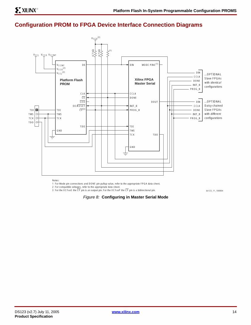
Platform Flash In-System Programmable Configuration PROMS
DS123 (v27) July 11 2005 wwwxilinxcom 15Product Specification
R
Figure 9 Configuring in Slave Serial Mode
Xilinx FPGASlave Serial
DIN
CCLK
DONE
INIT_B
PROG_B
TDI
TMS
TCK
GND
MODE PINS(1)
DOUT
TDO
VCCJ VCCO VCCINT
DIN
CCLK
DONE
INIT_B
PROG_B
DIN
CCLK
DONE
INIT_B
PROG_B
47
kΩ
47
kΩ (1)
VCCO(2)
OPTIONALDaisy-chainedSlave FPGAs with differentconfigurations
OPTIONALSlave FPGAs with identicalconfigurations
TDI
TMS
TCK
TDO
Notes1 For Mode pin connections and DONE pin pullup value refer to the appropriate FPGA data sheet2 For compatible voltages refer to the appropriate data sheet3 In Slave Serial mode the configuration interface can be clocked by an external oscillator or optionallymdashfor the XCFxxP Platform Flash PROM onlymdashthe CLKOUT signal can be used to drive the FPGAs configuration clock (CCLK) If the XCFxxP PROMs CLKOUT signal is used then it must be tied to a 47KΩ resistor pulled up to VCCO4 For the XCFxxS the CF pin is an output pin For the XCFxxP the CF pin is a bidirectional pin
Platform Flash PROM
VCCINT
VCCO(2)
VCCJ(2)
TDI
TMS
TCK
GND
D0
CLK(3)
CE
CEO
OERESET
CF(4)
TDO
ds123_12_070505
External (3)
Oscillator
Platform Flash In-System Programmable Configuration PROMS
DS123 (v27) July 11 2005 wwwxilinxcom 16Product Specification
R
Figure 10 Configuring Multiple Devices MasterSlave Serial Mode
Platform Flash PROM
First PROM(PROM 0)
VCCINT
VCCO(2)
VCCJ(2)
TDI
TMS
TCK
D0
CLK
CE
CEO
OERESET
CF(3)
TDO
Xilinx FPGAMaster Serial
DIN
CCLK
DONE
INIT_B
PROG_B
TDI
TMS
TCK
MODE PINS(1)
DOUT
TDO
VCCJ VCCO VCCINT
47
kΩ
47
kΩ (1)
VCCO(2)
TDI
TMS
TCK
TDO
Notes1 For Mode pin connections and DONE pin pullup value refer to the appropriate FPGA data sheet2 For compatible voltages refer to the appropriate data sheet3 For the XCFxxS the CF pin is an output pin For the XCFxxP the CF pin is a bidirectional pin
Xilinx FPGASlave Serial
DIN
CCLK
DONE
INIT_B
PROG_B
TDI
TMS
TCK
Platform Flash PROM
Cascaded PROM(PROM 1)
VCCINT
VCCO(2)
VCCJ(2)
TDI
TMS
TCK
D0
CLK
CE
CEO
OERESET
CF(3)
TDO
VCCJ VCCO VCCINT
MODE PINS(1)
TDO
ds123_13_100804
GND
GNDGND
GND
Platform Flash In-System Programmable Configuration PROMS
DS123 (v27) July 11 2005 wwwxilinxcom 17Product Specification
R
Figure 11 Configuring in Master SelectMAP Mode
XCFxxPPlatform Flash PROM
VCCINT
VCCO(2)
VCCJ(2)
TDI
TMS
TCK
GND
D[07]
CLK
CE
CEO
OERESET
CF(5)
BUSY(4)
TDO
Xilinx FPGAMaster SelectMAP
D[07]
CCLK
DONE
INIT_B
PROG_B
BUSY(4)
TDI
TMS
TCK
GND
MODE PINS(1)
RDWR_B
CS_B
TDO
VCCJ VCCO VCCINT
D[07]
CCLK
DONE
INIT_B
PROG_B
BUSY(4)
47
kΩ
47
kΩ (1)
VCCO(2)
OPTIONALSlave FPGAs with identicalconfigurations
TDI
TMS
TCK
TDO
Notes1 For Mode pin connections and DONE pin pullup value refer to the appropriate FPGA data sheet2 For compatible voltages refer to the appropriate data sheet3 CS_B (or CS) and RDWR_B (or WRITE) must be either driven Low or pulled down exernally One option is shown4 The BUSY pin is only available with the XCFxxP Platform Flash PROM and the connection is only required for high-frequency SelectMAP mode configuration For BUSY pin requirements refer to the appropriate FPGA data sheet5 For the XCFxxP the CF pin is a bidirectional pin
1KΩ
1KΩ
IO(3)
IO(3)
ds123_14_100804
Platform Flash In-System Programmable Configuration PROMS
DS123 (v27) July 11 2005 wwwxilinxcom 18Product Specification
R
Figure 12 Configuring in Slave SelectMAP Mode
XCFxxPPlatform Flash PROM
VCCINT
VCCO(2)
VCCJ(2)
TDI
TMS
TCK
GND
D[07]
CLK(5)
CE
CEO
OERESET
CF(6)
BUSY(4)
TDO
Xilinx FPGASlave SelectMAP
D[07]
CCLK
DONE
INIT_B
PROG_B
BUSY(4)
TDI
TMS
TCK
GND
MODE PINS(1)
RDWR_B
CS_B
TDO
VCCJ VCCO VCCINT
D[07]
CCLK
DONE
INIT_B
PROG_B
BUSY(4)
47
kΩ
47
kΩ (1)
VCCO(2)
OPTIONALSlave FPGAs with identicalconfigurations
TDI
TMS
TCK
TDO
Notes1 For Mode pin connections and DONE pin pullup value refer to the appropriate FPGA data sheet2 For compatible voltages refer to the appropriate data sheet3 CS_B (or CS) and RDWR_B (or WRITE) must be either driven Low or pulled down exernally One option is shown4 The BUSY pin is only available with the XCFxxP Platform Flash PROM and the connection is only required for high-frequency SelectMAP mode configuration For BUSY pin requirements refer to the appropriate FPGA data sheet5 In Slave SelectMAP mode the configuration interface can be clocked by an external oscillator or optionally the CLKOUT signal can be used to drive the FPGAs configuration clock (CCLK) If the XCFxxP PROMs CLKOUT signal is used then it must be tied to a 47KΩ resistor pulled up to VCCO6 For the XCFxxP the CF pin is a bidirectional pin
1KΩ
1KΩ
IO(3)
IO(3)
ds123_15_070505
External (5)
Oscillator
Platform Flash In-System Programmable Configuration PROMS
DS123 (v27) July 11 2005 wwwxilinxcom 19Product Specification
R
Figure 13 Configuring Multiple Devices with Identical Patterns in MasterSlave SelectMAP Mode
XCFxxPPlatform Flash PROM
First PROM(PROM 0)
VCCINT
VCCO(2)
VCCJ(2)
TDI
TMS
TCK
GND
D[07]
CLK
CE
CEO
OERESET
CF(5)
BUSY(4)
TDO
Xilinx FPGAMaster SelectMAP
D[07]
CCLK
DONE
INIT_B
PROG_B
BUSY(4)
TDI
TMS
TCK
GND
MODE PINS(1)
TDO
VCCJ VCCO VCCINT
47
kΩ
47
kΩ (1)
VCCO(2)
TDI
TMS
TCK
TDO
Notes1 For Mode pin connections and DONE pin pullup value refer to the appropriate FPGA data sheet2 For compatible voltages refer to the appropriate data sheet3 CS_B (or CS) and RDWR_B (or WRITE) must be either driven Low or pulled down exernally One option is shown4 The BUSY pin is only available with the XCFxxP Platform Flash PROM and the connection is only required for high-frequency SelectMAP mode configuration For BUSY pin requirements refer to the appropriate FPGA data sheet5 For the XCFxxP the CF pin is a bidirectional pin
Xilinx FPGASlave SelectMAP
D[07]
CCLK
DONE
INIT_B
PROG_B
BUSY(4)
TDI
TMS
TCK
GND
XCFxxPPlatform Flash PROM
Cascaded PROM(PROM 1)
VCCINT
VCCO(2)
VCCJ(2)
TDI
TMS
TCK
GND
D[07]
CLK
CE
CEO
OERESET
CF(5)
BUSY(4)
TDO
VCCJ VCCO VCCINT
MODE PINS(1)
TDO
ds123_16_100804
1KΩ1K
Ω
IO(3)
IO(3)
1KΩ1K
Ω
IO(3)
IO(3)RDWR_B
CS_B
RDWR_B
CS_B
Platform Flash In-System Programmable Configuration PROMS
DS123 (v27) July 11 2005 wwwxilinxcom 20Product Specification
R
Figure 14 Configuring Multiple Devices with Design Revisioning in Slave Serial Mode
XCFxxPPlatform Flash PROM
First PROM(PROM 0)
VCCINT
VCCO(2)
VCCJ(2)
TDI
TMS
TCK
EN_EXT_SEL
REV_SEL[10]
D0
CLK(3)
CE
CEO
OERESET
CF(4)
TDO
Xilinx FPGASlave Serial
DIN
CCLK
DONE
INIT_B
PROG_B
TDI
TMS
TCK
VCCJ VCCO VCCINT
47
kΩ
47
kΩ
(1)
VCCO(2)
TDI
TMS
TCK
TDO
1 For Mode pin connections and DONE pin pullup value refer to the appropriate FPGA data sheet
2 For compatible voltages refer to the appropriate data sheet3 In Slave Serial mode the configuration interface can be clocked by an external oscillator or optionally the CLKOUT signal can be used to drive the FPGAs configuration clock (CCLK) If the XCFxxP PROMs CLKOUT signal is used then it must be tied to a 47KΩ resistor pulled up to VCCO4 For the XCFxxP the CF pin is a bidirectional pin
XCFxxPPlatform Flash PROM
Cascaded PROM(PROM 1)
VCCINT
VCCO(2)
VCCJ(2)
TDI
TMS
TCK
EN_EXT_SEL
REV_SEL[10]
D0
CLK(3)
CE
CEO
OERESET
CF(4)
TDO
VCCJ VCCO VCCINT
ds123_17_070505
Design RevisionControl Logic
EN_EXT_SEL
REV_SEL[10]
DONE
CF PROG_B
Xilinx FPGASlave Serial
DIN
CCLK
DONE
INIT_B
PROG_B
TDI
TMS
TCK
MODE PINS(1)
TDO
GNDGND
GND
DOUT
MODE PINS(1)
GND
External (3)
Oscillator
Platform Flash In-System Programmable Configuration PROMS
DS123 (v27) July 11 2005 wwwxilinxcom 21Product Specification
R
Figure 15 Configuring Multiple Devices with Design Revisioning in Slave SelectMAP Mode
XCFxxPPlatform Flash PROM
First PROM(PROM 0)
VCCINT
VCCO(2)
VCCJ(2)
TDI
TMS
TCK
EN_EXT_SEL
REV_SEL[10]
GND
D[07]
CLK(5)
CE
CEO
OERESET
CF(6)
BUSY(4)
TDO
Xilinx FPGASlave SelectMAP
D[07]
CCLK
DONE
INIT_B
PROG_B
BUSY(4)
TDI
TMS
TCK
MODE PINS(1)
RDWR_B
CS_B
TDO
VCCJ VCCO VCCINT
47
kΩ
47
kΩ
(1)
VCCO(2)
TDI
TMS
TCK
TDO
Notes
1 For Mode pin connections and DONE pin pullup value refer to the appropriate FPGA data sheet
2 For compatible voltages refer to the appropriate data sheet
3 RDWR_B (or WRITE) must be either driven Low or pulled down exernally One option is shown
4 The BUSY pin is only available with the XCFxxP Platform Flash PROM and the connection is only required for high frequency SelectMAP mode configuration For BUSY pin requirements refer to the appropriate FPGA data sheet
5 In Slave SelectMAP mode the configuration interface can be clocked by an external oscillator or optionally the CLKOUT signal can be used to drive the FPGAs configuration clock (CCLK) If the XCFxxP PROMs CLKOUT signal is used then it must be tied to a 47KΩ resistor pulled up to VCCO6 For the XCFxxP the CF pin is a bidirectional pin
Xilinx FPGASlave SelectMAP
D[07]
CCLK
DONE
INIT_B
PROG_B
BUSY(4)
TDI
TMS
TCK
MODE PINS(1)
RDWR_B
CS_B
TDO
XCFxxPPlatform Flash PROM
Cascaded PROM(PROM 1)
VCCINT
VCCO(2)
VCCJ(2)
TDI
TMS
TCK
EN_EXT_SEL
REV_SEL[10]
GND
D[07]
CLK(5)
CE
CEO
OERESET
CF(6)
BUSY(4)
TDO
VCCJ VCCO VCCINT
1KΩ
IO(3)
1KΩ
IO(3)
EN_EXT_SEL
REV_SEL[10]
CF
DONE
PROG_B
CS_B[10]
Design
Revision
Control
Logic
GND GND
ds123_18_070505
External (5)
Oscillator
Platform Flash In-System Programmable Configuration PROMS
DS123 (v27) July 11 2005 wwwxilinxcom 22Product Specification
R
Reset and Power-On Reset ActivationAt power up the device requires the VCCINT power supplyto monotonically rise to the nominal operating voltage withinthe specified VCCINT rise time If the power supply cannotmeet this requirement then the device might not performpower-on reset properly During the power-up sequenceOERESET is held Low by the PROM Once the requiredsupplies have reached their respective POR (Power OnReset) thresholds the OERESET release is delayed (TOERminimum) to allow more margin for the power supplies tostabilize before initiating configuration The OERESET pinis connected to an external 47kΩ pull-up resistor and alsoto the target FPGAs INIT pin For systems utilizing slow-ris-ing power supplies an additional power monitoring circuitcan be used to delay the target configuration until the sys-tem power reaches minimum operating voltages by holdingthe OERESET pin Low When OERESET is released theFPGArsquos INIT pin is pulled High allowing the FPGAs config-uration sequence to begin If the power drops below the
power-down threshold (VCCPD) the PROM resets andOERESET is again held Low until the after the POR thresh-old is reached OERESET polarity is not programmableThese power-up requirements are shown graphically inFigure 16For a fully powered Platform Flash PROM a reset occurswhenever OERESET is asserted (Low) or CE is deas-serted (High) The address counter is reset CEO is drivenHigh and the remaining outputs are placed in a high-imped-ance stateNotes1 The XCFxxS PROM only requires VCCINT to rise above
its POR threshold before releasing OERESET 2 The XCFxxP PROM requires both VCCINT to rise above
its POR threshold and for VCCO to reach the recommended operating voltage level before releasing OERESET
IO Input Voltage Tolerance and Power Sequencing The IOs on each re-programmable Platform Flash PROMare fully 33V-tolerant This allows 3V CMOS signals to con-nect directly to the inputs without damage The core powersupply (VCCINT) JTAG pin power supply (VCCJ) outputpower supply (VCCO) and external 3V CMOS IO signalscan be applied in any order Additionally for the XCFxxS PROM only when VCCO is sup-plied at 25V or 33V and VCCINT is supplied at 33V theIOs are 5V-tolerant This allows 5V CMOS signals to con-nect directly to the inputs on a powered XCFxxS PROMwithout damage Failure to power the PROM correctly whilesupplying a 5V input signal may result in damage to theXCFxxS device
Standby ModeThe PROM enters a low-power standby mode whenever CEis deasserted (High) In standby mode the address counteris reset CEO is driven High and the remaining outputs areplaced in a high-impedance state regardless of the state ofthe OERESET input For the device to remain in thelow-power standby mode the JTAG pins TMS TDI andTDO must not be pulled Low and TCK must be stopped(High or Low)When using the FPGA DONE signal to drive the PROM CEpin High to reduce standby power after configuration anexternal pull-up resistor should be used Typically a 330Ωpull-up resistor is used but refer to the appropriate FPGAdata sheet for the recommended DONE pin pull-up value Ifthe DONE circuit is connected to an LED to indicate FPGA
Figure 16 Platform Flash PROM Power-Up Requirements
TOER
VCCINT
VCCPOR
VCCPD
200 micros ramp50 ms ramp
TOER TRST
TIME (ms)
A slow-ramping VCCINT supply may still be below the minimum operating voltage when OERESET is released In this case the configuration sequence must be delayed until both VCCINT and VCCO have reached their recommended operating conditions
Recommended Operating Range
Delay or RestartConfiguration
ds123_21_103103
Platform Flash In-System Programmable Configuration PROMS
DS123 (v27) July 11 2005 wwwxilinxcom 23Product Specification
R
configuration is complete and is also connected to thePROM CE pin to enable low-power standby mode then anexternal buffer should be used to drive the LED circuit to
ensure valid transitions on the PROMrsquos CE pin If low-powerstandby mode is not required for the PROM then the CE pinshould be connected to ground
DC Electrical CharacteristicsThis data sheet is a Preliminary data sheet The DC characteristics are based on characterization rather than simulationFurther characteristic changes are not expected
bullAbsolute Maximum Ratings page 24bullSupply Voltage Requirements for Power-On Reset and Power-Down page 24bullRecommended Operating Conditions page 25bullQuality and Reliability Characteristics page 25bullDC Characteristics Over Operating Conditions page 26
Table 9 Truth Table for XCFxxS PROM Control InputsControl Inputs
Internal Address
Outputs
OERESET CE DATA CEO ICC
High LowIf address lt TC(2) increment Active High Active
If address = TC(2) dont change High-Z Low Reduced
Low Low Held reset High-Z High Active
X(1) High Held reset High-Z High Standby
Notes 1 X = donrsquot care2 TC = Terminal Count = highest address value TC + 1 = address 0
Table 10 Truth Table for XCFxxP PROM Control InputsControl Inputs
Internal Address
Outputs
OERESET CE CF BUSY(5) DATA CEO CLKOUT ICC
High Low High Low
If address lt TC(2) and address lt EA(3) increment Active High Active Active
If address lt TC(2) and address = EA(3) dont change High-Z High High-Z Reduced
Else If address = TC(2) dont change High-Z Low High-Z Reduced
High Low High High Unchanged Active and Unchanged High Active Active
High Low uarr X(1) Reset(4) Active High Active Active
Low Low X X Held reset(4) High-Z High High-Z Active
X High X X Held reset(4) High-Z High High-Z Standby
Notes 1 X = donrsquot care2 TC = Terminal Count = highest address value TC + 1 = address 03 For the XCFxxP with Design Revisioning enabled EA = end address (last address in the selected design revision) 4 For the XCFxxP with Design Revisioning enabled Reset = address reset to the beginning address of the selected bank If Design Revisioning is not
enabled then Reset = address reset to address 05 The BUSY input is only enabled when the XCFxxP is programmed for parallel data output and decompression is not enabled
Platform Flash In-System Programmable Configuration PROMS
DS123 (v27) July 11 2005 wwwxilinxcom 24Product Specification
R
AC Electrical CharacteristicsThis data sheet is a Preliminary data sheet The AC characteristics are based on characterization rather than simulationFurther characteristic changes are not expected
bullAC Characteristics Over Operating Conditions page 28bullAC Characteristics Over Operating Conditions When Cascading page 32
Absolute Maximum Ratings
Supply Voltage Requirements for Power-On Reset and Power-Down
Symbol DescriptionXCF01S XCF02S
XCF04SXCF08P XCF16P
XCF32P Units
VCCINT Internal supply voltage relative to GND ndash05 to +40 ndash05 to +27 V
VCCO IO supply voltage relative to GND ndash05 to +40 ndash05 to +40 V
VCCJ JTAG IO supply voltage relative to GND ndash05 to +40 ndash05 to +40 V
VIN Input voltage with respect to GNDVCCO lt 25V ndash05 to +36 ndash05 to +36 V
VCCO ge 25V ndash05 to +55 ndash05 to +36 V
VTS Voltage applied to High-Z outputVCCO lt 25V ndash05 to +36 ndash05 to +36 V
VCCO ge 25V ndash05 to +55 ndash05 to +36 V
TSTG Storage temperature (ambient) ndash65 to +150 ndash65 to +150 degC
TJ Junction temperature +125 +125 degC
Notes 1 Maximum DC undershoot below GND must be limited to either 05V or 10 mA whichever is easier to achieve During transitions the device pins can
undershoot to ndash20V or overshoot to +70V provided this over- or undershoot lasts less then 10 ns and with the forcing current being limited to 200 mA
2 Stresses beyond those listed under Absolute Maximum Ratings might cause permanent damage to the device These are stress ratings only and functional operation of the device at these or any other conditions beyond those listed under Operating Conditions is not implied Exposure to Absolute Maximum Ratings conditions for extended periods of time adversely affects device reliability
3 For soldering guidelines see the information on Packaging and Thermal Characteristics at wwwxilinxcom
Symbol Description
XCF01S XCF02S XCF04S
XCF08P XCF16P XCF32P
UnitsMin Max Min Max
TVCC VCCINT rise time from 0V to nominal voltage(2) 02 50 02 50 ms
VCCPOR POR threshold for the VCCINT supply 1 - 05 - V
TOER OERESET release delay following POR(3) 05 3 05 30 ms
VCCPD Power-down threshold for VCCINT supply - 1 - 05 V
TRSTTime required to trigger a device reset when the VCCINT supply drops below the maximum VCCPD threshold 10 - 10 - ms
Notes 1 VCCINT VCCO and VCCJ supplies may be applied in any order2 At power up the device requires the VCCINT power supply to monotonically rise to the nominal operating voltage within the specified TVCC rise time
If the power supply cannot meet this requirement then the device might not perform power-on-reset properly See Figure 16 page 223 If the VCCINT and VCCO supplies do not reach their respective recommended operating conditions before the OERESET pin is released then the
configuration data from the PROM will not be available at the recommended threshold levels The configuration sequence must be delayed until both VCCINT and VCCO have reached their recommended operating conditions
huffman
XCF08P
huffman
XCF08P
Platform Flash In-System Programmable Configuration PROMS
DS123 (v27) July 11 2005 wwwxilinxcom 25Product Specification
R
Recommended Operating Conditions
Quality and Reliability Characteristics
Symbol Description
XCF01S XCF02S XCF04S XCF08P XCF16P XCF32P
UnitsMin Typ Max Min Typ MaxVCCINT Internal voltage supply 30 33 36 165 18 20 V
VCCOSupply voltage for output drivers
33V Operation 30 33 36 30 33 36 V
25V Operation 23 25 27 23 25 27 V
18V Operation 17 18 19 17 18 19 V
15V Operation - - - TBD 15 TBD V
VCCJSupply voltage for JTAG output drivers
33V Operation 30 33 36 30 33 36 V
25V Operation 23 25 27 23 25 27 V
VILLow-level input voltage
33V Operation 0 - 08 0 - 08 V
25V Operation 0 - 08 0 - 08 V
18V Operation - - 20 VCCO - - 20 VCCO V
15V Operation - - - 0 - TBD V
VIHHigh-level input voltage
33V Operation 20 - 55 20 - 36 V
25V Operation 17 - 55 17 - 36 V
18V Operation 70 VCCO - 36 70 VCCO - 36 V
15V Operation - - - TBD - 36 V
TIN Input signal transition time(1) - - 500 - - 500 ns
VO Output voltage 0 - VCCO 0 - VCCO V
TA Operating ambient temperature ndash40 - 85 ndash40 - 85 degC
Notes 1 Input signal transition time measured between 10 VCCO and 90 VCCO
Symbol Description Min Max Units
TDR Data retention 20 - Years
NPE Programerase cycles (Endurance) 20000 - Cycles
VESD Electrostatic discharge (ESD) 2000 - Volts
huffman
XCF08P
huffman
18
Platform Flash In-System Programmable Configuration PROMS
DS123 (v27) July 11 2005 wwwxilinxcom 26Product Specification
R
DC Characteristics Over Operating Conditions
Symbol Description
XCF01S XCF02S XCF04S
XCF08P XCF16P XCF32P
UnitsTest
Conditions Min MaxTest
Conditions Min Max
VOH
High-level output voltage for 33V outputs IOH = ndash4 mA 24 - IOH = ndash4 mA 24 - V
High-level output voltage for 25V outputs IOH = ndash500 microA VCCO ndash 04
- IOH = ndash500 microA VCCO ndash 04
- V
High-level output voltage for 18V outputs IOH = ndash50 microA VCCO ndash 04
- IOH = ndash50 microA VCCO ndash 04
- V
High-level output voltage for 15V outputs - - - IOH = TBD TBD - V
VOL
Low-level output voltage for 33V outputs IOL = 4 mA - 04 IOL = 4 mA - 04 V
Low-level output voltage for 25V outputs IOL = 500 microA - 04 IOL = 500 microA - 04 V
Low-level output voltage for 18V outputs IOL = 50 microA - 04 IOL = 50 microA - 04 V
Low-level output voltage for 15V outputs - - - IOL = TBD - TBD V
ICCINT Internal voltage supply current active mode 33 MHz - 10 33 MHz - 10 mA
ICCO(1)
Output driver supply current active serial mode 33 MHz - 10 33 MHz - 10 mA
Output driver supply current active parallel mode - - - 33 MHz - 40 mA
ICCJ JTAG supply current active mode Note (2) - 5 Note (2) - 5 mA
ICCINTS Internal voltage supply current standby mode Note (3) - 5 Note (3) - 5 mA
ICCOS Output driver supply current standby mode Note (3) - 1 Note (3) - 1 mA
ICCJS JTAG supply current standby mode Note (3) - 1 Note (3) - 1 mA
IILJ JTAG pins TMS TDI and TDO pull-up current VCCJ = maxVIN = GND - 100 VCCJ = max
VIN = GND - 100 microA
IIL Input leakage current
VCCINT = maxVCCO = maxVIN = GND or
VCCO
ndash10 10
VCCINT = maxVCCO = maxVIN = GND or
VCCO
ndash10 10 microA
IIH Input and output High-Z leakage current
VCCINT = maxVCCO = maxVIN = GND or
VCCO
ndash10 10
VCCINT = maxVCCO = maxVIN = GND or
VCCO
ndash10 10 microA
IILPSource current through internal pull-ups onEN_EXT_SEL REV_SEL0 REV_SEL1
- - -
VCCINT = maxVCCO = maxVIN = GND or
VCCO
- 100 microA
IIHP Sink current through internal pull-down on BUSY - - -
VCCINT = maxVCCO = maxVIN = GND or
VCCO
-100 - microA
huffman
XCF08P
Platform Flash In-System Programmable Configuration PROMS
DS123 (v27) July 11 2005 wwwxilinxcom 27Product Specification
R
CIN Input capacitance VIN = GNDf = 10 MHz - 8 VIN = GND
f = 10 MHz - 8 pF
COUT Output capacitance VIN = GNDf = 10 MHz - 14 VIN = GND
f = 10 MHz - 14 pF
Notes 1 Output driver supply current specification based on no load conditions2 TDITMSTCK non-static (active)3 CE High OE Low and TMSTDITCK static
Symbol Description
XCF01S XCF02S XCF04S
XCF08P XCF16P XCF32P
UnitsTest
Conditions Min MaxTest
Conditions Min Max
huffman
XCF08P
Platform Flash In-System Programmable Configuration PROMS
DS123 (v27) July 11 2005 wwwxilinxcom 28Product Specification
R
AC Characteristics Over Operating Conditions
Symbol Description
XCF01S XCF02S XCF04S
XCF08P XCF16P XCF32P
UnitsMin Max Min Max
TOEOERESET to data delay(6) when VCCO = 33V or 25V - 10 - 25 ns
OERESET to data delay(6) when VCCO = 18V - 30 - 25 ns
TCECE to data delay(5) when VCCO = 33V or 25V - 15 - 25 ns
CE to data delay(5) when VCCO = 18V - 30 - 25 ns
TCACCLK to data delay(7) when VCCO = 33V or 25V - 15 - 25 ns
CLK to data delay(7) when VCCO = 18V - 30 - 25 ns
TOH
Data hold from CE OERESET or CLKwhen VCCO = 33V or 25V 0 - 5 - ns
Data hold from CE OERESET or CLKwhen VCCO = 18V 0 - 5 - ns
TDF
CE or OERESET to data float delay(2)
when VCCO = 33V or 25V - 25 - 45 ns
CE or OERESET to data float delay(2)
when VCCO = 18V - 30 - 45 ns
TCYC
Clock period(7) (serial mode) when VCCO = 33V or 25V 30 - 25 - ns
Clock period(7) (serial mode) when VCCO = 18V 67 - 25 - ns
Clock period(7) (parallel mode) when VCCO = 33V or 25V - - 30 - ns
Clock period(7) (parallel mode) when VCCO = 18V - - 30 - ns
CE
OERESET
CLK
CLKOUT(optional)
BUSY(optional)
DATA
TCE
TLC THC
TSCE
TOE TCAC
THCE
THOE
TCYC
TOH
TDFTOH
THBTSBTOEC
TCEC
TCLKO
TCOH
TCDD
CF
EN_EXT_SEL
REV_SEL[10]
TSXT THXT
TSRV THRV
ds123_22_110403
huffman
XCF08P
Platform Flash In-System Programmable Configuration PROMS
DS123 (v27) July 11 2005 wwwxilinxcom 29Product Specification
R
TLCCLK Low time(3) when VCCO = 33V or 25V 10 - 12 - ns
CLK Low time(3) when VCCO = 18V 15 - 12 - ns
THCCLK High time(3) when VCCO = 33V or 25V 10 - 12 - ns
CLK High time(3) when VCCO = 18V 15 - 12 - ns
TSCE
CE setup time to CLK (guarantees proper counting)(3)
when VCCO = 33V or 25V 20 - 30 - ns
CE setup time to CLK (guarantees proper counting)(3)
when VCCO = 18V 30 30 - ns
THCE
CE hold time (guarantees counters are reset)(5)
when VCCO = 33V or 25V 250 - 2000 - ns
CE hold time (guarantees counters are reset)(5)
when VCCO = 18V 250 - 2000 - ns
THOE
OERESET hold time (guarantees counters are reset)(6)
when VCCO = 33V or 25V 250 - 2000 - ns
OERESET hold time (guarantees counters are reset)(6)
when VCCO = 18V 250 - 2000 - ns
TSBBUSY setup time to CLK when VCCO = 33V or 25V - - 12 - ns
BUSY setup time to CLK when VCCO = 18V - - 12 - ns
THBBUSY hold time to CLK when VCCO = 33V or 25V - - 8 - ns
BUSY hold time to CLK when VCCO = 18V - - 8 - ns
TCLKO
CLK input to CLKOUT output delay when VCCO = 33V or 25V - - - 35 ns
CLK input to CLKOUT output delay when VCCO = 18V - - - 35 ns
CLK input to CLKOUT output delay when VCCO = 33V or 25V with decompression(12) - - - 35 ns
CLK input to CLKOUT output delay when VCCO = 18V with decompression(12) - - - 35 ns
TCEC
CE to CLKOUT delay(8) with CLKOUT sourced from internal oscillator when VCCO = 33V or 25V - - 0 1 micros
CE to CLKOUT delay(8) with CLKOUT sourced from internal oscillator when VCCO = 18V - - 0 1 micros
CE to CLKOUT delay(8) with CLKOUT sourced from external CLK input when VCCO = 33V or 25V - - 0 2 CLK
cycles -
CE to CLKOUT delay(8) with CLKOUT sourced from external CLK input when VCCO = 18V - - 0 2 CLK
cycles -
TOEC
OERESET to CLKOUT delay(8) with CLKOUT sourced from internal oscillator when VCCO = 33V or 25V - - 0 1 micros
OERESET to CLKOUT delay(8) with CLKOUT sourced from internal oscillator when VCCO = 18V - - 0 1 micros
OERESET to CLKOUT delay(8) with CLKOUT sourced from external CLK input when VCCO = 33V or 25V 0 2 CLK
cycles -
OERESET to CLKOUT delay(8) with CLKOUT sourced from external CLK input when VCCO = 18V 0 2 CLK
cycles -
Symbol Description
XCF01S XCF02S XCF04S
XCF08P XCF16P XCF32P
UnitsMin Max Min Max
huffman
XCF08P
Platform Flash In-System Programmable Configuration PROMS
DS123 (v27) July 11 2005 wwwxilinxcom 30Product Specification
R
TCDDCLKOUT to data delay when VCCO = 33V or 25V(9) - - - 22 ns
CLKOUT to data delay when VCCO = 18V(9) - - - 22 ns
TDDC
Data setup time to CLKOUT when VCCO = 33V or 25V with decompression(9)(12) - - 5 ns
Data setup time to CLKOUT when VCCO = 18V with decompression(9)(12) - - 5 ns
TCOH
Data hold from CLKOUT when VCCO = 33V or 25V - - 3 - ns
Data hold from CLKOUT when VCCO = 18V - - 3 - ns
Data hold from CLKOUT when VCCO = 33V or 25V with decompression(12) - - 3 - ns
Data hold from CLKOUT when VCCO = 18V with decompression(12) - - 3 - ns
TSXT
EN_EXT_SEL setup time to CF (rising edge)when VCCO = 33V or 25V - - 300 - ns
EN_EXT_SEL setup time to CF (rising edge)when VCCO = 18V - - 300 - ns
THXT
EN_EXT_SEL hold time from CF (rising edge)when VCCO = 33V or 25V - - 300 - ns
EN_EXT_SEL hold time from CF (rising edge)when VCCO = 18V - - 300 - ns
TSRV
REV_SEL setup time to CF (rising edge)when VCCO = 33V or 25V - - 300 - ns
REV_SEL setup time to CF (rising edge)when VCCO = 18V - - 300 - ns
THRV
REV_SEL hold time from CF (rising edge)when VCCO = 33V or 25V - - 300 - ns
REV_SEL hold time from CF (rising edge)when VCCO = 18V - - 300 - ns
FF
CLKOUT default (fast) frequency(10) - - 25 50 MHz
CLKOUT default (fast) frequency with decompression(12) - - 125 25 MHz
Symbol Description
XCF01S XCF02S XCF04S
XCF08P XCF16P XCF32P
UnitsMin Max Min Max
huffman
XCF08P
Platform Flash In-System Programmable Configuration PROMS
DS123 (v27) July 11 2005 wwwxilinxcom 31Product Specification
R
FS
CLKOUT alternate (slower) frequency(11) - - 125 25 MHz
CLKOUT alternate (slower) frequency with decompression(12) - - 6 125 MHz
Notes 1 AC test load = 50 pF for XCF01SXCF02SXCF04S 30 pF for XCF08PXCF16PXCF32P2 Float delays are measured with 5 pF AC loads Transition is measured at plusmn200 mV from steady-state active levels3 Guaranteed by design not tested4 All AC parameters are measured with VIL = 00V and VIH = 30V5 If THCE High lt 2 micros TCE = 2 micros6 If THOE Low lt 2 micros TOE = 2 micros7 This is the minimum possible TCYC Actual TCYC = TCAC + FPGA Data setup time
Example With the XCF32P in serial mode with VCCO at 33V if FPGA Data setup time = 15 ns then the actual TCYC = 25 ns +15 ns = 40 ns8 The delay before the enabled CLKOUT signal begins clocking data out of the device is dependent on the clocking configuration The delay before
CLKOUT is enabled will increase if decompression is enabled 9 Slower CLK frequency option may be required to meet the FPGA data sheet setup time10 Typical CLKOUT default (fast) period = 25 ns (40 MHz)11 Typical CLKOUT alternate (slower) period = 50 ns (20 MHz)12 When decompression is enabled the CLKOUT signal becomes a controlled clock output When decompressed data is available CLKOUT will toggle
at frac12 the source clock frequency (either frac12 the selected internal clock frequency or frac12 the external CLK input frequency) When decompressed data is not available the CLKOUT pin is parked High If CLKOUT is used then it must be pulled High externally using a 47kΩ pull-up to VCCO
Symbol Description
XCF01S XCF02S XCF04S
XCF08P XCF16P XCF32P
UnitsMin Max Min Max
huffman
XCF08P
huffman
XCF08P
Platform Flash In-System Programmable Configuration PROMS
DS123 (v27) July 11 2005 wwwxilinxcom 32Product Specification
R
AC Characteristics Over Operating Conditions When Cascading
Symbol Description
XCF01S XCF02S XCF04S
XCF08P XCF16P XCF32P
UnitsMin Max Min Max
TCDF
CLK to output float delay(23) when VCCO = 25V or 33V - 25 - 20 ns
CLK to output float delay(23) when VCCO = 18V - 35 - 20 ns
TOCKCLK to CEO delay(35) when VCCO = 25V or 33V - 20 - 20 ns
CLK to CEO delay(35) when VCCO = 18V - 35 - 20 ns
TOCECE to CEO delay(36) when VCCO = 25V or 33V - 20 - 80 ns
CE to CEO delay(36) when VCCO = 18V - 35 - 80 ns
TOOEOERESET to CEO delay(3) when VCCO = 25V or 33V - 20 - 80 ns
OERESET to CEO delay(3) when VCCO = 18V - 35 - 80 ns
TCOCECLKOUT to CEO delay when VCCO = 25V or 33V - - - 20 ns
CLKOUT to CEO delay when VCCO = 18V - - - 20 ns
TCODF
CLKOUT to output float delay when VCCO = 25V or 33V - - - 25 ns
CLKOUT to output float delay when VCCO = 18V - - - 25 ns
Notes 1 AC test load = 50 pF for XCF01SXCF02SXCF04S 30 pF for XCF08PXCF16PXCF32P2 Float delays are measured with 5 pF AC loads Transition is measured at plusmn200 mV from steady state active levels3 Guaranteed by design not tested4 All AC parameters are measured with VIL = 00V and VIH = 30V5 For cascaded PROMs if the FPGArsquos dual-purpose configuration data pins are set to persist as configuration pins the minimum period is increased
based on the CLK to CEO and CE to data propagation delays- TCYC minimum = TOCK + TCE + FPGA Data setup time- TCAC maximum = TOCK + TCE
6 For cascaded PROMs if the FPGArsquos dual-purpose configuration data pins become general IO pins after configuration to allow for the disable to propagate to the cascaded PROMs and to avoid contention on the data lines following configuration the minimum period is increased based on the CE to CEO and CE to data propagation delays- TCYC minimum = TOCE + TCE - TCAC maximum = TOCK + TCE
OERESET
CE
CLK
CLKOUT(optional)
DATA
CEO
TOCETOOE
First BitLast Bit
TCDFTCODF
TOCK TCOCE
ds123_23_102203
huffman
XCF08P
huffman
XCF08P
Platform Flash In-System Programmable Configuration PROMS
DS123 (v27) July 11 2005 wwwxilinxcom 33Product Specification
R
Pinouts and Pin DescriptionsThe XCFxxS Platform Flash PROM is available in the VO20 and VOG20 packages The XCFxxP Platform Flash PROM isavailable in the VO48 VOG48 FS48 and FSG48 packages This section includes
bull Table 11 XCFxxS Pin Names and Descriptions page 33bull Figure 17 VO20VOG20 Pinout Diagram (Top View) with Pin Names page 34bull Table 12 XCFxxP Pin Names and Descriptions page 35bull Figure 18 VO48VOG48 Pinout Diagram (Top View) with Pin Names page 36bull Table 13 FS48FSG48 Pin NumberName Reference page 38bull Figure 19 FS48FSG48 Pinout Diagram (Top View) page 38
Notes 1 VO20VOG20 denotes a 20-pin (TSSOP) Plastic Thin Shrink Small Outline Package 2 VO48VOG48 denotes a 48-pin (TSOP) Plastic Thin Small Outline Package3 FS48FSG48 denotes a 48-pin (TFBGA) Plastic Thin Fine Pitch Ball Grid Array (08 mm pitch)
XCFxxS Pinouts and Pin DescriptionsTable 11 provides a list of the pin names and descriptions for the XCFxxS 20-pin VO20VOG20 package
Table 11 XCFxxS Pin Names and Descriptions
Pin NameBoundary
Scan OrderBoundary
Scan Function Pin Description20-pin TSSOP (VO20VOG20)
D04 Data Out D0 is the DATA output pin to provide data for configuring an
FPGA in serial mode The D0 output is set to a high-impedance state during ISPEN (when not clamped)
13 Output Enable
CLK 0 Data InConfiguration Clock Input Each rising edge on the CLK input increments the internal address counter if the CLK input is selected CE is Low and OERESET is High
3
OERESET
20 Data In Output EnableReset (Open-Drain IO) When Low this input holds the address counter reset and the DATA output is in a high-impedance state This is a bidirectional open-drain pin that is held Low while the PROM is reset Polarity is not programmable
819 Data Out
18 Output Enable
CE 15 Data InChip Enable Input When CE is High the device is put into low-power standby mode the address counter is reset and the DATA pins are put in a high-impedance state
10
CF22 Data Out Configuration Pulse (Open-Drain Output) Allows JTAG
CONFIG instruction to initiate FPGA configuration without powering down FPGA This is an open-drain output that is pulsed Low by the JTAG CONFIG command
721 Output Enable
CEO
12 Data OutChip Enable Output Chip Enable Output (CEO) is connected to the CE input of the next PROM in the chain This output is Low when CE is Low and OERESET input is High AND the internal address counter has been incremented beyond its Terminal Count (TC) value CEO returns to High when OERESET goes Low or CE goes High
13
11 Output Enable
TMS Mode Select
JTAG Mode Select Input The state of TMS on the rising edge of TCK determines the state transitions at the Test Access Port (TAP) controller TMS has an internal 50KΩ resistive pull-up to VCCJ to provide a logic 1 to the device if the pin is not driven
5
TCK ClockJTAG Clock Input This pin is the JTAG test clock It sequences the TAP controller and all the JTAG test and programming electronics
6
Platform Flash In-System Programmable Configuration PROMS
DS123 (v27) July 11 2005 wwwxilinxcom 34Product Specification
R
XCFxxS Pinout Diagram
TDI Data In
JTAG Serial Data Input This pin is the serial input to all JTAG instruction and data registers TDI has an internal 50KΩ resistive pull-up to VCCJ to provide a logic 1 to the device if the pin is not driven
4
TDO Data Out
JTAG Serial Data Output This pin is the serial output for all JTAG instruction and data registers TDO has an internal 50KΩ resistive pull-up to VCCJ to provide a logic 1 to the system if the pin is not driven
17
VCCINT +33V Supply Positive 33V supply voltage for internal logic 18
VCCO+33V 25V or 18V IO Supply Positive 33V 25V or 18V supply voltage connected to the output voltage drivers and input buffers
19
VCCJ+33V or 25V JTAG IO Supply Positive 33V 25V or 18V supply voltage connected to the TDO output voltage driver and TCK TMS and TDI input buffers
20
GND Ground 11
DNC Do not connect (These pins must be left unconnected) 2 9 12 14 15 16
Figure 17 VO20VOG20 Pinout Diagram (Top View) with Pin Names
Table 11 XCFxxS Pin Names and Descriptions (Continued)
Pin NameBoundary
Scan OrderBoundary
Scan Function Pin Description20-pin TSSOP (VO20VOG20)
VO20VOG20Top View
ds123_02_071304
1
2
3
4
5
6
7
8
9
10
20
19
18
17
16
15
14
13
12
11
D0
(DNC)
CLK
TDI
TMS
TCK
CF
OERESET
(DNC)
CE
VCCJ
VCCO
VCCINT
TDO
(DNC)
(DNC)
CEO
(DNC)
GND
(DNC)
Platform Flash In-System Programmable Configuration PROMS
DS123 (v27) July 11 2005 wwwxilinxcom 35Product Specification
R
XCFxxP Pinouts and Pin DescriptionsTable 12 provides a list of the pin names and descriptions for the XCFxxP 48-pin VO48VOG48 and 48-pin FS48FSG48packages
Table 12 XCFxxP Pin Names and Descriptions
Pin Name
Boundary Scan Order
Boundary Scan
Function Pin Description
48-pin TSOP (VO48VOG48)
48-pin TFBGA (FS48FSG48)
D028 Data Out
D0 is the DATA output pin to provide data for configuring an FPGA in serial mode D0-D7 are the DATA output pins to provide parallel data for configuring a Xilinx FPGA in SelectMap (parallel) mode The D0 output is set to a high-impedance state during ISPEN (when not clamped)The D1-D7 outputs are set to a high-impedance state during ISPEN (when not clamped) and when serial mode is selected for configuration The D1-D7 pins can be left unconnected when the PROM is used in serial mode
28 H627 Output Enable
D126 Data Out
29 H525 Output Enable
D224 Data Out
32 E523 Output Enable
D322 Data Out
33 D521 Output Enable
D420 Data Out
43 C519 Output Enable
D518 Data Out
44 B517 Output Enable
D616 Data Out
47 A515 Output Enable
D714 Data Out
48 A613 Output Enable
CLK 01 Data In
Configuration Clock Input An internal programmable control bit selects between the internal oscillator and the CLK input pin as the clock source to control the configuration sequence Each rising edge on the CLK input increments the internal address counter if the CLK input is selected CE is Low OERESET is High BUSY is Low (parallel mode only) and CF is High
12 B3
OERESET
04 Data In Output EnableReset (Open-Drain IO)When Low this input holds the address counter reset and the DATA and CLKOUT outputs are placed in a high-impedance state This is a bidirectional open-drain pin that is held Low while the PROM is reset Polarity is not programmable
11 A303 Data Out
02 Output Enable
CE 00 Data In
Chip Enable Input When CE is High the device is put into low-power standby mode the address counter is reset and the DATA and CLKOUT outputs are placed in a high-impedance state
13 B4
CF
11 Data InConfiguration Pulse (Open-Drain IO) As an output this pin allows the JTAG CONFIG instruction to initiate FPGA configuration without powering down the FPGA This is an open-drain signal that is pulsed Low by the JTAG CONFIG command As an input on the rising edge of CF the current design revision selection is sampled and the internal address counter is reset to the start address for the selected revision If unused the CF pin should be pulled High using an external 47KΩ pull-up to VCCO
6 D110 Data Out
09 Output Enable
Platform Flash In-System Programmable Configuration PROMS
DS123 (v27) July 11 2005 wwwxilinxcom 36Product Specification
R
CEO
06 Data OutChip Enable Output Chip Enable Output (CEO) is connected to the CE input of the next PROM in the chain This output is Low when CE is Low and OERESET input is High AND the internal address counter has been incremented beyond its Terminal Count (TC) value CEO returns to High when OERESET goes Low or CE goes High
10 D2
05 Output Enable
EN_EXT_SEL 31 Data In
Enable External Selection Input When this pin is Low design revision selection is controlled by the Revision Select pins When this pin is High design revision selection is controlled by the internal programmable Revision Select control bits EN_EXT_SEL has an internal 50KΩ resistive pull-up to VCCO to provide a logic 1 to the device if the pin is not driven
25 H4
REV_SEL0 30 Data InRevision Select[10] Inputs When the EN_EXT_SEL is Low the Revision Select pins are used to select the design revision to be enabled overriding the internal programmable Revision Select control bits The Revision Select[10] inputs have an internal 50KΩ resistive pull-up to VCCO to provide a logic 1 to the device if the pins are not driven
26 G3
REV_SEL1 29 Data In 27 G4
BUSY 12 Data In
Busy Input The BUSY input is enabled when parallel mode is selected for configuration When BUSY is High the internal address counter stops incrementing and the current data remains on the data pins On the first rising edge of CLK after BUSY transitions from High to Low the data for the next address is driven on the data pins When serial mode or decompression is enabled during device programming the BUSY input is disabled BUSY has an internal 50KΩ resistive pull-down to GND to provide a logic 0 to the device if the pin is not driven
5 C1
CLKOUT
08 Data Out
Configuration Clock Output An internal Programmable control bit enables the CLKOUT signal which is sourced from either the internal oscillator or the CLK input pin Each rising edge of the selected clock source increments the internal address counter if data is available CE is Low and OERESET is High Output data is available on the rising edge of CLKOUT CLKOUT is disabled if CE is High or OERESET is Low If decompression is enabled CLKOUT is parked High when decompressed data is not ready When CLKOUT is disabled the CLKOUT pin is put into a high-Z state If CLKOUT is used then it must be pulled High externally using a 47KΩ pull-up to VCCO
9 C2
07 Output Enable
TMS Mode Select
JTAG Mode Select Input The state of TMS on the rising edge of TCK determines the state transitions at the Test Access Port (TAP) controller TMS has an internal 50KΩ resistive pull-up to VCCJ to provide a logic 1 to the device if the pin is not driven
21 E2
TCK ClockJTAG Clock Input This pin is the JTAG test clock It sequences the TAP controller and all the JTAG test and programming electronics
20 H3
TDI Data In
JTAG Serial Data Input This pin is the serial input to all JTAG instruction and data registers TDI has an internal 50KΩ resistive pull-up to VCCJ to provide a logic 1 to the device if the pin is not driven
19 G1
Table 12 XCFxxP Pin Names and Descriptions (Continued)
Pin Name
Boundary Scan Order
Boundary Scan
Function Pin Description
48-pin TSOP (VO48VOG48)
48-pin TFBGA (FS48FSG48)
Platform Flash In-System Programmable Configuration PROMS
DS123 (v27) July 11 2005 wwwxilinxcom 37Product Specification
R
XCFxxP Pinout Diagrams
Figure 18 VO48VOG48 Pinout Diagram (Top View) with Pin Names
TDO Data Out
JTAG Serial Data Output This pin is the serial output for all JTAG instruction and data registers TDO has an internal 50KΩ resistive pull-up to VCCJ to provide a logic 1 to the system if the pin is not driven
22 E6
VCCINT +18V Supply Positive 18V supply voltage for internal logic 4 15 34
B1 E1 G6
VCCO+33V 25V or 18V IO Supply Positive 33V 25V or 18V supply voltage connected to the output voltage drivers and input buffers
8 30 38 45
B2 C6 D6 G5
VCCJ+33V or 25V JTAG IO Supply Positive 33V 25V or 18V supply voltage connected to the TDO output voltage driver and TCK TMS and TDI input buffers
24 H2
GND Ground2 7
17 23 31 36
46
A1 A2 B6 F1 F5 F6
H1
DNC Do Not Connect (These pins must be left unconnected)
1 3 14 16 18 35 37 39 40 41
42
A4 C3 C4 D3 D4 E3 E4 F2 F3 F4
G2
Table 12 XCFxxP Pin Names and Descriptions (Continued)
Pin Name
Boundary Scan Order
Boundary Scan
Function Pin Description
48-pin TSOP (VO48VOG48)
48-pin TFBGA (FS48FSG48)
123456789101112131415161718192021222324
484746454443424140393837363534333231302928272625
VO48VOG48Top View
DNCGNDDNC
VCCINTBUSY
CFGND
VCCOCLKOUT
CEOOERESET
CLKCE
DNCVCCINT
DNCGNDDNCTDI
TCKTMSTDOGND
D7D6GNDVCCOD5D4DNCDNCDNCDNCVCCODNCGNDDNCVCCINTD3D2GNDVCCOD1D0REV_SEL1REV_SEL0EN_EXT_SELVCCJ
Platform Flash In-System Programmable Configuration PROMS
DS123 (v27) July 11 2005 wwwxilinxcom 38Product Specification
R
Table 13 FS48FSG48 Pin NumberName ReferencePin
Number Pin NamePin
Number Pin NameA1 GND E1 VCCINT
A2 GND E2 TMS
A3 OERESET E3 DNC
A4 DNC E4 DNC
A5 D6 E5 D2
A6 D7 E6 TDO
B1 VCCINT F1 GND
B2 VCCO F2 DNC
B3 CLK F3 DNC
B4 CE F4 DNC
B5 D5 F5 GND
B6 GND F6 GND
C1 BUSY G1 TDI
C2 CLKOUT G2 DNC
C3 DNC G3 REV_SEL0
C4 DNC G4 REV_SEL1
C5 D4 G5 VCCO
C6 VCCO G6 VCCINT
D1 CF H1 GND
D2 CEO H2 VCCJ
D3 DNC H3 TCK
D4 DNC H4 EN_EXT_SEL
D5 D3 H5 D1
D6 VCCO H6 D0
Table 13 FS48FSG48 Pin NumberName ReferencePin
Number Pin NamePin
Number Pin Name
1 2 3 4 5 6
ds121_01_071604
A
B
C
D
E
F
G
H
FS48FSG48Top View
Platform Flash In-System Programmable Configuration PROMS
DS123 (v27) July 11 2005 wwwxilinxcom 39Product Specification
R
Ordering Information
Valid Ordering Combinations
Marking Information
XCF01SVO20 C XCF08PVO48 C XCF08PFS48 C XCF01SVOG20 C XCF08PVOG48 C XCF08PFSG48 C
XCF02SVO20 C XCF16PVO48 C XCF16PFS48 C XCF02SVOG20 C XCF16PVOG48 C XCF16PFSG48 C
XCF04SVO20 C XCF32PVO48 C XCF32PFS48 C XCF04SVOG20 C XCF32PVOG48 C XCF32PFSG48 C
XCF04S VO20 C
Operating RangeProcessingC = (TA = ndash40degC to +85degC)Package Type
VO20 = 20-pin TSSOP PackageVOG20 = 20-pin TSSOP Package Pb-free
Device NumberXCF01SXCF02SXCF04S
XCF32P FS48 C
Operating RangeProcessingC = (TA = ndash40degC to +85degC)Package Type
VO48 = 48-pin TSOP PackageVOG48 = 48-pin TSOP Package Pb-freeFS48 = 48-pin TFBGA PackageFSG48 = 48-pin TFBGA Package Pb-free
Device NumberXCF08PXCF16PXCF32P
XCF04S-V
Operating RangeProcessingC = (TA = ndash40degC to +85degC)Package Type
V = 20-pin TSSOP Package (VO20)VG = 20-pin TSSOP Package Pb-free (VOG20)VO48 = 48-pin TSOP Package (VO48)VOG48 = 48-pin TSOP Package Pb-free (VOG48)F48 = 48-pin TFBGA Package (FS48)FG48 = 48-pin TFBGA Package Pb-free (FSG48)
Device NumberXCF01SXCF02SXCF04SXCF08PXCF16PXCF32P
huffman
XCF08PFS48 C
huffman
XCF08P
huffman
XCF08P
Platform Flash In-System Programmable Configuration PROMS
DS123 (v27) July 11 2005 wwwxilinxcom 40Product Specification
R
Revision HistoryThe following table shows the revision history for this document
Date Version Revision
042903 10 Xilinx Initial Release
060303 11 Made edits to all pages
110503 20 Major revision
111803 21 Pinout corrections as followsbull Table 12
- For VO48 package removed 38 from VCCINT and added it to VCCO- For FS48 package removed pin D6 from VCCINT and added it to VCCO
bull Table 13 (FS48 package) - For pin D6 changed name from VCCINT to VCCO- For pin A4 changed name from GND to DNC
bull Figure 18 (VO48 package) For pin 38 changed name from VCCINT to VCCO
121503 22 bull Added specification (47kΩ) for recommended pull-up resistor on OERESET pin to section Reset and Power-On Reset Activation page 22
bull Added paragraph to section Standby Mode page 22 concerning use of a pull-up resistor andor buffer on the DONE pin
050704 23 bull Section Features page 1 Added package styles and 33 MHz configuration speed limit to itemized features
bull Section Description page 1 and following Added state conditions for CF and BUSY to the descriptive text
bull Table 2 page 3 Updated Virtex-II configuration bitstream sizesbull Section Design Revisioning page 9 Rewrittenbull Section PROM to FPGA Configuration Mode and Connections Summary
page 10 and following five instances Added instruction to tie CF High if it is not tied to the FPGArsquos PROG_B (PROGRAM) input
bull Figure 8 page 14 through Figure 15 page 21 Added footnote indicating the directionality of the CF pin in each configuration
bull Section IO Input Voltage Tolerance and Power Sequencing page 22 Rewrittenbull Table 10 page 23 Added CF column to truth table and added an additional row to
document the Low state of CFbull Section Absolute Maximum Ratings page 24 Revised VIN and VTS for rsquoPrsquo
devices bull Section Supply Voltage Requirements for Power-On Reset and Power-Down
page 24- Revised footnote callout number on TOER from Footnote (4) to Footnote (3)- Added Footnote (2) callout to TVCC
bull Section Recommended Operating Conditions page 25 - Added Typical (Typ) parameter columns and parameters for VCCINT and
VCCOVCCJ- Added 15V operation parameter row to VIL and VIH rsquoPrsquo devices- Revised VIH Min 25V operation from 20V to 17V- Added parameter row TIN and Max parameters
bull (Continued on next page)
Platform Flash In-System Programmable Configuration PROMS
DS123 (v27) July 11 2005 wwwxilinxcom 41Product Specification
R
050704(contrsquod)
23(contrsquod)
bull Section DC Characteristics Over Operating Conditions page 26 - Added parameter row and parameters for parallel configuration mode rsquoPrsquo
devices to ICCO- Added Footnote (1) and Footnote (2) with callouts in the Test Conditions column
for ICCJ ICCINTS ICCOS and ICCJS to define active and standby mode requirements
bull Section AC Characteristics Over Operating Conditions page 28 - Corrected description for second TCAC parameter line to show parameters for
18V VCCO- Revised Footnote (7) to indicate VCCO = 33V- Applied Footnote (7) to second TCYC parameter line
bull Section AC Characteristics Over Operating Conditions When Cascading page 32 Revised Footnote (5)TCYC Min and TCAC Min formulas
bull Table 12 page 35 - Added additional state conditions to CLK description- Added function of resetting the internal address counter to CF description
072004 24 bull Added Pb-free package options VOG20 FSG48 and VOG48bull Figure 8 page 14 and Figure 9 page 15 Corrected connection name for FPGA
DOUT (OPTIONAL Daisy-chained Slave FPGAs with different configurations) from DOUT to DIN
bull Section Absolute Maximum Ratings page 24 Removed parameter TSOL from table (TSOL information can be found in Package User Guide)
bull Table 2 page 3 Removed reference to XC2VP125 FPGA
101804 25 bull Table 1 page 1 Broke out VCCO VCCJ into two separate columnsbull Table 7 page 7 Added clarification of ID code die revision bitsbull Table 8 page 8 Deleted TCKMIN2 (bypass mode) and renamed TCKMIN1 to TCKMINbull Table Recommended Operating Conditions page 25 Separated VCCO and VCCJ
parametersbull Table DC Characteristics Over Operating Conditions page 26
- Added most parameter values for XCF08P XCF16P XCF32P devices- Added Footnote (1) to ICCO specifying no-load conditions
bull Table AC Characteristics Over Operating Conditions page 28 - Added most parameter values for XCF08P XCF16P XCF32P devices- Expanded Footnote (1) to include XCF08P XCF16P XCF32P devices- Added Footnote (8) through (11) relating to CLKOUT conditions for various
parameters- Added rows to TCYC specifying parameters for parallel mode- Added rows specifying parameters with decompression for TCLKO TCOH TFF
TSF- Added TDDC (setup time with decompression)
bull Table AC Characteristics Over Operating Conditions When Cascading page 32 - Added most parameter values for XCF08P XCF16P XCF32P devices- Separated Footnote (5) into Footnotes (5) and (6) to specify different
derivations of TCYC depending on whether dual-purpose configuration pins persist as configuration pins or become general IO pins after configuration
huffman
XCF08P
huffman
XCF08P
huffman
XCF08P
huffman
XCF08P
Platform Flash In-System Programmable Configuration PROMS
DS123 (v27) July 11 2005 wwwxilinxcom 42Product Specification
R
031405 26 bull Added Virtex-4 LXFXSX configuration data to Table 2 bull Corrected Virtex-II configuration data in Table 2bull Corrected Virtex-II Pro configuration data in Table 2bull Added Spartan-3L configuration data to Table 2bull Added Spartan-3E configuration data to Table 2bull Paragraph added to FPGA Master SelectMAP (Parallel) Mode (1) page 11bull Changes to DC Characteristics
- TOER changed page 26- IOL changed for VOL page 26- VCCO added to test conditions for IIL IILP IIHPand IIH page 26 Values modified
for IILP and IIHPbull Changes to AC Characteristics
- TLC and THC modified for 18V page 29- New rows added for TCEC and TOEC page 29
bull Minor changes to grammar and punctuationbull Add explanation of Preliminary to DC and AC Electrical Characteristics
071105 27 bull Move from Preliminary to Product Specificationbull Corrections to Virtex-4 configuration bitstream valuesbull Minor changes to figures 9 14 15 and 18bull Change to Internal Oscillator description page 8bull Change to CLKOUT description page 8
- Platform Flash In-System Programmable Configuration PROMS
-
- Features
- Description
- Programming
-
- In-System Programming
-
- OERESET
-
- External Programming
- Reliability and Endurance
-
- Design Security
-
- Read Protection
- Write Protection
-
- IEEE 11491 Boundary-Scan (JTAG)
-
- Instruction Register
-
- XCFxxS Instruction Register (8 bits wide)
- XCFxxP Instruction Register (16 bits wide)
-
- Boundary Scan Register
- Identification Registers
-
- IDCODE Register
- USERCODE Register
- Customer Code Register
-
- Platform Flash PROM TAP Characteristics
-
- TAP Timing
- TAP AC Parameters
-
- Additional Features for the XCFxxP
-
- Internal Oscillator
- CLKOUT
- Decompression
- Design Revisioning
-
- PROM to FPGA Configuration Mode and Connections Summary
-
- FPGA Master Serial Mode
- FPGA Slave Serial Mode
- Serial Daisy Chain
- FPGA Master SelectMAP (Parallel) Mode
- FPGA Slave SelectMAP (Parallel) Mode
- FPGA SelectMAP (Parallel) Device Chaining
- Cascading Configuration PROMs
- Initiating FPGA Configuration
-
- Configuration PROM to FPGA Device Interface Connection Diagrams
- Reset and Power-On Reset Activation
- IO Input Voltage Tolerance and Power Sequencing
- Standby Mode
- DC Electrical Characteristics
- AC Electrical Characteristics
-
- Absolute Maximum Ratings
- Supply Voltage Requirements for Power-On Reset and Power-Down
- Recommended Operating Conditions
- Quality and Reliability Characteristics
- DC Characteristics Over Operating Conditions
- AC Characteristics Over Operating Conditions
- AC Characteristics Over Operating Conditions When Cascading
-
- Pinouts and Pin Descriptions
-
- XCFxxS Pinouts and Pin Descriptions
- XCFxxS Pinout Diagram
- XCFxxP Pinouts and Pin Descriptions
- XCFxxP Pinout Diagrams
-
- Ordering Information
- Valid Ordering Combinations
- Marking Information
- Revision History
-
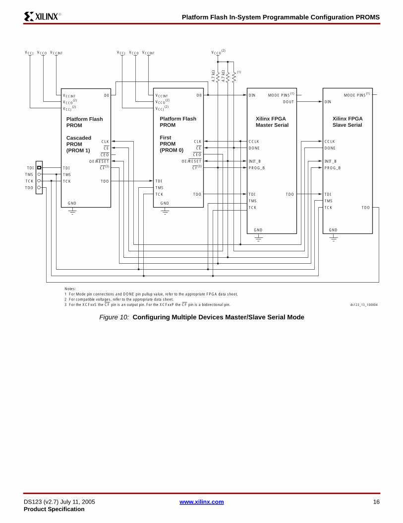
Platform Flash In-System Programmable Configuration PROMS
DS123 (v27) July 11 2005 wwwxilinxcom 16Product Specification
R
Figure 10 Configuring Multiple Devices MasterSlave Serial Mode
Platform Flash PROM
First PROM(PROM 0)
VCCINT
VCCO(2)
VCCJ(2)
TDI
TMS
TCK
D0
CLK
CE
CEO
OERESET
CF(3)
TDO
Xilinx FPGAMaster Serial
DIN
CCLK
DONE
INIT_B
PROG_B
TDI
TMS
TCK
MODE PINS(1)
DOUT
TDO
VCCJ VCCO VCCINT
47
kΩ
47
kΩ (1)
VCCO(2)
TDI
TMS
TCK
TDO
Notes1 For Mode pin connections and DONE pin pullup value refer to the appropriate FPGA data sheet2 For compatible voltages refer to the appropriate data sheet3 For the XCFxxS the CF pin is an output pin For the XCFxxP the CF pin is a bidirectional pin
Xilinx FPGASlave Serial
DIN
CCLK
DONE
INIT_B
PROG_B
TDI
TMS
TCK
Platform Flash PROM
Cascaded PROM(PROM 1)
VCCINT
VCCO(2)
VCCJ(2)
TDI
TMS
TCK
D0
CLK
CE
CEO
OERESET
CF(3)
TDO
VCCJ VCCO VCCINT
MODE PINS(1)
TDO
ds123_13_100804
GND
GNDGND
GND
Platform Flash In-System Programmable Configuration PROMS
DS123 (v27) July 11 2005 wwwxilinxcom 17Product Specification
R
Figure 11 Configuring in Master SelectMAP Mode
XCFxxPPlatform Flash PROM
VCCINT
VCCO(2)
VCCJ(2)
TDI
TMS
TCK
GND
D[07]
CLK
CE
CEO
OERESET
CF(5)
BUSY(4)
TDO
Xilinx FPGAMaster SelectMAP
D[07]
CCLK
DONE
INIT_B
PROG_B
BUSY(4)
TDI
TMS
TCK
GND
MODE PINS(1)
RDWR_B
CS_B
TDO
VCCJ VCCO VCCINT
D[07]
CCLK
DONE
INIT_B
PROG_B
BUSY(4)
47
kΩ
47
kΩ (1)
VCCO(2)
OPTIONALSlave FPGAs with identicalconfigurations
TDI
TMS
TCK
TDO
Notes1 For Mode pin connections and DONE pin pullup value refer to the appropriate FPGA data sheet2 For compatible voltages refer to the appropriate data sheet3 CS_B (or CS) and RDWR_B (or WRITE) must be either driven Low or pulled down exernally One option is shown4 The BUSY pin is only available with the XCFxxP Platform Flash PROM and the connection is only required for high-frequency SelectMAP mode configuration For BUSY pin requirements refer to the appropriate FPGA data sheet5 For the XCFxxP the CF pin is a bidirectional pin
1KΩ
1KΩ
IO(3)
IO(3)
ds123_14_100804
Platform Flash In-System Programmable Configuration PROMS
DS123 (v27) July 11 2005 wwwxilinxcom 18Product Specification
R
Figure 12 Configuring in Slave SelectMAP Mode
XCFxxPPlatform Flash PROM
VCCINT
VCCO(2)
VCCJ(2)
TDI
TMS
TCK
GND
D[07]
CLK(5)
CE
CEO
OERESET
CF(6)
BUSY(4)
TDO
Xilinx FPGASlave SelectMAP
D[07]
CCLK
DONE
INIT_B
PROG_B
BUSY(4)
TDI
TMS
TCK
GND
MODE PINS(1)
RDWR_B
CS_B
TDO
VCCJ VCCO VCCINT
D[07]
CCLK
DONE
INIT_B
PROG_B
BUSY(4)
47
kΩ
47
kΩ (1)
VCCO(2)
OPTIONALSlave FPGAs with identicalconfigurations
TDI
TMS
TCK
TDO
Notes1 For Mode pin connections and DONE pin pullup value refer to the appropriate FPGA data sheet2 For compatible voltages refer to the appropriate data sheet3 CS_B (or CS) and RDWR_B (or WRITE) must be either driven Low or pulled down exernally One option is shown4 The BUSY pin is only available with the XCFxxP Platform Flash PROM and the connection is only required for high-frequency SelectMAP mode configuration For BUSY pin requirements refer to the appropriate FPGA data sheet5 In Slave SelectMAP mode the configuration interface can be clocked by an external oscillator or optionally the CLKOUT signal can be used to drive the FPGAs configuration clock (CCLK) If the XCFxxP PROMs CLKOUT signal is used then it must be tied to a 47KΩ resistor pulled up to VCCO6 For the XCFxxP the CF pin is a bidirectional pin
1KΩ
1KΩ
IO(3)
IO(3)
ds123_15_070505
External (5)
Oscillator
Platform Flash In-System Programmable Configuration PROMS
DS123 (v27) July 11 2005 wwwxilinxcom 19Product Specification
R
Figure 13 Configuring Multiple Devices with Identical Patterns in MasterSlave SelectMAP Mode
XCFxxPPlatform Flash PROM
First PROM(PROM 0)
VCCINT
VCCO(2)
VCCJ(2)
TDI
TMS
TCK
GND
D[07]
CLK
CE
CEO
OERESET
CF(5)
BUSY(4)
TDO
Xilinx FPGAMaster SelectMAP
D[07]
CCLK
DONE
INIT_B
PROG_B
BUSY(4)
TDI
TMS
TCK
GND
MODE PINS(1)
TDO
VCCJ VCCO VCCINT
47
kΩ
47
kΩ (1)
VCCO(2)
TDI
TMS
TCK
TDO
Notes1 For Mode pin connections and DONE pin pullup value refer to the appropriate FPGA data sheet2 For compatible voltages refer to the appropriate data sheet3 CS_B (or CS) and RDWR_B (or WRITE) must be either driven Low or pulled down exernally One option is shown4 The BUSY pin is only available with the XCFxxP Platform Flash PROM and the connection is only required for high-frequency SelectMAP mode configuration For BUSY pin requirements refer to the appropriate FPGA data sheet5 For the XCFxxP the CF pin is a bidirectional pin
Xilinx FPGASlave SelectMAP
D[07]
CCLK
DONE
INIT_B
PROG_B
BUSY(4)
TDI
TMS
TCK
GND
XCFxxPPlatform Flash PROM
Cascaded PROM(PROM 1)
VCCINT
VCCO(2)
VCCJ(2)
TDI
TMS
TCK
GND
D[07]
CLK
CE
CEO
OERESET
CF(5)
BUSY(4)
TDO
VCCJ VCCO VCCINT
MODE PINS(1)
TDO
ds123_16_100804
1KΩ1K
Ω
IO(3)
IO(3)
1KΩ1K
Ω
IO(3)
IO(3)RDWR_B
CS_B
RDWR_B
CS_B
Platform Flash In-System Programmable Configuration PROMS
DS123 (v27) July 11 2005 wwwxilinxcom 20Product Specification
R
Figure 14 Configuring Multiple Devices with Design Revisioning in Slave Serial Mode
XCFxxPPlatform Flash PROM
First PROM(PROM 0)
VCCINT
VCCO(2)
VCCJ(2)
TDI
TMS
TCK
EN_EXT_SEL
REV_SEL[10]
D0
CLK(3)
CE
CEO
OERESET
CF(4)
TDO
Xilinx FPGASlave Serial
DIN
CCLK
DONE
INIT_B
PROG_B
TDI
TMS
TCK
VCCJ VCCO VCCINT
47
kΩ
47
kΩ
(1)
VCCO(2)
TDI
TMS
TCK
TDO
1 For Mode pin connections and DONE pin pullup value refer to the appropriate FPGA data sheet
2 For compatible voltages refer to the appropriate data sheet3 In Slave Serial mode the configuration interface can be clocked by an external oscillator or optionally the CLKOUT signal can be used to drive the FPGAs configuration clock (CCLK) If the XCFxxP PROMs CLKOUT signal is used then it must be tied to a 47KΩ resistor pulled up to VCCO4 For the XCFxxP the CF pin is a bidirectional pin
XCFxxPPlatform Flash PROM
Cascaded PROM(PROM 1)
VCCINT
VCCO(2)
VCCJ(2)
TDI
TMS
TCK
EN_EXT_SEL
REV_SEL[10]
D0
CLK(3)
CE
CEO
OERESET
CF(4)
TDO
VCCJ VCCO VCCINT
ds123_17_070505
Design RevisionControl Logic
EN_EXT_SEL
REV_SEL[10]
DONE
CF PROG_B
Xilinx FPGASlave Serial
DIN
CCLK
DONE
INIT_B
PROG_B
TDI
TMS
TCK
MODE PINS(1)
TDO
GNDGND
GND
DOUT
MODE PINS(1)
GND
External (3)
Oscillator
Platform Flash In-System Programmable Configuration PROMS
DS123 (v27) July 11 2005 wwwxilinxcom 21Product Specification
R
Figure 15 Configuring Multiple Devices with Design Revisioning in Slave SelectMAP Mode
XCFxxPPlatform Flash PROM
First PROM(PROM 0)
VCCINT
VCCO(2)
VCCJ(2)
TDI
TMS
TCK
EN_EXT_SEL
REV_SEL[10]
GND
D[07]
CLK(5)
CE
CEO
OERESET
CF(6)
BUSY(4)
TDO
Xilinx FPGASlave SelectMAP
D[07]
CCLK
DONE
INIT_B
PROG_B
BUSY(4)
TDI
TMS
TCK
MODE PINS(1)
RDWR_B
CS_B
TDO
VCCJ VCCO VCCINT
47
kΩ
47
kΩ
(1)
VCCO(2)
TDI
TMS
TCK
TDO
Notes
1 For Mode pin connections and DONE pin pullup value refer to the appropriate FPGA data sheet
2 For compatible voltages refer to the appropriate data sheet
3 RDWR_B (or WRITE) must be either driven Low or pulled down exernally One option is shown
4 The BUSY pin is only available with the XCFxxP Platform Flash PROM and the connection is only required for high frequency SelectMAP mode configuration For BUSY pin requirements refer to the appropriate FPGA data sheet
5 In Slave SelectMAP mode the configuration interface can be clocked by an external oscillator or optionally the CLKOUT signal can be used to drive the FPGAs configuration clock (CCLK) If the XCFxxP PROMs CLKOUT signal is used then it must be tied to a 47KΩ resistor pulled up to VCCO6 For the XCFxxP the CF pin is a bidirectional pin
Xilinx FPGASlave SelectMAP
D[07]
CCLK
DONE
INIT_B
PROG_B
BUSY(4)
TDI
TMS
TCK
MODE PINS(1)
RDWR_B
CS_B
TDO
XCFxxPPlatform Flash PROM
Cascaded PROM(PROM 1)
VCCINT
VCCO(2)
VCCJ(2)
TDI
TMS
TCK
EN_EXT_SEL
REV_SEL[10]
GND
D[07]
CLK(5)
CE
CEO
OERESET
CF(6)
BUSY(4)
TDO
VCCJ VCCO VCCINT
1KΩ
IO(3)
1KΩ
IO(3)
EN_EXT_SEL
REV_SEL[10]
CF
DONE
PROG_B
CS_B[10]
Design
Revision
Control
Logic
GND GND
ds123_18_070505
External (5)
Oscillator
Platform Flash In-System Programmable Configuration PROMS
DS123 (v27) July 11 2005 wwwxilinxcom 22Product Specification
R
Reset and Power-On Reset ActivationAt power up the device requires the VCCINT power supplyto monotonically rise to the nominal operating voltage withinthe specified VCCINT rise time If the power supply cannotmeet this requirement then the device might not performpower-on reset properly During the power-up sequenceOERESET is held Low by the PROM Once the requiredsupplies have reached their respective POR (Power OnReset) thresholds the OERESET release is delayed (TOERminimum) to allow more margin for the power supplies tostabilize before initiating configuration The OERESET pinis connected to an external 47kΩ pull-up resistor and alsoto the target FPGAs INIT pin For systems utilizing slow-ris-ing power supplies an additional power monitoring circuitcan be used to delay the target configuration until the sys-tem power reaches minimum operating voltages by holdingthe OERESET pin Low When OERESET is released theFPGArsquos INIT pin is pulled High allowing the FPGAs config-uration sequence to begin If the power drops below the
power-down threshold (VCCPD) the PROM resets andOERESET is again held Low until the after the POR thresh-old is reached OERESET polarity is not programmableThese power-up requirements are shown graphically inFigure 16For a fully powered Platform Flash PROM a reset occurswhenever OERESET is asserted (Low) or CE is deas-serted (High) The address counter is reset CEO is drivenHigh and the remaining outputs are placed in a high-imped-ance stateNotes1 The XCFxxS PROM only requires VCCINT to rise above
its POR threshold before releasing OERESET 2 The XCFxxP PROM requires both VCCINT to rise above
its POR threshold and for VCCO to reach the recommended operating voltage level before releasing OERESET
IO Input Voltage Tolerance and Power Sequencing The IOs on each re-programmable Platform Flash PROMare fully 33V-tolerant This allows 3V CMOS signals to con-nect directly to the inputs without damage The core powersupply (VCCINT) JTAG pin power supply (VCCJ) outputpower supply (VCCO) and external 3V CMOS IO signalscan be applied in any order Additionally for the XCFxxS PROM only when VCCO is sup-plied at 25V or 33V and VCCINT is supplied at 33V theIOs are 5V-tolerant This allows 5V CMOS signals to con-nect directly to the inputs on a powered XCFxxS PROMwithout damage Failure to power the PROM correctly whilesupplying a 5V input signal may result in damage to theXCFxxS device
Standby ModeThe PROM enters a low-power standby mode whenever CEis deasserted (High) In standby mode the address counteris reset CEO is driven High and the remaining outputs areplaced in a high-impedance state regardless of the state ofthe OERESET input For the device to remain in thelow-power standby mode the JTAG pins TMS TDI andTDO must not be pulled Low and TCK must be stopped(High or Low)When using the FPGA DONE signal to drive the PROM CEpin High to reduce standby power after configuration anexternal pull-up resistor should be used Typically a 330Ωpull-up resistor is used but refer to the appropriate FPGAdata sheet for the recommended DONE pin pull-up value Ifthe DONE circuit is connected to an LED to indicate FPGA
Figure 16 Platform Flash PROM Power-Up Requirements
TOER
VCCINT
VCCPOR
VCCPD
200 micros ramp50 ms ramp
TOER TRST
TIME (ms)
A slow-ramping VCCINT supply may still be below the minimum operating voltage when OERESET is released In this case the configuration sequence must be delayed until both VCCINT and VCCO have reached their recommended operating conditions
Recommended Operating Range
Delay or RestartConfiguration
ds123_21_103103
Platform Flash In-System Programmable Configuration PROMS
DS123 (v27) July 11 2005 wwwxilinxcom 23Product Specification
R
configuration is complete and is also connected to thePROM CE pin to enable low-power standby mode then anexternal buffer should be used to drive the LED circuit to
ensure valid transitions on the PROMrsquos CE pin If low-powerstandby mode is not required for the PROM then the CE pinshould be connected to ground
DC Electrical CharacteristicsThis data sheet is a Preliminary data sheet The DC characteristics are based on characterization rather than simulationFurther characteristic changes are not expected
bullAbsolute Maximum Ratings page 24bullSupply Voltage Requirements for Power-On Reset and Power-Down page 24bullRecommended Operating Conditions page 25bullQuality and Reliability Characteristics page 25bullDC Characteristics Over Operating Conditions page 26
Table 9 Truth Table for XCFxxS PROM Control InputsControl Inputs
Internal Address
Outputs
OERESET CE DATA CEO ICC
High LowIf address lt TC(2) increment Active High Active
If address = TC(2) dont change High-Z Low Reduced
Low Low Held reset High-Z High Active
X(1) High Held reset High-Z High Standby
Notes 1 X = donrsquot care2 TC = Terminal Count = highest address value TC + 1 = address 0
Table 10 Truth Table for XCFxxP PROM Control InputsControl Inputs
Internal Address
Outputs
OERESET CE CF BUSY(5) DATA CEO CLKOUT ICC
High Low High Low
If address lt TC(2) and address lt EA(3) increment Active High Active Active
If address lt TC(2) and address = EA(3) dont change High-Z High High-Z Reduced
Else If address = TC(2) dont change High-Z Low High-Z Reduced
High Low High High Unchanged Active and Unchanged High Active Active
High Low uarr X(1) Reset(4) Active High Active Active
Low Low X X Held reset(4) High-Z High High-Z Active
X High X X Held reset(4) High-Z High High-Z Standby
Notes 1 X = donrsquot care2 TC = Terminal Count = highest address value TC + 1 = address 03 For the XCFxxP with Design Revisioning enabled EA = end address (last address in the selected design revision) 4 For the XCFxxP with Design Revisioning enabled Reset = address reset to the beginning address of the selected bank If Design Revisioning is not
enabled then Reset = address reset to address 05 The BUSY input is only enabled when the XCFxxP is programmed for parallel data output and decompression is not enabled
Platform Flash In-System Programmable Configuration PROMS
DS123 (v27) July 11 2005 wwwxilinxcom 24Product Specification
R
AC Electrical CharacteristicsThis data sheet is a Preliminary data sheet The AC characteristics are based on characterization rather than simulationFurther characteristic changes are not expected
bullAC Characteristics Over Operating Conditions page 28bullAC Characteristics Over Operating Conditions When Cascading page 32
Absolute Maximum Ratings
Supply Voltage Requirements for Power-On Reset and Power-Down
Symbol DescriptionXCF01S XCF02S
XCF04SXCF08P XCF16P
XCF32P Units
VCCINT Internal supply voltage relative to GND ndash05 to +40 ndash05 to +27 V
VCCO IO supply voltage relative to GND ndash05 to +40 ndash05 to +40 V
VCCJ JTAG IO supply voltage relative to GND ndash05 to +40 ndash05 to +40 V
VIN Input voltage with respect to GNDVCCO lt 25V ndash05 to +36 ndash05 to +36 V
VCCO ge 25V ndash05 to +55 ndash05 to +36 V
VTS Voltage applied to High-Z outputVCCO lt 25V ndash05 to +36 ndash05 to +36 V
VCCO ge 25V ndash05 to +55 ndash05 to +36 V
TSTG Storage temperature (ambient) ndash65 to +150 ndash65 to +150 degC
TJ Junction temperature +125 +125 degC
Notes 1 Maximum DC undershoot below GND must be limited to either 05V or 10 mA whichever is easier to achieve During transitions the device pins can
undershoot to ndash20V or overshoot to +70V provided this over- or undershoot lasts less then 10 ns and with the forcing current being limited to 200 mA
2 Stresses beyond those listed under Absolute Maximum Ratings might cause permanent damage to the device These are stress ratings only and functional operation of the device at these or any other conditions beyond those listed under Operating Conditions is not implied Exposure to Absolute Maximum Ratings conditions for extended periods of time adversely affects device reliability
3 For soldering guidelines see the information on Packaging and Thermal Characteristics at wwwxilinxcom
Symbol Description
XCF01S XCF02S XCF04S
XCF08P XCF16P XCF32P
UnitsMin Max Min Max
TVCC VCCINT rise time from 0V to nominal voltage(2) 02 50 02 50 ms
VCCPOR POR threshold for the VCCINT supply 1 - 05 - V
TOER OERESET release delay following POR(3) 05 3 05 30 ms
VCCPD Power-down threshold for VCCINT supply - 1 - 05 V
TRSTTime required to trigger a device reset when the VCCINT supply drops below the maximum VCCPD threshold 10 - 10 - ms
Notes 1 VCCINT VCCO and VCCJ supplies may be applied in any order2 At power up the device requires the VCCINT power supply to monotonically rise to the nominal operating voltage within the specified TVCC rise time
If the power supply cannot meet this requirement then the device might not perform power-on-reset properly See Figure 16 page 223 If the VCCINT and VCCO supplies do not reach their respective recommended operating conditions before the OERESET pin is released then the
configuration data from the PROM will not be available at the recommended threshold levels The configuration sequence must be delayed until both VCCINT and VCCO have reached their recommended operating conditions
huffman
XCF08P
huffman
XCF08P
Platform Flash In-System Programmable Configuration PROMS
DS123 (v27) July 11 2005 wwwxilinxcom 25Product Specification
R
Recommended Operating Conditions
Quality and Reliability Characteristics
Symbol Description
XCF01S XCF02S XCF04S XCF08P XCF16P XCF32P
UnitsMin Typ Max Min Typ MaxVCCINT Internal voltage supply 30 33 36 165 18 20 V
VCCOSupply voltage for output drivers
33V Operation 30 33 36 30 33 36 V
25V Operation 23 25 27 23 25 27 V
18V Operation 17 18 19 17 18 19 V
15V Operation - - - TBD 15 TBD V
VCCJSupply voltage for JTAG output drivers
33V Operation 30 33 36 30 33 36 V
25V Operation 23 25 27 23 25 27 V
VILLow-level input voltage
33V Operation 0 - 08 0 - 08 V
25V Operation 0 - 08 0 - 08 V
18V Operation - - 20 VCCO - - 20 VCCO V
15V Operation - - - 0 - TBD V
VIHHigh-level input voltage
33V Operation 20 - 55 20 - 36 V
25V Operation 17 - 55 17 - 36 V
18V Operation 70 VCCO - 36 70 VCCO - 36 V
15V Operation - - - TBD - 36 V
TIN Input signal transition time(1) - - 500 - - 500 ns
VO Output voltage 0 - VCCO 0 - VCCO V
TA Operating ambient temperature ndash40 - 85 ndash40 - 85 degC
Notes 1 Input signal transition time measured between 10 VCCO and 90 VCCO
Symbol Description Min Max Units
TDR Data retention 20 - Years
NPE Programerase cycles (Endurance) 20000 - Cycles
VESD Electrostatic discharge (ESD) 2000 - Volts
huffman
XCF08P
huffman
18
Platform Flash In-System Programmable Configuration PROMS
DS123 (v27) July 11 2005 wwwxilinxcom 26Product Specification
R
DC Characteristics Over Operating Conditions
Symbol Description
XCF01S XCF02S XCF04S
XCF08P XCF16P XCF32P
UnitsTest
Conditions Min MaxTest
Conditions Min Max
VOH
High-level output voltage for 33V outputs IOH = ndash4 mA 24 - IOH = ndash4 mA 24 - V
High-level output voltage for 25V outputs IOH = ndash500 microA VCCO ndash 04
- IOH = ndash500 microA VCCO ndash 04
- V
High-level output voltage for 18V outputs IOH = ndash50 microA VCCO ndash 04
- IOH = ndash50 microA VCCO ndash 04
- V
High-level output voltage for 15V outputs - - - IOH = TBD TBD - V
VOL
Low-level output voltage for 33V outputs IOL = 4 mA - 04 IOL = 4 mA - 04 V
Low-level output voltage for 25V outputs IOL = 500 microA - 04 IOL = 500 microA - 04 V
Low-level output voltage for 18V outputs IOL = 50 microA - 04 IOL = 50 microA - 04 V
Low-level output voltage for 15V outputs - - - IOL = TBD - TBD V
ICCINT Internal voltage supply current active mode 33 MHz - 10 33 MHz - 10 mA
ICCO(1)
Output driver supply current active serial mode 33 MHz - 10 33 MHz - 10 mA
Output driver supply current active parallel mode - - - 33 MHz - 40 mA
ICCJ JTAG supply current active mode Note (2) - 5 Note (2) - 5 mA
ICCINTS Internal voltage supply current standby mode Note (3) - 5 Note (3) - 5 mA
ICCOS Output driver supply current standby mode Note (3) - 1 Note (3) - 1 mA
ICCJS JTAG supply current standby mode Note (3) - 1 Note (3) - 1 mA
IILJ JTAG pins TMS TDI and TDO pull-up current VCCJ = maxVIN = GND - 100 VCCJ = max
VIN = GND - 100 microA
IIL Input leakage current
VCCINT = maxVCCO = maxVIN = GND or
VCCO
ndash10 10
VCCINT = maxVCCO = maxVIN = GND or
VCCO
ndash10 10 microA
IIH Input and output High-Z leakage current
VCCINT = maxVCCO = maxVIN = GND or
VCCO
ndash10 10
VCCINT = maxVCCO = maxVIN = GND or
VCCO
ndash10 10 microA
IILPSource current through internal pull-ups onEN_EXT_SEL REV_SEL0 REV_SEL1
- - -
VCCINT = maxVCCO = maxVIN = GND or
VCCO
- 100 microA
IIHP Sink current through internal pull-down on BUSY - - -
VCCINT = maxVCCO = maxVIN = GND or
VCCO
-100 - microA
huffman
XCF08P
Platform Flash In-System Programmable Configuration PROMS
DS123 (v27) July 11 2005 wwwxilinxcom 27Product Specification
R
CIN Input capacitance VIN = GNDf = 10 MHz - 8 VIN = GND
f = 10 MHz - 8 pF
COUT Output capacitance VIN = GNDf = 10 MHz - 14 VIN = GND
f = 10 MHz - 14 pF
Notes 1 Output driver supply current specification based on no load conditions2 TDITMSTCK non-static (active)3 CE High OE Low and TMSTDITCK static
Symbol Description
XCF01S XCF02S XCF04S
XCF08P XCF16P XCF32P
UnitsTest
Conditions Min MaxTest
Conditions Min Max
huffman
XCF08P
Platform Flash In-System Programmable Configuration PROMS
DS123 (v27) July 11 2005 wwwxilinxcom 28Product Specification
R
AC Characteristics Over Operating Conditions
Symbol Description
XCF01S XCF02S XCF04S
XCF08P XCF16P XCF32P
UnitsMin Max Min Max
TOEOERESET to data delay(6) when VCCO = 33V or 25V - 10 - 25 ns
OERESET to data delay(6) when VCCO = 18V - 30 - 25 ns
TCECE to data delay(5) when VCCO = 33V or 25V - 15 - 25 ns
CE to data delay(5) when VCCO = 18V - 30 - 25 ns
TCACCLK to data delay(7) when VCCO = 33V or 25V - 15 - 25 ns
CLK to data delay(7) when VCCO = 18V - 30 - 25 ns
TOH
Data hold from CE OERESET or CLKwhen VCCO = 33V or 25V 0 - 5 - ns
Data hold from CE OERESET or CLKwhen VCCO = 18V 0 - 5 - ns
TDF
CE or OERESET to data float delay(2)
when VCCO = 33V or 25V - 25 - 45 ns
CE or OERESET to data float delay(2)
when VCCO = 18V - 30 - 45 ns
TCYC
Clock period(7) (serial mode) when VCCO = 33V or 25V 30 - 25 - ns
Clock period(7) (serial mode) when VCCO = 18V 67 - 25 - ns
Clock period(7) (parallel mode) when VCCO = 33V or 25V - - 30 - ns
Clock period(7) (parallel mode) when VCCO = 18V - - 30 - ns
CE
OERESET
CLK
CLKOUT(optional)
BUSY(optional)
DATA
TCE
TLC THC
TSCE
TOE TCAC
THCE
THOE
TCYC
TOH
TDFTOH
THBTSBTOEC
TCEC
TCLKO
TCOH
TCDD
CF
EN_EXT_SEL
REV_SEL[10]
TSXT THXT
TSRV THRV
ds123_22_110403
huffman
XCF08P
Platform Flash In-System Programmable Configuration PROMS
DS123 (v27) July 11 2005 wwwxilinxcom 29Product Specification
R
TLCCLK Low time(3) when VCCO = 33V or 25V 10 - 12 - ns
CLK Low time(3) when VCCO = 18V 15 - 12 - ns
THCCLK High time(3) when VCCO = 33V or 25V 10 - 12 - ns
CLK High time(3) when VCCO = 18V 15 - 12 - ns
TSCE
CE setup time to CLK (guarantees proper counting)(3)
when VCCO = 33V or 25V 20 - 30 - ns
CE setup time to CLK (guarantees proper counting)(3)
when VCCO = 18V 30 30 - ns
THCE
CE hold time (guarantees counters are reset)(5)
when VCCO = 33V or 25V 250 - 2000 - ns
CE hold time (guarantees counters are reset)(5)
when VCCO = 18V 250 - 2000 - ns
THOE
OERESET hold time (guarantees counters are reset)(6)
when VCCO = 33V or 25V 250 - 2000 - ns
OERESET hold time (guarantees counters are reset)(6)
when VCCO = 18V 250 - 2000 - ns
TSBBUSY setup time to CLK when VCCO = 33V or 25V - - 12 - ns
BUSY setup time to CLK when VCCO = 18V - - 12 - ns
THBBUSY hold time to CLK when VCCO = 33V or 25V - - 8 - ns
BUSY hold time to CLK when VCCO = 18V - - 8 - ns
TCLKO
CLK input to CLKOUT output delay when VCCO = 33V or 25V - - - 35 ns
CLK input to CLKOUT output delay when VCCO = 18V - - - 35 ns
CLK input to CLKOUT output delay when VCCO = 33V or 25V with decompression(12) - - - 35 ns
CLK input to CLKOUT output delay when VCCO = 18V with decompression(12) - - - 35 ns
TCEC
CE to CLKOUT delay(8) with CLKOUT sourced from internal oscillator when VCCO = 33V or 25V - - 0 1 micros
CE to CLKOUT delay(8) with CLKOUT sourced from internal oscillator when VCCO = 18V - - 0 1 micros
CE to CLKOUT delay(8) with CLKOUT sourced from external CLK input when VCCO = 33V or 25V - - 0 2 CLK
cycles -
CE to CLKOUT delay(8) with CLKOUT sourced from external CLK input when VCCO = 18V - - 0 2 CLK
cycles -
TOEC
OERESET to CLKOUT delay(8) with CLKOUT sourced from internal oscillator when VCCO = 33V or 25V - - 0 1 micros
OERESET to CLKOUT delay(8) with CLKOUT sourced from internal oscillator when VCCO = 18V - - 0 1 micros
OERESET to CLKOUT delay(8) with CLKOUT sourced from external CLK input when VCCO = 33V or 25V 0 2 CLK
cycles -
OERESET to CLKOUT delay(8) with CLKOUT sourced from external CLK input when VCCO = 18V 0 2 CLK
cycles -
Symbol Description
XCF01S XCF02S XCF04S
XCF08P XCF16P XCF32P
UnitsMin Max Min Max
huffman
XCF08P
Platform Flash In-System Programmable Configuration PROMS
DS123 (v27) July 11 2005 wwwxilinxcom 30Product Specification
R
TCDDCLKOUT to data delay when VCCO = 33V or 25V(9) - - - 22 ns
CLKOUT to data delay when VCCO = 18V(9) - - - 22 ns
TDDC
Data setup time to CLKOUT when VCCO = 33V or 25V with decompression(9)(12) - - 5 ns
Data setup time to CLKOUT when VCCO = 18V with decompression(9)(12) - - 5 ns
TCOH
Data hold from CLKOUT when VCCO = 33V or 25V - - 3 - ns
Data hold from CLKOUT when VCCO = 18V - - 3 - ns
Data hold from CLKOUT when VCCO = 33V or 25V with decompression(12) - - 3 - ns
Data hold from CLKOUT when VCCO = 18V with decompression(12) - - 3 - ns
TSXT
EN_EXT_SEL setup time to CF (rising edge)when VCCO = 33V or 25V - - 300 - ns
EN_EXT_SEL setup time to CF (rising edge)when VCCO = 18V - - 300 - ns
THXT
EN_EXT_SEL hold time from CF (rising edge)when VCCO = 33V or 25V - - 300 - ns
EN_EXT_SEL hold time from CF (rising edge)when VCCO = 18V - - 300 - ns
TSRV
REV_SEL setup time to CF (rising edge)when VCCO = 33V or 25V - - 300 - ns
REV_SEL setup time to CF (rising edge)when VCCO = 18V - - 300 - ns
THRV
REV_SEL hold time from CF (rising edge)when VCCO = 33V or 25V - - 300 - ns
REV_SEL hold time from CF (rising edge)when VCCO = 18V - - 300 - ns
FF
CLKOUT default (fast) frequency(10) - - 25 50 MHz
CLKOUT default (fast) frequency with decompression(12) - - 125 25 MHz
Symbol Description
XCF01S XCF02S XCF04S
XCF08P XCF16P XCF32P
UnitsMin Max Min Max
huffman
XCF08P
Platform Flash In-System Programmable Configuration PROMS
DS123 (v27) July 11 2005 wwwxilinxcom 31Product Specification
R
FS
CLKOUT alternate (slower) frequency(11) - - 125 25 MHz
CLKOUT alternate (slower) frequency with decompression(12) - - 6 125 MHz
Notes 1 AC test load = 50 pF for XCF01SXCF02SXCF04S 30 pF for XCF08PXCF16PXCF32P2 Float delays are measured with 5 pF AC loads Transition is measured at plusmn200 mV from steady-state active levels3 Guaranteed by design not tested4 All AC parameters are measured with VIL = 00V and VIH = 30V5 If THCE High lt 2 micros TCE = 2 micros6 If THOE Low lt 2 micros TOE = 2 micros7 This is the minimum possible TCYC Actual TCYC = TCAC + FPGA Data setup time
Example With the XCF32P in serial mode with VCCO at 33V if FPGA Data setup time = 15 ns then the actual TCYC = 25 ns +15 ns = 40 ns8 The delay before the enabled CLKOUT signal begins clocking data out of the device is dependent on the clocking configuration The delay before
CLKOUT is enabled will increase if decompression is enabled 9 Slower CLK frequency option may be required to meet the FPGA data sheet setup time10 Typical CLKOUT default (fast) period = 25 ns (40 MHz)11 Typical CLKOUT alternate (slower) period = 50 ns (20 MHz)12 When decompression is enabled the CLKOUT signal becomes a controlled clock output When decompressed data is available CLKOUT will toggle
at frac12 the source clock frequency (either frac12 the selected internal clock frequency or frac12 the external CLK input frequency) When decompressed data is not available the CLKOUT pin is parked High If CLKOUT is used then it must be pulled High externally using a 47kΩ pull-up to VCCO
Symbol Description
XCF01S XCF02S XCF04S
XCF08P XCF16P XCF32P
UnitsMin Max Min Max
huffman
XCF08P
huffman
XCF08P
Platform Flash In-System Programmable Configuration PROMS
DS123 (v27) July 11 2005 wwwxilinxcom 32Product Specification
R
AC Characteristics Over Operating Conditions When Cascading
Symbol Description
XCF01S XCF02S XCF04S
XCF08P XCF16P XCF32P
UnitsMin Max Min Max
TCDF
CLK to output float delay(23) when VCCO = 25V or 33V - 25 - 20 ns
CLK to output float delay(23) when VCCO = 18V - 35 - 20 ns
TOCKCLK to CEO delay(35) when VCCO = 25V or 33V - 20 - 20 ns
CLK to CEO delay(35) when VCCO = 18V - 35 - 20 ns
TOCECE to CEO delay(36) when VCCO = 25V or 33V - 20 - 80 ns
CE to CEO delay(36) when VCCO = 18V - 35 - 80 ns
TOOEOERESET to CEO delay(3) when VCCO = 25V or 33V - 20 - 80 ns
OERESET to CEO delay(3) when VCCO = 18V - 35 - 80 ns
TCOCECLKOUT to CEO delay when VCCO = 25V or 33V - - - 20 ns
CLKOUT to CEO delay when VCCO = 18V - - - 20 ns
TCODF
CLKOUT to output float delay when VCCO = 25V or 33V - - - 25 ns
CLKOUT to output float delay when VCCO = 18V - - - 25 ns
Notes 1 AC test load = 50 pF for XCF01SXCF02SXCF04S 30 pF for XCF08PXCF16PXCF32P2 Float delays are measured with 5 pF AC loads Transition is measured at plusmn200 mV from steady state active levels3 Guaranteed by design not tested4 All AC parameters are measured with VIL = 00V and VIH = 30V5 For cascaded PROMs if the FPGArsquos dual-purpose configuration data pins are set to persist as configuration pins the minimum period is increased
based on the CLK to CEO and CE to data propagation delays- TCYC minimum = TOCK + TCE + FPGA Data setup time- TCAC maximum = TOCK + TCE
6 For cascaded PROMs if the FPGArsquos dual-purpose configuration data pins become general IO pins after configuration to allow for the disable to propagate to the cascaded PROMs and to avoid contention on the data lines following configuration the minimum period is increased based on the CE to CEO and CE to data propagation delays- TCYC minimum = TOCE + TCE - TCAC maximum = TOCK + TCE
OERESET
CE
CLK
CLKOUT(optional)
DATA
CEO
TOCETOOE
First BitLast Bit
TCDFTCODF
TOCK TCOCE
ds123_23_102203
huffman
XCF08P
huffman
XCF08P
Platform Flash In-System Programmable Configuration PROMS
DS123 (v27) July 11 2005 wwwxilinxcom 33Product Specification
R
Pinouts and Pin DescriptionsThe XCFxxS Platform Flash PROM is available in the VO20 and VOG20 packages The XCFxxP Platform Flash PROM isavailable in the VO48 VOG48 FS48 and FSG48 packages This section includes
bull Table 11 XCFxxS Pin Names and Descriptions page 33bull Figure 17 VO20VOG20 Pinout Diagram (Top View) with Pin Names page 34bull Table 12 XCFxxP Pin Names and Descriptions page 35bull Figure 18 VO48VOG48 Pinout Diagram (Top View) with Pin Names page 36bull Table 13 FS48FSG48 Pin NumberName Reference page 38bull Figure 19 FS48FSG48 Pinout Diagram (Top View) page 38
Notes 1 VO20VOG20 denotes a 20-pin (TSSOP) Plastic Thin Shrink Small Outline Package 2 VO48VOG48 denotes a 48-pin (TSOP) Plastic Thin Small Outline Package3 FS48FSG48 denotes a 48-pin (TFBGA) Plastic Thin Fine Pitch Ball Grid Array (08 mm pitch)
XCFxxS Pinouts and Pin DescriptionsTable 11 provides a list of the pin names and descriptions for the XCFxxS 20-pin VO20VOG20 package
Table 11 XCFxxS Pin Names and Descriptions
Pin NameBoundary
Scan OrderBoundary
Scan Function Pin Description20-pin TSSOP (VO20VOG20)
D04 Data Out D0 is the DATA output pin to provide data for configuring an
FPGA in serial mode The D0 output is set to a high-impedance state during ISPEN (when not clamped)
13 Output Enable
CLK 0 Data InConfiguration Clock Input Each rising edge on the CLK input increments the internal address counter if the CLK input is selected CE is Low and OERESET is High
3
OERESET
20 Data In Output EnableReset (Open-Drain IO) When Low this input holds the address counter reset and the DATA output is in a high-impedance state This is a bidirectional open-drain pin that is held Low while the PROM is reset Polarity is not programmable
819 Data Out
18 Output Enable
CE 15 Data InChip Enable Input When CE is High the device is put into low-power standby mode the address counter is reset and the DATA pins are put in a high-impedance state
10
CF22 Data Out Configuration Pulse (Open-Drain Output) Allows JTAG
CONFIG instruction to initiate FPGA configuration without powering down FPGA This is an open-drain output that is pulsed Low by the JTAG CONFIG command
721 Output Enable
CEO
12 Data OutChip Enable Output Chip Enable Output (CEO) is connected to the CE input of the next PROM in the chain This output is Low when CE is Low and OERESET input is High AND the internal address counter has been incremented beyond its Terminal Count (TC) value CEO returns to High when OERESET goes Low or CE goes High
13
11 Output Enable
TMS Mode Select
JTAG Mode Select Input The state of TMS on the rising edge of TCK determines the state transitions at the Test Access Port (TAP) controller TMS has an internal 50KΩ resistive pull-up to VCCJ to provide a logic 1 to the device if the pin is not driven
5
TCK ClockJTAG Clock Input This pin is the JTAG test clock It sequences the TAP controller and all the JTAG test and programming electronics
6
Platform Flash In-System Programmable Configuration PROMS
DS123 (v27) July 11 2005 wwwxilinxcom 34Product Specification
R
XCFxxS Pinout Diagram
TDI Data In
JTAG Serial Data Input This pin is the serial input to all JTAG instruction and data registers TDI has an internal 50KΩ resistive pull-up to VCCJ to provide a logic 1 to the device if the pin is not driven
4
TDO Data Out
JTAG Serial Data Output This pin is the serial output for all JTAG instruction and data registers TDO has an internal 50KΩ resistive pull-up to VCCJ to provide a logic 1 to the system if the pin is not driven
17
VCCINT +33V Supply Positive 33V supply voltage for internal logic 18
VCCO+33V 25V or 18V IO Supply Positive 33V 25V or 18V supply voltage connected to the output voltage drivers and input buffers
19
VCCJ+33V or 25V JTAG IO Supply Positive 33V 25V or 18V supply voltage connected to the TDO output voltage driver and TCK TMS and TDI input buffers
20
GND Ground 11
DNC Do not connect (These pins must be left unconnected) 2 9 12 14 15 16
Figure 17 VO20VOG20 Pinout Diagram (Top View) with Pin Names
Table 11 XCFxxS Pin Names and Descriptions (Continued)
Pin NameBoundary
Scan OrderBoundary
Scan Function Pin Description20-pin TSSOP (VO20VOG20)
VO20VOG20Top View
ds123_02_071304
1
2
3
4
5
6
7
8
9
10
20
19
18
17
16
15
14
13
12
11
D0
(DNC)
CLK
TDI
TMS
TCK
CF
OERESET
(DNC)
CE
VCCJ
VCCO
VCCINT
TDO
(DNC)
(DNC)
CEO
(DNC)
GND
(DNC)
Platform Flash In-System Programmable Configuration PROMS
DS123 (v27) July 11 2005 wwwxilinxcom 35Product Specification
R
XCFxxP Pinouts and Pin DescriptionsTable 12 provides a list of the pin names and descriptions for the XCFxxP 48-pin VO48VOG48 and 48-pin FS48FSG48packages
Table 12 XCFxxP Pin Names and Descriptions
Pin Name
Boundary Scan Order
Boundary Scan
Function Pin Description
48-pin TSOP (VO48VOG48)
48-pin TFBGA (FS48FSG48)
D028 Data Out
D0 is the DATA output pin to provide data for configuring an FPGA in serial mode D0-D7 are the DATA output pins to provide parallel data for configuring a Xilinx FPGA in SelectMap (parallel) mode The D0 output is set to a high-impedance state during ISPEN (when not clamped)The D1-D7 outputs are set to a high-impedance state during ISPEN (when not clamped) and when serial mode is selected for configuration The D1-D7 pins can be left unconnected when the PROM is used in serial mode
28 H627 Output Enable
D126 Data Out
29 H525 Output Enable
D224 Data Out
32 E523 Output Enable
D322 Data Out
33 D521 Output Enable
D420 Data Out
43 C519 Output Enable
D518 Data Out
44 B517 Output Enable
D616 Data Out
47 A515 Output Enable
D714 Data Out
48 A613 Output Enable
CLK 01 Data In
Configuration Clock Input An internal programmable control bit selects between the internal oscillator and the CLK input pin as the clock source to control the configuration sequence Each rising edge on the CLK input increments the internal address counter if the CLK input is selected CE is Low OERESET is High BUSY is Low (parallel mode only) and CF is High
12 B3
OERESET
04 Data In Output EnableReset (Open-Drain IO)When Low this input holds the address counter reset and the DATA and CLKOUT outputs are placed in a high-impedance state This is a bidirectional open-drain pin that is held Low while the PROM is reset Polarity is not programmable
11 A303 Data Out
02 Output Enable
CE 00 Data In
Chip Enable Input When CE is High the device is put into low-power standby mode the address counter is reset and the DATA and CLKOUT outputs are placed in a high-impedance state
13 B4
CF
11 Data InConfiguration Pulse (Open-Drain IO) As an output this pin allows the JTAG CONFIG instruction to initiate FPGA configuration without powering down the FPGA This is an open-drain signal that is pulsed Low by the JTAG CONFIG command As an input on the rising edge of CF the current design revision selection is sampled and the internal address counter is reset to the start address for the selected revision If unused the CF pin should be pulled High using an external 47KΩ pull-up to VCCO
6 D110 Data Out
09 Output Enable
Platform Flash In-System Programmable Configuration PROMS
DS123 (v27) July 11 2005 wwwxilinxcom 36Product Specification
R
CEO
06 Data OutChip Enable Output Chip Enable Output (CEO) is connected to the CE input of the next PROM in the chain This output is Low when CE is Low and OERESET input is High AND the internal address counter has been incremented beyond its Terminal Count (TC) value CEO returns to High when OERESET goes Low or CE goes High
10 D2
05 Output Enable
EN_EXT_SEL 31 Data In
Enable External Selection Input When this pin is Low design revision selection is controlled by the Revision Select pins When this pin is High design revision selection is controlled by the internal programmable Revision Select control bits EN_EXT_SEL has an internal 50KΩ resistive pull-up to VCCO to provide a logic 1 to the device if the pin is not driven
25 H4
REV_SEL0 30 Data InRevision Select[10] Inputs When the EN_EXT_SEL is Low the Revision Select pins are used to select the design revision to be enabled overriding the internal programmable Revision Select control bits The Revision Select[10] inputs have an internal 50KΩ resistive pull-up to VCCO to provide a logic 1 to the device if the pins are not driven
26 G3
REV_SEL1 29 Data In 27 G4
BUSY 12 Data In
Busy Input The BUSY input is enabled when parallel mode is selected for configuration When BUSY is High the internal address counter stops incrementing and the current data remains on the data pins On the first rising edge of CLK after BUSY transitions from High to Low the data for the next address is driven on the data pins When serial mode or decompression is enabled during device programming the BUSY input is disabled BUSY has an internal 50KΩ resistive pull-down to GND to provide a logic 0 to the device if the pin is not driven
5 C1
CLKOUT
08 Data Out
Configuration Clock Output An internal Programmable control bit enables the CLKOUT signal which is sourced from either the internal oscillator or the CLK input pin Each rising edge of the selected clock source increments the internal address counter if data is available CE is Low and OERESET is High Output data is available on the rising edge of CLKOUT CLKOUT is disabled if CE is High or OERESET is Low If decompression is enabled CLKOUT is parked High when decompressed data is not ready When CLKOUT is disabled the CLKOUT pin is put into a high-Z state If CLKOUT is used then it must be pulled High externally using a 47KΩ pull-up to VCCO
9 C2
07 Output Enable
TMS Mode Select
JTAG Mode Select Input The state of TMS on the rising edge of TCK determines the state transitions at the Test Access Port (TAP) controller TMS has an internal 50KΩ resistive pull-up to VCCJ to provide a logic 1 to the device if the pin is not driven
21 E2
TCK ClockJTAG Clock Input This pin is the JTAG test clock It sequences the TAP controller and all the JTAG test and programming electronics
20 H3
TDI Data In
JTAG Serial Data Input This pin is the serial input to all JTAG instruction and data registers TDI has an internal 50KΩ resistive pull-up to VCCJ to provide a logic 1 to the device if the pin is not driven
19 G1
Table 12 XCFxxP Pin Names and Descriptions (Continued)
Pin Name
Boundary Scan Order
Boundary Scan
Function Pin Description
48-pin TSOP (VO48VOG48)
48-pin TFBGA (FS48FSG48)
Platform Flash In-System Programmable Configuration PROMS
DS123 (v27) July 11 2005 wwwxilinxcom 37Product Specification
R
XCFxxP Pinout Diagrams
Figure 18 VO48VOG48 Pinout Diagram (Top View) with Pin Names
TDO Data Out
JTAG Serial Data Output This pin is the serial output for all JTAG instruction and data registers TDO has an internal 50KΩ resistive pull-up to VCCJ to provide a logic 1 to the system if the pin is not driven
22 E6
VCCINT +18V Supply Positive 18V supply voltage for internal logic 4 15 34
B1 E1 G6
VCCO+33V 25V or 18V IO Supply Positive 33V 25V or 18V supply voltage connected to the output voltage drivers and input buffers
8 30 38 45
B2 C6 D6 G5
VCCJ+33V or 25V JTAG IO Supply Positive 33V 25V or 18V supply voltage connected to the TDO output voltage driver and TCK TMS and TDI input buffers
24 H2
GND Ground2 7
17 23 31 36
46
A1 A2 B6 F1 F5 F6
H1
DNC Do Not Connect (These pins must be left unconnected)
1 3 14 16 18 35 37 39 40 41
42
A4 C3 C4 D3 D4 E3 E4 F2 F3 F4
G2
Table 12 XCFxxP Pin Names and Descriptions (Continued)
Pin Name
Boundary Scan Order
Boundary Scan
Function Pin Description
48-pin TSOP (VO48VOG48)
48-pin TFBGA (FS48FSG48)
123456789101112131415161718192021222324
484746454443424140393837363534333231302928272625
VO48VOG48Top View
DNCGNDDNC
VCCINTBUSY
CFGND
VCCOCLKOUT
CEOOERESET
CLKCE
DNCVCCINT
DNCGNDDNCTDI
TCKTMSTDOGND
D7D6GNDVCCOD5D4DNCDNCDNCDNCVCCODNCGNDDNCVCCINTD3D2GNDVCCOD1D0REV_SEL1REV_SEL0EN_EXT_SELVCCJ
Platform Flash In-System Programmable Configuration PROMS
DS123 (v27) July 11 2005 wwwxilinxcom 38Product Specification
R
Table 13 FS48FSG48 Pin NumberName ReferencePin
Number Pin NamePin
Number Pin NameA1 GND E1 VCCINT
A2 GND E2 TMS
A3 OERESET E3 DNC
A4 DNC E4 DNC
A5 D6 E5 D2
A6 D7 E6 TDO
B1 VCCINT F1 GND
B2 VCCO F2 DNC
B3 CLK F3 DNC
B4 CE F4 DNC
B5 D5 F5 GND
B6 GND F6 GND
C1 BUSY G1 TDI
C2 CLKOUT G2 DNC
C3 DNC G3 REV_SEL0
C4 DNC G4 REV_SEL1
C5 D4 G5 VCCO
C6 VCCO G6 VCCINT
D1 CF H1 GND
D2 CEO H2 VCCJ
D3 DNC H3 TCK
D4 DNC H4 EN_EXT_SEL
D5 D3 H5 D1
D6 VCCO H6 D0
Table 13 FS48FSG48 Pin NumberName ReferencePin
Number Pin NamePin
Number Pin Name
1 2 3 4 5 6
ds121_01_071604
A
B
C
D
E
F
G
H
FS48FSG48Top View
Platform Flash In-System Programmable Configuration PROMS
DS123 (v27) July 11 2005 wwwxilinxcom 39Product Specification
R
Ordering Information
Valid Ordering Combinations
Marking Information
XCF01SVO20 C XCF08PVO48 C XCF08PFS48 C XCF01SVOG20 C XCF08PVOG48 C XCF08PFSG48 C
XCF02SVO20 C XCF16PVO48 C XCF16PFS48 C XCF02SVOG20 C XCF16PVOG48 C XCF16PFSG48 C
XCF04SVO20 C XCF32PVO48 C XCF32PFS48 C XCF04SVOG20 C XCF32PVOG48 C XCF32PFSG48 C
XCF04S VO20 C
Operating RangeProcessingC = (TA = ndash40degC to +85degC)Package Type
VO20 = 20-pin TSSOP PackageVOG20 = 20-pin TSSOP Package Pb-free
Device NumberXCF01SXCF02SXCF04S
XCF32P FS48 C
Operating RangeProcessingC = (TA = ndash40degC to +85degC)Package Type
VO48 = 48-pin TSOP PackageVOG48 = 48-pin TSOP Package Pb-freeFS48 = 48-pin TFBGA PackageFSG48 = 48-pin TFBGA Package Pb-free
Device NumberXCF08PXCF16PXCF32P
XCF04S-V
Operating RangeProcessingC = (TA = ndash40degC to +85degC)Package Type
V = 20-pin TSSOP Package (VO20)VG = 20-pin TSSOP Package Pb-free (VOG20)VO48 = 48-pin TSOP Package (VO48)VOG48 = 48-pin TSOP Package Pb-free (VOG48)F48 = 48-pin TFBGA Package (FS48)FG48 = 48-pin TFBGA Package Pb-free (FSG48)
Device NumberXCF01SXCF02SXCF04SXCF08PXCF16PXCF32P
huffman
XCF08PFS48 C
huffman
XCF08P
huffman
XCF08P
Platform Flash In-System Programmable Configuration PROMS
DS123 (v27) July 11 2005 wwwxilinxcom 40Product Specification
R
Revision HistoryThe following table shows the revision history for this document
Date Version Revision
042903 10 Xilinx Initial Release
060303 11 Made edits to all pages
110503 20 Major revision
111803 21 Pinout corrections as followsbull Table 12
- For VO48 package removed 38 from VCCINT and added it to VCCO- For FS48 package removed pin D6 from VCCINT and added it to VCCO
bull Table 13 (FS48 package) - For pin D6 changed name from VCCINT to VCCO- For pin A4 changed name from GND to DNC
bull Figure 18 (VO48 package) For pin 38 changed name from VCCINT to VCCO
121503 22 bull Added specification (47kΩ) for recommended pull-up resistor on OERESET pin to section Reset and Power-On Reset Activation page 22
bull Added paragraph to section Standby Mode page 22 concerning use of a pull-up resistor andor buffer on the DONE pin
050704 23 bull Section Features page 1 Added package styles and 33 MHz configuration speed limit to itemized features
bull Section Description page 1 and following Added state conditions for CF and BUSY to the descriptive text
bull Table 2 page 3 Updated Virtex-II configuration bitstream sizesbull Section Design Revisioning page 9 Rewrittenbull Section PROM to FPGA Configuration Mode and Connections Summary
page 10 and following five instances Added instruction to tie CF High if it is not tied to the FPGArsquos PROG_B (PROGRAM) input
bull Figure 8 page 14 through Figure 15 page 21 Added footnote indicating the directionality of the CF pin in each configuration
bull Section IO Input Voltage Tolerance and Power Sequencing page 22 Rewrittenbull Table 10 page 23 Added CF column to truth table and added an additional row to
document the Low state of CFbull Section Absolute Maximum Ratings page 24 Revised VIN and VTS for rsquoPrsquo
devices bull Section Supply Voltage Requirements for Power-On Reset and Power-Down
page 24- Revised footnote callout number on TOER from Footnote (4) to Footnote (3)- Added Footnote (2) callout to TVCC
bull Section Recommended Operating Conditions page 25 - Added Typical (Typ) parameter columns and parameters for VCCINT and
VCCOVCCJ- Added 15V operation parameter row to VIL and VIH rsquoPrsquo devices- Revised VIH Min 25V operation from 20V to 17V- Added parameter row TIN and Max parameters
bull (Continued on next page)
Platform Flash In-System Programmable Configuration PROMS
DS123 (v27) July 11 2005 wwwxilinxcom 41Product Specification
R
050704(contrsquod)
23(contrsquod)
bull Section DC Characteristics Over Operating Conditions page 26 - Added parameter row and parameters for parallel configuration mode rsquoPrsquo
devices to ICCO- Added Footnote (1) and Footnote (2) with callouts in the Test Conditions column
for ICCJ ICCINTS ICCOS and ICCJS to define active and standby mode requirements
bull Section AC Characteristics Over Operating Conditions page 28 - Corrected description for second TCAC parameter line to show parameters for
18V VCCO- Revised Footnote (7) to indicate VCCO = 33V- Applied Footnote (7) to second TCYC parameter line
bull Section AC Characteristics Over Operating Conditions When Cascading page 32 Revised Footnote (5)TCYC Min and TCAC Min formulas
bull Table 12 page 35 - Added additional state conditions to CLK description- Added function of resetting the internal address counter to CF description
072004 24 bull Added Pb-free package options VOG20 FSG48 and VOG48bull Figure 8 page 14 and Figure 9 page 15 Corrected connection name for FPGA
DOUT (OPTIONAL Daisy-chained Slave FPGAs with different configurations) from DOUT to DIN
bull Section Absolute Maximum Ratings page 24 Removed parameter TSOL from table (TSOL information can be found in Package User Guide)
bull Table 2 page 3 Removed reference to XC2VP125 FPGA
101804 25 bull Table 1 page 1 Broke out VCCO VCCJ into two separate columnsbull Table 7 page 7 Added clarification of ID code die revision bitsbull Table 8 page 8 Deleted TCKMIN2 (bypass mode) and renamed TCKMIN1 to TCKMINbull Table Recommended Operating Conditions page 25 Separated VCCO and VCCJ
parametersbull Table DC Characteristics Over Operating Conditions page 26
- Added most parameter values for XCF08P XCF16P XCF32P devices- Added Footnote (1) to ICCO specifying no-load conditions
bull Table AC Characteristics Over Operating Conditions page 28 - Added most parameter values for XCF08P XCF16P XCF32P devices- Expanded Footnote (1) to include XCF08P XCF16P XCF32P devices- Added Footnote (8) through (11) relating to CLKOUT conditions for various
parameters- Added rows to TCYC specifying parameters for parallel mode- Added rows specifying parameters with decompression for TCLKO TCOH TFF
TSF- Added TDDC (setup time with decompression)
bull Table AC Characteristics Over Operating Conditions When Cascading page 32 - Added most parameter values for XCF08P XCF16P XCF32P devices- Separated Footnote (5) into Footnotes (5) and (6) to specify different
derivations of TCYC depending on whether dual-purpose configuration pins persist as configuration pins or become general IO pins after configuration
huffman
XCF08P
huffman
XCF08P
huffman
XCF08P
huffman
XCF08P
Platform Flash In-System Programmable Configuration PROMS
DS123 (v27) July 11 2005 wwwxilinxcom 42Product Specification
R
031405 26 bull Added Virtex-4 LXFXSX configuration data to Table 2 bull Corrected Virtex-II configuration data in Table 2bull Corrected Virtex-II Pro configuration data in Table 2bull Added Spartan-3L configuration data to Table 2bull Added Spartan-3E configuration data to Table 2bull Paragraph added to FPGA Master SelectMAP (Parallel) Mode (1) page 11bull Changes to DC Characteristics
- TOER changed page 26- IOL changed for VOL page 26- VCCO added to test conditions for IIL IILP IIHPand IIH page 26 Values modified
for IILP and IIHPbull Changes to AC Characteristics
- TLC and THC modified for 18V page 29- New rows added for TCEC and TOEC page 29
bull Minor changes to grammar and punctuationbull Add explanation of Preliminary to DC and AC Electrical Characteristics
071105 27 bull Move from Preliminary to Product Specificationbull Corrections to Virtex-4 configuration bitstream valuesbull Minor changes to figures 9 14 15 and 18bull Change to Internal Oscillator description page 8bull Change to CLKOUT description page 8
- Platform Flash In-System Programmable Configuration PROMS
-
- Features
- Description
- Programming
-
- In-System Programming
-
- OERESET
-
- External Programming
- Reliability and Endurance
-
- Design Security
-
- Read Protection
- Write Protection
-
- IEEE 11491 Boundary-Scan (JTAG)
-
- Instruction Register
-
- XCFxxS Instruction Register (8 bits wide)
- XCFxxP Instruction Register (16 bits wide)
-
- Boundary Scan Register
- Identification Registers
-
- IDCODE Register
- USERCODE Register
- Customer Code Register
-
- Platform Flash PROM TAP Characteristics
-
- TAP Timing
- TAP AC Parameters
-
- Additional Features for the XCFxxP
-
- Internal Oscillator
- CLKOUT
- Decompression
- Design Revisioning
-
- PROM to FPGA Configuration Mode and Connections Summary
-
- FPGA Master Serial Mode
- FPGA Slave Serial Mode
- Serial Daisy Chain
- FPGA Master SelectMAP (Parallel) Mode
- FPGA Slave SelectMAP (Parallel) Mode
- FPGA SelectMAP (Parallel) Device Chaining
- Cascading Configuration PROMs
- Initiating FPGA Configuration
-
- Configuration PROM to FPGA Device Interface Connection Diagrams
- Reset and Power-On Reset Activation
- IO Input Voltage Tolerance and Power Sequencing
- Standby Mode
- DC Electrical Characteristics
- AC Electrical Characteristics
-
- Absolute Maximum Ratings
- Supply Voltage Requirements for Power-On Reset and Power-Down
- Recommended Operating Conditions
- Quality and Reliability Characteristics
- DC Characteristics Over Operating Conditions
- AC Characteristics Over Operating Conditions
- AC Characteristics Over Operating Conditions When Cascading
-
- Pinouts and Pin Descriptions
-
- XCFxxS Pinouts and Pin Descriptions
- XCFxxS Pinout Diagram
- XCFxxP Pinouts and Pin Descriptions
- XCFxxP Pinout Diagrams
-
- Ordering Information
- Valid Ordering Combinations
- Marking Information
- Revision History
-
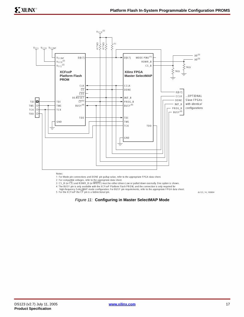
Platform Flash In-System Programmable Configuration PROMS
DS123 (v27) July 11 2005 wwwxilinxcom 17Product Specification
R
Figure 11 Configuring in Master SelectMAP Mode
XCFxxPPlatform Flash PROM
VCCINT
VCCO(2)
VCCJ(2)
TDI
TMS
TCK
GND
D[07]
CLK
CE
CEO
OERESET
CF(5)
BUSY(4)
TDO
Xilinx FPGAMaster SelectMAP
D[07]
CCLK
DONE
INIT_B
PROG_B
BUSY(4)
TDI
TMS
TCK
GND
MODE PINS(1)
RDWR_B
CS_B
TDO
VCCJ VCCO VCCINT
D[07]
CCLK
DONE
INIT_B
PROG_B
BUSY(4)
47
kΩ
47
kΩ (1)
VCCO(2)
OPTIONALSlave FPGAs with identicalconfigurations
TDI
TMS
TCK
TDO
Notes1 For Mode pin connections and DONE pin pullup value refer to the appropriate FPGA data sheet2 For compatible voltages refer to the appropriate data sheet3 CS_B (or CS) and RDWR_B (or WRITE) must be either driven Low or pulled down exernally One option is shown4 The BUSY pin is only available with the XCFxxP Platform Flash PROM and the connection is only required for high-frequency SelectMAP mode configuration For BUSY pin requirements refer to the appropriate FPGA data sheet5 For the XCFxxP the CF pin is a bidirectional pin
1KΩ
1KΩ
IO(3)
IO(3)
ds123_14_100804
Platform Flash In-System Programmable Configuration PROMS
DS123 (v27) July 11 2005 wwwxilinxcom 18Product Specification
R
Figure 12 Configuring in Slave SelectMAP Mode
XCFxxPPlatform Flash PROM
VCCINT
VCCO(2)
VCCJ(2)
TDI
TMS
TCK
GND
D[07]
CLK(5)
CE
CEO
OERESET
CF(6)
BUSY(4)
TDO
Xilinx FPGASlave SelectMAP
D[07]
CCLK
DONE
INIT_B
PROG_B
BUSY(4)
TDI
TMS
TCK
GND
MODE PINS(1)
RDWR_B
CS_B
TDO
VCCJ VCCO VCCINT
D[07]
CCLK
DONE
INIT_B
PROG_B
BUSY(4)
47
kΩ
47
kΩ (1)
VCCO(2)
OPTIONALSlave FPGAs with identicalconfigurations
TDI
TMS
TCK
TDO
Notes1 For Mode pin connections and DONE pin pullup value refer to the appropriate FPGA data sheet2 For compatible voltages refer to the appropriate data sheet3 CS_B (or CS) and RDWR_B (or WRITE) must be either driven Low or pulled down exernally One option is shown4 The BUSY pin is only available with the XCFxxP Platform Flash PROM and the connection is only required for high-frequency SelectMAP mode configuration For BUSY pin requirements refer to the appropriate FPGA data sheet5 In Slave SelectMAP mode the configuration interface can be clocked by an external oscillator or optionally the CLKOUT signal can be used to drive the FPGAs configuration clock (CCLK) If the XCFxxP PROMs CLKOUT signal is used then it must be tied to a 47KΩ resistor pulled up to VCCO6 For the XCFxxP the CF pin is a bidirectional pin
1KΩ
1KΩ
IO(3)
IO(3)
ds123_15_070505
External (5)
Oscillator
Platform Flash In-System Programmable Configuration PROMS
DS123 (v27) July 11 2005 wwwxilinxcom 19Product Specification
R
Figure 13 Configuring Multiple Devices with Identical Patterns in MasterSlave SelectMAP Mode
XCFxxPPlatform Flash PROM
First PROM(PROM 0)
VCCINT
VCCO(2)
VCCJ(2)
TDI
TMS
TCK
GND
D[07]
CLK
CE
CEO
OERESET
CF(5)
BUSY(4)
TDO
Xilinx FPGAMaster SelectMAP
D[07]
CCLK
DONE
INIT_B
PROG_B
BUSY(4)
TDI
TMS
TCK
GND
MODE PINS(1)
TDO
VCCJ VCCO VCCINT
47
kΩ
47
kΩ (1)
VCCO(2)
TDI
TMS
TCK
TDO
Notes1 For Mode pin connections and DONE pin pullup value refer to the appropriate FPGA data sheet2 For compatible voltages refer to the appropriate data sheet3 CS_B (or CS) and RDWR_B (or WRITE) must be either driven Low or pulled down exernally One option is shown4 The BUSY pin is only available with the XCFxxP Platform Flash PROM and the connection is only required for high-frequency SelectMAP mode configuration For BUSY pin requirements refer to the appropriate FPGA data sheet5 For the XCFxxP the CF pin is a bidirectional pin
Xilinx FPGASlave SelectMAP
D[07]
CCLK
DONE
INIT_B
PROG_B
BUSY(4)
TDI
TMS
TCK
GND
XCFxxPPlatform Flash PROM
Cascaded PROM(PROM 1)
VCCINT
VCCO(2)
VCCJ(2)
TDI
TMS
TCK
GND
D[07]
CLK
CE
CEO
OERESET
CF(5)
BUSY(4)
TDO
VCCJ VCCO VCCINT
MODE PINS(1)
TDO
ds123_16_100804
1KΩ1K
Ω
IO(3)
IO(3)
1KΩ1K
Ω
IO(3)
IO(3)RDWR_B
CS_B
RDWR_B
CS_B
Platform Flash In-System Programmable Configuration PROMS
DS123 (v27) July 11 2005 wwwxilinxcom 20Product Specification
R
Figure 14 Configuring Multiple Devices with Design Revisioning in Slave Serial Mode
XCFxxPPlatform Flash PROM
First PROM(PROM 0)
VCCINT
VCCO(2)
VCCJ(2)
TDI
TMS
TCK
EN_EXT_SEL
REV_SEL[10]
D0
CLK(3)
CE
CEO
OERESET
CF(4)
TDO
Xilinx FPGASlave Serial
DIN
CCLK
DONE
INIT_B
PROG_B
TDI
TMS
TCK
VCCJ VCCO VCCINT
47
kΩ
47
kΩ
(1)
VCCO(2)
TDI
TMS
TCK
TDO
1 For Mode pin connections and DONE pin pullup value refer to the appropriate FPGA data sheet
2 For compatible voltages refer to the appropriate data sheet3 In Slave Serial mode the configuration interface can be clocked by an external oscillator or optionally the CLKOUT signal can be used to drive the FPGAs configuration clock (CCLK) If the XCFxxP PROMs CLKOUT signal is used then it must be tied to a 47KΩ resistor pulled up to VCCO4 For the XCFxxP the CF pin is a bidirectional pin
XCFxxPPlatform Flash PROM
Cascaded PROM(PROM 1)
VCCINT
VCCO(2)
VCCJ(2)
TDI
TMS
TCK
EN_EXT_SEL
REV_SEL[10]
D0
CLK(3)
CE
CEO
OERESET
CF(4)
TDO
VCCJ VCCO VCCINT
ds123_17_070505
Design RevisionControl Logic
EN_EXT_SEL
REV_SEL[10]
DONE
CF PROG_B
Xilinx FPGASlave Serial
DIN
CCLK
DONE
INIT_B
PROG_B
TDI
TMS
TCK
MODE PINS(1)
TDO
GNDGND
GND
DOUT
MODE PINS(1)
GND
External (3)
Oscillator
Platform Flash In-System Programmable Configuration PROMS
DS123 (v27) July 11 2005 wwwxilinxcom 21Product Specification
R
Figure 15 Configuring Multiple Devices with Design Revisioning in Slave SelectMAP Mode
XCFxxPPlatform Flash PROM
First PROM(PROM 0)
VCCINT
VCCO(2)
VCCJ(2)
TDI
TMS
TCK
EN_EXT_SEL
REV_SEL[10]
GND
D[07]
CLK(5)
CE
CEO
OERESET
CF(6)
BUSY(4)
TDO
Xilinx FPGASlave SelectMAP
D[07]
CCLK
DONE
INIT_B
PROG_B
BUSY(4)
TDI
TMS
TCK
MODE PINS(1)
RDWR_B
CS_B
TDO
VCCJ VCCO VCCINT
47
kΩ
47
kΩ
(1)
VCCO(2)
TDI
TMS
TCK
TDO
Notes
1 For Mode pin connections and DONE pin pullup value refer to the appropriate FPGA data sheet
2 For compatible voltages refer to the appropriate data sheet
3 RDWR_B (or WRITE) must be either driven Low or pulled down exernally One option is shown
4 The BUSY pin is only available with the XCFxxP Platform Flash PROM and the connection is only required for high frequency SelectMAP mode configuration For BUSY pin requirements refer to the appropriate FPGA data sheet
5 In Slave SelectMAP mode the configuration interface can be clocked by an external oscillator or optionally the CLKOUT signal can be used to drive the FPGAs configuration clock (CCLK) If the XCFxxP PROMs CLKOUT signal is used then it must be tied to a 47KΩ resistor pulled up to VCCO6 For the XCFxxP the CF pin is a bidirectional pin
Xilinx FPGASlave SelectMAP
D[07]
CCLK
DONE
INIT_B
PROG_B
BUSY(4)
TDI
TMS
TCK
MODE PINS(1)
RDWR_B
CS_B
TDO
XCFxxPPlatform Flash PROM
Cascaded PROM(PROM 1)
VCCINT
VCCO(2)
VCCJ(2)
TDI
TMS
TCK
EN_EXT_SEL
REV_SEL[10]
GND
D[07]
CLK(5)
CE
CEO
OERESET
CF(6)
BUSY(4)
TDO
VCCJ VCCO VCCINT
1KΩ
IO(3)
1KΩ
IO(3)
EN_EXT_SEL
REV_SEL[10]
CF
DONE
PROG_B
CS_B[10]
Design
Revision
Control
Logic
GND GND
ds123_18_070505
External (5)
Oscillator
Platform Flash In-System Programmable Configuration PROMS
DS123 (v27) July 11 2005 wwwxilinxcom 22Product Specification
R
Reset and Power-On Reset ActivationAt power up the device requires the VCCINT power supplyto monotonically rise to the nominal operating voltage withinthe specified VCCINT rise time If the power supply cannotmeet this requirement then the device might not performpower-on reset properly During the power-up sequenceOERESET is held Low by the PROM Once the requiredsupplies have reached their respective POR (Power OnReset) thresholds the OERESET release is delayed (TOERminimum) to allow more margin for the power supplies tostabilize before initiating configuration The OERESET pinis connected to an external 47kΩ pull-up resistor and alsoto the target FPGAs INIT pin For systems utilizing slow-ris-ing power supplies an additional power monitoring circuitcan be used to delay the target configuration until the sys-tem power reaches minimum operating voltages by holdingthe OERESET pin Low When OERESET is released theFPGArsquos INIT pin is pulled High allowing the FPGAs config-uration sequence to begin If the power drops below the
power-down threshold (VCCPD) the PROM resets andOERESET is again held Low until the after the POR thresh-old is reached OERESET polarity is not programmableThese power-up requirements are shown graphically inFigure 16For a fully powered Platform Flash PROM a reset occurswhenever OERESET is asserted (Low) or CE is deas-serted (High) The address counter is reset CEO is drivenHigh and the remaining outputs are placed in a high-imped-ance stateNotes1 The XCFxxS PROM only requires VCCINT to rise above
its POR threshold before releasing OERESET 2 The XCFxxP PROM requires both VCCINT to rise above
its POR threshold and for VCCO to reach the recommended operating voltage level before releasing OERESET
IO Input Voltage Tolerance and Power Sequencing The IOs on each re-programmable Platform Flash PROMare fully 33V-tolerant This allows 3V CMOS signals to con-nect directly to the inputs without damage The core powersupply (VCCINT) JTAG pin power supply (VCCJ) outputpower supply (VCCO) and external 3V CMOS IO signalscan be applied in any order Additionally for the XCFxxS PROM only when VCCO is sup-plied at 25V or 33V and VCCINT is supplied at 33V theIOs are 5V-tolerant This allows 5V CMOS signals to con-nect directly to the inputs on a powered XCFxxS PROMwithout damage Failure to power the PROM correctly whilesupplying a 5V input signal may result in damage to theXCFxxS device
Standby ModeThe PROM enters a low-power standby mode whenever CEis deasserted (High) In standby mode the address counteris reset CEO is driven High and the remaining outputs areplaced in a high-impedance state regardless of the state ofthe OERESET input For the device to remain in thelow-power standby mode the JTAG pins TMS TDI andTDO must not be pulled Low and TCK must be stopped(High or Low)When using the FPGA DONE signal to drive the PROM CEpin High to reduce standby power after configuration anexternal pull-up resistor should be used Typically a 330Ωpull-up resistor is used but refer to the appropriate FPGAdata sheet for the recommended DONE pin pull-up value Ifthe DONE circuit is connected to an LED to indicate FPGA
Figure 16 Platform Flash PROM Power-Up Requirements
TOER
VCCINT
VCCPOR
VCCPD
200 micros ramp50 ms ramp
TOER TRST
TIME (ms)
A slow-ramping VCCINT supply may still be below the minimum operating voltage when OERESET is released In this case the configuration sequence must be delayed until both VCCINT and VCCO have reached their recommended operating conditions
Recommended Operating Range
Delay or RestartConfiguration
ds123_21_103103
Platform Flash In-System Programmable Configuration PROMS
DS123 (v27) July 11 2005 wwwxilinxcom 23Product Specification
R
configuration is complete and is also connected to thePROM CE pin to enable low-power standby mode then anexternal buffer should be used to drive the LED circuit to
ensure valid transitions on the PROMrsquos CE pin If low-powerstandby mode is not required for the PROM then the CE pinshould be connected to ground
DC Electrical CharacteristicsThis data sheet is a Preliminary data sheet The DC characteristics are based on characterization rather than simulationFurther characteristic changes are not expected
bullAbsolute Maximum Ratings page 24bullSupply Voltage Requirements for Power-On Reset and Power-Down page 24bullRecommended Operating Conditions page 25bullQuality and Reliability Characteristics page 25bullDC Characteristics Over Operating Conditions page 26
Table 9 Truth Table for XCFxxS PROM Control InputsControl Inputs
Internal Address
Outputs
OERESET CE DATA CEO ICC
High LowIf address lt TC(2) increment Active High Active
If address = TC(2) dont change High-Z Low Reduced
Low Low Held reset High-Z High Active
X(1) High Held reset High-Z High Standby
Notes 1 X = donrsquot care2 TC = Terminal Count = highest address value TC + 1 = address 0
Table 10 Truth Table for XCFxxP PROM Control InputsControl Inputs
Internal Address
Outputs
OERESET CE CF BUSY(5) DATA CEO CLKOUT ICC
High Low High Low
If address lt TC(2) and address lt EA(3) increment Active High Active Active
If address lt TC(2) and address = EA(3) dont change High-Z High High-Z Reduced
Else If address = TC(2) dont change High-Z Low High-Z Reduced
High Low High High Unchanged Active and Unchanged High Active Active
High Low uarr X(1) Reset(4) Active High Active Active
Low Low X X Held reset(4) High-Z High High-Z Active
X High X X Held reset(4) High-Z High High-Z Standby
Notes 1 X = donrsquot care2 TC = Terminal Count = highest address value TC + 1 = address 03 For the XCFxxP with Design Revisioning enabled EA = end address (last address in the selected design revision) 4 For the XCFxxP with Design Revisioning enabled Reset = address reset to the beginning address of the selected bank If Design Revisioning is not
enabled then Reset = address reset to address 05 The BUSY input is only enabled when the XCFxxP is programmed for parallel data output and decompression is not enabled
Platform Flash In-System Programmable Configuration PROMS
DS123 (v27) July 11 2005 wwwxilinxcom 24Product Specification
R
AC Electrical CharacteristicsThis data sheet is a Preliminary data sheet The AC characteristics are based on characterization rather than simulationFurther characteristic changes are not expected
bullAC Characteristics Over Operating Conditions page 28bullAC Characteristics Over Operating Conditions When Cascading page 32
Absolute Maximum Ratings
Supply Voltage Requirements for Power-On Reset and Power-Down
Symbol DescriptionXCF01S XCF02S
XCF04SXCF08P XCF16P
XCF32P Units
VCCINT Internal supply voltage relative to GND ndash05 to +40 ndash05 to +27 V
VCCO IO supply voltage relative to GND ndash05 to +40 ndash05 to +40 V
VCCJ JTAG IO supply voltage relative to GND ndash05 to +40 ndash05 to +40 V
VIN Input voltage with respect to GNDVCCO lt 25V ndash05 to +36 ndash05 to +36 V
VCCO ge 25V ndash05 to +55 ndash05 to +36 V
VTS Voltage applied to High-Z outputVCCO lt 25V ndash05 to +36 ndash05 to +36 V
VCCO ge 25V ndash05 to +55 ndash05 to +36 V
TSTG Storage temperature (ambient) ndash65 to +150 ndash65 to +150 degC
TJ Junction temperature +125 +125 degC
Notes 1 Maximum DC undershoot below GND must be limited to either 05V or 10 mA whichever is easier to achieve During transitions the device pins can
undershoot to ndash20V or overshoot to +70V provided this over- or undershoot lasts less then 10 ns and with the forcing current being limited to 200 mA
2 Stresses beyond those listed under Absolute Maximum Ratings might cause permanent damage to the device These are stress ratings only and functional operation of the device at these or any other conditions beyond those listed under Operating Conditions is not implied Exposure to Absolute Maximum Ratings conditions for extended periods of time adversely affects device reliability
3 For soldering guidelines see the information on Packaging and Thermal Characteristics at wwwxilinxcom
Symbol Description
XCF01S XCF02S XCF04S
XCF08P XCF16P XCF32P
UnitsMin Max Min Max
TVCC VCCINT rise time from 0V to nominal voltage(2) 02 50 02 50 ms
VCCPOR POR threshold for the VCCINT supply 1 - 05 - V
TOER OERESET release delay following POR(3) 05 3 05 30 ms
VCCPD Power-down threshold for VCCINT supply - 1 - 05 V
TRSTTime required to trigger a device reset when the VCCINT supply drops below the maximum VCCPD threshold 10 - 10 - ms
Notes 1 VCCINT VCCO and VCCJ supplies may be applied in any order2 At power up the device requires the VCCINT power supply to monotonically rise to the nominal operating voltage within the specified TVCC rise time
If the power supply cannot meet this requirement then the device might not perform power-on-reset properly See Figure 16 page 223 If the VCCINT and VCCO supplies do not reach their respective recommended operating conditions before the OERESET pin is released then the
configuration data from the PROM will not be available at the recommended threshold levels The configuration sequence must be delayed until both VCCINT and VCCO have reached their recommended operating conditions
huffman
XCF08P
huffman
XCF08P
Platform Flash In-System Programmable Configuration PROMS
DS123 (v27) July 11 2005 wwwxilinxcom 25Product Specification
R
Recommended Operating Conditions
Quality and Reliability Characteristics
Symbol Description
XCF01S XCF02S XCF04S XCF08P XCF16P XCF32P
UnitsMin Typ Max Min Typ MaxVCCINT Internal voltage supply 30 33 36 165 18 20 V
VCCOSupply voltage for output drivers
33V Operation 30 33 36 30 33 36 V
25V Operation 23 25 27 23 25 27 V
18V Operation 17 18 19 17 18 19 V
15V Operation - - - TBD 15 TBD V
VCCJSupply voltage for JTAG output drivers
33V Operation 30 33 36 30 33 36 V
25V Operation 23 25 27 23 25 27 V
VILLow-level input voltage
33V Operation 0 - 08 0 - 08 V
25V Operation 0 - 08 0 - 08 V
18V Operation - - 20 VCCO - - 20 VCCO V
15V Operation - - - 0 - TBD V
VIHHigh-level input voltage
33V Operation 20 - 55 20 - 36 V
25V Operation 17 - 55 17 - 36 V
18V Operation 70 VCCO - 36 70 VCCO - 36 V
15V Operation - - - TBD - 36 V
TIN Input signal transition time(1) - - 500 - - 500 ns
VO Output voltage 0 - VCCO 0 - VCCO V
TA Operating ambient temperature ndash40 - 85 ndash40 - 85 degC
Notes 1 Input signal transition time measured between 10 VCCO and 90 VCCO
Symbol Description Min Max Units
TDR Data retention 20 - Years
NPE Programerase cycles (Endurance) 20000 - Cycles
VESD Electrostatic discharge (ESD) 2000 - Volts
huffman
XCF08P
huffman
18
Platform Flash In-System Programmable Configuration PROMS
DS123 (v27) July 11 2005 wwwxilinxcom 26Product Specification
R
DC Characteristics Over Operating Conditions
Symbol Description
XCF01S XCF02S XCF04S
XCF08P XCF16P XCF32P
UnitsTest
Conditions Min MaxTest
Conditions Min Max
VOH
High-level output voltage for 33V outputs IOH = ndash4 mA 24 - IOH = ndash4 mA 24 - V
High-level output voltage for 25V outputs IOH = ndash500 microA VCCO ndash 04
- IOH = ndash500 microA VCCO ndash 04
- V
High-level output voltage for 18V outputs IOH = ndash50 microA VCCO ndash 04
- IOH = ndash50 microA VCCO ndash 04
- V
High-level output voltage for 15V outputs - - - IOH = TBD TBD - V
VOL
Low-level output voltage for 33V outputs IOL = 4 mA - 04 IOL = 4 mA - 04 V
Low-level output voltage for 25V outputs IOL = 500 microA - 04 IOL = 500 microA - 04 V
Low-level output voltage for 18V outputs IOL = 50 microA - 04 IOL = 50 microA - 04 V
Low-level output voltage for 15V outputs - - - IOL = TBD - TBD V
ICCINT Internal voltage supply current active mode 33 MHz - 10 33 MHz - 10 mA
ICCO(1)
Output driver supply current active serial mode 33 MHz - 10 33 MHz - 10 mA
Output driver supply current active parallel mode - - - 33 MHz - 40 mA
ICCJ JTAG supply current active mode Note (2) - 5 Note (2) - 5 mA
ICCINTS Internal voltage supply current standby mode Note (3) - 5 Note (3) - 5 mA
ICCOS Output driver supply current standby mode Note (3) - 1 Note (3) - 1 mA
ICCJS JTAG supply current standby mode Note (3) - 1 Note (3) - 1 mA
IILJ JTAG pins TMS TDI and TDO pull-up current VCCJ = maxVIN = GND - 100 VCCJ = max
VIN = GND - 100 microA
IIL Input leakage current
VCCINT = maxVCCO = maxVIN = GND or
VCCO
ndash10 10
VCCINT = maxVCCO = maxVIN = GND or
VCCO
ndash10 10 microA
IIH Input and output High-Z leakage current
VCCINT = maxVCCO = maxVIN = GND or
VCCO
ndash10 10
VCCINT = maxVCCO = maxVIN = GND or
VCCO
ndash10 10 microA
IILPSource current through internal pull-ups onEN_EXT_SEL REV_SEL0 REV_SEL1
- - -
VCCINT = maxVCCO = maxVIN = GND or
VCCO
- 100 microA
IIHP Sink current through internal pull-down on BUSY - - -
VCCINT = maxVCCO = maxVIN = GND or
VCCO
-100 - microA
huffman
XCF08P
Platform Flash In-System Programmable Configuration PROMS
DS123 (v27) July 11 2005 wwwxilinxcom 27Product Specification
R
CIN Input capacitance VIN = GNDf = 10 MHz - 8 VIN = GND
f = 10 MHz - 8 pF
COUT Output capacitance VIN = GNDf = 10 MHz - 14 VIN = GND
f = 10 MHz - 14 pF
Notes 1 Output driver supply current specification based on no load conditions2 TDITMSTCK non-static (active)3 CE High OE Low and TMSTDITCK static
Symbol Description
XCF01S XCF02S XCF04S
XCF08P XCF16P XCF32P
UnitsTest
Conditions Min MaxTest
Conditions Min Max
huffman
XCF08P
Platform Flash In-System Programmable Configuration PROMS
DS123 (v27) July 11 2005 wwwxilinxcom 28Product Specification
R
AC Characteristics Over Operating Conditions
Symbol Description
XCF01S XCF02S XCF04S
XCF08P XCF16P XCF32P
UnitsMin Max Min Max
TOEOERESET to data delay(6) when VCCO = 33V or 25V - 10 - 25 ns
OERESET to data delay(6) when VCCO = 18V - 30 - 25 ns
TCECE to data delay(5) when VCCO = 33V or 25V - 15 - 25 ns
CE to data delay(5) when VCCO = 18V - 30 - 25 ns
TCACCLK to data delay(7) when VCCO = 33V or 25V - 15 - 25 ns
CLK to data delay(7) when VCCO = 18V - 30 - 25 ns
TOH
Data hold from CE OERESET or CLKwhen VCCO = 33V or 25V 0 - 5 - ns
Data hold from CE OERESET or CLKwhen VCCO = 18V 0 - 5 - ns
TDF
CE or OERESET to data float delay(2)
when VCCO = 33V or 25V - 25 - 45 ns
CE or OERESET to data float delay(2)
when VCCO = 18V - 30 - 45 ns
TCYC
Clock period(7) (serial mode) when VCCO = 33V or 25V 30 - 25 - ns
Clock period(7) (serial mode) when VCCO = 18V 67 - 25 - ns
Clock period(7) (parallel mode) when VCCO = 33V or 25V - - 30 - ns
Clock period(7) (parallel mode) when VCCO = 18V - - 30 - ns
CE
OERESET
CLK
CLKOUT(optional)
BUSY(optional)
DATA
TCE
TLC THC
TSCE
TOE TCAC
THCE
THOE
TCYC
TOH
TDFTOH
THBTSBTOEC
TCEC
TCLKO
TCOH
TCDD
CF
EN_EXT_SEL
REV_SEL[10]
TSXT THXT
TSRV THRV
ds123_22_110403
huffman
XCF08P
Platform Flash In-System Programmable Configuration PROMS
DS123 (v27) July 11 2005 wwwxilinxcom 29Product Specification
R
TLCCLK Low time(3) when VCCO = 33V or 25V 10 - 12 - ns
CLK Low time(3) when VCCO = 18V 15 - 12 - ns
THCCLK High time(3) when VCCO = 33V or 25V 10 - 12 - ns
CLK High time(3) when VCCO = 18V 15 - 12 - ns
TSCE
CE setup time to CLK (guarantees proper counting)(3)
when VCCO = 33V or 25V 20 - 30 - ns
CE setup time to CLK (guarantees proper counting)(3)
when VCCO = 18V 30 30 - ns
THCE
CE hold time (guarantees counters are reset)(5)
when VCCO = 33V or 25V 250 - 2000 - ns
CE hold time (guarantees counters are reset)(5)
when VCCO = 18V 250 - 2000 - ns
THOE
OERESET hold time (guarantees counters are reset)(6)
when VCCO = 33V or 25V 250 - 2000 - ns
OERESET hold time (guarantees counters are reset)(6)
when VCCO = 18V 250 - 2000 - ns
TSBBUSY setup time to CLK when VCCO = 33V or 25V - - 12 - ns
BUSY setup time to CLK when VCCO = 18V - - 12 - ns
THBBUSY hold time to CLK when VCCO = 33V or 25V - - 8 - ns
BUSY hold time to CLK when VCCO = 18V - - 8 - ns
TCLKO
CLK input to CLKOUT output delay when VCCO = 33V or 25V - - - 35 ns
CLK input to CLKOUT output delay when VCCO = 18V - - - 35 ns
CLK input to CLKOUT output delay when VCCO = 33V or 25V with decompression(12) - - - 35 ns
CLK input to CLKOUT output delay when VCCO = 18V with decompression(12) - - - 35 ns
TCEC
CE to CLKOUT delay(8) with CLKOUT sourced from internal oscillator when VCCO = 33V or 25V - - 0 1 micros
CE to CLKOUT delay(8) with CLKOUT sourced from internal oscillator when VCCO = 18V - - 0 1 micros
CE to CLKOUT delay(8) with CLKOUT sourced from external CLK input when VCCO = 33V or 25V - - 0 2 CLK
cycles -
CE to CLKOUT delay(8) with CLKOUT sourced from external CLK input when VCCO = 18V - - 0 2 CLK
cycles -
TOEC
OERESET to CLKOUT delay(8) with CLKOUT sourced from internal oscillator when VCCO = 33V or 25V - - 0 1 micros
OERESET to CLKOUT delay(8) with CLKOUT sourced from internal oscillator when VCCO = 18V - - 0 1 micros
OERESET to CLKOUT delay(8) with CLKOUT sourced from external CLK input when VCCO = 33V or 25V 0 2 CLK
cycles -
OERESET to CLKOUT delay(8) with CLKOUT sourced from external CLK input when VCCO = 18V 0 2 CLK
cycles -
Symbol Description
XCF01S XCF02S XCF04S
XCF08P XCF16P XCF32P
UnitsMin Max Min Max
huffman
XCF08P
Platform Flash In-System Programmable Configuration PROMS
DS123 (v27) July 11 2005 wwwxilinxcom 30Product Specification
R
TCDDCLKOUT to data delay when VCCO = 33V or 25V(9) - - - 22 ns
CLKOUT to data delay when VCCO = 18V(9) - - - 22 ns
TDDC
Data setup time to CLKOUT when VCCO = 33V or 25V with decompression(9)(12) - - 5 ns
Data setup time to CLKOUT when VCCO = 18V with decompression(9)(12) - - 5 ns
TCOH
Data hold from CLKOUT when VCCO = 33V or 25V - - 3 - ns
Data hold from CLKOUT when VCCO = 18V - - 3 - ns
Data hold from CLKOUT when VCCO = 33V or 25V with decompression(12) - - 3 - ns
Data hold from CLKOUT when VCCO = 18V with decompression(12) - - 3 - ns
TSXT
EN_EXT_SEL setup time to CF (rising edge)when VCCO = 33V or 25V - - 300 - ns
EN_EXT_SEL setup time to CF (rising edge)when VCCO = 18V - - 300 - ns
THXT
EN_EXT_SEL hold time from CF (rising edge)when VCCO = 33V or 25V - - 300 - ns
EN_EXT_SEL hold time from CF (rising edge)when VCCO = 18V - - 300 - ns
TSRV
REV_SEL setup time to CF (rising edge)when VCCO = 33V or 25V - - 300 - ns
REV_SEL setup time to CF (rising edge)when VCCO = 18V - - 300 - ns
THRV
REV_SEL hold time from CF (rising edge)when VCCO = 33V or 25V - - 300 - ns
REV_SEL hold time from CF (rising edge)when VCCO = 18V - - 300 - ns
FF
CLKOUT default (fast) frequency(10) - - 25 50 MHz
CLKOUT default (fast) frequency with decompression(12) - - 125 25 MHz
Symbol Description
XCF01S XCF02S XCF04S
XCF08P XCF16P XCF32P
UnitsMin Max Min Max
huffman
XCF08P
Platform Flash In-System Programmable Configuration PROMS
DS123 (v27) July 11 2005 wwwxilinxcom 31Product Specification
R
FS
CLKOUT alternate (slower) frequency(11) - - 125 25 MHz
CLKOUT alternate (slower) frequency with decompression(12) - - 6 125 MHz
Notes 1 AC test load = 50 pF for XCF01SXCF02SXCF04S 30 pF for XCF08PXCF16PXCF32P2 Float delays are measured with 5 pF AC loads Transition is measured at plusmn200 mV from steady-state active levels3 Guaranteed by design not tested4 All AC parameters are measured with VIL = 00V and VIH = 30V5 If THCE High lt 2 micros TCE = 2 micros6 If THOE Low lt 2 micros TOE = 2 micros7 This is the minimum possible TCYC Actual TCYC = TCAC + FPGA Data setup time
Example With the XCF32P in serial mode with VCCO at 33V if FPGA Data setup time = 15 ns then the actual TCYC = 25 ns +15 ns = 40 ns8 The delay before the enabled CLKOUT signal begins clocking data out of the device is dependent on the clocking configuration The delay before
CLKOUT is enabled will increase if decompression is enabled 9 Slower CLK frequency option may be required to meet the FPGA data sheet setup time10 Typical CLKOUT default (fast) period = 25 ns (40 MHz)11 Typical CLKOUT alternate (slower) period = 50 ns (20 MHz)12 When decompression is enabled the CLKOUT signal becomes a controlled clock output When decompressed data is available CLKOUT will toggle
at frac12 the source clock frequency (either frac12 the selected internal clock frequency or frac12 the external CLK input frequency) When decompressed data is not available the CLKOUT pin is parked High If CLKOUT is used then it must be pulled High externally using a 47kΩ pull-up to VCCO
Symbol Description
XCF01S XCF02S XCF04S
XCF08P XCF16P XCF32P
UnitsMin Max Min Max
huffman
XCF08P
huffman
XCF08P
Platform Flash In-System Programmable Configuration PROMS
DS123 (v27) July 11 2005 wwwxilinxcom 32Product Specification
R
AC Characteristics Over Operating Conditions When Cascading
Symbol Description
XCF01S XCF02S XCF04S
XCF08P XCF16P XCF32P
UnitsMin Max Min Max
TCDF
CLK to output float delay(23) when VCCO = 25V or 33V - 25 - 20 ns
CLK to output float delay(23) when VCCO = 18V - 35 - 20 ns
TOCKCLK to CEO delay(35) when VCCO = 25V or 33V - 20 - 20 ns
CLK to CEO delay(35) when VCCO = 18V - 35 - 20 ns
TOCECE to CEO delay(36) when VCCO = 25V or 33V - 20 - 80 ns
CE to CEO delay(36) when VCCO = 18V - 35 - 80 ns
TOOEOERESET to CEO delay(3) when VCCO = 25V or 33V - 20 - 80 ns
OERESET to CEO delay(3) when VCCO = 18V - 35 - 80 ns
TCOCECLKOUT to CEO delay when VCCO = 25V or 33V - - - 20 ns
CLKOUT to CEO delay when VCCO = 18V - - - 20 ns
TCODF
CLKOUT to output float delay when VCCO = 25V or 33V - - - 25 ns
CLKOUT to output float delay when VCCO = 18V - - - 25 ns
Notes 1 AC test load = 50 pF for XCF01SXCF02SXCF04S 30 pF for XCF08PXCF16PXCF32P2 Float delays are measured with 5 pF AC loads Transition is measured at plusmn200 mV from steady state active levels3 Guaranteed by design not tested4 All AC parameters are measured with VIL = 00V and VIH = 30V5 For cascaded PROMs if the FPGArsquos dual-purpose configuration data pins are set to persist as configuration pins the minimum period is increased
based on the CLK to CEO and CE to data propagation delays- TCYC minimum = TOCK + TCE + FPGA Data setup time- TCAC maximum = TOCK + TCE
6 For cascaded PROMs if the FPGArsquos dual-purpose configuration data pins become general IO pins after configuration to allow for the disable to propagate to the cascaded PROMs and to avoid contention on the data lines following configuration the minimum period is increased based on the CE to CEO and CE to data propagation delays- TCYC minimum = TOCE + TCE - TCAC maximum = TOCK + TCE
OERESET
CE
CLK
CLKOUT(optional)
DATA
CEO
TOCETOOE
First BitLast Bit
TCDFTCODF
TOCK TCOCE
ds123_23_102203
huffman
XCF08P
huffman
XCF08P
Platform Flash In-System Programmable Configuration PROMS
DS123 (v27) July 11 2005 wwwxilinxcom 33Product Specification
R
Pinouts and Pin DescriptionsThe XCFxxS Platform Flash PROM is available in the VO20 and VOG20 packages The XCFxxP Platform Flash PROM isavailable in the VO48 VOG48 FS48 and FSG48 packages This section includes
bull Table 11 XCFxxS Pin Names and Descriptions page 33bull Figure 17 VO20VOG20 Pinout Diagram (Top View) with Pin Names page 34bull Table 12 XCFxxP Pin Names and Descriptions page 35bull Figure 18 VO48VOG48 Pinout Diagram (Top View) with Pin Names page 36bull Table 13 FS48FSG48 Pin NumberName Reference page 38bull Figure 19 FS48FSG48 Pinout Diagram (Top View) page 38
Notes 1 VO20VOG20 denotes a 20-pin (TSSOP) Plastic Thin Shrink Small Outline Package 2 VO48VOG48 denotes a 48-pin (TSOP) Plastic Thin Small Outline Package3 FS48FSG48 denotes a 48-pin (TFBGA) Plastic Thin Fine Pitch Ball Grid Array (08 mm pitch)
XCFxxS Pinouts and Pin DescriptionsTable 11 provides a list of the pin names and descriptions for the XCFxxS 20-pin VO20VOG20 package
Table 11 XCFxxS Pin Names and Descriptions
Pin NameBoundary
Scan OrderBoundary
Scan Function Pin Description20-pin TSSOP (VO20VOG20)
D04 Data Out D0 is the DATA output pin to provide data for configuring an
FPGA in serial mode The D0 output is set to a high-impedance state during ISPEN (when not clamped)
13 Output Enable
CLK 0 Data InConfiguration Clock Input Each rising edge on the CLK input increments the internal address counter if the CLK input is selected CE is Low and OERESET is High
3
OERESET
20 Data In Output EnableReset (Open-Drain IO) When Low this input holds the address counter reset and the DATA output is in a high-impedance state This is a bidirectional open-drain pin that is held Low while the PROM is reset Polarity is not programmable
819 Data Out
18 Output Enable
CE 15 Data InChip Enable Input When CE is High the device is put into low-power standby mode the address counter is reset and the DATA pins are put in a high-impedance state
10
CF22 Data Out Configuration Pulse (Open-Drain Output) Allows JTAG
CONFIG instruction to initiate FPGA configuration without powering down FPGA This is an open-drain output that is pulsed Low by the JTAG CONFIG command
721 Output Enable
CEO
12 Data OutChip Enable Output Chip Enable Output (CEO) is connected to the CE input of the next PROM in the chain This output is Low when CE is Low and OERESET input is High AND the internal address counter has been incremented beyond its Terminal Count (TC) value CEO returns to High when OERESET goes Low or CE goes High
13
11 Output Enable
TMS Mode Select
JTAG Mode Select Input The state of TMS on the rising edge of TCK determines the state transitions at the Test Access Port (TAP) controller TMS has an internal 50KΩ resistive pull-up to VCCJ to provide a logic 1 to the device if the pin is not driven
5
TCK ClockJTAG Clock Input This pin is the JTAG test clock It sequences the TAP controller and all the JTAG test and programming electronics
6
Platform Flash In-System Programmable Configuration PROMS
DS123 (v27) July 11 2005 wwwxilinxcom 34Product Specification
R
XCFxxS Pinout Diagram
TDI Data In
JTAG Serial Data Input This pin is the serial input to all JTAG instruction and data registers TDI has an internal 50KΩ resistive pull-up to VCCJ to provide a logic 1 to the device if the pin is not driven
4
TDO Data Out
JTAG Serial Data Output This pin is the serial output for all JTAG instruction and data registers TDO has an internal 50KΩ resistive pull-up to VCCJ to provide a logic 1 to the system if the pin is not driven
17
VCCINT +33V Supply Positive 33V supply voltage for internal logic 18
VCCO+33V 25V or 18V IO Supply Positive 33V 25V or 18V supply voltage connected to the output voltage drivers and input buffers
19
VCCJ+33V or 25V JTAG IO Supply Positive 33V 25V or 18V supply voltage connected to the TDO output voltage driver and TCK TMS and TDI input buffers
20
GND Ground 11
DNC Do not connect (These pins must be left unconnected) 2 9 12 14 15 16
Figure 17 VO20VOG20 Pinout Diagram (Top View) with Pin Names
Table 11 XCFxxS Pin Names and Descriptions (Continued)
Pin NameBoundary
Scan OrderBoundary
Scan Function Pin Description20-pin TSSOP (VO20VOG20)
VO20VOG20Top View
ds123_02_071304
1
2
3
4
5
6
7
8
9
10
20
19
18
17
16
15
14
13
12
11
D0
(DNC)
CLK
TDI
TMS
TCK
CF
OERESET
(DNC)
CE
VCCJ
VCCO
VCCINT
TDO
(DNC)
(DNC)
CEO
(DNC)
GND
(DNC)
Platform Flash In-System Programmable Configuration PROMS
DS123 (v27) July 11 2005 wwwxilinxcom 35Product Specification
R
XCFxxP Pinouts and Pin DescriptionsTable 12 provides a list of the pin names and descriptions for the XCFxxP 48-pin VO48VOG48 and 48-pin FS48FSG48packages
Table 12 XCFxxP Pin Names and Descriptions
Pin Name
Boundary Scan Order
Boundary Scan
Function Pin Description
48-pin TSOP (VO48VOG48)
48-pin TFBGA (FS48FSG48)
D028 Data Out
D0 is the DATA output pin to provide data for configuring an FPGA in serial mode D0-D7 are the DATA output pins to provide parallel data for configuring a Xilinx FPGA in SelectMap (parallel) mode The D0 output is set to a high-impedance state during ISPEN (when not clamped)The D1-D7 outputs are set to a high-impedance state during ISPEN (when not clamped) and when serial mode is selected for configuration The D1-D7 pins can be left unconnected when the PROM is used in serial mode
28 H627 Output Enable
D126 Data Out
29 H525 Output Enable
D224 Data Out
32 E523 Output Enable
D322 Data Out
33 D521 Output Enable
D420 Data Out
43 C519 Output Enable
D518 Data Out
44 B517 Output Enable
D616 Data Out
47 A515 Output Enable
D714 Data Out
48 A613 Output Enable
CLK 01 Data In
Configuration Clock Input An internal programmable control bit selects between the internal oscillator and the CLK input pin as the clock source to control the configuration sequence Each rising edge on the CLK input increments the internal address counter if the CLK input is selected CE is Low OERESET is High BUSY is Low (parallel mode only) and CF is High
12 B3
OERESET
04 Data In Output EnableReset (Open-Drain IO)When Low this input holds the address counter reset and the DATA and CLKOUT outputs are placed in a high-impedance state This is a bidirectional open-drain pin that is held Low while the PROM is reset Polarity is not programmable
11 A303 Data Out
02 Output Enable
CE 00 Data In
Chip Enable Input When CE is High the device is put into low-power standby mode the address counter is reset and the DATA and CLKOUT outputs are placed in a high-impedance state
13 B4
CF
11 Data InConfiguration Pulse (Open-Drain IO) As an output this pin allows the JTAG CONFIG instruction to initiate FPGA configuration without powering down the FPGA This is an open-drain signal that is pulsed Low by the JTAG CONFIG command As an input on the rising edge of CF the current design revision selection is sampled and the internal address counter is reset to the start address for the selected revision If unused the CF pin should be pulled High using an external 47KΩ pull-up to VCCO
6 D110 Data Out
09 Output Enable
Platform Flash In-System Programmable Configuration PROMS
DS123 (v27) July 11 2005 wwwxilinxcom 36Product Specification
R
CEO
06 Data OutChip Enable Output Chip Enable Output (CEO) is connected to the CE input of the next PROM in the chain This output is Low when CE is Low and OERESET input is High AND the internal address counter has been incremented beyond its Terminal Count (TC) value CEO returns to High when OERESET goes Low or CE goes High
10 D2
05 Output Enable
EN_EXT_SEL 31 Data In
Enable External Selection Input When this pin is Low design revision selection is controlled by the Revision Select pins When this pin is High design revision selection is controlled by the internal programmable Revision Select control bits EN_EXT_SEL has an internal 50KΩ resistive pull-up to VCCO to provide a logic 1 to the device if the pin is not driven
25 H4
REV_SEL0 30 Data InRevision Select[10] Inputs When the EN_EXT_SEL is Low the Revision Select pins are used to select the design revision to be enabled overriding the internal programmable Revision Select control bits The Revision Select[10] inputs have an internal 50KΩ resistive pull-up to VCCO to provide a logic 1 to the device if the pins are not driven
26 G3
REV_SEL1 29 Data In 27 G4
BUSY 12 Data In
Busy Input The BUSY input is enabled when parallel mode is selected for configuration When BUSY is High the internal address counter stops incrementing and the current data remains on the data pins On the first rising edge of CLK after BUSY transitions from High to Low the data for the next address is driven on the data pins When serial mode or decompression is enabled during device programming the BUSY input is disabled BUSY has an internal 50KΩ resistive pull-down to GND to provide a logic 0 to the device if the pin is not driven
5 C1
CLKOUT
08 Data Out
Configuration Clock Output An internal Programmable control bit enables the CLKOUT signal which is sourced from either the internal oscillator or the CLK input pin Each rising edge of the selected clock source increments the internal address counter if data is available CE is Low and OERESET is High Output data is available on the rising edge of CLKOUT CLKOUT is disabled if CE is High or OERESET is Low If decompression is enabled CLKOUT is parked High when decompressed data is not ready When CLKOUT is disabled the CLKOUT pin is put into a high-Z state If CLKOUT is used then it must be pulled High externally using a 47KΩ pull-up to VCCO
9 C2
07 Output Enable
TMS Mode Select
JTAG Mode Select Input The state of TMS on the rising edge of TCK determines the state transitions at the Test Access Port (TAP) controller TMS has an internal 50KΩ resistive pull-up to VCCJ to provide a logic 1 to the device if the pin is not driven
21 E2
TCK ClockJTAG Clock Input This pin is the JTAG test clock It sequences the TAP controller and all the JTAG test and programming electronics
20 H3
TDI Data In
JTAG Serial Data Input This pin is the serial input to all JTAG instruction and data registers TDI has an internal 50KΩ resistive pull-up to VCCJ to provide a logic 1 to the device if the pin is not driven
19 G1
Table 12 XCFxxP Pin Names and Descriptions (Continued)
Pin Name
Boundary Scan Order
Boundary Scan
Function Pin Description
48-pin TSOP (VO48VOG48)
48-pin TFBGA (FS48FSG48)
Platform Flash In-System Programmable Configuration PROMS
DS123 (v27) July 11 2005 wwwxilinxcom 37Product Specification
R
XCFxxP Pinout Diagrams
Figure 18 VO48VOG48 Pinout Diagram (Top View) with Pin Names
TDO Data Out
JTAG Serial Data Output This pin is the serial output for all JTAG instruction and data registers TDO has an internal 50KΩ resistive pull-up to VCCJ to provide a logic 1 to the system if the pin is not driven
22 E6
VCCINT +18V Supply Positive 18V supply voltage for internal logic 4 15 34
B1 E1 G6
VCCO+33V 25V or 18V IO Supply Positive 33V 25V or 18V supply voltage connected to the output voltage drivers and input buffers
8 30 38 45
B2 C6 D6 G5
VCCJ+33V or 25V JTAG IO Supply Positive 33V 25V or 18V supply voltage connected to the TDO output voltage driver and TCK TMS and TDI input buffers
24 H2
GND Ground2 7
17 23 31 36
46
A1 A2 B6 F1 F5 F6
H1
DNC Do Not Connect (These pins must be left unconnected)
1 3 14 16 18 35 37 39 40 41
42
A4 C3 C4 D3 D4 E3 E4 F2 F3 F4
G2
Table 12 XCFxxP Pin Names and Descriptions (Continued)
Pin Name
Boundary Scan Order
Boundary Scan
Function Pin Description
48-pin TSOP (VO48VOG48)
48-pin TFBGA (FS48FSG48)
123456789101112131415161718192021222324
484746454443424140393837363534333231302928272625
VO48VOG48Top View
DNCGNDDNC
VCCINTBUSY
CFGND
VCCOCLKOUT
CEOOERESET
CLKCE
DNCVCCINT
DNCGNDDNCTDI
TCKTMSTDOGND
D7D6GNDVCCOD5D4DNCDNCDNCDNCVCCODNCGNDDNCVCCINTD3D2GNDVCCOD1D0REV_SEL1REV_SEL0EN_EXT_SELVCCJ
Platform Flash In-System Programmable Configuration PROMS
DS123 (v27) July 11 2005 wwwxilinxcom 38Product Specification
R
Table 13 FS48FSG48 Pin NumberName ReferencePin
Number Pin NamePin
Number Pin NameA1 GND E1 VCCINT
A2 GND E2 TMS
A3 OERESET E3 DNC
A4 DNC E4 DNC
A5 D6 E5 D2
A6 D7 E6 TDO
B1 VCCINT F1 GND
B2 VCCO F2 DNC
B3 CLK F3 DNC
B4 CE F4 DNC
B5 D5 F5 GND
B6 GND F6 GND
C1 BUSY G1 TDI
C2 CLKOUT G2 DNC
C3 DNC G3 REV_SEL0
C4 DNC G4 REV_SEL1
C5 D4 G5 VCCO
C6 VCCO G6 VCCINT
D1 CF H1 GND
D2 CEO H2 VCCJ
D3 DNC H3 TCK
D4 DNC H4 EN_EXT_SEL
D5 D3 H5 D1
D6 VCCO H6 D0
Table 13 FS48FSG48 Pin NumberName ReferencePin
Number Pin NamePin
Number Pin Name
1 2 3 4 5 6
ds121_01_071604
A
B
C
D
E
F
G
H
FS48FSG48Top View
Platform Flash In-System Programmable Configuration PROMS
DS123 (v27) July 11 2005 wwwxilinxcom 39Product Specification
R
Ordering Information
Valid Ordering Combinations
Marking Information
XCF01SVO20 C XCF08PVO48 C XCF08PFS48 C XCF01SVOG20 C XCF08PVOG48 C XCF08PFSG48 C
XCF02SVO20 C XCF16PVO48 C XCF16PFS48 C XCF02SVOG20 C XCF16PVOG48 C XCF16PFSG48 C
XCF04SVO20 C XCF32PVO48 C XCF32PFS48 C XCF04SVOG20 C XCF32PVOG48 C XCF32PFSG48 C
XCF04S VO20 C
Operating RangeProcessingC = (TA = ndash40degC to +85degC)Package Type
VO20 = 20-pin TSSOP PackageVOG20 = 20-pin TSSOP Package Pb-free
Device NumberXCF01SXCF02SXCF04S
XCF32P FS48 C
Operating RangeProcessingC = (TA = ndash40degC to +85degC)Package Type
VO48 = 48-pin TSOP PackageVOG48 = 48-pin TSOP Package Pb-freeFS48 = 48-pin TFBGA PackageFSG48 = 48-pin TFBGA Package Pb-free
Device NumberXCF08PXCF16PXCF32P
XCF04S-V
Operating RangeProcessingC = (TA = ndash40degC to +85degC)Package Type
V = 20-pin TSSOP Package (VO20)VG = 20-pin TSSOP Package Pb-free (VOG20)VO48 = 48-pin TSOP Package (VO48)VOG48 = 48-pin TSOP Package Pb-free (VOG48)F48 = 48-pin TFBGA Package (FS48)FG48 = 48-pin TFBGA Package Pb-free (FSG48)
Device NumberXCF01SXCF02SXCF04SXCF08PXCF16PXCF32P
huffman
XCF08PFS48 C
huffman
XCF08P
huffman
XCF08P
Platform Flash In-System Programmable Configuration PROMS
DS123 (v27) July 11 2005 wwwxilinxcom 40Product Specification
R
Revision HistoryThe following table shows the revision history for this document
Date Version Revision
042903 10 Xilinx Initial Release
060303 11 Made edits to all pages
110503 20 Major revision
111803 21 Pinout corrections as followsbull Table 12
- For VO48 package removed 38 from VCCINT and added it to VCCO- For FS48 package removed pin D6 from VCCINT and added it to VCCO
bull Table 13 (FS48 package) - For pin D6 changed name from VCCINT to VCCO- For pin A4 changed name from GND to DNC
bull Figure 18 (VO48 package) For pin 38 changed name from VCCINT to VCCO
121503 22 bull Added specification (47kΩ) for recommended pull-up resistor on OERESET pin to section Reset and Power-On Reset Activation page 22
bull Added paragraph to section Standby Mode page 22 concerning use of a pull-up resistor andor buffer on the DONE pin
050704 23 bull Section Features page 1 Added package styles and 33 MHz configuration speed limit to itemized features
bull Section Description page 1 and following Added state conditions for CF and BUSY to the descriptive text
bull Table 2 page 3 Updated Virtex-II configuration bitstream sizesbull Section Design Revisioning page 9 Rewrittenbull Section PROM to FPGA Configuration Mode and Connections Summary
page 10 and following five instances Added instruction to tie CF High if it is not tied to the FPGArsquos PROG_B (PROGRAM) input
bull Figure 8 page 14 through Figure 15 page 21 Added footnote indicating the directionality of the CF pin in each configuration
bull Section IO Input Voltage Tolerance and Power Sequencing page 22 Rewrittenbull Table 10 page 23 Added CF column to truth table and added an additional row to
document the Low state of CFbull Section Absolute Maximum Ratings page 24 Revised VIN and VTS for rsquoPrsquo
devices bull Section Supply Voltage Requirements for Power-On Reset and Power-Down
page 24- Revised footnote callout number on TOER from Footnote (4) to Footnote (3)- Added Footnote (2) callout to TVCC
bull Section Recommended Operating Conditions page 25 - Added Typical (Typ) parameter columns and parameters for VCCINT and
VCCOVCCJ- Added 15V operation parameter row to VIL and VIH rsquoPrsquo devices- Revised VIH Min 25V operation from 20V to 17V- Added parameter row TIN and Max parameters
bull (Continued on next page)
Platform Flash In-System Programmable Configuration PROMS
DS123 (v27) July 11 2005 wwwxilinxcom 41Product Specification
R
050704(contrsquod)
23(contrsquod)
bull Section DC Characteristics Over Operating Conditions page 26 - Added parameter row and parameters for parallel configuration mode rsquoPrsquo
devices to ICCO- Added Footnote (1) and Footnote (2) with callouts in the Test Conditions column
for ICCJ ICCINTS ICCOS and ICCJS to define active and standby mode requirements
bull Section AC Characteristics Over Operating Conditions page 28 - Corrected description for second TCAC parameter line to show parameters for
18V VCCO- Revised Footnote (7) to indicate VCCO = 33V- Applied Footnote (7) to second TCYC parameter line
bull Section AC Characteristics Over Operating Conditions When Cascading page 32 Revised Footnote (5)TCYC Min and TCAC Min formulas
bull Table 12 page 35 - Added additional state conditions to CLK description- Added function of resetting the internal address counter to CF description
072004 24 bull Added Pb-free package options VOG20 FSG48 and VOG48bull Figure 8 page 14 and Figure 9 page 15 Corrected connection name for FPGA
DOUT (OPTIONAL Daisy-chained Slave FPGAs with different configurations) from DOUT to DIN
bull Section Absolute Maximum Ratings page 24 Removed parameter TSOL from table (TSOL information can be found in Package User Guide)
bull Table 2 page 3 Removed reference to XC2VP125 FPGA
101804 25 bull Table 1 page 1 Broke out VCCO VCCJ into two separate columnsbull Table 7 page 7 Added clarification of ID code die revision bitsbull Table 8 page 8 Deleted TCKMIN2 (bypass mode) and renamed TCKMIN1 to TCKMINbull Table Recommended Operating Conditions page 25 Separated VCCO and VCCJ
parametersbull Table DC Characteristics Over Operating Conditions page 26
- Added most parameter values for XCF08P XCF16P XCF32P devices- Added Footnote (1) to ICCO specifying no-load conditions
bull Table AC Characteristics Over Operating Conditions page 28 - Added most parameter values for XCF08P XCF16P XCF32P devices- Expanded Footnote (1) to include XCF08P XCF16P XCF32P devices- Added Footnote (8) through (11) relating to CLKOUT conditions for various
parameters- Added rows to TCYC specifying parameters for parallel mode- Added rows specifying parameters with decompression for TCLKO TCOH TFF
TSF- Added TDDC (setup time with decompression)
bull Table AC Characteristics Over Operating Conditions When Cascading page 32 - Added most parameter values for XCF08P XCF16P XCF32P devices- Separated Footnote (5) into Footnotes (5) and (6) to specify different
derivations of TCYC depending on whether dual-purpose configuration pins persist as configuration pins or become general IO pins after configuration
huffman
XCF08P
huffman
XCF08P
huffman
XCF08P
huffman
XCF08P
Platform Flash In-System Programmable Configuration PROMS
DS123 (v27) July 11 2005 wwwxilinxcom 42Product Specification
R
031405 26 bull Added Virtex-4 LXFXSX configuration data to Table 2 bull Corrected Virtex-II configuration data in Table 2bull Corrected Virtex-II Pro configuration data in Table 2bull Added Spartan-3L configuration data to Table 2bull Added Spartan-3E configuration data to Table 2bull Paragraph added to FPGA Master SelectMAP (Parallel) Mode (1) page 11bull Changes to DC Characteristics
- TOER changed page 26- IOL changed for VOL page 26- VCCO added to test conditions for IIL IILP IIHPand IIH page 26 Values modified
for IILP and IIHPbull Changes to AC Characteristics
- TLC and THC modified for 18V page 29- New rows added for TCEC and TOEC page 29
bull Minor changes to grammar and punctuationbull Add explanation of Preliminary to DC and AC Electrical Characteristics
071105 27 bull Move from Preliminary to Product Specificationbull Corrections to Virtex-4 configuration bitstream valuesbull Minor changes to figures 9 14 15 and 18bull Change to Internal Oscillator description page 8bull Change to CLKOUT description page 8
- Platform Flash In-System Programmable Configuration PROMS
-
- Features
- Description
- Programming
-
- In-System Programming
-
- OERESET
-
- External Programming
- Reliability and Endurance
-
- Design Security
-
- Read Protection
- Write Protection
-
- IEEE 11491 Boundary-Scan (JTAG)
-
- Instruction Register
-
- XCFxxS Instruction Register (8 bits wide)
- XCFxxP Instruction Register (16 bits wide)
-
- Boundary Scan Register
- Identification Registers
-
- IDCODE Register
- USERCODE Register
- Customer Code Register
-
- Platform Flash PROM TAP Characteristics
-
- TAP Timing
- TAP AC Parameters
-
- Additional Features for the XCFxxP
-
- Internal Oscillator
- CLKOUT
- Decompression
- Design Revisioning
-
- PROM to FPGA Configuration Mode and Connections Summary
-
- FPGA Master Serial Mode
- FPGA Slave Serial Mode
- Serial Daisy Chain
- FPGA Master SelectMAP (Parallel) Mode
- FPGA Slave SelectMAP (Parallel) Mode
- FPGA SelectMAP (Parallel) Device Chaining
- Cascading Configuration PROMs
- Initiating FPGA Configuration
-
- Configuration PROM to FPGA Device Interface Connection Diagrams
- Reset and Power-On Reset Activation
- IO Input Voltage Tolerance and Power Sequencing
- Standby Mode
- DC Electrical Characteristics
- AC Electrical Characteristics
-
- Absolute Maximum Ratings
- Supply Voltage Requirements for Power-On Reset and Power-Down
- Recommended Operating Conditions
- Quality and Reliability Characteristics
- DC Characteristics Over Operating Conditions
- AC Characteristics Over Operating Conditions
- AC Characteristics Over Operating Conditions When Cascading
-
- Pinouts and Pin Descriptions
-
- XCFxxS Pinouts and Pin Descriptions
- XCFxxS Pinout Diagram
- XCFxxP Pinouts and Pin Descriptions
- XCFxxP Pinout Diagrams
-
- Ordering Information
- Valid Ordering Combinations
- Marking Information
- Revision History
-
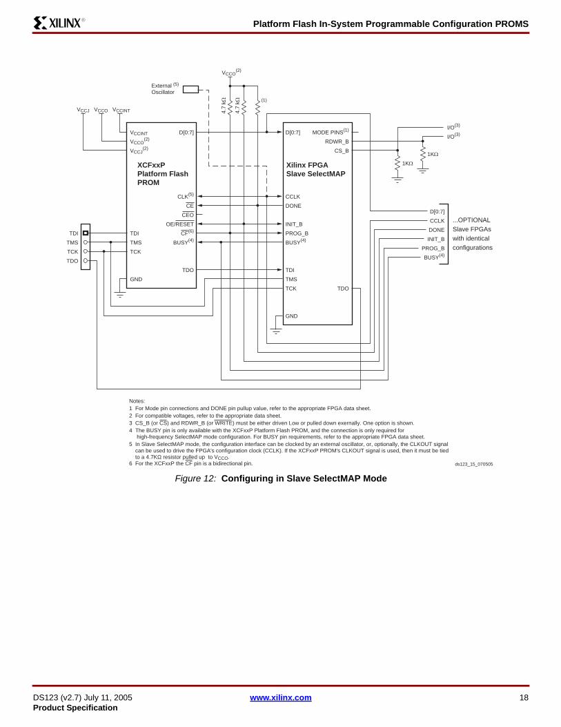
Platform Flash In-System Programmable Configuration PROMS
DS123 (v27) July 11 2005 wwwxilinxcom 19Product Specification
R
Figure 13 Configuring Multiple Devices with Identical Patterns in MasterSlave SelectMAP Mode
XCFxxPPlatform Flash PROM
First PROM(PROM 0)
VCCINT
VCCO(2)
VCCJ(2)
TDI
TMS
TCK
GND
D[07]
CLK
CE
CEO
OERESET
CF(5)
BUSY(4)
TDO
Xilinx FPGAMaster SelectMAP
D[07]
CCLK
DONE
INIT_B
PROG_B
BUSY(4)
TDI
TMS
TCK
GND
MODE PINS(1)
TDO
VCCJ VCCO VCCINT
47
kΩ
47
kΩ (1)
VCCO(2)
TDI
TMS
TCK
TDO
Notes1 For Mode pin connections and DONE pin pullup value refer to the appropriate FPGA data sheet2 For compatible voltages refer to the appropriate data sheet3 CS_B (or CS) and RDWR_B (or WRITE) must be either driven Low or pulled down exernally One option is shown4 The BUSY pin is only available with the XCFxxP Platform Flash PROM and the connection is only required for high-frequency SelectMAP mode configuration For BUSY pin requirements refer to the appropriate FPGA data sheet5 For the XCFxxP the CF pin is a bidirectional pin
Xilinx FPGASlave SelectMAP
D[07]
CCLK
DONE
INIT_B
PROG_B
BUSY(4)
TDI
TMS
TCK
GND
XCFxxPPlatform Flash PROM
Cascaded PROM(PROM 1)
VCCINT
VCCO(2)
VCCJ(2)
TDI
TMS
TCK
GND
D[07]
CLK
CE
CEO
OERESET
CF(5)
BUSY(4)
TDO
VCCJ VCCO VCCINT
MODE PINS(1)
TDO
ds123_16_100804
1KΩ1K
Ω
IO(3)
IO(3)
1KΩ1K
Ω
IO(3)
IO(3)RDWR_B
CS_B
RDWR_B
CS_B
Platform Flash In-System Programmable Configuration PROMS
DS123 (v27) July 11 2005 wwwxilinxcom 20Product Specification
R
Figure 14 Configuring Multiple Devices with Design Revisioning in Slave Serial Mode
XCFxxPPlatform Flash PROM
First PROM(PROM 0)
VCCINT
VCCO(2)
VCCJ(2)
TDI
TMS
TCK
EN_EXT_SEL
REV_SEL[10]
D0
CLK(3)
CE
CEO
OERESET
CF(4)
TDO
Xilinx FPGASlave Serial
DIN
CCLK
DONE
INIT_B
PROG_B
TDI
TMS
TCK
VCCJ VCCO VCCINT
47
kΩ
47
kΩ
(1)
VCCO(2)
TDI
TMS
TCK
TDO
1 For Mode pin connections and DONE pin pullup value refer to the appropriate FPGA data sheet
2 For compatible voltages refer to the appropriate data sheet3 In Slave Serial mode the configuration interface can be clocked by an external oscillator or optionally the CLKOUT signal can be used to drive the FPGAs configuration clock (CCLK) If the XCFxxP PROMs CLKOUT signal is used then it must be tied to a 47KΩ resistor pulled up to VCCO4 For the XCFxxP the CF pin is a bidirectional pin
XCFxxPPlatform Flash PROM
Cascaded PROM(PROM 1)
VCCINT
VCCO(2)
VCCJ(2)
TDI
TMS
TCK
EN_EXT_SEL
REV_SEL[10]
D0
CLK(3)
CE
CEO
OERESET
CF(4)
TDO
VCCJ VCCO VCCINT
ds123_17_070505
Design RevisionControl Logic
EN_EXT_SEL
REV_SEL[10]
DONE
CF PROG_B
Xilinx FPGASlave Serial
DIN
CCLK
DONE
INIT_B
PROG_B
TDI
TMS
TCK
MODE PINS(1)
TDO
GNDGND
GND
DOUT
MODE PINS(1)
GND
External (3)
Oscillator
Platform Flash In-System Programmable Configuration PROMS
DS123 (v27) July 11 2005 wwwxilinxcom 21Product Specification
R
Figure 15 Configuring Multiple Devices with Design Revisioning in Slave SelectMAP Mode
XCFxxPPlatform Flash PROM
First PROM(PROM 0)
VCCINT
VCCO(2)
VCCJ(2)
TDI
TMS
TCK
EN_EXT_SEL
REV_SEL[10]
GND
D[07]
CLK(5)
CE
CEO
OERESET
CF(6)
BUSY(4)
TDO
Xilinx FPGASlave SelectMAP
D[07]
CCLK
DONE
INIT_B
PROG_B
BUSY(4)
TDI
TMS
TCK
MODE PINS(1)
RDWR_B
CS_B
TDO
VCCJ VCCO VCCINT
47
kΩ
47
kΩ
(1)
VCCO(2)
TDI
TMS
TCK
TDO
Notes
1 For Mode pin connections and DONE pin pullup value refer to the appropriate FPGA data sheet
2 For compatible voltages refer to the appropriate data sheet
3 RDWR_B (or WRITE) must be either driven Low or pulled down exernally One option is shown
4 The BUSY pin is only available with the XCFxxP Platform Flash PROM and the connection is only required for high frequency SelectMAP mode configuration For BUSY pin requirements refer to the appropriate FPGA data sheet
5 In Slave SelectMAP mode the configuration interface can be clocked by an external oscillator or optionally the CLKOUT signal can be used to drive the FPGAs configuration clock (CCLK) If the XCFxxP PROMs CLKOUT signal is used then it must be tied to a 47KΩ resistor pulled up to VCCO6 For the XCFxxP the CF pin is a bidirectional pin
Xilinx FPGASlave SelectMAP
D[07]
CCLK
DONE
INIT_B
PROG_B
BUSY(4)
TDI
TMS
TCK
MODE PINS(1)
RDWR_B
CS_B
TDO
XCFxxPPlatform Flash PROM
Cascaded PROM(PROM 1)
VCCINT
VCCO(2)
VCCJ(2)
TDI
TMS
TCK
EN_EXT_SEL
REV_SEL[10]
GND
D[07]
CLK(5)
CE
CEO
OERESET
CF(6)
BUSY(4)
TDO
VCCJ VCCO VCCINT
1KΩ
IO(3)
1KΩ
IO(3)
EN_EXT_SEL
REV_SEL[10]
CF
DONE
PROG_B
CS_B[10]
Design
Revision
Control
Logic
GND GND
ds123_18_070505
External (5)
Oscillator
Platform Flash In-System Programmable Configuration PROMS
DS123 (v27) July 11 2005 wwwxilinxcom 22Product Specification
R
Reset and Power-On Reset ActivationAt power up the device requires the VCCINT power supplyto monotonically rise to the nominal operating voltage withinthe specified VCCINT rise time If the power supply cannotmeet this requirement then the device might not performpower-on reset properly During the power-up sequenceOERESET is held Low by the PROM Once the requiredsupplies have reached their respective POR (Power OnReset) thresholds the OERESET release is delayed (TOERminimum) to allow more margin for the power supplies tostabilize before initiating configuration The OERESET pinis connected to an external 47kΩ pull-up resistor and alsoto the target FPGAs INIT pin For systems utilizing slow-ris-ing power supplies an additional power monitoring circuitcan be used to delay the target configuration until the sys-tem power reaches minimum operating voltages by holdingthe OERESET pin Low When OERESET is released theFPGArsquos INIT pin is pulled High allowing the FPGAs config-uration sequence to begin If the power drops below the
power-down threshold (VCCPD) the PROM resets andOERESET is again held Low until the after the POR thresh-old is reached OERESET polarity is not programmableThese power-up requirements are shown graphically inFigure 16For a fully powered Platform Flash PROM a reset occurswhenever OERESET is asserted (Low) or CE is deas-serted (High) The address counter is reset CEO is drivenHigh and the remaining outputs are placed in a high-imped-ance stateNotes1 The XCFxxS PROM only requires VCCINT to rise above
its POR threshold before releasing OERESET 2 The XCFxxP PROM requires both VCCINT to rise above
its POR threshold and for VCCO to reach the recommended operating voltage level before releasing OERESET
IO Input Voltage Tolerance and Power Sequencing The IOs on each re-programmable Platform Flash PROMare fully 33V-tolerant This allows 3V CMOS signals to con-nect directly to the inputs without damage The core powersupply (VCCINT) JTAG pin power supply (VCCJ) outputpower supply (VCCO) and external 3V CMOS IO signalscan be applied in any order Additionally for the XCFxxS PROM only when VCCO is sup-plied at 25V or 33V and VCCINT is supplied at 33V theIOs are 5V-tolerant This allows 5V CMOS signals to con-nect directly to the inputs on a powered XCFxxS PROMwithout damage Failure to power the PROM correctly whilesupplying a 5V input signal may result in damage to theXCFxxS device
Standby ModeThe PROM enters a low-power standby mode whenever CEis deasserted (High) In standby mode the address counteris reset CEO is driven High and the remaining outputs areplaced in a high-impedance state regardless of the state ofthe OERESET input For the device to remain in thelow-power standby mode the JTAG pins TMS TDI andTDO must not be pulled Low and TCK must be stopped(High or Low)When using the FPGA DONE signal to drive the PROM CEpin High to reduce standby power after configuration anexternal pull-up resistor should be used Typically a 330Ωpull-up resistor is used but refer to the appropriate FPGAdata sheet for the recommended DONE pin pull-up value Ifthe DONE circuit is connected to an LED to indicate FPGA
Figure 16 Platform Flash PROM Power-Up Requirements
TOER
VCCINT
VCCPOR
VCCPD
200 micros ramp50 ms ramp
TOER TRST
TIME (ms)
A slow-ramping VCCINT supply may still be below the minimum operating voltage when OERESET is released In this case the configuration sequence must be delayed until both VCCINT and VCCO have reached their recommended operating conditions
Recommended Operating Range
Delay or RestartConfiguration
ds123_21_103103
Platform Flash In-System Programmable Configuration PROMS
DS123 (v27) July 11 2005 wwwxilinxcom 23Product Specification
R
configuration is complete and is also connected to thePROM CE pin to enable low-power standby mode then anexternal buffer should be used to drive the LED circuit to
ensure valid transitions on the PROMrsquos CE pin If low-powerstandby mode is not required for the PROM then the CE pinshould be connected to ground
DC Electrical CharacteristicsThis data sheet is a Preliminary data sheet The DC characteristics are based on characterization rather than simulationFurther characteristic changes are not expected
bullAbsolute Maximum Ratings page 24bullSupply Voltage Requirements for Power-On Reset and Power-Down page 24bullRecommended Operating Conditions page 25bullQuality and Reliability Characteristics page 25bullDC Characteristics Over Operating Conditions page 26
Table 9 Truth Table for XCFxxS PROM Control InputsControl Inputs
Internal Address
Outputs
OERESET CE DATA CEO ICC
High LowIf address lt TC(2) increment Active High Active
If address = TC(2) dont change High-Z Low Reduced
Low Low Held reset High-Z High Active
X(1) High Held reset High-Z High Standby
Notes 1 X = donrsquot care2 TC = Terminal Count = highest address value TC + 1 = address 0
Table 10 Truth Table for XCFxxP PROM Control InputsControl Inputs
Internal Address
Outputs
OERESET CE CF BUSY(5) DATA CEO CLKOUT ICC
High Low High Low
If address lt TC(2) and address lt EA(3) increment Active High Active Active
If address lt TC(2) and address = EA(3) dont change High-Z High High-Z Reduced
Else If address = TC(2) dont change High-Z Low High-Z Reduced
High Low High High Unchanged Active and Unchanged High Active Active
High Low uarr X(1) Reset(4) Active High Active Active
Low Low X X Held reset(4) High-Z High High-Z Active
X High X X Held reset(4) High-Z High High-Z Standby
Notes 1 X = donrsquot care2 TC = Terminal Count = highest address value TC + 1 = address 03 For the XCFxxP with Design Revisioning enabled EA = end address (last address in the selected design revision) 4 For the XCFxxP with Design Revisioning enabled Reset = address reset to the beginning address of the selected bank If Design Revisioning is not
enabled then Reset = address reset to address 05 The BUSY input is only enabled when the XCFxxP is programmed for parallel data output and decompression is not enabled
Platform Flash In-System Programmable Configuration PROMS
DS123 (v27) July 11 2005 wwwxilinxcom 24Product Specification
R
AC Electrical CharacteristicsThis data sheet is a Preliminary data sheet The AC characteristics are based on characterization rather than simulationFurther characteristic changes are not expected
bullAC Characteristics Over Operating Conditions page 28bullAC Characteristics Over Operating Conditions When Cascading page 32
Absolute Maximum Ratings
Supply Voltage Requirements for Power-On Reset and Power-Down
Symbol DescriptionXCF01S XCF02S
XCF04SXCF08P XCF16P
XCF32P Units
VCCINT Internal supply voltage relative to GND ndash05 to +40 ndash05 to +27 V
VCCO IO supply voltage relative to GND ndash05 to +40 ndash05 to +40 V
VCCJ JTAG IO supply voltage relative to GND ndash05 to +40 ndash05 to +40 V
VIN Input voltage with respect to GNDVCCO lt 25V ndash05 to +36 ndash05 to +36 V
VCCO ge 25V ndash05 to +55 ndash05 to +36 V
VTS Voltage applied to High-Z outputVCCO lt 25V ndash05 to +36 ndash05 to +36 V
VCCO ge 25V ndash05 to +55 ndash05 to +36 V
TSTG Storage temperature (ambient) ndash65 to +150 ndash65 to +150 degC
TJ Junction temperature +125 +125 degC
Notes 1 Maximum DC undershoot below GND must be limited to either 05V or 10 mA whichever is easier to achieve During transitions the device pins can
undershoot to ndash20V or overshoot to +70V provided this over- or undershoot lasts less then 10 ns and with the forcing current being limited to 200 mA
2 Stresses beyond those listed under Absolute Maximum Ratings might cause permanent damage to the device These are stress ratings only and functional operation of the device at these or any other conditions beyond those listed under Operating Conditions is not implied Exposure to Absolute Maximum Ratings conditions for extended periods of time adversely affects device reliability
3 For soldering guidelines see the information on Packaging and Thermal Characteristics at wwwxilinxcom
Symbol Description
XCF01S XCF02S XCF04S
XCF08P XCF16P XCF32P
UnitsMin Max Min Max
TVCC VCCINT rise time from 0V to nominal voltage(2) 02 50 02 50 ms
VCCPOR POR threshold for the VCCINT supply 1 - 05 - V
TOER OERESET release delay following POR(3) 05 3 05 30 ms
VCCPD Power-down threshold for VCCINT supply - 1 - 05 V
TRSTTime required to trigger a device reset when the VCCINT supply drops below the maximum VCCPD threshold 10 - 10 - ms
Notes 1 VCCINT VCCO and VCCJ supplies may be applied in any order2 At power up the device requires the VCCINT power supply to monotonically rise to the nominal operating voltage within the specified TVCC rise time
If the power supply cannot meet this requirement then the device might not perform power-on-reset properly See Figure 16 page 223 If the VCCINT and VCCO supplies do not reach their respective recommended operating conditions before the OERESET pin is released then the
configuration data from the PROM will not be available at the recommended threshold levels The configuration sequence must be delayed until both VCCINT and VCCO have reached their recommended operating conditions
huffman
XCF08P
huffman
XCF08P
Platform Flash In-System Programmable Configuration PROMS
DS123 (v27) July 11 2005 wwwxilinxcom 25Product Specification
R
Recommended Operating Conditions
Quality and Reliability Characteristics
Symbol Description
XCF01S XCF02S XCF04S XCF08P XCF16P XCF32P
UnitsMin Typ Max Min Typ MaxVCCINT Internal voltage supply 30 33 36 165 18 20 V
VCCOSupply voltage for output drivers
33V Operation 30 33 36 30 33 36 V
25V Operation 23 25 27 23 25 27 V
18V Operation 17 18 19 17 18 19 V
15V Operation - - - TBD 15 TBD V
VCCJSupply voltage for JTAG output drivers
33V Operation 30 33 36 30 33 36 V
25V Operation 23 25 27 23 25 27 V
VILLow-level input voltage
33V Operation 0 - 08 0 - 08 V
25V Operation 0 - 08 0 - 08 V
18V Operation - - 20 VCCO - - 20 VCCO V
15V Operation - - - 0 - TBD V
VIHHigh-level input voltage
33V Operation 20 - 55 20 - 36 V
25V Operation 17 - 55 17 - 36 V
18V Operation 70 VCCO - 36 70 VCCO - 36 V
15V Operation - - - TBD - 36 V
TIN Input signal transition time(1) - - 500 - - 500 ns
VO Output voltage 0 - VCCO 0 - VCCO V
TA Operating ambient temperature ndash40 - 85 ndash40 - 85 degC
Notes 1 Input signal transition time measured between 10 VCCO and 90 VCCO
Symbol Description Min Max Units
TDR Data retention 20 - Years
NPE Programerase cycles (Endurance) 20000 - Cycles
VESD Electrostatic discharge (ESD) 2000 - Volts
huffman
XCF08P
huffman
18
Platform Flash In-System Programmable Configuration PROMS
DS123 (v27) July 11 2005 wwwxilinxcom 26Product Specification
R
DC Characteristics Over Operating Conditions
Symbol Description
XCF01S XCF02S XCF04S
XCF08P XCF16P XCF32P
UnitsTest
Conditions Min MaxTest
Conditions Min Max
VOH
High-level output voltage for 33V outputs IOH = ndash4 mA 24 - IOH = ndash4 mA 24 - V
High-level output voltage for 25V outputs IOH = ndash500 microA VCCO ndash 04
- IOH = ndash500 microA VCCO ndash 04
- V
High-level output voltage for 18V outputs IOH = ndash50 microA VCCO ndash 04
- IOH = ndash50 microA VCCO ndash 04
- V
High-level output voltage for 15V outputs - - - IOH = TBD TBD - V
VOL
Low-level output voltage for 33V outputs IOL = 4 mA - 04 IOL = 4 mA - 04 V
Low-level output voltage for 25V outputs IOL = 500 microA - 04 IOL = 500 microA - 04 V
Low-level output voltage for 18V outputs IOL = 50 microA - 04 IOL = 50 microA - 04 V
Low-level output voltage for 15V outputs - - - IOL = TBD - TBD V
ICCINT Internal voltage supply current active mode 33 MHz - 10 33 MHz - 10 mA
ICCO(1)
Output driver supply current active serial mode 33 MHz - 10 33 MHz - 10 mA
Output driver supply current active parallel mode - - - 33 MHz - 40 mA
ICCJ JTAG supply current active mode Note (2) - 5 Note (2) - 5 mA
ICCINTS Internal voltage supply current standby mode Note (3) - 5 Note (3) - 5 mA
ICCOS Output driver supply current standby mode Note (3) - 1 Note (3) - 1 mA
ICCJS JTAG supply current standby mode Note (3) - 1 Note (3) - 1 mA
IILJ JTAG pins TMS TDI and TDO pull-up current VCCJ = maxVIN = GND - 100 VCCJ = max
VIN = GND - 100 microA
IIL Input leakage current
VCCINT = maxVCCO = maxVIN = GND or
VCCO
ndash10 10
VCCINT = maxVCCO = maxVIN = GND or
VCCO
ndash10 10 microA
IIH Input and output High-Z leakage current
VCCINT = maxVCCO = maxVIN = GND or
VCCO
ndash10 10
VCCINT = maxVCCO = maxVIN = GND or
VCCO
ndash10 10 microA
IILPSource current through internal pull-ups onEN_EXT_SEL REV_SEL0 REV_SEL1
- - -
VCCINT = maxVCCO = maxVIN = GND or
VCCO
- 100 microA
IIHP Sink current through internal pull-down on BUSY - - -
VCCINT = maxVCCO = maxVIN = GND or
VCCO
-100 - microA
huffman
XCF08P
Platform Flash In-System Programmable Configuration PROMS
DS123 (v27) July 11 2005 wwwxilinxcom 27Product Specification
R
CIN Input capacitance VIN = GNDf = 10 MHz - 8 VIN = GND
f = 10 MHz - 8 pF
COUT Output capacitance VIN = GNDf = 10 MHz - 14 VIN = GND
f = 10 MHz - 14 pF
Notes 1 Output driver supply current specification based on no load conditions2 TDITMSTCK non-static (active)3 CE High OE Low and TMSTDITCK static
Symbol Description
XCF01S XCF02S XCF04S
XCF08P XCF16P XCF32P
UnitsTest
Conditions Min MaxTest
Conditions Min Max
huffman
XCF08P
Platform Flash In-System Programmable Configuration PROMS
DS123 (v27) July 11 2005 wwwxilinxcom 28Product Specification
R
AC Characteristics Over Operating Conditions
Symbol Description
XCF01S XCF02S XCF04S
XCF08P XCF16P XCF32P
UnitsMin Max Min Max
TOEOERESET to data delay(6) when VCCO = 33V or 25V - 10 - 25 ns
OERESET to data delay(6) when VCCO = 18V - 30 - 25 ns
TCECE to data delay(5) when VCCO = 33V or 25V - 15 - 25 ns
CE to data delay(5) when VCCO = 18V - 30 - 25 ns
TCACCLK to data delay(7) when VCCO = 33V or 25V - 15 - 25 ns
CLK to data delay(7) when VCCO = 18V - 30 - 25 ns
TOH
Data hold from CE OERESET or CLKwhen VCCO = 33V or 25V 0 - 5 - ns
Data hold from CE OERESET or CLKwhen VCCO = 18V 0 - 5 - ns
TDF
CE or OERESET to data float delay(2)
when VCCO = 33V or 25V - 25 - 45 ns
CE or OERESET to data float delay(2)
when VCCO = 18V - 30 - 45 ns
TCYC
Clock period(7) (serial mode) when VCCO = 33V or 25V 30 - 25 - ns
Clock period(7) (serial mode) when VCCO = 18V 67 - 25 - ns
Clock period(7) (parallel mode) when VCCO = 33V or 25V - - 30 - ns
Clock period(7) (parallel mode) when VCCO = 18V - - 30 - ns
CE
OERESET
CLK
CLKOUT(optional)
BUSY(optional)
DATA
TCE
TLC THC
TSCE
TOE TCAC
THCE
THOE
TCYC
TOH
TDFTOH
THBTSBTOEC
TCEC
TCLKO
TCOH
TCDD
CF
EN_EXT_SEL
REV_SEL[10]
TSXT THXT
TSRV THRV
ds123_22_110403
huffman
XCF08P
Platform Flash In-System Programmable Configuration PROMS
DS123 (v27) July 11 2005 wwwxilinxcom 29Product Specification
R
TLCCLK Low time(3) when VCCO = 33V or 25V 10 - 12 - ns
CLK Low time(3) when VCCO = 18V 15 - 12 - ns
THCCLK High time(3) when VCCO = 33V or 25V 10 - 12 - ns
CLK High time(3) when VCCO = 18V 15 - 12 - ns
TSCE
CE setup time to CLK (guarantees proper counting)(3)
when VCCO = 33V or 25V 20 - 30 - ns
CE setup time to CLK (guarantees proper counting)(3)
when VCCO = 18V 30 30 - ns
THCE
CE hold time (guarantees counters are reset)(5)
when VCCO = 33V or 25V 250 - 2000 - ns
CE hold time (guarantees counters are reset)(5)
when VCCO = 18V 250 - 2000 - ns
THOE
OERESET hold time (guarantees counters are reset)(6)
when VCCO = 33V or 25V 250 - 2000 - ns
OERESET hold time (guarantees counters are reset)(6)
when VCCO = 18V 250 - 2000 - ns
TSBBUSY setup time to CLK when VCCO = 33V or 25V - - 12 - ns
BUSY setup time to CLK when VCCO = 18V - - 12 - ns
THBBUSY hold time to CLK when VCCO = 33V or 25V - - 8 - ns
BUSY hold time to CLK when VCCO = 18V - - 8 - ns
TCLKO
CLK input to CLKOUT output delay when VCCO = 33V or 25V - - - 35 ns
CLK input to CLKOUT output delay when VCCO = 18V - - - 35 ns
CLK input to CLKOUT output delay when VCCO = 33V or 25V with decompression(12) - - - 35 ns
CLK input to CLKOUT output delay when VCCO = 18V with decompression(12) - - - 35 ns
TCEC
CE to CLKOUT delay(8) with CLKOUT sourced from internal oscillator when VCCO = 33V or 25V - - 0 1 micros
CE to CLKOUT delay(8) with CLKOUT sourced from internal oscillator when VCCO = 18V - - 0 1 micros
CE to CLKOUT delay(8) with CLKOUT sourced from external CLK input when VCCO = 33V or 25V - - 0 2 CLK
cycles -
CE to CLKOUT delay(8) with CLKOUT sourced from external CLK input when VCCO = 18V - - 0 2 CLK
cycles -
TOEC
OERESET to CLKOUT delay(8) with CLKOUT sourced from internal oscillator when VCCO = 33V or 25V - - 0 1 micros
OERESET to CLKOUT delay(8) with CLKOUT sourced from internal oscillator when VCCO = 18V - - 0 1 micros
OERESET to CLKOUT delay(8) with CLKOUT sourced from external CLK input when VCCO = 33V or 25V 0 2 CLK
cycles -
OERESET to CLKOUT delay(8) with CLKOUT sourced from external CLK input when VCCO = 18V 0 2 CLK
cycles -
Symbol Description
XCF01S XCF02S XCF04S
XCF08P XCF16P XCF32P
UnitsMin Max Min Max
huffman
XCF08P
Platform Flash In-System Programmable Configuration PROMS
DS123 (v27) July 11 2005 wwwxilinxcom 30Product Specification
R
TCDDCLKOUT to data delay when VCCO = 33V or 25V(9) - - - 22 ns
CLKOUT to data delay when VCCO = 18V(9) - - - 22 ns
TDDC
Data setup time to CLKOUT when VCCO = 33V or 25V with decompression(9)(12) - - 5 ns
Data setup time to CLKOUT when VCCO = 18V with decompression(9)(12) - - 5 ns
TCOH
Data hold from CLKOUT when VCCO = 33V or 25V - - 3 - ns
Data hold from CLKOUT when VCCO = 18V - - 3 - ns
Data hold from CLKOUT when VCCO = 33V or 25V with decompression(12) - - 3 - ns
Data hold from CLKOUT when VCCO = 18V with decompression(12) - - 3 - ns
TSXT
EN_EXT_SEL setup time to CF (rising edge)when VCCO = 33V or 25V - - 300 - ns
EN_EXT_SEL setup time to CF (rising edge)when VCCO = 18V - - 300 - ns
THXT
EN_EXT_SEL hold time from CF (rising edge)when VCCO = 33V or 25V - - 300 - ns
EN_EXT_SEL hold time from CF (rising edge)when VCCO = 18V - - 300 - ns
TSRV
REV_SEL setup time to CF (rising edge)when VCCO = 33V or 25V - - 300 - ns
REV_SEL setup time to CF (rising edge)when VCCO = 18V - - 300 - ns
THRV
REV_SEL hold time from CF (rising edge)when VCCO = 33V or 25V - - 300 - ns
REV_SEL hold time from CF (rising edge)when VCCO = 18V - - 300 - ns
FF
CLKOUT default (fast) frequency(10) - - 25 50 MHz
CLKOUT default (fast) frequency with decompression(12) - - 125 25 MHz
Symbol Description
XCF01S XCF02S XCF04S
XCF08P XCF16P XCF32P
UnitsMin Max Min Max
huffman
XCF08P
Platform Flash In-System Programmable Configuration PROMS
DS123 (v27) July 11 2005 wwwxilinxcom 31Product Specification
R
FS
CLKOUT alternate (slower) frequency(11) - - 125 25 MHz
CLKOUT alternate (slower) frequency with decompression(12) - - 6 125 MHz
Notes 1 AC test load = 50 pF for XCF01SXCF02SXCF04S 30 pF for XCF08PXCF16PXCF32P2 Float delays are measured with 5 pF AC loads Transition is measured at plusmn200 mV from steady-state active levels3 Guaranteed by design not tested4 All AC parameters are measured with VIL = 00V and VIH = 30V5 If THCE High lt 2 micros TCE = 2 micros6 If THOE Low lt 2 micros TOE = 2 micros7 This is the minimum possible TCYC Actual TCYC = TCAC + FPGA Data setup time
Example With the XCF32P in serial mode with VCCO at 33V if FPGA Data setup time = 15 ns then the actual TCYC = 25 ns +15 ns = 40 ns8 The delay before the enabled CLKOUT signal begins clocking data out of the device is dependent on the clocking configuration The delay before
CLKOUT is enabled will increase if decompression is enabled 9 Slower CLK frequency option may be required to meet the FPGA data sheet setup time10 Typical CLKOUT default (fast) period = 25 ns (40 MHz)11 Typical CLKOUT alternate (slower) period = 50 ns (20 MHz)12 When decompression is enabled the CLKOUT signal becomes a controlled clock output When decompressed data is available CLKOUT will toggle
at frac12 the source clock frequency (either frac12 the selected internal clock frequency or frac12 the external CLK input frequency) When decompressed data is not available the CLKOUT pin is parked High If CLKOUT is used then it must be pulled High externally using a 47kΩ pull-up to VCCO
Symbol Description
XCF01S XCF02S XCF04S
XCF08P XCF16P XCF32P
UnitsMin Max Min Max
huffman
XCF08P
huffman
XCF08P
Platform Flash In-System Programmable Configuration PROMS
DS123 (v27) July 11 2005 wwwxilinxcom 32Product Specification
R
AC Characteristics Over Operating Conditions When Cascading
Symbol Description
XCF01S XCF02S XCF04S
XCF08P XCF16P XCF32P
UnitsMin Max Min Max
TCDF
CLK to output float delay(23) when VCCO = 25V or 33V - 25 - 20 ns
CLK to output float delay(23) when VCCO = 18V - 35 - 20 ns
TOCKCLK to CEO delay(35) when VCCO = 25V or 33V - 20 - 20 ns
CLK to CEO delay(35) when VCCO = 18V - 35 - 20 ns
TOCECE to CEO delay(36) when VCCO = 25V or 33V - 20 - 80 ns
CE to CEO delay(36) when VCCO = 18V - 35 - 80 ns
TOOEOERESET to CEO delay(3) when VCCO = 25V or 33V - 20 - 80 ns
OERESET to CEO delay(3) when VCCO = 18V - 35 - 80 ns
TCOCECLKOUT to CEO delay when VCCO = 25V or 33V - - - 20 ns
CLKOUT to CEO delay when VCCO = 18V - - - 20 ns
TCODF
CLKOUT to output float delay when VCCO = 25V or 33V - - - 25 ns
CLKOUT to output float delay when VCCO = 18V - - - 25 ns
Notes 1 AC test load = 50 pF for XCF01SXCF02SXCF04S 30 pF for XCF08PXCF16PXCF32P2 Float delays are measured with 5 pF AC loads Transition is measured at plusmn200 mV from steady state active levels3 Guaranteed by design not tested4 All AC parameters are measured with VIL = 00V and VIH = 30V5 For cascaded PROMs if the FPGArsquos dual-purpose configuration data pins are set to persist as configuration pins the minimum period is increased
based on the CLK to CEO and CE to data propagation delays- TCYC minimum = TOCK + TCE + FPGA Data setup time- TCAC maximum = TOCK + TCE
6 For cascaded PROMs if the FPGArsquos dual-purpose configuration data pins become general IO pins after configuration to allow for the disable to propagate to the cascaded PROMs and to avoid contention on the data lines following configuration the minimum period is increased based on the CE to CEO and CE to data propagation delays- TCYC minimum = TOCE + TCE - TCAC maximum = TOCK + TCE
OERESET
CE
CLK
CLKOUT(optional)
DATA
CEO
TOCETOOE
First BitLast Bit
TCDFTCODF
TOCK TCOCE
ds123_23_102203
huffman
XCF08P
huffman
XCF08P
Platform Flash In-System Programmable Configuration PROMS
DS123 (v27) July 11 2005 wwwxilinxcom 33Product Specification
R
Pinouts and Pin DescriptionsThe XCFxxS Platform Flash PROM is available in the VO20 and VOG20 packages The XCFxxP Platform Flash PROM isavailable in the VO48 VOG48 FS48 and FSG48 packages This section includes
bull Table 11 XCFxxS Pin Names and Descriptions page 33bull Figure 17 VO20VOG20 Pinout Diagram (Top View) with Pin Names page 34bull Table 12 XCFxxP Pin Names and Descriptions page 35bull Figure 18 VO48VOG48 Pinout Diagram (Top View) with Pin Names page 36bull Table 13 FS48FSG48 Pin NumberName Reference page 38bull Figure 19 FS48FSG48 Pinout Diagram (Top View) page 38
Notes 1 VO20VOG20 denotes a 20-pin (TSSOP) Plastic Thin Shrink Small Outline Package 2 VO48VOG48 denotes a 48-pin (TSOP) Plastic Thin Small Outline Package3 FS48FSG48 denotes a 48-pin (TFBGA) Plastic Thin Fine Pitch Ball Grid Array (08 mm pitch)
XCFxxS Pinouts and Pin DescriptionsTable 11 provides a list of the pin names and descriptions for the XCFxxS 20-pin VO20VOG20 package
Table 11 XCFxxS Pin Names and Descriptions
Pin NameBoundary
Scan OrderBoundary
Scan Function Pin Description20-pin TSSOP (VO20VOG20)
D04 Data Out D0 is the DATA output pin to provide data for configuring an
FPGA in serial mode The D0 output is set to a high-impedance state during ISPEN (when not clamped)
13 Output Enable
CLK 0 Data InConfiguration Clock Input Each rising edge on the CLK input increments the internal address counter if the CLK input is selected CE is Low and OERESET is High
3
OERESET
20 Data In Output EnableReset (Open-Drain IO) When Low this input holds the address counter reset and the DATA output is in a high-impedance state This is a bidirectional open-drain pin that is held Low while the PROM is reset Polarity is not programmable
819 Data Out
18 Output Enable
CE 15 Data InChip Enable Input When CE is High the device is put into low-power standby mode the address counter is reset and the DATA pins are put in a high-impedance state
10
CF22 Data Out Configuration Pulse (Open-Drain Output) Allows JTAG
CONFIG instruction to initiate FPGA configuration without powering down FPGA This is an open-drain output that is pulsed Low by the JTAG CONFIG command
721 Output Enable
CEO
12 Data OutChip Enable Output Chip Enable Output (CEO) is connected to the CE input of the next PROM in the chain This output is Low when CE is Low and OERESET input is High AND the internal address counter has been incremented beyond its Terminal Count (TC) value CEO returns to High when OERESET goes Low or CE goes High
13
11 Output Enable
TMS Mode Select
JTAG Mode Select Input The state of TMS on the rising edge of TCK determines the state transitions at the Test Access Port (TAP) controller TMS has an internal 50KΩ resistive pull-up to VCCJ to provide a logic 1 to the device if the pin is not driven
5
TCK ClockJTAG Clock Input This pin is the JTAG test clock It sequences the TAP controller and all the JTAG test and programming electronics
6
Platform Flash In-System Programmable Configuration PROMS
DS123 (v27) July 11 2005 wwwxilinxcom 34Product Specification
R
XCFxxS Pinout Diagram
TDI Data In
JTAG Serial Data Input This pin is the serial input to all JTAG instruction and data registers TDI has an internal 50KΩ resistive pull-up to VCCJ to provide a logic 1 to the device if the pin is not driven
4
TDO Data Out
JTAG Serial Data Output This pin is the serial output for all JTAG instruction and data registers TDO has an internal 50KΩ resistive pull-up to VCCJ to provide a logic 1 to the system if the pin is not driven
17
VCCINT +33V Supply Positive 33V supply voltage for internal logic 18
VCCO+33V 25V or 18V IO Supply Positive 33V 25V or 18V supply voltage connected to the output voltage drivers and input buffers
19
VCCJ+33V or 25V JTAG IO Supply Positive 33V 25V or 18V supply voltage connected to the TDO output voltage driver and TCK TMS and TDI input buffers
20
GND Ground 11
DNC Do not connect (These pins must be left unconnected) 2 9 12 14 15 16
Figure 17 VO20VOG20 Pinout Diagram (Top View) with Pin Names
Table 11 XCFxxS Pin Names and Descriptions (Continued)
Pin NameBoundary
Scan OrderBoundary
Scan Function Pin Description20-pin TSSOP (VO20VOG20)
VO20VOG20Top View
ds123_02_071304
1
2
3
4
5
6
7
8
9
10
20
19
18
17
16
15
14
13
12
11
D0
(DNC)
CLK
TDI
TMS
TCK
CF
OERESET
(DNC)
CE
VCCJ
VCCO
VCCINT
TDO
(DNC)
(DNC)
CEO
(DNC)
GND
(DNC)
Platform Flash In-System Programmable Configuration PROMS
DS123 (v27) July 11 2005 wwwxilinxcom 35Product Specification
R
XCFxxP Pinouts and Pin DescriptionsTable 12 provides a list of the pin names and descriptions for the XCFxxP 48-pin VO48VOG48 and 48-pin FS48FSG48packages
Table 12 XCFxxP Pin Names and Descriptions
Pin Name
Boundary Scan Order
Boundary Scan
Function Pin Description
48-pin TSOP (VO48VOG48)
48-pin TFBGA (FS48FSG48)
D028 Data Out
D0 is the DATA output pin to provide data for configuring an FPGA in serial mode D0-D7 are the DATA output pins to provide parallel data for configuring a Xilinx FPGA in SelectMap (parallel) mode The D0 output is set to a high-impedance state during ISPEN (when not clamped)The D1-D7 outputs are set to a high-impedance state during ISPEN (when not clamped) and when serial mode is selected for configuration The D1-D7 pins can be left unconnected when the PROM is used in serial mode
28 H627 Output Enable
D126 Data Out
29 H525 Output Enable
D224 Data Out
32 E523 Output Enable
D322 Data Out
33 D521 Output Enable
D420 Data Out
43 C519 Output Enable
D518 Data Out
44 B517 Output Enable
D616 Data Out
47 A515 Output Enable
D714 Data Out
48 A613 Output Enable
CLK 01 Data In
Configuration Clock Input An internal programmable control bit selects between the internal oscillator and the CLK input pin as the clock source to control the configuration sequence Each rising edge on the CLK input increments the internal address counter if the CLK input is selected CE is Low OERESET is High BUSY is Low (parallel mode only) and CF is High
12 B3
OERESET
04 Data In Output EnableReset (Open-Drain IO)When Low this input holds the address counter reset and the DATA and CLKOUT outputs are placed in a high-impedance state This is a bidirectional open-drain pin that is held Low while the PROM is reset Polarity is not programmable
11 A303 Data Out
02 Output Enable
CE 00 Data In
Chip Enable Input When CE is High the device is put into low-power standby mode the address counter is reset and the DATA and CLKOUT outputs are placed in a high-impedance state
13 B4
CF
11 Data InConfiguration Pulse (Open-Drain IO) As an output this pin allows the JTAG CONFIG instruction to initiate FPGA configuration without powering down the FPGA This is an open-drain signal that is pulsed Low by the JTAG CONFIG command As an input on the rising edge of CF the current design revision selection is sampled and the internal address counter is reset to the start address for the selected revision If unused the CF pin should be pulled High using an external 47KΩ pull-up to VCCO
6 D110 Data Out
09 Output Enable
Platform Flash In-System Programmable Configuration PROMS
DS123 (v27) July 11 2005 wwwxilinxcom 36Product Specification
R
CEO
06 Data OutChip Enable Output Chip Enable Output (CEO) is connected to the CE input of the next PROM in the chain This output is Low when CE is Low and OERESET input is High AND the internal address counter has been incremented beyond its Terminal Count (TC) value CEO returns to High when OERESET goes Low or CE goes High
10 D2
05 Output Enable
EN_EXT_SEL 31 Data In
Enable External Selection Input When this pin is Low design revision selection is controlled by the Revision Select pins When this pin is High design revision selection is controlled by the internal programmable Revision Select control bits EN_EXT_SEL has an internal 50KΩ resistive pull-up to VCCO to provide a logic 1 to the device if the pin is not driven
25 H4
REV_SEL0 30 Data InRevision Select[10] Inputs When the EN_EXT_SEL is Low the Revision Select pins are used to select the design revision to be enabled overriding the internal programmable Revision Select control bits The Revision Select[10] inputs have an internal 50KΩ resistive pull-up to VCCO to provide a logic 1 to the device if the pins are not driven
26 G3
REV_SEL1 29 Data In 27 G4
BUSY 12 Data In
Busy Input The BUSY input is enabled when parallel mode is selected for configuration When BUSY is High the internal address counter stops incrementing and the current data remains on the data pins On the first rising edge of CLK after BUSY transitions from High to Low the data for the next address is driven on the data pins When serial mode or decompression is enabled during device programming the BUSY input is disabled BUSY has an internal 50KΩ resistive pull-down to GND to provide a logic 0 to the device if the pin is not driven
5 C1
CLKOUT
08 Data Out
Configuration Clock Output An internal Programmable control bit enables the CLKOUT signal which is sourced from either the internal oscillator or the CLK input pin Each rising edge of the selected clock source increments the internal address counter if data is available CE is Low and OERESET is High Output data is available on the rising edge of CLKOUT CLKOUT is disabled if CE is High or OERESET is Low If decompression is enabled CLKOUT is parked High when decompressed data is not ready When CLKOUT is disabled the CLKOUT pin is put into a high-Z state If CLKOUT is used then it must be pulled High externally using a 47KΩ pull-up to VCCO
9 C2
07 Output Enable
TMS Mode Select
JTAG Mode Select Input The state of TMS on the rising edge of TCK determines the state transitions at the Test Access Port (TAP) controller TMS has an internal 50KΩ resistive pull-up to VCCJ to provide a logic 1 to the device if the pin is not driven
21 E2
TCK ClockJTAG Clock Input This pin is the JTAG test clock It sequences the TAP controller and all the JTAG test and programming electronics
20 H3
TDI Data In
JTAG Serial Data Input This pin is the serial input to all JTAG instruction and data registers TDI has an internal 50KΩ resistive pull-up to VCCJ to provide a logic 1 to the device if the pin is not driven
19 G1
Table 12 XCFxxP Pin Names and Descriptions (Continued)
Pin Name
Boundary Scan Order
Boundary Scan
Function Pin Description
48-pin TSOP (VO48VOG48)
48-pin TFBGA (FS48FSG48)
Platform Flash In-System Programmable Configuration PROMS
DS123 (v27) July 11 2005 wwwxilinxcom 37Product Specification
R
XCFxxP Pinout Diagrams
Figure 18 VO48VOG48 Pinout Diagram (Top View) with Pin Names
TDO Data Out
JTAG Serial Data Output This pin is the serial output for all JTAG instruction and data registers TDO has an internal 50KΩ resistive pull-up to VCCJ to provide a logic 1 to the system if the pin is not driven
22 E6
VCCINT +18V Supply Positive 18V supply voltage for internal logic 4 15 34
B1 E1 G6
VCCO+33V 25V or 18V IO Supply Positive 33V 25V or 18V supply voltage connected to the output voltage drivers and input buffers
8 30 38 45
B2 C6 D6 G5
VCCJ+33V or 25V JTAG IO Supply Positive 33V 25V or 18V supply voltage connected to the TDO output voltage driver and TCK TMS and TDI input buffers
24 H2
GND Ground2 7
17 23 31 36
46
A1 A2 B6 F1 F5 F6
H1
DNC Do Not Connect (These pins must be left unconnected)
1 3 14 16 18 35 37 39 40 41
42
A4 C3 C4 D3 D4 E3 E4 F2 F3 F4
G2
Table 12 XCFxxP Pin Names and Descriptions (Continued)
Pin Name
Boundary Scan Order
Boundary Scan
Function Pin Description
48-pin TSOP (VO48VOG48)
48-pin TFBGA (FS48FSG48)
123456789101112131415161718192021222324
484746454443424140393837363534333231302928272625
VO48VOG48Top View
DNCGNDDNC
VCCINTBUSY
CFGND
VCCOCLKOUT
CEOOERESET
CLKCE
DNCVCCINT
DNCGNDDNCTDI
TCKTMSTDOGND
D7D6GNDVCCOD5D4DNCDNCDNCDNCVCCODNCGNDDNCVCCINTD3D2GNDVCCOD1D0REV_SEL1REV_SEL0EN_EXT_SELVCCJ
Platform Flash In-System Programmable Configuration PROMS
DS123 (v27) July 11 2005 wwwxilinxcom 38Product Specification
R
Table 13 FS48FSG48 Pin NumberName ReferencePin
Number Pin NamePin
Number Pin NameA1 GND E1 VCCINT
A2 GND E2 TMS
A3 OERESET E3 DNC
A4 DNC E4 DNC
A5 D6 E5 D2
A6 D7 E6 TDO
B1 VCCINT F1 GND
B2 VCCO F2 DNC
B3 CLK F3 DNC
B4 CE F4 DNC
B5 D5 F5 GND
B6 GND F6 GND
C1 BUSY G1 TDI
C2 CLKOUT G2 DNC
C3 DNC G3 REV_SEL0
C4 DNC G4 REV_SEL1
C5 D4 G5 VCCO
C6 VCCO G6 VCCINT
D1 CF H1 GND
D2 CEO H2 VCCJ
D3 DNC H3 TCK
D4 DNC H4 EN_EXT_SEL
D5 D3 H5 D1
D6 VCCO H6 D0
Table 13 FS48FSG48 Pin NumberName ReferencePin
Number Pin NamePin
Number Pin Name
1 2 3 4 5 6
ds121_01_071604
A
B
C
D
E
F
G
H
FS48FSG48Top View
Platform Flash In-System Programmable Configuration PROMS
DS123 (v27) July 11 2005 wwwxilinxcom 39Product Specification
R
Ordering Information
Valid Ordering Combinations
Marking Information
XCF01SVO20 C XCF08PVO48 C XCF08PFS48 C XCF01SVOG20 C XCF08PVOG48 C XCF08PFSG48 C
XCF02SVO20 C XCF16PVO48 C XCF16PFS48 C XCF02SVOG20 C XCF16PVOG48 C XCF16PFSG48 C
XCF04SVO20 C XCF32PVO48 C XCF32PFS48 C XCF04SVOG20 C XCF32PVOG48 C XCF32PFSG48 C
XCF04S VO20 C
Operating RangeProcessingC = (TA = ndash40degC to +85degC)Package Type
VO20 = 20-pin TSSOP PackageVOG20 = 20-pin TSSOP Package Pb-free
Device NumberXCF01SXCF02SXCF04S
XCF32P FS48 C
Operating RangeProcessingC = (TA = ndash40degC to +85degC)Package Type
VO48 = 48-pin TSOP PackageVOG48 = 48-pin TSOP Package Pb-freeFS48 = 48-pin TFBGA PackageFSG48 = 48-pin TFBGA Package Pb-free
Device NumberXCF08PXCF16PXCF32P
XCF04S-V
Operating RangeProcessingC = (TA = ndash40degC to +85degC)Package Type
V = 20-pin TSSOP Package (VO20)VG = 20-pin TSSOP Package Pb-free (VOG20)VO48 = 48-pin TSOP Package (VO48)VOG48 = 48-pin TSOP Package Pb-free (VOG48)F48 = 48-pin TFBGA Package (FS48)FG48 = 48-pin TFBGA Package Pb-free (FSG48)
Device NumberXCF01SXCF02SXCF04SXCF08PXCF16PXCF32P
huffman
XCF08PFS48 C
huffman
XCF08P
huffman
XCF08P
Platform Flash In-System Programmable Configuration PROMS
DS123 (v27) July 11 2005 wwwxilinxcom 40Product Specification
R
Revision HistoryThe following table shows the revision history for this document
Date Version Revision
042903 10 Xilinx Initial Release
060303 11 Made edits to all pages
110503 20 Major revision
111803 21 Pinout corrections as followsbull Table 12
- For VO48 package removed 38 from VCCINT and added it to VCCO- For FS48 package removed pin D6 from VCCINT and added it to VCCO
bull Table 13 (FS48 package) - For pin D6 changed name from VCCINT to VCCO- For pin A4 changed name from GND to DNC
bull Figure 18 (VO48 package) For pin 38 changed name from VCCINT to VCCO
121503 22 bull Added specification (47kΩ) for recommended pull-up resistor on OERESET pin to section Reset and Power-On Reset Activation page 22
bull Added paragraph to section Standby Mode page 22 concerning use of a pull-up resistor andor buffer on the DONE pin
050704 23 bull Section Features page 1 Added package styles and 33 MHz configuration speed limit to itemized features
bull Section Description page 1 and following Added state conditions for CF and BUSY to the descriptive text
bull Table 2 page 3 Updated Virtex-II configuration bitstream sizesbull Section Design Revisioning page 9 Rewrittenbull Section PROM to FPGA Configuration Mode and Connections Summary
page 10 and following five instances Added instruction to tie CF High if it is not tied to the FPGArsquos PROG_B (PROGRAM) input
bull Figure 8 page 14 through Figure 15 page 21 Added footnote indicating the directionality of the CF pin in each configuration
bull Section IO Input Voltage Tolerance and Power Sequencing page 22 Rewrittenbull Table 10 page 23 Added CF column to truth table and added an additional row to
document the Low state of CFbull Section Absolute Maximum Ratings page 24 Revised VIN and VTS for rsquoPrsquo
devices bull Section Supply Voltage Requirements for Power-On Reset and Power-Down
page 24- Revised footnote callout number on TOER from Footnote (4) to Footnote (3)- Added Footnote (2) callout to TVCC
bull Section Recommended Operating Conditions page 25 - Added Typical (Typ) parameter columns and parameters for VCCINT and
VCCOVCCJ- Added 15V operation parameter row to VIL and VIH rsquoPrsquo devices- Revised VIH Min 25V operation from 20V to 17V- Added parameter row TIN and Max parameters
bull (Continued on next page)
Platform Flash In-System Programmable Configuration PROMS
DS123 (v27) July 11 2005 wwwxilinxcom 41Product Specification
R
050704(contrsquod)
23(contrsquod)
bull Section DC Characteristics Over Operating Conditions page 26 - Added parameter row and parameters for parallel configuration mode rsquoPrsquo
devices to ICCO- Added Footnote (1) and Footnote (2) with callouts in the Test Conditions column
for ICCJ ICCINTS ICCOS and ICCJS to define active and standby mode requirements
bull Section AC Characteristics Over Operating Conditions page 28 - Corrected description for second TCAC parameter line to show parameters for
18V VCCO- Revised Footnote (7) to indicate VCCO = 33V- Applied Footnote (7) to second TCYC parameter line
bull Section AC Characteristics Over Operating Conditions When Cascading page 32 Revised Footnote (5)TCYC Min and TCAC Min formulas
bull Table 12 page 35 - Added additional state conditions to CLK description- Added function of resetting the internal address counter to CF description
072004 24 bull Added Pb-free package options VOG20 FSG48 and VOG48bull Figure 8 page 14 and Figure 9 page 15 Corrected connection name for FPGA
DOUT (OPTIONAL Daisy-chained Slave FPGAs with different configurations) from DOUT to DIN
bull Section Absolute Maximum Ratings page 24 Removed parameter TSOL from table (TSOL information can be found in Package User Guide)
bull Table 2 page 3 Removed reference to XC2VP125 FPGA
101804 25 bull Table 1 page 1 Broke out VCCO VCCJ into two separate columnsbull Table 7 page 7 Added clarification of ID code die revision bitsbull Table 8 page 8 Deleted TCKMIN2 (bypass mode) and renamed TCKMIN1 to TCKMINbull Table Recommended Operating Conditions page 25 Separated VCCO and VCCJ
parametersbull Table DC Characteristics Over Operating Conditions page 26
- Added most parameter values for XCF08P XCF16P XCF32P devices- Added Footnote (1) to ICCO specifying no-load conditions
bull Table AC Characteristics Over Operating Conditions page 28 - Added most parameter values for XCF08P XCF16P XCF32P devices- Expanded Footnote (1) to include XCF08P XCF16P XCF32P devices- Added Footnote (8) through (11) relating to CLKOUT conditions for various
parameters- Added rows to TCYC specifying parameters for parallel mode- Added rows specifying parameters with decompression for TCLKO TCOH TFF
TSF- Added TDDC (setup time with decompression)
bull Table AC Characteristics Over Operating Conditions When Cascading page 32 - Added most parameter values for XCF08P XCF16P XCF32P devices- Separated Footnote (5) into Footnotes (5) and (6) to specify different
derivations of TCYC depending on whether dual-purpose configuration pins persist as configuration pins or become general IO pins after configuration
huffman
XCF08P
huffman
XCF08P
huffman
XCF08P
huffman
XCF08P
Platform Flash In-System Programmable Configuration PROMS
DS123 (v27) July 11 2005 wwwxilinxcom 42Product Specification
R
031405 26 bull Added Virtex-4 LXFXSX configuration data to Table 2 bull Corrected Virtex-II configuration data in Table 2bull Corrected Virtex-II Pro configuration data in Table 2bull Added Spartan-3L configuration data to Table 2bull Added Spartan-3E configuration data to Table 2bull Paragraph added to FPGA Master SelectMAP (Parallel) Mode (1) page 11bull Changes to DC Characteristics
- TOER changed page 26- IOL changed for VOL page 26- VCCO added to test conditions for IIL IILP IIHPand IIH page 26 Values modified
for IILP and IIHPbull Changes to AC Characteristics
- TLC and THC modified for 18V page 29- New rows added for TCEC and TOEC page 29
bull Minor changes to grammar and punctuationbull Add explanation of Preliminary to DC and AC Electrical Characteristics
071105 27 bull Move from Preliminary to Product Specificationbull Corrections to Virtex-4 configuration bitstream valuesbull Minor changes to figures 9 14 15 and 18bull Change to Internal Oscillator description page 8bull Change to CLKOUT description page 8
- Platform Flash In-System Programmable Configuration PROMS
-
- Features
- Description
- Programming
-
- In-System Programming
-
- OERESET
-
- External Programming
- Reliability and Endurance
-
- Design Security
-
- Read Protection
- Write Protection
-
- IEEE 11491 Boundary-Scan (JTAG)
-
- Instruction Register
-
- XCFxxS Instruction Register (8 bits wide)
- XCFxxP Instruction Register (16 bits wide)
-
- Boundary Scan Register
- Identification Registers
-
- IDCODE Register
- USERCODE Register
- Customer Code Register
-
- Platform Flash PROM TAP Characteristics
-
- TAP Timing
- TAP AC Parameters
-
- Additional Features for the XCFxxP
-
- Internal Oscillator
- CLKOUT
- Decompression
- Design Revisioning
-
- PROM to FPGA Configuration Mode and Connections Summary
-
- FPGA Master Serial Mode
- FPGA Slave Serial Mode
- Serial Daisy Chain
- FPGA Master SelectMAP (Parallel) Mode
- FPGA Slave SelectMAP (Parallel) Mode
- FPGA SelectMAP (Parallel) Device Chaining
- Cascading Configuration PROMs
- Initiating FPGA Configuration
-
- Configuration PROM to FPGA Device Interface Connection Diagrams
- Reset and Power-On Reset Activation
- IO Input Voltage Tolerance and Power Sequencing
- Standby Mode
- DC Electrical Characteristics
- AC Electrical Characteristics
-
- Absolute Maximum Ratings
- Supply Voltage Requirements for Power-On Reset and Power-Down
- Recommended Operating Conditions
- Quality and Reliability Characteristics
- DC Characteristics Over Operating Conditions
- AC Characteristics Over Operating Conditions
- AC Characteristics Over Operating Conditions When Cascading
-
- Pinouts and Pin Descriptions
-
- XCFxxS Pinouts and Pin Descriptions
- XCFxxS Pinout Diagram
- XCFxxP Pinouts and Pin Descriptions
- XCFxxP Pinout Diagrams
-
- Ordering Information
- Valid Ordering Combinations
- Marking Information
- Revision History
-
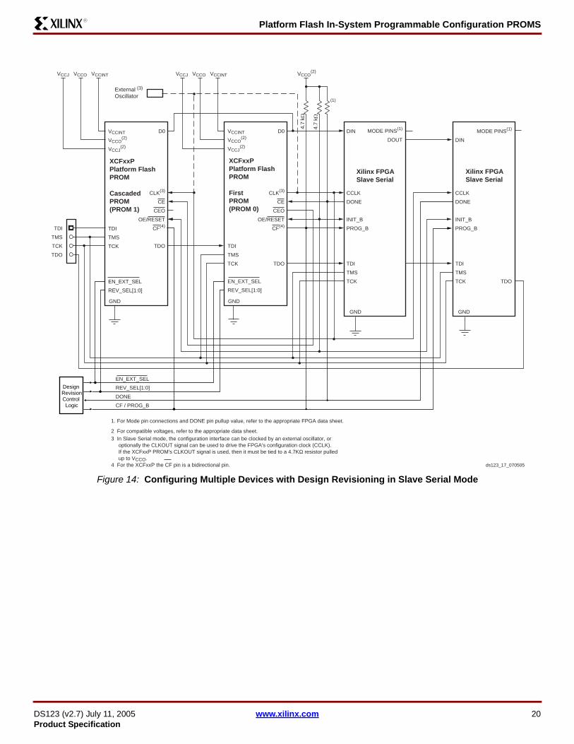
Platform Flash In-System Programmable Configuration PROMS
DS123 (v27) July 11 2005 wwwxilinxcom 20Product Specification
R
Figure 14 Configuring Multiple Devices with Design Revisioning in Slave Serial Mode
XCFxxPPlatform Flash PROM
First PROM(PROM 0)
VCCINT
VCCO(2)
VCCJ(2)
TDI
TMS
TCK
EN_EXT_SEL
REV_SEL[10]
D0
CLK(3)
CE
CEO
OERESET
CF(4)
TDO
Xilinx FPGASlave Serial
DIN
CCLK
DONE
INIT_B
PROG_B
TDI
TMS
TCK
VCCJ VCCO VCCINT
47
kΩ
47
kΩ
(1)
VCCO(2)
TDI
TMS
TCK
TDO
1 For Mode pin connections and DONE pin pullup value refer to the appropriate FPGA data sheet
2 For compatible voltages refer to the appropriate data sheet3 In Slave Serial mode the configuration interface can be clocked by an external oscillator or optionally the CLKOUT signal can be used to drive the FPGAs configuration clock (CCLK) If the XCFxxP PROMs CLKOUT signal is used then it must be tied to a 47KΩ resistor pulled up to VCCO4 For the XCFxxP the CF pin is a bidirectional pin
XCFxxPPlatform Flash PROM
Cascaded PROM(PROM 1)
VCCINT
VCCO(2)
VCCJ(2)
TDI
TMS
TCK
EN_EXT_SEL
REV_SEL[10]
D0
CLK(3)
CE
CEO
OERESET
CF(4)
TDO
VCCJ VCCO VCCINT
ds123_17_070505
Design RevisionControl Logic
EN_EXT_SEL
REV_SEL[10]
DONE
CF PROG_B
Xilinx FPGASlave Serial
DIN
CCLK
DONE
INIT_B
PROG_B
TDI
TMS
TCK
MODE PINS(1)
TDO
GNDGND
GND
DOUT
MODE PINS(1)
GND
External (3)
Oscillator
Platform Flash In-System Programmable Configuration PROMS
DS123 (v27) July 11 2005 wwwxilinxcom 21Product Specification
R
Figure 15 Configuring Multiple Devices with Design Revisioning in Slave SelectMAP Mode
XCFxxPPlatform Flash PROM
First PROM(PROM 0)
VCCINT
VCCO(2)
VCCJ(2)
TDI
TMS
TCK
EN_EXT_SEL
REV_SEL[10]
GND
D[07]
CLK(5)
CE
CEO
OERESET
CF(6)
BUSY(4)
TDO
Xilinx FPGASlave SelectMAP
D[07]
CCLK
DONE
INIT_B
PROG_B
BUSY(4)
TDI
TMS
TCK
MODE PINS(1)
RDWR_B
CS_B
TDO
VCCJ VCCO VCCINT
47
kΩ
47
kΩ
(1)
VCCO(2)
TDI
TMS
TCK
TDO
Notes
1 For Mode pin connections and DONE pin pullup value refer to the appropriate FPGA data sheet
2 For compatible voltages refer to the appropriate data sheet
3 RDWR_B (or WRITE) must be either driven Low or pulled down exernally One option is shown
4 The BUSY pin is only available with the XCFxxP Platform Flash PROM and the connection is only required for high frequency SelectMAP mode configuration For BUSY pin requirements refer to the appropriate FPGA data sheet
5 In Slave SelectMAP mode the configuration interface can be clocked by an external oscillator or optionally the CLKOUT signal can be used to drive the FPGAs configuration clock (CCLK) If the XCFxxP PROMs CLKOUT signal is used then it must be tied to a 47KΩ resistor pulled up to VCCO6 For the XCFxxP the CF pin is a bidirectional pin
Xilinx FPGASlave SelectMAP
D[07]
CCLK
DONE
INIT_B
PROG_B
BUSY(4)
TDI
TMS
TCK
MODE PINS(1)
RDWR_B
CS_B
TDO
XCFxxPPlatform Flash PROM
Cascaded PROM(PROM 1)
VCCINT
VCCO(2)
VCCJ(2)
TDI
TMS
TCK
EN_EXT_SEL
REV_SEL[10]
GND
D[07]
CLK(5)
CE
CEO
OERESET
CF(6)
BUSY(4)
TDO
VCCJ VCCO VCCINT
1KΩ
IO(3)
1KΩ
IO(3)
EN_EXT_SEL
REV_SEL[10]
CF
DONE
PROG_B
CS_B[10]
Design
Revision
Control
Logic
GND GND
ds123_18_070505
External (5)
Oscillator
Platform Flash In-System Programmable Configuration PROMS
DS123 (v27) July 11 2005 wwwxilinxcom 22Product Specification
R
Reset and Power-On Reset ActivationAt power up the device requires the VCCINT power supplyto monotonically rise to the nominal operating voltage withinthe specified VCCINT rise time If the power supply cannotmeet this requirement then the device might not performpower-on reset properly During the power-up sequenceOERESET is held Low by the PROM Once the requiredsupplies have reached their respective POR (Power OnReset) thresholds the OERESET release is delayed (TOERminimum) to allow more margin for the power supplies tostabilize before initiating configuration The OERESET pinis connected to an external 47kΩ pull-up resistor and alsoto the target FPGAs INIT pin For systems utilizing slow-ris-ing power supplies an additional power monitoring circuitcan be used to delay the target configuration until the sys-tem power reaches minimum operating voltages by holdingthe OERESET pin Low When OERESET is released theFPGArsquos INIT pin is pulled High allowing the FPGAs config-uration sequence to begin If the power drops below the
power-down threshold (VCCPD) the PROM resets andOERESET is again held Low until the after the POR thresh-old is reached OERESET polarity is not programmableThese power-up requirements are shown graphically inFigure 16For a fully powered Platform Flash PROM a reset occurswhenever OERESET is asserted (Low) or CE is deas-serted (High) The address counter is reset CEO is drivenHigh and the remaining outputs are placed in a high-imped-ance stateNotes1 The XCFxxS PROM only requires VCCINT to rise above
its POR threshold before releasing OERESET 2 The XCFxxP PROM requires both VCCINT to rise above
its POR threshold and for VCCO to reach the recommended operating voltage level before releasing OERESET
IO Input Voltage Tolerance and Power Sequencing The IOs on each re-programmable Platform Flash PROMare fully 33V-tolerant This allows 3V CMOS signals to con-nect directly to the inputs without damage The core powersupply (VCCINT) JTAG pin power supply (VCCJ) outputpower supply (VCCO) and external 3V CMOS IO signalscan be applied in any order Additionally for the XCFxxS PROM only when VCCO is sup-plied at 25V or 33V and VCCINT is supplied at 33V theIOs are 5V-tolerant This allows 5V CMOS signals to con-nect directly to the inputs on a powered XCFxxS PROMwithout damage Failure to power the PROM correctly whilesupplying a 5V input signal may result in damage to theXCFxxS device
Standby ModeThe PROM enters a low-power standby mode whenever CEis deasserted (High) In standby mode the address counteris reset CEO is driven High and the remaining outputs areplaced in a high-impedance state regardless of the state ofthe OERESET input For the device to remain in thelow-power standby mode the JTAG pins TMS TDI andTDO must not be pulled Low and TCK must be stopped(High or Low)When using the FPGA DONE signal to drive the PROM CEpin High to reduce standby power after configuration anexternal pull-up resistor should be used Typically a 330Ωpull-up resistor is used but refer to the appropriate FPGAdata sheet for the recommended DONE pin pull-up value Ifthe DONE circuit is connected to an LED to indicate FPGA
Figure 16 Platform Flash PROM Power-Up Requirements
TOER
VCCINT
VCCPOR
VCCPD
200 micros ramp50 ms ramp
TOER TRST
TIME (ms)
A slow-ramping VCCINT supply may still be below the minimum operating voltage when OERESET is released In this case the configuration sequence must be delayed until both VCCINT and VCCO have reached their recommended operating conditions
Recommended Operating Range
Delay or RestartConfiguration
ds123_21_103103
Platform Flash In-System Programmable Configuration PROMS
DS123 (v27) July 11 2005 wwwxilinxcom 23Product Specification
R
configuration is complete and is also connected to thePROM CE pin to enable low-power standby mode then anexternal buffer should be used to drive the LED circuit to
ensure valid transitions on the PROMrsquos CE pin If low-powerstandby mode is not required for the PROM then the CE pinshould be connected to ground
DC Electrical CharacteristicsThis data sheet is a Preliminary data sheet The DC characteristics are based on characterization rather than simulationFurther characteristic changes are not expected
bullAbsolute Maximum Ratings page 24bullSupply Voltage Requirements for Power-On Reset and Power-Down page 24bullRecommended Operating Conditions page 25bullQuality and Reliability Characteristics page 25bullDC Characteristics Over Operating Conditions page 26
Table 9 Truth Table for XCFxxS PROM Control InputsControl Inputs
Internal Address
Outputs
OERESET CE DATA CEO ICC
High LowIf address lt TC(2) increment Active High Active
If address = TC(2) dont change High-Z Low Reduced
Low Low Held reset High-Z High Active
X(1) High Held reset High-Z High Standby
Notes 1 X = donrsquot care2 TC = Terminal Count = highest address value TC + 1 = address 0
Table 10 Truth Table for XCFxxP PROM Control InputsControl Inputs
Internal Address
Outputs
OERESET CE CF BUSY(5) DATA CEO CLKOUT ICC
High Low High Low
If address lt TC(2) and address lt EA(3) increment Active High Active Active
If address lt TC(2) and address = EA(3) dont change High-Z High High-Z Reduced
Else If address = TC(2) dont change High-Z Low High-Z Reduced
High Low High High Unchanged Active and Unchanged High Active Active
High Low uarr X(1) Reset(4) Active High Active Active
Low Low X X Held reset(4) High-Z High High-Z Active
X High X X Held reset(4) High-Z High High-Z Standby
Notes 1 X = donrsquot care2 TC = Terminal Count = highest address value TC + 1 = address 03 For the XCFxxP with Design Revisioning enabled EA = end address (last address in the selected design revision) 4 For the XCFxxP with Design Revisioning enabled Reset = address reset to the beginning address of the selected bank If Design Revisioning is not
enabled then Reset = address reset to address 05 The BUSY input is only enabled when the XCFxxP is programmed for parallel data output and decompression is not enabled
Platform Flash In-System Programmable Configuration PROMS
DS123 (v27) July 11 2005 wwwxilinxcom 24Product Specification
R
AC Electrical CharacteristicsThis data sheet is a Preliminary data sheet The AC characteristics are based on characterization rather than simulationFurther characteristic changes are not expected
bullAC Characteristics Over Operating Conditions page 28bullAC Characteristics Over Operating Conditions When Cascading page 32
Absolute Maximum Ratings
Supply Voltage Requirements for Power-On Reset and Power-Down
Symbol DescriptionXCF01S XCF02S
XCF04SXCF08P XCF16P
XCF32P Units
VCCINT Internal supply voltage relative to GND ndash05 to +40 ndash05 to +27 V
VCCO IO supply voltage relative to GND ndash05 to +40 ndash05 to +40 V
VCCJ JTAG IO supply voltage relative to GND ndash05 to +40 ndash05 to +40 V
VIN Input voltage with respect to GNDVCCO lt 25V ndash05 to +36 ndash05 to +36 V
VCCO ge 25V ndash05 to +55 ndash05 to +36 V
VTS Voltage applied to High-Z outputVCCO lt 25V ndash05 to +36 ndash05 to +36 V
VCCO ge 25V ndash05 to +55 ndash05 to +36 V
TSTG Storage temperature (ambient) ndash65 to +150 ndash65 to +150 degC
TJ Junction temperature +125 +125 degC
Notes 1 Maximum DC undershoot below GND must be limited to either 05V or 10 mA whichever is easier to achieve During transitions the device pins can
undershoot to ndash20V or overshoot to +70V provided this over- or undershoot lasts less then 10 ns and with the forcing current being limited to 200 mA
2 Stresses beyond those listed under Absolute Maximum Ratings might cause permanent damage to the device These are stress ratings only and functional operation of the device at these or any other conditions beyond those listed under Operating Conditions is not implied Exposure to Absolute Maximum Ratings conditions for extended periods of time adversely affects device reliability
3 For soldering guidelines see the information on Packaging and Thermal Characteristics at wwwxilinxcom
Symbol Description
XCF01S XCF02S XCF04S
XCF08P XCF16P XCF32P
UnitsMin Max Min Max
TVCC VCCINT rise time from 0V to nominal voltage(2) 02 50 02 50 ms
VCCPOR POR threshold for the VCCINT supply 1 - 05 - V
TOER OERESET release delay following POR(3) 05 3 05 30 ms
VCCPD Power-down threshold for VCCINT supply - 1 - 05 V
TRSTTime required to trigger a device reset when the VCCINT supply drops below the maximum VCCPD threshold 10 - 10 - ms
Notes 1 VCCINT VCCO and VCCJ supplies may be applied in any order2 At power up the device requires the VCCINT power supply to monotonically rise to the nominal operating voltage within the specified TVCC rise time
If the power supply cannot meet this requirement then the device might not perform power-on-reset properly See Figure 16 page 223 If the VCCINT and VCCO supplies do not reach their respective recommended operating conditions before the OERESET pin is released then the
configuration data from the PROM will not be available at the recommended threshold levels The configuration sequence must be delayed until both VCCINT and VCCO have reached their recommended operating conditions
huffman
XCF08P
huffman
XCF08P
Platform Flash In-System Programmable Configuration PROMS
DS123 (v27) July 11 2005 wwwxilinxcom 25Product Specification
R
Recommended Operating Conditions
Quality and Reliability Characteristics
Symbol Description
XCF01S XCF02S XCF04S XCF08P XCF16P XCF32P
UnitsMin Typ Max Min Typ MaxVCCINT Internal voltage supply 30 33 36 165 18 20 V
VCCOSupply voltage for output drivers
33V Operation 30 33 36 30 33 36 V
25V Operation 23 25 27 23 25 27 V
18V Operation 17 18 19 17 18 19 V
15V Operation - - - TBD 15 TBD V
VCCJSupply voltage for JTAG output drivers
33V Operation 30 33 36 30 33 36 V
25V Operation 23 25 27 23 25 27 V
VILLow-level input voltage
33V Operation 0 - 08 0 - 08 V
25V Operation 0 - 08 0 - 08 V
18V Operation - - 20 VCCO - - 20 VCCO V
15V Operation - - - 0 - TBD V
VIHHigh-level input voltage
33V Operation 20 - 55 20 - 36 V
25V Operation 17 - 55 17 - 36 V
18V Operation 70 VCCO - 36 70 VCCO - 36 V
15V Operation - - - TBD - 36 V
TIN Input signal transition time(1) - - 500 - - 500 ns
VO Output voltage 0 - VCCO 0 - VCCO V
TA Operating ambient temperature ndash40 - 85 ndash40 - 85 degC
Notes 1 Input signal transition time measured between 10 VCCO and 90 VCCO
Symbol Description Min Max Units
TDR Data retention 20 - Years
NPE Programerase cycles (Endurance) 20000 - Cycles
VESD Electrostatic discharge (ESD) 2000 - Volts
huffman
XCF08P
huffman
18
Platform Flash In-System Programmable Configuration PROMS
DS123 (v27) July 11 2005 wwwxilinxcom 26Product Specification
R
DC Characteristics Over Operating Conditions
Symbol Description
XCF01S XCF02S XCF04S
XCF08P XCF16P XCF32P
UnitsTest
Conditions Min MaxTest
Conditions Min Max
VOH
High-level output voltage for 33V outputs IOH = ndash4 mA 24 - IOH = ndash4 mA 24 - V
High-level output voltage for 25V outputs IOH = ndash500 microA VCCO ndash 04
- IOH = ndash500 microA VCCO ndash 04
- V
High-level output voltage for 18V outputs IOH = ndash50 microA VCCO ndash 04
- IOH = ndash50 microA VCCO ndash 04
- V
High-level output voltage for 15V outputs - - - IOH = TBD TBD - V
VOL
Low-level output voltage for 33V outputs IOL = 4 mA - 04 IOL = 4 mA - 04 V
Low-level output voltage for 25V outputs IOL = 500 microA - 04 IOL = 500 microA - 04 V
Low-level output voltage for 18V outputs IOL = 50 microA - 04 IOL = 50 microA - 04 V
Low-level output voltage for 15V outputs - - - IOL = TBD - TBD V
ICCINT Internal voltage supply current active mode 33 MHz - 10 33 MHz - 10 mA
ICCO(1)
Output driver supply current active serial mode 33 MHz - 10 33 MHz - 10 mA
Output driver supply current active parallel mode - - - 33 MHz - 40 mA
ICCJ JTAG supply current active mode Note (2) - 5 Note (2) - 5 mA
ICCINTS Internal voltage supply current standby mode Note (3) - 5 Note (3) - 5 mA
ICCOS Output driver supply current standby mode Note (3) - 1 Note (3) - 1 mA
ICCJS JTAG supply current standby mode Note (3) - 1 Note (3) - 1 mA
IILJ JTAG pins TMS TDI and TDO pull-up current VCCJ = maxVIN = GND - 100 VCCJ = max
VIN = GND - 100 microA
IIL Input leakage current
VCCINT = maxVCCO = maxVIN = GND or
VCCO
ndash10 10
VCCINT = maxVCCO = maxVIN = GND or
VCCO
ndash10 10 microA
IIH Input and output High-Z leakage current
VCCINT = maxVCCO = maxVIN = GND or
VCCO
ndash10 10
VCCINT = maxVCCO = maxVIN = GND or
VCCO
ndash10 10 microA
IILPSource current through internal pull-ups onEN_EXT_SEL REV_SEL0 REV_SEL1
- - -
VCCINT = maxVCCO = maxVIN = GND or
VCCO
- 100 microA
IIHP Sink current through internal pull-down on BUSY - - -
VCCINT = maxVCCO = maxVIN = GND or
VCCO
-100 - microA
huffman
XCF08P
Platform Flash In-System Programmable Configuration PROMS
DS123 (v27) July 11 2005 wwwxilinxcom 27Product Specification
R
CIN Input capacitance VIN = GNDf = 10 MHz - 8 VIN = GND
f = 10 MHz - 8 pF
COUT Output capacitance VIN = GNDf = 10 MHz - 14 VIN = GND
f = 10 MHz - 14 pF
Notes 1 Output driver supply current specification based on no load conditions2 TDITMSTCK non-static (active)3 CE High OE Low and TMSTDITCK static
Symbol Description
XCF01S XCF02S XCF04S
XCF08P XCF16P XCF32P
UnitsTest
Conditions Min MaxTest
Conditions Min Max
huffman
XCF08P
Platform Flash In-System Programmable Configuration PROMS
DS123 (v27) July 11 2005 wwwxilinxcom 28Product Specification
R
AC Characteristics Over Operating Conditions
Symbol Description
XCF01S XCF02S XCF04S
XCF08P XCF16P XCF32P
UnitsMin Max Min Max
TOEOERESET to data delay(6) when VCCO = 33V or 25V - 10 - 25 ns
OERESET to data delay(6) when VCCO = 18V - 30 - 25 ns
TCECE to data delay(5) when VCCO = 33V or 25V - 15 - 25 ns
CE to data delay(5) when VCCO = 18V - 30 - 25 ns
TCACCLK to data delay(7) when VCCO = 33V or 25V - 15 - 25 ns
CLK to data delay(7) when VCCO = 18V - 30 - 25 ns
TOH
Data hold from CE OERESET or CLKwhen VCCO = 33V or 25V 0 - 5 - ns
Data hold from CE OERESET or CLKwhen VCCO = 18V 0 - 5 - ns
TDF
CE or OERESET to data float delay(2)
when VCCO = 33V or 25V - 25 - 45 ns
CE or OERESET to data float delay(2)
when VCCO = 18V - 30 - 45 ns
TCYC
Clock period(7) (serial mode) when VCCO = 33V or 25V 30 - 25 - ns
Clock period(7) (serial mode) when VCCO = 18V 67 - 25 - ns
Clock period(7) (parallel mode) when VCCO = 33V or 25V - - 30 - ns
Clock period(7) (parallel mode) when VCCO = 18V - - 30 - ns
CE
OERESET
CLK
CLKOUT(optional)
BUSY(optional)
DATA
TCE
TLC THC
TSCE
TOE TCAC
THCE
THOE
TCYC
TOH
TDFTOH
THBTSBTOEC
TCEC
TCLKO
TCOH
TCDD
CF
EN_EXT_SEL
REV_SEL[10]
TSXT THXT
TSRV THRV
ds123_22_110403
huffman
XCF08P
Platform Flash In-System Programmable Configuration PROMS
DS123 (v27) July 11 2005 wwwxilinxcom 29Product Specification
R
TLCCLK Low time(3) when VCCO = 33V or 25V 10 - 12 - ns
CLK Low time(3) when VCCO = 18V 15 - 12 - ns
THCCLK High time(3) when VCCO = 33V or 25V 10 - 12 - ns
CLK High time(3) when VCCO = 18V 15 - 12 - ns
TSCE
CE setup time to CLK (guarantees proper counting)(3)
when VCCO = 33V or 25V 20 - 30 - ns
CE setup time to CLK (guarantees proper counting)(3)
when VCCO = 18V 30 30 - ns
THCE
CE hold time (guarantees counters are reset)(5)
when VCCO = 33V or 25V 250 - 2000 - ns
CE hold time (guarantees counters are reset)(5)
when VCCO = 18V 250 - 2000 - ns
THOE
OERESET hold time (guarantees counters are reset)(6)
when VCCO = 33V or 25V 250 - 2000 - ns
OERESET hold time (guarantees counters are reset)(6)
when VCCO = 18V 250 - 2000 - ns
TSBBUSY setup time to CLK when VCCO = 33V or 25V - - 12 - ns
BUSY setup time to CLK when VCCO = 18V - - 12 - ns
THBBUSY hold time to CLK when VCCO = 33V or 25V - - 8 - ns
BUSY hold time to CLK when VCCO = 18V - - 8 - ns
TCLKO
CLK input to CLKOUT output delay when VCCO = 33V or 25V - - - 35 ns
CLK input to CLKOUT output delay when VCCO = 18V - - - 35 ns
CLK input to CLKOUT output delay when VCCO = 33V or 25V with decompression(12) - - - 35 ns
CLK input to CLKOUT output delay when VCCO = 18V with decompression(12) - - - 35 ns
TCEC
CE to CLKOUT delay(8) with CLKOUT sourced from internal oscillator when VCCO = 33V or 25V - - 0 1 micros
CE to CLKOUT delay(8) with CLKOUT sourced from internal oscillator when VCCO = 18V - - 0 1 micros
CE to CLKOUT delay(8) with CLKOUT sourced from external CLK input when VCCO = 33V or 25V - - 0 2 CLK
cycles -
CE to CLKOUT delay(8) with CLKOUT sourced from external CLK input when VCCO = 18V - - 0 2 CLK
cycles -
TOEC
OERESET to CLKOUT delay(8) with CLKOUT sourced from internal oscillator when VCCO = 33V or 25V - - 0 1 micros
OERESET to CLKOUT delay(8) with CLKOUT sourced from internal oscillator when VCCO = 18V - - 0 1 micros
OERESET to CLKOUT delay(8) with CLKOUT sourced from external CLK input when VCCO = 33V or 25V 0 2 CLK
cycles -
OERESET to CLKOUT delay(8) with CLKOUT sourced from external CLK input when VCCO = 18V 0 2 CLK
cycles -
Symbol Description
XCF01S XCF02S XCF04S
XCF08P XCF16P XCF32P
UnitsMin Max Min Max
huffman
XCF08P
Platform Flash In-System Programmable Configuration PROMS
DS123 (v27) July 11 2005 wwwxilinxcom 30Product Specification
R
TCDDCLKOUT to data delay when VCCO = 33V or 25V(9) - - - 22 ns
CLKOUT to data delay when VCCO = 18V(9) - - - 22 ns
TDDC
Data setup time to CLKOUT when VCCO = 33V or 25V with decompression(9)(12) - - 5 ns
Data setup time to CLKOUT when VCCO = 18V with decompression(9)(12) - - 5 ns
TCOH
Data hold from CLKOUT when VCCO = 33V or 25V - - 3 - ns
Data hold from CLKOUT when VCCO = 18V - - 3 - ns
Data hold from CLKOUT when VCCO = 33V or 25V with decompression(12) - - 3 - ns
Data hold from CLKOUT when VCCO = 18V with decompression(12) - - 3 - ns
TSXT
EN_EXT_SEL setup time to CF (rising edge)when VCCO = 33V or 25V - - 300 - ns
EN_EXT_SEL setup time to CF (rising edge)when VCCO = 18V - - 300 - ns
THXT
EN_EXT_SEL hold time from CF (rising edge)when VCCO = 33V or 25V - - 300 - ns
EN_EXT_SEL hold time from CF (rising edge)when VCCO = 18V - - 300 - ns
TSRV
REV_SEL setup time to CF (rising edge)when VCCO = 33V or 25V - - 300 - ns
REV_SEL setup time to CF (rising edge)when VCCO = 18V - - 300 - ns
THRV
REV_SEL hold time from CF (rising edge)when VCCO = 33V or 25V - - 300 - ns
REV_SEL hold time from CF (rising edge)when VCCO = 18V - - 300 - ns
FF
CLKOUT default (fast) frequency(10) - - 25 50 MHz
CLKOUT default (fast) frequency with decompression(12) - - 125 25 MHz
Symbol Description
XCF01S XCF02S XCF04S
XCF08P XCF16P XCF32P
UnitsMin Max Min Max
huffman
XCF08P
Platform Flash In-System Programmable Configuration PROMS
DS123 (v27) July 11 2005 wwwxilinxcom 31Product Specification
R
FS
CLKOUT alternate (slower) frequency(11) - - 125 25 MHz
CLKOUT alternate (slower) frequency with decompression(12) - - 6 125 MHz
Notes 1 AC test load = 50 pF for XCF01SXCF02SXCF04S 30 pF for XCF08PXCF16PXCF32P2 Float delays are measured with 5 pF AC loads Transition is measured at plusmn200 mV from steady-state active levels3 Guaranteed by design not tested4 All AC parameters are measured with VIL = 00V and VIH = 30V5 If THCE High lt 2 micros TCE = 2 micros6 If THOE Low lt 2 micros TOE = 2 micros7 This is the minimum possible TCYC Actual TCYC = TCAC + FPGA Data setup time
Example With the XCF32P in serial mode with VCCO at 33V if FPGA Data setup time = 15 ns then the actual TCYC = 25 ns +15 ns = 40 ns8 The delay before the enabled CLKOUT signal begins clocking data out of the device is dependent on the clocking configuration The delay before
CLKOUT is enabled will increase if decompression is enabled 9 Slower CLK frequency option may be required to meet the FPGA data sheet setup time10 Typical CLKOUT default (fast) period = 25 ns (40 MHz)11 Typical CLKOUT alternate (slower) period = 50 ns (20 MHz)12 When decompression is enabled the CLKOUT signal becomes a controlled clock output When decompressed data is available CLKOUT will toggle
at frac12 the source clock frequency (either frac12 the selected internal clock frequency or frac12 the external CLK input frequency) When decompressed data is not available the CLKOUT pin is parked High If CLKOUT is used then it must be pulled High externally using a 47kΩ pull-up to VCCO
Symbol Description
XCF01S XCF02S XCF04S
XCF08P XCF16P XCF32P
UnitsMin Max Min Max
huffman
XCF08P
huffman
XCF08P
Platform Flash In-System Programmable Configuration PROMS
DS123 (v27) July 11 2005 wwwxilinxcom 32Product Specification
R
AC Characteristics Over Operating Conditions When Cascading
Symbol Description
XCF01S XCF02S XCF04S
XCF08P XCF16P XCF32P
UnitsMin Max Min Max
TCDF
CLK to output float delay(23) when VCCO = 25V or 33V - 25 - 20 ns
CLK to output float delay(23) when VCCO = 18V - 35 - 20 ns
TOCKCLK to CEO delay(35) when VCCO = 25V or 33V - 20 - 20 ns
CLK to CEO delay(35) when VCCO = 18V - 35 - 20 ns
TOCECE to CEO delay(36) when VCCO = 25V or 33V - 20 - 80 ns
CE to CEO delay(36) when VCCO = 18V - 35 - 80 ns
TOOEOERESET to CEO delay(3) when VCCO = 25V or 33V - 20 - 80 ns
OERESET to CEO delay(3) when VCCO = 18V - 35 - 80 ns
TCOCECLKOUT to CEO delay when VCCO = 25V or 33V - - - 20 ns
CLKOUT to CEO delay when VCCO = 18V - - - 20 ns
TCODF
CLKOUT to output float delay when VCCO = 25V or 33V - - - 25 ns
CLKOUT to output float delay when VCCO = 18V - - - 25 ns
Notes 1 AC test load = 50 pF for XCF01SXCF02SXCF04S 30 pF for XCF08PXCF16PXCF32P2 Float delays are measured with 5 pF AC loads Transition is measured at plusmn200 mV from steady state active levels3 Guaranteed by design not tested4 All AC parameters are measured with VIL = 00V and VIH = 30V5 For cascaded PROMs if the FPGArsquos dual-purpose configuration data pins are set to persist as configuration pins the minimum period is increased
based on the CLK to CEO and CE to data propagation delays- TCYC minimum = TOCK + TCE + FPGA Data setup time- TCAC maximum = TOCK + TCE
6 For cascaded PROMs if the FPGArsquos dual-purpose configuration data pins become general IO pins after configuration to allow for the disable to propagate to the cascaded PROMs and to avoid contention on the data lines following configuration the minimum period is increased based on the CE to CEO and CE to data propagation delays- TCYC minimum = TOCE + TCE - TCAC maximum = TOCK + TCE
OERESET
CE
CLK
CLKOUT(optional)
DATA
CEO
TOCETOOE
First BitLast Bit
TCDFTCODF
TOCK TCOCE
ds123_23_102203
huffman
XCF08P
huffman
XCF08P
Platform Flash In-System Programmable Configuration PROMS
DS123 (v27) July 11 2005 wwwxilinxcom 33Product Specification
R
Pinouts and Pin DescriptionsThe XCFxxS Platform Flash PROM is available in the VO20 and VOG20 packages The XCFxxP Platform Flash PROM isavailable in the VO48 VOG48 FS48 and FSG48 packages This section includes
bull Table 11 XCFxxS Pin Names and Descriptions page 33bull Figure 17 VO20VOG20 Pinout Diagram (Top View) with Pin Names page 34bull Table 12 XCFxxP Pin Names and Descriptions page 35bull Figure 18 VO48VOG48 Pinout Diagram (Top View) with Pin Names page 36bull Table 13 FS48FSG48 Pin NumberName Reference page 38bull Figure 19 FS48FSG48 Pinout Diagram (Top View) page 38
Notes 1 VO20VOG20 denotes a 20-pin (TSSOP) Plastic Thin Shrink Small Outline Package 2 VO48VOG48 denotes a 48-pin (TSOP) Plastic Thin Small Outline Package3 FS48FSG48 denotes a 48-pin (TFBGA) Plastic Thin Fine Pitch Ball Grid Array (08 mm pitch)
XCFxxS Pinouts and Pin DescriptionsTable 11 provides a list of the pin names and descriptions for the XCFxxS 20-pin VO20VOG20 package
Table 11 XCFxxS Pin Names and Descriptions
Pin NameBoundary
Scan OrderBoundary
Scan Function Pin Description20-pin TSSOP (VO20VOG20)
D04 Data Out D0 is the DATA output pin to provide data for configuring an
FPGA in serial mode The D0 output is set to a high-impedance state during ISPEN (when not clamped)
13 Output Enable
CLK 0 Data InConfiguration Clock Input Each rising edge on the CLK input increments the internal address counter if the CLK input is selected CE is Low and OERESET is High
3
OERESET
20 Data In Output EnableReset (Open-Drain IO) When Low this input holds the address counter reset and the DATA output is in a high-impedance state This is a bidirectional open-drain pin that is held Low while the PROM is reset Polarity is not programmable
819 Data Out
18 Output Enable
CE 15 Data InChip Enable Input When CE is High the device is put into low-power standby mode the address counter is reset and the DATA pins are put in a high-impedance state
10
CF22 Data Out Configuration Pulse (Open-Drain Output) Allows JTAG
CONFIG instruction to initiate FPGA configuration without powering down FPGA This is an open-drain output that is pulsed Low by the JTAG CONFIG command
721 Output Enable
CEO
12 Data OutChip Enable Output Chip Enable Output (CEO) is connected to the CE input of the next PROM in the chain This output is Low when CE is Low and OERESET input is High AND the internal address counter has been incremented beyond its Terminal Count (TC) value CEO returns to High when OERESET goes Low or CE goes High
13
11 Output Enable
TMS Mode Select
JTAG Mode Select Input The state of TMS on the rising edge of TCK determines the state transitions at the Test Access Port (TAP) controller TMS has an internal 50KΩ resistive pull-up to VCCJ to provide a logic 1 to the device if the pin is not driven
5
TCK ClockJTAG Clock Input This pin is the JTAG test clock It sequences the TAP controller and all the JTAG test and programming electronics
6
Platform Flash In-System Programmable Configuration PROMS
DS123 (v27) July 11 2005 wwwxilinxcom 34Product Specification
R
XCFxxS Pinout Diagram
TDI Data In
JTAG Serial Data Input This pin is the serial input to all JTAG instruction and data registers TDI has an internal 50KΩ resistive pull-up to VCCJ to provide a logic 1 to the device if the pin is not driven
4
TDO Data Out
JTAG Serial Data Output This pin is the serial output for all JTAG instruction and data registers TDO has an internal 50KΩ resistive pull-up to VCCJ to provide a logic 1 to the system if the pin is not driven
17
VCCINT +33V Supply Positive 33V supply voltage for internal logic 18
VCCO+33V 25V or 18V IO Supply Positive 33V 25V or 18V supply voltage connected to the output voltage drivers and input buffers
19
VCCJ+33V or 25V JTAG IO Supply Positive 33V 25V or 18V supply voltage connected to the TDO output voltage driver and TCK TMS and TDI input buffers
20
GND Ground 11
DNC Do not connect (These pins must be left unconnected) 2 9 12 14 15 16
Figure 17 VO20VOG20 Pinout Diagram (Top View) with Pin Names
Table 11 XCFxxS Pin Names and Descriptions (Continued)
Pin NameBoundary
Scan OrderBoundary
Scan Function Pin Description20-pin TSSOP (VO20VOG20)
VO20VOG20Top View
ds123_02_071304
1
2
3
4
5
6
7
8
9
10
20
19
18
17
16
15
14
13
12
11
D0
(DNC)
CLK
TDI
TMS
TCK
CF
OERESET
(DNC)
CE
VCCJ
VCCO
VCCINT
TDO
(DNC)
(DNC)
CEO
(DNC)
GND
(DNC)
Platform Flash In-System Programmable Configuration PROMS
DS123 (v27) July 11 2005 wwwxilinxcom 35Product Specification
R
XCFxxP Pinouts and Pin DescriptionsTable 12 provides a list of the pin names and descriptions for the XCFxxP 48-pin VO48VOG48 and 48-pin FS48FSG48packages
Table 12 XCFxxP Pin Names and Descriptions
Pin Name
Boundary Scan Order
Boundary Scan
Function Pin Description
48-pin TSOP (VO48VOG48)
48-pin TFBGA (FS48FSG48)
D028 Data Out
D0 is the DATA output pin to provide data for configuring an FPGA in serial mode D0-D7 are the DATA output pins to provide parallel data for configuring a Xilinx FPGA in SelectMap (parallel) mode The D0 output is set to a high-impedance state during ISPEN (when not clamped)The D1-D7 outputs are set to a high-impedance state during ISPEN (when not clamped) and when serial mode is selected for configuration The D1-D7 pins can be left unconnected when the PROM is used in serial mode
28 H627 Output Enable
D126 Data Out
29 H525 Output Enable
D224 Data Out
32 E523 Output Enable
D322 Data Out
33 D521 Output Enable
D420 Data Out
43 C519 Output Enable
D518 Data Out
44 B517 Output Enable
D616 Data Out
47 A515 Output Enable
D714 Data Out
48 A613 Output Enable
CLK 01 Data In
Configuration Clock Input An internal programmable control bit selects between the internal oscillator and the CLK input pin as the clock source to control the configuration sequence Each rising edge on the CLK input increments the internal address counter if the CLK input is selected CE is Low OERESET is High BUSY is Low (parallel mode only) and CF is High
12 B3
OERESET
04 Data In Output EnableReset (Open-Drain IO)When Low this input holds the address counter reset and the DATA and CLKOUT outputs are placed in a high-impedance state This is a bidirectional open-drain pin that is held Low while the PROM is reset Polarity is not programmable
11 A303 Data Out
02 Output Enable
CE 00 Data In
Chip Enable Input When CE is High the device is put into low-power standby mode the address counter is reset and the DATA and CLKOUT outputs are placed in a high-impedance state
13 B4
CF
11 Data InConfiguration Pulse (Open-Drain IO) As an output this pin allows the JTAG CONFIG instruction to initiate FPGA configuration without powering down the FPGA This is an open-drain signal that is pulsed Low by the JTAG CONFIG command As an input on the rising edge of CF the current design revision selection is sampled and the internal address counter is reset to the start address for the selected revision If unused the CF pin should be pulled High using an external 47KΩ pull-up to VCCO
6 D110 Data Out
09 Output Enable
Platform Flash In-System Programmable Configuration PROMS
DS123 (v27) July 11 2005 wwwxilinxcom 36Product Specification
R
CEO
06 Data OutChip Enable Output Chip Enable Output (CEO) is connected to the CE input of the next PROM in the chain This output is Low when CE is Low and OERESET input is High AND the internal address counter has been incremented beyond its Terminal Count (TC) value CEO returns to High when OERESET goes Low or CE goes High
10 D2
05 Output Enable
EN_EXT_SEL 31 Data In
Enable External Selection Input When this pin is Low design revision selection is controlled by the Revision Select pins When this pin is High design revision selection is controlled by the internal programmable Revision Select control bits EN_EXT_SEL has an internal 50KΩ resistive pull-up to VCCO to provide a logic 1 to the device if the pin is not driven
25 H4
REV_SEL0 30 Data InRevision Select[10] Inputs When the EN_EXT_SEL is Low the Revision Select pins are used to select the design revision to be enabled overriding the internal programmable Revision Select control bits The Revision Select[10] inputs have an internal 50KΩ resistive pull-up to VCCO to provide a logic 1 to the device if the pins are not driven
26 G3
REV_SEL1 29 Data In 27 G4
BUSY 12 Data In
Busy Input The BUSY input is enabled when parallel mode is selected for configuration When BUSY is High the internal address counter stops incrementing and the current data remains on the data pins On the first rising edge of CLK after BUSY transitions from High to Low the data for the next address is driven on the data pins When serial mode or decompression is enabled during device programming the BUSY input is disabled BUSY has an internal 50KΩ resistive pull-down to GND to provide a logic 0 to the device if the pin is not driven
5 C1
CLKOUT
08 Data Out
Configuration Clock Output An internal Programmable control bit enables the CLKOUT signal which is sourced from either the internal oscillator or the CLK input pin Each rising edge of the selected clock source increments the internal address counter if data is available CE is Low and OERESET is High Output data is available on the rising edge of CLKOUT CLKOUT is disabled if CE is High or OERESET is Low If decompression is enabled CLKOUT is parked High when decompressed data is not ready When CLKOUT is disabled the CLKOUT pin is put into a high-Z state If CLKOUT is used then it must be pulled High externally using a 47KΩ pull-up to VCCO
9 C2
07 Output Enable
TMS Mode Select
JTAG Mode Select Input The state of TMS on the rising edge of TCK determines the state transitions at the Test Access Port (TAP) controller TMS has an internal 50KΩ resistive pull-up to VCCJ to provide a logic 1 to the device if the pin is not driven
21 E2
TCK ClockJTAG Clock Input This pin is the JTAG test clock It sequences the TAP controller and all the JTAG test and programming electronics
20 H3
TDI Data In
JTAG Serial Data Input This pin is the serial input to all JTAG instruction and data registers TDI has an internal 50KΩ resistive pull-up to VCCJ to provide a logic 1 to the device if the pin is not driven
19 G1
Table 12 XCFxxP Pin Names and Descriptions (Continued)
Pin Name
Boundary Scan Order
Boundary Scan
Function Pin Description
48-pin TSOP (VO48VOG48)
48-pin TFBGA (FS48FSG48)
Platform Flash In-System Programmable Configuration PROMS
DS123 (v27) July 11 2005 wwwxilinxcom 37Product Specification
R
XCFxxP Pinout Diagrams
Figure 18 VO48VOG48 Pinout Diagram (Top View) with Pin Names
TDO Data Out
JTAG Serial Data Output This pin is the serial output for all JTAG instruction and data registers TDO has an internal 50KΩ resistive pull-up to VCCJ to provide a logic 1 to the system if the pin is not driven
22 E6
VCCINT +18V Supply Positive 18V supply voltage for internal logic 4 15 34
B1 E1 G6
VCCO+33V 25V or 18V IO Supply Positive 33V 25V or 18V supply voltage connected to the output voltage drivers and input buffers
8 30 38 45
B2 C6 D6 G5
VCCJ+33V or 25V JTAG IO Supply Positive 33V 25V or 18V supply voltage connected to the TDO output voltage driver and TCK TMS and TDI input buffers
24 H2
GND Ground2 7
17 23 31 36
46
A1 A2 B6 F1 F5 F6
H1
DNC Do Not Connect (These pins must be left unconnected)
1 3 14 16 18 35 37 39 40 41
42
A4 C3 C4 D3 D4 E3 E4 F2 F3 F4
G2
Table 12 XCFxxP Pin Names and Descriptions (Continued)
Pin Name
Boundary Scan Order
Boundary Scan
Function Pin Description
48-pin TSOP (VO48VOG48)
48-pin TFBGA (FS48FSG48)
123456789101112131415161718192021222324
484746454443424140393837363534333231302928272625
VO48VOG48Top View
DNCGNDDNC
VCCINTBUSY
CFGND
VCCOCLKOUT
CEOOERESET
CLKCE
DNCVCCINT
DNCGNDDNCTDI
TCKTMSTDOGND
D7D6GNDVCCOD5D4DNCDNCDNCDNCVCCODNCGNDDNCVCCINTD3D2GNDVCCOD1D0REV_SEL1REV_SEL0EN_EXT_SELVCCJ
Platform Flash In-System Programmable Configuration PROMS
DS123 (v27) July 11 2005 wwwxilinxcom 38Product Specification
R
Table 13 FS48FSG48 Pin NumberName ReferencePin
Number Pin NamePin
Number Pin NameA1 GND E1 VCCINT
A2 GND E2 TMS
A3 OERESET E3 DNC
A4 DNC E4 DNC
A5 D6 E5 D2
A6 D7 E6 TDO
B1 VCCINT F1 GND
B2 VCCO F2 DNC
B3 CLK F3 DNC
B4 CE F4 DNC
B5 D5 F5 GND
B6 GND F6 GND
C1 BUSY G1 TDI
C2 CLKOUT G2 DNC
C3 DNC G3 REV_SEL0
C4 DNC G4 REV_SEL1
C5 D4 G5 VCCO
C6 VCCO G6 VCCINT
D1 CF H1 GND
D2 CEO H2 VCCJ
D3 DNC H3 TCK
D4 DNC H4 EN_EXT_SEL
D5 D3 H5 D1
D6 VCCO H6 D0
Table 13 FS48FSG48 Pin NumberName ReferencePin
Number Pin NamePin
Number Pin Name
1 2 3 4 5 6
ds121_01_071604
A
B
C
D
E
F
G
H
FS48FSG48Top View
Platform Flash In-System Programmable Configuration PROMS
DS123 (v27) July 11 2005 wwwxilinxcom 39Product Specification
R
Ordering Information
Valid Ordering Combinations
Marking Information
XCF01SVO20 C XCF08PVO48 C XCF08PFS48 C XCF01SVOG20 C XCF08PVOG48 C XCF08PFSG48 C
XCF02SVO20 C XCF16PVO48 C XCF16PFS48 C XCF02SVOG20 C XCF16PVOG48 C XCF16PFSG48 C
XCF04SVO20 C XCF32PVO48 C XCF32PFS48 C XCF04SVOG20 C XCF32PVOG48 C XCF32PFSG48 C
XCF04S VO20 C
Operating RangeProcessingC = (TA = ndash40degC to +85degC)Package Type
VO20 = 20-pin TSSOP PackageVOG20 = 20-pin TSSOP Package Pb-free
Device NumberXCF01SXCF02SXCF04S
XCF32P FS48 C
Operating RangeProcessingC = (TA = ndash40degC to +85degC)Package Type
VO48 = 48-pin TSOP PackageVOG48 = 48-pin TSOP Package Pb-freeFS48 = 48-pin TFBGA PackageFSG48 = 48-pin TFBGA Package Pb-free
Device NumberXCF08PXCF16PXCF32P
XCF04S-V
Operating RangeProcessingC = (TA = ndash40degC to +85degC)Package Type
V = 20-pin TSSOP Package (VO20)VG = 20-pin TSSOP Package Pb-free (VOG20)VO48 = 48-pin TSOP Package (VO48)VOG48 = 48-pin TSOP Package Pb-free (VOG48)F48 = 48-pin TFBGA Package (FS48)FG48 = 48-pin TFBGA Package Pb-free (FSG48)
Device NumberXCF01SXCF02SXCF04SXCF08PXCF16PXCF32P
huffman
XCF08PFS48 C
huffman
XCF08P
huffman
XCF08P
Platform Flash In-System Programmable Configuration PROMS
DS123 (v27) July 11 2005 wwwxilinxcom 40Product Specification
R
Revision HistoryThe following table shows the revision history for this document
Date Version Revision
042903 10 Xilinx Initial Release
060303 11 Made edits to all pages
110503 20 Major revision
111803 21 Pinout corrections as followsbull Table 12
- For VO48 package removed 38 from VCCINT and added it to VCCO- For FS48 package removed pin D6 from VCCINT and added it to VCCO
bull Table 13 (FS48 package) - For pin D6 changed name from VCCINT to VCCO- For pin A4 changed name from GND to DNC
bull Figure 18 (VO48 package) For pin 38 changed name from VCCINT to VCCO
121503 22 bull Added specification (47kΩ) for recommended pull-up resistor on OERESET pin to section Reset and Power-On Reset Activation page 22
bull Added paragraph to section Standby Mode page 22 concerning use of a pull-up resistor andor buffer on the DONE pin
050704 23 bull Section Features page 1 Added package styles and 33 MHz configuration speed limit to itemized features
bull Section Description page 1 and following Added state conditions for CF and BUSY to the descriptive text
bull Table 2 page 3 Updated Virtex-II configuration bitstream sizesbull Section Design Revisioning page 9 Rewrittenbull Section PROM to FPGA Configuration Mode and Connections Summary
page 10 and following five instances Added instruction to tie CF High if it is not tied to the FPGArsquos PROG_B (PROGRAM) input
bull Figure 8 page 14 through Figure 15 page 21 Added footnote indicating the directionality of the CF pin in each configuration
bull Section IO Input Voltage Tolerance and Power Sequencing page 22 Rewrittenbull Table 10 page 23 Added CF column to truth table and added an additional row to
document the Low state of CFbull Section Absolute Maximum Ratings page 24 Revised VIN and VTS for rsquoPrsquo
devices bull Section Supply Voltage Requirements for Power-On Reset and Power-Down
page 24- Revised footnote callout number on TOER from Footnote (4) to Footnote (3)- Added Footnote (2) callout to TVCC
bull Section Recommended Operating Conditions page 25 - Added Typical (Typ) parameter columns and parameters for VCCINT and
VCCOVCCJ- Added 15V operation parameter row to VIL and VIH rsquoPrsquo devices- Revised VIH Min 25V operation from 20V to 17V- Added parameter row TIN and Max parameters
bull (Continued on next page)
Platform Flash In-System Programmable Configuration PROMS
DS123 (v27) July 11 2005 wwwxilinxcom 41Product Specification
R
050704(contrsquod)
23(contrsquod)
bull Section DC Characteristics Over Operating Conditions page 26 - Added parameter row and parameters for parallel configuration mode rsquoPrsquo
devices to ICCO- Added Footnote (1) and Footnote (2) with callouts in the Test Conditions column
for ICCJ ICCINTS ICCOS and ICCJS to define active and standby mode requirements
bull Section AC Characteristics Over Operating Conditions page 28 - Corrected description for second TCAC parameter line to show parameters for
18V VCCO- Revised Footnote (7) to indicate VCCO = 33V- Applied Footnote (7) to second TCYC parameter line
bull Section AC Characteristics Over Operating Conditions When Cascading page 32 Revised Footnote (5)TCYC Min and TCAC Min formulas
bull Table 12 page 35 - Added additional state conditions to CLK description- Added function of resetting the internal address counter to CF description
072004 24 bull Added Pb-free package options VOG20 FSG48 and VOG48bull Figure 8 page 14 and Figure 9 page 15 Corrected connection name for FPGA
DOUT (OPTIONAL Daisy-chained Slave FPGAs with different configurations) from DOUT to DIN
bull Section Absolute Maximum Ratings page 24 Removed parameter TSOL from table (TSOL information can be found in Package User Guide)
bull Table 2 page 3 Removed reference to XC2VP125 FPGA
101804 25 bull Table 1 page 1 Broke out VCCO VCCJ into two separate columnsbull Table 7 page 7 Added clarification of ID code die revision bitsbull Table 8 page 8 Deleted TCKMIN2 (bypass mode) and renamed TCKMIN1 to TCKMINbull Table Recommended Operating Conditions page 25 Separated VCCO and VCCJ
parametersbull Table DC Characteristics Over Operating Conditions page 26
- Added most parameter values for XCF08P XCF16P XCF32P devices- Added Footnote (1) to ICCO specifying no-load conditions
bull Table AC Characteristics Over Operating Conditions page 28 - Added most parameter values for XCF08P XCF16P XCF32P devices- Expanded Footnote (1) to include XCF08P XCF16P XCF32P devices- Added Footnote (8) through (11) relating to CLKOUT conditions for various
parameters- Added rows to TCYC specifying parameters for parallel mode- Added rows specifying parameters with decompression for TCLKO TCOH TFF
TSF- Added TDDC (setup time with decompression)
bull Table AC Characteristics Over Operating Conditions When Cascading page 32 - Added most parameter values for XCF08P XCF16P XCF32P devices- Separated Footnote (5) into Footnotes (5) and (6) to specify different
derivations of TCYC depending on whether dual-purpose configuration pins persist as configuration pins or become general IO pins after configuration
huffman
XCF08P
huffman
XCF08P
huffman
XCF08P
huffman
XCF08P
Platform Flash In-System Programmable Configuration PROMS
DS123 (v27) July 11 2005 wwwxilinxcom 42Product Specification
R
031405 26 bull Added Virtex-4 LXFXSX configuration data to Table 2 bull Corrected Virtex-II configuration data in Table 2bull Corrected Virtex-II Pro configuration data in Table 2bull Added Spartan-3L configuration data to Table 2bull Added Spartan-3E configuration data to Table 2bull Paragraph added to FPGA Master SelectMAP (Parallel) Mode (1) page 11bull Changes to DC Characteristics
- TOER changed page 26- IOL changed for VOL page 26- VCCO added to test conditions for IIL IILP IIHPand IIH page 26 Values modified
for IILP and IIHPbull Changes to AC Characteristics
- TLC and THC modified for 18V page 29- New rows added for TCEC and TOEC page 29
bull Minor changes to grammar and punctuationbull Add explanation of Preliminary to DC and AC Electrical Characteristics
071105 27 bull Move from Preliminary to Product Specificationbull Corrections to Virtex-4 configuration bitstream valuesbull Minor changes to figures 9 14 15 and 18bull Change to Internal Oscillator description page 8bull Change to CLKOUT description page 8
- Platform Flash In-System Programmable Configuration PROMS
-
- Features
- Description
- Programming
-
- In-System Programming
-
- OERESET
-
- External Programming
- Reliability and Endurance
-
- Design Security
-
- Read Protection
- Write Protection
-
- IEEE 11491 Boundary-Scan (JTAG)
-
- Instruction Register
-
- XCFxxS Instruction Register (8 bits wide)
- XCFxxP Instruction Register (16 bits wide)
-
- Boundary Scan Register
- Identification Registers
-
- IDCODE Register
- USERCODE Register
- Customer Code Register
-
- Platform Flash PROM TAP Characteristics
-
- TAP Timing
- TAP AC Parameters
-
- Additional Features for the XCFxxP
-
- Internal Oscillator
- CLKOUT
- Decompression
- Design Revisioning
-
- PROM to FPGA Configuration Mode and Connections Summary
-
- FPGA Master Serial Mode
- FPGA Slave Serial Mode
- Serial Daisy Chain
- FPGA Master SelectMAP (Parallel) Mode
- FPGA Slave SelectMAP (Parallel) Mode
- FPGA SelectMAP (Parallel) Device Chaining
- Cascading Configuration PROMs
- Initiating FPGA Configuration
-
- Configuration PROM to FPGA Device Interface Connection Diagrams
- Reset and Power-On Reset Activation
- IO Input Voltage Tolerance and Power Sequencing
- Standby Mode
- DC Electrical Characteristics
- AC Electrical Characteristics
-
- Absolute Maximum Ratings
- Supply Voltage Requirements for Power-On Reset and Power-Down
- Recommended Operating Conditions
- Quality and Reliability Characteristics
- DC Characteristics Over Operating Conditions
- AC Characteristics Over Operating Conditions
- AC Characteristics Over Operating Conditions When Cascading
-
- Pinouts and Pin Descriptions
-
- XCFxxS Pinouts and Pin Descriptions
- XCFxxS Pinout Diagram
- XCFxxP Pinouts and Pin Descriptions
- XCFxxP Pinout Diagrams
-
- Ordering Information
- Valid Ordering Combinations
- Marking Information
- Revision History
-
Platform Flash In-System Programmable Configuration PROMS
DS123 (v27) July 11 2005 wwwxilinxcom 24Product Specification
R
AC Electrical CharacteristicsThis data sheet is a Preliminary data sheet The AC characteristics are based on characterization rather than simulationFurther characteristic changes are not expected
bullAC Characteristics Over Operating Conditions page 28bullAC Characteristics Over Operating Conditions When Cascading page 32
Absolute Maximum Ratings
Supply Voltage Requirements for Power-On Reset and Power-Down
Symbol DescriptionXCF01S XCF02S
XCF04SXCF08P XCF16P
XCF32P Units
VCCINT Internal supply voltage relative to GND ndash05 to +40 ndash05 to +27 V
VCCO IO supply voltage relative to GND ndash05 to +40 ndash05 to +40 V
VCCJ JTAG IO supply voltage relative to GND ndash05 to +40 ndash05 to +40 V
VIN Input voltage with respect to GNDVCCO lt 25V ndash05 to +36 ndash05 to +36 V
VCCO ge 25V ndash05 to +55 ndash05 to +36 V
VTS Voltage applied to High-Z outputVCCO lt 25V ndash05 to +36 ndash05 to +36 V
VCCO ge 25V ndash05 to +55 ndash05 to +36 V
TSTG Storage temperature (ambient) ndash65 to +150 ndash65 to +150 degC
TJ Junction temperature +125 +125 degC
Notes 1 Maximum DC undershoot below GND must be limited to either 05V or 10 mA whichever is easier to achieve During transitions the device pins can
undershoot to ndash20V or overshoot to +70V provided this over- or undershoot lasts less then 10 ns and with the forcing current being limited to 200 mA
2 Stresses beyond those listed under Absolute Maximum Ratings might cause permanent damage to the device These are stress ratings only and functional operation of the device at these or any other conditions beyond those listed under Operating Conditions is not implied Exposure to Absolute Maximum Ratings conditions for extended periods of time adversely affects device reliability
3 For soldering guidelines see the information on Packaging and Thermal Characteristics at wwwxilinxcom
Symbol Description
XCF01S XCF02S XCF04S
XCF08P XCF16P XCF32P
UnitsMin Max Min Max
TVCC VCCINT rise time from 0V to nominal voltage(2) 02 50 02 50 ms
VCCPOR POR threshold for the VCCINT supply 1 - 05 - V
TOER OERESET release delay following POR(3) 05 3 05 30 ms
VCCPD Power-down threshold for VCCINT supply - 1 - 05 V
TRSTTime required to trigger a device reset when the VCCINT supply drops below the maximum VCCPD threshold 10 - 10 - ms
Notes 1 VCCINT VCCO and VCCJ supplies may be applied in any order2 At power up the device requires the VCCINT power supply to monotonically rise to the nominal operating voltage within the specified TVCC rise time
If the power supply cannot meet this requirement then the device might not perform power-on-reset properly See Figure 16 page 223 If the VCCINT and VCCO supplies do not reach their respective recommended operating conditions before the OERESET pin is released then the
configuration data from the PROM will not be available at the recommended threshold levels The configuration sequence must be delayed until both VCCINT and VCCO have reached their recommended operating conditions
huffman
XCF08P
huffman
XCF08P
Platform Flash In-System Programmable Configuration PROMS
DS123 (v27) July 11 2005 wwwxilinxcom 25Product Specification
R
Recommended Operating Conditions
Quality and Reliability Characteristics
Symbol Description
XCF01S XCF02S XCF04S XCF08P XCF16P XCF32P
UnitsMin Typ Max Min Typ MaxVCCINT Internal voltage supply 30 33 36 165 18 20 V
VCCOSupply voltage for output drivers
33V Operation 30 33 36 30 33 36 V
25V Operation 23 25 27 23 25 27 V
18V Operation 17 18 19 17 18 19 V
15V Operation - - - TBD 15 TBD V
VCCJSupply voltage for JTAG output drivers
33V Operation 30 33 36 30 33 36 V
25V Operation 23 25 27 23 25 27 V
VILLow-level input voltage
33V Operation 0 - 08 0 - 08 V
25V Operation 0 - 08 0 - 08 V
18V Operation - - 20 VCCO - - 20 VCCO V
15V Operation - - - 0 - TBD V
VIHHigh-level input voltage
33V Operation 20 - 55 20 - 36 V
25V Operation 17 - 55 17 - 36 V
18V Operation 70 VCCO - 36 70 VCCO - 36 V
15V Operation - - - TBD - 36 V
TIN Input signal transition time(1) - - 500 - - 500 ns
VO Output voltage 0 - VCCO 0 - VCCO V
TA Operating ambient temperature ndash40 - 85 ndash40 - 85 degC
Notes 1 Input signal transition time measured between 10 VCCO and 90 VCCO
Symbol Description Min Max Units
TDR Data retention 20 - Years
NPE Programerase cycles (Endurance) 20000 - Cycles
VESD Electrostatic discharge (ESD) 2000 - Volts
huffman
XCF08P
huffman
18
Platform Flash In-System Programmable Configuration PROMS
DS123 (v27) July 11 2005 wwwxilinxcom 26Product Specification
R
DC Characteristics Over Operating Conditions
Symbol Description
XCF01S XCF02S XCF04S
XCF08P XCF16P XCF32P
UnitsTest
Conditions Min MaxTest
Conditions Min Max
VOH
High-level output voltage for 33V outputs IOH = ndash4 mA 24 - IOH = ndash4 mA 24 - V
High-level output voltage for 25V outputs IOH = ndash500 microA VCCO ndash 04
- IOH = ndash500 microA VCCO ndash 04
- V
High-level output voltage for 18V outputs IOH = ndash50 microA VCCO ndash 04
- IOH = ndash50 microA VCCO ndash 04
- V
High-level output voltage for 15V outputs - - - IOH = TBD TBD - V
VOL
Low-level output voltage for 33V outputs IOL = 4 mA - 04 IOL = 4 mA - 04 V
Low-level output voltage for 25V outputs IOL = 500 microA - 04 IOL = 500 microA - 04 V
Low-level output voltage for 18V outputs IOL = 50 microA - 04 IOL = 50 microA - 04 V
Low-level output voltage for 15V outputs - - - IOL = TBD - TBD V
ICCINT Internal voltage supply current active mode 33 MHz - 10 33 MHz - 10 mA
ICCO(1)
Output driver supply current active serial mode 33 MHz - 10 33 MHz - 10 mA
Output driver supply current active parallel mode - - - 33 MHz - 40 mA
ICCJ JTAG supply current active mode Note (2) - 5 Note (2) - 5 mA
ICCINTS Internal voltage supply current standby mode Note (3) - 5 Note (3) - 5 mA
ICCOS Output driver supply current standby mode Note (3) - 1 Note (3) - 1 mA
ICCJS JTAG supply current standby mode Note (3) - 1 Note (3) - 1 mA
IILJ JTAG pins TMS TDI and TDO pull-up current VCCJ = maxVIN = GND - 100 VCCJ = max
VIN = GND - 100 microA
IIL Input leakage current
VCCINT = maxVCCO = maxVIN = GND or
VCCO
ndash10 10
VCCINT = maxVCCO = maxVIN = GND or
VCCO
ndash10 10 microA
IIH Input and output High-Z leakage current
VCCINT = maxVCCO = maxVIN = GND or
VCCO
ndash10 10
VCCINT = maxVCCO = maxVIN = GND or
VCCO
ndash10 10 microA
IILPSource current through internal pull-ups onEN_EXT_SEL REV_SEL0 REV_SEL1
- - -
VCCINT = maxVCCO = maxVIN = GND or
VCCO
- 100 microA
IIHP Sink current through internal pull-down on BUSY - - -
VCCINT = maxVCCO = maxVIN = GND or
VCCO
-100 - microA
huffman
XCF08P
Platform Flash In-System Programmable Configuration PROMS
DS123 (v27) July 11 2005 wwwxilinxcom 27Product Specification
R
CIN Input capacitance VIN = GNDf = 10 MHz - 8 VIN = GND
f = 10 MHz - 8 pF
COUT Output capacitance VIN = GNDf = 10 MHz - 14 VIN = GND
f = 10 MHz - 14 pF
Notes 1 Output driver supply current specification based on no load conditions2 TDITMSTCK non-static (active)3 CE High OE Low and TMSTDITCK static
Symbol Description
XCF01S XCF02S XCF04S
XCF08P XCF16P XCF32P
UnitsTest
Conditions Min MaxTest
Conditions Min Max
huffman
XCF08P
Platform Flash In-System Programmable Configuration PROMS
DS123 (v27) July 11 2005 wwwxilinxcom 28Product Specification
R
AC Characteristics Over Operating Conditions
Symbol Description
XCF01S XCF02S XCF04S
XCF08P XCF16P XCF32P
UnitsMin Max Min Max
TOEOERESET to data delay(6) when VCCO = 33V or 25V - 10 - 25 ns
OERESET to data delay(6) when VCCO = 18V - 30 - 25 ns
TCECE to data delay(5) when VCCO = 33V or 25V - 15 - 25 ns
CE to data delay(5) when VCCO = 18V - 30 - 25 ns
TCACCLK to data delay(7) when VCCO = 33V or 25V - 15 - 25 ns
CLK to data delay(7) when VCCO = 18V - 30 - 25 ns
TOH
Data hold from CE OERESET or CLKwhen VCCO = 33V or 25V 0 - 5 - ns
Data hold from CE OERESET or CLKwhen VCCO = 18V 0 - 5 - ns
TDF
CE or OERESET to data float delay(2)
when VCCO = 33V or 25V - 25 - 45 ns
CE or OERESET to data float delay(2)
when VCCO = 18V - 30 - 45 ns
TCYC
Clock period(7) (serial mode) when VCCO = 33V or 25V 30 - 25 - ns
Clock period(7) (serial mode) when VCCO = 18V 67 - 25 - ns
Clock period(7) (parallel mode) when VCCO = 33V or 25V - - 30 - ns
Clock period(7) (parallel mode) when VCCO = 18V - - 30 - ns
CE
OERESET
CLK
CLKOUT(optional)
BUSY(optional)
DATA
TCE
TLC THC
TSCE
TOE TCAC
THCE
THOE
TCYC
TOH
TDFTOH
THBTSBTOEC
TCEC
TCLKO
TCOH
TCDD
CF
EN_EXT_SEL
REV_SEL[10]
TSXT THXT
TSRV THRV
ds123_22_110403
huffman
XCF08P
Platform Flash In-System Programmable Configuration PROMS
DS123 (v27) July 11 2005 wwwxilinxcom 29Product Specification
R
TLCCLK Low time(3) when VCCO = 33V or 25V 10 - 12 - ns
CLK Low time(3) when VCCO = 18V 15 - 12 - ns
THCCLK High time(3) when VCCO = 33V or 25V 10 - 12 - ns
CLK High time(3) when VCCO = 18V 15 - 12 - ns
TSCE
CE setup time to CLK (guarantees proper counting)(3)
when VCCO = 33V or 25V 20 - 30 - ns
CE setup time to CLK (guarantees proper counting)(3)
when VCCO = 18V 30 30 - ns
THCE
CE hold time (guarantees counters are reset)(5)
when VCCO = 33V or 25V 250 - 2000 - ns
CE hold time (guarantees counters are reset)(5)
when VCCO = 18V 250 - 2000 - ns
THOE
OERESET hold time (guarantees counters are reset)(6)
when VCCO = 33V or 25V 250 - 2000 - ns
OERESET hold time (guarantees counters are reset)(6)
when VCCO = 18V 250 - 2000 - ns
TSBBUSY setup time to CLK when VCCO = 33V or 25V - - 12 - ns
BUSY setup time to CLK when VCCO = 18V - - 12 - ns
THBBUSY hold time to CLK when VCCO = 33V or 25V - - 8 - ns
BUSY hold time to CLK when VCCO = 18V - - 8 - ns
TCLKO
CLK input to CLKOUT output delay when VCCO = 33V or 25V - - - 35 ns
CLK input to CLKOUT output delay when VCCO = 18V - - - 35 ns
CLK input to CLKOUT output delay when VCCO = 33V or 25V with decompression(12) - - - 35 ns
CLK input to CLKOUT output delay when VCCO = 18V with decompression(12) - - - 35 ns
TCEC
CE to CLKOUT delay(8) with CLKOUT sourced from internal oscillator when VCCO = 33V or 25V - - 0 1 micros
CE to CLKOUT delay(8) with CLKOUT sourced from internal oscillator when VCCO = 18V - - 0 1 micros
CE to CLKOUT delay(8) with CLKOUT sourced from external CLK input when VCCO = 33V or 25V - - 0 2 CLK
cycles -
CE to CLKOUT delay(8) with CLKOUT sourced from external CLK input when VCCO = 18V - - 0 2 CLK
cycles -
TOEC
OERESET to CLKOUT delay(8) with CLKOUT sourced from internal oscillator when VCCO = 33V or 25V - - 0 1 micros
OERESET to CLKOUT delay(8) with CLKOUT sourced from internal oscillator when VCCO = 18V - - 0 1 micros
OERESET to CLKOUT delay(8) with CLKOUT sourced from external CLK input when VCCO = 33V or 25V 0 2 CLK
cycles -
OERESET to CLKOUT delay(8) with CLKOUT sourced from external CLK input when VCCO = 18V 0 2 CLK
cycles -
Symbol Description
XCF01S XCF02S XCF04S
XCF08P XCF16P XCF32P
UnitsMin Max Min Max
huffman
XCF08P
Platform Flash In-System Programmable Configuration PROMS
DS123 (v27) July 11 2005 wwwxilinxcom 30Product Specification
R
TCDDCLKOUT to data delay when VCCO = 33V or 25V(9) - - - 22 ns
CLKOUT to data delay when VCCO = 18V(9) - - - 22 ns
TDDC
Data setup time to CLKOUT when VCCO = 33V or 25V with decompression(9)(12) - - 5 ns
Data setup time to CLKOUT when VCCO = 18V with decompression(9)(12) - - 5 ns
TCOH
Data hold from CLKOUT when VCCO = 33V or 25V - - 3 - ns
Data hold from CLKOUT when VCCO = 18V - - 3 - ns
Data hold from CLKOUT when VCCO = 33V or 25V with decompression(12) - - 3 - ns
Data hold from CLKOUT when VCCO = 18V with decompression(12) - - 3 - ns
TSXT
EN_EXT_SEL setup time to CF (rising edge)when VCCO = 33V or 25V - - 300 - ns
EN_EXT_SEL setup time to CF (rising edge)when VCCO = 18V - - 300 - ns
THXT
EN_EXT_SEL hold time from CF (rising edge)when VCCO = 33V or 25V - - 300 - ns
EN_EXT_SEL hold time from CF (rising edge)when VCCO = 18V - - 300 - ns
TSRV
REV_SEL setup time to CF (rising edge)when VCCO = 33V or 25V - - 300 - ns
REV_SEL setup time to CF (rising edge)when VCCO = 18V - - 300 - ns
THRV
REV_SEL hold time from CF (rising edge)when VCCO = 33V or 25V - - 300 - ns
REV_SEL hold time from CF (rising edge)when VCCO = 18V - - 300 - ns
FF
CLKOUT default (fast) frequency(10) - - 25 50 MHz
CLKOUT default (fast) frequency with decompression(12) - - 125 25 MHz
Symbol Description
XCF01S XCF02S XCF04S
XCF08P XCF16P XCF32P
UnitsMin Max Min Max
huffman
XCF08P
Platform Flash In-System Programmable Configuration PROMS
DS123 (v27) July 11 2005 wwwxilinxcom 31Product Specification
R
FS
CLKOUT alternate (slower) frequency(11) - - 125 25 MHz
CLKOUT alternate (slower) frequency with decompression(12) - - 6 125 MHz
Notes 1 AC test load = 50 pF for XCF01SXCF02SXCF04S 30 pF for XCF08PXCF16PXCF32P2 Float delays are measured with 5 pF AC loads Transition is measured at plusmn200 mV from steady-state active levels3 Guaranteed by design not tested4 All AC parameters are measured with VIL = 00V and VIH = 30V5 If THCE High lt 2 micros TCE = 2 micros6 If THOE Low lt 2 micros TOE = 2 micros7 This is the minimum possible TCYC Actual TCYC = TCAC + FPGA Data setup time
Example With the XCF32P in serial mode with VCCO at 33V if FPGA Data setup time = 15 ns then the actual TCYC = 25 ns +15 ns = 40 ns8 The delay before the enabled CLKOUT signal begins clocking data out of the device is dependent on the clocking configuration The delay before
CLKOUT is enabled will increase if decompression is enabled 9 Slower CLK frequency option may be required to meet the FPGA data sheet setup time10 Typical CLKOUT default (fast) period = 25 ns (40 MHz)11 Typical CLKOUT alternate (slower) period = 50 ns (20 MHz)12 When decompression is enabled the CLKOUT signal becomes a controlled clock output When decompressed data is available CLKOUT will toggle
at frac12 the source clock frequency (either frac12 the selected internal clock frequency or frac12 the external CLK input frequency) When decompressed data is not available the CLKOUT pin is parked High If CLKOUT is used then it must be pulled High externally using a 47kΩ pull-up to VCCO
Symbol Description
XCF01S XCF02S XCF04S
XCF08P XCF16P XCF32P
UnitsMin Max Min Max
huffman
XCF08P
huffman
XCF08P
Platform Flash In-System Programmable Configuration PROMS
DS123 (v27) July 11 2005 wwwxilinxcom 32Product Specification
R
AC Characteristics Over Operating Conditions When Cascading
Symbol Description
XCF01S XCF02S XCF04S
XCF08P XCF16P XCF32P
UnitsMin Max Min Max
TCDF
CLK to output float delay(23) when VCCO = 25V or 33V - 25 - 20 ns
CLK to output float delay(23) when VCCO = 18V - 35 - 20 ns
TOCKCLK to CEO delay(35) when VCCO = 25V or 33V - 20 - 20 ns
CLK to CEO delay(35) when VCCO = 18V - 35 - 20 ns
TOCECE to CEO delay(36) when VCCO = 25V or 33V - 20 - 80 ns
CE to CEO delay(36) when VCCO = 18V - 35 - 80 ns
TOOEOERESET to CEO delay(3) when VCCO = 25V or 33V - 20 - 80 ns
OERESET to CEO delay(3) when VCCO = 18V - 35 - 80 ns
TCOCECLKOUT to CEO delay when VCCO = 25V or 33V - - - 20 ns
CLKOUT to CEO delay when VCCO = 18V - - - 20 ns
TCODF
CLKOUT to output float delay when VCCO = 25V or 33V - - - 25 ns
CLKOUT to output float delay when VCCO = 18V - - - 25 ns
Notes 1 AC test load = 50 pF for XCF01SXCF02SXCF04S 30 pF for XCF08PXCF16PXCF32P2 Float delays are measured with 5 pF AC loads Transition is measured at plusmn200 mV from steady state active levels3 Guaranteed by design not tested4 All AC parameters are measured with VIL = 00V and VIH = 30V5 For cascaded PROMs if the FPGArsquos dual-purpose configuration data pins are set to persist as configuration pins the minimum period is increased
based on the CLK to CEO and CE to data propagation delays- TCYC minimum = TOCK + TCE + FPGA Data setup time- TCAC maximum = TOCK + TCE
6 For cascaded PROMs if the FPGArsquos dual-purpose configuration data pins become general IO pins after configuration to allow for the disable to propagate to the cascaded PROMs and to avoid contention on the data lines following configuration the minimum period is increased based on the CE to CEO and CE to data propagation delays- TCYC minimum = TOCE + TCE - TCAC maximum = TOCK + TCE
OERESET
CE
CLK
CLKOUT(optional)
DATA
CEO
TOCETOOE
First BitLast Bit
TCDFTCODF
TOCK TCOCE
ds123_23_102203
huffman
XCF08P
huffman
XCF08P
Platform Flash In-System Programmable Configuration PROMS
DS123 (v27) July 11 2005 wwwxilinxcom 33Product Specification
R
Pinouts and Pin DescriptionsThe XCFxxS Platform Flash PROM is available in the VO20 and VOG20 packages The XCFxxP Platform Flash PROM isavailable in the VO48 VOG48 FS48 and FSG48 packages This section includes
bull Table 11 XCFxxS Pin Names and Descriptions page 33bull Figure 17 VO20VOG20 Pinout Diagram (Top View) with Pin Names page 34bull Table 12 XCFxxP Pin Names and Descriptions page 35bull Figure 18 VO48VOG48 Pinout Diagram (Top View) with Pin Names page 36bull Table 13 FS48FSG48 Pin NumberName Reference page 38bull Figure 19 FS48FSG48 Pinout Diagram (Top View) page 38
Notes 1 VO20VOG20 denotes a 20-pin (TSSOP) Plastic Thin Shrink Small Outline Package 2 VO48VOG48 denotes a 48-pin (TSOP) Plastic Thin Small Outline Package3 FS48FSG48 denotes a 48-pin (TFBGA) Plastic Thin Fine Pitch Ball Grid Array (08 mm pitch)
XCFxxS Pinouts and Pin DescriptionsTable 11 provides a list of the pin names and descriptions for the XCFxxS 20-pin VO20VOG20 package
Table 11 XCFxxS Pin Names and Descriptions
Pin NameBoundary
Scan OrderBoundary
Scan Function Pin Description20-pin TSSOP (VO20VOG20)
D04 Data Out D0 is the DATA output pin to provide data for configuring an
FPGA in serial mode The D0 output is set to a high-impedance state during ISPEN (when not clamped)
13 Output Enable
CLK 0 Data InConfiguration Clock Input Each rising edge on the CLK input increments the internal address counter if the CLK input is selected CE is Low and OERESET is High
3
OERESET
20 Data In Output EnableReset (Open-Drain IO) When Low this input holds the address counter reset and the DATA output is in a high-impedance state This is a bidirectional open-drain pin that is held Low while the PROM is reset Polarity is not programmable
819 Data Out
18 Output Enable
CE 15 Data InChip Enable Input When CE is High the device is put into low-power standby mode the address counter is reset and the DATA pins are put in a high-impedance state
10
CF22 Data Out Configuration Pulse (Open-Drain Output) Allows JTAG
CONFIG instruction to initiate FPGA configuration without powering down FPGA This is an open-drain output that is pulsed Low by the JTAG CONFIG command
721 Output Enable
CEO
12 Data OutChip Enable Output Chip Enable Output (CEO) is connected to the CE input of the next PROM in the chain This output is Low when CE is Low and OERESET input is High AND the internal address counter has been incremented beyond its Terminal Count (TC) value CEO returns to High when OERESET goes Low or CE goes High
13
11 Output Enable
TMS Mode Select
JTAG Mode Select Input The state of TMS on the rising edge of TCK determines the state transitions at the Test Access Port (TAP) controller TMS has an internal 50KΩ resistive pull-up to VCCJ to provide a logic 1 to the device if the pin is not driven
5
TCK ClockJTAG Clock Input This pin is the JTAG test clock It sequences the TAP controller and all the JTAG test and programming electronics
6
Platform Flash In-System Programmable Configuration PROMS
DS123 (v27) July 11 2005 wwwxilinxcom 34Product Specification
R
XCFxxS Pinout Diagram
TDI Data In
JTAG Serial Data Input This pin is the serial input to all JTAG instruction and data registers TDI has an internal 50KΩ resistive pull-up to VCCJ to provide a logic 1 to the device if the pin is not driven
4
TDO Data Out
JTAG Serial Data Output This pin is the serial output for all JTAG instruction and data registers TDO has an internal 50KΩ resistive pull-up to VCCJ to provide a logic 1 to the system if the pin is not driven
17
VCCINT +33V Supply Positive 33V supply voltage for internal logic 18
VCCO+33V 25V or 18V IO Supply Positive 33V 25V or 18V supply voltage connected to the output voltage drivers and input buffers
19
VCCJ+33V or 25V JTAG IO Supply Positive 33V 25V or 18V supply voltage connected to the TDO output voltage driver and TCK TMS and TDI input buffers
20
GND Ground 11
DNC Do not connect (These pins must be left unconnected) 2 9 12 14 15 16
Figure 17 VO20VOG20 Pinout Diagram (Top View) with Pin Names
Table 11 XCFxxS Pin Names and Descriptions (Continued)
Pin NameBoundary
Scan OrderBoundary
Scan Function Pin Description20-pin TSSOP (VO20VOG20)
VO20VOG20Top View
ds123_02_071304
1
2
3
4
5
6
7
8
9
10
20
19
18
17
16
15
14
13
12
11
D0
(DNC)
CLK
TDI
TMS
TCK
CF
OERESET
(DNC)
CE
VCCJ
VCCO
VCCINT
TDO
(DNC)
(DNC)
CEO
(DNC)
GND
(DNC)
Platform Flash In-System Programmable Configuration PROMS
DS123 (v27) July 11 2005 wwwxilinxcom 35Product Specification
R
XCFxxP Pinouts and Pin DescriptionsTable 12 provides a list of the pin names and descriptions for the XCFxxP 48-pin VO48VOG48 and 48-pin FS48FSG48packages
Table 12 XCFxxP Pin Names and Descriptions
Pin Name
Boundary Scan Order
Boundary Scan
Function Pin Description
48-pin TSOP (VO48VOG48)
48-pin TFBGA (FS48FSG48)
D028 Data Out
D0 is the DATA output pin to provide data for configuring an FPGA in serial mode D0-D7 are the DATA output pins to provide parallel data for configuring a Xilinx FPGA in SelectMap (parallel) mode The D0 output is set to a high-impedance state during ISPEN (when not clamped)The D1-D7 outputs are set to a high-impedance state during ISPEN (when not clamped) and when serial mode is selected for configuration The D1-D7 pins can be left unconnected when the PROM is used in serial mode
28 H627 Output Enable
D126 Data Out
29 H525 Output Enable
D224 Data Out
32 E523 Output Enable
D322 Data Out
33 D521 Output Enable
D420 Data Out
43 C519 Output Enable
D518 Data Out
44 B517 Output Enable
D616 Data Out
47 A515 Output Enable
D714 Data Out
48 A613 Output Enable
CLK 01 Data In
Configuration Clock Input An internal programmable control bit selects between the internal oscillator and the CLK input pin as the clock source to control the configuration sequence Each rising edge on the CLK input increments the internal address counter if the CLK input is selected CE is Low OERESET is High BUSY is Low (parallel mode only) and CF is High
12 B3
OERESET
04 Data In Output EnableReset (Open-Drain IO)When Low this input holds the address counter reset and the DATA and CLKOUT outputs are placed in a high-impedance state This is a bidirectional open-drain pin that is held Low while the PROM is reset Polarity is not programmable
11 A303 Data Out
02 Output Enable
CE 00 Data In
Chip Enable Input When CE is High the device is put into low-power standby mode the address counter is reset and the DATA and CLKOUT outputs are placed in a high-impedance state
13 B4
CF
11 Data InConfiguration Pulse (Open-Drain IO) As an output this pin allows the JTAG CONFIG instruction to initiate FPGA configuration without powering down the FPGA This is an open-drain signal that is pulsed Low by the JTAG CONFIG command As an input on the rising edge of CF the current design revision selection is sampled and the internal address counter is reset to the start address for the selected revision If unused the CF pin should be pulled High using an external 47KΩ pull-up to VCCO
6 D110 Data Out
09 Output Enable
Platform Flash In-System Programmable Configuration PROMS
DS123 (v27) July 11 2005 wwwxilinxcom 36Product Specification
R
CEO
06 Data OutChip Enable Output Chip Enable Output (CEO) is connected to the CE input of the next PROM in the chain This output is Low when CE is Low and OERESET input is High AND the internal address counter has been incremented beyond its Terminal Count (TC) value CEO returns to High when OERESET goes Low or CE goes High
10 D2
05 Output Enable
EN_EXT_SEL 31 Data In
Enable External Selection Input When this pin is Low design revision selection is controlled by the Revision Select pins When this pin is High design revision selection is controlled by the internal programmable Revision Select control bits EN_EXT_SEL has an internal 50KΩ resistive pull-up to VCCO to provide a logic 1 to the device if the pin is not driven
25 H4
REV_SEL0 30 Data InRevision Select[10] Inputs When the EN_EXT_SEL is Low the Revision Select pins are used to select the design revision to be enabled overriding the internal programmable Revision Select control bits The Revision Select[10] inputs have an internal 50KΩ resistive pull-up to VCCO to provide a logic 1 to the device if the pins are not driven
26 G3
REV_SEL1 29 Data In 27 G4
BUSY 12 Data In
Busy Input The BUSY input is enabled when parallel mode is selected for configuration When BUSY is High the internal address counter stops incrementing and the current data remains on the data pins On the first rising edge of CLK after BUSY transitions from High to Low the data for the next address is driven on the data pins When serial mode or decompression is enabled during device programming the BUSY input is disabled BUSY has an internal 50KΩ resistive pull-down to GND to provide a logic 0 to the device if the pin is not driven
5 C1
CLKOUT
08 Data Out
Configuration Clock Output An internal Programmable control bit enables the CLKOUT signal which is sourced from either the internal oscillator or the CLK input pin Each rising edge of the selected clock source increments the internal address counter if data is available CE is Low and OERESET is High Output data is available on the rising edge of CLKOUT CLKOUT is disabled if CE is High or OERESET is Low If decompression is enabled CLKOUT is parked High when decompressed data is not ready When CLKOUT is disabled the CLKOUT pin is put into a high-Z state If CLKOUT is used then it must be pulled High externally using a 47KΩ pull-up to VCCO
9 C2
07 Output Enable
TMS Mode Select
JTAG Mode Select Input The state of TMS on the rising edge of TCK determines the state transitions at the Test Access Port (TAP) controller TMS has an internal 50KΩ resistive pull-up to VCCJ to provide a logic 1 to the device if the pin is not driven
21 E2
TCK ClockJTAG Clock Input This pin is the JTAG test clock It sequences the TAP controller and all the JTAG test and programming electronics
20 H3
TDI Data In
JTAG Serial Data Input This pin is the serial input to all JTAG instruction and data registers TDI has an internal 50KΩ resistive pull-up to VCCJ to provide a logic 1 to the device if the pin is not driven
19 G1
Table 12 XCFxxP Pin Names and Descriptions (Continued)
Pin Name
Boundary Scan Order
Boundary Scan
Function Pin Description
48-pin TSOP (VO48VOG48)
48-pin TFBGA (FS48FSG48)
Platform Flash In-System Programmable Configuration PROMS
DS123 (v27) July 11 2005 wwwxilinxcom 37Product Specification
R
XCFxxP Pinout Diagrams
Figure 18 VO48VOG48 Pinout Diagram (Top View) with Pin Names
TDO Data Out
JTAG Serial Data Output This pin is the serial output for all JTAG instruction and data registers TDO has an internal 50KΩ resistive pull-up to VCCJ to provide a logic 1 to the system if the pin is not driven
22 E6
VCCINT +18V Supply Positive 18V supply voltage for internal logic 4 15 34
B1 E1 G6
VCCO+33V 25V or 18V IO Supply Positive 33V 25V or 18V supply voltage connected to the output voltage drivers and input buffers
8 30 38 45
B2 C6 D6 G5
VCCJ+33V or 25V JTAG IO Supply Positive 33V 25V or 18V supply voltage connected to the TDO output voltage driver and TCK TMS and TDI input buffers
24 H2
GND Ground2 7
17 23 31 36
46
A1 A2 B6 F1 F5 F6
H1
DNC Do Not Connect (These pins must be left unconnected)
1 3 14 16 18 35 37 39 40 41
42
A4 C3 C4 D3 D4 E3 E4 F2 F3 F4
G2
Table 12 XCFxxP Pin Names and Descriptions (Continued)
Pin Name
Boundary Scan Order
Boundary Scan
Function Pin Description
48-pin TSOP (VO48VOG48)
48-pin TFBGA (FS48FSG48)
123456789101112131415161718192021222324
484746454443424140393837363534333231302928272625
VO48VOG48Top View
DNCGNDDNC
VCCINTBUSY
CFGND
VCCOCLKOUT
CEOOERESET
CLKCE
DNCVCCINT
DNCGNDDNCTDI
TCKTMSTDOGND
D7D6GNDVCCOD5D4DNCDNCDNCDNCVCCODNCGNDDNCVCCINTD3D2GNDVCCOD1D0REV_SEL1REV_SEL0EN_EXT_SELVCCJ
Platform Flash In-System Programmable Configuration PROMS
DS123 (v27) July 11 2005 wwwxilinxcom 38Product Specification
R
Table 13 FS48FSG48 Pin NumberName ReferencePin
Number Pin NamePin
Number Pin NameA1 GND E1 VCCINT
A2 GND E2 TMS
A3 OERESET E3 DNC
A4 DNC E4 DNC
A5 D6 E5 D2
A6 D7 E6 TDO
B1 VCCINT F1 GND
B2 VCCO F2 DNC
B3 CLK F3 DNC
B4 CE F4 DNC
B5 D5 F5 GND
B6 GND F6 GND
C1 BUSY G1 TDI
C2 CLKOUT G2 DNC
C3 DNC G3 REV_SEL0
C4 DNC G4 REV_SEL1
C5 D4 G5 VCCO
C6 VCCO G6 VCCINT
D1 CF H1 GND
D2 CEO H2 VCCJ
D3 DNC H3 TCK
D4 DNC H4 EN_EXT_SEL
D5 D3 H5 D1
D6 VCCO H6 D0
Table 13 FS48FSG48 Pin NumberName ReferencePin
Number Pin NamePin
Number Pin Name
1 2 3 4 5 6
ds121_01_071604
A
B
C
D
E
F
G
H
FS48FSG48Top View
Platform Flash In-System Programmable Configuration PROMS
DS123 (v27) July 11 2005 wwwxilinxcom 39Product Specification
R
Ordering Information
Valid Ordering Combinations
Marking Information
XCF01SVO20 C XCF08PVO48 C XCF08PFS48 C XCF01SVOG20 C XCF08PVOG48 C XCF08PFSG48 C
XCF02SVO20 C XCF16PVO48 C XCF16PFS48 C XCF02SVOG20 C XCF16PVOG48 C XCF16PFSG48 C
XCF04SVO20 C XCF32PVO48 C XCF32PFS48 C XCF04SVOG20 C XCF32PVOG48 C XCF32PFSG48 C
XCF04S VO20 C
Operating RangeProcessingC = (TA = ndash40degC to +85degC)Package Type
VO20 = 20-pin TSSOP PackageVOG20 = 20-pin TSSOP Package Pb-free
Device NumberXCF01SXCF02SXCF04S
XCF32P FS48 C
Operating RangeProcessingC = (TA = ndash40degC to +85degC)Package Type
VO48 = 48-pin TSOP PackageVOG48 = 48-pin TSOP Package Pb-freeFS48 = 48-pin TFBGA PackageFSG48 = 48-pin TFBGA Package Pb-free
Device NumberXCF08PXCF16PXCF32P
XCF04S-V
Operating RangeProcessingC = (TA = ndash40degC to +85degC)Package Type
V = 20-pin TSSOP Package (VO20)VG = 20-pin TSSOP Package Pb-free (VOG20)VO48 = 48-pin TSOP Package (VO48)VOG48 = 48-pin TSOP Package Pb-free (VOG48)F48 = 48-pin TFBGA Package (FS48)FG48 = 48-pin TFBGA Package Pb-free (FSG48)
Device NumberXCF01SXCF02SXCF04SXCF08PXCF16PXCF32P
huffman
XCF08PFS48 C
huffman
XCF08P
huffman
XCF08P
Platform Flash In-System Programmable Configuration PROMS
DS123 (v27) July 11 2005 wwwxilinxcom 40Product Specification
R
Revision HistoryThe following table shows the revision history for this document
Date Version Revision
042903 10 Xilinx Initial Release
060303 11 Made edits to all pages
110503 20 Major revision
111803 21 Pinout corrections as followsbull Table 12
- For VO48 package removed 38 from VCCINT and added it to VCCO- For FS48 package removed pin D6 from VCCINT and added it to VCCO
bull Table 13 (FS48 package) - For pin D6 changed name from VCCINT to VCCO- For pin A4 changed name from GND to DNC
bull Figure 18 (VO48 package) For pin 38 changed name from VCCINT to VCCO
121503 22 bull Added specification (47kΩ) for recommended pull-up resistor on OERESET pin to section Reset and Power-On Reset Activation page 22
bull Added paragraph to section Standby Mode page 22 concerning use of a pull-up resistor andor buffer on the DONE pin
050704 23 bull Section Features page 1 Added package styles and 33 MHz configuration speed limit to itemized features
bull Section Description page 1 and following Added state conditions for CF and BUSY to the descriptive text
bull Table 2 page 3 Updated Virtex-II configuration bitstream sizesbull Section Design Revisioning page 9 Rewrittenbull Section PROM to FPGA Configuration Mode and Connections Summary
page 10 and following five instances Added instruction to tie CF High if it is not tied to the FPGArsquos PROG_B (PROGRAM) input
bull Figure 8 page 14 through Figure 15 page 21 Added footnote indicating the directionality of the CF pin in each configuration
bull Section IO Input Voltage Tolerance and Power Sequencing page 22 Rewrittenbull Table 10 page 23 Added CF column to truth table and added an additional row to
document the Low state of CFbull Section Absolute Maximum Ratings page 24 Revised VIN and VTS for rsquoPrsquo
devices bull Section Supply Voltage Requirements for Power-On Reset and Power-Down
page 24- Revised footnote callout number on TOER from Footnote (4) to Footnote (3)- Added Footnote (2) callout to TVCC
bull Section Recommended Operating Conditions page 25 - Added Typical (Typ) parameter columns and parameters for VCCINT and
VCCOVCCJ- Added 15V operation parameter row to VIL and VIH rsquoPrsquo devices- Revised VIH Min 25V operation from 20V to 17V- Added parameter row TIN and Max parameters
bull (Continued on next page)
Platform Flash In-System Programmable Configuration PROMS
DS123 (v27) July 11 2005 wwwxilinxcom 41Product Specification
R
050704(contrsquod)
23(contrsquod)
bull Section DC Characteristics Over Operating Conditions page 26 - Added parameter row and parameters for parallel configuration mode rsquoPrsquo
devices to ICCO- Added Footnote (1) and Footnote (2) with callouts in the Test Conditions column
for ICCJ ICCINTS ICCOS and ICCJS to define active and standby mode requirements
bull Section AC Characteristics Over Operating Conditions page 28 - Corrected description for second TCAC parameter line to show parameters for
18V VCCO- Revised Footnote (7) to indicate VCCO = 33V- Applied Footnote (7) to second TCYC parameter line
bull Section AC Characteristics Over Operating Conditions When Cascading page 32 Revised Footnote (5)TCYC Min and TCAC Min formulas
bull Table 12 page 35 - Added additional state conditions to CLK description- Added function of resetting the internal address counter to CF description
072004 24 bull Added Pb-free package options VOG20 FSG48 and VOG48bull Figure 8 page 14 and Figure 9 page 15 Corrected connection name for FPGA
DOUT (OPTIONAL Daisy-chained Slave FPGAs with different configurations) from DOUT to DIN
bull Section Absolute Maximum Ratings page 24 Removed parameter TSOL from table (TSOL information can be found in Package User Guide)
bull Table 2 page 3 Removed reference to XC2VP125 FPGA
101804 25 bull Table 1 page 1 Broke out VCCO VCCJ into two separate columnsbull Table 7 page 7 Added clarification of ID code die revision bitsbull Table 8 page 8 Deleted TCKMIN2 (bypass mode) and renamed TCKMIN1 to TCKMINbull Table Recommended Operating Conditions page 25 Separated VCCO and VCCJ
parametersbull Table DC Characteristics Over Operating Conditions page 26
- Added most parameter values for XCF08P XCF16P XCF32P devices- Added Footnote (1) to ICCO specifying no-load conditions
bull Table AC Characteristics Over Operating Conditions page 28 - Added most parameter values for XCF08P XCF16P XCF32P devices- Expanded Footnote (1) to include XCF08P XCF16P XCF32P devices- Added Footnote (8) through (11) relating to CLKOUT conditions for various
parameters- Added rows to TCYC specifying parameters for parallel mode- Added rows specifying parameters with decompression for TCLKO TCOH TFF
TSF- Added TDDC (setup time with decompression)
bull Table AC Characteristics Over Operating Conditions When Cascading page 32 - Added most parameter values for XCF08P XCF16P XCF32P devices- Separated Footnote (5) into Footnotes (5) and (6) to specify different
derivations of TCYC depending on whether dual-purpose configuration pins persist as configuration pins or become general IO pins after configuration
huffman
XCF08P
huffman
XCF08P
huffman
XCF08P
huffman
XCF08P
Platform Flash In-System Programmable Configuration PROMS
DS123 (v27) July 11 2005 wwwxilinxcom 42Product Specification
R
031405 26 bull Added Virtex-4 LXFXSX configuration data to Table 2 bull Corrected Virtex-II configuration data in Table 2bull Corrected Virtex-II Pro configuration data in Table 2bull Added Spartan-3L configuration data to Table 2bull Added Spartan-3E configuration data to Table 2bull Paragraph added to FPGA Master SelectMAP (Parallel) Mode (1) page 11bull Changes to DC Characteristics
- TOER changed page 26- IOL changed for VOL page 26- VCCO added to test conditions for IIL IILP IIHPand IIH page 26 Values modified
for IILP and IIHPbull Changes to AC Characteristics
- TLC and THC modified for 18V page 29- New rows added for TCEC and TOEC page 29
bull Minor changes to grammar and punctuationbull Add explanation of Preliminary to DC and AC Electrical Characteristics
071105 27 bull Move from Preliminary to Product Specificationbull Corrections to Virtex-4 configuration bitstream valuesbull Minor changes to figures 9 14 15 and 18bull Change to Internal Oscillator description page 8bull Change to CLKOUT description page 8
- Platform Flash In-System Programmable Configuration PROMS
-
- Features
- Description
- Programming
-
- In-System Programming
-
- OERESET
-
- External Programming
- Reliability and Endurance
-
- Design Security
-
- Read Protection
- Write Protection
-
- IEEE 11491 Boundary-Scan (JTAG)
-
- Instruction Register
-
- XCFxxS Instruction Register (8 bits wide)
- XCFxxP Instruction Register (16 bits wide)
-
- Boundary Scan Register
- Identification Registers
-
- IDCODE Register
- USERCODE Register
- Customer Code Register
-
- Platform Flash PROM TAP Characteristics
-
- TAP Timing
- TAP AC Parameters
-
- Additional Features for the XCFxxP
-
- Internal Oscillator
- CLKOUT
- Decompression
- Design Revisioning
-
- PROM to FPGA Configuration Mode and Connections Summary
-
- FPGA Master Serial Mode
- FPGA Slave Serial Mode
- Serial Daisy Chain
- FPGA Master SelectMAP (Parallel) Mode
- FPGA Slave SelectMAP (Parallel) Mode
- FPGA SelectMAP (Parallel) Device Chaining
- Cascading Configuration PROMs
- Initiating FPGA Configuration
-
- Configuration PROM to FPGA Device Interface Connection Diagrams
- Reset and Power-On Reset Activation
- IO Input Voltage Tolerance and Power Sequencing
- Standby Mode
- DC Electrical Characteristics
- AC Electrical Characteristics
-
- Absolute Maximum Ratings
- Supply Voltage Requirements for Power-On Reset and Power-Down
- Recommended Operating Conditions
- Quality and Reliability Characteristics
- DC Characteristics Over Operating Conditions
- AC Characteristics Over Operating Conditions
- AC Characteristics Over Operating Conditions When Cascading
-
- Pinouts and Pin Descriptions
-
- XCFxxS Pinouts and Pin Descriptions
- XCFxxS Pinout Diagram
- XCFxxP Pinouts and Pin Descriptions
- XCFxxP Pinout Diagrams
-
- Ordering Information
- Valid Ordering Combinations
- Marking Information
- Revision History
-
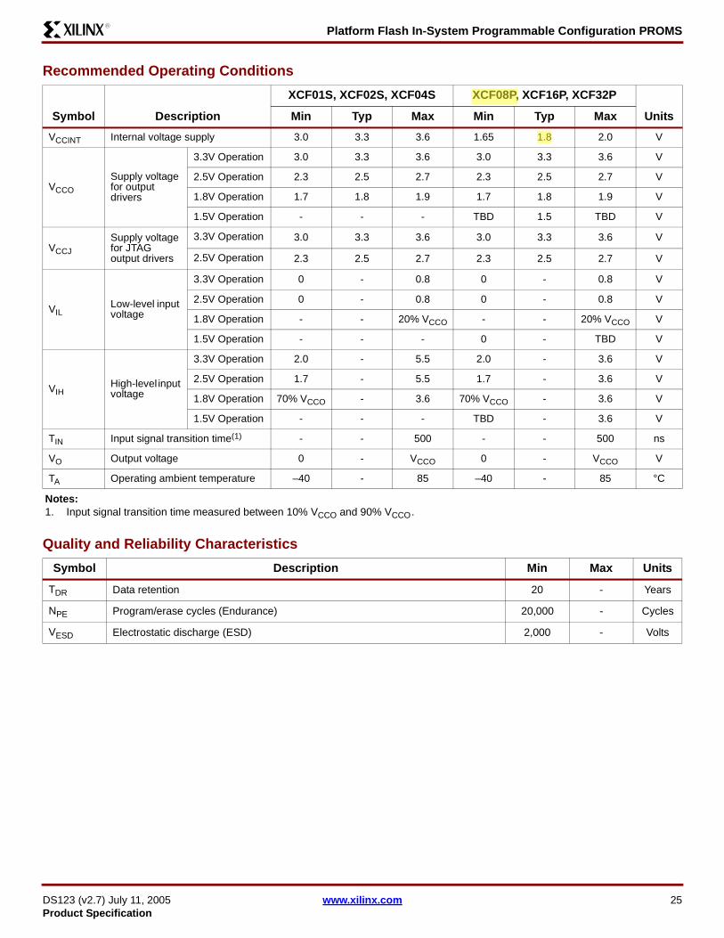
Platform Flash In-System Programmable Configuration PROMS
DS123 (v27) July 11 2005 wwwxilinxcom 26Product Specification
R
DC Characteristics Over Operating Conditions
Symbol Description
XCF01S XCF02S XCF04S
XCF08P XCF16P XCF32P
UnitsTest
Conditions Min MaxTest
Conditions Min Max
VOH
High-level output voltage for 33V outputs IOH = ndash4 mA 24 - IOH = ndash4 mA 24 - V
High-level output voltage for 25V outputs IOH = ndash500 microA VCCO ndash 04
- IOH = ndash500 microA VCCO ndash 04
- V
High-level output voltage for 18V outputs IOH = ndash50 microA VCCO ndash 04
- IOH = ndash50 microA VCCO ndash 04
- V
High-level output voltage for 15V outputs - - - IOH = TBD TBD - V
VOL
Low-level output voltage for 33V outputs IOL = 4 mA - 04 IOL = 4 mA - 04 V
Low-level output voltage for 25V outputs IOL = 500 microA - 04 IOL = 500 microA - 04 V
Low-level output voltage for 18V outputs IOL = 50 microA - 04 IOL = 50 microA - 04 V
Low-level output voltage for 15V outputs - - - IOL = TBD - TBD V
ICCINT Internal voltage supply current active mode 33 MHz - 10 33 MHz - 10 mA
ICCO(1)
Output driver supply current active serial mode 33 MHz - 10 33 MHz - 10 mA
Output driver supply current active parallel mode - - - 33 MHz - 40 mA
ICCJ JTAG supply current active mode Note (2) - 5 Note (2) - 5 mA
ICCINTS Internal voltage supply current standby mode Note (3) - 5 Note (3) - 5 mA
ICCOS Output driver supply current standby mode Note (3) - 1 Note (3) - 1 mA
ICCJS JTAG supply current standby mode Note (3) - 1 Note (3) - 1 mA
IILJ JTAG pins TMS TDI and TDO pull-up current VCCJ = maxVIN = GND - 100 VCCJ = max
VIN = GND - 100 microA
IIL Input leakage current
VCCINT = maxVCCO = maxVIN = GND or
VCCO
ndash10 10
VCCINT = maxVCCO = maxVIN = GND or
VCCO
ndash10 10 microA
IIH Input and output High-Z leakage current
VCCINT = maxVCCO = maxVIN = GND or
VCCO
ndash10 10
VCCINT = maxVCCO = maxVIN = GND or
VCCO
ndash10 10 microA
IILPSource current through internal pull-ups onEN_EXT_SEL REV_SEL0 REV_SEL1
- - -
VCCINT = maxVCCO = maxVIN = GND or
VCCO
- 100 microA
IIHP Sink current through internal pull-down on BUSY - - -
VCCINT = maxVCCO = maxVIN = GND or
VCCO
-100 - microA
huffman
XCF08P
Platform Flash In-System Programmable Configuration PROMS
DS123 (v27) July 11 2005 wwwxilinxcom 27Product Specification
R
CIN Input capacitance VIN = GNDf = 10 MHz - 8 VIN = GND
f = 10 MHz - 8 pF
COUT Output capacitance VIN = GNDf = 10 MHz - 14 VIN = GND
f = 10 MHz - 14 pF
Notes 1 Output driver supply current specification based on no load conditions2 TDITMSTCK non-static (active)3 CE High OE Low and TMSTDITCK static
Symbol Description
XCF01S XCF02S XCF04S
XCF08P XCF16P XCF32P
UnitsTest
Conditions Min MaxTest
Conditions Min Max
huffman
XCF08P
Platform Flash In-System Programmable Configuration PROMS
DS123 (v27) July 11 2005 wwwxilinxcom 28Product Specification
R
AC Characteristics Over Operating Conditions
Symbol Description
XCF01S XCF02S XCF04S
XCF08P XCF16P XCF32P
UnitsMin Max Min Max
TOEOERESET to data delay(6) when VCCO = 33V or 25V - 10 - 25 ns
OERESET to data delay(6) when VCCO = 18V - 30 - 25 ns
TCECE to data delay(5) when VCCO = 33V or 25V - 15 - 25 ns
CE to data delay(5) when VCCO = 18V - 30 - 25 ns
TCACCLK to data delay(7) when VCCO = 33V or 25V - 15 - 25 ns
CLK to data delay(7) when VCCO = 18V - 30 - 25 ns
TOH
Data hold from CE OERESET or CLKwhen VCCO = 33V or 25V 0 - 5 - ns
Data hold from CE OERESET or CLKwhen VCCO = 18V 0 - 5 - ns
TDF
CE or OERESET to data float delay(2)
when VCCO = 33V or 25V - 25 - 45 ns
CE or OERESET to data float delay(2)
when VCCO = 18V - 30 - 45 ns
TCYC
Clock period(7) (serial mode) when VCCO = 33V or 25V 30 - 25 - ns
Clock period(7) (serial mode) when VCCO = 18V 67 - 25 - ns
Clock period(7) (parallel mode) when VCCO = 33V or 25V - - 30 - ns
Clock period(7) (parallel mode) when VCCO = 18V - - 30 - ns
CE
OERESET
CLK
CLKOUT(optional)
BUSY(optional)
DATA
TCE
TLC THC
TSCE
TOE TCAC
THCE
THOE
TCYC
TOH
TDFTOH
THBTSBTOEC
TCEC
TCLKO
TCOH
TCDD
CF
EN_EXT_SEL
REV_SEL[10]
TSXT THXT
TSRV THRV
ds123_22_110403
huffman
XCF08P
Platform Flash In-System Programmable Configuration PROMS
DS123 (v27) July 11 2005 wwwxilinxcom 29Product Specification
R
TLCCLK Low time(3) when VCCO = 33V or 25V 10 - 12 - ns
CLK Low time(3) when VCCO = 18V 15 - 12 - ns
THCCLK High time(3) when VCCO = 33V or 25V 10 - 12 - ns
CLK High time(3) when VCCO = 18V 15 - 12 - ns
TSCE
CE setup time to CLK (guarantees proper counting)(3)
when VCCO = 33V or 25V 20 - 30 - ns
CE setup time to CLK (guarantees proper counting)(3)
when VCCO = 18V 30 30 - ns
THCE
CE hold time (guarantees counters are reset)(5)
when VCCO = 33V or 25V 250 - 2000 - ns
CE hold time (guarantees counters are reset)(5)
when VCCO = 18V 250 - 2000 - ns
THOE
OERESET hold time (guarantees counters are reset)(6)
when VCCO = 33V or 25V 250 - 2000 - ns
OERESET hold time (guarantees counters are reset)(6)
when VCCO = 18V 250 - 2000 - ns
TSBBUSY setup time to CLK when VCCO = 33V or 25V - - 12 - ns
BUSY setup time to CLK when VCCO = 18V - - 12 - ns
THBBUSY hold time to CLK when VCCO = 33V or 25V - - 8 - ns
BUSY hold time to CLK when VCCO = 18V - - 8 - ns
TCLKO
CLK input to CLKOUT output delay when VCCO = 33V or 25V - - - 35 ns
CLK input to CLKOUT output delay when VCCO = 18V - - - 35 ns
CLK input to CLKOUT output delay when VCCO = 33V or 25V with decompression(12) - - - 35 ns
CLK input to CLKOUT output delay when VCCO = 18V with decompression(12) - - - 35 ns
TCEC
CE to CLKOUT delay(8) with CLKOUT sourced from internal oscillator when VCCO = 33V or 25V - - 0 1 micros
CE to CLKOUT delay(8) with CLKOUT sourced from internal oscillator when VCCO = 18V - - 0 1 micros
CE to CLKOUT delay(8) with CLKOUT sourced from external CLK input when VCCO = 33V or 25V - - 0 2 CLK
cycles -
CE to CLKOUT delay(8) with CLKOUT sourced from external CLK input when VCCO = 18V - - 0 2 CLK
cycles -
TOEC
OERESET to CLKOUT delay(8) with CLKOUT sourced from internal oscillator when VCCO = 33V or 25V - - 0 1 micros
OERESET to CLKOUT delay(8) with CLKOUT sourced from internal oscillator when VCCO = 18V - - 0 1 micros
OERESET to CLKOUT delay(8) with CLKOUT sourced from external CLK input when VCCO = 33V or 25V 0 2 CLK
cycles -
OERESET to CLKOUT delay(8) with CLKOUT sourced from external CLK input when VCCO = 18V 0 2 CLK
cycles -
Symbol Description
XCF01S XCF02S XCF04S
XCF08P XCF16P XCF32P
UnitsMin Max Min Max
huffman
XCF08P
Platform Flash In-System Programmable Configuration PROMS
DS123 (v27) July 11 2005 wwwxilinxcom 30Product Specification
R
TCDDCLKOUT to data delay when VCCO = 33V or 25V(9) - - - 22 ns
CLKOUT to data delay when VCCO = 18V(9) - - - 22 ns
TDDC
Data setup time to CLKOUT when VCCO = 33V or 25V with decompression(9)(12) - - 5 ns
Data setup time to CLKOUT when VCCO = 18V with decompression(9)(12) - - 5 ns
TCOH
Data hold from CLKOUT when VCCO = 33V or 25V - - 3 - ns
Data hold from CLKOUT when VCCO = 18V - - 3 - ns
Data hold from CLKOUT when VCCO = 33V or 25V with decompression(12) - - 3 - ns
Data hold from CLKOUT when VCCO = 18V with decompression(12) - - 3 - ns
TSXT
EN_EXT_SEL setup time to CF (rising edge)when VCCO = 33V or 25V - - 300 - ns
EN_EXT_SEL setup time to CF (rising edge)when VCCO = 18V - - 300 - ns
THXT
EN_EXT_SEL hold time from CF (rising edge)when VCCO = 33V or 25V - - 300 - ns
EN_EXT_SEL hold time from CF (rising edge)when VCCO = 18V - - 300 - ns
TSRV
REV_SEL setup time to CF (rising edge)when VCCO = 33V or 25V - - 300 - ns
REV_SEL setup time to CF (rising edge)when VCCO = 18V - - 300 - ns
THRV
REV_SEL hold time from CF (rising edge)when VCCO = 33V or 25V - - 300 - ns
REV_SEL hold time from CF (rising edge)when VCCO = 18V - - 300 - ns
FF
CLKOUT default (fast) frequency(10) - - 25 50 MHz
CLKOUT default (fast) frequency with decompression(12) - - 125 25 MHz
Symbol Description
XCF01S XCF02S XCF04S
XCF08P XCF16P XCF32P
UnitsMin Max Min Max
huffman
XCF08P
Platform Flash In-System Programmable Configuration PROMS
DS123 (v27) July 11 2005 wwwxilinxcom 31Product Specification
R
FS
CLKOUT alternate (slower) frequency(11) - - 125 25 MHz
CLKOUT alternate (slower) frequency with decompression(12) - - 6 125 MHz
Notes 1 AC test load = 50 pF for XCF01SXCF02SXCF04S 30 pF for XCF08PXCF16PXCF32P2 Float delays are measured with 5 pF AC loads Transition is measured at plusmn200 mV from steady-state active levels3 Guaranteed by design not tested4 All AC parameters are measured with VIL = 00V and VIH = 30V5 If THCE High lt 2 micros TCE = 2 micros6 If THOE Low lt 2 micros TOE = 2 micros7 This is the minimum possible TCYC Actual TCYC = TCAC + FPGA Data setup time
Example With the XCF32P in serial mode with VCCO at 33V if FPGA Data setup time = 15 ns then the actual TCYC = 25 ns +15 ns = 40 ns8 The delay before the enabled CLKOUT signal begins clocking data out of the device is dependent on the clocking configuration The delay before
CLKOUT is enabled will increase if decompression is enabled 9 Slower CLK frequency option may be required to meet the FPGA data sheet setup time10 Typical CLKOUT default (fast) period = 25 ns (40 MHz)11 Typical CLKOUT alternate (slower) period = 50 ns (20 MHz)12 When decompression is enabled the CLKOUT signal becomes a controlled clock output When decompressed data is available CLKOUT will toggle
at frac12 the source clock frequency (either frac12 the selected internal clock frequency or frac12 the external CLK input frequency) When decompressed data is not available the CLKOUT pin is parked High If CLKOUT is used then it must be pulled High externally using a 47kΩ pull-up to VCCO
Symbol Description
XCF01S XCF02S XCF04S
XCF08P XCF16P XCF32P
UnitsMin Max Min Max
huffman
XCF08P
huffman
XCF08P
Platform Flash In-System Programmable Configuration PROMS
DS123 (v27) July 11 2005 wwwxilinxcom 32Product Specification
R
AC Characteristics Over Operating Conditions When Cascading
Symbol Description
XCF01S XCF02S XCF04S
XCF08P XCF16P XCF32P
UnitsMin Max Min Max
TCDF
CLK to output float delay(23) when VCCO = 25V or 33V - 25 - 20 ns
CLK to output float delay(23) when VCCO = 18V - 35 - 20 ns
TOCKCLK to CEO delay(35) when VCCO = 25V or 33V - 20 - 20 ns
CLK to CEO delay(35) when VCCO = 18V - 35 - 20 ns
TOCECE to CEO delay(36) when VCCO = 25V or 33V - 20 - 80 ns
CE to CEO delay(36) when VCCO = 18V - 35 - 80 ns
TOOEOERESET to CEO delay(3) when VCCO = 25V or 33V - 20 - 80 ns
OERESET to CEO delay(3) when VCCO = 18V - 35 - 80 ns
TCOCECLKOUT to CEO delay when VCCO = 25V or 33V - - - 20 ns
CLKOUT to CEO delay when VCCO = 18V - - - 20 ns
TCODF
CLKOUT to output float delay when VCCO = 25V or 33V - - - 25 ns
CLKOUT to output float delay when VCCO = 18V - - - 25 ns
Notes 1 AC test load = 50 pF for XCF01SXCF02SXCF04S 30 pF for XCF08PXCF16PXCF32P2 Float delays are measured with 5 pF AC loads Transition is measured at plusmn200 mV from steady state active levels3 Guaranteed by design not tested4 All AC parameters are measured with VIL = 00V and VIH = 30V5 For cascaded PROMs if the FPGArsquos dual-purpose configuration data pins are set to persist as configuration pins the minimum period is increased
based on the CLK to CEO and CE to data propagation delays- TCYC minimum = TOCK + TCE + FPGA Data setup time- TCAC maximum = TOCK + TCE
6 For cascaded PROMs if the FPGArsquos dual-purpose configuration data pins become general IO pins after configuration to allow for the disable to propagate to the cascaded PROMs and to avoid contention on the data lines following configuration the minimum period is increased based on the CE to CEO and CE to data propagation delays- TCYC minimum = TOCE + TCE - TCAC maximum = TOCK + TCE
OERESET
CE
CLK
CLKOUT(optional)
DATA
CEO
TOCETOOE
First BitLast Bit
TCDFTCODF
TOCK TCOCE
ds123_23_102203
huffman
XCF08P
huffman
XCF08P
Platform Flash In-System Programmable Configuration PROMS
DS123 (v27) July 11 2005 wwwxilinxcom 33Product Specification
R
Pinouts and Pin DescriptionsThe XCFxxS Platform Flash PROM is available in the VO20 and VOG20 packages The XCFxxP Platform Flash PROM isavailable in the VO48 VOG48 FS48 and FSG48 packages This section includes
bull Table 11 XCFxxS Pin Names and Descriptions page 33bull Figure 17 VO20VOG20 Pinout Diagram (Top View) with Pin Names page 34bull Table 12 XCFxxP Pin Names and Descriptions page 35bull Figure 18 VO48VOG48 Pinout Diagram (Top View) with Pin Names page 36bull Table 13 FS48FSG48 Pin NumberName Reference page 38bull Figure 19 FS48FSG48 Pinout Diagram (Top View) page 38
Notes 1 VO20VOG20 denotes a 20-pin (TSSOP) Plastic Thin Shrink Small Outline Package 2 VO48VOG48 denotes a 48-pin (TSOP) Plastic Thin Small Outline Package3 FS48FSG48 denotes a 48-pin (TFBGA) Plastic Thin Fine Pitch Ball Grid Array (08 mm pitch)
XCFxxS Pinouts and Pin DescriptionsTable 11 provides a list of the pin names and descriptions for the XCFxxS 20-pin VO20VOG20 package
Table 11 XCFxxS Pin Names and Descriptions
Pin NameBoundary
Scan OrderBoundary
Scan Function Pin Description20-pin TSSOP (VO20VOG20)
D04 Data Out D0 is the DATA output pin to provide data for configuring an
FPGA in serial mode The D0 output is set to a high-impedance state during ISPEN (when not clamped)
13 Output Enable
CLK 0 Data InConfiguration Clock Input Each rising edge on the CLK input increments the internal address counter if the CLK input is selected CE is Low and OERESET is High
3
OERESET
20 Data In Output EnableReset (Open-Drain IO) When Low this input holds the address counter reset and the DATA output is in a high-impedance state This is a bidirectional open-drain pin that is held Low while the PROM is reset Polarity is not programmable
819 Data Out
18 Output Enable
CE 15 Data InChip Enable Input When CE is High the device is put into low-power standby mode the address counter is reset and the DATA pins are put in a high-impedance state
10
CF22 Data Out Configuration Pulse (Open-Drain Output) Allows JTAG
CONFIG instruction to initiate FPGA configuration without powering down FPGA This is an open-drain output that is pulsed Low by the JTAG CONFIG command
721 Output Enable
CEO
12 Data OutChip Enable Output Chip Enable Output (CEO) is connected to the CE input of the next PROM in the chain This output is Low when CE is Low and OERESET input is High AND the internal address counter has been incremented beyond its Terminal Count (TC) value CEO returns to High when OERESET goes Low or CE goes High
13
11 Output Enable
TMS Mode Select
JTAG Mode Select Input The state of TMS on the rising edge of TCK determines the state transitions at the Test Access Port (TAP) controller TMS has an internal 50KΩ resistive pull-up to VCCJ to provide a logic 1 to the device if the pin is not driven
5
TCK ClockJTAG Clock Input This pin is the JTAG test clock It sequences the TAP controller and all the JTAG test and programming electronics
6
Platform Flash In-System Programmable Configuration PROMS
DS123 (v27) July 11 2005 wwwxilinxcom 34Product Specification
R
XCFxxS Pinout Diagram
TDI Data In
JTAG Serial Data Input This pin is the serial input to all JTAG instruction and data registers TDI has an internal 50KΩ resistive pull-up to VCCJ to provide a logic 1 to the device if the pin is not driven
4
TDO Data Out
JTAG Serial Data Output This pin is the serial output for all JTAG instruction and data registers TDO has an internal 50KΩ resistive pull-up to VCCJ to provide a logic 1 to the system if the pin is not driven
17
VCCINT +33V Supply Positive 33V supply voltage for internal logic 18
VCCO+33V 25V or 18V IO Supply Positive 33V 25V or 18V supply voltage connected to the output voltage drivers and input buffers
19
VCCJ+33V or 25V JTAG IO Supply Positive 33V 25V or 18V supply voltage connected to the TDO output voltage driver and TCK TMS and TDI input buffers
20
GND Ground 11
DNC Do not connect (These pins must be left unconnected) 2 9 12 14 15 16
Figure 17 VO20VOG20 Pinout Diagram (Top View) with Pin Names
Table 11 XCFxxS Pin Names and Descriptions (Continued)
Pin NameBoundary
Scan OrderBoundary
Scan Function Pin Description20-pin TSSOP (VO20VOG20)
VO20VOG20Top View
ds123_02_071304
1
2
3
4
5
6
7
8
9
10
20
19
18
17
16
15
14
13
12
11
D0
(DNC)
CLK
TDI
TMS
TCK
CF
OERESET
(DNC)
CE
VCCJ
VCCO
VCCINT
TDO
(DNC)
(DNC)
CEO
(DNC)
GND
(DNC)
Platform Flash In-System Programmable Configuration PROMS
DS123 (v27) July 11 2005 wwwxilinxcom 35Product Specification
R
XCFxxP Pinouts and Pin DescriptionsTable 12 provides a list of the pin names and descriptions for the XCFxxP 48-pin VO48VOG48 and 48-pin FS48FSG48packages
Table 12 XCFxxP Pin Names and Descriptions
Pin Name
Boundary Scan Order
Boundary Scan
Function Pin Description
48-pin TSOP (VO48VOG48)
48-pin TFBGA (FS48FSG48)
D028 Data Out
D0 is the DATA output pin to provide data for configuring an FPGA in serial mode D0-D7 are the DATA output pins to provide parallel data for configuring a Xilinx FPGA in SelectMap (parallel) mode The D0 output is set to a high-impedance state during ISPEN (when not clamped)The D1-D7 outputs are set to a high-impedance state during ISPEN (when not clamped) and when serial mode is selected for configuration The D1-D7 pins can be left unconnected when the PROM is used in serial mode
28 H627 Output Enable
D126 Data Out
29 H525 Output Enable
D224 Data Out
32 E523 Output Enable
D322 Data Out
33 D521 Output Enable
D420 Data Out
43 C519 Output Enable
D518 Data Out
44 B517 Output Enable
D616 Data Out
47 A515 Output Enable
D714 Data Out
48 A613 Output Enable
CLK 01 Data In
Configuration Clock Input An internal programmable control bit selects between the internal oscillator and the CLK input pin as the clock source to control the configuration sequence Each rising edge on the CLK input increments the internal address counter if the CLK input is selected CE is Low OERESET is High BUSY is Low (parallel mode only) and CF is High
12 B3
OERESET
04 Data In Output EnableReset (Open-Drain IO)When Low this input holds the address counter reset and the DATA and CLKOUT outputs are placed in a high-impedance state This is a bidirectional open-drain pin that is held Low while the PROM is reset Polarity is not programmable
11 A303 Data Out
02 Output Enable
CE 00 Data In
Chip Enable Input When CE is High the device is put into low-power standby mode the address counter is reset and the DATA and CLKOUT outputs are placed in a high-impedance state
13 B4
CF
11 Data InConfiguration Pulse (Open-Drain IO) As an output this pin allows the JTAG CONFIG instruction to initiate FPGA configuration without powering down the FPGA This is an open-drain signal that is pulsed Low by the JTAG CONFIG command As an input on the rising edge of CF the current design revision selection is sampled and the internal address counter is reset to the start address for the selected revision If unused the CF pin should be pulled High using an external 47KΩ pull-up to VCCO
6 D110 Data Out
09 Output Enable
Platform Flash In-System Programmable Configuration PROMS
DS123 (v27) July 11 2005 wwwxilinxcom 36Product Specification
R
CEO
06 Data OutChip Enable Output Chip Enable Output (CEO) is connected to the CE input of the next PROM in the chain This output is Low when CE is Low and OERESET input is High AND the internal address counter has been incremented beyond its Terminal Count (TC) value CEO returns to High when OERESET goes Low or CE goes High
10 D2
05 Output Enable
EN_EXT_SEL 31 Data In
Enable External Selection Input When this pin is Low design revision selection is controlled by the Revision Select pins When this pin is High design revision selection is controlled by the internal programmable Revision Select control bits EN_EXT_SEL has an internal 50KΩ resistive pull-up to VCCO to provide a logic 1 to the device if the pin is not driven
25 H4
REV_SEL0 30 Data InRevision Select[10] Inputs When the EN_EXT_SEL is Low the Revision Select pins are used to select the design revision to be enabled overriding the internal programmable Revision Select control bits The Revision Select[10] inputs have an internal 50KΩ resistive pull-up to VCCO to provide a logic 1 to the device if the pins are not driven
26 G3
REV_SEL1 29 Data In 27 G4
BUSY 12 Data In
Busy Input The BUSY input is enabled when parallel mode is selected for configuration When BUSY is High the internal address counter stops incrementing and the current data remains on the data pins On the first rising edge of CLK after BUSY transitions from High to Low the data for the next address is driven on the data pins When serial mode or decompression is enabled during device programming the BUSY input is disabled BUSY has an internal 50KΩ resistive pull-down to GND to provide a logic 0 to the device if the pin is not driven
5 C1
CLKOUT
08 Data Out
Configuration Clock Output An internal Programmable control bit enables the CLKOUT signal which is sourced from either the internal oscillator or the CLK input pin Each rising edge of the selected clock source increments the internal address counter if data is available CE is Low and OERESET is High Output data is available on the rising edge of CLKOUT CLKOUT is disabled if CE is High or OERESET is Low If decompression is enabled CLKOUT is parked High when decompressed data is not ready When CLKOUT is disabled the CLKOUT pin is put into a high-Z state If CLKOUT is used then it must be pulled High externally using a 47KΩ pull-up to VCCO
9 C2
07 Output Enable
TMS Mode Select
JTAG Mode Select Input The state of TMS on the rising edge of TCK determines the state transitions at the Test Access Port (TAP) controller TMS has an internal 50KΩ resistive pull-up to VCCJ to provide a logic 1 to the device if the pin is not driven
21 E2
TCK ClockJTAG Clock Input This pin is the JTAG test clock It sequences the TAP controller and all the JTAG test and programming electronics
20 H3
TDI Data In
JTAG Serial Data Input This pin is the serial input to all JTAG instruction and data registers TDI has an internal 50KΩ resistive pull-up to VCCJ to provide a logic 1 to the device if the pin is not driven
19 G1
Table 12 XCFxxP Pin Names and Descriptions (Continued)
Pin Name
Boundary Scan Order
Boundary Scan
Function Pin Description
48-pin TSOP (VO48VOG48)
48-pin TFBGA (FS48FSG48)
Platform Flash In-System Programmable Configuration PROMS
DS123 (v27) July 11 2005 wwwxilinxcom 37Product Specification
R
XCFxxP Pinout Diagrams
Figure 18 VO48VOG48 Pinout Diagram (Top View) with Pin Names
TDO Data Out
JTAG Serial Data Output This pin is the serial output for all JTAG instruction and data registers TDO has an internal 50KΩ resistive pull-up to VCCJ to provide a logic 1 to the system if the pin is not driven
22 E6
VCCINT +18V Supply Positive 18V supply voltage for internal logic 4 15 34
B1 E1 G6
VCCO+33V 25V or 18V IO Supply Positive 33V 25V or 18V supply voltage connected to the output voltage drivers and input buffers
8 30 38 45
B2 C6 D6 G5
VCCJ+33V or 25V JTAG IO Supply Positive 33V 25V or 18V supply voltage connected to the TDO output voltage driver and TCK TMS and TDI input buffers
24 H2
GND Ground2 7
17 23 31 36
46
A1 A2 B6 F1 F5 F6
H1
DNC Do Not Connect (These pins must be left unconnected)
1 3 14 16 18 35 37 39 40 41
42
A4 C3 C4 D3 D4 E3 E4 F2 F3 F4
G2
Table 12 XCFxxP Pin Names and Descriptions (Continued)
Pin Name
Boundary Scan Order
Boundary Scan
Function Pin Description
48-pin TSOP (VO48VOG48)
48-pin TFBGA (FS48FSG48)
123456789101112131415161718192021222324
484746454443424140393837363534333231302928272625
VO48VOG48Top View
DNCGNDDNC
VCCINTBUSY
CFGND
VCCOCLKOUT
CEOOERESET
CLKCE
DNCVCCINT
DNCGNDDNCTDI
TCKTMSTDOGND
D7D6GNDVCCOD5D4DNCDNCDNCDNCVCCODNCGNDDNCVCCINTD3D2GNDVCCOD1D0REV_SEL1REV_SEL0EN_EXT_SELVCCJ
Platform Flash In-System Programmable Configuration PROMS
DS123 (v27) July 11 2005 wwwxilinxcom 38Product Specification
R
Table 13 FS48FSG48 Pin NumberName ReferencePin
Number Pin NamePin
Number Pin NameA1 GND E1 VCCINT
A2 GND E2 TMS
A3 OERESET E3 DNC
A4 DNC E4 DNC
A5 D6 E5 D2
A6 D7 E6 TDO
B1 VCCINT F1 GND
B2 VCCO F2 DNC
B3 CLK F3 DNC
B4 CE F4 DNC
B5 D5 F5 GND
B6 GND F6 GND
C1 BUSY G1 TDI
C2 CLKOUT G2 DNC
C3 DNC G3 REV_SEL0
C4 DNC G4 REV_SEL1
C5 D4 G5 VCCO
C6 VCCO G6 VCCINT
D1 CF H1 GND
D2 CEO H2 VCCJ
D3 DNC H3 TCK
D4 DNC H4 EN_EXT_SEL
D5 D3 H5 D1
D6 VCCO H6 D0
Table 13 FS48FSG48 Pin NumberName ReferencePin
Number Pin NamePin
Number Pin Name
1 2 3 4 5 6
ds121_01_071604
A
B
C
D
E
F
G
H
FS48FSG48Top View
Platform Flash In-System Programmable Configuration PROMS
DS123 (v27) July 11 2005 wwwxilinxcom 39Product Specification
R
Ordering Information
Valid Ordering Combinations
Marking Information
XCF01SVO20 C XCF08PVO48 C XCF08PFS48 C XCF01SVOG20 C XCF08PVOG48 C XCF08PFSG48 C
XCF02SVO20 C XCF16PVO48 C XCF16PFS48 C XCF02SVOG20 C XCF16PVOG48 C XCF16PFSG48 C
XCF04SVO20 C XCF32PVO48 C XCF32PFS48 C XCF04SVOG20 C XCF32PVOG48 C XCF32PFSG48 C
XCF04S VO20 C
Operating RangeProcessingC = (TA = ndash40degC to +85degC)Package Type
VO20 = 20-pin TSSOP PackageVOG20 = 20-pin TSSOP Package Pb-free
Device NumberXCF01SXCF02SXCF04S
XCF32P FS48 C
Operating RangeProcessingC = (TA = ndash40degC to +85degC)Package Type
VO48 = 48-pin TSOP PackageVOG48 = 48-pin TSOP Package Pb-freeFS48 = 48-pin TFBGA PackageFSG48 = 48-pin TFBGA Package Pb-free
Device NumberXCF08PXCF16PXCF32P
XCF04S-V
Operating RangeProcessingC = (TA = ndash40degC to +85degC)Package Type
V = 20-pin TSSOP Package (VO20)VG = 20-pin TSSOP Package Pb-free (VOG20)VO48 = 48-pin TSOP Package (VO48)VOG48 = 48-pin TSOP Package Pb-free (VOG48)F48 = 48-pin TFBGA Package (FS48)FG48 = 48-pin TFBGA Package Pb-free (FSG48)
Device NumberXCF01SXCF02SXCF04SXCF08PXCF16PXCF32P
huffman
XCF08PFS48 C
huffman
XCF08P
huffman
XCF08P
Platform Flash In-System Programmable Configuration PROMS
DS123 (v27) July 11 2005 wwwxilinxcom 40Product Specification
R
Revision HistoryThe following table shows the revision history for this document
Date Version Revision
042903 10 Xilinx Initial Release
060303 11 Made edits to all pages
110503 20 Major revision
111803 21 Pinout corrections as followsbull Table 12
- For VO48 package removed 38 from VCCINT and added it to VCCO- For FS48 package removed pin D6 from VCCINT and added it to VCCO
bull Table 13 (FS48 package) - For pin D6 changed name from VCCINT to VCCO- For pin A4 changed name from GND to DNC
bull Figure 18 (VO48 package) For pin 38 changed name from VCCINT to VCCO
121503 22 bull Added specification (47kΩ) for recommended pull-up resistor on OERESET pin to section Reset and Power-On Reset Activation page 22
bull Added paragraph to section Standby Mode page 22 concerning use of a pull-up resistor andor buffer on the DONE pin
050704 23 bull Section Features page 1 Added package styles and 33 MHz configuration speed limit to itemized features
bull Section Description page 1 and following Added state conditions for CF and BUSY to the descriptive text
bull Table 2 page 3 Updated Virtex-II configuration bitstream sizesbull Section Design Revisioning page 9 Rewrittenbull Section PROM to FPGA Configuration Mode and Connections Summary
page 10 and following five instances Added instruction to tie CF High if it is not tied to the FPGArsquos PROG_B (PROGRAM) input
bull Figure 8 page 14 through Figure 15 page 21 Added footnote indicating the directionality of the CF pin in each configuration
bull Section IO Input Voltage Tolerance and Power Sequencing page 22 Rewrittenbull Table 10 page 23 Added CF column to truth table and added an additional row to
document the Low state of CFbull Section Absolute Maximum Ratings page 24 Revised VIN and VTS for rsquoPrsquo
devices bull Section Supply Voltage Requirements for Power-On Reset and Power-Down
page 24- Revised footnote callout number on TOER from Footnote (4) to Footnote (3)- Added Footnote (2) callout to TVCC
bull Section Recommended Operating Conditions page 25 - Added Typical (Typ) parameter columns and parameters for VCCINT and
VCCOVCCJ- Added 15V operation parameter row to VIL and VIH rsquoPrsquo devices- Revised VIH Min 25V operation from 20V to 17V- Added parameter row TIN and Max parameters
bull (Continued on next page)
Platform Flash In-System Programmable Configuration PROMS
DS123 (v27) July 11 2005 wwwxilinxcom 41Product Specification
R
050704(contrsquod)
23(contrsquod)
bull Section DC Characteristics Over Operating Conditions page 26 - Added parameter row and parameters for parallel configuration mode rsquoPrsquo
devices to ICCO- Added Footnote (1) and Footnote (2) with callouts in the Test Conditions column
for ICCJ ICCINTS ICCOS and ICCJS to define active and standby mode requirements
bull Section AC Characteristics Over Operating Conditions page 28 - Corrected description for second TCAC parameter line to show parameters for
18V VCCO- Revised Footnote (7) to indicate VCCO = 33V- Applied Footnote (7) to second TCYC parameter line
bull Section AC Characteristics Over Operating Conditions When Cascading page 32 Revised Footnote (5)TCYC Min and TCAC Min formulas
bull Table 12 page 35 - Added additional state conditions to CLK description- Added function of resetting the internal address counter to CF description
072004 24 bull Added Pb-free package options VOG20 FSG48 and VOG48bull Figure 8 page 14 and Figure 9 page 15 Corrected connection name for FPGA
DOUT (OPTIONAL Daisy-chained Slave FPGAs with different configurations) from DOUT to DIN
bull Section Absolute Maximum Ratings page 24 Removed parameter TSOL from table (TSOL information can be found in Package User Guide)
bull Table 2 page 3 Removed reference to XC2VP125 FPGA
101804 25 bull Table 1 page 1 Broke out VCCO VCCJ into two separate columnsbull Table 7 page 7 Added clarification of ID code die revision bitsbull Table 8 page 8 Deleted TCKMIN2 (bypass mode) and renamed TCKMIN1 to TCKMINbull Table Recommended Operating Conditions page 25 Separated VCCO and VCCJ
parametersbull Table DC Characteristics Over Operating Conditions page 26
- Added most parameter values for XCF08P XCF16P XCF32P devices- Added Footnote (1) to ICCO specifying no-load conditions
bull Table AC Characteristics Over Operating Conditions page 28 - Added most parameter values for XCF08P XCF16P XCF32P devices- Expanded Footnote (1) to include XCF08P XCF16P XCF32P devices- Added Footnote (8) through (11) relating to CLKOUT conditions for various
parameters- Added rows to TCYC specifying parameters for parallel mode- Added rows specifying parameters with decompression for TCLKO TCOH TFF
TSF- Added TDDC (setup time with decompression)
bull Table AC Characteristics Over Operating Conditions When Cascading page 32 - Added most parameter values for XCF08P XCF16P XCF32P devices- Separated Footnote (5) into Footnotes (5) and (6) to specify different
derivations of TCYC depending on whether dual-purpose configuration pins persist as configuration pins or become general IO pins after configuration
huffman
XCF08P
huffman
XCF08P
huffman
XCF08P
huffman
XCF08P
Platform Flash In-System Programmable Configuration PROMS
DS123 (v27) July 11 2005 wwwxilinxcom 42Product Specification
R
031405 26 bull Added Virtex-4 LXFXSX configuration data to Table 2 bull Corrected Virtex-II configuration data in Table 2bull Corrected Virtex-II Pro configuration data in Table 2bull Added Spartan-3L configuration data to Table 2bull Added Spartan-3E configuration data to Table 2bull Paragraph added to FPGA Master SelectMAP (Parallel) Mode (1) page 11bull Changes to DC Characteristics
- TOER changed page 26- IOL changed for VOL page 26- VCCO added to test conditions for IIL IILP IIHPand IIH page 26 Values modified
for IILP and IIHPbull Changes to AC Characteristics
- TLC and THC modified for 18V page 29- New rows added for TCEC and TOEC page 29
bull Minor changes to grammar and punctuationbull Add explanation of Preliminary to DC and AC Electrical Characteristics
071105 27 bull Move from Preliminary to Product Specificationbull Corrections to Virtex-4 configuration bitstream valuesbull Minor changes to figures 9 14 15 and 18bull Change to Internal Oscillator description page 8bull Change to CLKOUT description page 8
- Platform Flash In-System Programmable Configuration PROMS
-
- Features
- Description
- Programming
-
- In-System Programming
-
- OERESET
-
- External Programming
- Reliability and Endurance
-
- Design Security
-
- Read Protection
- Write Protection
-
- IEEE 11491 Boundary-Scan (JTAG)
-
- Instruction Register
-
- XCFxxS Instruction Register (8 bits wide)
- XCFxxP Instruction Register (16 bits wide)
-
- Boundary Scan Register
- Identification Registers
-
- IDCODE Register
- USERCODE Register
- Customer Code Register
-
- Platform Flash PROM TAP Characteristics
-
- TAP Timing
- TAP AC Parameters
-
- Additional Features for the XCFxxP
-
- Internal Oscillator
- CLKOUT
- Decompression
- Design Revisioning
-
- PROM to FPGA Configuration Mode and Connections Summary
-
- FPGA Master Serial Mode
- FPGA Slave Serial Mode
- Serial Daisy Chain
- FPGA Master SelectMAP (Parallel) Mode
- FPGA Slave SelectMAP (Parallel) Mode
- FPGA SelectMAP (Parallel) Device Chaining
- Cascading Configuration PROMs
- Initiating FPGA Configuration
-
- Configuration PROM to FPGA Device Interface Connection Diagrams
- Reset and Power-On Reset Activation
- IO Input Voltage Tolerance and Power Sequencing
- Standby Mode
- DC Electrical Characteristics
- AC Electrical Characteristics
-
- Absolute Maximum Ratings
- Supply Voltage Requirements for Power-On Reset and Power-Down
- Recommended Operating Conditions
- Quality and Reliability Characteristics
- DC Characteristics Over Operating Conditions
- AC Characteristics Over Operating Conditions
- AC Characteristics Over Operating Conditions When Cascading
-
- Pinouts and Pin Descriptions
-
- XCFxxS Pinouts and Pin Descriptions
- XCFxxS Pinout Diagram
- XCFxxP Pinouts and Pin Descriptions
- XCFxxP Pinout Diagrams
-
- Ordering Information
- Valid Ordering Combinations
- Marking Information
- Revision History
-
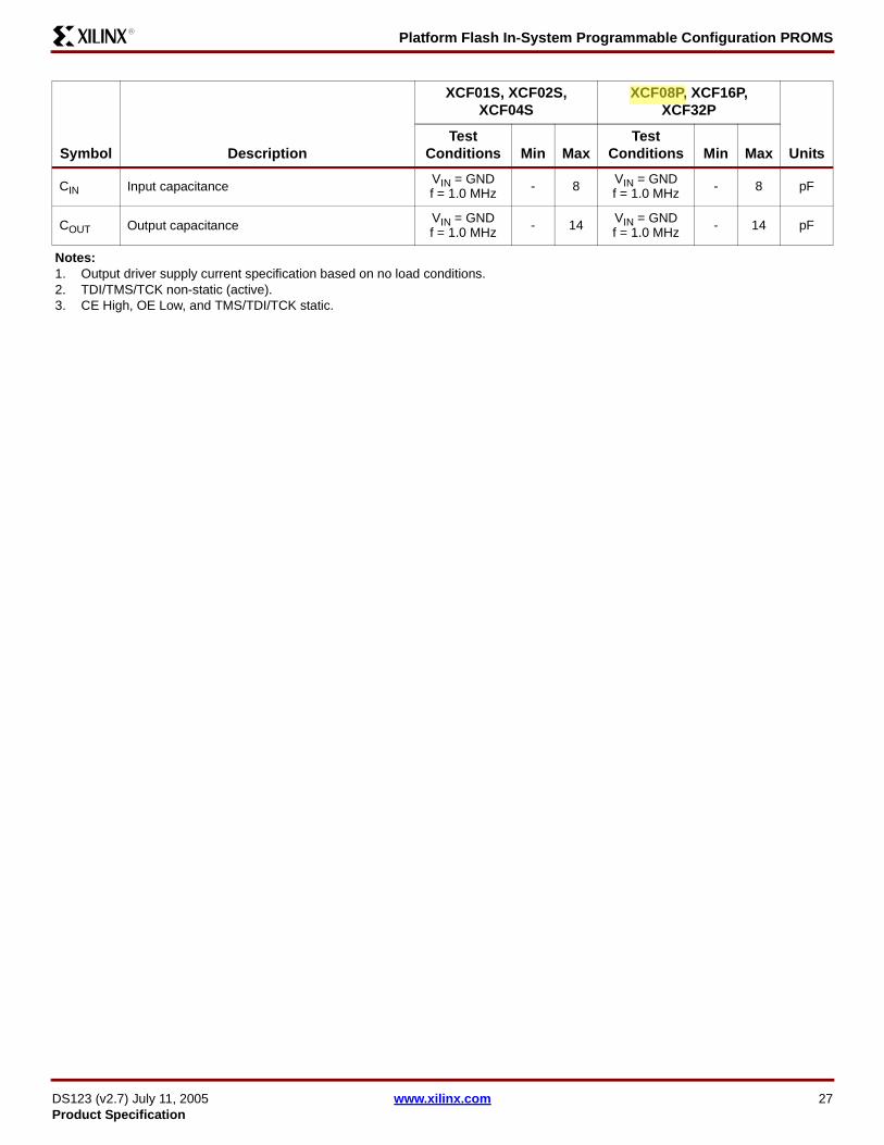
Platform Flash In-System Programmable Configuration PROMS
DS123 (v27) July 11 2005 wwwxilinxcom 29Product Specification
R
TLCCLK Low time(3) when VCCO = 33V or 25V 10 - 12 - ns
CLK Low time(3) when VCCO = 18V 15 - 12 - ns
THCCLK High time(3) when VCCO = 33V or 25V 10 - 12 - ns
CLK High time(3) when VCCO = 18V 15 - 12 - ns
TSCE
CE setup time to CLK (guarantees proper counting)(3)
when VCCO = 33V or 25V 20 - 30 - ns
CE setup time to CLK (guarantees proper counting)(3)
when VCCO = 18V 30 30 - ns
THCE
CE hold time (guarantees counters are reset)(5)
when VCCO = 33V or 25V 250 - 2000 - ns
CE hold time (guarantees counters are reset)(5)
when VCCO = 18V 250 - 2000 - ns
THOE
OERESET hold time (guarantees counters are reset)(6)
when VCCO = 33V or 25V 250 - 2000 - ns
OERESET hold time (guarantees counters are reset)(6)
when VCCO = 18V 250 - 2000 - ns
TSBBUSY setup time to CLK when VCCO = 33V or 25V - - 12 - ns
BUSY setup time to CLK when VCCO = 18V - - 12 - ns
THBBUSY hold time to CLK when VCCO = 33V or 25V - - 8 - ns
BUSY hold time to CLK when VCCO = 18V - - 8 - ns
TCLKO
CLK input to CLKOUT output delay when VCCO = 33V or 25V - - - 35 ns
CLK input to CLKOUT output delay when VCCO = 18V - - - 35 ns
CLK input to CLKOUT output delay when VCCO = 33V or 25V with decompression(12) - - - 35 ns
CLK input to CLKOUT output delay when VCCO = 18V with decompression(12) - - - 35 ns
TCEC
CE to CLKOUT delay(8) with CLKOUT sourced from internal oscillator when VCCO = 33V or 25V - - 0 1 micros
CE to CLKOUT delay(8) with CLKOUT sourced from internal oscillator when VCCO = 18V - - 0 1 micros
CE to CLKOUT delay(8) with CLKOUT sourced from external CLK input when VCCO = 33V or 25V - - 0 2 CLK
cycles -
CE to CLKOUT delay(8) with CLKOUT sourced from external CLK input when VCCO = 18V - - 0 2 CLK
cycles -
TOEC
OERESET to CLKOUT delay(8) with CLKOUT sourced from internal oscillator when VCCO = 33V or 25V - - 0 1 micros
OERESET to CLKOUT delay(8) with CLKOUT sourced from internal oscillator when VCCO = 18V - - 0 1 micros
OERESET to CLKOUT delay(8) with CLKOUT sourced from external CLK input when VCCO = 33V or 25V 0 2 CLK
cycles -
OERESET to CLKOUT delay(8) with CLKOUT sourced from external CLK input when VCCO = 18V 0 2 CLK
cycles -
Symbol Description
XCF01S XCF02S XCF04S
XCF08P XCF16P XCF32P
UnitsMin Max Min Max
huffman
XCF08P
Platform Flash In-System Programmable Configuration PROMS
DS123 (v27) July 11 2005 wwwxilinxcom 30Product Specification
R
TCDDCLKOUT to data delay when VCCO = 33V or 25V(9) - - - 22 ns
CLKOUT to data delay when VCCO = 18V(9) - - - 22 ns
TDDC
Data setup time to CLKOUT when VCCO = 33V or 25V with decompression(9)(12) - - 5 ns
Data setup time to CLKOUT when VCCO = 18V with decompression(9)(12) - - 5 ns
TCOH
Data hold from CLKOUT when VCCO = 33V or 25V - - 3 - ns
Data hold from CLKOUT when VCCO = 18V - - 3 - ns
Data hold from CLKOUT when VCCO = 33V or 25V with decompression(12) - - 3 - ns
Data hold from CLKOUT when VCCO = 18V with decompression(12) - - 3 - ns
TSXT
EN_EXT_SEL setup time to CF (rising edge)when VCCO = 33V or 25V - - 300 - ns
EN_EXT_SEL setup time to CF (rising edge)when VCCO = 18V - - 300 - ns
THXT
EN_EXT_SEL hold time from CF (rising edge)when VCCO = 33V or 25V - - 300 - ns
EN_EXT_SEL hold time from CF (rising edge)when VCCO = 18V - - 300 - ns
TSRV
REV_SEL setup time to CF (rising edge)when VCCO = 33V or 25V - - 300 - ns
REV_SEL setup time to CF (rising edge)when VCCO = 18V - - 300 - ns
THRV
REV_SEL hold time from CF (rising edge)when VCCO = 33V or 25V - - 300 - ns
REV_SEL hold time from CF (rising edge)when VCCO = 18V - - 300 - ns
FF
CLKOUT default (fast) frequency(10) - - 25 50 MHz
CLKOUT default (fast) frequency with decompression(12) - - 125 25 MHz
Symbol Description
XCF01S XCF02S XCF04S
XCF08P XCF16P XCF32P
UnitsMin Max Min Max
huffman
XCF08P
Platform Flash In-System Programmable Configuration PROMS
DS123 (v27) July 11 2005 wwwxilinxcom 31Product Specification
R
FS
CLKOUT alternate (slower) frequency(11) - - 125 25 MHz
CLKOUT alternate (slower) frequency with decompression(12) - - 6 125 MHz
Notes 1 AC test load = 50 pF for XCF01SXCF02SXCF04S 30 pF for XCF08PXCF16PXCF32P2 Float delays are measured with 5 pF AC loads Transition is measured at plusmn200 mV from steady-state active levels3 Guaranteed by design not tested4 All AC parameters are measured with VIL = 00V and VIH = 30V5 If THCE High lt 2 micros TCE = 2 micros6 If THOE Low lt 2 micros TOE = 2 micros7 This is the minimum possible TCYC Actual TCYC = TCAC + FPGA Data setup time
Example With the XCF32P in serial mode with VCCO at 33V if FPGA Data setup time = 15 ns then the actual TCYC = 25 ns +15 ns = 40 ns8 The delay before the enabled CLKOUT signal begins clocking data out of the device is dependent on the clocking configuration The delay before
CLKOUT is enabled will increase if decompression is enabled 9 Slower CLK frequency option may be required to meet the FPGA data sheet setup time10 Typical CLKOUT default (fast) period = 25 ns (40 MHz)11 Typical CLKOUT alternate (slower) period = 50 ns (20 MHz)12 When decompression is enabled the CLKOUT signal becomes a controlled clock output When decompressed data is available CLKOUT will toggle
at frac12 the source clock frequency (either frac12 the selected internal clock frequency or frac12 the external CLK input frequency) When decompressed data is not available the CLKOUT pin is parked High If CLKOUT is used then it must be pulled High externally using a 47kΩ pull-up to VCCO
Symbol Description
XCF01S XCF02S XCF04S
XCF08P XCF16P XCF32P
UnitsMin Max Min Max
huffman
XCF08P
huffman
XCF08P
Platform Flash In-System Programmable Configuration PROMS
DS123 (v27) July 11 2005 wwwxilinxcom 32Product Specification
R
AC Characteristics Over Operating Conditions When Cascading
Symbol Description
XCF01S XCF02S XCF04S
XCF08P XCF16P XCF32P
UnitsMin Max Min Max
TCDF
CLK to output float delay(23) when VCCO = 25V or 33V - 25 - 20 ns
CLK to output float delay(23) when VCCO = 18V - 35 - 20 ns
TOCKCLK to CEO delay(35) when VCCO = 25V or 33V - 20 - 20 ns
CLK to CEO delay(35) when VCCO = 18V - 35 - 20 ns
TOCECE to CEO delay(36) when VCCO = 25V or 33V - 20 - 80 ns
CE to CEO delay(36) when VCCO = 18V - 35 - 80 ns
TOOEOERESET to CEO delay(3) when VCCO = 25V or 33V - 20 - 80 ns
OERESET to CEO delay(3) when VCCO = 18V - 35 - 80 ns
TCOCECLKOUT to CEO delay when VCCO = 25V or 33V - - - 20 ns
CLKOUT to CEO delay when VCCO = 18V - - - 20 ns
TCODF
CLKOUT to output float delay when VCCO = 25V or 33V - - - 25 ns
CLKOUT to output float delay when VCCO = 18V - - - 25 ns
Notes 1 AC test load = 50 pF for XCF01SXCF02SXCF04S 30 pF for XCF08PXCF16PXCF32P2 Float delays are measured with 5 pF AC loads Transition is measured at plusmn200 mV from steady state active levels3 Guaranteed by design not tested4 All AC parameters are measured with VIL = 00V and VIH = 30V5 For cascaded PROMs if the FPGArsquos dual-purpose configuration data pins are set to persist as configuration pins the minimum period is increased
based on the CLK to CEO and CE to data propagation delays- TCYC minimum = TOCK + TCE + FPGA Data setup time- TCAC maximum = TOCK + TCE
6 For cascaded PROMs if the FPGArsquos dual-purpose configuration data pins become general IO pins after configuration to allow for the disable to propagate to the cascaded PROMs and to avoid contention on the data lines following configuration the minimum period is increased based on the CE to CEO and CE to data propagation delays- TCYC minimum = TOCE + TCE - TCAC maximum = TOCK + TCE
OERESET
CE
CLK
CLKOUT(optional)
DATA
CEO
TOCETOOE
First BitLast Bit
TCDFTCODF
TOCK TCOCE
ds123_23_102203
huffman
XCF08P
huffman
XCF08P
Platform Flash In-System Programmable Configuration PROMS
DS123 (v27) July 11 2005 wwwxilinxcom 33Product Specification
R
Pinouts and Pin DescriptionsThe XCFxxS Platform Flash PROM is available in the VO20 and VOG20 packages The XCFxxP Platform Flash PROM isavailable in the VO48 VOG48 FS48 and FSG48 packages This section includes
bull Table 11 XCFxxS Pin Names and Descriptions page 33bull Figure 17 VO20VOG20 Pinout Diagram (Top View) with Pin Names page 34bull Table 12 XCFxxP Pin Names and Descriptions page 35bull Figure 18 VO48VOG48 Pinout Diagram (Top View) with Pin Names page 36bull Table 13 FS48FSG48 Pin NumberName Reference page 38bull Figure 19 FS48FSG48 Pinout Diagram (Top View) page 38
Notes 1 VO20VOG20 denotes a 20-pin (TSSOP) Plastic Thin Shrink Small Outline Package 2 VO48VOG48 denotes a 48-pin (TSOP) Plastic Thin Small Outline Package3 FS48FSG48 denotes a 48-pin (TFBGA) Plastic Thin Fine Pitch Ball Grid Array (08 mm pitch)
XCFxxS Pinouts and Pin DescriptionsTable 11 provides a list of the pin names and descriptions for the XCFxxS 20-pin VO20VOG20 package
Table 11 XCFxxS Pin Names and Descriptions
Pin NameBoundary
Scan OrderBoundary
Scan Function Pin Description20-pin TSSOP (VO20VOG20)
D04 Data Out D0 is the DATA output pin to provide data for configuring an
FPGA in serial mode The D0 output is set to a high-impedance state during ISPEN (when not clamped)
13 Output Enable
CLK 0 Data InConfiguration Clock Input Each rising edge on the CLK input increments the internal address counter if the CLK input is selected CE is Low and OERESET is High
3
OERESET
20 Data In Output EnableReset (Open-Drain IO) When Low this input holds the address counter reset and the DATA output is in a high-impedance state This is a bidirectional open-drain pin that is held Low while the PROM is reset Polarity is not programmable
819 Data Out
18 Output Enable
CE 15 Data InChip Enable Input When CE is High the device is put into low-power standby mode the address counter is reset and the DATA pins are put in a high-impedance state
10
CF22 Data Out Configuration Pulse (Open-Drain Output) Allows JTAG
CONFIG instruction to initiate FPGA configuration without powering down FPGA This is an open-drain output that is pulsed Low by the JTAG CONFIG command
721 Output Enable
CEO
12 Data OutChip Enable Output Chip Enable Output (CEO) is connected to the CE input of the next PROM in the chain This output is Low when CE is Low and OERESET input is High AND the internal address counter has been incremented beyond its Terminal Count (TC) value CEO returns to High when OERESET goes Low or CE goes High
13
11 Output Enable
TMS Mode Select
JTAG Mode Select Input The state of TMS on the rising edge of TCK determines the state transitions at the Test Access Port (TAP) controller TMS has an internal 50KΩ resistive pull-up to VCCJ to provide a logic 1 to the device if the pin is not driven
5
TCK ClockJTAG Clock Input This pin is the JTAG test clock It sequences the TAP controller and all the JTAG test and programming electronics
6
Platform Flash In-System Programmable Configuration PROMS
DS123 (v27) July 11 2005 wwwxilinxcom 34Product Specification
R
XCFxxS Pinout Diagram
TDI Data In
JTAG Serial Data Input This pin is the serial input to all JTAG instruction and data registers TDI has an internal 50KΩ resistive pull-up to VCCJ to provide a logic 1 to the device if the pin is not driven
4
TDO Data Out
JTAG Serial Data Output This pin is the serial output for all JTAG instruction and data registers TDO has an internal 50KΩ resistive pull-up to VCCJ to provide a logic 1 to the system if the pin is not driven
17
VCCINT +33V Supply Positive 33V supply voltage for internal logic 18
VCCO+33V 25V or 18V IO Supply Positive 33V 25V or 18V supply voltage connected to the output voltage drivers and input buffers
19
VCCJ+33V or 25V JTAG IO Supply Positive 33V 25V or 18V supply voltage connected to the TDO output voltage driver and TCK TMS and TDI input buffers
20
GND Ground 11
DNC Do not connect (These pins must be left unconnected) 2 9 12 14 15 16
Figure 17 VO20VOG20 Pinout Diagram (Top View) with Pin Names
Table 11 XCFxxS Pin Names and Descriptions (Continued)
Pin NameBoundary
Scan OrderBoundary
Scan Function Pin Description20-pin TSSOP (VO20VOG20)
VO20VOG20Top View
ds123_02_071304
1
2
3
4
5
6
7
8
9
10
20
19
18
17
16
15
14
13
12
11
D0
(DNC)
CLK
TDI
TMS
TCK
CF
OERESET
(DNC)
CE
VCCJ
VCCO
VCCINT
TDO
(DNC)
(DNC)
CEO
(DNC)
GND
(DNC)
Platform Flash In-System Programmable Configuration PROMS
DS123 (v27) July 11 2005 wwwxilinxcom 35Product Specification
R
XCFxxP Pinouts and Pin DescriptionsTable 12 provides a list of the pin names and descriptions for the XCFxxP 48-pin VO48VOG48 and 48-pin FS48FSG48packages
Table 12 XCFxxP Pin Names and Descriptions
Pin Name
Boundary Scan Order
Boundary Scan
Function Pin Description
48-pin TSOP (VO48VOG48)
48-pin TFBGA (FS48FSG48)
D028 Data Out
D0 is the DATA output pin to provide data for configuring an FPGA in serial mode D0-D7 are the DATA output pins to provide parallel data for configuring a Xilinx FPGA in SelectMap (parallel) mode The D0 output is set to a high-impedance state during ISPEN (when not clamped)The D1-D7 outputs are set to a high-impedance state during ISPEN (when not clamped) and when serial mode is selected for configuration The D1-D7 pins can be left unconnected when the PROM is used in serial mode
28 H627 Output Enable
D126 Data Out
29 H525 Output Enable
D224 Data Out
32 E523 Output Enable
D322 Data Out
33 D521 Output Enable
D420 Data Out
43 C519 Output Enable
D518 Data Out
44 B517 Output Enable
D616 Data Out
47 A515 Output Enable
D714 Data Out
48 A613 Output Enable
CLK 01 Data In
Configuration Clock Input An internal programmable control bit selects between the internal oscillator and the CLK input pin as the clock source to control the configuration sequence Each rising edge on the CLK input increments the internal address counter if the CLK input is selected CE is Low OERESET is High BUSY is Low (parallel mode only) and CF is High
12 B3
OERESET
04 Data In Output EnableReset (Open-Drain IO)When Low this input holds the address counter reset and the DATA and CLKOUT outputs are placed in a high-impedance state This is a bidirectional open-drain pin that is held Low while the PROM is reset Polarity is not programmable
11 A303 Data Out
02 Output Enable
CE 00 Data In
Chip Enable Input When CE is High the device is put into low-power standby mode the address counter is reset and the DATA and CLKOUT outputs are placed in a high-impedance state
13 B4
CF
11 Data InConfiguration Pulse (Open-Drain IO) As an output this pin allows the JTAG CONFIG instruction to initiate FPGA configuration without powering down the FPGA This is an open-drain signal that is pulsed Low by the JTAG CONFIG command As an input on the rising edge of CF the current design revision selection is sampled and the internal address counter is reset to the start address for the selected revision If unused the CF pin should be pulled High using an external 47KΩ pull-up to VCCO
6 D110 Data Out
09 Output Enable
Platform Flash In-System Programmable Configuration PROMS
DS123 (v27) July 11 2005 wwwxilinxcom 36Product Specification
R
CEO
06 Data OutChip Enable Output Chip Enable Output (CEO) is connected to the CE input of the next PROM in the chain This output is Low when CE is Low and OERESET input is High AND the internal address counter has been incremented beyond its Terminal Count (TC) value CEO returns to High when OERESET goes Low or CE goes High
10 D2
05 Output Enable
EN_EXT_SEL 31 Data In
Enable External Selection Input When this pin is Low design revision selection is controlled by the Revision Select pins When this pin is High design revision selection is controlled by the internal programmable Revision Select control bits EN_EXT_SEL has an internal 50KΩ resistive pull-up to VCCO to provide a logic 1 to the device if the pin is not driven
25 H4
REV_SEL0 30 Data InRevision Select[10] Inputs When the EN_EXT_SEL is Low the Revision Select pins are used to select the design revision to be enabled overriding the internal programmable Revision Select control bits The Revision Select[10] inputs have an internal 50KΩ resistive pull-up to VCCO to provide a logic 1 to the device if the pins are not driven
26 G3
REV_SEL1 29 Data In 27 G4
BUSY 12 Data In
Busy Input The BUSY input is enabled when parallel mode is selected for configuration When BUSY is High the internal address counter stops incrementing and the current data remains on the data pins On the first rising edge of CLK after BUSY transitions from High to Low the data for the next address is driven on the data pins When serial mode or decompression is enabled during device programming the BUSY input is disabled BUSY has an internal 50KΩ resistive pull-down to GND to provide a logic 0 to the device if the pin is not driven
5 C1
CLKOUT
08 Data Out
Configuration Clock Output An internal Programmable control bit enables the CLKOUT signal which is sourced from either the internal oscillator or the CLK input pin Each rising edge of the selected clock source increments the internal address counter if data is available CE is Low and OERESET is High Output data is available on the rising edge of CLKOUT CLKOUT is disabled if CE is High or OERESET is Low If decompression is enabled CLKOUT is parked High when decompressed data is not ready When CLKOUT is disabled the CLKOUT pin is put into a high-Z state If CLKOUT is used then it must be pulled High externally using a 47KΩ pull-up to VCCO
9 C2
07 Output Enable
TMS Mode Select
JTAG Mode Select Input The state of TMS on the rising edge of TCK determines the state transitions at the Test Access Port (TAP) controller TMS has an internal 50KΩ resistive pull-up to VCCJ to provide a logic 1 to the device if the pin is not driven
21 E2
TCK ClockJTAG Clock Input This pin is the JTAG test clock It sequences the TAP controller and all the JTAG test and programming electronics
20 H3
TDI Data In
JTAG Serial Data Input This pin is the serial input to all JTAG instruction and data registers TDI has an internal 50KΩ resistive pull-up to VCCJ to provide a logic 1 to the device if the pin is not driven
19 G1
Table 12 XCFxxP Pin Names and Descriptions (Continued)
Pin Name
Boundary Scan Order
Boundary Scan
Function Pin Description
48-pin TSOP (VO48VOG48)
48-pin TFBGA (FS48FSG48)
Platform Flash In-System Programmable Configuration PROMS
DS123 (v27) July 11 2005 wwwxilinxcom 37Product Specification
R
XCFxxP Pinout Diagrams
Figure 18 VO48VOG48 Pinout Diagram (Top View) with Pin Names
TDO Data Out
JTAG Serial Data Output This pin is the serial output for all JTAG instruction and data registers TDO has an internal 50KΩ resistive pull-up to VCCJ to provide a logic 1 to the system if the pin is not driven
22 E6
VCCINT +18V Supply Positive 18V supply voltage for internal logic 4 15 34
B1 E1 G6
VCCO+33V 25V or 18V IO Supply Positive 33V 25V or 18V supply voltage connected to the output voltage drivers and input buffers
8 30 38 45
B2 C6 D6 G5
VCCJ+33V or 25V JTAG IO Supply Positive 33V 25V or 18V supply voltage connected to the TDO output voltage driver and TCK TMS and TDI input buffers
24 H2
GND Ground2 7
17 23 31 36
46
A1 A2 B6 F1 F5 F6
H1
DNC Do Not Connect (These pins must be left unconnected)
1 3 14 16 18 35 37 39 40 41
42
A4 C3 C4 D3 D4 E3 E4 F2 F3 F4
G2
Table 12 XCFxxP Pin Names and Descriptions (Continued)
Pin Name
Boundary Scan Order
Boundary Scan
Function Pin Description
48-pin TSOP (VO48VOG48)
48-pin TFBGA (FS48FSG48)
123456789101112131415161718192021222324
484746454443424140393837363534333231302928272625
VO48VOG48Top View
DNCGNDDNC
VCCINTBUSY
CFGND
VCCOCLKOUT
CEOOERESET
CLKCE
DNCVCCINT
DNCGNDDNCTDI
TCKTMSTDOGND
D7D6GNDVCCOD5D4DNCDNCDNCDNCVCCODNCGNDDNCVCCINTD3D2GNDVCCOD1D0REV_SEL1REV_SEL0EN_EXT_SELVCCJ
Platform Flash In-System Programmable Configuration PROMS
DS123 (v27) July 11 2005 wwwxilinxcom 38Product Specification
R
Table 13 FS48FSG48 Pin NumberName ReferencePin
Number Pin NamePin
Number Pin NameA1 GND E1 VCCINT
A2 GND E2 TMS
A3 OERESET E3 DNC
A4 DNC E4 DNC
A5 D6 E5 D2
A6 D7 E6 TDO
B1 VCCINT F1 GND
B2 VCCO F2 DNC
B3 CLK F3 DNC
B4 CE F4 DNC
B5 D5 F5 GND
B6 GND F6 GND
C1 BUSY G1 TDI
C2 CLKOUT G2 DNC
C3 DNC G3 REV_SEL0
C4 DNC G4 REV_SEL1
C5 D4 G5 VCCO
C6 VCCO G6 VCCINT
D1 CF H1 GND
D2 CEO H2 VCCJ
D3 DNC H3 TCK
D4 DNC H4 EN_EXT_SEL
D5 D3 H5 D1
D6 VCCO H6 D0
Table 13 FS48FSG48 Pin NumberName ReferencePin
Number Pin NamePin
Number Pin Name
1 2 3 4 5 6
ds121_01_071604
A
B
C
D
E
F
G
H
FS48FSG48Top View
Platform Flash In-System Programmable Configuration PROMS
DS123 (v27) July 11 2005 wwwxilinxcom 39Product Specification
R
Ordering Information
Valid Ordering Combinations
Marking Information
XCF01SVO20 C XCF08PVO48 C XCF08PFS48 C XCF01SVOG20 C XCF08PVOG48 C XCF08PFSG48 C
XCF02SVO20 C XCF16PVO48 C XCF16PFS48 C XCF02SVOG20 C XCF16PVOG48 C XCF16PFSG48 C
XCF04SVO20 C XCF32PVO48 C XCF32PFS48 C XCF04SVOG20 C XCF32PVOG48 C XCF32PFSG48 C
XCF04S VO20 C
Operating RangeProcessingC = (TA = ndash40degC to +85degC)Package Type
VO20 = 20-pin TSSOP PackageVOG20 = 20-pin TSSOP Package Pb-free
Device NumberXCF01SXCF02SXCF04S
XCF32P FS48 C
Operating RangeProcessingC = (TA = ndash40degC to +85degC)Package Type
VO48 = 48-pin TSOP PackageVOG48 = 48-pin TSOP Package Pb-freeFS48 = 48-pin TFBGA PackageFSG48 = 48-pin TFBGA Package Pb-free
Device NumberXCF08PXCF16PXCF32P
XCF04S-V
Operating RangeProcessingC = (TA = ndash40degC to +85degC)Package Type
V = 20-pin TSSOP Package (VO20)VG = 20-pin TSSOP Package Pb-free (VOG20)VO48 = 48-pin TSOP Package (VO48)VOG48 = 48-pin TSOP Package Pb-free (VOG48)F48 = 48-pin TFBGA Package (FS48)FG48 = 48-pin TFBGA Package Pb-free (FSG48)
Device NumberXCF01SXCF02SXCF04SXCF08PXCF16PXCF32P
huffman
XCF08PFS48 C
huffman
XCF08P
huffman
XCF08P
Platform Flash In-System Programmable Configuration PROMS
DS123 (v27) July 11 2005 wwwxilinxcom 40Product Specification
R
Revision HistoryThe following table shows the revision history for this document
Date Version Revision
042903 10 Xilinx Initial Release
060303 11 Made edits to all pages
110503 20 Major revision
111803 21 Pinout corrections as followsbull Table 12
- For VO48 package removed 38 from VCCINT and added it to VCCO- For FS48 package removed pin D6 from VCCINT and added it to VCCO
bull Table 13 (FS48 package) - For pin D6 changed name from VCCINT to VCCO- For pin A4 changed name from GND to DNC
bull Figure 18 (VO48 package) For pin 38 changed name from VCCINT to VCCO
121503 22 bull Added specification (47kΩ) for recommended pull-up resistor on OERESET pin to section Reset and Power-On Reset Activation page 22
bull Added paragraph to section Standby Mode page 22 concerning use of a pull-up resistor andor buffer on the DONE pin
050704 23 bull Section Features page 1 Added package styles and 33 MHz configuration speed limit to itemized features
bull Section Description page 1 and following Added state conditions for CF and BUSY to the descriptive text
bull Table 2 page 3 Updated Virtex-II configuration bitstream sizesbull Section Design Revisioning page 9 Rewrittenbull Section PROM to FPGA Configuration Mode and Connections Summary
page 10 and following five instances Added instruction to tie CF High if it is not tied to the FPGArsquos PROG_B (PROGRAM) input
bull Figure 8 page 14 through Figure 15 page 21 Added footnote indicating the directionality of the CF pin in each configuration
bull Section IO Input Voltage Tolerance and Power Sequencing page 22 Rewrittenbull Table 10 page 23 Added CF column to truth table and added an additional row to
document the Low state of CFbull Section Absolute Maximum Ratings page 24 Revised VIN and VTS for rsquoPrsquo
devices bull Section Supply Voltage Requirements for Power-On Reset and Power-Down
page 24- Revised footnote callout number on TOER from Footnote (4) to Footnote (3)- Added Footnote (2) callout to TVCC
bull Section Recommended Operating Conditions page 25 - Added Typical (Typ) parameter columns and parameters for VCCINT and
VCCOVCCJ- Added 15V operation parameter row to VIL and VIH rsquoPrsquo devices- Revised VIH Min 25V operation from 20V to 17V- Added parameter row TIN and Max parameters
bull (Continued on next page)
Platform Flash In-System Programmable Configuration PROMS
DS123 (v27) July 11 2005 wwwxilinxcom 41Product Specification
R
050704(contrsquod)
23(contrsquod)
bull Section DC Characteristics Over Operating Conditions page 26 - Added parameter row and parameters for parallel configuration mode rsquoPrsquo
devices to ICCO- Added Footnote (1) and Footnote (2) with callouts in the Test Conditions column
for ICCJ ICCINTS ICCOS and ICCJS to define active and standby mode requirements
bull Section AC Characteristics Over Operating Conditions page 28 - Corrected description for second TCAC parameter line to show parameters for
18V VCCO- Revised Footnote (7) to indicate VCCO = 33V- Applied Footnote (7) to second TCYC parameter line
bull Section AC Characteristics Over Operating Conditions When Cascading page 32 Revised Footnote (5)TCYC Min and TCAC Min formulas
bull Table 12 page 35 - Added additional state conditions to CLK description- Added function of resetting the internal address counter to CF description
072004 24 bull Added Pb-free package options VOG20 FSG48 and VOG48bull Figure 8 page 14 and Figure 9 page 15 Corrected connection name for FPGA
DOUT (OPTIONAL Daisy-chained Slave FPGAs with different configurations) from DOUT to DIN
bull Section Absolute Maximum Ratings page 24 Removed parameter TSOL from table (TSOL information can be found in Package User Guide)
bull Table 2 page 3 Removed reference to XC2VP125 FPGA
101804 25 bull Table 1 page 1 Broke out VCCO VCCJ into two separate columnsbull Table 7 page 7 Added clarification of ID code die revision bitsbull Table 8 page 8 Deleted TCKMIN2 (bypass mode) and renamed TCKMIN1 to TCKMINbull Table Recommended Operating Conditions page 25 Separated VCCO and VCCJ
parametersbull Table DC Characteristics Over Operating Conditions page 26
- Added most parameter values for XCF08P XCF16P XCF32P devices- Added Footnote (1) to ICCO specifying no-load conditions
bull Table AC Characteristics Over Operating Conditions page 28 - Added most parameter values for XCF08P XCF16P XCF32P devices- Expanded Footnote (1) to include XCF08P XCF16P XCF32P devices- Added Footnote (8) through (11) relating to CLKOUT conditions for various
parameters- Added rows to TCYC specifying parameters for parallel mode- Added rows specifying parameters with decompression for TCLKO TCOH TFF
TSF- Added TDDC (setup time with decompression)
bull Table AC Characteristics Over Operating Conditions When Cascading page 32 - Added most parameter values for XCF08P XCF16P XCF32P devices- Separated Footnote (5) into Footnotes (5) and (6) to specify different
derivations of TCYC depending on whether dual-purpose configuration pins persist as configuration pins or become general IO pins after configuration
huffman
XCF08P
huffman
XCF08P
huffman
XCF08P
huffman
XCF08P
Platform Flash In-System Programmable Configuration PROMS
DS123 (v27) July 11 2005 wwwxilinxcom 42Product Specification
R
031405 26 bull Added Virtex-4 LXFXSX configuration data to Table 2 bull Corrected Virtex-II configuration data in Table 2bull Corrected Virtex-II Pro configuration data in Table 2bull Added Spartan-3L configuration data to Table 2bull Added Spartan-3E configuration data to Table 2bull Paragraph added to FPGA Master SelectMAP (Parallel) Mode (1) page 11bull Changes to DC Characteristics
- TOER changed page 26- IOL changed for VOL page 26- VCCO added to test conditions for IIL IILP IIHPand IIH page 26 Values modified
for IILP and IIHPbull Changes to AC Characteristics
- TLC and THC modified for 18V page 29- New rows added for TCEC and TOEC page 29
bull Minor changes to grammar and punctuationbull Add explanation of Preliminary to DC and AC Electrical Characteristics
071105 27 bull Move from Preliminary to Product Specificationbull Corrections to Virtex-4 configuration bitstream valuesbull Minor changes to figures 9 14 15 and 18bull Change to Internal Oscillator description page 8bull Change to CLKOUT description page 8
- Platform Flash In-System Programmable Configuration PROMS
-
- Features
- Description
- Programming
-
- In-System Programming
-
- OERESET
-
- External Programming
- Reliability and Endurance
-
- Design Security
-
- Read Protection
- Write Protection
-
- IEEE 11491 Boundary-Scan (JTAG)
-
- Instruction Register
-
- XCFxxS Instruction Register (8 bits wide)
- XCFxxP Instruction Register (16 bits wide)
-
- Boundary Scan Register
- Identification Registers
-
- IDCODE Register
- USERCODE Register
- Customer Code Register
-
- Platform Flash PROM TAP Characteristics
-
- TAP Timing
- TAP AC Parameters
-
- Additional Features for the XCFxxP
-
- Internal Oscillator
- CLKOUT
- Decompression
- Design Revisioning
-
- PROM to FPGA Configuration Mode and Connections Summary
-
- FPGA Master Serial Mode
- FPGA Slave Serial Mode
- Serial Daisy Chain
- FPGA Master SelectMAP (Parallel) Mode
- FPGA Slave SelectMAP (Parallel) Mode
- FPGA SelectMAP (Parallel) Device Chaining
- Cascading Configuration PROMs
- Initiating FPGA Configuration
-
- Configuration PROM to FPGA Device Interface Connection Diagrams
- Reset and Power-On Reset Activation
- IO Input Voltage Tolerance and Power Sequencing
- Standby Mode
- DC Electrical Characteristics
- AC Electrical Characteristics
-
- Absolute Maximum Ratings
- Supply Voltage Requirements for Power-On Reset and Power-Down
- Recommended Operating Conditions
- Quality and Reliability Characteristics
- DC Characteristics Over Operating Conditions
- AC Characteristics Over Operating Conditions
- AC Characteristics Over Operating Conditions When Cascading
-
- Pinouts and Pin Descriptions
-
- XCFxxS Pinouts and Pin Descriptions
- XCFxxS Pinout Diagram
- XCFxxP Pinouts and Pin Descriptions
- XCFxxP Pinout Diagrams
-
- Ordering Information
- Valid Ordering Combinations
- Marking Information
- Revision History
-
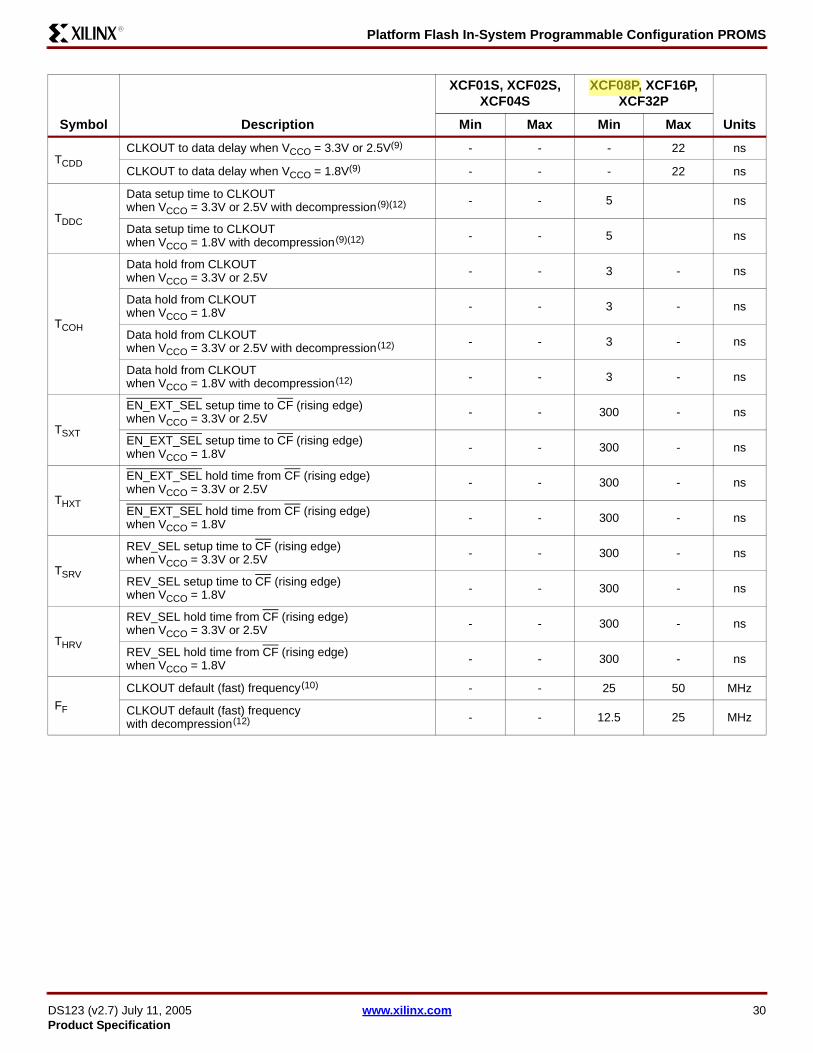
Platform Flash In-System Programmable Configuration PROMS
DS123 (v27) July 11 2005 wwwxilinxcom 31Product Specification
R
FS
CLKOUT alternate (slower) frequency(11) - - 125 25 MHz
CLKOUT alternate (slower) frequency with decompression(12) - - 6 125 MHz
Notes 1 AC test load = 50 pF for XCF01SXCF02SXCF04S 30 pF for XCF08PXCF16PXCF32P2 Float delays are measured with 5 pF AC loads Transition is measured at plusmn200 mV from steady-state active levels3 Guaranteed by design not tested4 All AC parameters are measured with VIL = 00V and VIH = 30V5 If THCE High lt 2 micros TCE = 2 micros6 If THOE Low lt 2 micros TOE = 2 micros7 This is the minimum possible TCYC Actual TCYC = TCAC + FPGA Data setup time
Example With the XCF32P in serial mode with VCCO at 33V if FPGA Data setup time = 15 ns then the actual TCYC = 25 ns +15 ns = 40 ns8 The delay before the enabled CLKOUT signal begins clocking data out of the device is dependent on the clocking configuration The delay before
CLKOUT is enabled will increase if decompression is enabled 9 Slower CLK frequency option may be required to meet the FPGA data sheet setup time10 Typical CLKOUT default (fast) period = 25 ns (40 MHz)11 Typical CLKOUT alternate (slower) period = 50 ns (20 MHz)12 When decompression is enabled the CLKOUT signal becomes a controlled clock output When decompressed data is available CLKOUT will toggle
at frac12 the source clock frequency (either frac12 the selected internal clock frequency or frac12 the external CLK input frequency) When decompressed data is not available the CLKOUT pin is parked High If CLKOUT is used then it must be pulled High externally using a 47kΩ pull-up to VCCO
Symbol Description
XCF01S XCF02S XCF04S
XCF08P XCF16P XCF32P
UnitsMin Max Min Max
huffman
XCF08P
huffman
XCF08P
Platform Flash In-System Programmable Configuration PROMS
DS123 (v27) July 11 2005 wwwxilinxcom 32Product Specification
R
AC Characteristics Over Operating Conditions When Cascading
Symbol Description
XCF01S XCF02S XCF04S
XCF08P XCF16P XCF32P
UnitsMin Max Min Max
TCDF
CLK to output float delay(23) when VCCO = 25V or 33V - 25 - 20 ns
CLK to output float delay(23) when VCCO = 18V - 35 - 20 ns
TOCKCLK to CEO delay(35) when VCCO = 25V or 33V - 20 - 20 ns
CLK to CEO delay(35) when VCCO = 18V - 35 - 20 ns
TOCECE to CEO delay(36) when VCCO = 25V or 33V - 20 - 80 ns
CE to CEO delay(36) when VCCO = 18V - 35 - 80 ns
TOOEOERESET to CEO delay(3) when VCCO = 25V or 33V - 20 - 80 ns
OERESET to CEO delay(3) when VCCO = 18V - 35 - 80 ns
TCOCECLKOUT to CEO delay when VCCO = 25V or 33V - - - 20 ns
CLKOUT to CEO delay when VCCO = 18V - - - 20 ns
TCODF
CLKOUT to output float delay when VCCO = 25V or 33V - - - 25 ns
CLKOUT to output float delay when VCCO = 18V - - - 25 ns
Notes 1 AC test load = 50 pF for XCF01SXCF02SXCF04S 30 pF for XCF08PXCF16PXCF32P2 Float delays are measured with 5 pF AC loads Transition is measured at plusmn200 mV from steady state active levels3 Guaranteed by design not tested4 All AC parameters are measured with VIL = 00V and VIH = 30V5 For cascaded PROMs if the FPGArsquos dual-purpose configuration data pins are set to persist as configuration pins the minimum period is increased
based on the CLK to CEO and CE to data propagation delays- TCYC minimum = TOCK + TCE + FPGA Data setup time- TCAC maximum = TOCK + TCE
6 For cascaded PROMs if the FPGArsquos dual-purpose configuration data pins become general IO pins after configuration to allow for the disable to propagate to the cascaded PROMs and to avoid contention on the data lines following configuration the minimum period is increased based on the CE to CEO and CE to data propagation delays- TCYC minimum = TOCE + TCE - TCAC maximum = TOCK + TCE
OERESET
CE
CLK
CLKOUT(optional)
DATA
CEO
TOCETOOE
First BitLast Bit
TCDFTCODF
TOCK TCOCE
ds123_23_102203
huffman
XCF08P
huffman
XCF08P
Platform Flash In-System Programmable Configuration PROMS
DS123 (v27) July 11 2005 wwwxilinxcom 33Product Specification
R
Pinouts and Pin DescriptionsThe XCFxxS Platform Flash PROM is available in the VO20 and VOG20 packages The XCFxxP Platform Flash PROM isavailable in the VO48 VOG48 FS48 and FSG48 packages This section includes
bull Table 11 XCFxxS Pin Names and Descriptions page 33bull Figure 17 VO20VOG20 Pinout Diagram (Top View) with Pin Names page 34bull Table 12 XCFxxP Pin Names and Descriptions page 35bull Figure 18 VO48VOG48 Pinout Diagram (Top View) with Pin Names page 36bull Table 13 FS48FSG48 Pin NumberName Reference page 38bull Figure 19 FS48FSG48 Pinout Diagram (Top View) page 38
Notes 1 VO20VOG20 denotes a 20-pin (TSSOP) Plastic Thin Shrink Small Outline Package 2 VO48VOG48 denotes a 48-pin (TSOP) Plastic Thin Small Outline Package3 FS48FSG48 denotes a 48-pin (TFBGA) Plastic Thin Fine Pitch Ball Grid Array (08 mm pitch)
XCFxxS Pinouts and Pin DescriptionsTable 11 provides a list of the pin names and descriptions for the XCFxxS 20-pin VO20VOG20 package
Table 11 XCFxxS Pin Names and Descriptions
Pin NameBoundary
Scan OrderBoundary
Scan Function Pin Description20-pin TSSOP (VO20VOG20)
D04 Data Out D0 is the DATA output pin to provide data for configuring an
FPGA in serial mode The D0 output is set to a high-impedance state during ISPEN (when not clamped)
13 Output Enable
CLK 0 Data InConfiguration Clock Input Each rising edge on the CLK input increments the internal address counter if the CLK input is selected CE is Low and OERESET is High
3
OERESET
20 Data In Output EnableReset (Open-Drain IO) When Low this input holds the address counter reset and the DATA output is in a high-impedance state This is a bidirectional open-drain pin that is held Low while the PROM is reset Polarity is not programmable
819 Data Out
18 Output Enable
CE 15 Data InChip Enable Input When CE is High the device is put into low-power standby mode the address counter is reset and the DATA pins are put in a high-impedance state
10
CF22 Data Out Configuration Pulse (Open-Drain Output) Allows JTAG
CONFIG instruction to initiate FPGA configuration without powering down FPGA This is an open-drain output that is pulsed Low by the JTAG CONFIG command
721 Output Enable
CEO
12 Data OutChip Enable Output Chip Enable Output (CEO) is connected to the CE input of the next PROM in the chain This output is Low when CE is Low and OERESET input is High AND the internal address counter has been incremented beyond its Terminal Count (TC) value CEO returns to High when OERESET goes Low or CE goes High
13
11 Output Enable
TMS Mode Select
JTAG Mode Select Input The state of TMS on the rising edge of TCK determines the state transitions at the Test Access Port (TAP) controller TMS has an internal 50KΩ resistive pull-up to VCCJ to provide a logic 1 to the device if the pin is not driven
5
TCK ClockJTAG Clock Input This pin is the JTAG test clock It sequences the TAP controller and all the JTAG test and programming electronics
6
Platform Flash In-System Programmable Configuration PROMS
DS123 (v27) July 11 2005 wwwxilinxcom 34Product Specification
R
XCFxxS Pinout Diagram
TDI Data In
JTAG Serial Data Input This pin is the serial input to all JTAG instruction and data registers TDI has an internal 50KΩ resistive pull-up to VCCJ to provide a logic 1 to the device if the pin is not driven
4
TDO Data Out
JTAG Serial Data Output This pin is the serial output for all JTAG instruction and data registers TDO has an internal 50KΩ resistive pull-up to VCCJ to provide a logic 1 to the system if the pin is not driven
17
VCCINT +33V Supply Positive 33V supply voltage for internal logic 18
VCCO+33V 25V or 18V IO Supply Positive 33V 25V or 18V supply voltage connected to the output voltage drivers and input buffers
19
VCCJ+33V or 25V JTAG IO Supply Positive 33V 25V or 18V supply voltage connected to the TDO output voltage driver and TCK TMS and TDI input buffers
20
GND Ground 11
DNC Do not connect (These pins must be left unconnected) 2 9 12 14 15 16
Figure 17 VO20VOG20 Pinout Diagram (Top View) with Pin Names
Table 11 XCFxxS Pin Names and Descriptions (Continued)
Pin NameBoundary
Scan OrderBoundary
Scan Function Pin Description20-pin TSSOP (VO20VOG20)
VO20VOG20Top View
ds123_02_071304
1
2
3
4
5
6
7
8
9
10
20
19
18
17
16
15
14
13
12
11
D0
(DNC)
CLK
TDI
TMS
TCK
CF
OERESET
(DNC)
CE
VCCJ
VCCO
VCCINT
TDO
(DNC)
(DNC)
CEO
(DNC)
GND
(DNC)
Platform Flash In-System Programmable Configuration PROMS
DS123 (v27) July 11 2005 wwwxilinxcom 35Product Specification
R
XCFxxP Pinouts and Pin DescriptionsTable 12 provides a list of the pin names and descriptions for the XCFxxP 48-pin VO48VOG48 and 48-pin FS48FSG48packages
Table 12 XCFxxP Pin Names and Descriptions
Pin Name
Boundary Scan Order
Boundary Scan
Function Pin Description
48-pin TSOP (VO48VOG48)
48-pin TFBGA (FS48FSG48)
D028 Data Out
D0 is the DATA output pin to provide data for configuring an FPGA in serial mode D0-D7 are the DATA output pins to provide parallel data for configuring a Xilinx FPGA in SelectMap (parallel) mode The D0 output is set to a high-impedance state during ISPEN (when not clamped)The D1-D7 outputs are set to a high-impedance state during ISPEN (when not clamped) and when serial mode is selected for configuration The D1-D7 pins can be left unconnected when the PROM is used in serial mode
28 H627 Output Enable
D126 Data Out
29 H525 Output Enable
D224 Data Out
32 E523 Output Enable
D322 Data Out
33 D521 Output Enable
D420 Data Out
43 C519 Output Enable
D518 Data Out
44 B517 Output Enable
D616 Data Out
47 A515 Output Enable
D714 Data Out
48 A613 Output Enable
CLK 01 Data In
Configuration Clock Input An internal programmable control bit selects between the internal oscillator and the CLK input pin as the clock source to control the configuration sequence Each rising edge on the CLK input increments the internal address counter if the CLK input is selected CE is Low OERESET is High BUSY is Low (parallel mode only) and CF is High
12 B3
OERESET
04 Data In Output EnableReset (Open-Drain IO)When Low this input holds the address counter reset and the DATA and CLKOUT outputs are placed in a high-impedance state This is a bidirectional open-drain pin that is held Low while the PROM is reset Polarity is not programmable
11 A303 Data Out
02 Output Enable
CE 00 Data In
Chip Enable Input When CE is High the device is put into low-power standby mode the address counter is reset and the DATA and CLKOUT outputs are placed in a high-impedance state
13 B4
CF
11 Data InConfiguration Pulse (Open-Drain IO) As an output this pin allows the JTAG CONFIG instruction to initiate FPGA configuration without powering down the FPGA This is an open-drain signal that is pulsed Low by the JTAG CONFIG command As an input on the rising edge of CF the current design revision selection is sampled and the internal address counter is reset to the start address for the selected revision If unused the CF pin should be pulled High using an external 47KΩ pull-up to VCCO
6 D110 Data Out
09 Output Enable
Platform Flash In-System Programmable Configuration PROMS
DS123 (v27) July 11 2005 wwwxilinxcom 36Product Specification
R
CEO
06 Data OutChip Enable Output Chip Enable Output (CEO) is connected to the CE input of the next PROM in the chain This output is Low when CE is Low and OERESET input is High AND the internal address counter has been incremented beyond its Terminal Count (TC) value CEO returns to High when OERESET goes Low or CE goes High
10 D2
05 Output Enable
EN_EXT_SEL 31 Data In
Enable External Selection Input When this pin is Low design revision selection is controlled by the Revision Select pins When this pin is High design revision selection is controlled by the internal programmable Revision Select control bits EN_EXT_SEL has an internal 50KΩ resistive pull-up to VCCO to provide a logic 1 to the device if the pin is not driven
25 H4
REV_SEL0 30 Data InRevision Select[10] Inputs When the EN_EXT_SEL is Low the Revision Select pins are used to select the design revision to be enabled overriding the internal programmable Revision Select control bits The Revision Select[10] inputs have an internal 50KΩ resistive pull-up to VCCO to provide a logic 1 to the device if the pins are not driven
26 G3
REV_SEL1 29 Data In 27 G4
BUSY 12 Data In
Busy Input The BUSY input is enabled when parallel mode is selected for configuration When BUSY is High the internal address counter stops incrementing and the current data remains on the data pins On the first rising edge of CLK after BUSY transitions from High to Low the data for the next address is driven on the data pins When serial mode or decompression is enabled during device programming the BUSY input is disabled BUSY has an internal 50KΩ resistive pull-down to GND to provide a logic 0 to the device if the pin is not driven
5 C1
CLKOUT
08 Data Out
Configuration Clock Output An internal Programmable control bit enables the CLKOUT signal which is sourced from either the internal oscillator or the CLK input pin Each rising edge of the selected clock source increments the internal address counter if data is available CE is Low and OERESET is High Output data is available on the rising edge of CLKOUT CLKOUT is disabled if CE is High or OERESET is Low If decompression is enabled CLKOUT is parked High when decompressed data is not ready When CLKOUT is disabled the CLKOUT pin is put into a high-Z state If CLKOUT is used then it must be pulled High externally using a 47KΩ pull-up to VCCO
9 C2
07 Output Enable
TMS Mode Select
JTAG Mode Select Input The state of TMS on the rising edge of TCK determines the state transitions at the Test Access Port (TAP) controller TMS has an internal 50KΩ resistive pull-up to VCCJ to provide a logic 1 to the device if the pin is not driven
21 E2
TCK ClockJTAG Clock Input This pin is the JTAG test clock It sequences the TAP controller and all the JTAG test and programming electronics
20 H3
TDI Data In
JTAG Serial Data Input This pin is the serial input to all JTAG instruction and data registers TDI has an internal 50KΩ resistive pull-up to VCCJ to provide a logic 1 to the device if the pin is not driven
19 G1
Table 12 XCFxxP Pin Names and Descriptions (Continued)
Pin Name
Boundary Scan Order
Boundary Scan
Function Pin Description
48-pin TSOP (VO48VOG48)
48-pin TFBGA (FS48FSG48)
Platform Flash In-System Programmable Configuration PROMS
DS123 (v27) July 11 2005 wwwxilinxcom 37Product Specification
R
XCFxxP Pinout Diagrams
Figure 18 VO48VOG48 Pinout Diagram (Top View) with Pin Names
TDO Data Out
JTAG Serial Data Output This pin is the serial output for all JTAG instruction and data registers TDO has an internal 50KΩ resistive pull-up to VCCJ to provide a logic 1 to the system if the pin is not driven
22 E6
VCCINT +18V Supply Positive 18V supply voltage for internal logic 4 15 34
B1 E1 G6
VCCO+33V 25V or 18V IO Supply Positive 33V 25V or 18V supply voltage connected to the output voltage drivers and input buffers
8 30 38 45
B2 C6 D6 G5
VCCJ+33V or 25V JTAG IO Supply Positive 33V 25V or 18V supply voltage connected to the TDO output voltage driver and TCK TMS and TDI input buffers
24 H2
GND Ground2 7
17 23 31 36
46
A1 A2 B6 F1 F5 F6
H1
DNC Do Not Connect (These pins must be left unconnected)
1 3 14 16 18 35 37 39 40 41
42
A4 C3 C4 D3 D4 E3 E4 F2 F3 F4
G2
Table 12 XCFxxP Pin Names and Descriptions (Continued)
Pin Name
Boundary Scan Order
Boundary Scan
Function Pin Description
48-pin TSOP (VO48VOG48)
48-pin TFBGA (FS48FSG48)
123456789101112131415161718192021222324
484746454443424140393837363534333231302928272625
VO48VOG48Top View
DNCGNDDNC
VCCINTBUSY
CFGND
VCCOCLKOUT
CEOOERESET
CLKCE
DNCVCCINT
DNCGNDDNCTDI
TCKTMSTDOGND
D7D6GNDVCCOD5D4DNCDNCDNCDNCVCCODNCGNDDNCVCCINTD3D2GNDVCCOD1D0REV_SEL1REV_SEL0EN_EXT_SELVCCJ
Platform Flash In-System Programmable Configuration PROMS
DS123 (v27) July 11 2005 wwwxilinxcom 38Product Specification
R
Table 13 FS48FSG48 Pin NumberName ReferencePin
Number Pin NamePin
Number Pin NameA1 GND E1 VCCINT
A2 GND E2 TMS
A3 OERESET E3 DNC
A4 DNC E4 DNC
A5 D6 E5 D2
A6 D7 E6 TDO
B1 VCCINT F1 GND
B2 VCCO F2 DNC
B3 CLK F3 DNC
B4 CE F4 DNC
B5 D5 F5 GND
B6 GND F6 GND
C1 BUSY G1 TDI
C2 CLKOUT G2 DNC
C3 DNC G3 REV_SEL0
C4 DNC G4 REV_SEL1
C5 D4 G5 VCCO
C6 VCCO G6 VCCINT
D1 CF H1 GND
D2 CEO H2 VCCJ
D3 DNC H3 TCK
D4 DNC H4 EN_EXT_SEL
D5 D3 H5 D1
D6 VCCO H6 D0
Table 13 FS48FSG48 Pin NumberName ReferencePin
Number Pin NamePin
Number Pin Name
1 2 3 4 5 6
ds121_01_071604
A
B
C
D
E
F
G
H
FS48FSG48Top View
Platform Flash In-System Programmable Configuration PROMS
DS123 (v27) July 11 2005 wwwxilinxcom 39Product Specification
R
Ordering Information
Valid Ordering Combinations
Marking Information
XCF01SVO20 C XCF08PVO48 C XCF08PFS48 C XCF01SVOG20 C XCF08PVOG48 C XCF08PFSG48 C
XCF02SVO20 C XCF16PVO48 C XCF16PFS48 C XCF02SVOG20 C XCF16PVOG48 C XCF16PFSG48 C
XCF04SVO20 C XCF32PVO48 C XCF32PFS48 C XCF04SVOG20 C XCF32PVOG48 C XCF32PFSG48 C
XCF04S VO20 C
Operating RangeProcessingC = (TA = ndash40degC to +85degC)Package Type
VO20 = 20-pin TSSOP PackageVOG20 = 20-pin TSSOP Package Pb-free
Device NumberXCF01SXCF02SXCF04S
XCF32P FS48 C
Operating RangeProcessingC = (TA = ndash40degC to +85degC)Package Type
VO48 = 48-pin TSOP PackageVOG48 = 48-pin TSOP Package Pb-freeFS48 = 48-pin TFBGA PackageFSG48 = 48-pin TFBGA Package Pb-free
Device NumberXCF08PXCF16PXCF32P
XCF04S-V
Operating RangeProcessingC = (TA = ndash40degC to +85degC)Package Type
V = 20-pin TSSOP Package (VO20)VG = 20-pin TSSOP Package Pb-free (VOG20)VO48 = 48-pin TSOP Package (VO48)VOG48 = 48-pin TSOP Package Pb-free (VOG48)F48 = 48-pin TFBGA Package (FS48)FG48 = 48-pin TFBGA Package Pb-free (FSG48)
Device NumberXCF01SXCF02SXCF04SXCF08PXCF16PXCF32P
huffman
XCF08PFS48 C
huffman
XCF08P
huffman
XCF08P
Platform Flash In-System Programmable Configuration PROMS
DS123 (v27) July 11 2005 wwwxilinxcom 40Product Specification
R
Revision HistoryThe following table shows the revision history for this document
Date Version Revision
042903 10 Xilinx Initial Release
060303 11 Made edits to all pages
110503 20 Major revision
111803 21 Pinout corrections as followsbull Table 12
- For VO48 package removed 38 from VCCINT and added it to VCCO- For FS48 package removed pin D6 from VCCINT and added it to VCCO
bull Table 13 (FS48 package) - For pin D6 changed name from VCCINT to VCCO- For pin A4 changed name from GND to DNC
bull Figure 18 (VO48 package) For pin 38 changed name from VCCINT to VCCO
121503 22 bull Added specification (47kΩ) for recommended pull-up resistor on OERESET pin to section Reset and Power-On Reset Activation page 22
bull Added paragraph to section Standby Mode page 22 concerning use of a pull-up resistor andor buffer on the DONE pin
050704 23 bull Section Features page 1 Added package styles and 33 MHz configuration speed limit to itemized features
bull Section Description page 1 and following Added state conditions for CF and BUSY to the descriptive text
bull Table 2 page 3 Updated Virtex-II configuration bitstream sizesbull Section Design Revisioning page 9 Rewrittenbull Section PROM to FPGA Configuration Mode and Connections Summary
page 10 and following five instances Added instruction to tie CF High if it is not tied to the FPGArsquos PROG_B (PROGRAM) input
bull Figure 8 page 14 through Figure 15 page 21 Added footnote indicating the directionality of the CF pin in each configuration
bull Section IO Input Voltage Tolerance and Power Sequencing page 22 Rewrittenbull Table 10 page 23 Added CF column to truth table and added an additional row to
document the Low state of CFbull Section Absolute Maximum Ratings page 24 Revised VIN and VTS for rsquoPrsquo
devices bull Section Supply Voltage Requirements for Power-On Reset and Power-Down
page 24- Revised footnote callout number on TOER from Footnote (4) to Footnote (3)- Added Footnote (2) callout to TVCC
bull Section Recommended Operating Conditions page 25 - Added Typical (Typ) parameter columns and parameters for VCCINT and
VCCOVCCJ- Added 15V operation parameter row to VIL and VIH rsquoPrsquo devices- Revised VIH Min 25V operation from 20V to 17V- Added parameter row TIN and Max parameters
bull (Continued on next page)
Platform Flash In-System Programmable Configuration PROMS
DS123 (v27) July 11 2005 wwwxilinxcom 41Product Specification
R
050704(contrsquod)
23(contrsquod)
bull Section DC Characteristics Over Operating Conditions page 26 - Added parameter row and parameters for parallel configuration mode rsquoPrsquo
devices to ICCO- Added Footnote (1) and Footnote (2) with callouts in the Test Conditions column
for ICCJ ICCINTS ICCOS and ICCJS to define active and standby mode requirements
bull Section AC Characteristics Over Operating Conditions page 28 - Corrected description for second TCAC parameter line to show parameters for
18V VCCO- Revised Footnote (7) to indicate VCCO = 33V- Applied Footnote (7) to second TCYC parameter line
bull Section AC Characteristics Over Operating Conditions When Cascading page 32 Revised Footnote (5)TCYC Min and TCAC Min formulas
bull Table 12 page 35 - Added additional state conditions to CLK description- Added function of resetting the internal address counter to CF description
072004 24 bull Added Pb-free package options VOG20 FSG48 and VOG48bull Figure 8 page 14 and Figure 9 page 15 Corrected connection name for FPGA
DOUT (OPTIONAL Daisy-chained Slave FPGAs with different configurations) from DOUT to DIN
bull Section Absolute Maximum Ratings page 24 Removed parameter TSOL from table (TSOL information can be found in Package User Guide)
bull Table 2 page 3 Removed reference to XC2VP125 FPGA
101804 25 bull Table 1 page 1 Broke out VCCO VCCJ into two separate columnsbull Table 7 page 7 Added clarification of ID code die revision bitsbull Table 8 page 8 Deleted TCKMIN2 (bypass mode) and renamed TCKMIN1 to TCKMINbull Table Recommended Operating Conditions page 25 Separated VCCO and VCCJ
parametersbull Table DC Characteristics Over Operating Conditions page 26
- Added most parameter values for XCF08P XCF16P XCF32P devices- Added Footnote (1) to ICCO specifying no-load conditions
bull Table AC Characteristics Over Operating Conditions page 28 - Added most parameter values for XCF08P XCF16P XCF32P devices- Expanded Footnote (1) to include XCF08P XCF16P XCF32P devices- Added Footnote (8) through (11) relating to CLKOUT conditions for various
parameters- Added rows to TCYC specifying parameters for parallel mode- Added rows specifying parameters with decompression for TCLKO TCOH TFF
TSF- Added TDDC (setup time with decompression)
bull Table AC Characteristics Over Operating Conditions When Cascading page 32 - Added most parameter values for XCF08P XCF16P XCF32P devices- Separated Footnote (5) into Footnotes (5) and (6) to specify different
derivations of TCYC depending on whether dual-purpose configuration pins persist as configuration pins or become general IO pins after configuration
huffman
XCF08P
huffman
XCF08P
huffman
XCF08P
huffman
XCF08P
Platform Flash In-System Programmable Configuration PROMS
DS123 (v27) July 11 2005 wwwxilinxcom 42Product Specification
R
031405 26 bull Added Virtex-4 LXFXSX configuration data to Table 2 bull Corrected Virtex-II configuration data in Table 2bull Corrected Virtex-II Pro configuration data in Table 2bull Added Spartan-3L configuration data to Table 2bull Added Spartan-3E configuration data to Table 2bull Paragraph added to FPGA Master SelectMAP (Parallel) Mode (1) page 11bull Changes to DC Characteristics
- TOER changed page 26- IOL changed for VOL page 26- VCCO added to test conditions for IIL IILP IIHPand IIH page 26 Values modified
for IILP and IIHPbull Changes to AC Characteristics
- TLC and THC modified for 18V page 29- New rows added for TCEC and TOEC page 29
bull Minor changes to grammar and punctuationbull Add explanation of Preliminary to DC and AC Electrical Characteristics
071105 27 bull Move from Preliminary to Product Specificationbull Corrections to Virtex-4 configuration bitstream valuesbull Minor changes to figures 9 14 15 and 18bull Change to Internal Oscillator description page 8bull Change to CLKOUT description page 8
- Platform Flash In-System Programmable Configuration PROMS
-
- Features
- Description
- Programming
-
- In-System Programming
-
- OERESET
-
- External Programming
- Reliability and Endurance
-
- Design Security
-
- Read Protection
- Write Protection
-
- IEEE 11491 Boundary-Scan (JTAG)
-
- Instruction Register
-
- XCFxxS Instruction Register (8 bits wide)
- XCFxxP Instruction Register (16 bits wide)
-
- Boundary Scan Register
- Identification Registers
-
- IDCODE Register
- USERCODE Register
- Customer Code Register
-
- Platform Flash PROM TAP Characteristics
-
- TAP Timing
- TAP AC Parameters
-
- Additional Features for the XCFxxP
-
- Internal Oscillator
- CLKOUT
- Decompression
- Design Revisioning
-
- PROM to FPGA Configuration Mode and Connections Summary
-
- FPGA Master Serial Mode
- FPGA Slave Serial Mode
- Serial Daisy Chain
- FPGA Master SelectMAP (Parallel) Mode
- FPGA Slave SelectMAP (Parallel) Mode
- FPGA SelectMAP (Parallel) Device Chaining
- Cascading Configuration PROMs
- Initiating FPGA Configuration
-
- Configuration PROM to FPGA Device Interface Connection Diagrams
- Reset and Power-On Reset Activation
- IO Input Voltage Tolerance and Power Sequencing
- Standby Mode
- DC Electrical Characteristics
- AC Electrical Characteristics
-
- Absolute Maximum Ratings
- Supply Voltage Requirements for Power-On Reset and Power-Down
- Recommended Operating Conditions
- Quality and Reliability Characteristics
- DC Characteristics Over Operating Conditions
- AC Characteristics Over Operating Conditions
- AC Characteristics Over Operating Conditions When Cascading
-
- Pinouts and Pin Descriptions
-
- XCFxxS Pinouts and Pin Descriptions
- XCFxxS Pinout Diagram
- XCFxxP Pinouts and Pin Descriptions
- XCFxxP Pinout Diagrams
-
- Ordering Information
- Valid Ordering Combinations
- Marking Information
- Revision History
-
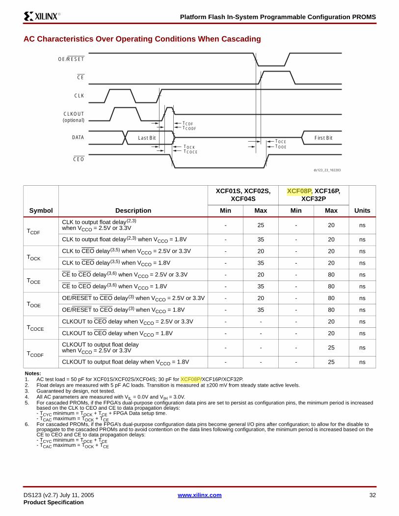
Platform Flash In-System Programmable Configuration PROMS
DS123 (v27) July 11 2005 wwwxilinxcom 32Product Specification
R
AC Characteristics Over Operating Conditions When Cascading
Symbol Description
XCF01S XCF02S XCF04S
XCF08P XCF16P XCF32P
UnitsMin Max Min Max
TCDF
CLK to output float delay(23) when VCCO = 25V or 33V - 25 - 20 ns
CLK to output float delay(23) when VCCO = 18V - 35 - 20 ns
TOCKCLK to CEO delay(35) when VCCO = 25V or 33V - 20 - 20 ns
CLK to CEO delay(35) when VCCO = 18V - 35 - 20 ns
TOCECE to CEO delay(36) when VCCO = 25V or 33V - 20 - 80 ns
CE to CEO delay(36) when VCCO = 18V - 35 - 80 ns
TOOEOERESET to CEO delay(3) when VCCO = 25V or 33V - 20 - 80 ns
OERESET to CEO delay(3) when VCCO = 18V - 35 - 80 ns
TCOCECLKOUT to CEO delay when VCCO = 25V or 33V - - - 20 ns
CLKOUT to CEO delay when VCCO = 18V - - - 20 ns
TCODF
CLKOUT to output float delay when VCCO = 25V or 33V - - - 25 ns
CLKOUT to output float delay when VCCO = 18V - - - 25 ns
Notes 1 AC test load = 50 pF for XCF01SXCF02SXCF04S 30 pF for XCF08PXCF16PXCF32P2 Float delays are measured with 5 pF AC loads Transition is measured at plusmn200 mV from steady state active levels3 Guaranteed by design not tested4 All AC parameters are measured with VIL = 00V and VIH = 30V5 For cascaded PROMs if the FPGArsquos dual-purpose configuration data pins are set to persist as configuration pins the minimum period is increased
based on the CLK to CEO and CE to data propagation delays- TCYC minimum = TOCK + TCE + FPGA Data setup time- TCAC maximum = TOCK + TCE
6 For cascaded PROMs if the FPGArsquos dual-purpose configuration data pins become general IO pins after configuration to allow for the disable to propagate to the cascaded PROMs and to avoid contention on the data lines following configuration the minimum period is increased based on the CE to CEO and CE to data propagation delays- TCYC minimum = TOCE + TCE - TCAC maximum = TOCK + TCE
OERESET
CE
CLK
CLKOUT(optional)
DATA
CEO
TOCETOOE
First BitLast Bit
TCDFTCODF
TOCK TCOCE
ds123_23_102203
huffman
XCF08P
huffman
XCF08P
Platform Flash In-System Programmable Configuration PROMS
DS123 (v27) July 11 2005 wwwxilinxcom 33Product Specification
R
Pinouts and Pin DescriptionsThe XCFxxS Platform Flash PROM is available in the VO20 and VOG20 packages The XCFxxP Platform Flash PROM isavailable in the VO48 VOG48 FS48 and FSG48 packages This section includes
bull Table 11 XCFxxS Pin Names and Descriptions page 33bull Figure 17 VO20VOG20 Pinout Diagram (Top View) with Pin Names page 34bull Table 12 XCFxxP Pin Names and Descriptions page 35bull Figure 18 VO48VOG48 Pinout Diagram (Top View) with Pin Names page 36bull Table 13 FS48FSG48 Pin NumberName Reference page 38bull Figure 19 FS48FSG48 Pinout Diagram (Top View) page 38
Notes 1 VO20VOG20 denotes a 20-pin (TSSOP) Plastic Thin Shrink Small Outline Package 2 VO48VOG48 denotes a 48-pin (TSOP) Plastic Thin Small Outline Package3 FS48FSG48 denotes a 48-pin (TFBGA) Plastic Thin Fine Pitch Ball Grid Array (08 mm pitch)
XCFxxS Pinouts and Pin DescriptionsTable 11 provides a list of the pin names and descriptions for the XCFxxS 20-pin VO20VOG20 package
Table 11 XCFxxS Pin Names and Descriptions
Pin NameBoundary
Scan OrderBoundary
Scan Function Pin Description20-pin TSSOP (VO20VOG20)
D04 Data Out D0 is the DATA output pin to provide data for configuring an
FPGA in serial mode The D0 output is set to a high-impedance state during ISPEN (when not clamped)
13 Output Enable
CLK 0 Data InConfiguration Clock Input Each rising edge on the CLK input increments the internal address counter if the CLK input is selected CE is Low and OERESET is High
3
OERESET
20 Data In Output EnableReset (Open-Drain IO) When Low this input holds the address counter reset and the DATA output is in a high-impedance state This is a bidirectional open-drain pin that is held Low while the PROM is reset Polarity is not programmable
819 Data Out
18 Output Enable
CE 15 Data InChip Enable Input When CE is High the device is put into low-power standby mode the address counter is reset and the DATA pins are put in a high-impedance state
10
CF22 Data Out Configuration Pulse (Open-Drain Output) Allows JTAG
CONFIG instruction to initiate FPGA configuration without powering down FPGA This is an open-drain output that is pulsed Low by the JTAG CONFIG command
721 Output Enable
CEO
12 Data OutChip Enable Output Chip Enable Output (CEO) is connected to the CE input of the next PROM in the chain This output is Low when CE is Low and OERESET input is High AND the internal address counter has been incremented beyond its Terminal Count (TC) value CEO returns to High when OERESET goes Low or CE goes High
13
11 Output Enable
TMS Mode Select
JTAG Mode Select Input The state of TMS on the rising edge of TCK determines the state transitions at the Test Access Port (TAP) controller TMS has an internal 50KΩ resistive pull-up to VCCJ to provide a logic 1 to the device if the pin is not driven
5
TCK ClockJTAG Clock Input This pin is the JTAG test clock It sequences the TAP controller and all the JTAG test and programming electronics
6
Platform Flash In-System Programmable Configuration PROMS
DS123 (v27) July 11 2005 wwwxilinxcom 34Product Specification
R
XCFxxS Pinout Diagram
TDI Data In
JTAG Serial Data Input This pin is the serial input to all JTAG instruction and data registers TDI has an internal 50KΩ resistive pull-up to VCCJ to provide a logic 1 to the device if the pin is not driven
4
TDO Data Out
JTAG Serial Data Output This pin is the serial output for all JTAG instruction and data registers TDO has an internal 50KΩ resistive pull-up to VCCJ to provide a logic 1 to the system if the pin is not driven
17
VCCINT +33V Supply Positive 33V supply voltage for internal logic 18
VCCO+33V 25V or 18V IO Supply Positive 33V 25V or 18V supply voltage connected to the output voltage drivers and input buffers
19
VCCJ+33V or 25V JTAG IO Supply Positive 33V 25V or 18V supply voltage connected to the TDO output voltage driver and TCK TMS and TDI input buffers
20
GND Ground 11
DNC Do not connect (These pins must be left unconnected) 2 9 12 14 15 16
Figure 17 VO20VOG20 Pinout Diagram (Top View) with Pin Names
Table 11 XCFxxS Pin Names and Descriptions (Continued)
Pin NameBoundary
Scan OrderBoundary
Scan Function Pin Description20-pin TSSOP (VO20VOG20)
VO20VOG20Top View
ds123_02_071304
1
2
3
4
5
6
7
8
9
10
20
19
18
17
16
15
14
13
12
11
D0
(DNC)
CLK
TDI
TMS
TCK
CF
OERESET
(DNC)
CE
VCCJ
VCCO
VCCINT
TDO
(DNC)
(DNC)
CEO
(DNC)
GND
(DNC)
Platform Flash In-System Programmable Configuration PROMS
DS123 (v27) July 11 2005 wwwxilinxcom 35Product Specification
R
XCFxxP Pinouts and Pin DescriptionsTable 12 provides a list of the pin names and descriptions for the XCFxxP 48-pin VO48VOG48 and 48-pin FS48FSG48packages
Table 12 XCFxxP Pin Names and Descriptions
Pin Name
Boundary Scan Order
Boundary Scan
Function Pin Description
48-pin TSOP (VO48VOG48)
48-pin TFBGA (FS48FSG48)
D028 Data Out
D0 is the DATA output pin to provide data for configuring an FPGA in serial mode D0-D7 are the DATA output pins to provide parallel data for configuring a Xilinx FPGA in SelectMap (parallel) mode The D0 output is set to a high-impedance state during ISPEN (when not clamped)The D1-D7 outputs are set to a high-impedance state during ISPEN (when not clamped) and when serial mode is selected for configuration The D1-D7 pins can be left unconnected when the PROM is used in serial mode
28 H627 Output Enable
D126 Data Out
29 H525 Output Enable
D224 Data Out
32 E523 Output Enable
D322 Data Out
33 D521 Output Enable
D420 Data Out
43 C519 Output Enable
D518 Data Out
44 B517 Output Enable
D616 Data Out
47 A515 Output Enable
D714 Data Out
48 A613 Output Enable
CLK 01 Data In
Configuration Clock Input An internal programmable control bit selects between the internal oscillator and the CLK input pin as the clock source to control the configuration sequence Each rising edge on the CLK input increments the internal address counter if the CLK input is selected CE is Low OERESET is High BUSY is Low (parallel mode only) and CF is High
12 B3
OERESET
04 Data In Output EnableReset (Open-Drain IO)When Low this input holds the address counter reset and the DATA and CLKOUT outputs are placed in a high-impedance state This is a bidirectional open-drain pin that is held Low while the PROM is reset Polarity is not programmable
11 A303 Data Out
02 Output Enable
CE 00 Data In
Chip Enable Input When CE is High the device is put into low-power standby mode the address counter is reset and the DATA and CLKOUT outputs are placed in a high-impedance state
13 B4
CF
11 Data InConfiguration Pulse (Open-Drain IO) As an output this pin allows the JTAG CONFIG instruction to initiate FPGA configuration without powering down the FPGA This is an open-drain signal that is pulsed Low by the JTAG CONFIG command As an input on the rising edge of CF the current design revision selection is sampled and the internal address counter is reset to the start address for the selected revision If unused the CF pin should be pulled High using an external 47KΩ pull-up to VCCO
6 D110 Data Out
09 Output Enable
Platform Flash In-System Programmable Configuration PROMS
DS123 (v27) July 11 2005 wwwxilinxcom 36Product Specification
R
CEO
06 Data OutChip Enable Output Chip Enable Output (CEO) is connected to the CE input of the next PROM in the chain This output is Low when CE is Low and OERESET input is High AND the internal address counter has been incremented beyond its Terminal Count (TC) value CEO returns to High when OERESET goes Low or CE goes High
10 D2
05 Output Enable
EN_EXT_SEL 31 Data In
Enable External Selection Input When this pin is Low design revision selection is controlled by the Revision Select pins When this pin is High design revision selection is controlled by the internal programmable Revision Select control bits EN_EXT_SEL has an internal 50KΩ resistive pull-up to VCCO to provide a logic 1 to the device if the pin is not driven
25 H4
REV_SEL0 30 Data InRevision Select[10] Inputs When the EN_EXT_SEL is Low the Revision Select pins are used to select the design revision to be enabled overriding the internal programmable Revision Select control bits The Revision Select[10] inputs have an internal 50KΩ resistive pull-up to VCCO to provide a logic 1 to the device if the pins are not driven
26 G3
REV_SEL1 29 Data In 27 G4
BUSY 12 Data In
Busy Input The BUSY input is enabled when parallel mode is selected for configuration When BUSY is High the internal address counter stops incrementing and the current data remains on the data pins On the first rising edge of CLK after BUSY transitions from High to Low the data for the next address is driven on the data pins When serial mode or decompression is enabled during device programming the BUSY input is disabled BUSY has an internal 50KΩ resistive pull-down to GND to provide a logic 0 to the device if the pin is not driven
5 C1
CLKOUT
08 Data Out
Configuration Clock Output An internal Programmable control bit enables the CLKOUT signal which is sourced from either the internal oscillator or the CLK input pin Each rising edge of the selected clock source increments the internal address counter if data is available CE is Low and OERESET is High Output data is available on the rising edge of CLKOUT CLKOUT is disabled if CE is High or OERESET is Low If decompression is enabled CLKOUT is parked High when decompressed data is not ready When CLKOUT is disabled the CLKOUT pin is put into a high-Z state If CLKOUT is used then it must be pulled High externally using a 47KΩ pull-up to VCCO
9 C2
07 Output Enable
TMS Mode Select
JTAG Mode Select Input The state of TMS on the rising edge of TCK determines the state transitions at the Test Access Port (TAP) controller TMS has an internal 50KΩ resistive pull-up to VCCJ to provide a logic 1 to the device if the pin is not driven
21 E2
TCK ClockJTAG Clock Input This pin is the JTAG test clock It sequences the TAP controller and all the JTAG test and programming electronics
20 H3
TDI Data In
JTAG Serial Data Input This pin is the serial input to all JTAG instruction and data registers TDI has an internal 50KΩ resistive pull-up to VCCJ to provide a logic 1 to the device if the pin is not driven
19 G1
Table 12 XCFxxP Pin Names and Descriptions (Continued)
Pin Name
Boundary Scan Order
Boundary Scan
Function Pin Description
48-pin TSOP (VO48VOG48)
48-pin TFBGA (FS48FSG48)
Platform Flash In-System Programmable Configuration PROMS
DS123 (v27) July 11 2005 wwwxilinxcom 37Product Specification
R
XCFxxP Pinout Diagrams
Figure 18 VO48VOG48 Pinout Diagram (Top View) with Pin Names
TDO Data Out
JTAG Serial Data Output This pin is the serial output for all JTAG instruction and data registers TDO has an internal 50KΩ resistive pull-up to VCCJ to provide a logic 1 to the system if the pin is not driven
22 E6
VCCINT +18V Supply Positive 18V supply voltage for internal logic 4 15 34
B1 E1 G6
VCCO+33V 25V or 18V IO Supply Positive 33V 25V or 18V supply voltage connected to the output voltage drivers and input buffers
8 30 38 45
B2 C6 D6 G5
VCCJ+33V or 25V JTAG IO Supply Positive 33V 25V or 18V supply voltage connected to the TDO output voltage driver and TCK TMS and TDI input buffers
24 H2
GND Ground2 7
17 23 31 36
46
A1 A2 B6 F1 F5 F6
H1
DNC Do Not Connect (These pins must be left unconnected)
1 3 14 16 18 35 37 39 40 41
42
A4 C3 C4 D3 D4 E3 E4 F2 F3 F4
G2
Table 12 XCFxxP Pin Names and Descriptions (Continued)
Pin Name
Boundary Scan Order
Boundary Scan
Function Pin Description
48-pin TSOP (VO48VOG48)
48-pin TFBGA (FS48FSG48)
123456789101112131415161718192021222324
484746454443424140393837363534333231302928272625
VO48VOG48Top View
DNCGNDDNC
VCCINTBUSY
CFGND
VCCOCLKOUT
CEOOERESET
CLKCE
DNCVCCINT
DNCGNDDNCTDI
TCKTMSTDOGND
D7D6GNDVCCOD5D4DNCDNCDNCDNCVCCODNCGNDDNCVCCINTD3D2GNDVCCOD1D0REV_SEL1REV_SEL0EN_EXT_SELVCCJ
Platform Flash In-System Programmable Configuration PROMS
DS123 (v27) July 11 2005 wwwxilinxcom 38Product Specification
R
Table 13 FS48FSG48 Pin NumberName ReferencePin
Number Pin NamePin
Number Pin NameA1 GND E1 VCCINT
A2 GND E2 TMS
A3 OERESET E3 DNC
A4 DNC E4 DNC
A5 D6 E5 D2
A6 D7 E6 TDO
B1 VCCINT F1 GND
B2 VCCO F2 DNC
B3 CLK F3 DNC
B4 CE F4 DNC
B5 D5 F5 GND
B6 GND F6 GND
C1 BUSY G1 TDI
C2 CLKOUT G2 DNC
C3 DNC G3 REV_SEL0
C4 DNC G4 REV_SEL1
C5 D4 G5 VCCO
C6 VCCO G6 VCCINT
D1 CF H1 GND
D2 CEO H2 VCCJ
D3 DNC H3 TCK
D4 DNC H4 EN_EXT_SEL
D5 D3 H5 D1
D6 VCCO H6 D0
Table 13 FS48FSG48 Pin NumberName ReferencePin
Number Pin NamePin
Number Pin Name
1 2 3 4 5 6
ds121_01_071604
A
B
C
D
E
F
G
H
FS48FSG48Top View
Platform Flash In-System Programmable Configuration PROMS
DS123 (v27) July 11 2005 wwwxilinxcom 39Product Specification
R
Ordering Information
Valid Ordering Combinations
Marking Information
XCF01SVO20 C XCF08PVO48 C XCF08PFS48 C XCF01SVOG20 C XCF08PVOG48 C XCF08PFSG48 C
XCF02SVO20 C XCF16PVO48 C XCF16PFS48 C XCF02SVOG20 C XCF16PVOG48 C XCF16PFSG48 C
XCF04SVO20 C XCF32PVO48 C XCF32PFS48 C XCF04SVOG20 C XCF32PVOG48 C XCF32PFSG48 C
XCF04S VO20 C
Operating RangeProcessingC = (TA = ndash40degC to +85degC)Package Type
VO20 = 20-pin TSSOP PackageVOG20 = 20-pin TSSOP Package Pb-free
Device NumberXCF01SXCF02SXCF04S
XCF32P FS48 C
Operating RangeProcessingC = (TA = ndash40degC to +85degC)Package Type
VO48 = 48-pin TSOP PackageVOG48 = 48-pin TSOP Package Pb-freeFS48 = 48-pin TFBGA PackageFSG48 = 48-pin TFBGA Package Pb-free
Device NumberXCF08PXCF16PXCF32P
XCF04S-V
Operating RangeProcessingC = (TA = ndash40degC to +85degC)Package Type
V = 20-pin TSSOP Package (VO20)VG = 20-pin TSSOP Package Pb-free (VOG20)VO48 = 48-pin TSOP Package (VO48)VOG48 = 48-pin TSOP Package Pb-free (VOG48)F48 = 48-pin TFBGA Package (FS48)FG48 = 48-pin TFBGA Package Pb-free (FSG48)
Device NumberXCF01SXCF02SXCF04SXCF08PXCF16PXCF32P
huffman
XCF08PFS48 C
huffman
XCF08P
huffman
XCF08P
Platform Flash In-System Programmable Configuration PROMS
DS123 (v27) July 11 2005 wwwxilinxcom 40Product Specification
R
Revision HistoryThe following table shows the revision history for this document
Date Version Revision
042903 10 Xilinx Initial Release
060303 11 Made edits to all pages
110503 20 Major revision
111803 21 Pinout corrections as followsbull Table 12
- For VO48 package removed 38 from VCCINT and added it to VCCO- For FS48 package removed pin D6 from VCCINT and added it to VCCO
bull Table 13 (FS48 package) - For pin D6 changed name from VCCINT to VCCO- For pin A4 changed name from GND to DNC
bull Figure 18 (VO48 package) For pin 38 changed name from VCCINT to VCCO
121503 22 bull Added specification (47kΩ) for recommended pull-up resistor on OERESET pin to section Reset and Power-On Reset Activation page 22
bull Added paragraph to section Standby Mode page 22 concerning use of a pull-up resistor andor buffer on the DONE pin
050704 23 bull Section Features page 1 Added package styles and 33 MHz configuration speed limit to itemized features
bull Section Description page 1 and following Added state conditions for CF and BUSY to the descriptive text
bull Table 2 page 3 Updated Virtex-II configuration bitstream sizesbull Section Design Revisioning page 9 Rewrittenbull Section PROM to FPGA Configuration Mode and Connections Summary
page 10 and following five instances Added instruction to tie CF High if it is not tied to the FPGArsquos PROG_B (PROGRAM) input
bull Figure 8 page 14 through Figure 15 page 21 Added footnote indicating the directionality of the CF pin in each configuration
bull Section IO Input Voltage Tolerance and Power Sequencing page 22 Rewrittenbull Table 10 page 23 Added CF column to truth table and added an additional row to
document the Low state of CFbull Section Absolute Maximum Ratings page 24 Revised VIN and VTS for rsquoPrsquo
devices bull Section Supply Voltage Requirements for Power-On Reset and Power-Down
page 24- Revised footnote callout number on TOER from Footnote (4) to Footnote (3)- Added Footnote (2) callout to TVCC
bull Section Recommended Operating Conditions page 25 - Added Typical (Typ) parameter columns and parameters for VCCINT and
VCCOVCCJ- Added 15V operation parameter row to VIL and VIH rsquoPrsquo devices- Revised VIH Min 25V operation from 20V to 17V- Added parameter row TIN and Max parameters
bull (Continued on next page)
Platform Flash In-System Programmable Configuration PROMS
DS123 (v27) July 11 2005 wwwxilinxcom 41Product Specification
R
050704(contrsquod)
23(contrsquod)
bull Section DC Characteristics Over Operating Conditions page 26 - Added parameter row and parameters for parallel configuration mode rsquoPrsquo
devices to ICCO- Added Footnote (1) and Footnote (2) with callouts in the Test Conditions column
for ICCJ ICCINTS ICCOS and ICCJS to define active and standby mode requirements
bull Section AC Characteristics Over Operating Conditions page 28 - Corrected description for second TCAC parameter line to show parameters for
18V VCCO- Revised Footnote (7) to indicate VCCO = 33V- Applied Footnote (7) to second TCYC parameter line
bull Section AC Characteristics Over Operating Conditions When Cascading page 32 Revised Footnote (5)TCYC Min and TCAC Min formulas
bull Table 12 page 35 - Added additional state conditions to CLK description- Added function of resetting the internal address counter to CF description
072004 24 bull Added Pb-free package options VOG20 FSG48 and VOG48bull Figure 8 page 14 and Figure 9 page 15 Corrected connection name for FPGA
DOUT (OPTIONAL Daisy-chained Slave FPGAs with different configurations) from DOUT to DIN
bull Section Absolute Maximum Ratings page 24 Removed parameter TSOL from table (TSOL information can be found in Package User Guide)
bull Table 2 page 3 Removed reference to XC2VP125 FPGA
101804 25 bull Table 1 page 1 Broke out VCCO VCCJ into two separate columnsbull Table 7 page 7 Added clarification of ID code die revision bitsbull Table 8 page 8 Deleted TCKMIN2 (bypass mode) and renamed TCKMIN1 to TCKMINbull Table Recommended Operating Conditions page 25 Separated VCCO and VCCJ
parametersbull Table DC Characteristics Over Operating Conditions page 26
- Added most parameter values for XCF08P XCF16P XCF32P devices- Added Footnote (1) to ICCO specifying no-load conditions
bull Table AC Characteristics Over Operating Conditions page 28 - Added most parameter values for XCF08P XCF16P XCF32P devices- Expanded Footnote (1) to include XCF08P XCF16P XCF32P devices- Added Footnote (8) through (11) relating to CLKOUT conditions for various
parameters- Added rows to TCYC specifying parameters for parallel mode- Added rows specifying parameters with decompression for TCLKO TCOH TFF
TSF- Added TDDC (setup time with decompression)
bull Table AC Characteristics Over Operating Conditions When Cascading page 32 - Added most parameter values for XCF08P XCF16P XCF32P devices- Separated Footnote (5) into Footnotes (5) and (6) to specify different
derivations of TCYC depending on whether dual-purpose configuration pins persist as configuration pins or become general IO pins after configuration
huffman
XCF08P
huffman
XCF08P
huffman
XCF08P
huffman
XCF08P
Platform Flash In-System Programmable Configuration PROMS
DS123 (v27) July 11 2005 wwwxilinxcom 42Product Specification
R
031405 26 bull Added Virtex-4 LXFXSX configuration data to Table 2 bull Corrected Virtex-II configuration data in Table 2bull Corrected Virtex-II Pro configuration data in Table 2bull Added Spartan-3L configuration data to Table 2bull Added Spartan-3E configuration data to Table 2bull Paragraph added to FPGA Master SelectMAP (Parallel) Mode (1) page 11bull Changes to DC Characteristics
- TOER changed page 26- IOL changed for VOL page 26- VCCO added to test conditions for IIL IILP IIHPand IIH page 26 Values modified
for IILP and IIHPbull Changes to AC Characteristics
- TLC and THC modified for 18V page 29- New rows added for TCEC and TOEC page 29
bull Minor changes to grammar and punctuationbull Add explanation of Preliminary to DC and AC Electrical Characteristics
071105 27 bull Move from Preliminary to Product Specificationbull Corrections to Virtex-4 configuration bitstream valuesbull Minor changes to figures 9 14 15 and 18bull Change to Internal Oscillator description page 8bull Change to CLKOUT description page 8
- Platform Flash In-System Programmable Configuration PROMS
-
- Features
- Description
- Programming
-
- In-System Programming
-
- OERESET
-
- External Programming
- Reliability and Endurance
-
- Design Security
-
- Read Protection
- Write Protection
-
- IEEE 11491 Boundary-Scan (JTAG)
-
- Instruction Register
-
- XCFxxS Instruction Register (8 bits wide)
- XCFxxP Instruction Register (16 bits wide)
-
- Boundary Scan Register
- Identification Registers
-
- IDCODE Register
- USERCODE Register
- Customer Code Register
-
- Platform Flash PROM TAP Characteristics
-
- TAP Timing
- TAP AC Parameters
-
- Additional Features for the XCFxxP
-
- Internal Oscillator
- CLKOUT
- Decompression
- Design Revisioning
-
- PROM to FPGA Configuration Mode and Connections Summary
-
- FPGA Master Serial Mode
- FPGA Slave Serial Mode
- Serial Daisy Chain
- FPGA Master SelectMAP (Parallel) Mode
- FPGA Slave SelectMAP (Parallel) Mode
- FPGA SelectMAP (Parallel) Device Chaining
- Cascading Configuration PROMs
- Initiating FPGA Configuration
-
- Configuration PROM to FPGA Device Interface Connection Diagrams
- Reset and Power-On Reset Activation
- IO Input Voltage Tolerance and Power Sequencing
- Standby Mode
- DC Electrical Characteristics
- AC Electrical Characteristics
-
- Absolute Maximum Ratings
- Supply Voltage Requirements for Power-On Reset and Power-Down
- Recommended Operating Conditions
- Quality and Reliability Characteristics
- DC Characteristics Over Operating Conditions
- AC Characteristics Over Operating Conditions
- AC Characteristics Over Operating Conditions When Cascading
-
- Pinouts and Pin Descriptions
-
- XCFxxS Pinouts and Pin Descriptions
- XCFxxS Pinout Diagram
- XCFxxP Pinouts and Pin Descriptions
- XCFxxP Pinout Diagrams
-
- Ordering Information
- Valid Ordering Combinations
- Marking Information
- Revision History
-
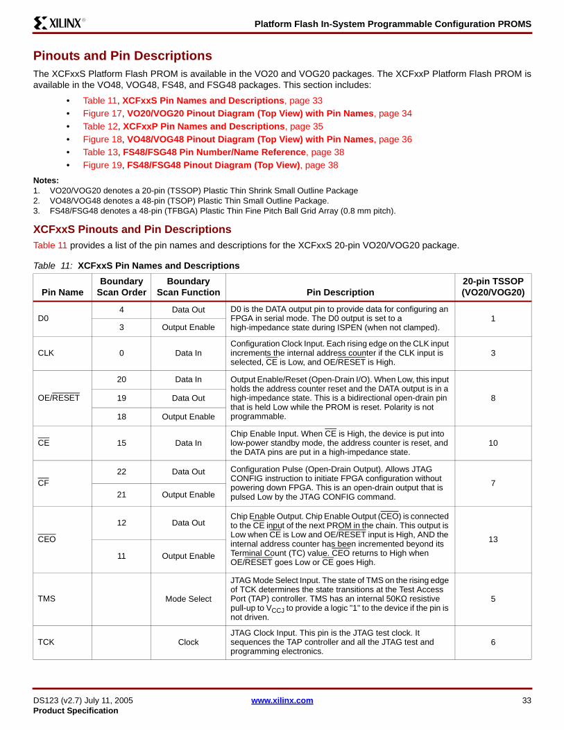
Platform Flash In-System Programmable Configuration PROMS
DS123 (v27) July 11 2005 wwwxilinxcom 33Product Specification
R
Pinouts and Pin DescriptionsThe XCFxxS Platform Flash PROM is available in the VO20 and VOG20 packages The XCFxxP Platform Flash PROM isavailable in the VO48 VOG48 FS48 and FSG48 packages This section includes
bull Table 11 XCFxxS Pin Names and Descriptions page 33bull Figure 17 VO20VOG20 Pinout Diagram (Top View) with Pin Names page 34bull Table 12 XCFxxP Pin Names and Descriptions page 35bull Figure 18 VO48VOG48 Pinout Diagram (Top View) with Pin Names page 36bull Table 13 FS48FSG48 Pin NumberName Reference page 38bull Figure 19 FS48FSG48 Pinout Diagram (Top View) page 38
Notes 1 VO20VOG20 denotes a 20-pin (TSSOP) Plastic Thin Shrink Small Outline Package 2 VO48VOG48 denotes a 48-pin (TSOP) Plastic Thin Small Outline Package3 FS48FSG48 denotes a 48-pin (TFBGA) Plastic Thin Fine Pitch Ball Grid Array (08 mm pitch)
XCFxxS Pinouts and Pin DescriptionsTable 11 provides a list of the pin names and descriptions for the XCFxxS 20-pin VO20VOG20 package
Table 11 XCFxxS Pin Names and Descriptions
Pin NameBoundary
Scan OrderBoundary
Scan Function Pin Description20-pin TSSOP (VO20VOG20)
D04 Data Out D0 is the DATA output pin to provide data for configuring an
FPGA in serial mode The D0 output is set to a high-impedance state during ISPEN (when not clamped)
13 Output Enable
CLK 0 Data InConfiguration Clock Input Each rising edge on the CLK input increments the internal address counter if the CLK input is selected CE is Low and OERESET is High
3
OERESET
20 Data In Output EnableReset (Open-Drain IO) When Low this input holds the address counter reset and the DATA output is in a high-impedance state This is a bidirectional open-drain pin that is held Low while the PROM is reset Polarity is not programmable
819 Data Out
18 Output Enable
CE 15 Data InChip Enable Input When CE is High the device is put into low-power standby mode the address counter is reset and the DATA pins are put in a high-impedance state
10
CF22 Data Out Configuration Pulse (Open-Drain Output) Allows JTAG
CONFIG instruction to initiate FPGA configuration without powering down FPGA This is an open-drain output that is pulsed Low by the JTAG CONFIG command
721 Output Enable
CEO
12 Data OutChip Enable Output Chip Enable Output (CEO) is connected to the CE input of the next PROM in the chain This output is Low when CE is Low and OERESET input is High AND the internal address counter has been incremented beyond its Terminal Count (TC) value CEO returns to High when OERESET goes Low or CE goes High
13
11 Output Enable
TMS Mode Select
JTAG Mode Select Input The state of TMS on the rising edge of TCK determines the state transitions at the Test Access Port (TAP) controller TMS has an internal 50KΩ resistive pull-up to VCCJ to provide a logic 1 to the device if the pin is not driven
5
TCK ClockJTAG Clock Input This pin is the JTAG test clock It sequences the TAP controller and all the JTAG test and programming electronics
6
Platform Flash In-System Programmable Configuration PROMS
DS123 (v27) July 11 2005 wwwxilinxcom 34Product Specification
R
XCFxxS Pinout Diagram
TDI Data In
JTAG Serial Data Input This pin is the serial input to all JTAG instruction and data registers TDI has an internal 50KΩ resistive pull-up to VCCJ to provide a logic 1 to the device if the pin is not driven
4
TDO Data Out
JTAG Serial Data Output This pin is the serial output for all JTAG instruction and data registers TDO has an internal 50KΩ resistive pull-up to VCCJ to provide a logic 1 to the system if the pin is not driven
17
VCCINT +33V Supply Positive 33V supply voltage for internal logic 18
VCCO+33V 25V or 18V IO Supply Positive 33V 25V or 18V supply voltage connected to the output voltage drivers and input buffers
19
VCCJ+33V or 25V JTAG IO Supply Positive 33V 25V or 18V supply voltage connected to the TDO output voltage driver and TCK TMS and TDI input buffers
20
GND Ground 11
DNC Do not connect (These pins must be left unconnected) 2 9 12 14 15 16
Figure 17 VO20VOG20 Pinout Diagram (Top View) with Pin Names
Table 11 XCFxxS Pin Names and Descriptions (Continued)
Pin NameBoundary
Scan OrderBoundary
Scan Function Pin Description20-pin TSSOP (VO20VOG20)
VO20VOG20Top View
ds123_02_071304
1
2
3
4
5
6
7
8
9
10
20
19
18
17
16
15
14
13
12
11
D0
(DNC)
CLK
TDI
TMS
TCK
CF
OERESET
(DNC)
CE
VCCJ
VCCO
VCCINT
TDO
(DNC)
(DNC)
CEO
(DNC)
GND
(DNC)
Platform Flash In-System Programmable Configuration PROMS
DS123 (v27) July 11 2005 wwwxilinxcom 35Product Specification
R
XCFxxP Pinouts and Pin DescriptionsTable 12 provides a list of the pin names and descriptions for the XCFxxP 48-pin VO48VOG48 and 48-pin FS48FSG48packages
Table 12 XCFxxP Pin Names and Descriptions
Pin Name
Boundary Scan Order
Boundary Scan
Function Pin Description
48-pin TSOP (VO48VOG48)
48-pin TFBGA (FS48FSG48)
D028 Data Out
D0 is the DATA output pin to provide data for configuring an FPGA in serial mode D0-D7 are the DATA output pins to provide parallel data for configuring a Xilinx FPGA in SelectMap (parallel) mode The D0 output is set to a high-impedance state during ISPEN (when not clamped)The D1-D7 outputs are set to a high-impedance state during ISPEN (when not clamped) and when serial mode is selected for configuration The D1-D7 pins can be left unconnected when the PROM is used in serial mode
28 H627 Output Enable
D126 Data Out
29 H525 Output Enable
D224 Data Out
32 E523 Output Enable
D322 Data Out
33 D521 Output Enable
D420 Data Out
43 C519 Output Enable
D518 Data Out
44 B517 Output Enable
D616 Data Out
47 A515 Output Enable
D714 Data Out
48 A613 Output Enable
CLK 01 Data In
Configuration Clock Input An internal programmable control bit selects between the internal oscillator and the CLK input pin as the clock source to control the configuration sequence Each rising edge on the CLK input increments the internal address counter if the CLK input is selected CE is Low OERESET is High BUSY is Low (parallel mode only) and CF is High
12 B3
OERESET
04 Data In Output EnableReset (Open-Drain IO)When Low this input holds the address counter reset and the DATA and CLKOUT outputs are placed in a high-impedance state This is a bidirectional open-drain pin that is held Low while the PROM is reset Polarity is not programmable
11 A303 Data Out
02 Output Enable
CE 00 Data In
Chip Enable Input When CE is High the device is put into low-power standby mode the address counter is reset and the DATA and CLKOUT outputs are placed in a high-impedance state
13 B4
CF
11 Data InConfiguration Pulse (Open-Drain IO) As an output this pin allows the JTAG CONFIG instruction to initiate FPGA configuration without powering down the FPGA This is an open-drain signal that is pulsed Low by the JTAG CONFIG command As an input on the rising edge of CF the current design revision selection is sampled and the internal address counter is reset to the start address for the selected revision If unused the CF pin should be pulled High using an external 47KΩ pull-up to VCCO
6 D110 Data Out
09 Output Enable
Platform Flash In-System Programmable Configuration PROMS
DS123 (v27) July 11 2005 wwwxilinxcom 36Product Specification
R
CEO
06 Data OutChip Enable Output Chip Enable Output (CEO) is connected to the CE input of the next PROM in the chain This output is Low when CE is Low and OERESET input is High AND the internal address counter has been incremented beyond its Terminal Count (TC) value CEO returns to High when OERESET goes Low or CE goes High
10 D2
05 Output Enable
EN_EXT_SEL 31 Data In
Enable External Selection Input When this pin is Low design revision selection is controlled by the Revision Select pins When this pin is High design revision selection is controlled by the internal programmable Revision Select control bits EN_EXT_SEL has an internal 50KΩ resistive pull-up to VCCO to provide a logic 1 to the device if the pin is not driven
25 H4
REV_SEL0 30 Data InRevision Select[10] Inputs When the EN_EXT_SEL is Low the Revision Select pins are used to select the design revision to be enabled overriding the internal programmable Revision Select control bits The Revision Select[10] inputs have an internal 50KΩ resistive pull-up to VCCO to provide a logic 1 to the device if the pins are not driven
26 G3
REV_SEL1 29 Data In 27 G4
BUSY 12 Data In
Busy Input The BUSY input is enabled when parallel mode is selected for configuration When BUSY is High the internal address counter stops incrementing and the current data remains on the data pins On the first rising edge of CLK after BUSY transitions from High to Low the data for the next address is driven on the data pins When serial mode or decompression is enabled during device programming the BUSY input is disabled BUSY has an internal 50KΩ resistive pull-down to GND to provide a logic 0 to the device if the pin is not driven
5 C1
CLKOUT
08 Data Out
Configuration Clock Output An internal Programmable control bit enables the CLKOUT signal which is sourced from either the internal oscillator or the CLK input pin Each rising edge of the selected clock source increments the internal address counter if data is available CE is Low and OERESET is High Output data is available on the rising edge of CLKOUT CLKOUT is disabled if CE is High or OERESET is Low If decompression is enabled CLKOUT is parked High when decompressed data is not ready When CLKOUT is disabled the CLKOUT pin is put into a high-Z state If CLKOUT is used then it must be pulled High externally using a 47KΩ pull-up to VCCO
9 C2
07 Output Enable
TMS Mode Select
JTAG Mode Select Input The state of TMS on the rising edge of TCK determines the state transitions at the Test Access Port (TAP) controller TMS has an internal 50KΩ resistive pull-up to VCCJ to provide a logic 1 to the device if the pin is not driven
21 E2
TCK ClockJTAG Clock Input This pin is the JTAG test clock It sequences the TAP controller and all the JTAG test and programming electronics
20 H3
TDI Data In
JTAG Serial Data Input This pin is the serial input to all JTAG instruction and data registers TDI has an internal 50KΩ resistive pull-up to VCCJ to provide a logic 1 to the device if the pin is not driven
19 G1
Table 12 XCFxxP Pin Names and Descriptions (Continued)
Pin Name
Boundary Scan Order
Boundary Scan
Function Pin Description
48-pin TSOP (VO48VOG48)
48-pin TFBGA (FS48FSG48)
Platform Flash In-System Programmable Configuration PROMS
DS123 (v27) July 11 2005 wwwxilinxcom 37Product Specification
R
XCFxxP Pinout Diagrams
Figure 18 VO48VOG48 Pinout Diagram (Top View) with Pin Names
TDO Data Out
JTAG Serial Data Output This pin is the serial output for all JTAG instruction and data registers TDO has an internal 50KΩ resistive pull-up to VCCJ to provide a logic 1 to the system if the pin is not driven
22 E6
VCCINT +18V Supply Positive 18V supply voltage for internal logic 4 15 34
B1 E1 G6
VCCO+33V 25V or 18V IO Supply Positive 33V 25V or 18V supply voltage connected to the output voltage drivers and input buffers
8 30 38 45
B2 C6 D6 G5
VCCJ+33V or 25V JTAG IO Supply Positive 33V 25V or 18V supply voltage connected to the TDO output voltage driver and TCK TMS and TDI input buffers
24 H2
GND Ground2 7
17 23 31 36
46
A1 A2 B6 F1 F5 F6
H1
DNC Do Not Connect (These pins must be left unconnected)
1 3 14 16 18 35 37 39 40 41
42
A4 C3 C4 D3 D4 E3 E4 F2 F3 F4
G2
Table 12 XCFxxP Pin Names and Descriptions (Continued)
Pin Name
Boundary Scan Order
Boundary Scan
Function Pin Description
48-pin TSOP (VO48VOG48)
48-pin TFBGA (FS48FSG48)
123456789101112131415161718192021222324
484746454443424140393837363534333231302928272625
VO48VOG48Top View
DNCGNDDNC
VCCINTBUSY
CFGND
VCCOCLKOUT
CEOOERESET
CLKCE
DNCVCCINT
DNCGNDDNCTDI
TCKTMSTDOGND
D7D6GNDVCCOD5D4DNCDNCDNCDNCVCCODNCGNDDNCVCCINTD3D2GNDVCCOD1D0REV_SEL1REV_SEL0EN_EXT_SELVCCJ
Platform Flash In-System Programmable Configuration PROMS
DS123 (v27) July 11 2005 wwwxilinxcom 38Product Specification
R
Table 13 FS48FSG48 Pin NumberName ReferencePin
Number Pin NamePin
Number Pin NameA1 GND E1 VCCINT
A2 GND E2 TMS
A3 OERESET E3 DNC
A4 DNC E4 DNC
A5 D6 E5 D2
A6 D7 E6 TDO
B1 VCCINT F1 GND
B2 VCCO F2 DNC
B3 CLK F3 DNC
B4 CE F4 DNC
B5 D5 F5 GND
B6 GND F6 GND
C1 BUSY G1 TDI
C2 CLKOUT G2 DNC
C3 DNC G3 REV_SEL0
C4 DNC G4 REV_SEL1
C5 D4 G5 VCCO
C6 VCCO G6 VCCINT
D1 CF H1 GND
D2 CEO H2 VCCJ
D3 DNC H3 TCK
D4 DNC H4 EN_EXT_SEL
D5 D3 H5 D1
D6 VCCO H6 D0
Table 13 FS48FSG48 Pin NumberName ReferencePin
Number Pin NamePin
Number Pin Name
1 2 3 4 5 6
ds121_01_071604
A
B
C
D
E
F
G
H
FS48FSG48Top View
Platform Flash In-System Programmable Configuration PROMS
DS123 (v27) July 11 2005 wwwxilinxcom 39Product Specification
R
Ordering Information
Valid Ordering Combinations
Marking Information
XCF01SVO20 C XCF08PVO48 C XCF08PFS48 C XCF01SVOG20 C XCF08PVOG48 C XCF08PFSG48 C
XCF02SVO20 C XCF16PVO48 C XCF16PFS48 C XCF02SVOG20 C XCF16PVOG48 C XCF16PFSG48 C
XCF04SVO20 C XCF32PVO48 C XCF32PFS48 C XCF04SVOG20 C XCF32PVOG48 C XCF32PFSG48 C
XCF04S VO20 C
Operating RangeProcessingC = (TA = ndash40degC to +85degC)Package Type
VO20 = 20-pin TSSOP PackageVOG20 = 20-pin TSSOP Package Pb-free
Device NumberXCF01SXCF02SXCF04S
XCF32P FS48 C
Operating RangeProcessingC = (TA = ndash40degC to +85degC)Package Type
VO48 = 48-pin TSOP PackageVOG48 = 48-pin TSOP Package Pb-freeFS48 = 48-pin TFBGA PackageFSG48 = 48-pin TFBGA Package Pb-free
Device NumberXCF08PXCF16PXCF32P
XCF04S-V
Operating RangeProcessingC = (TA = ndash40degC to +85degC)Package Type
V = 20-pin TSSOP Package (VO20)VG = 20-pin TSSOP Package Pb-free (VOG20)VO48 = 48-pin TSOP Package (VO48)VOG48 = 48-pin TSOP Package Pb-free (VOG48)F48 = 48-pin TFBGA Package (FS48)FG48 = 48-pin TFBGA Package Pb-free (FSG48)
Device NumberXCF01SXCF02SXCF04SXCF08PXCF16PXCF32P
huffman
XCF08PFS48 C
huffman
XCF08P
huffman
XCF08P
Platform Flash In-System Programmable Configuration PROMS
DS123 (v27) July 11 2005 wwwxilinxcom 40Product Specification
R
Revision HistoryThe following table shows the revision history for this document
Date Version Revision
042903 10 Xilinx Initial Release
060303 11 Made edits to all pages
110503 20 Major revision
111803 21 Pinout corrections as followsbull Table 12
- For VO48 package removed 38 from VCCINT and added it to VCCO- For FS48 package removed pin D6 from VCCINT and added it to VCCO
bull Table 13 (FS48 package) - For pin D6 changed name from VCCINT to VCCO- For pin A4 changed name from GND to DNC
bull Figure 18 (VO48 package) For pin 38 changed name from VCCINT to VCCO
121503 22 bull Added specification (47kΩ) for recommended pull-up resistor on OERESET pin to section Reset and Power-On Reset Activation page 22
bull Added paragraph to section Standby Mode page 22 concerning use of a pull-up resistor andor buffer on the DONE pin
050704 23 bull Section Features page 1 Added package styles and 33 MHz configuration speed limit to itemized features
bull Section Description page 1 and following Added state conditions for CF and BUSY to the descriptive text
bull Table 2 page 3 Updated Virtex-II configuration bitstream sizesbull Section Design Revisioning page 9 Rewrittenbull Section PROM to FPGA Configuration Mode and Connections Summary
page 10 and following five instances Added instruction to tie CF High if it is not tied to the FPGArsquos PROG_B (PROGRAM) input
bull Figure 8 page 14 through Figure 15 page 21 Added footnote indicating the directionality of the CF pin in each configuration
bull Section IO Input Voltage Tolerance and Power Sequencing page 22 Rewrittenbull Table 10 page 23 Added CF column to truth table and added an additional row to
document the Low state of CFbull Section Absolute Maximum Ratings page 24 Revised VIN and VTS for rsquoPrsquo
devices bull Section Supply Voltage Requirements for Power-On Reset and Power-Down
page 24- Revised footnote callout number on TOER from Footnote (4) to Footnote (3)- Added Footnote (2) callout to TVCC
bull Section Recommended Operating Conditions page 25 - Added Typical (Typ) parameter columns and parameters for VCCINT and
VCCOVCCJ- Added 15V operation parameter row to VIL and VIH rsquoPrsquo devices- Revised VIH Min 25V operation from 20V to 17V- Added parameter row TIN and Max parameters
bull (Continued on next page)
Platform Flash In-System Programmable Configuration PROMS
DS123 (v27) July 11 2005 wwwxilinxcom 41Product Specification
R
050704(contrsquod)
23(contrsquod)
bull Section DC Characteristics Over Operating Conditions page 26 - Added parameter row and parameters for parallel configuration mode rsquoPrsquo
devices to ICCO- Added Footnote (1) and Footnote (2) with callouts in the Test Conditions column
for ICCJ ICCINTS ICCOS and ICCJS to define active and standby mode requirements
bull Section AC Characteristics Over Operating Conditions page 28 - Corrected description for second TCAC parameter line to show parameters for
18V VCCO- Revised Footnote (7) to indicate VCCO = 33V- Applied Footnote (7) to second TCYC parameter line
bull Section AC Characteristics Over Operating Conditions When Cascading page 32 Revised Footnote (5)TCYC Min and TCAC Min formulas
bull Table 12 page 35 - Added additional state conditions to CLK description- Added function of resetting the internal address counter to CF description
072004 24 bull Added Pb-free package options VOG20 FSG48 and VOG48bull Figure 8 page 14 and Figure 9 page 15 Corrected connection name for FPGA
DOUT (OPTIONAL Daisy-chained Slave FPGAs with different configurations) from DOUT to DIN
bull Section Absolute Maximum Ratings page 24 Removed parameter TSOL from table (TSOL information can be found in Package User Guide)
bull Table 2 page 3 Removed reference to XC2VP125 FPGA
101804 25 bull Table 1 page 1 Broke out VCCO VCCJ into two separate columnsbull Table 7 page 7 Added clarification of ID code die revision bitsbull Table 8 page 8 Deleted TCKMIN2 (bypass mode) and renamed TCKMIN1 to TCKMINbull Table Recommended Operating Conditions page 25 Separated VCCO and VCCJ
parametersbull Table DC Characteristics Over Operating Conditions page 26
- Added most parameter values for XCF08P XCF16P XCF32P devices- Added Footnote (1) to ICCO specifying no-load conditions
bull Table AC Characteristics Over Operating Conditions page 28 - Added most parameter values for XCF08P XCF16P XCF32P devices- Expanded Footnote (1) to include XCF08P XCF16P XCF32P devices- Added Footnote (8) through (11) relating to CLKOUT conditions for various
parameters- Added rows to TCYC specifying parameters for parallel mode- Added rows specifying parameters with decompression for TCLKO TCOH TFF
TSF- Added TDDC (setup time with decompression)
bull Table AC Characteristics Over Operating Conditions When Cascading page 32 - Added most parameter values for XCF08P XCF16P XCF32P devices- Separated Footnote (5) into Footnotes (5) and (6) to specify different
derivations of TCYC depending on whether dual-purpose configuration pins persist as configuration pins or become general IO pins after configuration
huffman
XCF08P
huffman
XCF08P
huffman
XCF08P
huffman
XCF08P
Platform Flash In-System Programmable Configuration PROMS
DS123 (v27) July 11 2005 wwwxilinxcom 42Product Specification
R
031405 26 bull Added Virtex-4 LXFXSX configuration data to Table 2 bull Corrected Virtex-II configuration data in Table 2bull Corrected Virtex-II Pro configuration data in Table 2bull Added Spartan-3L configuration data to Table 2bull Added Spartan-3E configuration data to Table 2bull Paragraph added to FPGA Master SelectMAP (Parallel) Mode (1) page 11bull Changes to DC Characteristics
- TOER changed page 26- IOL changed for VOL page 26- VCCO added to test conditions for IIL IILP IIHPand IIH page 26 Values modified
for IILP and IIHPbull Changes to AC Characteristics
- TLC and THC modified for 18V page 29- New rows added for TCEC and TOEC page 29
bull Minor changes to grammar and punctuationbull Add explanation of Preliminary to DC and AC Electrical Characteristics
071105 27 bull Move from Preliminary to Product Specificationbull Corrections to Virtex-4 configuration bitstream valuesbull Minor changes to figures 9 14 15 and 18bull Change to Internal Oscillator description page 8bull Change to CLKOUT description page 8
- Platform Flash In-System Programmable Configuration PROMS
-
- Features
- Description
- Programming
-
- In-System Programming
-
- OERESET
-
- External Programming
- Reliability and Endurance
-
- Design Security
-
- Read Protection
- Write Protection
-
- IEEE 11491 Boundary-Scan (JTAG)
-
- Instruction Register
-
- XCFxxS Instruction Register (8 bits wide)
- XCFxxP Instruction Register (16 bits wide)
-
- Boundary Scan Register
- Identification Registers
-
- IDCODE Register
- USERCODE Register
- Customer Code Register
-
- Platform Flash PROM TAP Characteristics
-
- TAP Timing
- TAP AC Parameters
-
- Additional Features for the XCFxxP
-
- Internal Oscillator
- CLKOUT
- Decompression
- Design Revisioning
-
- PROM to FPGA Configuration Mode and Connections Summary
-
- FPGA Master Serial Mode
- FPGA Slave Serial Mode
- Serial Daisy Chain
- FPGA Master SelectMAP (Parallel) Mode
- FPGA Slave SelectMAP (Parallel) Mode
- FPGA SelectMAP (Parallel) Device Chaining
- Cascading Configuration PROMs
- Initiating FPGA Configuration
-
- Configuration PROM to FPGA Device Interface Connection Diagrams
- Reset and Power-On Reset Activation
- IO Input Voltage Tolerance and Power Sequencing
- Standby Mode
- DC Electrical Characteristics
- AC Electrical Characteristics
-
- Absolute Maximum Ratings
- Supply Voltage Requirements for Power-On Reset and Power-Down
- Recommended Operating Conditions
- Quality and Reliability Characteristics
- DC Characteristics Over Operating Conditions
- AC Characteristics Over Operating Conditions
- AC Characteristics Over Operating Conditions When Cascading
-
- Pinouts and Pin Descriptions
-
- XCFxxS Pinouts and Pin Descriptions
- XCFxxS Pinout Diagram
- XCFxxP Pinouts and Pin Descriptions
- XCFxxP Pinout Diagrams
-
- Ordering Information
- Valid Ordering Combinations
- Marking Information
- Revision History
-
Platform Flash In-System Programmable Configuration PROMS
DS123 (v27) July 11 2005 wwwxilinxcom 35Product Specification
R
XCFxxP Pinouts and Pin DescriptionsTable 12 provides a list of the pin names and descriptions for the XCFxxP 48-pin VO48VOG48 and 48-pin FS48FSG48packages
Table 12 XCFxxP Pin Names and Descriptions
Pin Name
Boundary Scan Order
Boundary Scan
Function Pin Description
48-pin TSOP (VO48VOG48)
48-pin TFBGA (FS48FSG48)
D028 Data Out
D0 is the DATA output pin to provide data for configuring an FPGA in serial mode D0-D7 are the DATA output pins to provide parallel data for configuring a Xilinx FPGA in SelectMap (parallel) mode The D0 output is set to a high-impedance state during ISPEN (when not clamped)The D1-D7 outputs are set to a high-impedance state during ISPEN (when not clamped) and when serial mode is selected for configuration The D1-D7 pins can be left unconnected when the PROM is used in serial mode
28 H627 Output Enable
D126 Data Out
29 H525 Output Enable
D224 Data Out
32 E523 Output Enable
D322 Data Out
33 D521 Output Enable
D420 Data Out
43 C519 Output Enable
D518 Data Out
44 B517 Output Enable
D616 Data Out
47 A515 Output Enable
D714 Data Out
48 A613 Output Enable
CLK 01 Data In
Configuration Clock Input An internal programmable control bit selects between the internal oscillator and the CLK input pin as the clock source to control the configuration sequence Each rising edge on the CLK input increments the internal address counter if the CLK input is selected CE is Low OERESET is High BUSY is Low (parallel mode only) and CF is High
12 B3
OERESET
04 Data In Output EnableReset (Open-Drain IO)When Low this input holds the address counter reset and the DATA and CLKOUT outputs are placed in a high-impedance state This is a bidirectional open-drain pin that is held Low while the PROM is reset Polarity is not programmable
11 A303 Data Out
02 Output Enable
CE 00 Data In
Chip Enable Input When CE is High the device is put into low-power standby mode the address counter is reset and the DATA and CLKOUT outputs are placed in a high-impedance state
13 B4
CF
11 Data InConfiguration Pulse (Open-Drain IO) As an output this pin allows the JTAG CONFIG instruction to initiate FPGA configuration without powering down the FPGA This is an open-drain signal that is pulsed Low by the JTAG CONFIG command As an input on the rising edge of CF the current design revision selection is sampled and the internal address counter is reset to the start address for the selected revision If unused the CF pin should be pulled High using an external 47KΩ pull-up to VCCO
6 D110 Data Out
09 Output Enable
Platform Flash In-System Programmable Configuration PROMS
DS123 (v27) July 11 2005 wwwxilinxcom 36Product Specification
R
CEO
06 Data OutChip Enable Output Chip Enable Output (CEO) is connected to the CE input of the next PROM in the chain This output is Low when CE is Low and OERESET input is High AND the internal address counter has been incremented beyond its Terminal Count (TC) value CEO returns to High when OERESET goes Low or CE goes High
10 D2
05 Output Enable
EN_EXT_SEL 31 Data In
Enable External Selection Input When this pin is Low design revision selection is controlled by the Revision Select pins When this pin is High design revision selection is controlled by the internal programmable Revision Select control bits EN_EXT_SEL has an internal 50KΩ resistive pull-up to VCCO to provide a logic 1 to the device if the pin is not driven
25 H4
REV_SEL0 30 Data InRevision Select[10] Inputs When the EN_EXT_SEL is Low the Revision Select pins are used to select the design revision to be enabled overriding the internal programmable Revision Select control bits The Revision Select[10] inputs have an internal 50KΩ resistive pull-up to VCCO to provide a logic 1 to the device if the pins are not driven
26 G3
REV_SEL1 29 Data In 27 G4
BUSY 12 Data In
Busy Input The BUSY input is enabled when parallel mode is selected for configuration When BUSY is High the internal address counter stops incrementing and the current data remains on the data pins On the first rising edge of CLK after BUSY transitions from High to Low the data for the next address is driven on the data pins When serial mode or decompression is enabled during device programming the BUSY input is disabled BUSY has an internal 50KΩ resistive pull-down to GND to provide a logic 0 to the device if the pin is not driven
5 C1
CLKOUT
08 Data Out
Configuration Clock Output An internal Programmable control bit enables the CLKOUT signal which is sourced from either the internal oscillator or the CLK input pin Each rising edge of the selected clock source increments the internal address counter if data is available CE is Low and OERESET is High Output data is available on the rising edge of CLKOUT CLKOUT is disabled if CE is High or OERESET is Low If decompression is enabled CLKOUT is parked High when decompressed data is not ready When CLKOUT is disabled the CLKOUT pin is put into a high-Z state If CLKOUT is used then it must be pulled High externally using a 47KΩ pull-up to VCCO
9 C2
07 Output Enable
TMS Mode Select
JTAG Mode Select Input The state of TMS on the rising edge of TCK determines the state transitions at the Test Access Port (TAP) controller TMS has an internal 50KΩ resistive pull-up to VCCJ to provide a logic 1 to the device if the pin is not driven
21 E2
TCK ClockJTAG Clock Input This pin is the JTAG test clock It sequences the TAP controller and all the JTAG test and programming electronics
20 H3
TDI Data In
JTAG Serial Data Input This pin is the serial input to all JTAG instruction and data registers TDI has an internal 50KΩ resistive pull-up to VCCJ to provide a logic 1 to the device if the pin is not driven
19 G1
Table 12 XCFxxP Pin Names and Descriptions (Continued)
Pin Name
Boundary Scan Order
Boundary Scan
Function Pin Description
48-pin TSOP (VO48VOG48)
48-pin TFBGA (FS48FSG48)
Platform Flash In-System Programmable Configuration PROMS
DS123 (v27) July 11 2005 wwwxilinxcom 37Product Specification
R
XCFxxP Pinout Diagrams
Figure 18 VO48VOG48 Pinout Diagram (Top View) with Pin Names
TDO Data Out
JTAG Serial Data Output This pin is the serial output for all JTAG instruction and data registers TDO has an internal 50KΩ resistive pull-up to VCCJ to provide a logic 1 to the system if the pin is not driven
22 E6
VCCINT +18V Supply Positive 18V supply voltage for internal logic 4 15 34
B1 E1 G6
VCCO+33V 25V or 18V IO Supply Positive 33V 25V or 18V supply voltage connected to the output voltage drivers and input buffers
8 30 38 45
B2 C6 D6 G5
VCCJ+33V or 25V JTAG IO Supply Positive 33V 25V or 18V supply voltage connected to the TDO output voltage driver and TCK TMS and TDI input buffers
24 H2
GND Ground2 7
17 23 31 36
46
A1 A2 B6 F1 F5 F6
H1
DNC Do Not Connect (These pins must be left unconnected)
1 3 14 16 18 35 37 39 40 41
42
A4 C3 C4 D3 D4 E3 E4 F2 F3 F4
G2
Table 12 XCFxxP Pin Names and Descriptions (Continued)
Pin Name
Boundary Scan Order
Boundary Scan
Function Pin Description
48-pin TSOP (VO48VOG48)
48-pin TFBGA (FS48FSG48)
123456789101112131415161718192021222324
484746454443424140393837363534333231302928272625
VO48VOG48Top View
DNCGNDDNC
VCCINTBUSY
CFGND
VCCOCLKOUT
CEOOERESET
CLKCE
DNCVCCINT
DNCGNDDNCTDI
TCKTMSTDOGND
D7D6GNDVCCOD5D4DNCDNCDNCDNCVCCODNCGNDDNCVCCINTD3D2GNDVCCOD1D0REV_SEL1REV_SEL0EN_EXT_SELVCCJ
Platform Flash In-System Programmable Configuration PROMS
DS123 (v27) July 11 2005 wwwxilinxcom 38Product Specification
R
Table 13 FS48FSG48 Pin NumberName ReferencePin
Number Pin NamePin
Number Pin NameA1 GND E1 VCCINT
A2 GND E2 TMS
A3 OERESET E3 DNC
A4 DNC E4 DNC
A5 D6 E5 D2
A6 D7 E6 TDO
B1 VCCINT F1 GND
B2 VCCO F2 DNC
B3 CLK F3 DNC
B4 CE F4 DNC
B5 D5 F5 GND
B6 GND F6 GND
C1 BUSY G1 TDI
C2 CLKOUT G2 DNC
C3 DNC G3 REV_SEL0
C4 DNC G4 REV_SEL1
C5 D4 G5 VCCO
C6 VCCO G6 VCCINT
D1 CF H1 GND
D2 CEO H2 VCCJ
D3 DNC H3 TCK
D4 DNC H4 EN_EXT_SEL
D5 D3 H5 D1
D6 VCCO H6 D0
Table 13 FS48FSG48 Pin NumberName ReferencePin
Number Pin NamePin
Number Pin Name
1 2 3 4 5 6
ds121_01_071604
A
B
C
D
E
F
G
H
FS48FSG48Top View
Platform Flash In-System Programmable Configuration PROMS
DS123 (v27) July 11 2005 wwwxilinxcom 39Product Specification
R
Ordering Information
Valid Ordering Combinations
Marking Information
XCF01SVO20 C XCF08PVO48 C XCF08PFS48 C XCF01SVOG20 C XCF08PVOG48 C XCF08PFSG48 C
XCF02SVO20 C XCF16PVO48 C XCF16PFS48 C XCF02SVOG20 C XCF16PVOG48 C XCF16PFSG48 C
XCF04SVO20 C XCF32PVO48 C XCF32PFS48 C XCF04SVOG20 C XCF32PVOG48 C XCF32PFSG48 C
XCF04S VO20 C
Operating RangeProcessingC = (TA = ndash40degC to +85degC)Package Type
VO20 = 20-pin TSSOP PackageVOG20 = 20-pin TSSOP Package Pb-free
Device NumberXCF01SXCF02SXCF04S
XCF32P FS48 C
Operating RangeProcessingC = (TA = ndash40degC to +85degC)Package Type
VO48 = 48-pin TSOP PackageVOG48 = 48-pin TSOP Package Pb-freeFS48 = 48-pin TFBGA PackageFSG48 = 48-pin TFBGA Package Pb-free
Device NumberXCF08PXCF16PXCF32P
XCF04S-V
Operating RangeProcessingC = (TA = ndash40degC to +85degC)Package Type
V = 20-pin TSSOP Package (VO20)VG = 20-pin TSSOP Package Pb-free (VOG20)VO48 = 48-pin TSOP Package (VO48)VOG48 = 48-pin TSOP Package Pb-free (VOG48)F48 = 48-pin TFBGA Package (FS48)FG48 = 48-pin TFBGA Package Pb-free (FSG48)
Device NumberXCF01SXCF02SXCF04SXCF08PXCF16PXCF32P
huffman
XCF08PFS48 C
huffman
XCF08P
huffman
XCF08P
Platform Flash In-System Programmable Configuration PROMS
DS123 (v27) July 11 2005 wwwxilinxcom 40Product Specification
R
Revision HistoryThe following table shows the revision history for this document
Date Version Revision
042903 10 Xilinx Initial Release
060303 11 Made edits to all pages
110503 20 Major revision
111803 21 Pinout corrections as followsbull Table 12
- For VO48 package removed 38 from VCCINT and added it to VCCO- For FS48 package removed pin D6 from VCCINT and added it to VCCO
bull Table 13 (FS48 package) - For pin D6 changed name from VCCINT to VCCO- For pin A4 changed name from GND to DNC
bull Figure 18 (VO48 package) For pin 38 changed name from VCCINT to VCCO
121503 22 bull Added specification (47kΩ) for recommended pull-up resistor on OERESET pin to section Reset and Power-On Reset Activation page 22
bull Added paragraph to section Standby Mode page 22 concerning use of a pull-up resistor andor buffer on the DONE pin
050704 23 bull Section Features page 1 Added package styles and 33 MHz configuration speed limit to itemized features
bull Section Description page 1 and following Added state conditions for CF and BUSY to the descriptive text
bull Table 2 page 3 Updated Virtex-II configuration bitstream sizesbull Section Design Revisioning page 9 Rewrittenbull Section PROM to FPGA Configuration Mode and Connections Summary
page 10 and following five instances Added instruction to tie CF High if it is not tied to the FPGArsquos PROG_B (PROGRAM) input
bull Figure 8 page 14 through Figure 15 page 21 Added footnote indicating the directionality of the CF pin in each configuration
bull Section IO Input Voltage Tolerance and Power Sequencing page 22 Rewrittenbull Table 10 page 23 Added CF column to truth table and added an additional row to
document the Low state of CFbull Section Absolute Maximum Ratings page 24 Revised VIN and VTS for rsquoPrsquo
devices bull Section Supply Voltage Requirements for Power-On Reset and Power-Down
page 24- Revised footnote callout number on TOER from Footnote (4) to Footnote (3)- Added Footnote (2) callout to TVCC
bull Section Recommended Operating Conditions page 25 - Added Typical (Typ) parameter columns and parameters for VCCINT and
VCCOVCCJ- Added 15V operation parameter row to VIL and VIH rsquoPrsquo devices- Revised VIH Min 25V operation from 20V to 17V- Added parameter row TIN and Max parameters
bull (Continued on next page)
Platform Flash In-System Programmable Configuration PROMS
DS123 (v27) July 11 2005 wwwxilinxcom 41Product Specification
R
050704(contrsquod)
23(contrsquod)
bull Section DC Characteristics Over Operating Conditions page 26 - Added parameter row and parameters for parallel configuration mode rsquoPrsquo
devices to ICCO- Added Footnote (1) and Footnote (2) with callouts in the Test Conditions column
for ICCJ ICCINTS ICCOS and ICCJS to define active and standby mode requirements
bull Section AC Characteristics Over Operating Conditions page 28 - Corrected description for second TCAC parameter line to show parameters for
18V VCCO- Revised Footnote (7) to indicate VCCO = 33V- Applied Footnote (7) to second TCYC parameter line
bull Section AC Characteristics Over Operating Conditions When Cascading page 32 Revised Footnote (5)TCYC Min and TCAC Min formulas
bull Table 12 page 35 - Added additional state conditions to CLK description- Added function of resetting the internal address counter to CF description
072004 24 bull Added Pb-free package options VOG20 FSG48 and VOG48bull Figure 8 page 14 and Figure 9 page 15 Corrected connection name for FPGA
DOUT (OPTIONAL Daisy-chained Slave FPGAs with different configurations) from DOUT to DIN
bull Section Absolute Maximum Ratings page 24 Removed parameter TSOL from table (TSOL information can be found in Package User Guide)
bull Table 2 page 3 Removed reference to XC2VP125 FPGA
101804 25 bull Table 1 page 1 Broke out VCCO VCCJ into two separate columnsbull Table 7 page 7 Added clarification of ID code die revision bitsbull Table 8 page 8 Deleted TCKMIN2 (bypass mode) and renamed TCKMIN1 to TCKMINbull Table Recommended Operating Conditions page 25 Separated VCCO and VCCJ
parametersbull Table DC Characteristics Over Operating Conditions page 26
- Added most parameter values for XCF08P XCF16P XCF32P devices- Added Footnote (1) to ICCO specifying no-load conditions
bull Table AC Characteristics Over Operating Conditions page 28 - Added most parameter values for XCF08P XCF16P XCF32P devices- Expanded Footnote (1) to include XCF08P XCF16P XCF32P devices- Added Footnote (8) through (11) relating to CLKOUT conditions for various
parameters- Added rows to TCYC specifying parameters for parallel mode- Added rows specifying parameters with decompression for TCLKO TCOH TFF
TSF- Added TDDC (setup time with decompression)
bull Table AC Characteristics Over Operating Conditions When Cascading page 32 - Added most parameter values for XCF08P XCF16P XCF32P devices- Separated Footnote (5) into Footnotes (5) and (6) to specify different
derivations of TCYC depending on whether dual-purpose configuration pins persist as configuration pins or become general IO pins after configuration
huffman
XCF08P
huffman
XCF08P
huffman
XCF08P
huffman
XCF08P
Platform Flash In-System Programmable Configuration PROMS
DS123 (v27) July 11 2005 wwwxilinxcom 42Product Specification
R
031405 26 bull Added Virtex-4 LXFXSX configuration data to Table 2 bull Corrected Virtex-II configuration data in Table 2bull Corrected Virtex-II Pro configuration data in Table 2bull Added Spartan-3L configuration data to Table 2bull Added Spartan-3E configuration data to Table 2bull Paragraph added to FPGA Master SelectMAP (Parallel) Mode (1) page 11bull Changes to DC Characteristics
- TOER changed page 26- IOL changed for VOL page 26- VCCO added to test conditions for IIL IILP IIHPand IIH page 26 Values modified
for IILP and IIHPbull Changes to AC Characteristics
- TLC and THC modified for 18V page 29- New rows added for TCEC and TOEC page 29
bull Minor changes to grammar and punctuationbull Add explanation of Preliminary to DC and AC Electrical Characteristics
071105 27 bull Move from Preliminary to Product Specificationbull Corrections to Virtex-4 configuration bitstream valuesbull Minor changes to figures 9 14 15 and 18bull Change to Internal Oscillator description page 8bull Change to CLKOUT description page 8
- Platform Flash In-System Programmable Configuration PROMS
-
- Features
- Description
- Programming
-
- In-System Programming
-
- OERESET
-
- External Programming
- Reliability and Endurance
-
- Design Security
-
- Read Protection
- Write Protection
-
- IEEE 11491 Boundary-Scan (JTAG)
-
- Instruction Register
-
- XCFxxS Instruction Register (8 bits wide)
- XCFxxP Instruction Register (16 bits wide)
-
- Boundary Scan Register
- Identification Registers
-
- IDCODE Register
- USERCODE Register
- Customer Code Register
-
- Platform Flash PROM TAP Characteristics
-
- TAP Timing
- TAP AC Parameters
-
- Additional Features for the XCFxxP
-
- Internal Oscillator
- CLKOUT
- Decompression
- Design Revisioning
-
- PROM to FPGA Configuration Mode and Connections Summary
-
- FPGA Master Serial Mode
- FPGA Slave Serial Mode
- Serial Daisy Chain
- FPGA Master SelectMAP (Parallel) Mode
- FPGA Slave SelectMAP (Parallel) Mode
- FPGA SelectMAP (Parallel) Device Chaining
- Cascading Configuration PROMs
- Initiating FPGA Configuration
-
- Configuration PROM to FPGA Device Interface Connection Diagrams
- Reset and Power-On Reset Activation
- IO Input Voltage Tolerance and Power Sequencing
- Standby Mode
- DC Electrical Characteristics
- AC Electrical Characteristics
-
- Absolute Maximum Ratings
- Supply Voltage Requirements for Power-On Reset and Power-Down
- Recommended Operating Conditions
- Quality and Reliability Characteristics
- DC Characteristics Over Operating Conditions
- AC Characteristics Over Operating Conditions
- AC Characteristics Over Operating Conditions When Cascading
-
- Pinouts and Pin Descriptions
-
- XCFxxS Pinouts and Pin Descriptions
- XCFxxS Pinout Diagram
- XCFxxP Pinouts and Pin Descriptions
- XCFxxP Pinout Diagrams
-
- Ordering Information
- Valid Ordering Combinations
- Marking Information
- Revision History
-

Platform Flash In-System Programmable Configuration PROMS
DS123 (v27) July 11 2005 wwwxilinxcom 36Product Specification
R
CEO
06 Data OutChip Enable Output Chip Enable Output (CEO) is connected to the CE input of the next PROM in the chain This output is Low when CE is Low and OERESET input is High AND the internal address counter has been incremented beyond its Terminal Count (TC) value CEO returns to High when OERESET goes Low or CE goes High
10 D2
05 Output Enable
EN_EXT_SEL 31 Data In
Enable External Selection Input When this pin is Low design revision selection is controlled by the Revision Select pins When this pin is High design revision selection is controlled by the internal programmable Revision Select control bits EN_EXT_SEL has an internal 50KΩ resistive pull-up to VCCO to provide a logic 1 to the device if the pin is not driven
25 H4
REV_SEL0 30 Data InRevision Select[10] Inputs When the EN_EXT_SEL is Low the Revision Select pins are used to select the design revision to be enabled overriding the internal programmable Revision Select control bits The Revision Select[10] inputs have an internal 50KΩ resistive pull-up to VCCO to provide a logic 1 to the device if the pins are not driven
26 G3
REV_SEL1 29 Data In 27 G4
BUSY 12 Data In
Busy Input The BUSY input is enabled when parallel mode is selected for configuration When BUSY is High the internal address counter stops incrementing and the current data remains on the data pins On the first rising edge of CLK after BUSY transitions from High to Low the data for the next address is driven on the data pins When serial mode or decompression is enabled during device programming the BUSY input is disabled BUSY has an internal 50KΩ resistive pull-down to GND to provide a logic 0 to the device if the pin is not driven
5 C1
CLKOUT
08 Data Out
Configuration Clock Output An internal Programmable control bit enables the CLKOUT signal which is sourced from either the internal oscillator or the CLK input pin Each rising edge of the selected clock source increments the internal address counter if data is available CE is Low and OERESET is High Output data is available on the rising edge of CLKOUT CLKOUT is disabled if CE is High or OERESET is Low If decompression is enabled CLKOUT is parked High when decompressed data is not ready When CLKOUT is disabled the CLKOUT pin is put into a high-Z state If CLKOUT is used then it must be pulled High externally using a 47KΩ pull-up to VCCO
9 C2
07 Output Enable
TMS Mode Select
JTAG Mode Select Input The state of TMS on the rising edge of TCK determines the state transitions at the Test Access Port (TAP) controller TMS has an internal 50KΩ resistive pull-up to VCCJ to provide a logic 1 to the device if the pin is not driven
21 E2
TCK ClockJTAG Clock Input This pin is the JTAG test clock It sequences the TAP controller and all the JTAG test and programming electronics
20 H3
TDI Data In
JTAG Serial Data Input This pin is the serial input to all JTAG instruction and data registers TDI has an internal 50KΩ resistive pull-up to VCCJ to provide a logic 1 to the device if the pin is not driven
19 G1
Table 12 XCFxxP Pin Names and Descriptions (Continued)
Pin Name
Boundary Scan Order
Boundary Scan
Function Pin Description
48-pin TSOP (VO48VOG48)
48-pin TFBGA (FS48FSG48)
Platform Flash In-System Programmable Configuration PROMS
DS123 (v27) July 11 2005 wwwxilinxcom 37Product Specification
R
XCFxxP Pinout Diagrams
Figure 18 VO48VOG48 Pinout Diagram (Top View) with Pin Names
TDO Data Out
JTAG Serial Data Output This pin is the serial output for all JTAG instruction and data registers TDO has an internal 50KΩ resistive pull-up to VCCJ to provide a logic 1 to the system if the pin is not driven
22 E6
VCCINT +18V Supply Positive 18V supply voltage for internal logic 4 15 34
B1 E1 G6
VCCO+33V 25V or 18V IO Supply Positive 33V 25V or 18V supply voltage connected to the output voltage drivers and input buffers
8 30 38 45
B2 C6 D6 G5
VCCJ+33V or 25V JTAG IO Supply Positive 33V 25V or 18V supply voltage connected to the TDO output voltage driver and TCK TMS and TDI input buffers
24 H2
GND Ground2 7
17 23 31 36
46
A1 A2 B6 F1 F5 F6
H1
DNC Do Not Connect (These pins must be left unconnected)
1 3 14 16 18 35 37 39 40 41
42
A4 C3 C4 D3 D4 E3 E4 F2 F3 F4
G2
Table 12 XCFxxP Pin Names and Descriptions (Continued)
Pin Name
Boundary Scan Order
Boundary Scan
Function Pin Description
48-pin TSOP (VO48VOG48)
48-pin TFBGA (FS48FSG48)
123456789101112131415161718192021222324
484746454443424140393837363534333231302928272625
VO48VOG48Top View
DNCGNDDNC
VCCINTBUSY
CFGND
VCCOCLKOUT
CEOOERESET
CLKCE
DNCVCCINT
DNCGNDDNCTDI
TCKTMSTDOGND
D7D6GNDVCCOD5D4DNCDNCDNCDNCVCCODNCGNDDNCVCCINTD3D2GNDVCCOD1D0REV_SEL1REV_SEL0EN_EXT_SELVCCJ
Platform Flash In-System Programmable Configuration PROMS
DS123 (v27) July 11 2005 wwwxilinxcom 38Product Specification
R
Table 13 FS48FSG48 Pin NumberName ReferencePin
Number Pin NamePin
Number Pin NameA1 GND E1 VCCINT
A2 GND E2 TMS
A3 OERESET E3 DNC
A4 DNC E4 DNC
A5 D6 E5 D2
A6 D7 E6 TDO
B1 VCCINT F1 GND
B2 VCCO F2 DNC
B3 CLK F3 DNC
B4 CE F4 DNC
B5 D5 F5 GND
B6 GND F6 GND
C1 BUSY G1 TDI
C2 CLKOUT G2 DNC
C3 DNC G3 REV_SEL0
C4 DNC G4 REV_SEL1
C5 D4 G5 VCCO
C6 VCCO G6 VCCINT
D1 CF H1 GND
D2 CEO H2 VCCJ
D3 DNC H3 TCK
D4 DNC H4 EN_EXT_SEL
D5 D3 H5 D1
D6 VCCO H6 D0
Table 13 FS48FSG48 Pin NumberName ReferencePin
Number Pin NamePin
Number Pin Name
1 2 3 4 5 6
ds121_01_071604
A
B
C
D
E
F
G
H
FS48FSG48Top View
Platform Flash In-System Programmable Configuration PROMS
DS123 (v27) July 11 2005 wwwxilinxcom 39Product Specification
R
Ordering Information
Valid Ordering Combinations
Marking Information
XCF01SVO20 C XCF08PVO48 C XCF08PFS48 C XCF01SVOG20 C XCF08PVOG48 C XCF08PFSG48 C
XCF02SVO20 C XCF16PVO48 C XCF16PFS48 C XCF02SVOG20 C XCF16PVOG48 C XCF16PFSG48 C
XCF04SVO20 C XCF32PVO48 C XCF32PFS48 C XCF04SVOG20 C XCF32PVOG48 C XCF32PFSG48 C
XCF04S VO20 C
Operating RangeProcessingC = (TA = ndash40degC to +85degC)Package Type
VO20 = 20-pin TSSOP PackageVOG20 = 20-pin TSSOP Package Pb-free
Device NumberXCF01SXCF02SXCF04S
XCF32P FS48 C
Operating RangeProcessingC = (TA = ndash40degC to +85degC)Package Type
VO48 = 48-pin TSOP PackageVOG48 = 48-pin TSOP Package Pb-freeFS48 = 48-pin TFBGA PackageFSG48 = 48-pin TFBGA Package Pb-free
Device NumberXCF08PXCF16PXCF32P
XCF04S-V
Operating RangeProcessingC = (TA = ndash40degC to +85degC)Package Type
V = 20-pin TSSOP Package (VO20)VG = 20-pin TSSOP Package Pb-free (VOG20)VO48 = 48-pin TSOP Package (VO48)VOG48 = 48-pin TSOP Package Pb-free (VOG48)F48 = 48-pin TFBGA Package (FS48)FG48 = 48-pin TFBGA Package Pb-free (FSG48)
Device NumberXCF01SXCF02SXCF04SXCF08PXCF16PXCF32P
huffman
XCF08PFS48 C
huffman
XCF08P
huffman
XCF08P
Platform Flash In-System Programmable Configuration PROMS
DS123 (v27) July 11 2005 wwwxilinxcom 40Product Specification
R
Revision HistoryThe following table shows the revision history for this document
Date Version Revision
042903 10 Xilinx Initial Release
060303 11 Made edits to all pages
110503 20 Major revision
111803 21 Pinout corrections as followsbull Table 12
- For VO48 package removed 38 from VCCINT and added it to VCCO- For FS48 package removed pin D6 from VCCINT and added it to VCCO
bull Table 13 (FS48 package) - For pin D6 changed name from VCCINT to VCCO- For pin A4 changed name from GND to DNC
bull Figure 18 (VO48 package) For pin 38 changed name from VCCINT to VCCO
121503 22 bull Added specification (47kΩ) for recommended pull-up resistor on OERESET pin to section Reset and Power-On Reset Activation page 22
bull Added paragraph to section Standby Mode page 22 concerning use of a pull-up resistor andor buffer on the DONE pin
050704 23 bull Section Features page 1 Added package styles and 33 MHz configuration speed limit to itemized features
bull Section Description page 1 and following Added state conditions for CF and BUSY to the descriptive text
bull Table 2 page 3 Updated Virtex-II configuration bitstream sizesbull Section Design Revisioning page 9 Rewrittenbull Section PROM to FPGA Configuration Mode and Connections Summary
page 10 and following five instances Added instruction to tie CF High if it is not tied to the FPGArsquos PROG_B (PROGRAM) input
bull Figure 8 page 14 through Figure 15 page 21 Added footnote indicating the directionality of the CF pin in each configuration
bull Section IO Input Voltage Tolerance and Power Sequencing page 22 Rewrittenbull Table 10 page 23 Added CF column to truth table and added an additional row to
document the Low state of CFbull Section Absolute Maximum Ratings page 24 Revised VIN and VTS for rsquoPrsquo
devices bull Section Supply Voltage Requirements for Power-On Reset and Power-Down
page 24- Revised footnote callout number on TOER from Footnote (4) to Footnote (3)- Added Footnote (2) callout to TVCC
bull Section Recommended Operating Conditions page 25 - Added Typical (Typ) parameter columns and parameters for VCCINT and
VCCOVCCJ- Added 15V operation parameter row to VIL and VIH rsquoPrsquo devices- Revised VIH Min 25V operation from 20V to 17V- Added parameter row TIN and Max parameters
bull (Continued on next page)
Platform Flash In-System Programmable Configuration PROMS
DS123 (v27) July 11 2005 wwwxilinxcom 41Product Specification
R
050704(contrsquod)
23(contrsquod)
bull Section DC Characteristics Over Operating Conditions page 26 - Added parameter row and parameters for parallel configuration mode rsquoPrsquo
devices to ICCO- Added Footnote (1) and Footnote (2) with callouts in the Test Conditions column
for ICCJ ICCINTS ICCOS and ICCJS to define active and standby mode requirements
bull Section AC Characteristics Over Operating Conditions page 28 - Corrected description for second TCAC parameter line to show parameters for
18V VCCO- Revised Footnote (7) to indicate VCCO = 33V- Applied Footnote (7) to second TCYC parameter line
bull Section AC Characteristics Over Operating Conditions When Cascading page 32 Revised Footnote (5)TCYC Min and TCAC Min formulas
bull Table 12 page 35 - Added additional state conditions to CLK description- Added function of resetting the internal address counter to CF description
072004 24 bull Added Pb-free package options VOG20 FSG48 and VOG48bull Figure 8 page 14 and Figure 9 page 15 Corrected connection name for FPGA
DOUT (OPTIONAL Daisy-chained Slave FPGAs with different configurations) from DOUT to DIN
bull Section Absolute Maximum Ratings page 24 Removed parameter TSOL from table (TSOL information can be found in Package User Guide)
bull Table 2 page 3 Removed reference to XC2VP125 FPGA
101804 25 bull Table 1 page 1 Broke out VCCO VCCJ into two separate columnsbull Table 7 page 7 Added clarification of ID code die revision bitsbull Table 8 page 8 Deleted TCKMIN2 (bypass mode) and renamed TCKMIN1 to TCKMINbull Table Recommended Operating Conditions page 25 Separated VCCO and VCCJ
parametersbull Table DC Characteristics Over Operating Conditions page 26
- Added most parameter values for XCF08P XCF16P XCF32P devices- Added Footnote (1) to ICCO specifying no-load conditions
bull Table AC Characteristics Over Operating Conditions page 28 - Added most parameter values for XCF08P XCF16P XCF32P devices- Expanded Footnote (1) to include XCF08P XCF16P XCF32P devices- Added Footnote (8) through (11) relating to CLKOUT conditions for various
parameters- Added rows to TCYC specifying parameters for parallel mode- Added rows specifying parameters with decompression for TCLKO TCOH TFF
TSF- Added TDDC (setup time with decompression)
bull Table AC Characteristics Over Operating Conditions When Cascading page 32 - Added most parameter values for XCF08P XCF16P XCF32P devices- Separated Footnote (5) into Footnotes (5) and (6) to specify different
derivations of TCYC depending on whether dual-purpose configuration pins persist as configuration pins or become general IO pins after configuration
huffman
XCF08P
huffman
XCF08P
huffman
XCF08P
huffman
XCF08P
Platform Flash In-System Programmable Configuration PROMS
DS123 (v27) July 11 2005 wwwxilinxcom 42Product Specification
R
031405 26 bull Added Virtex-4 LXFXSX configuration data to Table 2 bull Corrected Virtex-II configuration data in Table 2bull Corrected Virtex-II Pro configuration data in Table 2bull Added Spartan-3L configuration data to Table 2bull Added Spartan-3E configuration data to Table 2bull Paragraph added to FPGA Master SelectMAP (Parallel) Mode (1) page 11bull Changes to DC Characteristics
- TOER changed page 26- IOL changed for VOL page 26- VCCO added to test conditions for IIL IILP IIHPand IIH page 26 Values modified
for IILP and IIHPbull Changes to AC Characteristics
- TLC and THC modified for 18V page 29- New rows added for TCEC and TOEC page 29
bull Minor changes to grammar and punctuationbull Add explanation of Preliminary to DC and AC Electrical Characteristics
071105 27 bull Move from Preliminary to Product Specificationbull Corrections to Virtex-4 configuration bitstream valuesbull Minor changes to figures 9 14 15 and 18bull Change to Internal Oscillator description page 8bull Change to CLKOUT description page 8
- Platform Flash In-System Programmable Configuration PROMS
-
- Features
- Description
- Programming
-
- In-System Programming
-
- OERESET
-
- External Programming
- Reliability and Endurance
-
- Design Security
-
- Read Protection
- Write Protection
-
- IEEE 11491 Boundary-Scan (JTAG)
-
- Instruction Register
-
- XCFxxS Instruction Register (8 bits wide)
- XCFxxP Instruction Register (16 bits wide)
-
- Boundary Scan Register
- Identification Registers
-
- IDCODE Register
- USERCODE Register
- Customer Code Register
-
- Platform Flash PROM TAP Characteristics
-
- TAP Timing
- TAP AC Parameters
-
- Additional Features for the XCFxxP
-
- Internal Oscillator
- CLKOUT
- Decompression
- Design Revisioning
-
- PROM to FPGA Configuration Mode and Connections Summary
-
- FPGA Master Serial Mode
- FPGA Slave Serial Mode
- Serial Daisy Chain
- FPGA Master SelectMAP (Parallel) Mode
- FPGA Slave SelectMAP (Parallel) Mode
- FPGA SelectMAP (Parallel) Device Chaining
- Cascading Configuration PROMs
- Initiating FPGA Configuration
-
- Configuration PROM to FPGA Device Interface Connection Diagrams
- Reset and Power-On Reset Activation
- IO Input Voltage Tolerance and Power Sequencing
- Standby Mode
- DC Electrical Characteristics
- AC Electrical Characteristics
-
- Absolute Maximum Ratings
- Supply Voltage Requirements for Power-On Reset and Power-Down
- Recommended Operating Conditions
- Quality and Reliability Characteristics
- DC Characteristics Over Operating Conditions
- AC Characteristics Over Operating Conditions
- AC Characteristics Over Operating Conditions When Cascading
-
- Pinouts and Pin Descriptions
-
- XCFxxS Pinouts and Pin Descriptions
- XCFxxS Pinout Diagram
- XCFxxP Pinouts and Pin Descriptions
- XCFxxP Pinout Diagrams
-
- Ordering Information
- Valid Ordering Combinations
- Marking Information
- Revision History
-
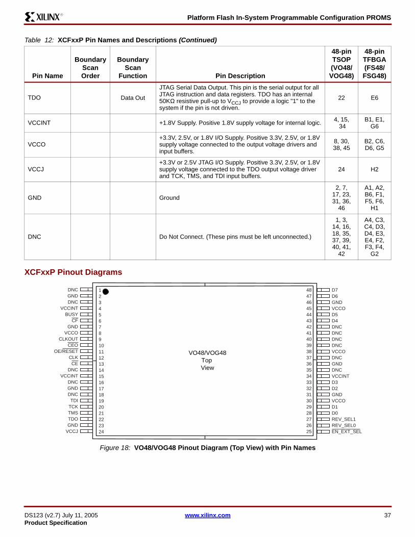
Platform Flash In-System Programmable Configuration PROMS
DS123 (v27) July 11 2005 wwwxilinxcom 37Product Specification
R
XCFxxP Pinout Diagrams
Figure 18 VO48VOG48 Pinout Diagram (Top View) with Pin Names
TDO Data Out
JTAG Serial Data Output This pin is the serial output for all JTAG instruction and data registers TDO has an internal 50KΩ resistive pull-up to VCCJ to provide a logic 1 to the system if the pin is not driven
22 E6
VCCINT +18V Supply Positive 18V supply voltage for internal logic 4 15 34
B1 E1 G6
VCCO+33V 25V or 18V IO Supply Positive 33V 25V or 18V supply voltage connected to the output voltage drivers and input buffers
8 30 38 45
B2 C6 D6 G5
VCCJ+33V or 25V JTAG IO Supply Positive 33V 25V or 18V supply voltage connected to the TDO output voltage driver and TCK TMS and TDI input buffers
24 H2
GND Ground2 7
17 23 31 36
46
A1 A2 B6 F1 F5 F6
H1
DNC Do Not Connect (These pins must be left unconnected)
1 3 14 16 18 35 37 39 40 41
42
A4 C3 C4 D3 D4 E3 E4 F2 F3 F4
G2
Table 12 XCFxxP Pin Names and Descriptions (Continued)
Pin Name
Boundary Scan Order
Boundary Scan
Function Pin Description
48-pin TSOP (VO48VOG48)
48-pin TFBGA (FS48FSG48)
123456789101112131415161718192021222324
484746454443424140393837363534333231302928272625
VO48VOG48Top View
DNCGNDDNC
VCCINTBUSY
CFGND
VCCOCLKOUT
CEOOERESET
CLKCE
DNCVCCINT
DNCGNDDNCTDI
TCKTMSTDOGND
D7D6GNDVCCOD5D4DNCDNCDNCDNCVCCODNCGNDDNCVCCINTD3D2GNDVCCOD1D0REV_SEL1REV_SEL0EN_EXT_SELVCCJ
Platform Flash In-System Programmable Configuration PROMS
DS123 (v27) July 11 2005 wwwxilinxcom 38Product Specification
R
Table 13 FS48FSG48 Pin NumberName ReferencePin
Number Pin NamePin
Number Pin NameA1 GND E1 VCCINT
A2 GND E2 TMS
A3 OERESET E3 DNC
A4 DNC E4 DNC
A5 D6 E5 D2
A6 D7 E6 TDO
B1 VCCINT F1 GND
B2 VCCO F2 DNC
B3 CLK F3 DNC
B4 CE F4 DNC
B5 D5 F5 GND
B6 GND F6 GND
C1 BUSY G1 TDI
C2 CLKOUT G2 DNC
C3 DNC G3 REV_SEL0
C4 DNC G4 REV_SEL1
C5 D4 G5 VCCO
C6 VCCO G6 VCCINT
D1 CF H1 GND
D2 CEO H2 VCCJ
D3 DNC H3 TCK
D4 DNC H4 EN_EXT_SEL
D5 D3 H5 D1
D6 VCCO H6 D0
Table 13 FS48FSG48 Pin NumberName ReferencePin
Number Pin NamePin
Number Pin Name
1 2 3 4 5 6
ds121_01_071604
A
B
C
D
E
F
G
H
FS48FSG48Top View
Platform Flash In-System Programmable Configuration PROMS
DS123 (v27) July 11 2005 wwwxilinxcom 39Product Specification
R
Ordering Information
Valid Ordering Combinations
Marking Information
XCF01SVO20 C XCF08PVO48 C XCF08PFS48 C XCF01SVOG20 C XCF08PVOG48 C XCF08PFSG48 C
XCF02SVO20 C XCF16PVO48 C XCF16PFS48 C XCF02SVOG20 C XCF16PVOG48 C XCF16PFSG48 C
XCF04SVO20 C XCF32PVO48 C XCF32PFS48 C XCF04SVOG20 C XCF32PVOG48 C XCF32PFSG48 C
XCF04S VO20 C
Operating RangeProcessingC = (TA = ndash40degC to +85degC)Package Type
VO20 = 20-pin TSSOP PackageVOG20 = 20-pin TSSOP Package Pb-free
Device NumberXCF01SXCF02SXCF04S
XCF32P FS48 C
Operating RangeProcessingC = (TA = ndash40degC to +85degC)Package Type
VO48 = 48-pin TSOP PackageVOG48 = 48-pin TSOP Package Pb-freeFS48 = 48-pin TFBGA PackageFSG48 = 48-pin TFBGA Package Pb-free
Device NumberXCF08PXCF16PXCF32P
XCF04S-V
Operating RangeProcessingC = (TA = ndash40degC to +85degC)Package Type
V = 20-pin TSSOP Package (VO20)VG = 20-pin TSSOP Package Pb-free (VOG20)VO48 = 48-pin TSOP Package (VO48)VOG48 = 48-pin TSOP Package Pb-free (VOG48)F48 = 48-pin TFBGA Package (FS48)FG48 = 48-pin TFBGA Package Pb-free (FSG48)
Device NumberXCF01SXCF02SXCF04SXCF08PXCF16PXCF32P
huffman
XCF08PFS48 C
huffman
XCF08P
huffman
XCF08P
Platform Flash In-System Programmable Configuration PROMS
DS123 (v27) July 11 2005 wwwxilinxcom 40Product Specification
R
Revision HistoryThe following table shows the revision history for this document
Date Version Revision
042903 10 Xilinx Initial Release
060303 11 Made edits to all pages
110503 20 Major revision
111803 21 Pinout corrections as followsbull Table 12
- For VO48 package removed 38 from VCCINT and added it to VCCO- For FS48 package removed pin D6 from VCCINT and added it to VCCO
bull Table 13 (FS48 package) - For pin D6 changed name from VCCINT to VCCO- For pin A4 changed name from GND to DNC
bull Figure 18 (VO48 package) For pin 38 changed name from VCCINT to VCCO
121503 22 bull Added specification (47kΩ) for recommended pull-up resistor on OERESET pin to section Reset and Power-On Reset Activation page 22
bull Added paragraph to section Standby Mode page 22 concerning use of a pull-up resistor andor buffer on the DONE pin
050704 23 bull Section Features page 1 Added package styles and 33 MHz configuration speed limit to itemized features
bull Section Description page 1 and following Added state conditions for CF and BUSY to the descriptive text
bull Table 2 page 3 Updated Virtex-II configuration bitstream sizesbull Section Design Revisioning page 9 Rewrittenbull Section PROM to FPGA Configuration Mode and Connections Summary
page 10 and following five instances Added instruction to tie CF High if it is not tied to the FPGArsquos PROG_B (PROGRAM) input
bull Figure 8 page 14 through Figure 15 page 21 Added footnote indicating the directionality of the CF pin in each configuration
bull Section IO Input Voltage Tolerance and Power Sequencing page 22 Rewrittenbull Table 10 page 23 Added CF column to truth table and added an additional row to
document the Low state of CFbull Section Absolute Maximum Ratings page 24 Revised VIN and VTS for rsquoPrsquo
devices bull Section Supply Voltage Requirements for Power-On Reset and Power-Down
page 24- Revised footnote callout number on TOER from Footnote (4) to Footnote (3)- Added Footnote (2) callout to TVCC
bull Section Recommended Operating Conditions page 25 - Added Typical (Typ) parameter columns and parameters for VCCINT and
VCCOVCCJ- Added 15V operation parameter row to VIL and VIH rsquoPrsquo devices- Revised VIH Min 25V operation from 20V to 17V- Added parameter row TIN and Max parameters
bull (Continued on next page)
Platform Flash In-System Programmable Configuration PROMS
DS123 (v27) July 11 2005 wwwxilinxcom 41Product Specification
R
050704(contrsquod)
23(contrsquod)
bull Section DC Characteristics Over Operating Conditions page 26 - Added parameter row and parameters for parallel configuration mode rsquoPrsquo
devices to ICCO- Added Footnote (1) and Footnote (2) with callouts in the Test Conditions column
for ICCJ ICCINTS ICCOS and ICCJS to define active and standby mode requirements
bull Section AC Characteristics Over Operating Conditions page 28 - Corrected description for second TCAC parameter line to show parameters for
18V VCCO- Revised Footnote (7) to indicate VCCO = 33V- Applied Footnote (7) to second TCYC parameter line
bull Section AC Characteristics Over Operating Conditions When Cascading page 32 Revised Footnote (5)TCYC Min and TCAC Min formulas
bull Table 12 page 35 - Added additional state conditions to CLK description- Added function of resetting the internal address counter to CF description
072004 24 bull Added Pb-free package options VOG20 FSG48 and VOG48bull Figure 8 page 14 and Figure 9 page 15 Corrected connection name for FPGA
DOUT (OPTIONAL Daisy-chained Slave FPGAs with different configurations) from DOUT to DIN
bull Section Absolute Maximum Ratings page 24 Removed parameter TSOL from table (TSOL information can be found in Package User Guide)
bull Table 2 page 3 Removed reference to XC2VP125 FPGA
101804 25 bull Table 1 page 1 Broke out VCCO VCCJ into two separate columnsbull Table 7 page 7 Added clarification of ID code die revision bitsbull Table 8 page 8 Deleted TCKMIN2 (bypass mode) and renamed TCKMIN1 to TCKMINbull Table Recommended Operating Conditions page 25 Separated VCCO and VCCJ
parametersbull Table DC Characteristics Over Operating Conditions page 26
- Added most parameter values for XCF08P XCF16P XCF32P devices- Added Footnote (1) to ICCO specifying no-load conditions
bull Table AC Characteristics Over Operating Conditions page 28 - Added most parameter values for XCF08P XCF16P XCF32P devices- Expanded Footnote (1) to include XCF08P XCF16P XCF32P devices- Added Footnote (8) through (11) relating to CLKOUT conditions for various
parameters- Added rows to TCYC specifying parameters for parallel mode- Added rows specifying parameters with decompression for TCLKO TCOH TFF
TSF- Added TDDC (setup time with decompression)
bull Table AC Characteristics Over Operating Conditions When Cascading page 32 - Added most parameter values for XCF08P XCF16P XCF32P devices- Separated Footnote (5) into Footnotes (5) and (6) to specify different
derivations of TCYC depending on whether dual-purpose configuration pins persist as configuration pins or become general IO pins after configuration
huffman
XCF08P
huffman
XCF08P
huffman
XCF08P
huffman
XCF08P
Platform Flash In-System Programmable Configuration PROMS
DS123 (v27) July 11 2005 wwwxilinxcom 42Product Specification
R
031405 26 bull Added Virtex-4 LXFXSX configuration data to Table 2 bull Corrected Virtex-II configuration data in Table 2bull Corrected Virtex-II Pro configuration data in Table 2bull Added Spartan-3L configuration data to Table 2bull Added Spartan-3E configuration data to Table 2bull Paragraph added to FPGA Master SelectMAP (Parallel) Mode (1) page 11bull Changes to DC Characteristics
- TOER changed page 26- IOL changed for VOL page 26- VCCO added to test conditions for IIL IILP IIHPand IIH page 26 Values modified
for IILP and IIHPbull Changes to AC Characteristics
- TLC and THC modified for 18V page 29- New rows added for TCEC and TOEC page 29
bull Minor changes to grammar and punctuationbull Add explanation of Preliminary to DC and AC Electrical Characteristics
071105 27 bull Move from Preliminary to Product Specificationbull Corrections to Virtex-4 configuration bitstream valuesbull Minor changes to figures 9 14 15 and 18bull Change to Internal Oscillator description page 8bull Change to CLKOUT description page 8
- Platform Flash In-System Programmable Configuration PROMS
-
- Features
- Description
- Programming
-
- In-System Programming
-
- OERESET
-
- External Programming
- Reliability and Endurance
-
- Design Security
-
- Read Protection
- Write Protection
-
- IEEE 11491 Boundary-Scan (JTAG)
-
- Instruction Register
-
- XCFxxS Instruction Register (8 bits wide)
- XCFxxP Instruction Register (16 bits wide)
-
- Boundary Scan Register
- Identification Registers
-
- IDCODE Register
- USERCODE Register
- Customer Code Register
-
- Platform Flash PROM TAP Characteristics
-
- TAP Timing
- TAP AC Parameters
-
- Additional Features for the XCFxxP
-
- Internal Oscillator
- CLKOUT
- Decompression
- Design Revisioning
-
- PROM to FPGA Configuration Mode and Connections Summary
-
- FPGA Master Serial Mode
- FPGA Slave Serial Mode
- Serial Daisy Chain
- FPGA Master SelectMAP (Parallel) Mode
- FPGA Slave SelectMAP (Parallel) Mode
- FPGA SelectMAP (Parallel) Device Chaining
- Cascading Configuration PROMs
- Initiating FPGA Configuration
-
- Configuration PROM to FPGA Device Interface Connection Diagrams
- Reset and Power-On Reset Activation
- IO Input Voltage Tolerance and Power Sequencing
- Standby Mode
- DC Electrical Characteristics
- AC Electrical Characteristics
-
- Absolute Maximum Ratings
- Supply Voltage Requirements for Power-On Reset and Power-Down
- Recommended Operating Conditions
- Quality and Reliability Characteristics
- DC Characteristics Over Operating Conditions
- AC Characteristics Over Operating Conditions
- AC Characteristics Over Operating Conditions When Cascading
-
- Pinouts and Pin Descriptions
-
- XCFxxS Pinouts and Pin Descriptions
- XCFxxS Pinout Diagram
- XCFxxP Pinouts and Pin Descriptions
- XCFxxP Pinout Diagrams
-
- Ordering Information
- Valid Ordering Combinations
- Marking Information
- Revision History
-
Platform Flash In-System Programmable Configuration PROMS
DS123 (v27) July 11 2005 wwwxilinxcom 38Product Specification
R
Table 13 FS48FSG48 Pin NumberName ReferencePin
Number Pin NamePin
Number Pin NameA1 GND E1 VCCINT
A2 GND E2 TMS
A3 OERESET E3 DNC
A4 DNC E4 DNC
A5 D6 E5 D2
A6 D7 E6 TDO
B1 VCCINT F1 GND
B2 VCCO F2 DNC
B3 CLK F3 DNC
B4 CE F4 DNC
B5 D5 F5 GND
B6 GND F6 GND
C1 BUSY G1 TDI
C2 CLKOUT G2 DNC
C3 DNC G3 REV_SEL0
C4 DNC G4 REV_SEL1
C5 D4 G5 VCCO
C6 VCCO G6 VCCINT
D1 CF H1 GND
D2 CEO H2 VCCJ
D3 DNC H3 TCK
D4 DNC H4 EN_EXT_SEL
D5 D3 H5 D1
D6 VCCO H6 D0
Table 13 FS48FSG48 Pin NumberName ReferencePin
Number Pin NamePin
Number Pin Name
1 2 3 4 5 6
ds121_01_071604
A
B
C
D
E
F
G
H
FS48FSG48Top View
Platform Flash In-System Programmable Configuration PROMS
DS123 (v27) July 11 2005 wwwxilinxcom 39Product Specification
R
Ordering Information
Valid Ordering Combinations
Marking Information
XCF01SVO20 C XCF08PVO48 C XCF08PFS48 C XCF01SVOG20 C XCF08PVOG48 C XCF08PFSG48 C
XCF02SVO20 C XCF16PVO48 C XCF16PFS48 C XCF02SVOG20 C XCF16PVOG48 C XCF16PFSG48 C
XCF04SVO20 C XCF32PVO48 C XCF32PFS48 C XCF04SVOG20 C XCF32PVOG48 C XCF32PFSG48 C
XCF04S VO20 C
Operating RangeProcessingC = (TA = ndash40degC to +85degC)Package Type
VO20 = 20-pin TSSOP PackageVOG20 = 20-pin TSSOP Package Pb-free
Device NumberXCF01SXCF02SXCF04S
XCF32P FS48 C
Operating RangeProcessingC = (TA = ndash40degC to +85degC)Package Type
VO48 = 48-pin TSOP PackageVOG48 = 48-pin TSOP Package Pb-freeFS48 = 48-pin TFBGA PackageFSG48 = 48-pin TFBGA Package Pb-free
Device NumberXCF08PXCF16PXCF32P
XCF04S-V
Operating RangeProcessingC = (TA = ndash40degC to +85degC)Package Type
V = 20-pin TSSOP Package (VO20)VG = 20-pin TSSOP Package Pb-free (VOG20)VO48 = 48-pin TSOP Package (VO48)VOG48 = 48-pin TSOP Package Pb-free (VOG48)F48 = 48-pin TFBGA Package (FS48)FG48 = 48-pin TFBGA Package Pb-free (FSG48)
Device NumberXCF01SXCF02SXCF04SXCF08PXCF16PXCF32P
huffman
XCF08PFS48 C
huffman
XCF08P
huffman
XCF08P
Platform Flash In-System Programmable Configuration PROMS
DS123 (v27) July 11 2005 wwwxilinxcom 40Product Specification
R
Revision HistoryThe following table shows the revision history for this document
Date Version Revision
042903 10 Xilinx Initial Release
060303 11 Made edits to all pages
110503 20 Major revision
111803 21 Pinout corrections as followsbull Table 12
- For VO48 package removed 38 from VCCINT and added it to VCCO- For FS48 package removed pin D6 from VCCINT and added it to VCCO
bull Table 13 (FS48 package) - For pin D6 changed name from VCCINT to VCCO- For pin A4 changed name from GND to DNC
bull Figure 18 (VO48 package) For pin 38 changed name from VCCINT to VCCO
121503 22 bull Added specification (47kΩ) for recommended pull-up resistor on OERESET pin to section Reset and Power-On Reset Activation page 22
bull Added paragraph to section Standby Mode page 22 concerning use of a pull-up resistor andor buffer on the DONE pin
050704 23 bull Section Features page 1 Added package styles and 33 MHz configuration speed limit to itemized features
bull Section Description page 1 and following Added state conditions for CF and BUSY to the descriptive text
bull Table 2 page 3 Updated Virtex-II configuration bitstream sizesbull Section Design Revisioning page 9 Rewrittenbull Section PROM to FPGA Configuration Mode and Connections Summary
page 10 and following five instances Added instruction to tie CF High if it is not tied to the FPGArsquos PROG_B (PROGRAM) input
bull Figure 8 page 14 through Figure 15 page 21 Added footnote indicating the directionality of the CF pin in each configuration
bull Section IO Input Voltage Tolerance and Power Sequencing page 22 Rewrittenbull Table 10 page 23 Added CF column to truth table and added an additional row to
document the Low state of CFbull Section Absolute Maximum Ratings page 24 Revised VIN and VTS for rsquoPrsquo
devices bull Section Supply Voltage Requirements for Power-On Reset and Power-Down
page 24- Revised footnote callout number on TOER from Footnote (4) to Footnote (3)- Added Footnote (2) callout to TVCC
bull Section Recommended Operating Conditions page 25 - Added Typical (Typ) parameter columns and parameters for VCCINT and
VCCOVCCJ- Added 15V operation parameter row to VIL and VIH rsquoPrsquo devices- Revised VIH Min 25V operation from 20V to 17V- Added parameter row TIN and Max parameters
bull (Continued on next page)
Platform Flash In-System Programmable Configuration PROMS
DS123 (v27) July 11 2005 wwwxilinxcom 41Product Specification
R
050704(contrsquod)
23(contrsquod)
bull Section DC Characteristics Over Operating Conditions page 26 - Added parameter row and parameters for parallel configuration mode rsquoPrsquo
devices to ICCO- Added Footnote (1) and Footnote (2) with callouts in the Test Conditions column
for ICCJ ICCINTS ICCOS and ICCJS to define active and standby mode requirements
bull Section AC Characteristics Over Operating Conditions page 28 - Corrected description for second TCAC parameter line to show parameters for
18V VCCO- Revised Footnote (7) to indicate VCCO = 33V- Applied Footnote (7) to second TCYC parameter line
bull Section AC Characteristics Over Operating Conditions When Cascading page 32 Revised Footnote (5)TCYC Min and TCAC Min formulas
bull Table 12 page 35 - Added additional state conditions to CLK description- Added function of resetting the internal address counter to CF description
072004 24 bull Added Pb-free package options VOG20 FSG48 and VOG48bull Figure 8 page 14 and Figure 9 page 15 Corrected connection name for FPGA
DOUT (OPTIONAL Daisy-chained Slave FPGAs with different configurations) from DOUT to DIN
bull Section Absolute Maximum Ratings page 24 Removed parameter TSOL from table (TSOL information can be found in Package User Guide)
bull Table 2 page 3 Removed reference to XC2VP125 FPGA
101804 25 bull Table 1 page 1 Broke out VCCO VCCJ into two separate columnsbull Table 7 page 7 Added clarification of ID code die revision bitsbull Table 8 page 8 Deleted TCKMIN2 (bypass mode) and renamed TCKMIN1 to TCKMINbull Table Recommended Operating Conditions page 25 Separated VCCO and VCCJ
parametersbull Table DC Characteristics Over Operating Conditions page 26
- Added most parameter values for XCF08P XCF16P XCF32P devices- Added Footnote (1) to ICCO specifying no-load conditions
bull Table AC Characteristics Over Operating Conditions page 28 - Added most parameter values for XCF08P XCF16P XCF32P devices- Expanded Footnote (1) to include XCF08P XCF16P XCF32P devices- Added Footnote (8) through (11) relating to CLKOUT conditions for various
parameters- Added rows to TCYC specifying parameters for parallel mode- Added rows specifying parameters with decompression for TCLKO TCOH TFF
TSF- Added TDDC (setup time with decompression)
bull Table AC Characteristics Over Operating Conditions When Cascading page 32 - Added most parameter values for XCF08P XCF16P XCF32P devices- Separated Footnote (5) into Footnotes (5) and (6) to specify different
derivations of TCYC depending on whether dual-purpose configuration pins persist as configuration pins or become general IO pins after configuration
huffman
XCF08P
huffman
XCF08P
huffman
XCF08P
huffman
XCF08P
Platform Flash In-System Programmable Configuration PROMS
DS123 (v27) July 11 2005 wwwxilinxcom 42Product Specification
R
031405 26 bull Added Virtex-4 LXFXSX configuration data to Table 2 bull Corrected Virtex-II configuration data in Table 2bull Corrected Virtex-II Pro configuration data in Table 2bull Added Spartan-3L configuration data to Table 2bull Added Spartan-3E configuration data to Table 2bull Paragraph added to FPGA Master SelectMAP (Parallel) Mode (1) page 11bull Changes to DC Characteristics
- TOER changed page 26- IOL changed for VOL page 26- VCCO added to test conditions for IIL IILP IIHPand IIH page 26 Values modified
for IILP and IIHPbull Changes to AC Characteristics
- TLC and THC modified for 18V page 29- New rows added for TCEC and TOEC page 29
bull Minor changes to grammar and punctuationbull Add explanation of Preliminary to DC and AC Electrical Characteristics
071105 27 bull Move from Preliminary to Product Specificationbull Corrections to Virtex-4 configuration bitstream valuesbull Minor changes to figures 9 14 15 and 18bull Change to Internal Oscillator description page 8bull Change to CLKOUT description page 8
- Platform Flash In-System Programmable Configuration PROMS
-
- Features
- Description
- Programming
-
- In-System Programming
-
- OERESET
-
- External Programming
- Reliability and Endurance
-
- Design Security
-
- Read Protection
- Write Protection
-
- IEEE 11491 Boundary-Scan (JTAG)
-
- Instruction Register
-
- XCFxxS Instruction Register (8 bits wide)
- XCFxxP Instruction Register (16 bits wide)
-
- Boundary Scan Register
- Identification Registers
-
- IDCODE Register
- USERCODE Register
- Customer Code Register
-
- Platform Flash PROM TAP Characteristics
-
- TAP Timing
- TAP AC Parameters
-
- Additional Features for the XCFxxP
-
- Internal Oscillator
- CLKOUT
- Decompression
- Design Revisioning
-
- PROM to FPGA Configuration Mode and Connections Summary
-
- FPGA Master Serial Mode
- FPGA Slave Serial Mode
- Serial Daisy Chain
- FPGA Master SelectMAP (Parallel) Mode
- FPGA Slave SelectMAP (Parallel) Mode
- FPGA SelectMAP (Parallel) Device Chaining
- Cascading Configuration PROMs
- Initiating FPGA Configuration
-
- Configuration PROM to FPGA Device Interface Connection Diagrams
- Reset and Power-On Reset Activation
- IO Input Voltage Tolerance and Power Sequencing
- Standby Mode
- DC Electrical Characteristics
- AC Electrical Characteristics
-
- Absolute Maximum Ratings
- Supply Voltage Requirements for Power-On Reset and Power-Down
- Recommended Operating Conditions
- Quality and Reliability Characteristics
- DC Characteristics Over Operating Conditions
- AC Characteristics Over Operating Conditions
- AC Characteristics Over Operating Conditions When Cascading
-
- Pinouts and Pin Descriptions
-
- XCFxxS Pinouts and Pin Descriptions
- XCFxxS Pinout Diagram
- XCFxxP Pinouts and Pin Descriptions
- XCFxxP Pinout Diagrams
-
- Ordering Information
- Valid Ordering Combinations
- Marking Information
- Revision History
-
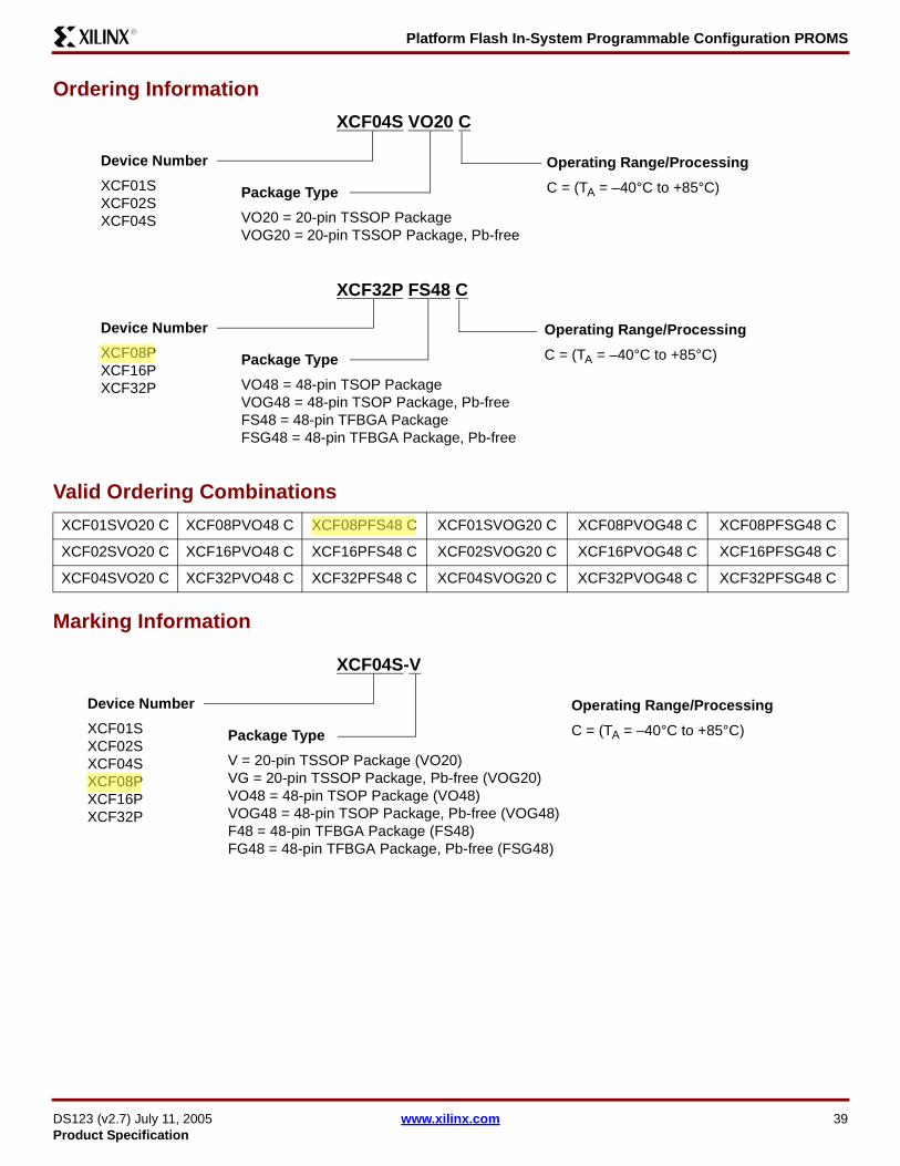
Platform Flash In-System Programmable Configuration PROMS
DS123 (v27) July 11 2005 wwwxilinxcom 39Product Specification
R
Ordering Information
Valid Ordering Combinations
Marking Information
XCF01SVO20 C XCF08PVO48 C XCF08PFS48 C XCF01SVOG20 C XCF08PVOG48 C XCF08PFSG48 C
XCF02SVO20 C XCF16PVO48 C XCF16PFS48 C XCF02SVOG20 C XCF16PVOG48 C XCF16PFSG48 C
XCF04SVO20 C XCF32PVO48 C XCF32PFS48 C XCF04SVOG20 C XCF32PVOG48 C XCF32PFSG48 C
XCF04S VO20 C
Operating RangeProcessingC = (TA = ndash40degC to +85degC)Package Type
VO20 = 20-pin TSSOP PackageVOG20 = 20-pin TSSOP Package Pb-free
Device NumberXCF01SXCF02SXCF04S
XCF32P FS48 C
Operating RangeProcessingC = (TA = ndash40degC to +85degC)Package Type
VO48 = 48-pin TSOP PackageVOG48 = 48-pin TSOP Package Pb-freeFS48 = 48-pin TFBGA PackageFSG48 = 48-pin TFBGA Package Pb-free
Device NumberXCF08PXCF16PXCF32P
XCF04S-V
Operating RangeProcessingC = (TA = ndash40degC to +85degC)Package Type
V = 20-pin TSSOP Package (VO20)VG = 20-pin TSSOP Package Pb-free (VOG20)VO48 = 48-pin TSOP Package (VO48)VOG48 = 48-pin TSOP Package Pb-free (VOG48)F48 = 48-pin TFBGA Package (FS48)FG48 = 48-pin TFBGA Package Pb-free (FSG48)
Device NumberXCF01SXCF02SXCF04SXCF08PXCF16PXCF32P
huffman
XCF08PFS48 C
huffman
XCF08P
huffman
XCF08P
Platform Flash In-System Programmable Configuration PROMS
DS123 (v27) July 11 2005 wwwxilinxcom 40Product Specification
R
Revision HistoryThe following table shows the revision history for this document
Date Version Revision
042903 10 Xilinx Initial Release
060303 11 Made edits to all pages
110503 20 Major revision
111803 21 Pinout corrections as followsbull Table 12
- For VO48 package removed 38 from VCCINT and added it to VCCO- For FS48 package removed pin D6 from VCCINT and added it to VCCO
bull Table 13 (FS48 package) - For pin D6 changed name from VCCINT to VCCO- For pin A4 changed name from GND to DNC
bull Figure 18 (VO48 package) For pin 38 changed name from VCCINT to VCCO
121503 22 bull Added specification (47kΩ) for recommended pull-up resistor on OERESET pin to section Reset and Power-On Reset Activation page 22
bull Added paragraph to section Standby Mode page 22 concerning use of a pull-up resistor andor buffer on the DONE pin
050704 23 bull Section Features page 1 Added package styles and 33 MHz configuration speed limit to itemized features
bull Section Description page 1 and following Added state conditions for CF and BUSY to the descriptive text
bull Table 2 page 3 Updated Virtex-II configuration bitstream sizesbull Section Design Revisioning page 9 Rewrittenbull Section PROM to FPGA Configuration Mode and Connections Summary
page 10 and following five instances Added instruction to tie CF High if it is not tied to the FPGArsquos PROG_B (PROGRAM) input
bull Figure 8 page 14 through Figure 15 page 21 Added footnote indicating the directionality of the CF pin in each configuration
bull Section IO Input Voltage Tolerance and Power Sequencing page 22 Rewrittenbull Table 10 page 23 Added CF column to truth table and added an additional row to
document the Low state of CFbull Section Absolute Maximum Ratings page 24 Revised VIN and VTS for rsquoPrsquo
devices bull Section Supply Voltage Requirements for Power-On Reset and Power-Down
page 24- Revised footnote callout number on TOER from Footnote (4) to Footnote (3)- Added Footnote (2) callout to TVCC
bull Section Recommended Operating Conditions page 25 - Added Typical (Typ) parameter columns and parameters for VCCINT and
VCCOVCCJ- Added 15V operation parameter row to VIL and VIH rsquoPrsquo devices- Revised VIH Min 25V operation from 20V to 17V- Added parameter row TIN and Max parameters
bull (Continued on next page)
Platform Flash In-System Programmable Configuration PROMS
DS123 (v27) July 11 2005 wwwxilinxcom 41Product Specification
R
050704(contrsquod)
23(contrsquod)
bull Section DC Characteristics Over Operating Conditions page 26 - Added parameter row and parameters for parallel configuration mode rsquoPrsquo
devices to ICCO- Added Footnote (1) and Footnote (2) with callouts in the Test Conditions column
for ICCJ ICCINTS ICCOS and ICCJS to define active and standby mode requirements
bull Section AC Characteristics Over Operating Conditions page 28 - Corrected description for second TCAC parameter line to show parameters for
18V VCCO- Revised Footnote (7) to indicate VCCO = 33V- Applied Footnote (7) to second TCYC parameter line
bull Section AC Characteristics Over Operating Conditions When Cascading page 32 Revised Footnote (5)TCYC Min and TCAC Min formulas
bull Table 12 page 35 - Added additional state conditions to CLK description- Added function of resetting the internal address counter to CF description
072004 24 bull Added Pb-free package options VOG20 FSG48 and VOG48bull Figure 8 page 14 and Figure 9 page 15 Corrected connection name for FPGA
DOUT (OPTIONAL Daisy-chained Slave FPGAs with different configurations) from DOUT to DIN
bull Section Absolute Maximum Ratings page 24 Removed parameter TSOL from table (TSOL information can be found in Package User Guide)
bull Table 2 page 3 Removed reference to XC2VP125 FPGA
101804 25 bull Table 1 page 1 Broke out VCCO VCCJ into two separate columnsbull Table 7 page 7 Added clarification of ID code die revision bitsbull Table 8 page 8 Deleted TCKMIN2 (bypass mode) and renamed TCKMIN1 to TCKMINbull Table Recommended Operating Conditions page 25 Separated VCCO and VCCJ
parametersbull Table DC Characteristics Over Operating Conditions page 26
- Added most parameter values for XCF08P XCF16P XCF32P devices- Added Footnote (1) to ICCO specifying no-load conditions
bull Table AC Characteristics Over Operating Conditions page 28 - Added most parameter values for XCF08P XCF16P XCF32P devices- Expanded Footnote (1) to include XCF08P XCF16P XCF32P devices- Added Footnote (8) through (11) relating to CLKOUT conditions for various
parameters- Added rows to TCYC specifying parameters for parallel mode- Added rows specifying parameters with decompression for TCLKO TCOH TFF
TSF- Added TDDC (setup time with decompression)
bull Table AC Characteristics Over Operating Conditions When Cascading page 32 - Added most parameter values for XCF08P XCF16P XCF32P devices- Separated Footnote (5) into Footnotes (5) and (6) to specify different
derivations of TCYC depending on whether dual-purpose configuration pins persist as configuration pins or become general IO pins after configuration
huffman
XCF08P
huffman
XCF08P
huffman
XCF08P
huffman
XCF08P
Platform Flash In-System Programmable Configuration PROMS
DS123 (v27) July 11 2005 wwwxilinxcom 42Product Specification
R
031405 26 bull Added Virtex-4 LXFXSX configuration data to Table 2 bull Corrected Virtex-II configuration data in Table 2bull Corrected Virtex-II Pro configuration data in Table 2bull Added Spartan-3L configuration data to Table 2bull Added Spartan-3E configuration data to Table 2bull Paragraph added to FPGA Master SelectMAP (Parallel) Mode (1) page 11bull Changes to DC Characteristics
- TOER changed page 26- IOL changed for VOL page 26- VCCO added to test conditions for IIL IILP IIHPand IIH page 26 Values modified
for IILP and IIHPbull Changes to AC Characteristics
- TLC and THC modified for 18V page 29- New rows added for TCEC and TOEC page 29
bull Minor changes to grammar and punctuationbull Add explanation of Preliminary to DC and AC Electrical Characteristics
071105 27 bull Move from Preliminary to Product Specificationbull Corrections to Virtex-4 configuration bitstream valuesbull Minor changes to figures 9 14 15 and 18bull Change to Internal Oscillator description page 8bull Change to CLKOUT description page 8
- Platform Flash In-System Programmable Configuration PROMS
-
- Features
- Description
- Programming
-
- In-System Programming
-
- OERESET
-
- External Programming
- Reliability and Endurance
-
- Design Security
-
- Read Protection
- Write Protection
-
- IEEE 11491 Boundary-Scan (JTAG)
-
- Instruction Register
-
- XCFxxS Instruction Register (8 bits wide)
- XCFxxP Instruction Register (16 bits wide)
-
- Boundary Scan Register
- Identification Registers
-
- IDCODE Register
- USERCODE Register
- Customer Code Register
-
- Platform Flash PROM TAP Characteristics
-
- TAP Timing
- TAP AC Parameters
-
- Additional Features for the XCFxxP
-
- Internal Oscillator
- CLKOUT
- Decompression
- Design Revisioning
-
- PROM to FPGA Configuration Mode and Connections Summary
-
- FPGA Master Serial Mode
- FPGA Slave Serial Mode
- Serial Daisy Chain
- FPGA Master SelectMAP (Parallel) Mode
- FPGA Slave SelectMAP (Parallel) Mode
- FPGA SelectMAP (Parallel) Device Chaining
- Cascading Configuration PROMs
- Initiating FPGA Configuration
-
- Configuration PROM to FPGA Device Interface Connection Diagrams
- Reset and Power-On Reset Activation
- IO Input Voltage Tolerance and Power Sequencing
- Standby Mode
- DC Electrical Characteristics
- AC Electrical Characteristics
-
- Absolute Maximum Ratings
- Supply Voltage Requirements for Power-On Reset and Power-Down
- Recommended Operating Conditions
- Quality and Reliability Characteristics
- DC Characteristics Over Operating Conditions
- AC Characteristics Over Operating Conditions
- AC Characteristics Over Operating Conditions When Cascading
-
- Pinouts and Pin Descriptions
-
- XCFxxS Pinouts and Pin Descriptions
- XCFxxS Pinout Diagram
- XCFxxP Pinouts and Pin Descriptions
- XCFxxP Pinout Diagrams
-
- Ordering Information
- Valid Ordering Combinations
- Marking Information
- Revision History
-
Platform Flash In-System Programmable Configuration PROMS
DS123 (v27) July 11 2005 wwwxilinxcom 41Product Specification
R
050704(contrsquod)
23(contrsquod)
bull Section DC Characteristics Over Operating Conditions page 26 - Added parameter row and parameters for parallel configuration mode rsquoPrsquo
devices to ICCO- Added Footnote (1) and Footnote (2) with callouts in the Test Conditions column
for ICCJ ICCINTS ICCOS and ICCJS to define active and standby mode requirements
bull Section AC Characteristics Over Operating Conditions page 28 - Corrected description for second TCAC parameter line to show parameters for
18V VCCO- Revised Footnote (7) to indicate VCCO = 33V- Applied Footnote (7) to second TCYC parameter line
bull Section AC Characteristics Over Operating Conditions When Cascading page 32 Revised Footnote (5)TCYC Min and TCAC Min formulas
bull Table 12 page 35 - Added additional state conditions to CLK description- Added function of resetting the internal address counter to CF description
072004 24 bull Added Pb-free package options VOG20 FSG48 and VOG48bull Figure 8 page 14 and Figure 9 page 15 Corrected connection name for FPGA
DOUT (OPTIONAL Daisy-chained Slave FPGAs with different configurations) from DOUT to DIN
bull Section Absolute Maximum Ratings page 24 Removed parameter TSOL from table (TSOL information can be found in Package User Guide)
bull Table 2 page 3 Removed reference to XC2VP125 FPGA
101804 25 bull Table 1 page 1 Broke out VCCO VCCJ into two separate columnsbull Table 7 page 7 Added clarification of ID code die revision bitsbull Table 8 page 8 Deleted TCKMIN2 (bypass mode) and renamed TCKMIN1 to TCKMINbull Table Recommended Operating Conditions page 25 Separated VCCO and VCCJ
parametersbull Table DC Characteristics Over Operating Conditions page 26
- Added most parameter values for XCF08P XCF16P XCF32P devices- Added Footnote (1) to ICCO specifying no-load conditions
bull Table AC Characteristics Over Operating Conditions page 28 - Added most parameter values for XCF08P XCF16P XCF32P devices- Expanded Footnote (1) to include XCF08P XCF16P XCF32P devices- Added Footnote (8) through (11) relating to CLKOUT conditions for various
parameters- Added rows to TCYC specifying parameters for parallel mode- Added rows specifying parameters with decompression for TCLKO TCOH TFF
TSF- Added TDDC (setup time with decompression)
bull Table AC Characteristics Over Operating Conditions When Cascading page 32 - Added most parameter values for XCF08P XCF16P XCF32P devices- Separated Footnote (5) into Footnotes (5) and (6) to specify different
derivations of TCYC depending on whether dual-purpose configuration pins persist as configuration pins or become general IO pins after configuration
huffman
XCF08P
huffman
XCF08P
huffman
XCF08P
huffman
XCF08P
Platform Flash In-System Programmable Configuration PROMS
DS123 (v27) July 11 2005 wwwxilinxcom 42Product Specification
R
031405 26 bull Added Virtex-4 LXFXSX configuration data to Table 2 bull Corrected Virtex-II configuration data in Table 2bull Corrected Virtex-II Pro configuration data in Table 2bull Added Spartan-3L configuration data to Table 2bull Added Spartan-3E configuration data to Table 2bull Paragraph added to FPGA Master SelectMAP (Parallel) Mode (1) page 11bull Changes to DC Characteristics
- TOER changed page 26- IOL changed for VOL page 26- VCCO added to test conditions for IIL IILP IIHPand IIH page 26 Values modified
for IILP and IIHPbull Changes to AC Characteristics
- TLC and THC modified for 18V page 29- New rows added for TCEC and TOEC page 29
bull Minor changes to grammar and punctuationbull Add explanation of Preliminary to DC and AC Electrical Characteristics
071105 27 bull Move from Preliminary to Product Specificationbull Corrections to Virtex-4 configuration bitstream valuesbull Minor changes to figures 9 14 15 and 18bull Change to Internal Oscillator description page 8bull Change to CLKOUT description page 8
- Platform Flash In-System Programmable Configuration PROMS
-
- Features
- Description
- Programming
-
- In-System Programming
-
- OERESET
-
- External Programming
- Reliability and Endurance
-
- Design Security
-
- Read Protection
- Write Protection
-
- IEEE 11491 Boundary-Scan (JTAG)
-
- Instruction Register
-
- XCFxxS Instruction Register (8 bits wide)
- XCFxxP Instruction Register (16 bits wide)
-
- Boundary Scan Register
- Identification Registers
-
- IDCODE Register
- USERCODE Register
- Customer Code Register
-
- Platform Flash PROM TAP Characteristics
-
- TAP Timing
- TAP AC Parameters
-
- Additional Features for the XCFxxP
-
- Internal Oscillator
- CLKOUT
- Decompression
- Design Revisioning
-
- PROM to FPGA Configuration Mode and Connections Summary
-
- FPGA Master Serial Mode
- FPGA Slave Serial Mode
- Serial Daisy Chain
- FPGA Master SelectMAP (Parallel) Mode
- FPGA Slave SelectMAP (Parallel) Mode
- FPGA SelectMAP (Parallel) Device Chaining
- Cascading Configuration PROMs
- Initiating FPGA Configuration
-
- Configuration PROM to FPGA Device Interface Connection Diagrams
- Reset and Power-On Reset Activation
- IO Input Voltage Tolerance and Power Sequencing
- Standby Mode
- DC Electrical Characteristics
- AC Electrical Characteristics
-
- Absolute Maximum Ratings
- Supply Voltage Requirements for Power-On Reset and Power-Down
- Recommended Operating Conditions
- Quality and Reliability Characteristics
- DC Characteristics Over Operating Conditions
- AC Characteristics Over Operating Conditions
- AC Characteristics Over Operating Conditions When Cascading
-
- Pinouts and Pin Descriptions
-
- XCFxxS Pinouts and Pin Descriptions
- XCFxxS Pinout Diagram
- XCFxxP Pinouts and Pin Descriptions
- XCFxxP Pinout Diagrams
-
- Ordering Information
- Valid Ordering Combinations
- Marking Information
- Revision History
-