QUIZ: Perform the minimization using K-maps Ladder logic” analysis The minimization in (c) ......
44
QUIZ: Perform the minimization using K-maps
Transcript of QUIZ: Perform the minimization using K-maps Ladder logic” analysis The minimization in (c) ......
QUIZ: Perform the minimization using K-maps

Perform the minimization using K-maps

Chapter 3
Analysis and Design
of Logic Circuits
Copyright © The McGraw-Hill Companies, Inc. Permission required for reproduction or display.
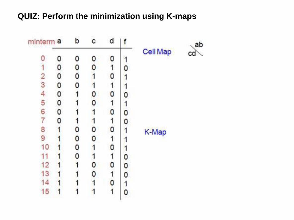
Anatomy of an IC
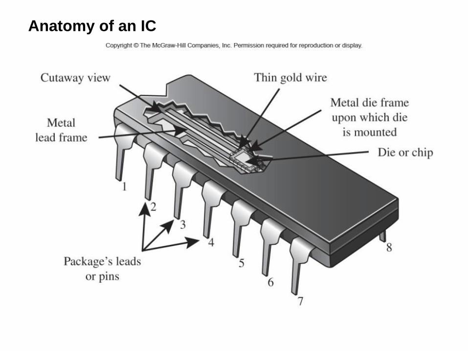
Types of IC packages
PGA (Pin Grid Array) PLCC (Plastic Leaded Chip Carrier)
Flat Package SO (Small Outline) Package
DIP

Latest, coolest package: BGA = Ball Grid Array

Relay logic circuits (Konrad Zuse’s Z2, 1939!)

“Ladder logic” analysis
The minimization in (c) can be done w/any of the methods covered
(Boolean algebra, Venn diagrams, K-maps)

QUIZ
Analyze and minimize this relay circuit
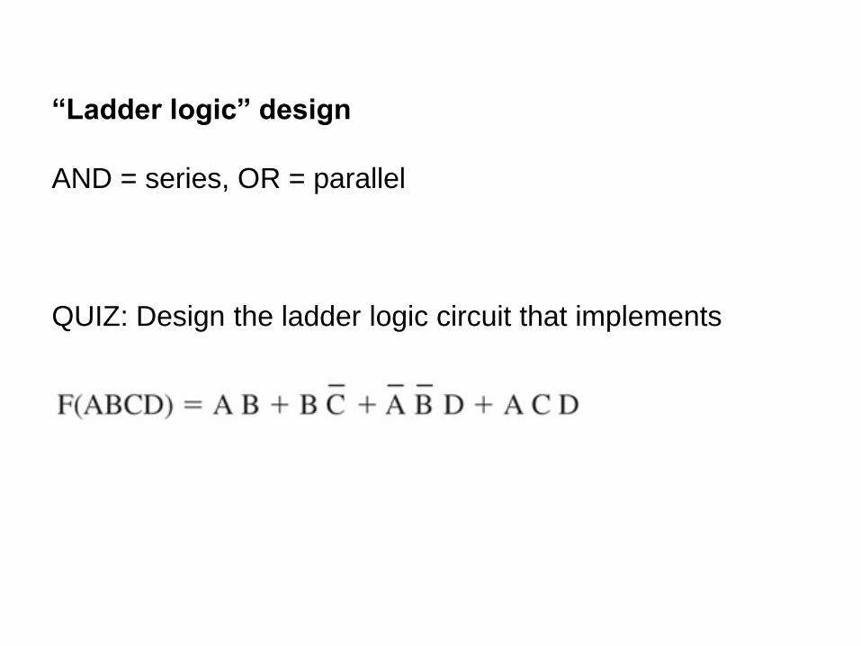
“Ladder logic” design
AND = series, OR = parallel
QUIZ: Design the ladder logic circuit that implements

3.3.2 Analyzing circuits made out of gates
Practice converting between SOP and POS forms using DeMorgan!

3.3.3 Designing circuits with gates: AND-OR
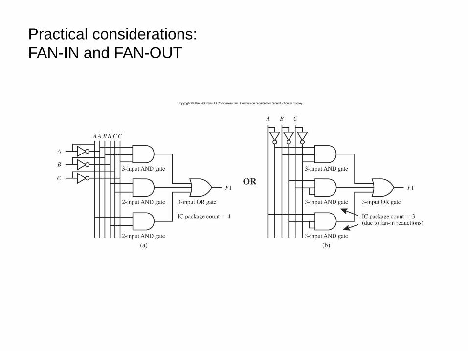
Practical considerations:
FAN-IN and FAN-OUT
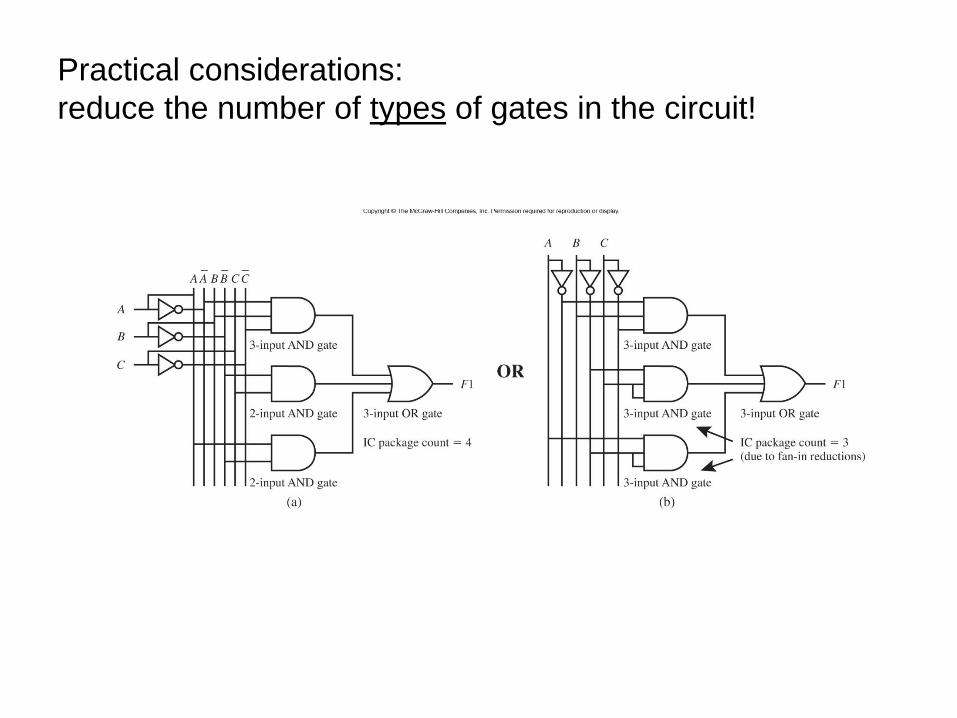
Practical considerations:
reduce the number of types of gates in the circuit!
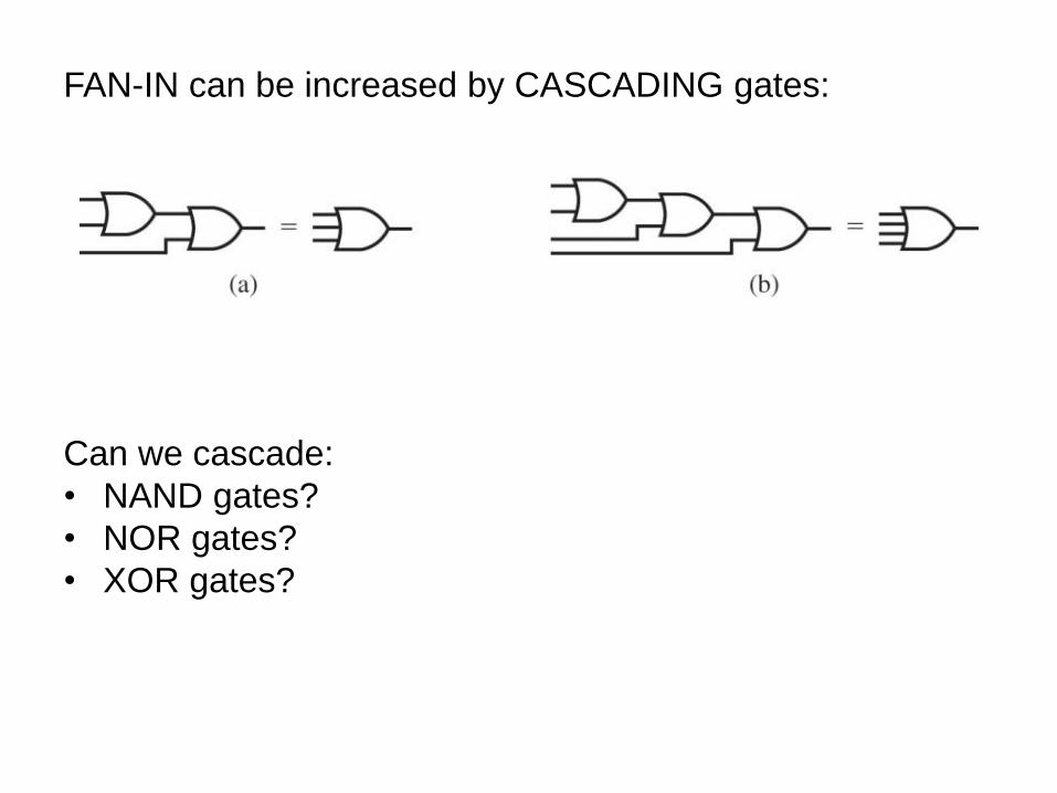
FAN-IN can be increased by CASCADING gates:
Can we cascade:
• NAND gates?
• NOR gates?
• XOR gates?

Designing circuits with gates: OR-AND
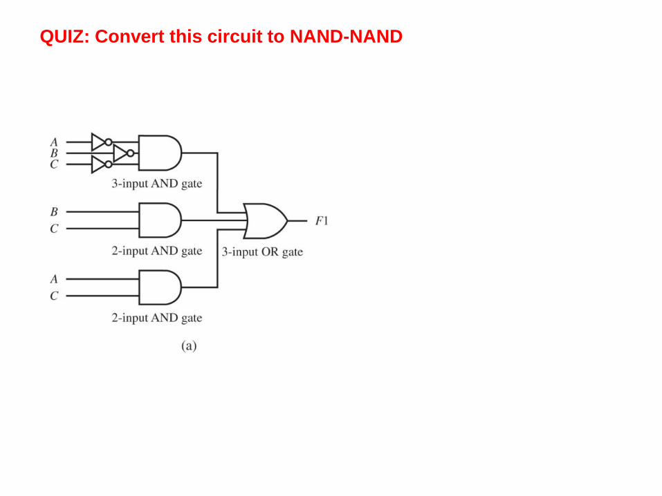
QUIZ: Convert this circuit to NAND-NAND

QUIZ: Convert this circuit to NAND-NAND
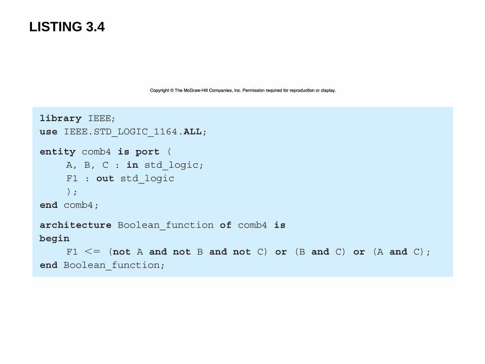
LISTING 3.4
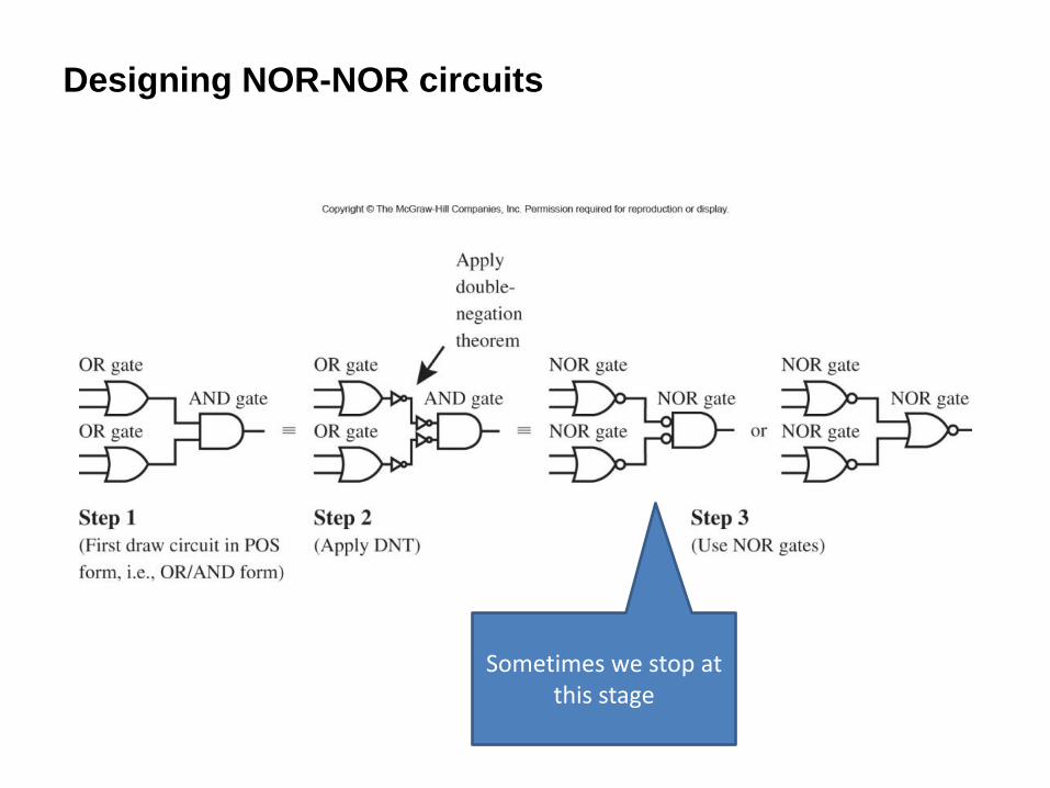
Designing NOR-NOR circuits
Sometimes we stop at this stage
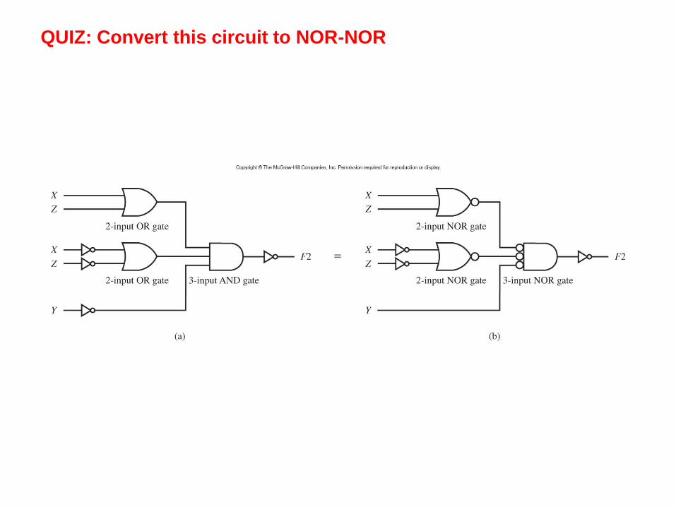
QUIZ: Convert this circuit to NOR-NOR
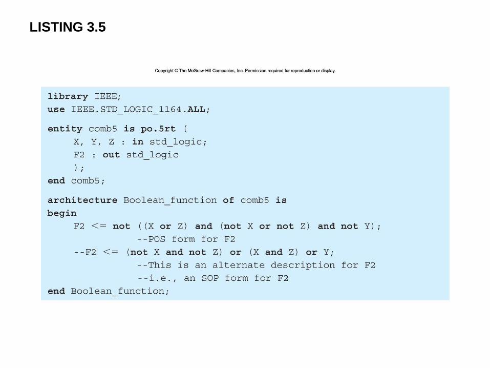
LISTING 3.5

To do for next time
• Read entire Sections 3.2, 3.3
• Read Section 3.4 (Generating …)
• Solve in notebook end-of-chapter 1-7 and 17.

QUIZ
In the first problem of Lab 3, we obtained this Boolean function: (A+B)∙(B+C)
Find it’s minimized S.O.P. form using:
• Truth table and K-map
• Boolean algebra manipulations
• Venn diagrams

QUIZ: Convert this circuit to NOR-NOR
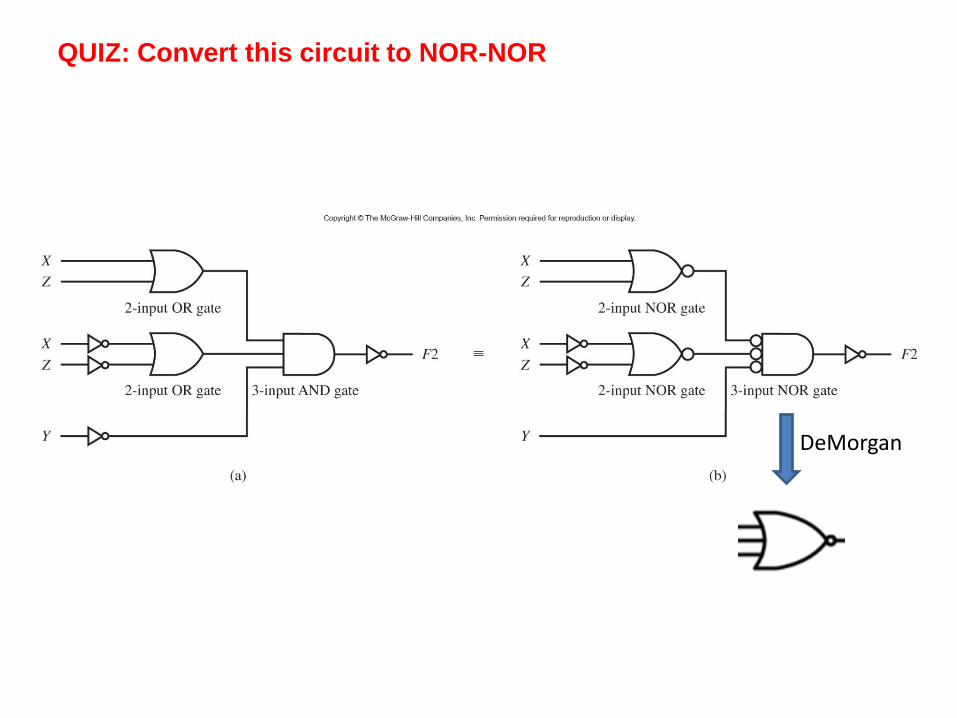
QUIZ: Convert this circuit to NOR-NOR
DeMorgan

3.6 Propagation delay
For a wire, it depends on 3 factors:
• Length
• Diameter
• Material:
• Au fastest, Ag next … but they’re both expensive
• Cu is next, but plentiful and easy to manufacture
• Al is slowest (poorest electrical conductivity), but 3
times lighter than Cu! So why not transition to Al
wiring?
http://www.picwire.com/technical/paper3.html

3.6 Propagation delay
For a gate, it’s more complicated …
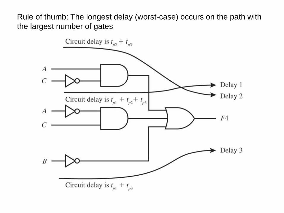
Rule of thumb: The longest delay (worst-case) occurs on the path with
the largest number of gates
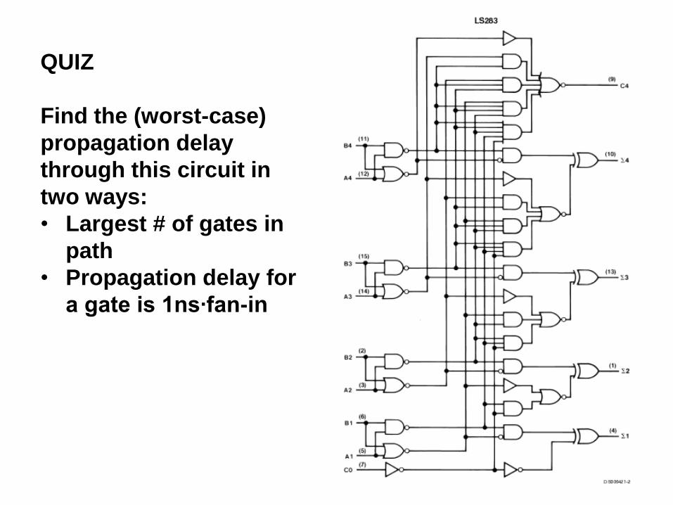
QUIZ
Find the (worst-case)
propagation delay
through this circuit in
two ways:
• Largest # of gates in
path
• Propagation delay for
a gate is 1ns∙fan-in

3.7 Decoders
Have you seen this type of products before?

TABLE 3.1

LISTING 3.6

WAVEFORM 3.3
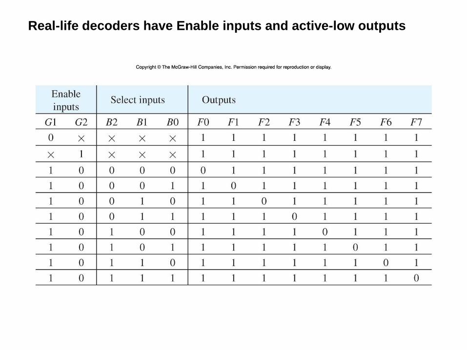
Real-life decoders have Enable inputs and active-low outputs

LISTING 3.7
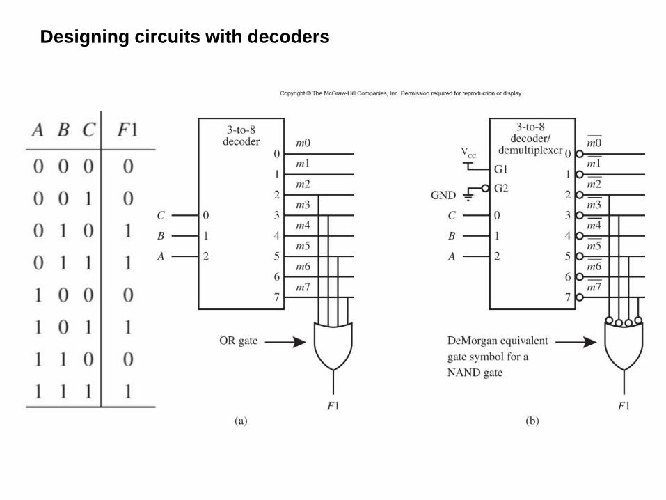
Designing circuits with decoders
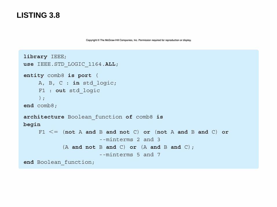
LISTING 3.8

Another option: design F inverted, then invert back at the end

QUIZ
Design a “2-out-of-3”
detector using the
decoder given:

This is the end of the material required for midterm

To do for next time
• Read entire Sections 3.5, 3.6, 3.7
• Solve in notebook end-of-chapter 39, 47-50, 54.
Monday lecture: review for midterm
Next week lab: midterm

QUIZ
Find the (worst-case)
propagation delay
through this circuit in
two ways:
• Largest # of gates in
path
• Propagation delay for
a gate is 1ns∙fan-in

QUIZ
Design a “2-out-of-3”
detector using the
decoder given: