Quantum transport in ballistic graphene devices...
113
Quantum transport in ballistic graphene devices A Dissertation Presented by Piranavan Kumaravadivel to The Graduate School in Partial Fulfillment of the Requirements for the Degree of Doctor of Philosophy in Physics Stony Brook University December 2015
Transcript of Quantum transport in ballistic graphene devices...

Quantum transport in ballistic graphene devices
A Dissertation Presented
by
Piranavan Kumaravadivel
to
The Graduate School
in Partial Fulfillment of the Requirements
for the Degree of
Doctor of Philosophy
in
Physics
Stony Brook University
December 2015

ii
Stony Brook University
The Graduate School
Piranavan Kumaravadivel
We, the dissertation committee for the above candidate for the
Doctor of Philosophy degree, hereby recommend
acceptance of this dissertation.
Xu Du – Dissertation Adviser Associate Professor, Department of Physics and Astronomy
Philip B. Allen – Chairperson of the defense Professor, Department of Physics and Astronomy
Harold J. Metcalf – Committee member Distinguished Teaching Professor, Department of Physics and Astronomy
Matthew Dawber– Committee member Associate Professor, Department of Physics and Astronomy
Fernando E. Camino – External committee member Staff scientist, Brookhaven National Laboratory
This dissertation is accepted by the Graduate School
Charles Taber Dean of the Graduate School

iii
Abstract of the Dissertation
Quantum transport in ballistic graphene devices
by
Piranavan Kumaravadivel
Doctor of Philosophy
in
Physics
Stony Brook University
2015
Graphene is a zero gap 2-D semiconductor having chiral charge carriers described by the massless relativistic Dirac-like Hamiltonian. In this thesis, unique transport properties that emerge from this energy spectrum are studied by using ballistic graphene and coupling its charge carriers with superconducting pair potentials and electrostatic gates.
Superconducting correlations can be induced in graphene by bringing it in contact with a superconductor. This superconducting proximity effect (PE) provides a way of exploring transport phenomena such as pseudo-diffusive behavior of ballistic carriers, specular Andreev reflections and unconventional quantum Hall effect with Andreev edge states. Hitherto, experimental realizations were limited by diffusive devices coupled to superconductors with low critical fields. In the first part of this work, in order to study these phenomena, we develop ballistic suspended graphene (G)-Niobium type–II superconductor(S) Josephson junctions. Our devices exhibit long mean free paths, small potential fluctuations near the charge neutrality point (CNP) and transparent SG interfaces that support ballistic supercurrents. In such a device, when the gate voltage is tuned very close to the CNP, unlike in diffusive junctions, we observe a strong density dependence of the multiple Andreev reflection features and normalized excess current. The observations qualitatively agree with a longstanding theoretical prediction for emergence of evanescent mode mediated pseudo diffusive transport. Next studying magneto-transport in these devices we find that PE is suppressed at very low fields even as the contacts remain superconducting. Further study reveals that distribution of vortices in the superconducting contacts affects the strength of the PE at the S-G interface.
The final part of the thesis searches for analogues of Klein tunneling in ballistic graphene by studying charge transport through an electrostatically created potential barrier. To this end, different device fabrication methods are developed to create ballistic heterojunctions on suspended graphene and graphene on hexagonal boron nitride using contactless ‘air’ local gates.

iv
To my parents….

v
Table of Contents
CHAPTER 1 .................................................................................................................................. 1
Introduction ................................................................................................................................... 1 1.1. Overview and outline of the thesis ................................................................................... 1 1.2. Theoretical overview of the properties of graphene......................................................... 4
1.2.1. The band structure of graphene using the tight binding approximation ................... 4 1.2.2. Chirality and the absence of backscattering.............................................................. 8 1.2.3. Density of states in graphene .................................................................................. 10
1.3. Overview of transport properties in graphene devices ................................................... 11 1.3.1. Graphene field effect gating.................................................................................... 11 1.3.2. Ballistic and diffusive transport in graphene .......................................................... 13 1.3.3. Substrate induced charge inhomogeneity ............................................................... 14 1.3.4. Quantum Hall effect in graphene ............................................................................ 15
CHAPTER 2 ................................................................................................................................ 17
Superconductor-graphene junctions ......................................................................................... 17 2.1. Superconducting proximity effect – A brief overview................................................... 17
2.1.1. Andreev reflection .................................................................................................. 17 2.1.2. The Blonder, Tinkham and Klapwijk model (BTK model) .................................... 19 2.1.3. Excess current ......................................................................................................... 21 2.1.4. SNS junctions: Multiple Andreev reflections (Sub harmonic gap structures) ........ 22 2.1.5. Andreev reflections in graphene – Retro and specular ........................................... 24 2.1.6. Andreev reflection in magnetic fields ..................................................................... 26
2.2. Fabrication of superconducting graphene (SGS) junctions............................................ 27 2.2.1. Suspended graphene superconductor junctions ...................................................... 27 2.2.2. Non-suspended superconductor- graphene devices ................................................ 35
2.3. Measurement setup and techniques ................................................................................ 35 2.3.1. He-3 Insert design and operation ............................................................................ 35 2.3.2. Measurement setup ................................................................................................. 36 2.3.3. Current annealing of suspended devices ................................................................. 37

vi
CHAPTER 3 ................................................................................................................................ 39
Signatures of pseudo-diffusive transport in suspended ballistic graphene superconductor junctions ....................................................................................................................................... 39
3.1. Theoretical Background: The gate dependent transmission in pristine graphene .......... 40 3.2. Proposals and requirements for experimental observations of pseudo-diffusive electronic transport .................................................................................................................... 43 3.3. Experimental methods and sample characterization ...................................................... 45 3.4. Probing specular Andreev reflection .............................................................................. 52
CHAPTER 4 ................................................................................................................................ 55
Magneto transport in type II superconductor –graphene Josephson weak links ................. 55 4.1. Introduction and motivation ........................................................................................... 55 4.2. Device fabrication and characteristics............................................................................ 57 4.3. Magnetic field measurements......................................................................................... 60 4.4. Discussion and future work ............................................................................................ 65
CHAPTER 5 ................................................................................................................................ 70
Fabrication of graphene heterostructures for Klein tunneling experiments ........................ 70 5.1. Klein tunneling of relativistic particles .......................................................................... 70 5.2. Klein tunneling in graphene ........................................................................................... 72 5.3. Experimental Studies of Klein tunneling in graphene heterostructures – a short overview of previous work ........................................................................................................ 76 5.4. Fabrication of ballistic graphene heterostructures ......................................................... 78
5.4.1. Fabrication of suspended graphene bipolar junctions with contactless gates ......... 78 5.4.2. Graphene/BN based heterostructures with triangular air top gates for Klein collimation ............................................................................................................................. 81
5.5. Experiment for demonstrating Klein collimation........................................................... 89 5.6. Other approaches to fabrication and future work ........................................................... 94
BIBLIOGRAPHY ....................................................................................................................... 97

vii
List of Figures
Figure 1.1: Atomic structure of graphene ....................................................................................... 5 Figure 1.2: Band structure of graphene with the low energy Dirac spectrum. ............................... 7 Figure 1.3: Illustration of the absence of intra-band elastic back scattering in graphene ............... 9 Figure 1.4 : Graphene field effect gating ...................................................................................... 12
Figure 2.1: An illustration of Andreev reflection at a Superconductor-Normal interface. ........... 19 Figure 2.2: Normalized differential conductance for different Z based on BTK model ............. 21 Figure 2.3: Excess current (Iexc) in SN junctions .......................................................................... 22 Figure 2.4: Sub harmonic gap structures due to multiple Andreev reflections (MARs) .............. 24 Figure 2.5: Illustration of retro and specular Andreev reflection ................................................. 25 Figure 2.6: Illustration of Andreev reflection in magnetic fields ................................................. 26 Figure 2.7: Etch free fabrication for suspended graphene – Superconductor junctions ............... 29 Figure 2.8: Stress tests for sputtered Nb films .............................................................................. 32 Figure 2.9: Components of the bottom end of the He-3 insert. .................................................... 36 Figure 2.10: Setup used for low temperature measurement of differential resistance as a function of Vbias at different gate voltages. .................................................................................................. 36
Figure 3.1: Ballistic and evanescent transport in graphene. ......................................................... 42 Figure 3.2: Device characteristics- Ballistic suspended graphene Josephson weak link .............. 47
Figure 3.3: Normalized differential resistance dIdV
RN
1vs. Vbias for different
F
F
vLE
! N .............. 48
Figure 3.4: Normalized Excess current (IexcRN) as a function of F
F
vLE
! N ................................ 50
Figure 3.5: Differential conductance curves for specular Andreev reflection .............................. 53 Figure 3.6: Differential resistance vs. Vbias for EF≤5 meV at T=1.5K .......................................... 54
Figure 4. 1: Properties of non-suspended NbN-graphene Josephson weak link........................... 58 Figure 4. 2: Differential resistance (dV/dI) vs Vbias of a 10 μm wide graphene- NbNJosephson junction ......................................................................................................................................... 59 Figure 4.3: Multiple Andreev reflections in NbN-graphene Josephson weak links ..................... 60 Figure 4.4: Zero field cool differential resistance measurements ................................................. 61 Figure 4.5: IexcRN vs. magnetic field (B) for zero field cool- ramp up measurements. ................ 62 Figure 4.6: Schematics of the three magnetic field ramping procedures ...................................... 63 Figure 4.7: Comparison of the differential resistance curves at B=200mT for the three magnetic field ramping procedures .............................................................................................................. 64 Figure 4.8: Comparison of excess current vs B for the three field ramp procedures ................... 64

viii
Figure 4.9: IexcRN vs B - for FC ramp up and down to test any impact from trapped flux in the superconducting magnet system. .................................................................................................. 67 Figure 4. 10: Differential resistance in the quantum hall regime of the suspended graphene Nb superconducting junction. ............................................................................................................. 69 Figure 5.1: Tunneling of Dirac particles of mass m across a. Klein (sharp) b. Sauter (smooth) potential step ................................................................................................................................. 71 Figure 5.2: Klein tunneling in graphene across a pn junction ...................................................... 73 Figure 5.3: Transmission as a function of incident angle θ for a bipolar graphene heterojunction........................................................................................................................................................ 75 Figure 5.4: Fabrication of suspended graphene with contactless air top gate (TG). .................... 79 Figure 5.5: AFM image of BN flake on SiO2. .............................................................................. 84 Figure 5.6: Preparation of MMA/tape/PDMS substrate for transfer. ........................................... 84 Figure 5.7: 2D materials transfer setup. ........................................................................................ 86 Figure 5.8: 2D materials transfer procedure ................................................................................. 88 Figure 5.9: Device for testing Klein collimation .......................................................................... 90 Figure 5. 10: Device characteristics of graphene on h-BN with triangular top gate. ................... 91 Figure 5. 11: Measurements for current splitting and Klein collimation ...................................... 92 Figure 5. 12: Ratio of resistance of the two branches used in the Klein collimation experiment. 93 Figure 5. 13 : Other possible fabrication approaches for graphene heterostructures. ................... 94 Figure 5. 14: Pseudo four terminal suspended graphene with superconducting NbN contacts over a ~70 nm thin local back gate. ...................................................................................................... 95

ix
Acknowledgements
First and foremost, I would like to thank my advisor, Xu Du, for his advice, support and
guidance throughout the past five years. Being one of his first students, I had the great fortune to
learn directly from him many of the skills that were essential in developing this thesis. Working
with him in setting up the lab, building, maintaining and troubleshooting equipment was a valuable
experience. Thank you for listening to my ideas, opinions and concerns with patience and for
motivating me to push forward during troubled times.
I would also like to thank my committee members for their time and effort in reviewing
my work and faculty members of the department who supported me at various junctures in this
journey. I owe special thanks to professors Matthew Dawber, Marivi Fernandez Serra, Harold
Metcalf, Philip Allen, Kostya Likharev, Dmitri Kharzeev and Laszlo Mihaly.
I had some wonderful time working with my group members Fen, Humed, Heli, Yan, Peter,
Naomi, Mike, Sid and Rick. Thank you all for the unforgettable memories and providing a lively
working environment. Bent Nielson has been a constant source of support from the time I joined
the lab. His knowledge of the resources in the department has been invaluable. And when
assistance was hard to find, he was always there to lend a hand. Thanks Bent for all your help.
I would like to acknowledge the support provided by the machine shop for their assistance
in building some of the equipment used in this work and the departmental staff, especially, Sara
and Pernille for their assistance in administrative matters and paperwork.
I had the good fortune to make some new friends and meet some great people at Stony
Brook. Thank you all for making my life at Stony Brook an enjoyable and worthwhile experience.
Finally I would like to thank my parents: Kumaravadivel (Appa) and Rajini (Amma) and
my brothers, Guruparan and Niruththan. Needless to say, without their love, support and
understanding this journey would have been difficult.

1
Chapter 1
Introduction 1.1. Overview and outline of the thesis
Research in graphene has broadened in scope since the first experiments were reported in
2004-5[1, 2]. There is now a great interest in graphene optoelectronics[3] and plasmonics.
Together with electronic properties, the thermal and mechanical properties of graphene have
inspired possibilities for diverse applications ranging from mobile phones, energy storage[4, 5] to
cancer treatment[6] and bio sensing[7]. Despite all this commercial prowess, the appeal of this
material, for me, is its relatively simple structure and the capability it provides in studying
relativistic quantum phenomena in benchtop experiments. So as a graduate student starting
research in 2010 (coincidently the year in which the Nobel prize was awarded for the discovery of
graphene) my natural choice was to work on projects that directly probe the fundamental properties
of the Dirac fermions in graphene.
Unlike semiconductor 2D electron gas systems (2DEGs) and other Dirac materials, the
massless Dirac charge carriers in graphene are easily accessible to experiments. It is convenient to
tune graphene’s carrier density and switch the carrier type by designing electrostatic gate
potentials. The electrons in graphene can also be directly coupled to a wide range of materials,
from metals to layered semiconductors [8-10]. But to study the intrinsic electronic properties
arising from its gapless relativistic-like spectrum requires disorder-free samples with low energy
fluctuations. One of the major steps in achieving this is by suspending graphene and relieving it
from the coarse substrate (silicon dioxide) that it sits on[11, 12]. Still, maintaining these qualities
while coupling it to various materials and electrostatic potentials, is technically challenging. The
very fact of the ease in accessibility of the electrons also makes it vulnerable to even the slightest
of extrinsic charges and impurities.

2
This theses work is on overcoming these challenges to study ballistic quantum transport of
Dirac fermions in graphene when 1) in contact with a superconductor and 2) under the influence
of engineered electrostatic barriers. In both these cases the process that reveals the interesting
physics involves electron-hole conversion. In the first case, the conversion occurs when scattering
from a superconducting pair potential and in the second case, the conversion occurs during head
on collisions on repulsive electrostatic barriers. In graphene the electron hole symmetry and
chirality makes these processes unique compared to those in normal metals and semiconductors.
Coupling two types of electron systems – the relativistic charge carriers in graphene with
strongly interacting Cooper pair condensates in a superconductor provides opportunities to test
various longstanding phenomena such as specular Andreev reflection[13], pseudo-diffusive
dynamics of ballistic carriers[14, 15] and to study graphene’s anomalous quantum Hall effects
infused with superconducting correlations[16, 17]. Chapters 2 and 3 focus on work on these topics
using graphene with transparent superconducting contacts. Chapter 2 presents a brief theoretical
overview of the superconducting proximity effect (and Andreev reflection processes), the
mechanism by which superconducting correlations are infused in graphene (and other normal
metals) from the superconducting leads. The unique Andreev reflection processes in graphene
especially near the Dirac point are highlighted. The rest of the chapter discusses the fabrication of
ballistic suspended graphene- type II superconductor devices with transparent interfaces. Even
though diffusive graphene-superconductor devices were studied almost six years ago [18-21], the
fabrication of ballistic superconductor junctions have remained challenging. The procedures
employed to free graphene from disorder posed challenges to the transparency of the
superconductor-graphene interface. Effectively combating such challenges culminated in the
development of the fabrication procedure described in the chapter. This is a crucial part of the
work that made possible the experiment presented in chapter 3 and potentially can form the basis
for many interesting studies in the future.
Chapter 3 of the thesis discusses work based on ballistic suspended graphene Niobium
superconductor devices. Here we explore intrinsic transport near graphene’s charge neutrality
point where carrier density almost vanishes. Inducing superconducting correlations in ballistic
graphene, we demonstrate evidence for transition from ballistic, propagating mode transport at
high carrier densities to pseudo-diffusive, evanescent mode transport at low carrier densities (near

3
the neutrality point). Also we probe inter-band (specular) Andreev reflections i.e., superconductor
induced reflection processes that couple electrons and holes from the conduction and valence band
of the Dirac cone.
Type II superconductors with a transparent interface on ballistic graphene provides the
opportunity to study induced superconductivity in the quantum hall regime (Andreev edge states).
But, intriguingly, even as the superconductor retains its properties to very high fields, the expected
evidence for Andreev edge states in graphene[22] is lacking[23, 24]. The devices studied in this
thesis work also show similar results. In Chapter 4 we explore this issue by performing low field
magneto-transport measurements in superconducting NbN- graphene junctions. By changing the
way the magnetic field penetrates the superconductor, we reveal that the vortex screening currents
in the superconducting NbN affect the Andreev reflection probability at the graphene-
superconductor interface. According to our present understanding this suppression is significant
when a reduced superconducting gap is present at the interface.
Chapter 5 of this thesis deals with the subject of transmission of massless Dirac particles
through potential barriers. Charge carriers governed by non-relativistic quantum mechanics, when
incident on a potential barrier, have a small probability of tunneling through. But the massless
Dirac-like quasiparticles of graphene have perfect transmission at normal incidence[25], a property
that has parallels to the Klein tunneling of spin ½ particles described by quantum
electrodynamics[26]. In graphene this is a consequence of conversation of pseudospin – a quantity
arising from the sub-lattice symmetry in graphene. The perfect transmission at normal incidence
through electrostatic barriers can be used to collimate randomly oriented electron trajectories and
guide them in a desired direction. Sharper potentials can also be used in negative index of
refraction experiments [27, 28]. The first part of chapter 5 presents a brief theoretical overview of
Klein tunneling and discusses previous experimental work on the subject. The rest of the chapter
is dedicated to the fabrication procedures and preliminary experiments that attempt to study Klein
tunneling in suspended graphene and hexagonal boron nitride (h-BN) supported graphene devices
with contactless local top gates. Contactless top gates are like bridges that cross over the
(suspended) graphene and are used to create the local electrostatic barrier. The h-BN supported
graphene devices are known to display almost the same ballistic properties as suspended graphene
devices and have no size limitations[29]. Therefore they are ideal for these electron collimation

4
experiments. The chapter also includes details of the transfer setup and procedure that was
developed to make the h-BN supported graphene devices.
In the rest of this chapter I provide a brief overview of the theoretical aspects of graphene and
its transport properties. The intention is to provide some background relevant to the experiments
discussed in chapters 3, 4 and 5. Further details on the topics discussed in this chapter and in the
beginning of chapter 2 can be found in a number of review papers [30-33].
1.2. Theoretical overview of the properties of graphene
1.2.1. The band structure of graphene using the tight binding approximation
Graphene is a single sheet of identical carbon atoms arranged periodically to form a two-
dimensional hexagonal lattice structure. Each carbon atom with four valence orbitals forms two
kinds of bonds with their three nearest neighbors. One is the strong in-plane σ bonds formed by
sp2 hybridization of the s, px and py electron orbitals. The other is the π-bond formed by nearest
neighbor covalent bonding of the delocalized pz orbitals. The σ bonds are responsible for the
strength and stability of graphene whereas the π bonds govern the unique low energy electronic
properties of graphene. The honeycomb lattice by itself is not a Bravais lattice but can be visualized
as two part triangular Bravais sub-lattices, labelled A (red) and B (blue) in figure 1.1. Each carbon
atom in one sub-lattice is surrounded by indistinguishable carbon atoms from the other. This
symmetry, as we will see later, has interesting implications to the dynamics of charge carriers in
graphene.

5
Figure 1.1: Atomic structure of graphene. (left) Hexagonal lattice graphene showing the two sub lattices A and B. (right) First Brillouin zone with the symmetry points Γ, M, K (and K’).
The unit vectors of one of the Bravais lattices (sub lattice A in figure 1.1) and the corresponding
reciprocal lattice vectors can be written as,
� �3,321aa
& and � �,3,3
22 � aa& (1.1a)
� �3,332
1 ab S
& and � �3,3
32
2 � a
b S& (1.1b)
and the vectors to the nearest neighbor (B sub-lattice) atoms are given by,
� �,3,121a
G&
� �3,122 � aG
& � �0,13 a� G
& (1.2)
Here a=1.46A0 –is the lattice separation. The first Brillouin zone is hexagonal and is shown in
figure (1.1(b)). Γ, Κ and Μ represent the high symmetry points. Although there are six K-points
corresponding to the six corners of the Brillouin zone only two are inequivalent. The others are
displaced by reciprocal lattice vectors. The two distinct K points, commonly labelled K and K’,

6
are called ‘valleys’ or ‘Dirac points (DPs)’. This is because of their unique position in graphene’s
linear energy spectrum. The coordinates in reciprocal space for the two valleys are
¸¹·
¨©§
aaK
332,
32 SS&
, ¸¹·
¨©§ � c
aaK
332,
32 SS&
(1.3)
The covalent bonding of the π-orbitals is sufficiently strong to use the tight binding approach for
evaluating graphene’s energy spectrum. The nearest neighbor tight binding Hamiltonian, in the
basis of the π orbital wave functions BA << , of sub lattices A and B, is given by
¸¸
¹
·
¨¨
©
§ ¦
¦� 0
0.
.
jki
jki
j
j
e
etH
G
G
&&
&&
�, where j=1, 2 and 3. (1.4)
Here t ~3eV is the nearest neighbor hopping parameter. The eigenvalues of the Hamiltonian is
given by,
¸¹
ᬩ
§�¸¸¹
·¨¨©
§¸¹·
¨©§�r r y
yx kaakaktkE23cos4
23
cos2
3cos41)( 2&
(1.5)
and the plot of the band structure is shown in figure 1.2. It can be seen that the above energy
spectrum is electron-hole symmetric very close to the two K points with vanishing energies:
0)()( c KEKE&&
. This degeneracy is robust due to time reversal and C3 symmetry of the lattice.
Breaking this symmetry requires a periodic potential that acts on the sub lattice space.

7
Figure 1.2: Band structure of graphene with the low energy Dirac spectrum near the K valleys. The π and π* band are bonding and antibonding orbitals and represent valence and conduction bands near the K valley. Figure on left obtained from [34].
Now expanding equation (1.4) at the K point for small values of kKq*&&
� the low energy
Hamiltonian can be written as
pvH F&&�
.V (1.6)
where qp &!
& ,
23tavF and � �yx VVV ,
& is a vector of Pauli matrices. The corresponding
Hamiltonian for K’ is pvH F&&�
.*V with )( ' kKqp&&
!&
!&
� . The low energy eigenvalues at
each valley is a linear function of momentum:
pvpE F&
r )( (1.7)
Equation (1.6) resembles the Dirac[35] equation in 2D for ultra-relativistic massless fermions with
a velocity vF =c/300 where c- the speed of light in vacuum. The ± values correspond to the π and
q
E
Conduction Band
Valence Band
Dirac point
EF =0

8
π* bonds and refer respectively, electron and hole-like excitations near the K valley (see Figure
1.2). The corresponding eigenfunctions describing the Dirac like quasi particle excitations at K
and K’ are:
� �¸¸
¹
·
¨¨
©
§
r ¸
¹
ᬩ
§ <
�
r
2
2
21
T
T
\\
T i
i
KB
KAK
e
e (1.8.a)
� �¸¸
¹
·
¨¨
©
§
r ¸
¹
ᬩ
§ < �
c
crc
2
2
21
T
T
\\
T i
i
BK
AKK
e
e (1.8.b)
where ¸¸¹
·¨¨©
§
y
x
qqarctanT . Note that the above wave functions at K and K’ are related by a time
reversal symmetry with a reflection in k-space along kx about the M-point in figure 1.1. The wave
functions are two component spinors – they have a Berry phase of π. The two components,
however, do not represent the real spin of electrons but from the two sub lattices. The Pauli matrix
operators in equation (1.6) are therefore referred to as ‘pseudospin’ operators. They operate on the
sub-lattice degree of freedom.
1.2.2. Chirality and the absence of backscattering
The Dirac-Weyl equation (massless Dirac equation) in QED describes two types of
particles described by a quantity known as chirality (or helicity for massless spin ½ particles). The
chirality operator is defined as: ph ˆ.21ˆ V& where p is the unit vector in the direction of
momentum. For graphene’s Hamiltonian in (1.6), > @hH ˆ,ˆ =0. Therefore chirality is a conserved
quantity. It describes the projection of pseudospin on the direction of momentum. The chirality
operator acting on the wave functions at K and K’ gives
� � � �TT rr <r < KKh21ˆ (1.9.a)

9
� � � �TT rrc < < '
21ˆ
KKh # (1.9.b)
In the K valley the electrons have right handed (positive) chirality whereas the K’ valley has
negative chirality. Electrons and holes of the same valley have also opposite chirality (see figure
1.3).
Figure 1.3: Illustration of the absence of intra-band elastic back scattering in graphene for electrons. The electron momentum for backscattering flips from q to –q (alongÆ direction). Here h represents chirality and σ represents pseudospin (colored to represent the sub-lattices A and B). The intra-valley back scattering (light blue curled arrow) cannot happen since the electron has to flip pseudospin i.e., blue branch to red branch of the spectrum. Inter-valley scattering (purple arrow) cannot happen because it will violate chiral conservation.
Pseudospin and chirality have important consequences on scattering in graphene. Consider
Hamiltonian (1.6) with a scatter potential IrVrV ˆ)()(ˆ where I - unit matrix. This potential does
not operate on the sub lattice space i.e., it does not couple the sub lattices. Then the probability for

10
intra-valley elastic back-scattering ( qq &&�o ) is zero since the pseudospin that is coupled to the
momentum cannot be flipped. For K valley this can be shown from equation (1.8.a) as
� � � � � � � � 0()(()()( <<v�<< ���� TTSTT qqiqrVq KKKK&&&& . (1.10)
More generally using the first Born approximation, for ri qq && , the scattering probability as a
function of the angle between the incident and scattered electron φ can be written as
� � � � TM 22cos~)()(
riqqrKiK VqrVqP &&&&
<< �� (1.11)
Similarly for potentials that do not act on the valley space, inter-valley backscattering is prohibited
because of chiral conservation (Figure 1.3). From equation (1.8)
� � � � � � � � 0()(()()( ' <<v�<< ���� TTSTT qqiqrVq KKKK&&&& (1.12)
Suppression of backscattering gives rise to weak anti-localization in graphene [36-38]. It also has
interesting consequences on the ballistic propagation of electrons across a pn junction: The
transmission across a potential is perfect similar to the Klein tunneling of relativistic particles
across a strong repulsive electrostatic barrier[25]. The experiments exploring this phenomena are
discussed in Chapter 5.
1.2.3. Density of states in graphene
Using equation (1.7) and accounting for spin and valley degeneracy, the number of states in the
reciprocal space in graphene is given by:
2
2)( ¸¹
ᬩ
§
FvE
qn!S
(1.13)
which gives the density of states per unit area:

11
� �221)(
FF vE
dqdn
vED
!! S ¸
¹
ᬩ
§ (1.14)
The density of states in graphene is linear in energy and vanishes at DP. This is different from the
energy-independent D(E) in non-relativistic 2DEG systems. Even though the carrier density
vanishes at the DP, the conductivity has a quantum limited universal value of the order 4e2/h.
1.3. Overview of transport properties in graphene devices
1.3.1. Graphene field effect gating
One of the conveniences in studying electronic properties of graphene is the capability of
using a single gate electrode to create a field on the surface electrons and tune the Fermi energy
(EF) from conduction to valence band and vice versa. The relation between EF and the carrier
density (n) follows from equations (1.7) and (1.13) and is given by
SnvE FF ! (1.15)
where SnkF . Graphene devices are made by deposition of graphite flakes on Si/SiO2
substrates. The Si is electron doped and serves as the gate electrode. The SiO2 is the gate dielectric.
In the case of suspended graphene the gate dielectric is vacuum. The gate voltage is applied
between the gate and one of the grounded electrodes in contact with the graphene flake (see figure
1.4).The relationship between the gate voltage (Vg) and n is given by edVVeACn grgg /)/( 0HH
where Cg is the gate capacitance, A is the gate area, εr is the relative dielectric constant and d is the
thickness of the gate dielectric. The gate capacitance is usually the geometric capacitance (when
the gate dielectric is thin, the quantum capacitance should be considered in series with the
geometric capacitance).

12
Figure 1.4 : Graphene field effect gating. a. Schematics of a device showing the gate capacitance and the ambipolar resistance vs. gate voltage. b. Conductivity σ as a function of carrier density (n) for a ballistic sample (plotted on a log-log scale) showing n1/2 behavior at high carrier density and saturates to a constant below the minimum carrier density nsat.
The gate voltage dependence of the resistance of an undoped ballistic device is shown in
figure 1.4. The DP is at Vg=0V where the resistance is maximum. Also the resistance is symmetric
about the CNP reflecting the electron-hole symmetry of the low energy spectrum in equation (1.7).
In experiments doping from impurities from the fabrication process can result in a non-zero gate
voltage. This value varies from sample to sample and can be either positive or negative i.e.,
electron or hole doped. The metal contact leads can also infuse additional charge carriers in
graphene forming a gate tunable pn junction near the leads[39]. This can cause the gating curve to
become asymmetric.

13
1.3.2. Ballistic and diffusive transport in graphene
The conductance in a pristine graphene sheet can be calculated using the Landauer formula
¦ nTheG
24 . Here the factor of 4 is for the spin and valley degeneracy in graphene.
Transmission in the ballistic regime is given by NheG
24 where N~W/λF is the number of modes
at large Fermi energies. Here λF – is the Fermi wavelength and W- width of the graphene sheet.
Using equation (1.15), the ballistic conductivity has the following relation:
nEF ~~V (1.16)
This relation breaks down when nÆ 0 at the DP. This is because, close to the DP,
evanescent mode transport dominates over the propagating modes. Theoretically, this regime is
identified as pseudo-diffusive where, even when the charge carriers are classically ballistic, their
quantum transport is indistinguishable from that in diffusive metals. At DP, under certain
conditions, evanescent transport alone prevails. Also the transmission is unity- a characteristic that
can be related to the absence of backscattering in graphene. Several proposals exist that have
highlighted on transport signatures relating to this unique behavior in graphene but several
technical challenges have made experimental observations difficult. Details on this topic and some
experiment evidence that shows the first hints of the transition from ballistic to pseudo diffusive
like behavior is the subject of chapter 3.
Equation (1.16) implies that the mobility in ballistic graphene, nne1~~ VP is density
dependent. Due to the same reasons as mentioned above, the mobility at low n diverges due to the
vanishing DOS and cannot be used for estimations near the DP. Also in real samples the ballistic
relation fails due to the presence of small, but finite, potential fluctuations (electron-hole puddles)
close to DP. Potential fluctuations are strongly enhanced due to topological corrugations and
charge impurities [40, 41]. So the maximum mobility reported in ballistic sample is at the
minimum carrier density n=ns, where the slope of the μ vs. n curve begins to deviate from -1/2 (see

14
figure 1.4). Alternatively mobility and minimum carrier density (ns) can be estimated by quantum
Hall (QH) measurements. The ballistic mean free path lm =Fke
h22V is also defined for densities above
ns. In ballistic samples the mean free path is only limited by the length of the sample.
In diffusive samples the conductivity is calculated using the Boltzmann equation:
2)()(22
FFFF kEDve WV (1.17)
Here kF is the Fermi wave vector and D(EF) and τ(EF) are the density of states and scattering time
at the Fermi level respectively. Several sources of impurities and defects contribute to diffusive
transport in graphene. The most common type of scattering in graphene devices is charge impurity
Coulomb scattering. Due to the presence of Coulomb scatterers it can be shown that, nvV [42-
44] making the mobility independent of n and the mean free path increase with n. This is what is
usually seen in graphene on SiO2 samples including the earliest experiments [45, 46]. For short
range scatterers, such as lattice scale defects, conductance does not significantly depend on n.
Other sources for diffusive transport include phonon scattering and formation of mid gap states by
defect induced bound states[47]. Since the time scale of the scattering mechanisms is dependent
on Fermi energy, their influence on the gating curves will vary at different Vg. The overall effect
from the different mechanisms on the experimental R(Vg) can be fitted using the Mathiesson’s rule.
Mean free path and mobility are estimated by the Drude model.
1.3.3. Substrate induced charge inhomogeneity
Long range Coulomb scattering from trapped charged contaminants between the substrate
and graphene[40], the substrate roughness[48], dangling bonds[49] and defects can dope graphene
and split the zero density DP into puddles of electrons and holes. This DP regime is commonly
known as the charge neutrality point (CNP) to distinguish it from the ideal DP. Due to the
fluctuating puddle densities, in the commonly used substrate SiO2 the energy smear at CNP (δES)
~ 30meV to 100meV. This makes it impossible to study ballistic transport at low n and intrinsic
physics at the DP. Two popular techniques have emerged over the years that attempted to reduce

15
the effect of the substrate with great success. One is to suspend graphene between the metallic
contacts by etching away the substrate underneath [11, 12]. The other is by using hexagonal boron
nitride (h-BN), a 2-D substrate with reduced surface roughness and hexagonal lattice structure
similar to graphene. Suspended graphene shows high mobility and low ns after current annealing
(see 2.3.3). And to this date, suspended graphene is best for studying transport near the CNP at
densities ns ~ 108- 109 cm-2[12] (potential fluctuations ~5meV). The main limitation of suspended
graphene samples is the size. Suspending graphene for electronic devices with large dimensions
and different geometries with non-invasive electrodes (like Hall Bar geometries) is technically
challenging. Fabrication of graphene on h-BN has improved over the years since it was first
developed and generally it can attain high nobilities and long mean free paths[50]. And since
graphene is substrate supported there are no device-size limitations. But generally in graphene/h-
BN the potential fluctuations ~10meV, slightly higher than suspended graphene.
1.3.4. Quantum Hall effect in graphene
Given the linear gapless spectrum and chiral nature of the quasiparticles in graphene, the
QH effect has anomalous features distinguishable from conventional semiconductor 2D electron
gas (2DEG) systems [46, 51]. In the presence of a field B, replacing Aepp&&&
�o in equation (1.6)
and using the Landau gauge for writing the vector potential xByA �&� , the eigenenergies of the
Landau levels can be obtained. It is written as:
BjvejsignE Fn22)( ! where ...3,2,1,0 j (1.18)
The Landau spectrum is jv , which is unlike the 2D semiconductor Landau level spectrum:
)2/1( � jE cn Z! , where ωc is the cyclotron frequency. Also, in graphene there is a zero energy,
electron-hole degenerate Landau level. The electron excited Landau edge states above E=0 share
their energy with hole edge states below E=0, resulting in the characteristic half-integer QH effect.
The Hall conductance in monolayer graphene is

16
,..2,1,0;)21(4
2
� jhejGxy (1.19)
The filling factor ...10,6,2)21(4 � j
eBnhQ , where h- Planck constant and n- carrier density. The
quantized values in bilayer graphene: ,..2,1,0;)1(42
� jhejGxy . This difference can be used to
identify graphite flake is single or bilayer graphene.
From equation (1.18), the requirement to see at least one QH plateau in pristine graphene
is set by the following: )(3501 TBmeVEE � . Therefore for B>1T, integer QH effect can
emerge at room temperature for samples with a maximum δES ~30 meV. But disorder smears the
Landau levels and fields around 30T are normally required[45]. In suspended graphene with δES
<5 meV, QH features should be easily observable ~ 1T. At low temperatures, in the best suspended
samples, QH plateaus can fully develop at a few hundred mTesla. For fractional QH effect, the
separation between Lambda levels is smaller: <5meVs for B=1T [52-54] and with currently
available magnetic fields, ballistic samples are normally required.
Other than thermal effects, for QH plateaus to develop the scattering time (τ) > the time
required to complete one cyclotron orbit: ωcτ >1 (or equivalently, the mean free path lm> magnetic
lengtheBh
). In most SiO2 based graphene devices, even at low temperatures, the required fields
to observe well developed QH plateaus are higher than the theoretical values because of impurity
scattering and substrate inhomogeneity.
So it is clear that ballistic graphene devices with high mobility, long mean free path and
low potential fluctuations are essential to study intrinsic properties near the Dirac point as well as
QH effect at low fields. Low field QH and fractional QH effect are ideal to study the coexistence
of superconductivity with the Landau spectrum since most superconductors that can be used as
contacts on graphene and 2DEGs lose their superconductivity at few Tesla (for example Nb the
upper critical field is ~3.5-4T).

17
Chapter 2
Superconductor-graphene junctions
Superconductivity can be induced in normal metals by bringing them in contact with a
superconducting material so that the coherence of the Cooper pair condensate diffuses into and
survives in the normal material. Merging the relativistic Dirac fermions in graphene with
superconducting correlations can lead to many interesting phenomena. Pseudo-diffusive dynamics
of ballistic charges[14, 15], specular Andreev reflection[13], induced superconductivity under
magnetic fields and in the QH regime[22] are some of the interesting phenomena that remain to
be observed experimentally. In Chapters 3 and 4 many of these phenomena will be explored using
graphene -type II superconductor devices. As a prelude, the first half of this chapter will briefly
outline the basic features of superconducting proximity effect, and highlight features that are
unique to graphene. The fabrication of ballistic superconductor graphene devices is crucial for
observing many of the phenomena stated above. Even though most of these were predicted within
years after the discovery of graphene in 2004, several technical challenges have made experimental
realization impossible. The latter half of the chapter will detail how such samples are fabricated
using suspended graphene. At the end of this chapter the experimental measurement setup used to
characterize these devices is presented.
2.1. Superconducting proximity effect – A brief overview
2.1.1. Andreev reflection
When a superconductor (S) is in perfect contact with a normal metal (N), an electron with
energy (E) above EF but within the superconducting gap (Δ) cannot transmit since there are no
quasi-particle states within the gap. In such cases charge transmission occurs by a process called
Andreev reflection (AR) where an electron (hole) entering the superconductor (S) from the normal
metal (N) gets reflected as a hole (electron) so that a Cooper pair can form inside S. So effectively

18
a charge of 2e gets transferred across the SN interface. The electron and hole excitations involved
in AR are from the conduction band (CB). Since a CB hole moves opposite to the direction of its
wave vector, the hole retraces the path of the incident electron and hence the reflection is retro
(Figure 2.1)1.
The Andreev quasiparticle excited states at the SN interface are described by the
Bogoliubov deGennes (BdG) equation [55],
(2.1)
where H –is the free electron Hamiltonian for the N-side and (u,v) – represents the electron-like
and hole wave functions and T is the time reversal operator. The reflected quasiparticle state is a
time reversed state of the incident quasiparticle with a fixed phase relation determined by their
energy with respect to Δ. If the superconductor used is an s-wave superconductor the net spin of
the Cooper pair is zero and the Andreev quasiparticles will have opposite spins.
The phase conjugated Andreev pair can propagate into the N region extending up to a
distance known as the coherence length (ξ)'
Fv!~ . The spilling of this coherence from the
superconductor across the interface and into the normal metal is commonly known as the
superconducting proximity effect(PE)[33]. By the Andreev process the superconductor draws a
charge of 2e for each incident charge e. So it follows that when E<Δ, the conductance of the
interface is twice of that when the superconductors become normal.
1 Note that in the illustration in figure 2.1 a step like function for the gap is used at the SN interface.
This assumption is only valid in cases where ‘bulk’ superconducting contacts are directly in contact with a normal metal.
¸¹
ᬩ
§ ¸
¹
ᬩ
§¸¹
ᬩ
§�'
'�� v
uE
vu
ETHTEH
F
F1

19
Figure 2.1: An illustration of Andreev reflection at a Superconductor-Normal interface.
2.1.2. The Blonder, Tinkham and Klapwijk model (BTK model) In experiments the SN interface is not ideal for complete AR. Even when the E<Δ, normal
scattering processes can happen. The BTK model is a widely used microscopic theory that in-
cooperates the elastic scattering processes due to Fermi velocity mismatch and impurities to
calculate the current-voltage (IV) characteristics of the SN interface [56]. The scattering potential
is modelled by a delta function potential at the interface. Here Z is known as
the dimensionless barrier strength.
Solving the BdG equations with V(x) [33], the current flow through the SN interface can
be written as,
)()( xvZxV FG!
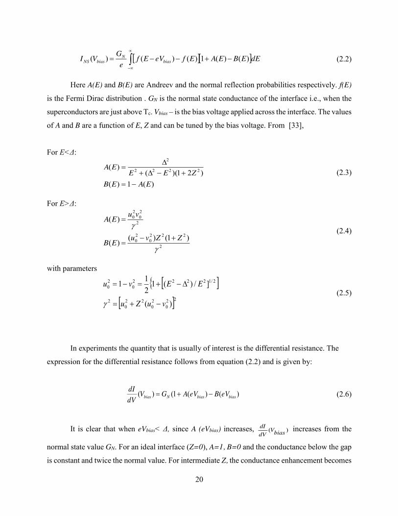
20
(2.2)
Here A(E) and B(E) are Andreev and the normal reflection probabilities respectively. f(E)
is the Fermi Dirac distribution . GN is the normal state conductance of the interface i.e., when the
superconductors are just above Tc. Vbias – is the bias voltage applied across the interface. The values
of A and B are a function of E, Z and can be tuned by the bias voltage. From [33],
For E<Δ:
(2.3)
For E>Δ:
(2.4)
with parameters
(2.5)
In experiments the quantity that is usually of interest is the differential resistance. The
expression for the differential resistance follows from equation (2.2) and is given by:
)()(1()( biasbiasNbias eVBeVAGVdVdI
�� (2.6)
It is clear that when eVbias< Δ, since A (eVbias) increases, )( biasVdVdI increases from the
normal state value GN. For an ideal interface (Z=0), A=1, B=0 and the conductance below the gap
is constant and twice the normal value. For intermediate Z, the conductance enhancement becomes
> @> @dEEBEAEfeVEfe
GVI biasN
biasNS )()(1)()()( ���� ³v
v�
)(1)()21)((
)( 2222
2
EAEBZEE
EA
� ��'�
'
2
2220
20
2
20
20
)1()()(
)(
J
JZZvuEB
vuEA
��
> @^> @22
020
220
2
2/122220
20
)(
]/)(1211
vuZu
EEvu
��
'�� �
J

21
weaker and less abrupt. This is because the increase in A(E) is mitigated by finite normal scattering
probability B(E). For higher Z (strong barrier or tunnel junctions) A(E) is completely suppressed
and )( biasVdVdI below Δ can decrease substantially reaching zero in ideal tunnel barriers with no
thermal induced hopping. The differential conductance for different Z calculated by BTK is
presented in figure 2.2,
Figure 2.2: Normalized differential conductance curves for different values of Z based on the BTK model. The plots are from [56].
2.1.3. Excess current
The DC current voltage (IV) curve of a transparent SN junction does not follow a linear
Ohmic relation V=IRN where GN=1/RN. This is because additional current flows through the SN
interface due to the proximity effect when eV<< Δ. The linear fit for the IV curve for eVbias>> Δ,
has a slope GN with a non-zero intercept at V=0. The value of the intercept is the excess current
(Iexc). The expression for the excess current can be written as[56]

22
, (2.7)
where . For a fixed temperature is only a function of Z. The dependence
of Iexc on Z for T=0 is shown in Figure 2.3(a) and the method to calculate excess current from an
IV plot is shown in Fig 2.3 (b). Using the value of the excess current, the strength of the proximity
effect of a junction can be evaluated.
Figure 2.3: Excess current (Iexc) in SN junctions: a. Iexc as a function of Z. b. IV curves for junctions with different Z at T=0K. The red dotted line is a linear fit for curve Z=0.5. The black dotted line represents the Ohmic curve with zero intercept. Both lines have a slope of RN. The plots were adapted from reference [56].
2.1.4. SNS junctions: Multiple Andreev reflections (Sub harmonic gap structures)
In a normal metal separated by two superconducting contacts (SNS junctions), the excess
current is almost twice of that of the SN junction[57]. In SNS junctions close to zero bias and when
ξ> L-length of N channel, a Josephson supercurrent flows through the channel. This current has a
phase that is related to the phase difference of the two superconductors and is an AC current (The
excess current is a DC current and does not include the dissipationless AC current at zero bias).
³f
f��f�
'!!
� 0
)]()()([)](1[
1)( dEBEBEABeReV
IIIN
NNSNexc
)1()( 2
2
ZZB�
f'
Nexc RI

23
The AR processes takes place at finite biases and for SNS junctions this can happen when eVbias<
2Δ. The dip in occurs at Vbias= 2Δ/e(see figure 2.4 right).
Unlike in SN junctions, in SNS junctions when eVbias<2Δ, in the absence of any
decoherence mechanisms in the normal metal, the Andreev pair can traverse from the left
superconducting lead to the right and undergoes an AR again. The number of times the AR happens
reflect as harmonic oscillatory features in the DC IV characteristics. To understand the harmonics,
a simple way is to focus on the transport of a single electron in N between the two S-leads. Let
Vbias be the voltage bias between the two S-leads. When │eVbias│> 2Δ there is no Andreev process
and an electron just normally escapes from the left lead to the right lead. But if │eVbias│ = 2Δ then
at least a single AR becomes possible and an effective charge of 2e is transferred through the
junction. If 2│eVbias│ = 2Δ, AR happens twice, one at each lead. The charge transfer is now with
2x2e into the superconductors. This is illustrated in Figure 2.4. Decreasing Vbias further, more ARs
take place at the superconducting leads leading to more charge transfer in multiples of 2e. The Vbias
and the number of ARs (n) are related by the following equation:
neVbias
'
2 , where n=1,2,3 etc., (2.8)
The coherent sum of many such multiple AR (MARs) results in proximity effect with a
sharp dip in dV/dI at values of Vbias given by equation 2.8. These oscillatory signatures from MARs
are also known as sub harmonic gap structures (SHGS). Figure 2.4 shows an experimental curve
for an Al-graphene Josephson device at T=270mK. At-least three SHGS are discernible. The
vanishing dip at Vbias=0 is due to the onset of supercurrent. The number of SHGS that are
experimentally observable depends on thermal noise and the transparency of the interface.
The MAR dip features and normalized supercurrent (IcRN) are gate (density) independent
in diffusive samples. It was shown that the magnitude of the MAR dips were dependent on L/ξ,
where L- is the length of the junction and'
D![ – the coherence length in N. Here
2mF lvD is
the diffusive constant. This was confirmed with graphene-Al SNS junctions [20].
)( biasVdIdV

24
Figure 2.4: Sub harmonic gap structures due to multiple Andreev reflections (MARs): (left) Illustration for double AR i.e., 2Δ=2eVbias. (right) An experimentally measured normalized differential resistance vs. Vbias curve showing dips associated with MARs.
2.1.5. Andreev reflections in graphene – Retro and specular
Proximity effect in graphene can be described in the same way as in other metals by using
the BTK model. But replacing the Schrodinger equation with the Dirac Hamiltonian in the BdG
equation presents some additional properties that differ from normal metals.
As mentioned earlier, Andreev electron and holes are time reversed. So the
superconducting pair potential will couple states in graphene from the time reversed valleys – K
and K’. The quasiparticle electron-hole states (u,v) should then be described by the four component
spinor wave functions (u1,u2,v1,v2)= ),,,( *,
*,,, KBKAKBKA cc \\\\ . The time reversal operator
CTz
z¸¹
ᬩ
§
00V
V where C- charge conjugation operator[58]. In ballistic systems, the two valley
transport is intrinsic to graphene while in the normal state it is single valley transport. Although
presence of certain scatterers can couple valleys in diffusive systems, the resulting transport is not
intrinsic to graphene and is sample (or impurity) dependent [19]. The phase coherent two valley
transport has led to interesting proposals in the detection of valley polarization in ballistic graphene
[17].

25
Unlike in normal metals, in graphene the AR probability is unity even when Z is finite.
This is because AR does not flip pseudospin i.e., Andreev electrons and holes in graphene belong
to the same sub lattice. Backscattering without AR would require scattering to a different sub-
lattice. This will violate chiral conservation. Therefore the quasiparticle has no other way but to
undergo AR.
Another interesting phenomenon which is unique to a zero gap semiconductor like
graphene is that the ARs can be inter-band i.e., the electrons from the conduction band can Andreev
scatter as a hole in the valence band. This requires the Fermi energy (EF) < superconducting gap
(Δ). Since a valence band hole moves in the same direction as its wave vector, unlike in retro
reflection, only the velocity component perpendicular to the interface is flipped. As a result the
reflection becomes specular[13] (Figure 2.5). Exploring this experimentally is challenging since
it requires ultra clean samples with less energy smearing at CNP compared to the superconducting
gap which is typically a few meVs. Specular AR is explored experimentally at the end of Chapter
3.
Figure 2.5: Illustration of retro and specular Andreev reflection at a Superconductor (S) graphene (G) interface. C.B- conduction band, V.B valence band. v and k are group velocity and wave vector respectively. Here E=eVbias.

26
2.1.6. Andreev reflection in magnetic fields
With a type-II superconductor coupled to a normal metal, it is possible to retain the
superconducting properties of the lead at higher fields, up to the upper critical field of Hc2, while
studying the response of the Andreev pair in the normal metal. In retro AR the electron and hole
are from the same (say conduction) band. With negative mass and opposite charge, the cyclotron
orbit of the hole in a magnetic field has the same rotation as the electron. The situation is different
in graphene for specular (inter-band) AR, where the cyclotron orbits are opposite for electrons
and holes. Experiments can be designed in large scale ballistic devices that can detect these
spatially different cyclotron trajectories. The trajectories can be switched back and forth by tuning
the Fermi energy towards and away from the Dirac point. This is illustrated in figure 2.6.
Figure 2.6: Illustration of Andreev reflection in magnetic fields: a. and b. In low magnetic fields: Direction of electron and hole cyclotron orbits for specular (a) and retro (b) Andreev reflection. c. Formation of (Retro) Andreev edge states in the QH regime (high magnetic fields). Magnetic field is directed out of the paper.

27
Thin film type II superconductors support vortices at low magnetic fields. Their effect on
the Andreev pair at the interface is also an interesting question. This is discussed in Chapter 4. At
high magnetic fields when the bulk becomes insulating, alternating Andreev electron and hole
skipping orbits are formed at the superconducting interface. These are known as “Andreev edge
states”. Depending on the phase coherence of the Andreev pair on the normal side and the quality
of the interface, the presence of these Andreev edge states is expected to change the QH
conductance from conventional values. In the ideal case it is expected that the quantized
conductance values should double[22]. The effect of specular AR in the QH conductance and the
proximity effect in graphene’s fractional QH regime are other prospective studies that can be
initiated using ballistic graphene superconductor devices.
2.2. Fabrication of superconducting graphene (SGS) junctions
The study of proximity induced effects in electron gas system requires a transparent SN
interface. Graphene practically is a semimetal and is well known for forming good Ohmic contacts
with various metals and induced superconductivity in graphene was reported in 2007[19-21]. But
studying ballistic transport properties in such Josephson devices has remained challenging. This
requires improved fabrication schemes that can produce a transparent interface. Also such interface
should remain robust after current/thermal annealing and other pre-processing procedures,
typically required for producing a pristine graphene strip. Moreover studying Andreev edge states
and intrinsic transport near the CNP such as specular AR requires type II superconductors with
higher Hc2 and a large superconducting gap. These superconductors are typically sputter deposited
and pose additional challenges. In this section a method to successfully fabricate ballistic-
suspended and graphene with type II superconductors (Nb and NbN) is presented. Such samples
are used to observe pseudo-diffusive behavior in graphene near Dirac point, which will be the
subject of Chapter 3.
2.2.1. Suspended graphene superconductor junctions
Our approach to make ballistic devices is to use suspended graphene. The most common
way to suspend graphene for electronic characterization is by clamping the graphene by contact
leads and to use etchants such as buffered HF to remove the SiO2 underneath. Details of this

28
method will be explained in Chapter 5. Since commonly used superconductors like Nb and NbN
are reactive to etchants, an etch-free technique is required. We achieve this by using two layers
of contrasting e-beam resist with the graphene sandwiched in between. Then by careful control
of the e-beam dose and the developing procedure the graphene is eventually suspended over the
SiO2 substrate. The details of the procedure are outlined below.
A. Deposition of graphene by mechanical exfoliation 1. A Si/SiO2 substrate with 300 nm of SiO2 and predefined alignment marks is washed in
acetone/IPA and is cleaned in UV-ozone for 20 minutes. The Si is n-doped and serves as
the back electrode.
2. Immediately before graphene deposition the substrate is baked for 2 minutes at 4000 C and
then spin-coated with MicrochemTM Polymethyl methacrylate (PMMA) - A4 at 3000 rpm.
The resulting thickness of the film is 220 nm. The substrate is baked for 90s on a hot plate
set at 1800C. To ensure a good thermal contact with the plate, the back of the substrate is
carefully wiped clean of PMMA using an acetone soaked Q-tip and the sample is covered
with an aluminum lid during the baking.
3. Blow press method: Thin highly oriented pyrolytic graphite (HOPG) flakes are peeled from
the bulk using a sharp tweezer and placed carefully on the PMMA surface. Then it is “blow
pressed “using clean and dry N2 gas through a needle, ~0.7 mm in diameter for 3-5s. The
deposition works well when liquid N2 pressure is maintained between 20-30 psi and the
humidity around 20-30%. The single layers left behind are identified under an optical
microscope. Since graphene is deposited on the PMMA resist, the contrast may not be
sufficient to identify graphene. But by adjusting the aperture of the objective lens or
employing digital color filters the contrast is improved. The green and luminescence filters
provide the best contrast.
Other variations used in depositing graphene: For deposition on the PMMA resist the
typical scotch tape method is not preferred as it leaves irremovable glue residues that can
get on the graphene piece while processing in solvents. An alternative is using the silicone
free ‘blue tape’ from Ultron Systems R 1007 (Here residues can be washed away by warm
acetone). Also flakes exfoliated from a flat monochromatic graphite by the blue tape
produce small single layer pieces on PMMA with a slightly higher yield than the blow
press method.

29
4. Once a suitable single layer flake (straight edged flat rectangular flakes gave better results)
is identified the second layer of resist – Methyl methacrylate (MMA) 8.5 EL 8.5 is spun
on the substrate. The spinning speed is slowly ramped from 0 to 3000 rpm to minimize the
rolling up of deposited graphene flakes. Then the substrate is baked at 1500 C on a hotplate
for 90s, same care as before (Figure 2.7 (a)).
Figure 2.7: Etch free – double resist fabrication for suspended graphene – Superconductor junctions: a. before EBL b. after EBL c. EBL design showing the different exposure region d. Optical image of device after EBL and developing e. after metal deposition and lift off f. SEM image of final device (top view).
30
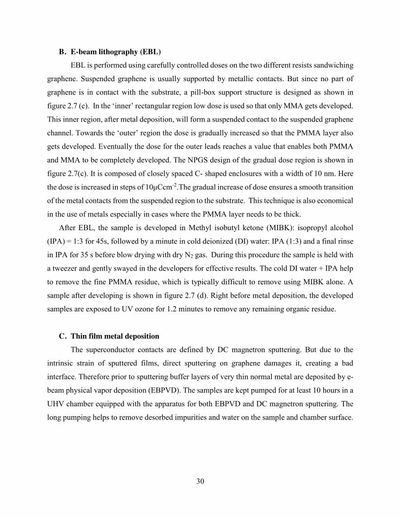
B. E-beam lithography (EBL) EBL is performed using carefully controlled doses on the two different resists sandwiching
graphene. Suspended graphene is usually supported by metallic contacts. But since no part of
graphene is in contact with the substrate, a pill-box support structure is designed as shown in
figure 2.7 (c). In the ‘inner’ rectangular region low dose is used so that only MMA gets developed.
This inner region, after metal deposition, will form a suspended contact to the suspended graphene
channel. Towards the ‘outer’ region the dose is gradually increased so that the PMMA layer also
gets developed. Eventually the dose for the outer leads reaches a value that enables both PMMA
and MMA to be completely developed. The NPGS design of the gradual dose region is shown in
figure 2.7(c). It is composed of closely spaced C- shaped enclosures with a width of 10 nm. Here
the dose is increased in steps of 10μCcm-2.The gradual increase of dose ensures a smooth transition
of the metal contacts from the suspended region to the substrate. This technique is also economical
in the use of metals especially in cases where the PMMA layer needs to be thick.
After EBL, the sample is developed in Methyl isobutyl ketone (MIBK): isopropyl alcohol
(IPA) = 1:3 for 45s, followed by a minute in cold deionized (DI) water: IPA (1:3) and a final rinse
in IPA for 35 s before blow drying with dry N2 gas. During this procedure the sample is held with
a tweezer and gently swayed in the developers for effective results. The cold DI water + IPA help
to remove the fine PMMA residue, which is typically difficult to remove using MIBK alone. A
sample after developing is shown in figure 2.7 (d). Right before metal deposition, the developed
samples are exposed to UV ozone for 1.2 minutes to remove any remaining organic residue.
C. Thin film metal deposition The superconductor contacts are defined by DC magnetron sputtering. But due to the
intrinsic strain of sputtered films, direct sputtering on graphene damages it, creating a bad
interface. Therefore prior to sputtering buffer layers of very thin normal metal are deposited by e-
beam physical vapor deposition (EBPVD). The samples are kept pumped for at least 10 hours in a
UHV chamber equipped with the apparatus for both EBPVD and DC magnetron sputtering. The
long pumping helps to remove desorbed impurities and water on the sample and chamber surface.

31
i. e-beam physical vapor deposition (EBPVD) In EBPVD, accelerated electrons hit a crucible containing the metals evaporating them.
The metal vapor rises and coats the sample directly facing the crucible at a distance.
For a good S-G interface it was found that a pressure of ~ 2x10⁻⁸ Torr or lower is required
before evaporation onto the sample. The vacuum conditions are further improved by briefly
preheating the Ti crucible an hour before deposition (with the sample facing away). This allows
for the Ti vapor to trap residual gases and seal sources of outgassing in the walls of the chamber.
When all these conditions are met, the first layer, Ti ~1.5nm is evaporated quickly followed by Pd
~1nm. Ti forms a very good sticking layer while Pd acts as a protective layer sealing Ti from any
unwanted exposure. This is especially important in the reactive sputtering of NbN, where N2 gas
is used (see next section). Each metal pocket is preheated to establish a steady base pressure and
growth rate (2A0/s) before exposing it to the sample. Slower growth rate can leave the coated metal
layers vulnerable to impurities.
ii. Sputter deposition After EBPVD, the sample is sputter deposited with the superconductor material in the same
UHV chamber. Sputter deposition is a physical vapor deposition technique where free electrons
from a negatively charged target (made of the material of interest, here Nb) ionize the gas medium
(typically Argon) in the deposition chamber. These positively ionized atoms (plasma) are
accelerated back to the negatively charged target and a cascade of collision results in atoms being
sputtered from the target surface. These atoms then get deposited on the sample facing the target.
A constant flow of the gas is maintained in the chamber during the process. In DC magnetron
sputtering used here, the magnetic field controls the sputter rate. In this thesis work, two kinds of
superconducting films were used – Nb and NbN. And in both cases a 3” circular Nb target is used.
Nb sputtering is a non-reactive process using the inert gas Ar for the plasma. NbN is reactive
sputtering where a mixture of Ar and N2 is used on the Nb target. During the sputter process the
bombarded Nb target reacts with nitrogen ions forming NbN.
A crucial challenge in sputter deposition on graphene is stress. The use of buffer metals
alone is not sufficient to protect graphene from tear or damage due to stress. To determine the type
of stress, the film is sputtered on stress free Al pre-evaporated on PMMA and lifted off in acetone
which slowly dissolves the PMMA releasing the bimetallic Nb/Al (or NbN/Al) film. This process
is observed under an optical microscope. In the case of compressive stress, the film bubble that

32
detaches forms a “flowery” or wrinkled rim as the detached film tries to increase the surface area
and minimize the elastic energy. When the film bubble breaks they curl downwards. A tensile film,
on the other hand, forms a spherical bubble with a sharp rim and when broken curls upwards (see
figure 2.8).
Figure 2.8: Stress tests for sputtered Nb films. Optical images of Nb/Al bimetallic film when lifted off in acetone from PMMA/Si substrate. a. Films with compressive stress b. Films with tensile stress c. SEM image showing a graphene channel torn apart (top) and cracks (bottom) due to stress from the sputtered film.
The stress in both reactive and non-reactive sputtered NbN and Nb depends on the flow
rate, the pressure of the gases, the sputter gun power and the distance of the sample from the target.
So to find the best combination of parameters, initially the target-sample distance and the power
were determined to give the best possible results for Tc with a reasonable contact on graphene.
Then the ‘lift off tests’ were performed by tuning the flow rate and the pressure of the gases each
time until the minimum stress condition is found. Finer tuning of the parameters is normally
required as the minimum stress values did not provide the best results on graphene. This might be
because the lift off test only shows the effective stress of the whole film. But stress can vary across
the layers. The stress of the first few deposited layers on graphene can be slightly different from

33
the results from the lift off tests. On graphene the resistance drop below Tc and the value of the
induced gap were used as gauges for the quality of the sputtered film.
Reactive sputtering for NbN: For reactive sputtering, consistent with literature, high
Ar/N2 pressure causes tensile stress while a low Ar/N2 pressure causes compressive stress [59].
The stoichiometric changes in Nb and N2 near the target can cause the intrinsic stress between each
layer of the film during sputtering. To reduce this, the flow rate of the gas mixture is increased
while adjusting the shutter valve to maintain a steady pressure. It was found that the Ti buffer layer
can also react with the Ar/N2 plasma causing bad contact resistance even at stress free sputter
conditions. To eliminate this, the Ti was covered with thin layer of Pd, as mentioned earlier. After all parameters are determined, the sputtering procedure used is as follows: After
EBPVD on sample, the chamber is partially closed from the cryopump using a shutter valve and
Argon gas is introduced into the chamber. The flow controller and the shutter valve are adjusted
so that a steady flow rate and a constant chamber pressure of 8.4 mTorr (Ar - 7.5mTorr + N2 -
0.9mTorr) is achieved. Right before sputtering on the sample, the target surface is made fresh by
pre-sputtering for 80 seconds with the sample facing away. A constant power of 470W is provided
to the Nb target at the time of sputtering. The voltage and current values typically vary from 378-
380V and 1.23-1.25A. While in operation, the pressure changes from 7.6 to 7.4mTorr indicating
the use of N2 in the reaction. This value was found to be ideal for stress free films and is often used
as a check-parameter for instabilities in chamber or target conditions. After pre-sputtering the
sample is rotated so that it faces the target. Then 70-80 nm of the superconductor at the rate of
1nm/s is sputtered. The distance between the target and the sample holder is ~10 cm.
Non -reactive sputtering for Nb: In the case of non-reactive sputtering, a similar trend in
stress is seen: high Ar pressure shows tensile stress while low Ar pressure shows compressive
stress. Here changes in Ar pressure and rate of deposition can cause the intrinsic stress. The
established procedure used in this thesis is as follows: After EBPVD, the chamber is partially
closed from the cryo-pump using a shutter valve and Ar gas is introduced into the chamber. The
flow controller and the shutter valve are adjusted so that a stable flow rate with a chamber pressure
of Ar (8.17 mTorr)) is achieved. Right before sputtering on the sample, the target surface is made
fresh by pre-sputtering for 80 seconds with the sample facing away. A constant power of 400W
is provided to the 3” Nb target at the time of sputtering. The voltage and current values typically
vary from 321-326V and 1.19-1.24A. While in proper operation the pressure is stable varying by

34
only by 0.025mTorr. If the change of pressure during growth exceeds 0.05 mTorr, it results in
intrinsic strain and poor transparency of the contacts. After pre-sputtering the sample is rotated so
that it faces the target and 60-65 nm of the superconductor at the rate of 1nm/s was deposited. The
distance between the target and the sample holder during sputtering is ~10 cm.
D. Lift-off After sputtering the sample is unloaded from the chamber. A small scratch is made on the
corner of the substrate to expose Si for gate wire bonding before liftoff2. For the lift off process,
the sample is immersed in warm acetone (700C). The acetone dissolves the resist layers lifting off
the metals with it. During the first 30s of lift off, the sample is swayed gently in the solvent so
that the detached metal films do not have a chance to stick back onto the substrate. After 10 minutes
the sample is quickly transferred to a fresh batch of acetone and kept covered for 10-15 minutes at
the same temperature. This ensures a more thorough removal of the resist layers. (Note: At this
stage the graphene is now suspended in acetone. So from here on, when handling the substrate,
utmost care is taken to avoid collapse of graphene static charges. Also the substrate should not be
directly taken out to air. This is because change in surface tension will force the suspended
graphene to collapse). Next, acetone is diluted with IPA and then the sample is quickly transferred
to a fresh beaker of pure IPA and kept for 10 minutes. To take the sample safely out to air, a beaker
of IPA is boiled on a hotplate until bubbles emerge and then is allowed to cool briefly for ~`10-15
s. Once the IPA is ~800C (and not boiling!), the sample is quickly transferred and gently stirred
for 5s to equilibrate with IPA temperature. Then it is taken out and held vertically to dry3. Since
warm IPA has a reduced surface tension and dries off quickly, this method serves as an effective
substitute to critical point drying. Hexane is also used at times as a substitute to IPA. The advantage
with hexane is the boiling point is lower (680C) and therefore the sample does not have to undergo
a huge thermal gradient. The SEM image of a sample after liftoff is shown in figure 2.7(f).
2 This process may induce momentary electrostatic charges on the substrate and if graphene is already suspended electrostatic force may force it to collapse. So as a precaution this is done before liftoff. 3 Note: IPA should vaporize immediately and the surface should be dry within a couple of seconds. Any IPA trapped in the tweezers should be allowed to dry thoroughly or should be wiped off carefully so that it does not get on to the sample

35
2.2.2. Non-suspended superconductor- graphene devices
For non-suspended sample there are only a few differences in the procedure. PMMA A4
at 3000 rpm is the only resist used. EBL is straightforward with a single dose of 420 µC/cm2. The
sample is developed for 2 minutes in cold water: IPA (1:3) and then rinsed in IPA for 35 s before
blow drying in dry N2. Metal leads are made of Ti (2nm), Pd (1.5nm) and the superconducting
film (~40 nm).
2.3. Measurement setup and techniques
Although a variety of different instruments and setups were used over the course of this
dissertation work a few of the most commonly used instruments and measurement setups are
summarized below.
2.3.1. He-3 Insert design and operation
All the superconductor-graphene devices presented in this thesis are measured in a home
built He-3 refrigerator placed in the Variable Temperature insert (VTI) space of the Oxford
superconducting magnet Dewar. The He-3 refrigerator is designed without a 1 K plot as seen in
figure 2.8. So to achieve sub Kelvin temperatures, first the He-3 gas stored in a can at the top of
the insert is completely condensed, at a stable temperature of 1.5K, into the He-3 pot located right
above the sample. The stable temperature of 1.5 K is maintained by controlled pump-flow of He-
4 gas through a capillary in the VTI space of the Oxford superconducting magnet Dewar. This
process plays the role of the 1-K plot. During this condensing process, the sorb is heated at 40 K
to release any trapped He-3 gas and ensure complete condensation. Sorb heat and temperature is
provided by CryoCon 22 Temperature controller. After sufficient time (~ 45min) is allowed to
condense the entire He-3 gas in the condenser, the sorb heater is switched off. Once the sorb
reaches a temperature of 1.5K it pumps on the He-3 cooling the He-3 pot and sample further down
to 300mK. Baffles are deployed to isolate the He-3 pot and sample from high temperature
elements. Stainless steel tubes are used for the pumping lines. The sample sits in vacuum in good
thermal contact with the He-3 pot but is sealed off from the He-4 bath by a brass can. A common
problem encountered in the design is super-leak. This may be due to minute imperfections when

36
machining the conical seal of the brass can. Various greases like Apiezon N and Bluestar CAF 1
red silicone elastomer were used to reduce the leak but a redesign of the seal is necessary for long
term operation.
Figure 2.9: Components of the bottom end of the He-3 insert.
2.3.2. Measurement setup
Figure 2.10: The typical setup used for low temperature measurement of differential resistance as a function of Vbias at different gate voltages.

37
i. For differential resistance measurements the device is ramped with a DC current riding on
a small AC current (10 or 20 nA) at a frequency of 47Hz. The output signals from the
sample is amplified using a SIM 900 scaling amplifier. The SR 830 lock in amplifier
measures the voltage response to the AC current modulation that is used to calculate the
differential resistance (dV/dI). The DC bias voltage across the source and drain leads (Vbias)
is measured using a Keithley 2001 Voltmeter.
ii. The gate voltage is supplied by a Keithley 2400 voltage source.
iii. For superconductor DC IV measurements Keithley 6221 current source and Keithley 2001
voltmeter are used.
iv. Filters – Two stage cryogenic RC filters with a cutoff frequency of ~ 3 kHz are used close
to the sample (on the sample holder as shown in figure 2.9). On the outside, at room
temperature, EMI π filters and ferrite bead filters in series with RF chokes4 are used.
2.3.3. Current annealing of suspended devices
Immediately after fabrication, suspended graphene almost always has some e-beam resist
impurities that cannot be completely removed by solvents like acetone or resist strippers like
NanoTM Remover PG. Even very small amount of solvents and water can dope graphene. This
prevents from observing the expected ballistic properties To remove such impurities the graphene
channel is heated by passing a huge current through the device[60]. The heat desorbs the impurities
in the channel. The technique works effectively for suspended graphene compared to graphene on
SiO2 since both sides of suspended sheet are free to desorb and there are no trapped impurities or
heat dissipation through the substrate. Current annealing can heat the center of the suspended
graphene strip to almost 6000C or above [11, 12]. Generally, for the suspended samples described
in the thesis current annealing is performed at 10K either in He gas flow or in vacuum environment.
But for superconducting junctions current annealing in a vacuum environment, below Tc, produced
the best results. Gate voltage Vg is kept at zero.
4 The ferrite bead high frequency filters are built following the scheme by Brain D’Urso and Jim Mac Arthur at Harvard. The link for the recipe is http://users.physics.harvard.edu/~coldwell/marcus/how_to/Ferrite_Bead_Filter.pdf

38
During the procedure, current is ramped through the sample from zero to finite values while
measuring the voltage. If a reasonable change is noticed in voltage for a fixed current, then the
current is held at that value for a while until no further changes are observed. Then its ramped back
down to zero and a gating curve is obtained to evaluate the improvement. The process is repeated
until best results (for mobility or mean free path) are obtained. The minimum current typically
required for annealing is ~0.3mA/µm. Sometimes abrupt changes in the voltage happens during
annealing due to an external impurity landing on the sample or other accidents. This can lead to
an unexpected burning of the sample. In order to prevent these abrupt the compliance of the current
source (Keithley 6221) is set to the minimum value and changed in increments when required,
while ramping the current.

39
Chapter 3
Signatures of pseudo-diffusive transport in suspended ballistic graphene superconductor junctions5
In chapter 1 it was pointed out that the conductance of a pristine sheet of graphene, away
from the Dirac point (DP), is proportional to the number of propagating modes in graphene. This
fact breaks down close to the DP where the carrier density tends to zero. Theoretical calculations
predict that pristine graphene displays unexpected “pseudo-diffusive” behavior in this regime
[14], i.e., even in the absence of defects or impurities, the transport signatures near the DP
resemble that of a diffusive conductor. The conductance should reach a universal, quantum limited
value of heS
24[61]. The origin of these phenomena is the change in the nature of transmission of
conducting channels. Near the DP, the transmission switches from propagating to evanescent
mode. In a sufficiently wide ballistic graphene, unlike in normal metals, a sizeable number of
evanescent modes can have finite transmission. At DP, these perfectly transmitting evanescent
modes gives rise to the universal conductivity and a conductance proportional to the aspect ratio.
Pseudo-diffusive behavior has been observed in 2D photonic crystals and photonic lattices
resembling graphene [62, 63]. In electronic transport a direct measurement of conductivity at DP
is difficult due to the presence of electron hole puddles, even in the best of samples. But in
graphene, the capability to tune the carrier density by using a gate electrode provides an
opportunity to observe the ‘transition’ from ballistic to evanescent mode mediated pseudo
diffusive transport. Transport signatures that are sensitive to changes in transmission of the
5 An older version of part of the work presented here is available on arXiv: 1504.06338 and is submitted for review.

40
conduction channels, like shot noise and superconducting IV characteristics, are quantities that can
be measured. Their density dependence in the ‘evanescent regime’ is expected to provide evidence
to the transition. But several prevailing technical challenges prevented observations of this
longstanding prediction.
This chapter discusses one of the first observations that indicate this transition. This was
made possible by developing superconductor proximity induced suspended ballistic graphene with
low potential fluctuations near charge neutrality point (CNP). The transition is observed when
studying the junction’s IV characteristics. When approaching the CNP (n<1010cm-2), where the
evanescent mode transport starts to dominate over the conventional propagating modes, the
multiple Andreev reflection (MAR) related features known as sub-harmonic gap structures
(SHGS) become more pronounced. The product of normal resistance and excess current, (IexcRN),
which remains constant at high carrier densities is also suppressed rapidly at low carrier densities
near the CNP. Both observations are in contrast with previous experimental observations in
disordered graphene superconductor junctions, where both SHGS and IexcRN show no significant
gate dependence. The results are in qualitative agreement with the theoretical predictions and
provide strong evidence for pseudo-diffusive transport in ballistic graphene.
At the end of the chapter, a very fine scan of the Fermi energy (carrier density) in the
vicinity of the CNP is presented, exploring the possibility of specular Andreev reflection related
signatures.
3.1. Theoretical Background: The gate dependent transmission in pristine graphene
To understand the transition of ballistic to evanescent mode transport, Katsnelson [61] and
Tworzydlo et al.,[64] calculated the transmission in pristine graphene as a function of the gate
voltage. The derivation is summarized as follows. Consider a pristine graphene strip of width W
in contact with leads separated by length L. The graphene underneath the two leads is assumed to
be heavily doped (chemical potential µ∞) with infinite modes. Then the energy states in the two
leads can be written as 22NF qkv �rf !P where k- longitudinal momentum. For the graphene strip
in between the leads, the energy states are: 22~NF qkv �r!P , where k~ - longitudinal momentum.

41
Here µ (<<µ∞) is the gate tunable Fermi energy in graphene with µ=0 representing the DP. For
W>>L, the details of the graphene edge becomes insignificant6. Allowing the wave functions to
disappear at the graphene boundaries, y=0 and y=W, the transverse momentum can be shown to
be quantized as
)21( � n
Wqn
S (3.1)
where n=0,1,2,3 –representing the modes in the graphene. Solving the Dirac equation and
matching the solution at the leads, the transmission for each mode in graphene is given by
2
)~sin(()~cos(~~
LkiLkkkTn G�
(3.2)
with F
F
vE!
G . 22~nqk � G is real for qn<δ and imaginary for qn>δ. Therefore the number of
modes F
F
vWEN
!S� (lower order modes) the transmission are propagating and for
F
F
vWEN
!S! (higher
order modes) they are evanescent. The transmission probability as a function of qnL for different
values of the dimensionless Fermi energy F
F
vLE
! N is shown in figure 3.1. The computation here
was done for N = 1000 and W/L=9.
6 It has been shown that for W/L<4 the transmission will depend on the detail of the graphene edges- armchair or zigzag.

42
Figure 3.1: Ballistic and evanescent transport in graphene. a. Transmission as a function of qL
for various F
F
vLE
! N (from equation 3.2) and b. Conductivity (σ) vsN for a pristine graphene
device. Dotted line is the naïve ballistic prediction due to propagating modes alone. Solid line is the expected curve by using transmission from equation 3.2 and the Landauer formula from equation 3.4.
For a fixed L, as κ Æ 0 as δÆ 0, higher order modes becomes imaginary and transport is carried
by evanescent modes along with the lower order propagating modes. At the Dirac point δ=0 (EF=0)
and all the modes are evanescent. The transmission probability at Dirac point for very large N is
,..2,1,0;/cosh
1cosh
122 n
WLnqLTn S
(3.3)
This finite transmission is unlike non-relativistic charge carriers. For normal incidence i.e., when
the qLÆ0, T= 1, confirming the absence of backscattering discussed in section 1.2.27.As long as
7 This problem is identical to the inter band tunneling of relativistic fermions through a rectangular barrier (as discussed in chapter 5) with the left and right contact leads representing conduction band and the graphene representing the valence band. When the energy of the electrons are aligned close to the top of the barrier, the transport is evanescent

43
W>>L, close to the Dirac point a finite number of open evanescent channels exist and the
conductance is calculated using the Landauer formula for
LWT
heG
N
nn 0
1
0
24 Vo¦ �
(3.4)
where heS
V2
04
is the quantum limited minimum conductivity. The conductance near Dirac point
is dependent on sample dimensions as in diffusive metals. The fluctuations in electrical current
(shot noise) near the evanescent regime are found to be enhanced with the gate dependent Fano
factor
¦
¦ � �
�
1
0
1
0)1(
N
nn
N
nnn
T
TTF (3.5)
reaching 1/3 at Dirac point, another similarity with the transmission statistics in diffusive metals.
This finite noise at Dirac point, without impurities or defects, is associated with the Zitterbewegung
of ultra-relativistic Dirac particles[61].
3.2. Proposals and requirements for experimental observations of pseudo-diffusive electronic transport
Several longstanding theoretical proposals have been made as to how the pseudo-diffusive
behavior can be observed in ballistic graphene devices. For this purpose, transport characteristics
that are sensitive to the nature and distribution of charge transmission in the conduction channels
should be considered. One straightforward way is to measure the shot noise and see how the Fano
factor changes with the carrier density. At higher carrier densities the Fano factor is low (~0.1) as
and at Dirac point, pseudospin conservation makes the T=1. [58] C.W.J. Beenakker, Andreev reflection and Klein tunneling in graphene, (2007) 1-20.

44
expected in ballistic transport, but when close to the evanescent regime, as mentioned earlier, the
Fano noise increases reaching the value of 1/3 at DP.
Transport in ballistic graphene (G)-superconductor (S) hybrid devices is also expected to
show pseudo-diffusive signatures [14, 15, 65]. Relevant to the work here is the prediction by
Cuevas et al.in [15]. They showed that in short ballistic SGS junctions the quasiparticle current-
voltage characteristics such as excess current and SHGS amplitudes should display a strong Fermi
energy or carrier density dependence near Dirac point, reflecting the crossover from ballistic to
pseudo-diffusive charge transmission. Previous (experimental and theoretical) work using
superconductor point contact break-junctions (S-S, S-Insulator-S etc.,) have confirmed the
sensitivity of SHGS amplitudes to individual transmission of the channels in the point contact. In
the experimental work the number of channels and their transmission were controlled by adjusting
(breaking) the contact[66]. But here, in graphene, by using a gate electrode to tune the Fermi
energy we can control the number of channels and their transmission into the evanescent regime.
This leads to a direct insight of an intrinsic property of graphene’s energy spectrum!
In realizing these predictions, the experimental work carried out so far [18-20, 67, 68], has
been impeded by numerous technical challenges. To reach the energy scale required for evanescent
transmission, the Fermi wavelength F
FF E
hv O should approach the dimensions of the sample.
Here m/s is the energy independent Fermi velocity and EF is the Fermi energy. Therefore
the potential fluctuations (δEs) near CNP should be small, a few meVs, even for a sub-micrometer
long channel. In addition, charge carrier scattering should largely be eliminated, so that the
transmission of the carriers reflects the intrinsic nature of the transverse modes. This requires the
devices to be ballistic. Due to the strong substrate-associated disorder, previous observations were
marred by the presence of large potential fluctuations and short mean free path (usually <<100
nm) due to the SiO2 substrate (see section 1.3.3). More recently, graphene/h-BN hetero-structures
have demonstrated ballistic transport [69]. Josephson current has also been observed in these
structures when coupled with superconductors [23, 24]. However, with these methods achieving
both very low carrier density and highly transparent S-G interfaces is still under development.
610|Fv

45
3.3. Experimental methods and sample characterization
In order to meet the requirements to explore the pseudo-diffusive regime near DP the
fabrication method as explained in Chapter 2 was developed. Here the important details are
presented. The graphene was deposited using mechanically exfoliated highly oriented pyrolytic
graphite (HOPG). The graphene channel was designed to have a large aspect ratio (W/L) ~9 with
width W =5.5μm and length L = 0.6μm. Such geometry minimizes any effect from the edges of
graphene and complies with the theoretical prescription 4/ tLW [64]. Moreover, a larger W/L
improves experimental observation by allowing more evanescent modes (large higher order N) to
contribute to the conductance. To suspend graphene an etch-free method as outlined in chapter 2
and previous work is used[70]. The contacts were formed by electron beam evaporation of Ti and
Pd to form a thin buffer layer ~2nm followed by DC magnetron sputtering of ~60 nm Niobium
(Tc~9K, Hc2~3.5 T). The Ti/Pd buffer layer helps in achieving a low contact resistance. The
sputter conditions and device geometry are determined to minimize the stress on graphene. This is
essential for a transparent superconductor- graphene interface and also improves the chances of
getting a ballistic graphene channel by current annealing. All the measurements were performed
in an Oxford Instruments VTI refrigerator and the He-3 insert (see Chapter 2, section 2.3), with
room temperature ferrite and π-filters, and cryogenic 2-stage RC filters
The gating curves of the device after current annealing measured for two different
temperatures, 9K (~ Tc) and 1.5 K, are presented in figure 3.2(b). At T~9K the device shows a
maximum mobility of >250,000 cm2/Vs and the mean free path is sample length limited. From the
smear at the CNP and using QH measurements (see below) to establish the relation between n and
Vg (see below), the minimum carrier density is 9104.1~ usn cm-2. This corresponds to a potential
fluctuation δES~ 4.4meV at CNP, the smallest value observed so far in such devices. To
characterize the Fermi wavelength, similar to Ref.[15], a dimensionless parameter
is used. Therefore the maximum δES~ 4.4meV in our sample corresponds to κ~4.0. The resistivity
at CNP is . The small discrepancy from the theoretical value of may be
attributed to the presence of electron hole puddles and finite Coulomb scattering which in practice
cannot be completely avoided. The excellent quality of the device is also evident from the QH
FF
F Lv
LEOSN 2
!
2493.019~
ehk S
: 24ehS

46
measurements. As shown in figure 3.2(c), at T=1.5K, and in a low magnetic field of B= 300mT,
pronounced magneto-oscillations are already observed. At B=500mT, the sample displays fully
developed anomalous QH plateaus at the expected filling factors ν= ,...6,2 rr for monolayer
graphene. From these QH plateaus, the carrier density (n)-gate voltage (Vg) relation is found to be:
� � 210 cm [Volt] 1084.1 ��uu NPg VVn where V9.0� NPV is the gate voltage at CNP. This is
consistent with the estimation using the geometrical capacitance considering 285nm SiO2 in series
with 220nm (thickness of the PMMA spacer) of vacuum. On the higher mobility electron side,
additional oscillatory features in resistance, R (Vg), at ...8,4,1ν= , etc. are observed which may be
attributed to the onset of broken symmetry. The resistance at the CNP displays diverging behavior
with increasing field, starting at a low B~0.3T. All these observations demonstrate that the sample
is of extremely high quality, with long mean free path and minimal potential fluctuations.
Next, we study the superconducting proximity effect at T=1.5K in the absence of magnetic
field. Compared to T>TC, the junction resistance is significantly reduced. For VV CNPg V3.0!� ,
the resistance vanishes reflecting the presence of a finite supercurrent. Figure 3.2(d) shows the
differential resistance dIdV as a function of bias voltage (Vbias) taken at V5.7 � CNPg VV (κ~39).
From the curve we obtain the superconducting gap on graphene (Δ) ~0.34meV. This value is
significantly smaller than the BCS gap of Nb, � � meVBCS 37.1~764.1~0 cBTk' , and varies slightly
from sample to sample. Similar reduction has also been observed in superconductor-nanowire
weak links [71, 72] and can be attributed to the impact of the finite-thickness of Ti/Pd buffer layer.
At finite '�� 2biasV , the resistance drops down to ~ 40% of the normal resistance (RN) due to
superconducting proximity effect. Evaluating the value of the normalized excess current /e~mV4.0~ 'Nexc RI and using the OTBK model [57] we estimate the dimensionless barrier
strength of the interface, Z ~0.5. The SHGS are very weak, consistent with the theoretical
prediction for ballistic channels with high transmission [73, 74]. Other factors that may affect the
weak SHGS include the small induced superconducting gap and the relatively high measurement
temperature.

47
Figure 3. 2: Device characteristics: a. Main panel: Device schematics. Inset: SEM Image of the device. Scale bar is 2μm. The graphene channel is highlighted by the open rectangle b. Resistivity in units of (πh/4e2) as a function of gate voltage (Vg) at T=9K (blue) and T (<TC) =1.5K (red). c. QH measurements: Conductance versus filling factor for two different magnetic fields 300mT (blue) and 500mT (red) at T=1.5K. d. Differential resistance as a function of bias voltage (Vbias) at T=1.5K. Gate voltage is 7.5V away from the CNP gate voltage (VCNP). The corresponding κ ~39(see text) and the induced gap (Δ) =0.34meV.
Now we focus on the behavior of the differential resistance as we approach the CNP. Figure
3.3 (a) shows the normalized differential resistance dIdV
RN
1 as a function of Vbias obtained at
various gate voltages. When V6.0�� CNPg VV ( 210 cm10 ��n and 9�N ), the differential resistance
curve starts to develop a pronounced dip at mV68.0~/2 eVbias ' . As the Vg is ramped further
towards the CNP, i.e., for V3.0�� CNPg VV ( 29 cm107.5 �u�n and 5.5�N ), while the dip at
eVbias /2' continues to be deeper, other SHGS start to emerge at low Vbias. All the observed
T=1.5K

48
features appear at neVbias /2'r where n=1, 2, 3… as expected for MAR processes and their
positions in Vbias are independent of Vg. The higher order features are within noise. The observed
features are sharpest at CNP where the SHGS at n=1, 2 and 3 are all easily resolvable. But once
Vg is ramped to the hole side, slightly away from the CNP (ĸ~ -1.9), the SHGS begin to weaken.
The dip at n=1 shows the most prominent response to the gate voltage. In conjunction with the
appearance of the pronounced SHGS, the overall shape of the normalized differential resistance
curve transforms from a “V”-shape to a shallow profile. We note that the observed gate-
dependence of the dIdV versus biasV curves is specific to superconductivity. Above Tc the
“background” dIdV versus biasV , within the bias voltage range studied here, shows roughly no
curvature.
Figure 3.3: Normalized differential resistance dIdV
RN
1versus bias Voltage (Vbias) for different
F
F
vLE
! N . Individual curves are shifted for clarity. Dotted lines indicate SHGS. a. Ballistic SGS:
Ti/Pd/Nb contacts at T=1.5K. Evolving SHGS at Vbias=±2Δ/ne for n=1, 2 and 3 where 2Δ=0.68meV.b. Diffusive SGS: Ti/Pd/Nb contacts at T=1.5K. Unchanged Gap feature at Vbias=±2Δ/e=±0.3mV.

49
For comparison, we present a similar set of data for diffusive samples with Ti/Pd/Nb
(Figure 3.2 (b)) contacts. In the diffusive case, graphene channel sits on SiO2 and has a mean free
path Llm �� and meV40~FEG . In contrast to the ballistic sample, there is no significant gate
voltage dependence of the SHGS disordered devices for a large range in κ. The results are no
different from previous work on diffusive graphene samples with Ti/Al-contacts (see [20]). We
note that the higher order SHGS are unresolvable in the diffusive Ti/Pd/Nb device, which may be
attributed to the smaller induced superconducting gap and the relatively high measurement
temperature.
To understand the observed gate-dependent SHGS, we consider the Fermi energy
modulation of charge transmission in a ballistic graphene device in figure 3.1. In general, the
transmission of Dirac electrons in graphene can be described by a summation of contributions from
the boundary-defined transverse modes, each satisfying the Dirac-Weyl equation. At high
densities, the channels in the ballistic graphene strip are propagating with high transmission.
Approaching the CNP, however, the propagating modes become suppressed and the evanescent
modes contribute increasingly to the conduction with more channels having a lower transmission.
With superconducting contacts, it has been shown that the oscillatory amplitude of the SHGS
increases due to the contribution from the low-transmitting channels [15, 73]. As a result, close to
the CNP where evanescent modes with low transmitting probability dominate, the SHGS are more
pronounced than at large gate voltages. The stronger gate-dependence of lower order SHGS,
especially n=1, is also consistent with the theory. This is because compared to the higher order
SHGS, the lower order ones are formed by Andreev quasi-particles that traverse the graphene
channel fewer times and hence involves more contribution from the low transmitting channels.

50
Figure 3.4: Normalized Excess current (IexcRN) as a function of F
F
vLE
! N a. Experimental
data: IexcRN is calculated from the current-voltage characteristics of the device for different Vg at 1.5K.The (blue) line is drawn as a guide to the eye. b. Theoretical calculation: for short ballistic SGS junction with W=5.5μm and L=0.6μm at T=0K.
A quantitative comparison with the theoretical predictions for pseudo-diffusive transport
can be made by characterizing the excess current through the SGS device. Generally in a SNS
junction when eVbias>>2Δ, the current though the sample consists of a normal ‘Ohmic’ current (IN)
and an ‘excess’ current (Iexc) due to the superconducting proximity effect. Compared to the
Josephson current, excess current is much more robust against the influence of the electromagnetic
environment, and hence provides a reliable parameter for characterizing the proximity effect. In
SGS junctions the abundance of nearly ballistic modes at large Fermi energies leads to large excess
current. However, in the vicinity of the CNP the number of highly transmitting propagating modes
decreases and the charge transport becomes increasingly evanescent thereby decreasing the excess
current. Figure 3.4 (a) shows the normalized excess current IexcRN in our device (extracted from
current-voltage curves at various gate voltages) as a function of κ. For κ >9, i.e., in the ballistic
transport regime IexcRN ~0.4mV~1.2Δ/e whereas for κ <9, there is a clear gate dependence. The
excess current sharply reduces when approaching the CNP. This reduction coincides with the onset
of the enhanced SHGS as shown in figure 3.3 (a). For short ( '!LvF! ) ballistic graphene Josephson

51
junctions, the transmission dependence of the excess current been theoretically studied in reference
[15]. With L=0.6μm, meVLvF 1~!
and since the induced gap meV34.0~' our device
marginally satisfies the short junction limit. The observed gate modulation of normalized excess
current is in qualitative agreement with the zero temperature theoretical calculation as shown in
Figure 3.4 (b). Using W=5.5μm and L=0.6μm of our sample and following the result in [15], the
total excess current in a short Josephson junction is calculated as a sum of its individual
contribution from all the transverse modes, each determined by the corresponding transmission
coefficient Tn.
� �¦ ¸¸
¹
·
¨¨
©
§¸¸¹
·¨¨©
§
��
��
���
�'
n n
n
nn
n
n
nexc T
TTT
TT
TheI
1111
ln122
11
2 22
(3.6)
The discrepancy between the theory and our observation, especially in the values for normalized
excess current, may be attributed to a few factors. First, the theory assumes an ideal SN interface
(Z=0), whereas in our device Z~0.5. Secondly, our measurements were carried out at a base
temperature of ~ 1.5K while the theory does not consider a finite temperature. Both these factors
contribute to the reduction of the normalized excess current. In addition, for lowest values of κ,
the theory does not consider the presence of the electron hole puddles that exists in real devices.
These, together with temperature smearing, can we explain the slight broadening in the excess
current dip with an onset at κ~9 compared to the theory (κ~4).
An imperfect SG interface that may also result in Fermi energy modification of
transmission coefficients without any direct consequence of the Dirac fermionic nature of
graphene. Indeed it has been suggested that in graphene-metal junctions, the doping of the metal
contacts can extend into graphene, forming a p-n junction that imposes the charge carrier
reflections [75, 76]. A direct evidence of the presence of such interfacial p-n junction is the
electron-hole asymmetry in the R vs. Vg dependence. As the gate voltage is swept across the CNP,
the S-G interface changes from p-n to n-n and the asymmetry in the R vs. Vg dependence can be
associated with the transmission probability across the S-G junction. While the presence of such
junctions may affect the SHGS and Iexc, the gate voltage dependence will be gradual with no
particular energy scale. In addition, such contact-doping associated reflection should give rise to

52
asymmetry in the quasi-particle current-voltage characteristics that persists up to large gate
voltages on both the electron and hole sides[24]. These are apparently not consistent with the
observation of a sharp dip on the IexcRN vs. EF dependence for EF<8meV, and the qualitatively
symmetric behavior with respect to the CNP.
3.4. Probing specular Andreev reflection
Applying Dirac BdG equation for the S-G interface, Beenakker[13] showed that when
approaching the DP the switch from retro Andreev reflection (r-AR) to specular Andreev
reflection (s-AR) will be marked by an inversion in the bias dependence of the sub gap
conductance-(1/GN) dI/dV. The results are plotted in figure 3.5(a). The plot for EF/Δ=10 shows
the typical conductance enhancement due to r-AR when eVbias is below the gap. A contrasting
feature is seen for the s-AR curves at EF/Δ = 0.2, 0.4.., 1.4. In the s-AR regime (i.e., EF ~ Δ), when
eVbias is close to EF, there is a dip in (1/GN) dI/dV which reaches zero at eVbias=EF. This is because
when E=eVbias =EF, the reflected quasiparticle has to be at the DP (compare with illustration in
figure 2.5 in Chapter 2). This is not possible and therefore the AR probability vanishes. Figure
3.5(b) shows the 2D plot of (1/GN) dI/dV as a function of (Vbias, EF/Δ).
In experiments studying s-AR, the feature to look for is the sudden appearance of a sub gap
peak (dip) in the differential resistance (conductance) that is distinguishable from the MAR
features when EF~Δ.
With the high quality sample and low potential fluctuations at Dirac point of the order of
the gap, it is reasonable to expect signatures for specular Andreev processes to also appear in the
SGS sample presented here. In order to explore this, dIdV vs Vbias was measured by a very fine
scan in gate voltage close to the Dirac point. The 2D version of the experimental data is shown in
figure 3.6. Each curve that make up this plot is measured at gate voltage increments of 0.005V (Δn
=9.2 x 10⁻⁷ cm-2). For the sample area of 2.5µm2, the number of electrons in graphene changes
from 100 to 40 and each gate measurement adds 2 electrons. In the low bias regime, when
EF<2.7meV, (in the range of 0≤Vg-VCNP≤0.02V) an anomalous peak emerges. This peak cannot
be associated with those accompanying higher MAR processes. So there is a possibility that the
peak might be related to the onset of s-ARs.

53
There are several factors that need to be considered in confirming this claim. For example,
the gap 2Δ =0.67meV is smaller than the EF values for which the peak is observed. The peak is
weak for Vg> 0.02V and there is no clear sign of it moving out towards higher bias, like in the
theoretical plot 3.5(b). But the theoretical calculations are for SG devices and the devices measured
here are SGS samples. So finite interference from MAR processes cannot be excluded. The thermal
smearing of EF/Δ for T=1.5K will also play a role in this energy regime. Also the plots in figure
3.5, based on [13], assume a step like pair potential at the SG interface. This is not the case in real
devices. More theoretical calculations for SGS junctions, accounting for a smoother change in pair
potential across the interface and MARs is required to make a clear comparison of the observations.
Figure 3.5: Differential conductance curves for specular Andreev reflection at a superconductor-graphene junction –Plots based on theoretical calculations in [13] for T=0K: a. Contrast between differential conductance for specular and retro Andreev reflections: Green curve (EF/Δ=10) represents retro. For EF/Δ≤1, the curve flips due to specular Andreev reflection. b. Differential conductance vs. Vbias and EF.

54
Figure 3.6: Differential resistance vs. Vbias for EF≤5 meV at T=1.5K. Below the white dotted line additional peaks appear at low bias (indicated by red arrows). This does not follow the harmonics of MAR dip-peak structures (indicated by black arrows).

55
Chapter 4
Magneto transport in type II superconductor –graphene Josephson weak links 4.1. Introduction and motivation
Long before the discovery of graphene, it has been predicted that a proximity induced
2DEG system under a magnetic field can show unconventional QH plateaus due to the presence
of Andreev bound states at the Superconductor-Normal (SN) interface[22]. These predictions
hitherto remain unconfirmed. The ability to fabricate ballistic Superconductor-Graphene (SG)
devices as seen in the last chapter and several other advances in fabrication of ballistic graphene
devices[50] adds a new dimension to this research with interesting possibilities that may arise
when merging ultra-relativistic physics with superconductivity. Induced superconductivity in the
chiral edge states in graphene can also be used to detect valley polarization[17]. Also, more
recently, it has been predicted that s –wave proximity induced superconducting low dimensional
materials with large spin orbit coupling (SOC) and Zeeman split energy spectrum can host
Majorana bound states [77]. Although graphene has a weak SOC, recent advances in fabrication
has increased hope in engineering devices that can support spin polarized edge states. These edge
states when coupled with a superconductor can form topological superconductors for observing
Majorana modes and even other exotic non-abelian states in the fractional QH regime[16].
Several experiments have been reported in the last decade that studied induced
superconductivity in the QH regime, but still a ‘clear’ evidence for the existence of Andreev edge
states and enhanced QH conductance plateaus is lacking [23, 78-80]. In these experimental work
type II superconductors are used as they have higher upper critical fields. Although the reasons are
not clear at this stage, one of the common features in type II Superconductor hybrid devices with
thin buffer normal metal layers between the S and N (like Ti, Pd in the previous chapter) is the

56
presence of a reduced superconducting gap. This can be due to the reverse proximity effect near
the superconductor or minigap in N due to the presence of Andreev bound states. In AR, since the
incident/reflected quasiparticles follow the same trajectory on the normal side of the interface and
do not enclose a flux, they are immune to any phase breaking effect by magnetic fields. But an
interesting situation was proposed to occur [81, 82] due to screening currents that form in the
superconductor in a magnetic field. Screening currents are composed of a moving Cooper pair
condensate. At the SN interface, in order to accommodate this Cooper pair momentum on the S-
side, the incident and Andreev-reflected quasiparticles acquire a momentum shift. When the
applied magnetic field is sufficient that the associated energy shift is comparable to the
superconducting gap at the SN interface, AR probability becomes significantly suppressed, thereby
weakening the proximity enhanced conductance. This so called “Doppler shift” effect is significant
when the effective superconducting gap near the SN interface is small. Experimentally, the effect
of screening currents on proximity-induced superconductivity has been studied in Niobium/2DEG
junctions [83]. Here, at fields of ~ 200mT, the AR probability is completely suppressed. The
suppression was accounted for by considering the effect of diamagnetic Meissner currents in the
superconducting leads.
But in thin film superconductors vortex currents are more dominant than Meissner
current[84] . The arrangement of vortices is highly dependent on how the field is introduced and
ramped through the superconductor. But so far no experimental work has studied the impact of
vortices and their distribution on the proximity effect. In this chapter, magneto transport in NbN
superconductor - non suspended graphene weak links is presented, where the role of the vortices
on the suppression of the proximity effect is revealed. This is achieved by employing a variety of
magnetic field ramping techniques and studying their effect on the SGS IV characteristics. Using
these techniques the suppressed proximity effect is retrieved at magnetic fields, where QH edge
states are expected to emerge in ballistic graphene (500mT-1T). At the end of the chapter, a
possible qualitative explanation of these observations is presented within the Doppler-shift
framework.

57
4.2. Device fabrication and characteristics
This chapter deals mainly with non-suspended graphene Josephson weak links. The details
of the device fabrication is presented in detail in Chapter 2. For the sake of continuity, some of the
important aspects of the fabrication procedure is presented here in short.
Graphene-superconductor weak links (SGS) are fabricated on SiO2/Si substrates, through
standard mechanical exfoliation and e-beam lithography. For a highly transparent S-G interface, a
buffer layer of Ti (2nm)/Pd (1.5nm) is thermally (e-beam) evaporated onto the contact area in a
UHV environment (base pressure ~2 x10⁻⁸ Torr). Immediately after the evaporation and without
breaking vacuum, superconductor NbN is deposited onto the samples via DC magnetron
sputtering. This reactive DC Magnetron sputtering is carried out in N2/Ar environment. The buffer
layers are essential to protect graphene from damage during sputtering and reduce the contact
resistance of the interface. The sputter conditions and the lead geometry are chosen to minimize
the stress on graphene. The current and voltage pair leads are split close to the contact point on the
graphene channel to minimize the contribution of contact resistance especially above TC. Typical
graphene channels are of L~0.5μm in length and W~1.5-10 μm in width as shown in figure 4.1(a)
and 4.2 - left inset. All devices are measured in a He-3 refrigerator, equipped with room
temperature EMI ferrite beads and π-filters, and cryogenic 2-stage RC filters. The mobility of the
graphene channel is estimated to be 5000-6000cm2/Vs from gating of the two-terminal resistance
(Figure 4.1(c) just below the transition temperature of the NbN leads (Tc ~ 11K) and the mean free
path is calculated to be ~ 50-60nm. The zero-bias resistance below Tc, drops rapidly with
decreasing temperature and reaches zero at T~1-2K, and the IV curves at T=0.4K in Figure 4.1(b)
clearly show the existence of critical current IC~75nA . In some of the wider samples which show
large IC ~1uA (Figure 4.2 right inset) at sub-kelvin temperatures a very sharp, equally spaced
oscillations in the differential resistance (dV/dI) vs bias voltage (Vbias) is observed. This might be
due to self–induced Shapiro steps (Figure 4.2) and has been also observed in other
experiments[85]. All these features demonstrate a transparent S-G interface.

58
Figure 4. 1: Properties of non-suspended NbN-graphene Josephson weak link a. SEM image of the device. The graphene channel is highlighted. Scale bar is 1 μm. b. Resistance (R) vs. temperature of the SGS junction showing Tc=11K. c. Gating curves R vs Vg at 5K and 110K. d. Current Voltage (IV) charactersitcs of the junction at 0.4K. The switching to critical current IC is ~ 75nA. T~0.4K.

59
Figure 4. 2: Differential resistance (dV/dI) vs bias voltage (Vbias) of a 10 μm wide graphene- NbN Josephson junction. (left inset) SEM image of the device. Scale bar is 2μm. (right inset) Current-Voltage (IV) characteristics showing Ic~ 1uA. T~0.4K.
At T=0.4K, a clear evidence of multiple ARs (MARs) in dV/dI vs. Vbias curves is seen, as
shown in figure 4.3. Here a conductance enhancement is observed when bias voltage is less than
~1.5mV. At lower bias voltages sub-harmonic gap structures are observed, where the valleys of
the oscillations agree well with the expected MARs at 𝑉𝑏𝑖𝑎𝑠 = 2𝛥𝑛𝑒
, with Δ=0.15meV (figure 4.3
bottom right). As in the last chapter, the gap Δ at the metal-graphene interface is sample dependent
but is always much less than the bulk gap of NbN (from BCS theory Δ(0)=1.764*kBTc~1.8 meV
for 11K).

60
Figure 4.3: Multiple Andreev reflections in NbN-graphene Josephson weak links. (left) Differential resistance (dV/dI) vs bias voltage (Vbias) at T=1.5K (top right) Plot zoomed in to show MAR related resistance dips at Vbias=2Δ/ne (bottom right) Vbias -MAR dips vs 1/N where N-integer with a linear fit to extract the gap 2Δ=0.294meV.
4.3. Magnetic field measurements
For the magnetic field measurements first, the typical zero-field-cool (ZFC) procedure is
used where the sample is cooled below Tc and then the magnetic field B is monotonically ramped
up to the desired values. The data presented here is taken at a gate voltage of 10V from the Dirac
point. For each B, the bias dependence of the differential resistance is measured. The ZFC- ramp
up dV/dI normalized by the normal resistance (RN) of the junction slightly below Tc. (1/RN) (dV/dI)
vs Vbias is shown in figure 4.4. The measurements are performed at a stable temperature of T=1.5K.
For B=0, RN drops by 25% at Vbias=2Δ. Since both supercurrent and the oscillatory MARs features
become completely suppressed under a very small magnetic field of ~1mT, the SGS junction can

61
be treated as two separate SG junctions with single AR at the interface. Further increasing the
magnetic field, the AR enhancement of conductivity is rapidly suppressed and eventually vanishes
around B=200mT. Above 200mT the dV/dI remains flat at RN.
-2.0 -1.5 -1.0 -0.5 0.0 0.5 1.0 1.5 2.0
0.6
0.7
0.8
0.9
1.0
1/R
N(d
V/d
I)
Vbias(mV)
1000 700 200 100 80 60 40 30 20 15 10 8 5 0
B(mT)
T=1.5K
Vg=20V(~10V from charge neutrality point)
Figure 4.4: Zero field cool differential resistance measurements. Measurements are taken by monotonically increasing field from 0 to 1T at T=1.5K. Vg=20V, 10V from the charge neutrality point.
The effect of B on single ARs at the S-G interface can be better evaluated by calculating
the excess current Iexc. The normalized excess current (IexcRN) vs B is shown in figure 4.5(a) and
it is clear that the excess current drops quickly and eventually reaches and remains zero above B=
200mT. A similar rapid suppression of the AR conductance enhancement at low magnetic fields
is also seen in the Nb-graphene devices figure 4.5(b) at the same temperature and gate voltage
except that the suppression is not complete and there remains a small non-zero excess current at

62
the higher end of the applied field range. The suppression, however, irrespective of the
superconductor does not change with carrier density or with temperature below TC. Also in the
field range measured the NbN and Nb do not lose their superconductivity (verified to ~ 5T and
Hc2 of the Nb films ~ 3.5T). Only the proximity effect is suppressed.
0 50 100 150 2000
20
40
60
80
100
120
140
Niobium Nitride sample ZFC- Ramp Up@ 1.5K
I excR
N(P
V)
B(mT)0 100 200 300 400 500
20
40
60
80
100
120
140
Niobium sample ZFC- Ramp Up@ 1.5K
I excR
N(P
V)
B (mT)
Figure 4.5: IexcRN vs. applied magnetic field (B) for zero field cool- ramp up measurements: for (a) graphene - Nb (b) graphene-NbN junctions at 1.5K.
To explore the possible impact of magnetic flux (vortex) distribution on AR, the
differential resistance measurements are taken under two other conditions. One is the field-cool
(FC) process, where each time the magnetic field is applied above Tc and then device is cooled
down to T=1.5K; while in the “zero field cool down-ramping” (ZFC ramp down) process, the
magnetic field is ramped up from zero below Tc first to a high value (>1T) then decreased down
to the desired values. The schematic of the three field ramp processes is shown in figure 4.6.

63
Figure 4.6: Schematics of the three magnetic field ramping procedures - 1. Zero Field Cool (ZFC) ramp up 2. ZFC- ramp Down 3. Field Cool (FC).
The 1/RN (dV/dI) vs Vbias at 200 mT for all three methods is shown in figure 4.7. The
conductance enhancement is retrieved when using the FC method whereas an even larger
enhancement is observed by the ZFC ramp-down method. The differential resistance is also
measured for various other values of B, in the range 0 to 1T. IexcRN is a good estimate of the strength
of the single AR probability. Therefore the IexcRN values is obtained from the differential resistance
curves and is shown as a function of the applied field B in figure 4.8. It is now clear that, in general,
the excess current is higher for the FC technique compared to the ZFC ramp up technique. For the
ZFC-ramp down technique the excess current is the highest compared to the other two methods
for fields above ~40mT. However, below 40 mT, the excess current dips slightly. This means that
while the S-G interface is below Tc, cycling the field through it from zero to 1T and then back to
zero does not retrieve the supercurrent. It is also important to note that the excess current obtained
by the field cool technique overlaps with the ZFC ramp up data in the low field range (0-10 mT).

64
-2.0 -1.0 0.0 1.0 2.00.88
0.90
0.92
0.94
0.96
0.98
1.00
1/R
N(d
V/d
I)
Vbias(mV)
ZFC Ramp up ZFC Ramp down FC
T=1.5K
Figure 4.7: Comparison of the differential resistance curves at B=200mT for the three magnetic field ramping procedures. ZFC (blue), ZFC-Ramp down (red) and FC (green) and T=1.5K.
0 200 400 600 800 10000
50
100
150
200
250 ZFC RampDown FC Ramp Down ZFCRamp Up
2Iex
cRN(P
V)
B(mT)
Figure 4.8: Comparison of excess current vs applied field B for the three field ramp procedures. ZFC (blue), ZFC-Ramp down (red) and FC (green) at T=1.5K.

65
4.4. Discussion and future work
The ZFC measurement on the suppression of AR probability in presence of a small
magnetic field in our devices is qualitatively consistent with the previous theoretical and
experimental works on superconductor/2DEG systems [83]. In these devices the “Doppler” shift
of the quasiparticle spectrum was explained considering the Meissner current. At the SN interface
on the S side, the Meissner current can be considered as a moving Cooper pair condensate with a
momentum (2ps). Here Aeps&&
where A&
is the vector potential. The presence of this current shifts
the momentum of the incoming and reflected Andreev electron (p) and hole (-p) on the N-side to
p+ps and –p+ps respectively (in the direction of the current). If the resulting energy shift
Fsvp H~ in the quasiparticle excitation spectrum is greater than the reduced gap (Δ)8 the Fermi
energy of the quasiparticles shifts outside the proximity reduced gap. This suppresses the AR
probability [81, 82].
In type II superconductors vortices enter the superconductor above the lower critical field
(Hc1) << upper critical field (Hc2). In narrow superconducting strips the Hc1 is further reduced. The
vortices form once the magnetic field is above20~
cm L
B ) , where eh 2/0 ) is the superconducting
flux quantum and Lc is the width of the superconducting thin film[84]. For the dimensions of our
devices, this gives mTBm 5.0~ which is at the low end of the magnetic field applied in our
experiments. So the effect of vortices should be considered in explaining the observations. Vortices
nucleate at the surface of the superconductor and penetrate into the interior of the thin film. Each
vortex carries a flux quantum 0) in its core of size ξ -the superconducting coherence length.
Inside the core, the superconducting electron density vanishes. The field is maximum at the core
and decays over a certain length scale9 determined by the penetration depth λ. Screening currents
encircle the core in the region where the field decays. In strong pinning superconductors when a
magnetic field is applied, the motion and distribution of vortices on the superconductor is
8 Note that Δ is smaller than the bulk superconducting gap of NbN, which, from the Tc should be around 1.8meV. So the Doppler shift mechanism is observable in SN interfaces where the gap is reduced at the SN interface. 9 Length scale over which the field decays differs based on the vortex type. Pearl vortices that form in thin films decay as 1/r within the Pearl length (=2λ2/d, where d- thickness of the film) and 1/r2 outside Pearl length. The scale of Abrikosov vortices that form in bulk films is log (λ/r).

66
determined by how the field is applied and hence is different for ZFC vs. FC. It also depends on
ZFC ramp directions performed below Tc. The hysteric-like behavior of the excess current with
ZFC - ramp up and down procedures and the inability to completely retrieve the supercurrent
through the device after a complete ZFC cycle all indicate that the distribution of vortices has a
direct impact on the proximity effect. The resultant vortex screening current emerging from the
distribution should correlate to the observations of the suppression of the proximity effect in the
same manner as the Doppler shift mechanism with Meissner current.
Based on results from magneto-optic imaging of vortices reported in work [86, 87], the
following explanation for the observations is proposed. For the ZFC, above Bm = 0.5mT, the
vortices penetrate the NbN superconductor from the edges (boundaries). Due to vortex pinning,
edge defects and vortex-vortex interaction, they pile more on the edges. As the field is increased
more vortices enter from the edge and slowly nudge the other vortices to the center of the
superconductor. Eventually, above a certain field a non-uniform distribution of vortices builds up
in the entire leads. This completely suppresses the proximity effect. On the other hand in the case
of FC, above TC, the magnetic field penetrates through the superconductor uniformly and when
cooled below TC the vortices are “frozen” (pinned) in place and the distribution remains uniform.
In the case of ZFC-down ramp, while ramping down, flux free regions can form due to penetration
of anti-vortices (vortices of opposite polarity) that annihilate the vortices. These flux free regions
can explain the increase in excess current. But the annihilation is not complete due to strong
pinning and non-uniform vortex density. So when the field is ramped back to zero, some vortices
remain trapped and the proximity enhanced conductance is not fully recovered. This can explain
the dip in the excess current below ~40mT for ZFC ramp down in figure 4.8.
The actual distribution of vortices (or the associated screening current distribution) is
difficult to calculate as it depends on the pinning properties, grain boundaries, defects, film
roughness and the geometry of the leads. But the observations follow the general predictions of
the Bean’s critical state model[88] ,which explains the distribution of Abrikosov vortices in bulk
type - II superconductors with width >> λ. Theoretical calculations are required to see how the

67
model exactly applies for the arrangement of Pearl vortices in thin films of width~ λ 10 (The
superconducting leads on the sample are of width ~2μm and a rough estimate of λ for
NbN~0.5μm).
The Oxford superconducting magnet also uses the type II superconductor – Nb3Sn and it
can have trapped flux when a current is ramped back and forth through it. So it is important to
know whether any hysteresis from ramping the magnet back and forth affects the measurements.
But from tests performed using FC measurements of differential resistance, the IexcRN vs B curves
for ramp up and ramp down (figure 4.6) overlap. This eliminates the role of the magnet11 and
confirms that it is indeed the vortices in the NbN contacts that are responsible for the observed
suppression of the proximity effect. Typically trapped flux in magnet systems after a complete
ramp cycle, if present, is found to be low, with a shift in the field around 20-50 gauss.
0 100 200 300 400 500 600 700 800 900 10000
50
100
150
200
250
2Iex
cRN(P
V)
B(mT)
FC Ramp Up FC Ramp Down
Figure 4.9: IexcRN vs B - for FC ramp up and down to test any impact from trapped flux in the superconducting magnet system.
10 A possible way to study the effect of vortices and test it directly with the Bean’s critical model is to make wider, thicker leads. But the technical challenge is the total stress of the wide film on the graphene will be larger and therefore can affect the interface properties. 11 The reason for the spike around 65mT, which is seen in all curves, is unknown. But generally the excess current for FC Ramp up and down overlap especially for the field range 0-60mT, unlike the ZFC Ramp-down curve.

68
In addition to vortices as the source of the supercurrent, the impact of the current’s spatial
distribution for the overlap-type SN junctions should be considered. The presence of a distributed
contact resistance and graphene’s sheet resistance can result in non-uniform current distribution
across the SN junction. Such non-uniform current will inevitably couple to the distribution of
supercurrent in determining the total conductance of each SN junction.
Another important question that has to be answered is how the suppression of proximity
effect varies when using other type II superconductors. Preliminary results show that the
suppression indeed takes place in Nb based devices as shown in figure 4.5 (b). But a small finite
excess current remains even at fields ~1T. This indicates that the properties of the superconductor
– pinning forces, penetration depth and the coherent length influence the arrangement of the
vortices and hence its effect on the proximity effect.
Due to the suppression of proximity effect, evidence for Andreev edge states in the QH
regime is also suppressed. This can be seen in figure 3.2 (c) where at 200mT and 300mT, even
though the leads are superconducting, the QH plateaus are no different from a normal graphene
device without proximity effect. Figure 4.10 illustrates this point further. The data is for suspended
graphene-Nb superconducting junction. The differential resistance measured at ν=2 (the valley or
compressible state between ν=2 and ν=6 plateaus) and ν=6 plateau corresponding to
incompressible state almost overlap for T=1.5K and T=5.8K (~ Tc of Nb at 0.75T). There is only
a small increase in the resistance within 2Δ in both cases which is different from the theoretical
expectations. Even though our Nb- graphene retain some proximity effect in high fields (see figure
4.5 (c)), the absence of Andreev edge states is no different from the observations of many other
experiments reported recently [23, 24]. At this stage the reasons for this is not clear. But it is likely
that a very strong proximity effect is required to generate an Andreev edge state. In the QH
incompressible regime, the bulk is insulating and only edge states exist. The electrons/holes in
these edge states undergo AR on the S-G interface and the reflected charge carriers are bound to
the edge. So they have chance to undergo AR again and again. The interference of these AR
processes determines the effective current that runs parallel to the S-G interface. In a perfect
interface, the presence of AR bound edge current is expected to enhance the QH conductance by
a factor of two[22]. But if the interface is not completely transparent (low AR probability), multiple

69
entry into the SN interface can create normally reflected particles along with AR particles. The
normally reflected particles are still confined to the skipping orbit or edge states. So these normally
reflected electrons/holes can undergo AR reflection, but now with a compounded probability
which is even lower. This will greatly reduce the electron-hole composition of the AR bound pairs
along the S-G interface leading to a suppressed or nullified effect. Other than improving the
transparency and the gap, whether modifying the sample geometry can mitigate this suppression
(superconductor point contacts with van der Pauw method measurements) is an open question.
Understanding the suppression of Andreev reflection and the role of vortices is an
important step towards studying or using proximity related phenomena in magnetic fields
especially when the superconducting gap at the interface is reduced. If the effect of vortices has to
be minimized, interface engineering using appropriate buffer layers to maintain the bulk
superconducting gap at the S-N (or S-G) interface is required. Some recent work have shown some
progress in this aspect [24, 89].
Figure 4. 10: Differential resistance in the quantum hall regime of the suspended graphene Nb superconducting junction.
3.0 2.5 2.0 1.5 1.0 0.5 0.0 0.5 1.0 1.5 2.0 2.5 3.0
4
6
8
10
12
14
16
18
20
22
24 Q ��compressible,1.5K Q ��compressible,5.8K Q � incompressible,1.5K�Q � incompressible,5.8K
Res
ista
nce(
k:)
Vbias(mV)
B=0.75T

70
Chapter 5
Fabrication of graphene heterostructures for Klein tunneling experiments
5.1. Klein tunneling of relativistic particles
Scattering and tunneling of Schrodinger particles on a potential barrier is one of the popular
concepts in the early days of quantum mechanics. So within a year after Paul Dirac worked out the
equations for relativistic particles, the scattering problem was worked out for relativistic fermions
by Oskar Klein[26]. The result was surprising and considered paradoxical. The ‘Klein’ paradox
(as it was known) is as follows. For a 1-D step potential given by
0
00)(
t
�
°¯
°®
x
x
VxV (5.1)
the transmission across the barrier for the non-relativistic case when particles of energy E <V in
the x direction is T~ exp (-αx) for α>0. Here α is the kinematic factor and is a function of barrier
height and energy of the incident particle. But for the relativistic case, the transmission is
¸¹
ᬩ
§� 2)1(4~NNT for V>>E, where κ >1. Here κ is similar to α but calculated for the Dirac equation.
The paradox is that the transmission does not decay but propagates through the barrier and is finite
even for an infinitely tall and wide repulsive potential!

71
Figure 5.1: Tunneling of Dirac particles of mass m across a. Klein (sharp) b. Sauter (smooth) potential step. The red dotted show the overlap region of the particle and antiparticle continuum, when mc2<E<V-mc2.
This paradox, however, was later understood as due to spontaneous formation of particle
antiparticle pair from the vacuum at the barrier [90, 91]. As long as the barrier height V~mc2 or
higher, the particle effectively propagates as an antiparticle inside the barrier as depicted in figure
5.1 (a). In condensed matter physics this is simply understood as electrons propagating into the
inverted hole energy states within the barrier (inter-band propagation). It was also conjectured by
Bohr that the Klein result is only valid when the potential is sharp on the scale of the Compton
wavelengthmcC!
O . Sauter later confirmed this by solving the same problem for a smooth
potential step (Figure 5.1 (b)) and obtained the anticipated exponential decay for transmission[92].
So for a potential
DxDx
x
VSxxV
!dd
�
°¯
°®
0
00)( (5.2)
the transmission 2
22
~ CShc
eT OS�
. The decaying transmission ensues since the fermions have to
traverse the classically forbidden evanescent regime i.e., when the momentum
� � 22))(( mExVxp �� is imaginary.

72
Klein tunneling of relativistic particles across sharp barrier are expected to be observed
near the event horizon in black holes as Hawking radiation[93] and positron generation from a
super critical nucleus and [94]. These extreme physical conditions are required since the barrier
should be at least equal to mc2 within a scale of the Compton wavelength of an electron which is
~ 10-12 m. Graphene, however, with its Dirac-like spectrum and m=0 provides an ideal system for
a table top demonstration for Klein tunneling.
5.2. Klein tunneling in graphene
As seen in chapter 1 the charge particles in graphene are chiral. If there are no mechanisms
that flip the pseudospin (i.e., no scattering processes that couple the two sub lattices) then the
particles cannot backscatter as chirality is conserved. Therefore in a bipolar junctions (pn or np)
the charge particles cross the junction by preserving the pseudospin direction and by a conversion
of electrons to holes (figure 5.2(a)). This results in perfect transmission at normal incidence. Being
massless there is also no minimal value for the potential as in the case of relativistic particles with
finite rest mass in QED.
For a pn junction which is sharp on the Fermi length scale (kFD <1) but smooth on the
lattice scale (a~2.46A) there is no inter-valley scattering and the value of transmission can be
reduced to a simple form by considering the overlap probability of the electron wave function
� �T�<K outside the barrier and hole wave function � �TS �<�K propagating inside the barrier (see
equation 1.8):
� � � � TTST 2cos �<< ��KKT (5.3)
Here θ = arctan (ky/kx) and x is the direction perpendicular to the barrier and y - parallel to the
barrier. So for a range of values of θ, the transmission is finite irrespective of the barrier height
and complies as expected with the Klein calculation. For normal incidence there is perfect
transmission. The transmission for sharp barriers was also calculated for bipolar
heterostructures(npn, pnp) by Katsnelson et al [25]. The transmission for a rectangular barrier of
height V between 0<x<w that extends infinitely along the y axis is shown in figure 5.3(a). Here

73
perfect transmission is observed, not just for normal incidence, but also at larger angles. This is
due to the resonances inside the barrier set by the condition: qxw =πN where N=0, ±1, ±2. Here
qx is the momentum in the x direction inside the barrier.
Figure 5.2: Klein tunneling in graphene across a pn junction for a. Sharp barrier b. Smooth barrier. The directions of pseudospin σ and momentum vector k are depicted inside and outside the barrier. c. Transmission (T) as a function of incident angle θ. 2Θ0 is the angular range for propagating transmission smooth barrier. See main text for details.
To observe Klein tunneling, it is necessary to have sharp pn junctions such that kFD <1. In
experiments potential barriers local gates are used to create a local electric field profile on the
graphene strip. Based on the best case for the minimum carrier density~ 109 cm-2, typically
obtained with ballistic suspended graphene, D~1/kF = 150 nm. This is practically challenging
when including the extent of the stray fields. Therefore the more realistic pn junctions in

74
experiments is the smooth Sauter-like potential shown in figure 5.2 (b). Cheianov and Falko in
[95] worked out the transmission for a smooth potential, similar to the one in equation 5.2 but in
2D with kFD>1, The electrons in graphene that are incident at the center of the barrier with
22yxF ppvE � ! ,will have a momentum 222 /)()( yFx pvxVxp � that becomes imaginary when
FyvpV � . So within a distance Svp Fy / from the junction the transmission is via evanescent
modes. Only close to normal incidence, py=0, the transport is propagating. The transmission turns
out to be,
TS 2sin)(~ DkFeT � (5.4)
which is similar to the form Sauter obtained. Figure 5.2 (c) illustrates the transmission as a
function of incident angle for a sharp and a smooth barrier. The sharp barrier has higher
transmission for a wider spread of incident angles around zero (see equation 5.3), but for the
smooth potential the spread is reduced by D and kF. The bipolar heterojunction for the smooth
potential, shown in figure 5.3 (b), is just an extension of the result for the smooth step potential.
The problem can be considered as two pn junctions in series (since pn junctions in graphene are
not rectifiers like semiconductor diodes). Note that the perfect transmissions at high angle
resonances seen in sharp bipolar heterostructures in the barrier are no longer present in
heterostructures with smooth junctions.
So far the discussion was based on coherent charge carriers with well-defined incident
angles. But in real devices the incoherent nature of the charge carriers due to the diffusive doping
near the contact leads[96], a single angle of incidence cannot be considered. The incident electrons
have a random distribution of angles and hence the effective transmission is the sum of all
contributions. But from equation (5.4) the pn junction filters out only electrons at angles 2/1
0 )/(1 DkFST about the normal. For a pnp (npn) junction electrons incident at
2/10 )2/(1~ DkFST or lower are collimated through. The smoother the junction more the
collimation. The relation between the transmission through a pn junction and its conductance
follows from the Landauer formula:

75
Dk
hWeTdk
hWeG FF
22/
2/
2 2~)(2
4~ ³�
S
S
TST
(5.5)
Here W- width of the sample. Due to the collimated transmission the resistance of a pn junction
(Rpn) is higher than a unipolar junction (Rpp or Rnn).
Figure 5.3: Transmission as a function of incident angle θ for a bipolar graphene heterojunction a. Sharp rectangular barrier b. Smooth rectangular barrier. Figure for (a) was adapted from [25].

76
5.3. Experimental Studies of Klein tunneling in graphene heterostructures – a short overview of previous work
To study Klein tunneling, previous work have focused on fabricating graphene
heterostructures with ballistic pn junctions i.e., mean free path lm> D. The heterostructures were
created by using local gate across a graphene device separated by a high dielectric medium. The
part of the graphene underneath the gate can be tuned to a different carrier density (p’ or n’) with
respect to the carrier density of the regions on either side of the gate (n or p respectively) creating
the required bipolar heterostructures- pn’p or np’n. In-order to meet the ballistic requirement, thin
layers with high dielectric constants (to reduce D) and/or dielectric materials that do not affect the
quality of the graphene (for longer lm) were chosen. The common dielectrics used were PMMA,
atomic layer deposited Al2O3, HSQ, HfO2 and thermal evaporated SiO2 [97-101]. Contactless (air)
top gates were also used to prevent graphene from any contamination or damage from the dielectric
[102, 103]. But although in most of these devices the pn junctions were ballistic, the graphene
channels were not, as they were fabricated on SiO2 substrates. Even within the barrier the transport
was not phase coherent (lm <w). So a comparison of resistance of the unipolar (Rpp’p) and bipolar
(Rpn’p) cannot provide sufficient evidence for Klein tunneling. Hence evidence for Klein tunneling
required extracting the resistance of the pn junctions from the resistance of the entire device. This
was done by estimating Rpp’p - Rpn’p with '' np along with the fact of electron hole symmetric
resistance in graphene, R( 'p )=R( 'n ) (see [98] for details). Other evidence using diffusive
junctions were also indirect and required position dependent resistance modeling to extract
resistances of a unipolar and bipolar junction[97].
A more direct evidence for Klein tunneling was provided by Young et al., in [104]. They
achieved this by fabrication of heterostructures with narrow local gate and thin and high gate
dielectric (є~12) and demonstrated phase coherent electrons within the barrier. The transmission
/reflection is exponentially suppressed at oblique angles due to the smooth potential created by the
local gate. But within the barrier electrons at oblique incidence are reflected back and forth on the
walls of the barrier. This creates Fabry Perot like interferences and results in oscillations in the

77
conductance of the junction. Theoretically, Shytov et al. [105] showed that, applying small
magnetic fields, the angle of incidence can be bent to facilitate normal reflection-less Klein
tunneling through the barrier. This will be witnessed as a shift in the phase of the interference
pattern within the barrier. Following this idea and carefully analyzing the corresponding shifts of
the conductance oscillations in weak fields, Young et al., provided a direct evidence for Klein
tunneling. It is important to note that this method only required the charge carriers within the
barrier to be coherent.
But a more robust evidence for Klein tunneling and other phase coherent phenomena in
graphene heterostructures require entirely ballistic channels. In such ballistic structures a
comparison of the conductance of the device in the unipolar and bipolar regime can provide a
straightforward evidence for Klein tunneling. Moreover in these devices, graphene within the
barrier as well as the graphene channels between the contacts and local gate will serve as cavities
for Fabry Perot oscillations. This can provide more possibilities to test the Klein and Sauter effect.
Extending previous work[99] to explore (fractional) QH physics especially near the CNP in
combination with the pn junction will also require entirely ballistic heterostructures. And
eventually for applications retaining quantum coherence phenomena at high temperatures, high
mobility long mean free path devices will be important. Suspending graphene is a good means to
achieve low carrier densities. But a local gate on suspended graphene will have to be either
contactless - over the graphene or substrate supported and defined underneath graphene. In the
coming sections, I will discuss the work on the fabrication of contactless local gated suspended
graphene devices. Graphene on hexagonal boron nitride (h-BN) devices provide an alternative to
suspended graphene heterostructures and they are indeed much more stable and are not limited by
size. In section 5.4.2 I will describe the fabrication of graphene/h-BN devices that use local gated
architectures to spatially manipulate electrons using the Klein collimation effect.

78
5.4. Fabrication of ballistic graphene heterostructures
5.4.1. Fabrication of suspended graphene bipolar junctions with contactless gates
In chapter 2 the process for making ballistic samples by suspending graphene was
discussed. For that purpose a two resist method was used since the superconductor materials were
reactive buffered HF and KOH - commonly used etchants for removing SiO2 to suspend graphene.
Here a combination of the two methods is used – the two resist method for creating the contactless
air top gate and the wet etching using buffered HF acid to suspend graphene. The procedure is as
follows:
A. The sample design and EBL HOPG graphene is deposited by the dry nitrogen blow press method on clean commercial
Si wafer with a 285 nm thick SiO2 coating. Then the substrate is spin coated with PMMA A3 at
4000 rpm (120 nm). After that ~ 2-3nm of SiO2 is e-beam deposited and then the MMA EL 11 at
4000 rpm (500nm). Baking temperatures and times are the same as explained Chapter 2. For EBL
the design used is shown in figure 5.4 (a). For defining the four terminal contacts (two for current:
I+, I- and two for voltage: V+ and V-), the e-beam dose is chosen so that it exposes both resists.
To fabricate the bridge like contactless local gate, the dose is carefully selected so that only the
MMA layer is exposed on the 100-150 nm narrow region over graphene. Then the dose is gradually
increased on either side of graphene, within a distance of 70 nm, till the dose required to expose
both the resists is reached. The SiO2 layer is a sacrificial layer and is used to prevent any over-
developing of the PMMA resist. In chapter 2, for the suspended SGS junctions, the graphene is
sandwiched between the two resists. Therefore the SiO2 layer is not required as graphene screens
any overexposure by the electron beam. But when using just the two resists, EBL writing of fine
features such as the local gate is difficult and a slight overdose or overdeveloping can result in a
rough and crooked gate structure as seen in Figure 5.4 (d). Having the SiO2 layer provides a leeway
in choosing the dose. Also, the dose for the contacts is reduced slightly from the value used for
larger leads that extend away from the top gate, to minimize overdose due to dose-proximity effect.

79
Figure 5.4: Fabrication of suspended graphene with contactless air top gate (TG). a. Design of the pseudo four terminal device b. Device after developing. The pink region reveals the SiO2 /Si substrate. The thin line is in the center between the V+ and V- is MMA which will form the TG. c. SEM image of the device. Graphene channel is arched upwards due to electrostatic attraction. d. Under written TG, fabricated without using the sacrificial SiO2 layer between PMMA and MMA. Scale bar is 1μm.
B. Developing procedure The developing procedure starts with a 35 s rinse in MIBK: IPA (1:3) and then a brief 15s
rinse in pure IPA to wash away the MIBK. At this stage only the MMA is developed and the SiO2
protects the PMMA. Next to remove the SiO2, the sample is dipped in 7:1 (NH4OH: HF) buffered
HF for 10s and then in deionized water to dilute away the HF. After this, to develop the exposed
PMMA, the sample is introduced to a bath of cold deionized water: IPA (1:3) for 45-50s. These
parameters are found to work for a top gate dose ~80µC/cm2 and a maximum contact lead dose of
~230 µC/cm2.The sample after developing is shown in figure 5.4 (b).

80
C. Metal contacts Ti/Pd/Au metals are e-beam evaporated with thickness 1nm, 80 nm and 40 nm respectively
to make the contacts. A thin layer ~ 1nm of Ti serves as the adhesive layer. The 1 nm thin Ti is
non-uniform, allowing the next metal on top – Pd to come in contact with graphene in patches and
palladium is known to make good contact with graphene at low temperatures[106]. Palladium
cannot be used directly as it does not stick to SiO2.
D. Lift off and procedure for suspending graphene The lifted off is carried out in warm acetone and then finally the sample is rinsed in IPA.
For reducing the risk of collapse of the suspended gate, the same precautions as mentioned in
chapter 2 are followed and the sample is taken out to air from warm IPA. To suspend graphene,
the substrate needs to be coated with resist again. The resist is patterned with an etch window so
that SiO2 underneath graphene will be etched away. Again, to avoid the collapse of the suspended
gate, anisole diluted PMMA (PMMA A 0.5), which is a less viscous resist, is used. A drop of the
resist is applied on the substrate without spinning and is baked at 1800C. Then a window is defined
by EBL just on the region of the graphene strip at a dose 700 µC/cm2. The sample is then developed
in MIBK/IPA and rinsed with IPA. Next the sample is immersed in buffered HF (7:1) for 300 s
and then moved into acetone and IPA baths to remove the PMMA mask. As usual, suspended
samples are never taken out of the solvents. So finally, the sample is taken out by using a critical
point dryer (Tousimis Samdri-795). The warm IPA method is avoided as the graphene channels
used are longer 1.5-2µm and the distance from the substrate to the suspended channel is small ~
100-120 nm, increasing the likelihood of collapse by surface tension.
Challenges
The fabrication scheme above helps to fabricate a sample with an air gate which is closest
to suspended graphene (~ 120 nm, equal to the PMMA thickness). Also fabrication only requires
a small number of steps. It does not require rotation or tilting of sample during metal deposition
[102]. As demonstrated in chapter 3, the carrier density in suspended graphene can be as low as
~109 cm-2. So the devices in principle provide a good means to test Klein tunneling with sharp
barriers. But since the device comprises two suspended structures and current annealing is always

81
required to remove residues in graphene, the yield for samples that pass all the necessary
requirements is low. Current annealing of single layer graphene is known to be more difficult than
bilayer graphene. In some cases, since the top gate is very close, the graphene film gets attracted
it by electrostatic attraction creating a top gate leakage (Figure 5.4. (c)). In 2010, Dean et al.,
demonstrated BN can be used as a substrate to achieve ballistic graphene devices[29]. So this work
took a new direction – fabricating graphene/BN devices with air top gates.
5.4.2. Graphene/BN based heterostructures with triangular air top gates for Klein collimation
Suspended graphene, despite having a few advantages, is limited by its size and the small
gate range for tuning the carrier density. For experiments in manipulating electrons on the large
scale, like Klein collimation and Veselago lensing experiments[28], more complex device
architectures and multi-level fabrication processes are required. These are not practical with
suspended graphene. Another way to eliminate the charge trapping effects from the substrate is to
find a replacement for SiO2 substrate, one which is atomically flat with no dangling bonds.
Hexagonal boron nitride (h-BN) is ideal for this purpose since the lattice structure is almost
identical to graphene. The hexagonal lattice comprises of B and N Bernal stacked sub lattices and
the lattice mismatch with that of graphene is only 1.7%. Moreover the strong in-plane bonds create
a relatively inert substrate, free of charge traps.
Unlike SiO2 substrates the growth of high quality large scale h-BN substrates has not been
realized yet. The h-BN are grown as crystals12 and they are thin flakes exfoliatable like graphene.
Therefore the fabrication processes requires a ‘transfer process’ that brings in contact two
separately exfoliated graphene and BN flakes. In this section I present the transfer process of
graphene on BN. The technique also applies for the transfer of BN on graphene, a variety of other
2D material hetero-structures and for the bottom gated suspended graphene structures that is
mentioned at the end of this chapter.
12 The h-BN used in this work was grown by Taniguchi and Watanabe from Advanced Materials Laboratory, National Institute for Materials Science, 1-1 Namiki, Tsukuba, 305-0044, Japan.

82
Procedure for fabricating graphene –BN devices
In-order to create BN- graphene layered devices, in this thesis work, a dry transfer method
was developed that was inspired and adapted from work in [107] and [108] . The underlying
technique uses a transparent stack of materials with a polymer release layer as a substrate for
exfoliated graphene flakes. The transparent polymer stack with the graphene is then micro-
manipulated and aligned to a target BN piece sitting on a second substrate and made contact.
Applying heat to the target substrate releases the polymer stack containing the source flakes onto
the target flakes.
The setup that is used for transfer at the time of writing this thesis is shown in figure 5.7.
Several other “transfer machines” were built and tested before this, but they later gave way for this
particular setup due its efficiency. Some of the samples reported in this thesis have employed
older machines which require slightly different fabrication procedures. But to make the discussion
concise only the new method is presented. Except for the machine design, the polymer stack used
and the transfer procedure, the central idea behind all the methods is the same.
A. Preparation of flakes and substrates Here I will use the following terminology– ‘TARGET’ and ‘SOURCE’ substrate or flake.
Target substrate/flake is the substrate to which the source flake is transferred to. The source
substrate is transparent with a polymer layer that contains the source flake which is to be pressed
onto the target flake. The target and source flakes can be any 2D material. In the work discussed
below the flakes are BN and graphene.
TARGET substrate and flakes (SiO2/Si + h-BN): The target substrate used in this work is
SiO2/Si. First it is treated in UV/Ozone for 10 minutes and baked on a hotplate at 4000 C.
Soon after this, freshly exfoliated flakes of h-BN are deposited on the substrate by using the
silicone free ‘blue tape’ (Ultron Systems R 1007). Suitable thin flakes (20-30 nm) are first
selected under the microscope. Differential image contrast is used to eliminate buckled steps,
cracks and any visible defects and bubbles on the flake. Later an AFM image of the flake is
used to map any fine cracks or small bubbles of height (1-15nm) and an area which is flat

83
with sub nanometer (200-500 pm) roughness is selected. An optical and AFM image (tapping
mode) of a very flat piece of h-BN flake of thickness ~12 nm and roughness within 200 pm
is shown in figure 5.5 (a) and (b). Once the necessary flake is identified the substrates are
stored in vacuum and only taken out right before transfer. (Note: If a graphene/graphite is the
source flake on which BN is transferred the same procedure is followed. But the blue tape
deposition of large sized Natural graphite, NGS Naturgraphit, can produce loosely attached
flakes on the substrate. This is not the case for small sized flakes obtained using HOPG. The
loose flakes can be removed by sonicating the sample in an acetone bath and cleaning with
IPA before performing the AFM measurements).
SOURCE substrate (polymer coated PDMS/Glass slide+ graphene): The source substrate
is a transparent stack made of glass slide, Polydimethylsiloxane or PDMS (Sylgard 184 base
and elastomer) and a Duck® HD ClearTM tape. It is prepared as follows.
A transparent glass slide is cleaned using acetone/IPA and in UV ozone. Hardened PDMS is
prepared to a 1mm thickness with no air bubbles and is laid carefully on the center of the glass
slide. The PDMS glass stack is cleaned again under UV/Ozone for 10 minutes. After this, the
tape is carefully placed flat on top of the PDMS piece. Next, two layers of resist (MMA 8.5
EL 8.5) is spin coated to get a thickness of ~ 600nm. The coated resist is baked for 10 minutes
at 1200C. The Duck® tape is preferred over the Scotch tape since it has a lower melting
temperature. But still, heating above 1500 C can melt the tape. Since the MMA polymer does
not stick well to the PDMS, the Duck® tape is used as the transparent buffer. The PDMS layer
is a solid-gel and is flexible. So it conforms well to the target substrate during the transfer.
All the components here are transparent and target flakes can be seen through this substrate
during transfer (Figure 5.6(a)).

84
Figure 5.5: AFM image of BN flake on SiO2 -Target substrate. Height retrace image and height vs distance along the red line starting from the blue dot. a. Flake thickness ~12nm (Inset) optical image of the flake. b. BN surface roughness on a zoomed in area of the flake.
Figure 5.6: Source substrate preparation. a. Glass slide with MMA/tape/PDMS b. Graphene on blue tape ready for deposition c. peeling off tape after tape is pressed on the MMA/tape/PDMS substrate.
Deposition of graphene on the MMA+PDMS stack can be done in two ways. One is to use the
dry nitrogen cold press method discussed in Chapter 2. The other is to use the blue tape. The

85
tape method is essential for natural graphite as they are in the form of large crystals. The tape is
therefore prepared by multiple fresh exfoliations of the graphite crystal on the same tape with no
spacing and with minimal overlap between the peeled layers. Once prepared, the source tape will
look shiny filled with thin continuous patches of graphite layers. Then a fresh piece of tape is
pressed on top of it and slowly peeled to obtain a second copy of fresh cleaved flakes(figure 5.6
(b)). This is directly pressed onto the MMA/PDMS stack using a soft rubber tip with a small
force for ~ 1 minute. Then, very slowly, the tape is peeled off (figure 5.6(c)). This is quite tricky
and chances are that the MMA layer gets peeled off with the tape. Clean preparation of the PDMS
stack, graphite tape and slow peeling is found to increase the chances of getting a large area
graphene flake on the MMA layer.
B. The transfer setup The transfer setup is shown in figure 5.7(a). It consists of a Carl Zeiss optical microscope
and a micromanipulator stage underneath. The microscope stage is connected with a transparent
plexi- glass of ~ 7mm. The plexi-glass is designed with clamps (figure 5.7(b)) that help to fix the
glass slide source substrate supporting the transparent tape/PDMS stack. The plexi-glass stage is
manipulated using the focus knobs (Z movement) and the X-Y stage knobs of the microscope. The
XYZ- micromanipulator underneath the microscope is for the target substrate. This manipulator
is attached with an aluminum block. The block is machined carefully so that the top surface is very
flat. On top of the aluminum block a heater stage is installed (figure 5.7(c)). The heater stage
contains a Tantalum metal foil carved with a meander design. It is spot welded with wires and
connected to an external voltage power supply. The heater is thermally isolated from the
micromanipulator by a glass piece and is securely enclosed using an aluminum frame and capped
with a flat 3mm thick Aluminum piece (figure 5.7(d)). This serves as the stage for the target
substrate. A thin sapphire film is also placed in the aluminum frame between the stage and the
heater coil to enable good thermal contact. A hole of 1mm in diameter is machined on the target
stage and a pathway is provided to a mechanical pump to create a suction necessary to fix the target
substrate on the stage during the transfer. A calibrated thermocouple is fixed on the top of the
stage to determine the temperature of the target substrate.

86
Figure 5.7: 2D materials transfer setup a. Overall view of the transfer setup with the Newport 420 micromanipulator under Zeiss Axio A1 optical microscope b. Stage of the source substrate with clamps to hold the glass slide. c. Heater stage and assembly for target substrate d. Heater assembly dismantled to show some of the inner components (Upper right corner shows the key for the numerical labeling of the major components of the setup).

87
C. Transfer procedure Once a suitable flake is identified by using differential image contrast and color extraction
software the target Si/SiO2 substrate is loaded on the heater substrate and held in place by suction
(figure 5.8(a)). The source glass slide-substrate is then loaded on the plexi-glass platform located
on the microscope stage (with the MMA/PDMS facing down) and clamped firmly. Next both the
flake positions are identified and outlined on the computer screen. Then using the
micromanipulator knobs both flakes are independently brought to focus and aligned on top of each
other using the X-Y knobs. This alignment should be verified by bringing the source and target
substrate close to each other but without touching (to eliminate shifts due to refraction). Next
weights are added to the plexi-glass platform to hold down its unhinged side during the transfer.
Once everything is set and the alignments are verified, constantly observing through the
microscope, the graphene flake is slowly pressed down on the h-BN flake. The temperature of the
stage is then slowly increased to 1200C. The polymer layer slowly wets the SiO2 substrate. Once
the substrate is completely and uniformly covered with the MMA polymer, the heater is completely
turned off and the glass slide is lifted up. In some cases, if the suction is not strong enough, the
target substrate gets stuck to the tape/PDMS and is lifted up with the glass slide (figure 5.8(d)). To
separate the SiO2 substrate, the connected source+ target substrate is placed on a hot plate at 1200C.
It is then is carefully carved out and separated using a razor blade. Eventually the substrate gets
detached with the polymer layer completely transferred onto the target substrate.

88
Figure 5.8: Transfer procedure a. positioning of the target substrate on heater stage b. aligning of the source substrate (clamped glass slide) with graphene/MMA/tape/PDMS to the h-BN target substrate on the heater stage. c. Transfer of graphene on h-BN flake. The copper pieces are weights to hold down the plexi-glass stage during transfer. d. After transfer: SiO2 substrate stuck to the MMA on the tape/PDMS. e. Optical image of a completed transfer. f. AFM image and height plot of a transferred mono-bilayer graphene on h-BN. Air and impurity bubbles, ~10nm in height, trapped between graphene and BN are also seen. The region indicated between the blue dots indicate a monolayer graphene ~ 1 nm.
D. Post transfer After transfer the MMA is dissolved in multiple acetone baths for 20 minutes and then
checked with optical microscope and AFM (figure 5.8(e) and (f) respectively). After this the
sample is thermally annealed for 3-5 hours in a Thermo Scientific CVD furnace at 3500C in a 1
inch quartz tube with Ar and H2 (3:1) by volume and again checked under AFM. An area which is

89
flat and free of trapped bubbles is chosen for sample design and the rest is etched away by using a
plasma etcher.
E. Plasma etching For plasma etching the h-BN/Graphene sample is spin coated with 200 nm of PMMA resist
and the region to be etched away is exposed using EBL to create an etch mask. After developing
the sample is exposed to RIE Oxygen (flow rate is 5 standard cubic centimeter per minute) in a RF
plasma etcher at a power of 19W for 1min. The etch rate for the above parameters is ~ 1 layer
graphene/15 s.
F. Metal deposition for contacts on graphene on BN Sample leads are defined by EBL and developed in acetone and cold water: IPA (1:3). E-
beam evaporated titanium (5nm) and gold (35nm) form the contacts. After this again the sample
is annealed, as before, in Ar/H2 gas for 3 hours.
5.5. Experiment for demonstrating Klein collimation With size limitation no longer a limiting factor in ballistic graphene/BN devices, by
designing heterostructures using local gates of different geometries, it is possible to use Klein
collimation to spatially guide ballistic electrons in 2D. A schematic of one such device used in
this work is shown in figure 5.9 (a). The device fabrication and the key idea is explained below.
A single layer graphene flake transferred on h-BN (~12nm) is plasma etched to a T shape
and each of the three branches of the ‘T’ is placed with Ti/Au contacts such that two of the branches
are equal in length. The width (1µm) is the same for all branches. A second EBL (Figure 5.9 (b)
left) is used to fabricate a local right angled triangular contactless top gate (TG) which ‘entirely’
hovers over just the branches of equal length. The triangular top gate is supported by three legs
with an arch like structure. This is achieved by fine control of the dose with the double resist
method. The fabrication combines all techniques and methods as explained in the previous
sections. The hypotenuse of the triangle faces lead 1 while the right angled sides are suspended
perpendicular to the other two equal-length branches with the leads 2 and 3. The angle of the vertex
between 2 and 3 is ~ 300. The ‘global’ back gate (BG) is the Si substrate with SiO2/BN dielectric.

90
By appropriately tuning the BG and TG a pn, nn or pp junction can be created. Since normal
incident electrons on a pn interface are filtered through by Klein tunneling, when current is injected
through lead 1, more current is expected to flow into drain lead 3 than through drain lead 2 as
illustrated in the figure 5.9 (a). The SEM image of the device -top view and tilted view is shown
in figure 5.9 (c) and (d) respectively.
Figure 5.9: Device for testing Klein collimation a. An illustration depicting the idea- current (blue arrows) being collimated into lead 3 (red arrow) through the triangular TG. b. Optical image of the device after (left) EBL definition of the gate. The TG region is only covered with PMMA while the green outside region is PMMA and MMA.(right) device after metal deposition. c. SEM image of the device. The T shaped graphene is outlined by dotted line. d. SEM image, tilted view showing the suspended TG over graphene.
The sample is measured in a He Dewar at 4.2 K with an insert equipped with RC filters
and room temperature pi filters. Two terminal gating curves of two sections of the T channel

91
labelled as R-Long with leads 1 ,3 (with 3- grounded and 2-free) and R-L with leads 1,2(with 2-
grounded and 3-free) are measured separately and is shown in figure 5.10 (a). .Although the two
sections are of equal length there is a difference in the resistance. This might be due to differences
in the contact resistance or charge scatterers in the two sections. The mobility of each section is
around 30,000 cm2/Vs and lm ~90nm. Based on the resist thickness, the air-separation between TG
and the graphene~ 150 nm. However, the simulation using COMSOL in figure 5.10(b) shows that
D~ 150nm which is longer than lm. So the pn junction is diffusive to observe the desired collimation
effect.
Figure 5. 10: Device characteristics a. Gating curves – two terminal resistance vs VBG and VTG =0 at 4.2K of the two sections of the graphene channel R-Long and R-L shown on the right. b. COMSOL simulation depicting the electric field spatial profile for VTG =2V. c, d. Two terminal resistance as a function of top and back gate voltages for R-Long and R-L respectively. The four quadrants indicating carrier type outside and underneath the TG are labeled in (b).

92
The measurements of R-Long and R-L vs top gate voltage (VTG) and back gate voltage
(VBG) are shown in figure 5.10 (c) and (d). The ridges on the 2D plot trace out the Dirac peaks and
form the outlines of the quadrant representing nn,np,pn and pp. From the slope of the diagonal
ridge, the ratio of the TG capacitance to the BG capacitance BG
TG
CC = 0.603 for R-Long and 0.533
for R-L. The suspended triangular TG is not perfectly flat and can account for these unequal values.
Similarly, VTG at the intersection point of the ridges, corresponding to p=n=0, is also different:
VTG= 5V for R-Long and VTG= 0V for R-L.
Figure 5. 11: Measurements for current splitting and Klein collimation: a. Illustration of the measurement setup. b. A simple circuit model for the experiment setup shown in (a). c. the current ratio IL/ILong for VTG = -14V where both arms of the T are in the bipolar regime c. 2D plot of IL/ILong as a function of both VTG and VBG.

93
Figure 5. 12: Ratio of resistance of the two sections “Long” and “L” (R-Long/R-L) from measurements in figure 5.10 a. for VTG = -14V where both arms of the T are in the bipolar regime. b. 2D plot as a function of (VTG,VBG).
The measurement setup to test for the splitting of current is illustrated in figure 5.11(a) and
a simple circuit model for the setup is shown in figure 5.11 (c). The current is injected to lead 1
and leads 2 and 3 are connected in series, with a resistance R = 1.5kΩ. In this case terminals 2 and
3 are both grounded. By tuning VTG and VBG, the voltage drop across R is measured and hence the
current in each branch is known. A noticeable difference is expected in the current ratios in the
bipolar (pn) quadrant if collimation takes place. The ratio of IL/ILong vs. VBG for VTG=-14V, which
is in this bipolar quadrant, is shown in figure 5.11(c) and a 2D plot of the ratio as a function of
both VBG and VTG is shown in figure 5.11 (d). These plots do not show any sign of current being
collimated and only reflect the asymmetry of the unipolar regimes pp and nn. To verify this further,
the ratio of independently measured R-Long and R-L was computed from data shown in figure
5.10. The result is shown in Figure 5.12 (a) for the same fixed VTG=-14V and the 2D plot in figure
5.12 (b). Irrespective of the gate voltages, both plots are almost identical. This suggests that there
is no discernible splitting of the current due to Klein tunneling.
The results of the experiment is due to the diffusive nature of the charge carriers in the
junction and the device. The circuit model considered although very simple is sufficient to explain

94
the observations. More accurate analysis should consider the geometry of the sections R-L and R-
Long and use the method similar to [97] for extracting the junction resistance .
5.6. Other approaches to fabrication and future work
With improved fabrication techniques, other approaches to study this phenomena were
initiated. One way is to use a multilayer BN/Graphene stack and use thin flat graphite flakes as
gates. For a heterojunction the graphite gate is split with a separation between the gates ~ 20 nm.
For a sharper potential, thin h-BN flake 5-12nm in thickness is used as the gate dielectric (Figure
5.13(c)).
Ionic liquid has been used in studying transport properties in graphene, especially in the
high carrier density regime. The liquid can form an electric double layer of about 1nm in thickness
at the liquid-graphene interface creating a high large gate capacitance [109, 110]. If the liquid can
be confined to create a local gate a sharp potential barrier can be made. This idea motivated
fabrication of devices as shown in figure 5.13 (a) and (b).
Figure 5. 13 : Other possible fabrication approaches for graphene heterostructures - using ionic liquid and split gates a. SEM image of the device with SiO2 coating defined with a slit opening ~ 140 nm (the bright line between the voltage leads) in the center of graphene channel.(Inset) optical image of the device. The light yellowish feature is the SiO2 coating. b. Ionic liquid on the device on (a). c. Graphite split gate with a 12 nm thick h-BN on top. Split opening ~ 20 nm.

95
The device is made by coating a four terminal device graphene on SiO2/Si substrate by a
thin insulating layer of SiO2 (~100nm) except at a slit opening 20 nm wide that runs crosses the
center of the channel. Then a small drop of ionic liquid (1-Ethyl-3-methylimidazolium
bis(trifluoromethylsulfonyl)imide, 99% [EMIIm] by STREM chemicals) is applied near the
graphene area so that it slips into the slit. A gate voltage is applied using a gold wire inserted in
the drop. The electric double layer is formed - one near the gate wire and the other directly on the
graphene/liquid interface within the slit. The resultant high electric field in a small region provides
a sharp barrier for Klein tunneling. A few limitations of this method are as follows. The gate ramp
should be done at room temperature as the charge in the ionic liquid becomes frozen at low
temperatures. Also the ionic liquid spreads outside the slit and on top of the deposited SiO2. So a
weaker field will also change the carrier density of the graphene sheet outside the slit. Even if the
electric field strength is stronger within the slit, the range for independent tuning of the local carrier
density is slightly limited.
Using the transfer techniques and the double resist method fabrication described in section
5.4, suspended graphene heterostructures can also be fabricated by a bottom gate instead of the
contactless top gate. The bottom local gate is predefined on the substrate before transfer. The
SiO2/Si serve as the global back gate. The sample can also be made with superconducting contacts.
Figure shows a pseudo 4-terminal suspended graphene heterostructure with NbN contacts. These
devices can be used to study, not only Klein tunneling phenomena, but also for studying
superconducting or Josephson effects coupled to Nano mechanical resonators [111].
Figure 5. 14: Pseudo four terminal suspended graphene with superconducting NbN contacts over a ~70 nm thin local back gate.

96
More improvements in the above fabrication methods are likely in the future especially
with the advent of new transfer methods for 2D materials such as the ‘pickup technique’ in [50]
and the ability to make high quality 1-D contacts on graphene. Once fabrication of high quality
large scale devices with lm~ size of the sample becomes efficient, an important issue that has to be
addressed in measurements is the effect of scattering from finite boundaries of the graphene strip
and diffusive contacts on the trajectory of the ballistic electrons. Addressing these issues is crucial
for demonstrating the Veselago lensing effect[28]. Use of point contacts for the source and drain
and potential barriers at the boundaries of the graphene sheet are some of the things that could be
tried out in future experiments.

97
Bibliography
[1] K.S. Novoselov, A.K. Geim, S.V. Morozov, D. Jiang, Y. Zhang, S.V. Dubonos, I.V. Grigorieva, A.A. Firsov, Electric field effect in atomically thin carbon films, Science (New York, N.Y.), 306 (2004) 666-669.
[2] K.S. Novoselov, A.K. Geim, S.V. Morozov, D. Jiang, M.I. Katsnelson, I.V. Grigorieva, S.V. Dubonos, A.A. Firsov, Two-dimensional gas of massless Dirac fermions in graphene, Nature, 438 (2005) 197-200.
[3] F. Bonaccorso, Z. Sun, T. Hasan, A.C. Ferrari, Graphene photonics and optoelectronics, Nat Photonics, 4 (2010) 611-622.
[4] R. Raccichini, A. Varzi, S. Passerini, B. Scrosati, The role of graphene for electrochemical energy storage, Nature Materials, 14 (2015) 271-279.
[5] W.C. Ren, H.M. Cheng, The global growth of graphene, Nature Nanotechnology, 9 (2014) 726-730.
[6] K. Yang, S.A. Zhang, G.X. Zhang, X.M. Sun, S.T. Lee, Z.A. Liu, Graphene in Mice: Ultrahigh In Vivo Tumor Uptake and Efficient Photothermal Therapy, Nano Letters, 10 (2010) 3318-3323.
[7] N. Mohanty, V. Berry, Graphene-Based Single-Bacterium Resolution Biodevice and DNA Transistor: Interfacing Graphene Derivatives with Nanoscale and Microscale Biocomponents, Nano Letters, 8 (2008) 4469-4476.
[8] K. Roy, M. Padmanabhan, S. Goswami, T.P. Sai, G. Ramalingam, S. Raghavan, A. Ghosh, Graphene-MoS2 hybrid structures for multifunctional photoresponsive memory devices, Nature Nanotechnology, 8 (2013) 826-830.
[9] W.J. Zhang, C.P. Chuu, J.K. Huang, C.H. Chen, M.L. Tsai, Y.H. Chang, C.T. Liang, Y.Z. Chen, Y.L. Chueh, J.H. He, M.Y. Chou, L.J. Li, Ultrahigh-Gain Photodetectors Based on Atomically Thin Graphene-MoS2 Heterostructures, Sci Rep-Uk, 4 (2014).
[10] T. Georgiou, R. Jalil, B.D. Belle, L. Britnell, R.V. Gorbachev, S.V. Morozov, Y.J. Kim, A. Gholinia, S.J. Haigh, O. Makarovsky, L. Eaves, L.A. Ponomarenko, A.K. Geim, K.S. Novoselov, A. Mishchenko, Vertical field-effect transistor based on graphene-WS2 heterostructures for flexible and transparent electronics, Nature Nanotechnology, 8 (2013) 100-103.
[11] K.I. Bolotin, K.J. Sikes, Z. Jiang, M. Klima, G. Fudenberg, J. Hone, P. Kim, H.L. Stormer, Ultrahigh electron mobility in suspended graphene, Solid State Communications, 146 (2008) 351-355.

98
[12] X. Du, I. Skachko, A. Barker, E.Y. Andrei, Approaching ballistic transport in suspended graphene, Nature Nanotechnology, 3 (2008) 491-495.
[13] C. Beenakker, Specular Andreev Reflection in Graphene, Physical Review Letters, 97 (2006) 067007-067007.
[14] A.R. Akhmerov, C.W.J. Beenakker, Pseudodiffusive conduction at the Dirac point of a normal-superconductor junction in graphene, Physical Review B, 75 (2007) 045426.
[15] J.C. Cuevas, A.L. Yeyati, Subharmonic gap structure in short ballistic graphene junctions, Physical Review B, 74 (2006) 180501(R).
[16] D.J. Clarke, J. Alicea, K. Shtengel, Exotic non-Abelian anyons from conventional fractional quantum Hall states, Nat Commun, 4 (2013) 1348.
[17] A.R. Akhmerov, C.W.J. Beenakker, Detection of valley polarization in graphene by a superconducting contact, Physical Review Letters, 98 (2007) 157003.
[18] F. Miao, S. Wijeratne, Y. Zhang, U.C. Coskun, W. Bao, C.N. Lau, Phase-coherent transport in graphene quantum billiards, Science, 317 (2007) 1530-1533.
[19] H.B. Heersche, P. Jarillo-Herrero, J.B. Oostinga, L.M.K. Vandersypen, A.F. Morpurgo, Bipolar supercurrent in graphene, Nature, 446 (2007) 56-59.
[20] X. Du, I. Skachko, E.Y. Andrei, Josephson current and multiple Andreev reflections in graphene SNS junctions, Physical Review B, 77 (2008) 184507.
[21] H.B. Heersche, P. Jarillo-Herrero, J.B. Oostinga, L.M.K. Vandersypen, A.F. Morpurgo, Induced superconductivity in graphene, Solid State Communications, 143 (2007) 72-76.
[22] H. Hoppe, U. Zulicke, G. Schon, Andreev reflection in strong magnetic fields, Physical Review Letters, 84 (2000) 1804-1807.
[23] V.E. Calado, S. Goswami, G. Nanda, M. Diez, A.R. Akhmerov, K. Watanabe, T. Taniguchi, T.M. Klapwijk, L.M.K. Vandersypen, Ballistic Josephson junctions in edge-contacted graphene, in: arXiv:1501.06817.
[24] M. Ben Shalom, M.J. Zhu, V.I. Fal'ko, A. Mishchenko, A.V. Kretinin, K.S. Novoselov, C.R. Woods, K. Watanabe, T. Taniguchi, A.K. Geim, J.R. Prance, Proximity superconductivity in ballistic graphene, from Fabry-Perot oscillations to random Andreev states in magnetic field, in: arXiv:1504.03286.
[25] M.I. Katsnelson, K.S. Novoselov, A.K. Geim, Chiral tunnelling and the Klein paradox in graphene, Nature Physics, 2 (2006) 620-625.
[26] O. Klein, The reflection of electrons at a potential jump to the relative dynamics of Dirac, Z Phys, 53 (1929) 157-165.

99
[27] V.G. Veselago, E.E. Narimanov, The left hand of brightness: past, present and future of negative index materials, Nature Materials, 5 (2006) 759-762.
[28] V.V. Cheianov, V. Fal'ko, B.L. Altshuler, The focusing of electron flow and a Veselago lens in graphene p-n junctions, Science, 315 (2007) 1252-1255.
[29] C.R. Dean, A.F. Young, I. Meric, C. Lee, L. Wang, S. Sorgenfrei, K. Watanabe, T. Taniguchi, P. Kim, K.L. Shepard, J. Hone, Boron nitride substrates for high-quality graphene electronics, Nature Nanotechnology, 5 (2010) 722-726.
[30] A.H. Castro Neto, N.M.R. Peres, K.S. Novoselov, A.K. Geim, F. Guinea, The electronic properties of graphene, Reviews of Modern Physics, 81 (2009) 109-162.
[31] S. Das Sarma, S. Adam, E.H. Hwang, E. Rossi, Electronic transport in two-dimensional graphene, Reviews of Modern Physics, 83 (2011) 407-470.
[32] C.W.J. Beenakker, Colloquium: Andreev reflection and Klein tunneling in graphene, Reviews of Modern Physics, 80 (2008) 1337-1354.
[33] T.M. Klapwijk, Proximity effect from an Andreev perspective, J Supercond, 17 (2004) 593-611.
[34] Graphene Brillouin Zone and Electronic Energy Dispersion" from the Wolfram Demonstrations Project http://demonstrations.wolfram.com/GrapheneBrillouinZoneAndElectronicEnergyDispersion/.
[35] P.A.M. Dirac, The quantum theory of the electron, P R Soc Lond a-Conta, 117 (1928) 610-624.
[36] S.V. Morozov, K.S. Novoselov, M.I. Katsnelson, F. Schedin, L.A. Ponomarenko, D. Jiang, A.K. Geim, Strong suppression of weak localization in graphene, Physical Review Letters, 97 (2006) 016801.
[37] X.S. Wu, X.B. Li, Z.M. Song, C. Berger, W.A. de Heer, Weak antilocalization in epitaxial graphene: Evidence for chiral electrons, Physical Review Letters, 98 (2007) 136801.
[38] F.V. Tikhonenko, A.A. Kozikov, A.K. Savchenko, R.V. Gorbachev, Transition between Electron Localization and Antilocalization in Graphene, Physical Review Letters, 103 (2009) 226801.
[39] T. Low, S. Hong, J. Appenzeller, S. Datta, M.S. Lundstrom, Conductance Asymmetry of Graphene p-n Junction, Ieee T Electron Dev, 56 (2009) 1292-1299.
[40] J. Martin, N. Akerman, G. Ulbricht, T. Lohmann, J.H. Smet, K. Von Klitzing, A. Yacoby, Observation of electron-hole puddles in graphene using a scanning single-electron transistor, Nature Physics, 4 (2008) 144-148.

100
[41] Y.B. Zhang, V.W. Brar, C. Girit, A. Zettl, M.F. Crommie, Origin of spatial charge inhomogeneity in graphene, Nature Physics, 5 (2009) 722-726.
[42] T. Ando, Screening effect and impurity scattering in monolayer graphene, J Phys Soc Jpn, 75 (2006) 074716
[43] K. Nomura, A.H. MacDonald, Quantum Hall ferromagnetism in graphene, Physical Review Letters, 96 (2006) 256602.
[44] E.H. Hwang, S. Adam, S. Das Sarma, Carrier transport in two-dimensional graphene layers, Physical Review Letters, 98 (2007) 186806.
[45] K.S. Novoselov, Z. Jiang, Y. Zhang, S.V. Morozov, H.L. Stormer, U. Zeitler, J.C. Maan, G.S. Boebinger, P. Kim, A.K. Geim, Room-temperature quantum hall effect in graphene, Science, 315 (2007) 1379-1379.
[46] Y.B. Zhang, Y.W. Tan, H.L. Stormer, P. Kim, Experimental observation of the quantum Hall effect and Berry's phase in graphene, Nature, 438 (2005) 201-204.
[47] F. Guinea, M.I. Katsnelson, M.A.H. Vozmediano, Midgap states and charge inhomogeneities in corrugated graphene, Physical Review B, 77 (2008) 075422.
[48] A. Deshpande, W. Bao, F. Miao, C.N. Lau, B.J. LeRoy, Spatially resolved spectroscopy of monolayer graphene on SiO2, Physical Review B, 79 (2009) 205411.
[49] Y.J. Kang, J. Kang, K.J. Chang, Electronic structure of graphene and doping effect on SiO(2), Physical Review B, 78 (2008) 115404.
[50] L. Wang, I. Meric, P.Y. Huang, Q. Gao, Y. Gao, H. Tran, T. Taniguchi, K. Watanabe, L.M. Campos, D.a. Muller, J. Guo, P. Kim, J. Hone, K.L. Shepard, C.R. Dean, One-dimensional electrical contact to a two-dimensional material, Science (New York, N.Y.), 342 (2013) 614-617.
[51] V.P. Gusynin, S.G. Sharapov, Unconventional integer quantum Hall effect in graphene, Physical Review Letters, 95 (2005) 146801.
[52] X. Du, I. Skachko, F. Duerr, A. Luican, E.Y. Andrei, Fractional quantum Hall effect and insulating phase of Dirac electrons in graphene, Nature, 462 (2009) 192-195.
[53] K.I. Bolotin, F. Ghahari, M.D. Shulman, H.L. Stormer, P. Kim, Observation of the fractional quantum Hall effect in graphene, Nature, 462 (2009) 196-199.
[54] E.Y. Andrei, G.H. Li, X. Du, Electronic properties of graphene: a perspective from scanning tunneling microscopy and magnetotransport, Rep Prog Phys, 75 (2012) 056501.
[55] P.-G.d. Gennes, Superconductivity of metals and alloys, Addison-Wesley, Redwood City, CA, 1989.

101
[56] G.E. Blonder, M. Tinkham, T.M. Klapwijk, Transition from Metallic to Tunneling Regimes in Superconducting Micro-Constrictions - Excess Current, Charge Imbalance, and Super-Current Conversion, Physical Review B, 25 (1982) 4515-4532.
[57] K. Flensberg, J.B. Hansen, M. Octavio, Subharmonic Energy-Gap Structure in Superconducting Weak Links, Physical Review B, 38 (1988) 8707-8711.
[58] C.W.J. Beenakker, Andreev reflection and Klein tunneling in graphene, (2007) 1-20.
[59] N.N. Iosad, B.D. Jackson, S.N. Polyakov, P.N. Dmitriev, T.M. Klapwijk, Reactive magnetron sputter-deposition of NbN and (Nb,Ti)N films related to sputtering source characterization and optimization, J Vac Sci Technol A, 19 (2001) 1840-1845.
[60] J. Moser, A. Barreiro, A. Bachtold, Current-induced cleaning of graphene, Applied Physics Letters, 91 (2007) 163513
[61] M.I. Katsnelson, Zitterbewegung, chirality, and minimal conductivity in graphene, Eur Phys J B, 51 (2006) 157-160.
[62] S.R. Zandbergen, M.J.A. de Dood, Experimental Observation of Strong Edge Effects on the Pseudodiffusive Transport of Light in Photonic Graphene, Physical Review Letters, 104 (2010) 043903.
[63] X.D. Zhang, Observing zitterbewegung for photons near the dirac point of a two-dimensional photonic crystal, Physical Review Letters, 100 (2008) 113903.
[64] J. Tworzydlo, B. Trauzettel, M. Titov, A. Rycerz, C.W.J. Beenakker, Sub-Poissonian shot noise in graphene, Physical Review Letters, 96 (2006) 246802.
[65] M. Titov, C.W.J. Beenakker, Josephson effect in ballistic graphene, Physical Review B, 74 (2006) 041401(R).
[66] E. Scheer, P. Joyez, D. Esteve, C. Urbina, M.H. Devoret, Conduction channel transmissions of atomic-size aluminum contacts, Physical Review Letters, 78 (1997) 3535-3538.
[67] L. DiCarlo, J.R. Williams, Y.M. Zhang, D.T. McClure, C.M. Marcus, Shot noise in graphene, Physical Review Letters, 100 (2008) 156801.
[68] R. Danneau, F. Wu, M.F. Craciun, S. Russo, M.Y. Tomi, J. Salmilehto, A.F. Morpurgo, P.J. Hakonen, Shot noise in ballistic graphene, Physical Review Letters, 100 (2008) 196802.
[69] L. Wang, I. Meric, P.Y. Huang, Q. Gao, Y. Gao, H. Tran, T. Taniguchi, K. Watanabe, L.M. Campos, D.a. Muller, J. Guo, P. Kim, J. Hone, K.L. Shepard, C.R. Dean, One-dimensional electrical contact to a two-dimensional material, Science (New York, N.Y.), 342 (2013) 614-617.
[70] N. Mizuno, B. Nielsen, X. Du, Ballistic-like supercurrent in suspended graphene Josephson weak links, Nat Commun, 4 (2013) 2716.

102
[71] V. Mourik, K. Zuo, S.M. Frolov, S.R. Plissard, E.P.A.M. Bakkers, L.P. Kouwenhoven, Signatures of Majorana Fermions in Hybrid Superconductor-Semiconductor Nanowire Devices, Science, 336 (2012) 1003-1007.
[72] A. Das, Y. Ronen, Y. Most, Y. Oreg, M. Heiblum, H. Shtrikman, Zero-bias peaks and splitting in an Al-InAs nanowire topological superconductor as a signature of Majorana fermions, Nature Physics, 8 (2012) 887-895.
[73] A. Bardas, D.V. Averin, Electron transport in mesoscopic disordered superconductor-normal-metal-superconductor junctions, Physical Review B, 56 (1997) R8518(R).
[74] D. Averin, A. Bardas, Ac Josephson Effect in a Single Quantum Channel, Physical Review Letters, 75 (1995) 1831-1834.
[75] P. Blake, R. Yang, S.V. Morozov, F. Schedin, L.A. Ponomarenko, A.A. Zhukov, R.R. Nair, I.V. Grigorieva, K.S. Novoselov, A.K. Geim, Influence of metal contacts and charge inhomogeneity on transport properties of graphene near the neutrality point, Solid State Communications, 149 (2009) 1068-1071.
[76] W.R. Hannes, M. Jonson, M. Titov, Electron-hole asymmetry in two-terminal graphene devices, Physical Review B, 84 (2011) 045414.
[77] V. Mourik, K. Zuo, S.M. Frolov, S.R. Plissard, E.P.A.M. Bakkers, L.P. Kouwenhoven, Signatures of Majorana Fermions in Hybrid Superconductor-Semiconductor Nanowire Devices, in, 2012, pp. 1003-1007.
[78] P. Rickhaus, M. Weiss, L. Marot, C. Schonenberger, Quantum Hall Effect in Graphene with Superconducting Electrodes, Nano Letters, 12 (2012) 1942-1945.
[79] Z. Wan, A. Kazakov, M.J. Manfra, L.N. Pfeiffer, K.W. West, L.P. Rokhinson, Induced superconductivity in high-mobility two-dimensional electron gas in gallium arsenide heterostructures, Nat Commun, 6 (2015) 7426.
[80] M. Ben Shalom, M.J. Zhu, V.I. Fal'ko, A. Mishchenko, A.V. Kretinin, K.S. Novoselov, C.R. Woods, K. Watanabe, T. Taniguchi, A.K. Geim, J.R. Prance, Proximity superconductivity in ballistic graphene, from Fabry-Perot oscillations to random Andreev states in magnetic field, in: arXiv:1504.03286, 2015, pp. 3286.
[81] G. Tkachov, V.I. Fal'ko, Magnetic field influence on the proximity effect in semiconductor-superconductor hybrid structures and their thermal conductance, Physical Review B, 69 (2004) 092503.
[82] G. Tkachov, K. Richter, Andreev magnetotransport in low-dimensional proximity structures: Spin-dependent conductance enhancement, Physical Review B, 71 (2005) 094517
[83] F. Rohlfing, G. Tkachov, F. Otto, K. Richter, D. Weiss, G. Borghs, C. Strunk, Doppler shift in Andreev reflection from a moving superconducting condensate in Nb/InAs Josephson junctions, Physical Review B, 80 (2009) 220507

103
[84] G. Stan, S.B. Field, J.M. Martinis, Critical field for complete vortex expulsion from narrow superconducting strips, Physical Review Letters, 92 (2004) 097003.
[85] M. Popinciuc, V.E. Calado, X.L. Liu, A.R. Akhmerov, T.M. Klapwijk, L.M.K. Vandersypen, Zero-bias conductance peak and Josephson effect in graphene-NbTiN junctions, Physical Review B, 85 (2012) 205404
[86] P.E. Goa, H. Hauglin, M. Baziljevich, E. Il'yashenko, P.L. Gammel, T.H. Johansen, Real-time magneto-optical imaging of vortices in superconducting NbSe2, Supercond Sci Tech, 14 (2001) 729-731.
[87] A.A.F. Olsen, H. Hauglin, T.H. Johansen, P.E. Goa, D. Shantsev, Single vortices observed as they enter NbSe2, Physica C-Superconductivity and Its Applications, 408 (2004) 537-538.
[88] C.P. Bean, Magnetization of High-Field Superconductors, Reviews of Modern Physics, 36 (1964) 31.
[89] W. Chang, S.M. Albrecht, T.S. Jespersen, F. Kuemmeth, P. Krogstrup, J. Nygard, C.M. Marcus, Hard gap in epitaxial semiconductor-superconductor nanowires, Nature Nanotechnology, 10 (2015) 232-236.
[90] C.D. Anderson, The positive electron, Phys Rev, 43 (1933) 491-494.
[91] A. Calogeracos, N. Dombey, History and physics of the Klein paradox, Contemp Phys, 40 (1999) 313-321.
[92] F. Sauter, The behavior of an electron in a homogeneous electric field to the relativistic theory of Dirac, Z Phys, 69 (1931) 742-764.
[93] D.N. Page, Hawking radiation and black hole thermodynamics, New J Phys, 7 (2005) 203
[94] R. Ruffini, G. Vereshchagin, S.S. Xue, Electron-positron pairs in physics and astrophysics: From heavy nuclei to black holes, Phys Rep, 487 (2010) 1-140.
[95] V.V. Cheianov, V.I. Fal'ko, Selective transmission of Dirac electrons and ballistic magnetoresistance of n-p junctions in graphene, Physical Review B, 74 (2006) 041403
[96] M.M. Fogler, D.S. Novikov, L.I. Glazman, B.I. Shklovskii, Effect of disorder on a graphene p-n junction, Physical Review B, 77 (2008) 075420.
[97] B. Huard, J.A. Sulpizio, N. Stander, K. Todd, B. Yang, D. Goldhaber-Gordon, Transport measurements across a tunable potential barrier in graphene, Physical Review Letters, 98 (2007) 236803.
[98] N. Stander, B. Huard, D. Goldhaber-Gordon, Evidence for Klein Tunneling in Graphene p-n Junctions, Physical Review Letters, 102 (2009) 026807.

104
[99] J.R. Williams, L. DiCarlo, C.M. Marcus, Quantum hall effect in a gate-controlled p-n junction of graphene, Science, 317 (2007) 638-641.
[100] J.R. Williams, C.M. Marcus, Snake States along Graphene p-n Junctions, Physical Review Letters, 107 (2011) 046602.
[101] B. Ozyilmaz, P. Jarillo-Herrero, D. Efetov, D.A. Abanin, L.S. Levitov, P. Kim, Electronic transport and quantum hall effect in bipolar graphene p-n-p junctions, Physical Review Letters, 99 (2007) 166804.
[102] G. Liu, J. Velasco, W.Z. Bao, C.N. Lau, Fabrication of graphene p-n-p junctions with contactless top gates, Applied Physics Letters, 92 (2008) 203103.
[103] R.V. Gorbachev, A.S. Mayorov, A.K. Savchenko, D.W. Horsell, F. Guinea, Conductance of p-n-p structures with "Air-Bridge" top gates, Nano Letters, 8 (2008) 1995-1999.
[104] A.F. Young, P. Kim, Quantum interference and Klein tunnelling in graphene heterojunctions, Nature Physics, 5 (2009) 222-226.
[105] A.V. Shytov, M.S. Rudner, L.S. Levitov, Klein Backscattering and Fabry-Perot Interference in Graphene Heterojunctions, Physical Review Letters, 101 (2008) 156804
[106] F.N. Xia, V. Perebeinos, Y.M. Lin, Y.Q. Wu, P. Avouris, The origins and limits of metal-graphene junction resistance, Nature Nanotechnology, 6 (2011) 179-184.
[107] T. Taychatanapat, K. Watanabe, T. Taniguchi, P. Jarillo-Herrero, Quantum Hall effect and Landau-level crossing of Dirac fermions in trilayer graphene, Nature Physics, 7 (2011) 621-625.
[108] B. Hunt, J.D. Sanchez-Yamagishi, a.F. Young, M. Yankowitz, B.J. LeRoy, K. Watanabe, T. Taniguchi, P. Moon, M. Koshino, P. Jarillo-Herrero, R.C. Ashoori, Massive Dirac fermions and Hofstadter butterfly in a van der Waals heterostructure, Science (New York, N.Y.), 340 (2013) 1427-1430.
[109] D.K. Efetov, P. Kim, Controlling Electron-Phonon Interactions in Graphene at Ultrahigh Carrier Densities, Physical Review Letters, 105 (2010) 256805.
[110] J.T. Ye, M.F. Craciun, M. Koshino, S. Russo, S. Inoue, H.T. Yuan, H. Shimotani, A.F. Morpurgo, Y. Iwasa, Accessing the transport properties of graphene and its multilayers at high carrier density, Proceedings of the National Academy of Sciences of the United States of America, 108 (2011) 13002-13006.
[111] B.H. Schneider, S. Etaki, H.S.J. van der Zant, G.A. Steele, Coupling carbon nanotube mechanics to a superconducting circuit, Sci Rep-Uk, 2 (2012) 599.