Quantum Simulation of Field Emission Devices
6
Proceedings of the ASME/JSME 2011 8 th Thermal Engineering Joint Conference AJTEC2011 March 13-17, 2011, Honolulu, Hawaii, USA AJTEC2011-44504 NEGF QUANTUM SIMULATION OF FIELD EMISSION DEVICES T.D. Musho Interdisciplinary Program in Materials Science Vanderbilt University Nashville, TN USA, 37235 [email protected] S.M. Claiborne Interdisciplinary Program in Materials Science Vanderbilt University Nashville, TN USA, 37235 [email protected] D.G. Walker ∗ Department of Mechanical Engineering Vanderbilt University Nashville, TN USA, 37235 [email protected] ABSTRACT Recent studies of wide band-gap diamond field emission de- vices have realized superior performance and lifetime. However, theoretical studies using standard Fowler-Nordheim (FN) the- ory do not fully capture the physics of diamond semiconductor emitters as a result of the fitting parameters inherent to the FN approximation. The following research computationally models wide band-gap field emission devices from a quantum point of view, using a novel non-equilibrium Green’s function (NEGF) approach previously applied to modeling solid-state electronic devices. Findings from this research confirm non-linearities in the FN curve and provide alternative explanations to discrepan- cies between standard FN theory. NOMENCLATURE l Length (nm) A Area (cm 2 ) T Temperature (K) V Voltage (V) CB Conduction Band (eV) N d Doping Concentration (cm −3 ) E o Vacuum Level (eV) E f Fermi Level (eV) I Current (A) E Electric Field (V/cm) φ Work Function (eV) β Field Enhancement Factor ∗ Address all correspondence to this author. A eff Effective Area of Emission K 1 Fowler-Nordheim Constant (AeVV −2 ) K 2 Fowler-Nordheim Constant (eV −3/2 Vm −1 ) m e Electron Mass (kg) m ∗ Effective Mass ε Relative Permitivity HFE High Field Emission Regime LFE LFE Field Emission Regime FN Fowler-Nordheim NEGF Non-Equilibrium Green’s Function INTRODUCTION Field emission devices (FED) have been studied and well described since the twenties when Fowler and Nordheim char- acterized the cold field emission of electrons from metal into vacuum. However, recent advances in semiconductor materi- als and semiconductor fabrication techniques have realized high field emission emitters. Fabrication techniques such as chemical vapor deposition have allowed arrays of emitters to be fabricated on the sub-micro level with the ability to control geometric as- pect related to the performance. Recently, wide band-gap semi- conductor emitter devices have been experimentally shown to increase emission performance both electronically and mechan- ically over metal type emitters [1]. Unfortunately, theoretical studies of such devices using standard Fowler-Nordheim (FN) theory doesn’t completely capture the trends of semiconductor emitters as a result of the fitting parameters inherent in the FN approximation. 1 Copyright c 2011 by ASME Proceedings of the ASME/JSME 2011 8th Thermal Engineering Joint Conference AJTEC2011 March 13-17, 2011, Honolulu, Hawaii, USA AJTEC2011-44
Transcript of Quantum Simulation of Field Emission Devices
Proceedings of the ASME/JSME 2011 8th Thermal Engineering Joint ConferenceAJTEC2011
March 13-17, 2011, Honolulu, Hawaii, USA
AJTEC2011-44504
NEGF QUANTUM SIMULATION OF FIELD EMISSION DEVICES
T.D. MushoInterdisciplinary Program in
Materials ScienceVanderbilt University
Nashville, TN USA, [email protected]
S.M. ClaiborneInterdisciplinary Program in
Materials ScienceVanderbilt University
Nashville, TN USA, [email protected]
D.G. Walker∗
Department of Mechanical EngineeringVanderbilt University
Nashville, TN USA, [email protected]
ABSTRACTRecent studies of wide band-gap diamond field emission de-
vices have realized superior performance and lifetime. However,theoretical studies using standard Fowler-Nordheim (FN) the-ory do not fully capture the physics of diamond semiconductoremitters as a result of the fitting parameters inherent to the FNapproximation. The following research computationally modelswide band-gap field emission devices from a quantum point ofview, using a novel non-equilibrium Green’s function (NEGF)approach previously applied to modeling solid-state electronicdevices. Findings from this research confirm non-linearities inthe FN curve and provide alternative explanations to discrepan-cies between standard FN theory.
NOMENCLATUREl Length (nm)A Area (cm2)T Temperature (K)V Voltage (V)CB Conduction Band (eV)Nd Doping Concentration (cm−3)Eo Vacuum Level (eV)Ef Fermi Level (eV)I Current (A)E Electric Field (V/cm)φ Work Function (eV)β Field Enhancement Factor
∗Address all correspondence to this author.
Ae f f Effective Area of EmissionK1 Fowler-Nordheim Constant (AeVV−2)K2 Fowler-Nordheim Constant (eV−3/2Vm−1)me Electron Mass (kg)m∗ Effective Massε Relative PermitivityHFE High Field Emission RegimeLFE LFE Field Emission RegimeFN Fowler-NordheimNEGF Non-Equilibrium Green’s Function
INTRODUCTIONField emission devices (FED) have been studied and well
described since the twenties when Fowler and Nordheim char-acterized the cold field emission of electrons from metal intovacuum. However, recent advances in semiconductor materi-als and semiconductor fabrication techniques have realized highfield emission emitters. Fabrication techniques such as chemicalvapor deposition have allowed arrays of emitters to be fabricatedon the sub-micro level with the ability to control geometric as-pect related to the performance. Recently, wide band-gap semi-conductor emitter devices have been experimentally shown toincrease emission performance both electronically and mechan-ically over metal type emitters [1]. Unfortunately, theoreticalstudies of such devices using standard Fowler-Nordheim (FN)theory doesn’t completely capture the trends of semiconductoremitters as a result of the fitting parameters inherent in the FNapproximation.
1 Copyright c© 2011 by ASME
Proceedings of the ASME/JSME 2011 8th Thermal Engineering Joint Conference AJTEC2011
March 13-17, 2011, Honolulu, Hawaii, USA
AJTEC2011-44504
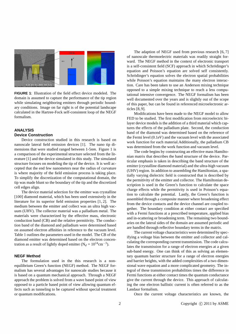
FIGURE 1: Illustration of the field effect device modeled. Thedomain is assumed to capture the performance of the tip regionwhile simulating neighboring emitters through periodic bound-ary conditions. Image on far right is of the potential landscapecalculated in the Hartree-Fock self-consistent loop of the NEGFformalism.
ANALYSISDevice Construction
Device construction studied in this research is based onnanoscale lateral field emission devices [1]. The nano tip di-mensions that were studied ranged between 1-5nm. Figure 1 isa comparison of the experimental structure selected from the lit-erature [1] and the device simulated in this study. The simulatedstructure focuses on modeling the tip of the device. It is well ac-cepted that the end few nanometers near the radius of curvatureis where majority of the field emission process is taking place.To simplify the discretization of the computational domain, thetip was made blunt so the boundary of the tip and the discretizedcell edges align.
The device material selection for the emitter was crystalline[100] diamond material, which has been used extensively in theliterature for its superior field emission properties [1, 2]. Themedium between the emitter and collect was an ultra high vac-uum (UHV). The collector material was a palladium metal. Thematerials were characterized by the effective mass, electronicconduction band (CB) and the relative permitivity. The conduc-tion band of the diamond and palladium were determined basedon assumed electron affinities in reference to the vacuum level.Table 1 outlines the parameters used in the model. The CB of thediamond emitter was determined based on the electron concen-tration as a result of lightly doped emitter (Nd = 1014cm−3).
NEGF MethodThe formulation used in the this research is a non-
equilibrium Green’s function (NEGF) method. The NEGF for-malism has several advantages for nanoscale studies because itis based on a quantum mechanical approach. Through a NEGFapproach the problem is solved from a wave based point of viewopposed to a particle based point of view allowing quantum ef-fects such as tunneling to be captured without special treatmentor quantum modifications.
The adaption of NEGF used from previous research [6, 7]of nanoscale thermoelectric materials was readily straight for-ward. The NEGF method in the context of electronic transportis a self-consistent field (SCF) approach in which Schrodinger’sequation and Poisson’s equation are solved self consistently.Schrodinger’s equation solves the electron spatial probabilitieswhile Poisson’s equation maintains the many electron interac-tion. Care has been taken to use an Anderson mixing techniqueopposed to a simple mixing technique to reach a less compu-tational intensive convergence. The NEGF formalism has beenwell documented over the years and is slightly out of the scopeof this paper, but can be found in referenced microelectronic ar-ticles [8,9].
Modifications have been made to the NEGF model to allowFED to be studied. The first modification from microelectric bi-layer device models is the addition of a third material which cap-tures the effects of the palladium plate. Second, the conductionband of the diamond was determined based on the reference ofthe Fermi level (0.1eV) and the vacuum level with the associatedwork function for each material.Additionally, the palladium CBwas determined from the work function and vacuum level.
The code begins by constructing an effective mass Hamilto-nian matrix that describes the band structure of the device. Par-ticular emphasis is taken in describing the band structure of theemitter (crystalline diamond material) and the ultra-high vacuum(UHV) region. In addition to assembling the Hamiltonian, a spa-tially varying dielectric field is constructed that is described bythe permitivity of the emitter and collector. The Hamiltonian de-scription is used in the Green’s function to calculate the spacecharge effects while the permitivity is used in Poisson’s equa-tion to calculate the potential. Lastly, the Green’s function isassembled through a composite manner where broadening effectfrom the device contacts and the device channel are coupled to-gether. The boundary condition at either contact are specifiedwith a Fermi functions at a prescribed temperature, applied biasand in-scattering or broadening term. The remaining two bound-aries on the lateral sides of the domain are assumed periodic andare handled through reflective boundary terms in the matrix.
The current voltage characteristics were determined by spec-ifying a voltage bias between the emitter and collector and cal-culating the corresponding current transmission. The code calcu-lates the transmission for a range of electron energies at a givensub-band energy. One can think of this as solving an elemen-tary quantum barrier structure for a range of electron energiesand barrier heights, with the added complexities of a two dimen-sional wave equation and a more complicated geometry. The in-tegral of these transmission probabilities times the difference inFermi functions at either contact times the quantum conductancegive the current through the device. This approach of calculat-ing the one electron ballistic current is often referred to as theLandaur formalism.
Once the current voltage characteristics are known, the
2 Copyright c© 2011 by ASME
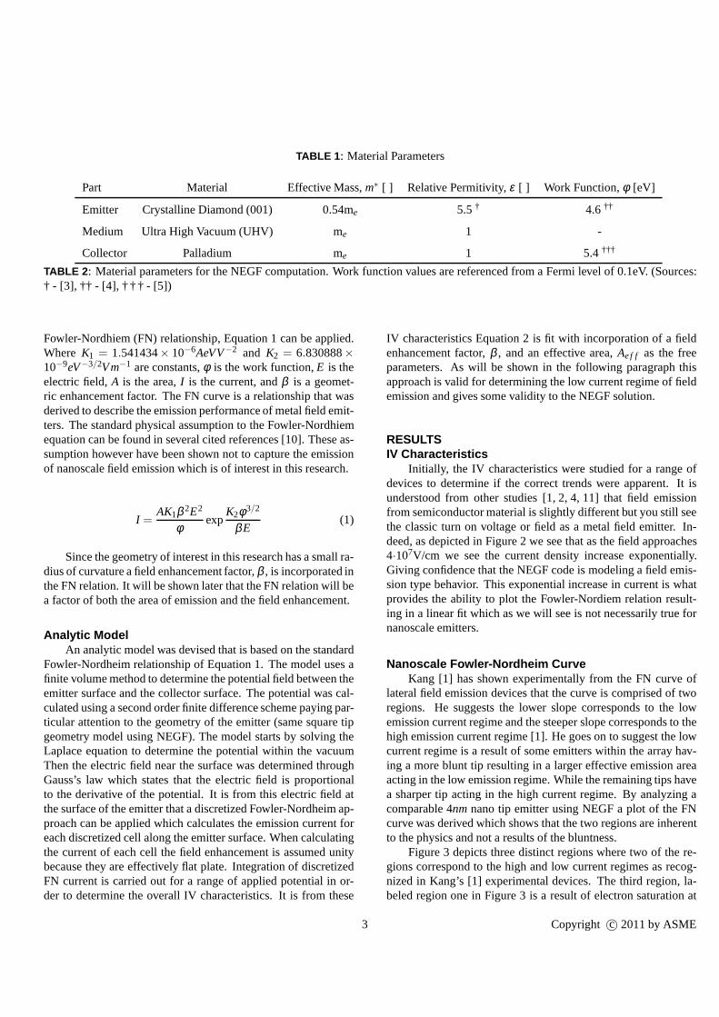
TABLE 1: Material Parameters
Part Material Effective Mass,m∗ [ ] Relative Permitivity,ε [ ] Work Function,φ [eV]
Emitter Crystalline Diamond (001) 0.54me 5.5 † 4.6††
Medium Ultra High Vacuum (UHV) me 1 -
Collector Palladium me 1 5.4†††
TABLE 2: Material parameters for the NEGF computation. Work function values are referenced from a Fermi level of 0.1eV. (Sources:† - [3], †† - [4], † † † - [5])
Fowler-Nordhiem (FN) relationship, Equation 1 can be applied.Where K1 = 1.541434× 10⁻⁶AeVV−2 and K2 = 6.830888×10⁻⁹eV−3/2Vm−1 are constants,φ is the work function,E is theelectric field,A is the area,I is the current, andβ is a geomet-ric enhancement factor. The FN curve is a relationship that wasderived to describe the emission performance of metal field emit-ters. The standard physical assumption to the Fowler-Nordhiemequation can be found in several cited references [10]. These as-sumption however have been shown not to capture the emissionof nanoscale field emission which is of interest in this research.
I =AK1β 2E2
φexp
K2φ3/2
βE(1)
Since the geometry of interest in this research has a small ra-dius of curvature a field enhancement factor,β , is incorporated inthe FN relation. It will be shown later that the FN relation will bea factor of both the area of emission and the field enhancement.
Analytic ModelAn analytic model was devised that is based on the standard
Fowler-Nordheim relationship of Equation 1. The model uses afinite volume method to determine the potential field between theemitter surface and the collector surface. The potential was cal-culated using a second order finite difference scheme paying par-ticular attention to the geometry of the emitter (same square tipgeometry model using NEGF). The model starts by solving theLaplace equation to determine the potential within the vacuumThen the electric field near the surface was determined throughGauss’s law which states that the electric field is proportionalto the derivative of the potential. It is from this electric field atthe surface of the emitter that a discretized Fowler-Nordheim ap-proach can be applied which calculates the emission current foreach discretized cell along the emitter surface. When calculatingthe current of each cell the field enhancement is assumed unitybecause they are effectively flat plate. Integration of discretizedFN current is carried out for a range of applied potential in or-der to determine the overall IV characteristics. It is from these
IV characteristics Equation 2 is fit with incorporation of a fieldenhancement factor,β , and an effective area,Ae f f as the freeparameters. As will be shown in the following paragraph thisapproach is valid for determining the low current regime of fieldemission and gives some validity to the NEGF solution.
RESULTSIV Characteristics
Initially, the IV characteristics were studied for a range ofdevices to determine if the correct trends were apparent. It isunderstood from other studies [1, 2, 4, 11] that field emissionfrom semiconductor material is slightly different but you still seethe classic turn on voltage or field as a metal field emitter. In-deed, as depicted in Figure 2 we see that as the field approaches4·107V/cm we see the current density increase exponentially.Giving confidence that the NEGF code is modeling a field emis-sion type behavior. This exponential increase in current is whatprovides the ability to plot the Fowler-Nordiem relation result-ing in a linear fit which as we will see is not necessarily true fornanoscale emitters.
Nanoscale Fowler-Nordheim CurveKang [1] has shown experimentally from the FN curve of
lateral field emission devices that the curve is comprised of tworegions. He suggests the lower slope corresponds to the lowemission current regime and the steeper slope corresponds to thehigh emission current regime [1]. He goes on to suggest the lowcurrent regime is a result of some emitters within the array hav-ing a more blunt tip resulting in a larger effective emission areaacting in the low emission regime. While the remaining tips havea sharper tip acting in the high current regime. By analyzing acomparable 4nmnano tip emitter using NEGF a plot of the FNcurve was derived which shows that the two regions are inherentto the physics and not a results of the bluntness.
Figure 3 depicts three distinct regions where two of the re-gions correspond to the high and low current regimes as recog-nized in Kang’s [1] experimental devices. The third region, la-beled region one in Figure 3 is a result of electron saturation at
3 Copyright c© 2011 by ASME

0
5e+10
1e+11
1.5e+11
2e+11
2.5e+11
3e+11
0 2e+07 4e+07 6e+07 8e+07 1e+08
J [A
/cm
2 ]
F [V/cm]
NEGF
FIGURE 2: Plot of the current voltage characteristics of a 4nmdiamond tip emitter. Modeling of an experimental diamond lat-eral nanotip emitter [1].
the tip. This saturation of the current is a result of a finite num-ber of states near the surface of the tip. As these states becomeoccupied and a large charge built up due to space charge effects,saturate of the current causes a decrease in emission current. Itseems Kang did not increases the voltage high enough to see asaturation of the current in the FN curve.
The regions labeled two and three in Figure 3 are not aswell understood at this time and require additional investigation.However, it can be certain that these high and low current re-gions of the FN curve are a function of the electron physics andnot a function of two different tip geometries as pointed out byKang [1]. It may be true that the slope of these lines are affectedby the radius of curvature of the tips.
It was determined that in order to fit the FN curve to theEquation 1 an additional parameter termed the effective area,Ae f f was required. This can be reasoned intuitively by arguingthat the true area of emission at the tip is not known. The modi-fied FN relation is as follows with an effective area parameter.
ln(I
E2 ) = ln(Ae f fAK1β 2
φ)−
K2φ3/2
βE(2)
As is seen in Figure 3 and outlined in Table 4 both the fieldenhancement factor and the effective area of emission are func-tion of the emission. Equation 2 was initially fit with just a fieldenhancement factor,β , however it didn’t capture the trends of thecurve. The trends suggest that as the applied field is increased thearea of the emission increases and the geometric influence is de-creased. Essentially, the area in which electrons are injected intothe vacuum is getting larger.
TABLE 3: Material Parameters
Model β Effective Area,Ae f f
HFE 0.814 1.874×10¹⁴
LFE 5.98 8.324×10⁻¹
Analytic 30.2 9.644×10⁻⁵
TABLE 4: Values of field enhancement factor,β , and effectivearea,Ae f f , for a 4nm emitter. A = 5.5× 10⁻⁷cm. These val-ues correspond to Figure 3. HFE corresponds to the high fieldemission and LFE corresponds to the low field emission regime.
FIGURE 3: Plot of a 4nm tip diamond emission with a bias rangefrom 0V to 9V. A high and low field emission regime exist thatis apparent in experimental data as well as NEGF simulations.
Surface StatesAs alluded to in the explanation of the current saturation in
region one of Figure 2, the surface states and states within the tipcontrol the emission properties. In the analytic treatment of fieldemission the local density of states (LDOS) or the total avail-able states is often calculated using a simple scalar addition ofstates within the tip plus the states of the surface [12]. This the-ory has been applied to absorbents and other surface treatmentsto increase the emission performance. However, when dealingwith semiconductor type material there are additional effects thatchange the band structure. One of the additional effects that willturn out to be critical in capturing is the band bending within thenano tip. The theory of band bending is well understood in themicroelectronic community and is a result of the charge distribu-tion in the device. This same theory of band bending is presentin field emission and thus the self-consistent NEGF model is agood candidate to capture the physics.
4 Copyright c© 2011 by ASME
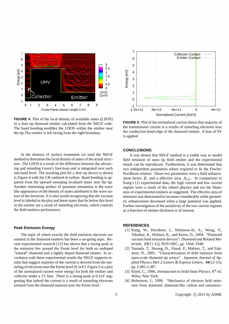
FIGURE 4: Plot of the local density of available states (LDOS)in a 4nm tip diamond emitter calculated from the NEGF code.The band bending modifies the LDOS within the emitter nearthe tip.The emitter is left facing from the right boundary.
In the absence of surface treatments we used the NEGFmethod to determine the local density of states of the actual struc-ture. The LDOS is a result of the difference between the advanc-ing and retarding Green’s functions and is integrated over eachsub-band level. The resulting plot for a 4nm tip device is shownis Figure 4 with the CB outlined in yellow. Band bending is ap-parent from the upward sweeping localized states near the tip.Another interesting artifact of quantum simulation is the wavelike appearance of the density of states attributed to the wave na-ture of the fermions. It is also worth recognizing that the vacuumlevel is labeled in the plot and these states that lie below this levelin the emitter are a result of tunneling electrons, which controlsthe field emitters performance.
Peak Emission Energy
The topic of where exactly the field emission electrons areemitted in the diamond emitters has been a on-going topic. Re-cent experimental research [13] has shown that a strong peak inthe emission lies around the Fermi level for both an undoped”natural” diamond and a lightly doped diamond emitter. In ac-cordance with these experimental results the NEGF supports re-sults that suggest majority of the current is derived from the tun-neling of electrons near the Fermi level (0.1eV). Figure 5 is a plotof the normalized current verse energy for both the emitter andcollector under a 1V bias. There is a strong peak at 0.1eV sug-gesting that indeed the current is a result of tunneling electronsemitted from the diamond material near the Fermi level.
-1
0
1
2
3
4
5
6
7
-1.2e+12 -8e+11 -4e+11 0 4e+11
Ene
rgy
[eV
]
Normalized Current [A/eV]
Collector ContactEmitter Contact
FIGURE 5: Plot of the normalized current shows that majority ofthe transmission current is a results of tunneling electrons nearthe conduction band edge of the diamond emitter. A bias of 9Vis applied
CONCLUSIONSIt was shown that NEGF method is a viable way to model
field emission of nano tip field emitter and the experimentaltrends can be reproduced. Furthermore, it was determined thattwo independent parameters where required to fit the Fowler-Nordheim relation. Those two parameters were a field enhance-ment factor,β , and a effective area,Ae f f. In comparison toKang’s [1] experimental data, the high current and low currentregime were a result of the inherit physics and not the blunt-ness of experimental emitters as suggested. The effective area ofemission was determined to increase considerably while geomet-ric enhancement decreased when a large potential was applied.Further investigation of the sensitivity of the two current regimesas a function of emitter thickness is of interest.
REFERENCES[1] Kang, W., Davidson, J., Wisitsora-At, A., Wong, Y.,
Takalkar, R., Holmes, K., and Kerns, D., 2004. “Diamondvacuum field emission devices”.Diamond and Related Ma-terials, 13(11-12), NOV-DEC, pp. 1944–1948.
[2] Yamada, T., Hwang, D., Vinod, P., Makino, T., and Fuji-mori, N., 2005. “Characterization of field emission fromnano-scale diamond tip arrays”.Japanese Journal of Ap-plied Physics Part 2-Letters & Express Letters,44(12-15),pp. L385–L387.
[3] Kittel, C., 1986.Introduction to Solid State Physics, 6th ed.Wiley, New York.
[4] Robertson, J., 1999. “Mechanics of electron field emis-sion from diamond, diamond-like carbon and nanostruc-
5 Copyright c© 2011 by ASME
tured carbon”.Journal of Vacuum Science and TechnologyB, 17(2), Mar., pp. 659–665.
[5] Lide, D. R., 2007. CRC Handbook of Chemistry andPhysics, 88th Edition (Crc Handbook of Chemistry andPhysics). CRC, June.
[6] Bulusu, A., and Walker, D. G., 2007. “Modeling of thermo-electric properties of semiconductor thin films with quan-tum and scattering effects”.Journal of Heat Transfer,129(4), Apr., pp. 492–499.
[7] Musho, T. D., and Walker, D. G., 2009. “Quantum transportproperties in nanocrystalline composites for thermoelectricdevices”. In ASME/Pacific Rim Technical Conference andExhibition on Integration and Packaging of MEMS, NEMSand Electronic Systems, IPACK2009-89332.
[8] Bulusu, A., and Walker, D. G., 2008. “One-dimensionalthin-film phonon transport with generation”.Microelec-tronics Journal,39(7), July, pp. 950–956.
[9] Datta, S., 2005.Quantum Transport: Atom to Transistor.Cambridge University Press, New York.
[10] Forbes, R. G., 1999. “Refining the application of fowler-nordheim theory”.Ultramicroscopy,79(1-4), pp. 11 – 23.
[11] Chen, J., Xu, N., Deng, S., She, J., and Chen, J., 2003.“Effects of the interface and surface nanostructures on fieldemission of amorphous diamond film”.Journal of VacuumScience & Technology B,21(1), Jan-Feb, pp. 581–586.
[12] Modinos, A., 1984.Field, thermionic, and secondary elec-tron emission spectroscopy. Plenum Press.
[13] Yamaguchi, H., Kudo, Y., Masuzawa, T., Kudo, M., Ya-mada, T., Takakuwa, Y., and Okano, K., 2008. “Combinedx-ray photoelectron spectroscopy/ultraviolet photoelectronspectroscopy/field emission spectroscopy for characteriza-tion of electron-emission mechanism of diamond”.Journalof Vacuum Science & Technology B,11(3-4), pp. 127–139.
6 Copyright c© 2011 by ASME