Quantum Hall effect and Landau levels in the three ...
12
PHYSICAL REVIEW RESEARCH 2, 033003 (2020) Quantum Hall effect and Landau levels in the three-dimensional topological insulator HgTe J. Ziegler, 1 D. A. Kozlov, 2, 3 N. N. Mikhailov, 3 S. Dvoretsky , 3 and D. Weiss 1 1 Experimental and Applied Physics, University of Regensburg, D-93040 Regensburg, Germany 2 A. V. Rzhanov Institute of Semiconductor Physics, Novosibirsk 630090, Russia 3 Novosibirsk State University, Novosibirsk 630090, Russia (Received 4 February 2020; accepted 11 June 2020; published 1 July 2020) We review low- and high-field magnetotransport in 80-nm-thick strained HgTe, a material that belongs to the class of strong three-dimensional topological insulators. Utilizing a top gate, the Fermi level can be tuned from the valence band via the Dirac surface states into the conduction band and allows studying Landau quantization in situations where different species of charge carriers contribute to magnetotransport. Landau fan charts, mapping the conductivity σ xx ( V g , B) in the whole magnetic field–gate voltage range, can be divided into six areas, depending on the state of the participating carrier species. Key findings are (i) the interplay of bulk holes (spin degenerate) and Dirac surface electrons (nondegenerate), coexisting for E F in the valence band, leads to a periodic switching between odd and even filling factors and thus odd and even quantized Hall voltage values. (ii) We found a similar though less pronounced behavior for coexisting Dirac surface and conduction band electrons. (iii) In the bulk gap, quantized Dirac electrons on the top surface coexist at lower B with nonquantized ones on the bottom side, giving rise to quantum Hall plateau values depending—for a given filling factor—on the magnetic field strength. In stronger B fields, Landau level separation increases; charge transfer between different carrier species becomes energetically favorable and leads to the formation of a global (i.e., involving top and bottom surfaces) quantum Hall state. Simulations using the simplest possible theoretical approach are in line with the basic experimental findings, describing correctly the central features of the transitions from classical to quantum transport in the respective areas of our multicomponent charge carrier system. DOI: 10.1103/PhysRevResearch.2.033003 I. INTRODUCTION The quantum Hall effect (QHE) [1] and Shubnikov–de Haas (SdH) oscillations with zero resistance states [2] are hall- marks of two-dimensional electron (2DES) or hole (2DHS) systems, realized, e.g., in semiconductor heterostructures [3] or in graphene [4]. These phenomena are closely connected to the discrete Landau level (LL) spectrum of charge carriers in quantizing magnetic fields. These Landau levels are spaced by the cyclotron energy ¯ hω c (¯ h is the reduced Planck constant and ω c the cyclotron frequency) and form, as a function of magnetic field and Landau level index n, the Landau fan chart. In conventional two-dimensional systems one type of charge carrier, i.e., electrons or holes, prevails, giving rise to one Lan- dau fan chart and a regular sequence of SdH peaks or quantum Hall plateaus, which occur in equidistant steps on an inverse magnetic field scale, 1/B. A more complicated situation arises when two-dimensional electron and hole systems coexist as in heterojunctions with a broken gap (type III heterojunction), e.g., in InAs/GaSb quantum wells [5]. This gives rise to hy- bridization [6] and a complicated interplay between LLs [7]. With the advent of three-dimensional (3D) topological insula- Published by the American Physical Society under the terms of the Creative Commons Attribution 4.0 International license. Further distribution of this work must maintain attribution to the author(s) and the published article’s title, journal citation, and DOI. tors (TIs) [8–11] a new class of two-dimensional electron sys- tems appeared on the scene where the two-dimensional charge carrier system consisting of Dirac fermions forms a closed surface “wrapped” around the insulating bulk. In contrast to a conventional two-dimensional electron gas, these Dirac surface states are non–spin degenerate and have their spin orientation locked to their momentum. The unusual topology of the two-dimensional Dirac system creates a manifold of possibilities of how the charge carriers on the top and bottom surfaces interact for different positions of Fermi level and magnetic field strength. For a Fermi-level position in the conduction band, e.g., three different charge carrier species with different densities and mobilities exist: bulk electrons, which are spin degenerate, and nondegenerate Dirac surface electrons on the top and bottom surfaces. Here, we ignore charge carriers on the side facets, parallel to the applied mag- netic field, which play only a minor role in the context of the present investigations. While SdH oscillations and the QHE have been observed in various TI materials [12–17], strained HgTe, a strong topological insulator [18], is insofar special, as it features unprecedented high mobilities μ with μB 1 at magnetic fields as low as 0.1 T. This material thus serves as a model system to explore Landau quantization and mag- netotransport in a situation where different types of charge carriers exist together. However, the physics discussed below is also valid for other topological insulator materials in which different kinds of charge carriers coexist at the Fermi level. The first observation of the QHE in strained films of HgTe was reported in Ref. [12], which also presents calculations of 2643-1564/2020/2(3)/033003(12) 033003-1 Published by the American Physical Society
Transcript of Quantum Hall effect and Landau levels in the three ...

PHYSICAL REVIEW RESEARCH 2, 033003 (2020)
Quantum Hall effect and Landau levels in the three-dimensional topological insulator HgTe
J. Ziegler,1 D. A. Kozlov,2,3 N. N. Mikhailov,3 S. Dvoretsky ,3 and D. Weiss 1
1Experimental and Applied Physics, University of Regensburg, D-93040 Regensburg, Germany2A. V. Rzhanov Institute of Semiconductor Physics, Novosibirsk 630090, Russia
3Novosibirsk State University, Novosibirsk 630090, Russia
(Received 4 February 2020; accepted 11 June 2020; published 1 July 2020)
We review low- and high-field magnetotransport in 80-nm-thick strained HgTe, a material that belongs to theclass of strong three-dimensional topological insulators. Utilizing a top gate, the Fermi level can be tuned fromthe valence band via the Dirac surface states into the conduction band and allows studying Landau quantizationin situations where different species of charge carriers contribute to magnetotransport. Landau fan charts,mapping the conductivity σxx (Vg, B) in the whole magnetic field–gate voltage range, can be divided into sixareas, depending on the state of the participating carrier species. Key findings are (i) the interplay of bulk holes(spin degenerate) and Dirac surface electrons (nondegenerate), coexisting for EF in the valence band, leads toa periodic switching between odd and even filling factors and thus odd and even quantized Hall voltage values.(ii) We found a similar though less pronounced behavior for coexisting Dirac surface and conduction bandelectrons. (iii) In the bulk gap, quantized Dirac electrons on the top surface coexist at lower B with nonquantizedones on the bottom side, giving rise to quantum Hall plateau values depending—for a given filling factor—on themagnetic field strength. In stronger B fields, Landau level separation increases; charge transfer between differentcarrier species becomes energetically favorable and leads to the formation of a global (i.e., involving top andbottom surfaces) quantum Hall state. Simulations using the simplest possible theoretical approach are in linewith the basic experimental findings, describing correctly the central features of the transitions from classical toquantum transport in the respective areas of our multicomponent charge carrier system.
DOI: 10.1103/PhysRevResearch.2.033003
I. INTRODUCTION
The quantum Hall effect (QHE) [1] and Shubnikov–deHaas (SdH) oscillations with zero resistance states [2] are hall-marks of two-dimensional electron (2DES) or hole (2DHS)systems, realized, e.g., in semiconductor heterostructures [3]or in graphene [4]. These phenomena are closely connectedto the discrete Landau level (LL) spectrum of charge carriersin quantizing magnetic fields. These Landau levels are spacedby the cyclotron energy h̄ωc (h̄ is the reduced Planck constantand ωc the cyclotron frequency) and form, as a function ofmagnetic field and Landau level index n, the Landau fan chart.In conventional two-dimensional systems one type of chargecarrier, i.e., electrons or holes, prevails, giving rise to one Lan-dau fan chart and a regular sequence of SdH peaks or quantumHall plateaus, which occur in equidistant steps on an inversemagnetic field scale, 1/B. A more complicated situation ariseswhen two-dimensional electron and hole systems coexist asin heterojunctions with a broken gap (type III heterojunction),e.g., in InAs/GaSb quantum wells [5]. This gives rise to hy-bridization [6] and a complicated interplay between LLs [7].With the advent of three-dimensional (3D) topological insula-
Published by the American Physical Society under the terms of theCreative Commons Attribution 4.0 International license. Furtherdistribution of this work must maintain attribution to the author(s)and the published article’s title, journal citation, and DOI.
tors (TIs) [8–11] a new class of two-dimensional electron sys-tems appeared on the scene where the two-dimensional chargecarrier system consisting of Dirac fermions forms a closedsurface “wrapped” around the insulating bulk. In contrastto a conventional two-dimensional electron gas, these Diracsurface states are non–spin degenerate and have their spinorientation locked to their momentum. The unusual topologyof the two-dimensional Dirac system creates a manifold ofpossibilities of how the charge carriers on the top and bottomsurfaces interact for different positions of Fermi level andmagnetic field strength. For a Fermi-level position in theconduction band, e.g., three different charge carrier specieswith different densities and mobilities exist: bulk electrons,which are spin degenerate, and nondegenerate Dirac surfaceelectrons on the top and bottom surfaces. Here, we ignorecharge carriers on the side facets, parallel to the applied mag-netic field, which play only a minor role in the context of thepresent investigations. While SdH oscillations and the QHEhave been observed in various TI materials [12–17], strainedHgTe, a strong topological insulator [18], is insofar special,as it features unprecedented high mobilities μ with μB � 1at magnetic fields as low as 0.1 T. This material thus servesas a model system to explore Landau quantization and mag-netotransport in a situation where different types of chargecarriers exist together. However, the physics discussed belowis also valid for other topological insulator materials in whichdifferent kinds of charge carriers coexist at the Fermi level.
The first observation of the QHE in strained films of HgTewas reported in Ref. [12], which also presents calculations of
2643-1564/2020/2(3)/033003(12) 033003-1 Published by the American Physical Society

J. ZIEGLER et al. PHYSICAL REVIEW RESEARCH 2, 033003 (2020)
the band dispersion of the surface states on the top and bottomsurfaces. Corresponding ab initio calculations computing theband gap in which the TI surface states reside as a functionof strain (i.e., lattice mismatch between HgTe and substrate)were presented in Ref. [19]. Typical band gaps for HgTe onCdTe are of the order of 20 meV. Since in the initial exper-iment the position of the Fermi level EF was unknown, weexplored the QHE effect and SdH oscillations systematicallyas a function of a top gate voltage [13]. The top gate enablestuning the Fermi level from the valence band, through thegap region with gapless surface states into the conductionband. As the QHE is also observed when the Fermi levelis supposedly in the conduction band, Brüne et al. claimedthat due to screening effects the Fermi level is pinned inthe band gap so that only Dirac surface states exist at EF
[20]. However, the underlying “phenomenological effectivepotential for the sake of keeping the Fermi level within thebulk gap is not proper” [21]. Below we show not only thatthe Fermi level can be easily tuned from the valence bandinto the conduction band, but we provide a comprehensivepicture of Landau quantization and quantum Hall effect in themulticarrier system of a topological insulator.
II. CHARACTERIZATION OF SAMPLES
The 80-nm-thick HgTe material, investigated here, hasbeen grown by molecular beam epitaxy on (013)-oriented(GaAs); similar wafers have been used previously to studymagnetotransport [13], cyclotron resonance [22], or quantumcapacitance [23]. A π -phase shift of quantum capacitanceoscillations [23], geometric resonances in antidot arrays [24],and the subband spectrum of HgTe nanowires made of thismaterial [25] confirm the topological nature of the surfacestates. As shown in Fig. 1(a), the heterostructure includesa 20-nm-thick CdxHg1–xTe buffer layer on either side anda 40-nm-thick CdTe cap layer to protect the pristine HgTesurfaces. A top gate stack consisting of 30 nm of SiO2, 100nm of Al2O3 and Ti/Au enables control of the charge carrierdensity and thus of the Fermi level via gating. Thus, theFermi energy EF can be tuned from the valence band (VB)into the bulk gap and further into the conduction band (CB)[13,21,23]. For magnetotransport measurement we use a stan-dard Hall bar geometry of length 1100 μm and width 200 μm,sketched in Fig. 1(b), and temperatures of T = 50 mK; themagnetic field B points perpendicular to the sample plane.We use a low ac current of 10 nA flowing through the Hallbar to prevent heating of the carriers. To measure longitudinaland transversal resistivities ρxx and ρxy, respectively, we usestandard low-frequency lock-in techniques.
Figure 1(c) shows low-field SdH oscillations taken atdifferent gate voltages, i.e., Fermi level positions. At Vg =–1.5 V the Fermi level is in the valence band while for +1 Vit is in the bulk gap; a simplified band structure is shownin Fig. 2(a) for guidance. Figure 1(d) displays the typical Vg
dependence of the resistivity ρxx, measured at B = 0, and ofthe Hall resistance ρxy, taken at 0.5 T. The traces are verysimilar to the ones we reported previously [13,23–26]. Theρxx trace exhibits a maximum at Vg = −0.15 V near the chargeneutrality point (CNP, at Vg = 0.25 V), and two characteristicweak humps at 0.4 and 1.25 V. The latter are due to enhanced
FIG. 1. (a) Scheme of the heterostructure cross section. (b)Sketch of the 200-µm-wide and 1100-µm-long Hall bar. (c) Lon-gitudinal resistivity ρxx (B) at different Vg for EF in the conductionband (2, 1.5 V), gap (1 V), and valence band (–0.5, −1.5 V).(d) Vg dependence of ρxx (left axis, light blue) at B = 0 and ρxy (rightaxis, dark blue) at B = 0.5 T. The vertical arrows show the chargeneutrality point (CNP), top of the bulk valence (EV ), and bottom ofthe conductance band (EC), respectively. Here, EV and EC mark thegate voltage at which bulk hole and bulk electron densities vanish,respectively. (e) Electron ns(Vg) and hole densities ps(Vg) extractedfrom the Hall slope, two-carrier Drude model, and SdH oscillations.The analysis follows Ref. [13] and yields positions of the valenceand conduction band edges at Vg(EV ) = 0.45 V and Vg(EC ) = 1.2 V,respectively, marked in (d). (f) Pictorial of the capacitively coupledlayers in the 3D TI sample which form the basis of our electrostaticmodel. (g) Electron ns(Vg) and hole densities ps(Vg) as calculatedwith our electrostatic model. The densities which can be directlycompared with (e) are shown as solid lines, the ones which are notdirectly accessible as dashed lines.
scattering of surface electrons and bulk carriers at the bandedges, i.e., valence band (VB, marked by EV on the Vg axis)and conduction band (CB, marked EC) [13]. Near the CNPthe Hall resistance ρxy changes sign as the majority chargecarrier type changes from electrons to holes when EF entersthe VB. Closer examination of magnetotransport data usingthe Drude model and the periodicity of SdH oscillations, asin Refs. [13,23], reveals partial densities and precise values ofEV and EC . The result of such analysis is shown in Fig. 1(e).Above EV , electron densities ns are extracted from the slopeof the Hall resistance (nHall
s ) and from the periodicity ofthe SdH oscillations. SdH oscillation periods reveal differentcarrier densities, depending on whether the data are taken atlow (nSdH,low
s ) or high magnetic fields (nSdH,highs ). While nHall
s
and nSdH,highs represent the total charge carrier density of the
system (and therefore coincide), nSdH,lows represents the top
surface electrons only [13,23]. The reason for the latter is
033003-2
QUANTUM HALL EFFECT AND LANDAU LEVELS IN THE … PHYSICAL REVIEW RESEARCH 2, 033003 (2020)
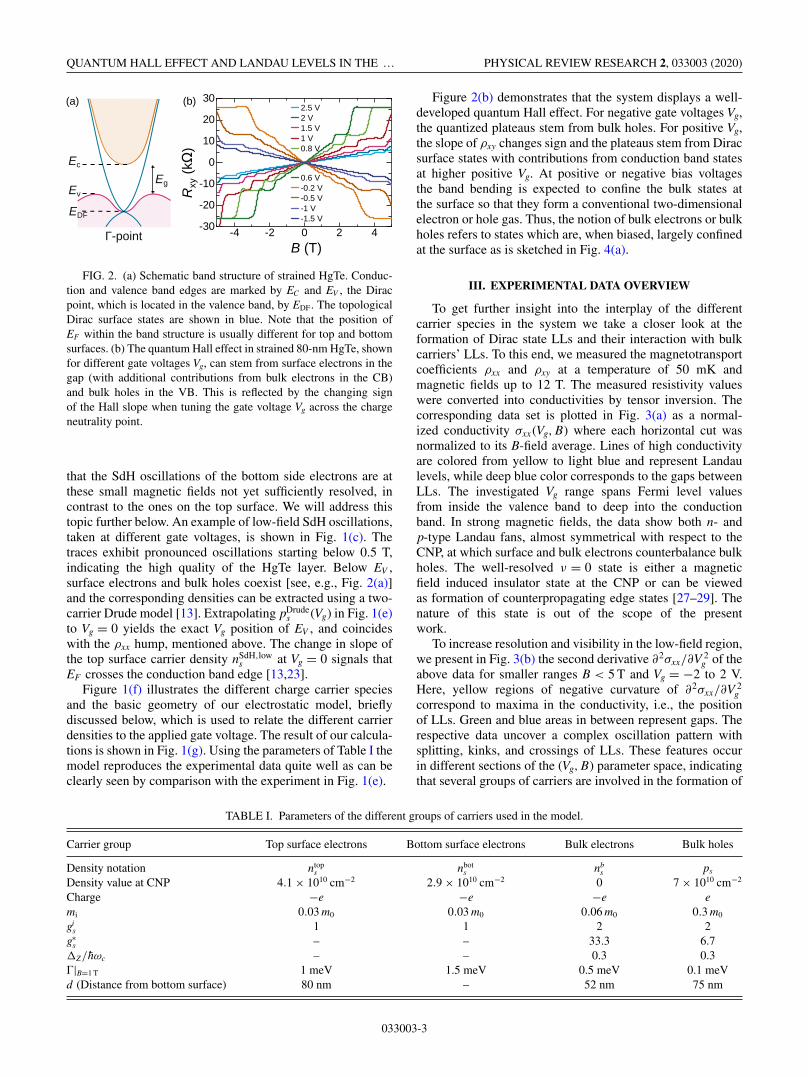
FIG. 2. (a) Schematic band structure of strained HgTe. Conduc-tion and valence band edges are marked by EC and EV , the Diracpoint, which is located in the valence band, by EDF. The topologicalDirac surface states are shown in blue. Note that the position ofEF within the band structure is usually different for top and bottomsurfaces. (b) The quantum Hall effect in strained 80-nm HgTe, shownfor different gate voltages Vg, can stem from surface electrons in thegap (with additional contributions from bulk electrons in the CB)and bulk holes in the VB. This is reflected by the changing signof the Hall slope when tuning the gate voltage Vg across the chargeneutrality point.
that the SdH oscillations of the bottom side electrons are atthese small magnetic fields not yet sufficiently resolved, incontrast to the ones on the top surface. We will address thistopic further below. An example of low-field SdH oscillations,taken at different gate voltages, is shown in Fig. 1(c). Thetraces exhibit pronounced oscillations starting below 0.5 T,indicating the high quality of the HgTe layer. Below EV ,surface electrons and bulk holes coexist [see, e.g., Fig. 2(a)]and the corresponding densities can be extracted using a two-carrier Drude model [13]. Extrapolating pDrude
s (Vg) in Fig. 1(e)to Vg = 0 yields the exact Vg position of EV , and coincideswith the ρxx hump, mentioned above. The change in slope ofthe top surface carrier density nSdH,low
s at Vg = 0 signals thatEF crosses the conduction band edge [13,23].
Figure 1(f) illustrates the different charge carrier speciesand the basic geometry of our electrostatic model, brieflydiscussed below, which is used to relate the different carrierdensities to the applied gate voltage. The result of our calcula-tions is shown in Fig. 1(g). Using the parameters of Table I themodel reproduces the experimental data quite well as can beclearly seen by comparison with the experiment in Fig. 1(e).
Figure 2(b) demonstrates that the system displays a well-developed quantum Hall effect. For negative gate voltages Vg,the quantized plateaus stem from bulk holes. For positive Vg,the slope of ρxy changes sign and the plateaus stem from Diracsurface states with contributions from conduction band statesat higher positive Vg. At positive or negative bias voltagesthe band bending is expected to confine the bulk states atthe surface so that they form a conventional two-dimensionalelectron or hole gas. Thus, the notion of bulk electrons or bulkholes refers to states which are, when biased, largely confinedat the surface as is sketched in Fig. 4(a).
III. EXPERIMENTAL DATA OVERVIEW
To get further insight into the interplay of the differentcarrier species in the system we take a closer look at theformation of Dirac state LLs and their interaction with bulkcarriers’ LLs. To this end, we measured the magnetotransportcoefficients ρxx and ρxy at a temperature of 50 mK andmagnetic fields up to 12 T. The measured resistivity valueswere converted into conductivities by tensor inversion. Thecorresponding data set is plotted in Fig. 3(a) as a normal-ized conductivity σxx(Vg, B) where each horizontal cut wasnormalized to its B-field average. Lines of high conductivityare colored from yellow to light blue and represent Landaulevels, while deep blue color corresponds to the gaps betweenLLs. The investigated Vg range spans Fermi level valuesfrom inside the valence band to deep into the conductionband. In strong magnetic fields, the data show both n- andp-type Landau fans, almost symmetrical with respect to theCNP, at which surface and bulk electrons counterbalance bulkholes. The well-resolved ν = 0 state is either a magneticfield induced insulator state at the CNP or can be viewedas formation of counterpropagating edge states [27–29]. Thenature of this state is out of the scope of the presentwork.
To increase resolution and visibility in the low-field region,we present in Fig. 3(b) the second derivative ∂2σxx/∂V 2
g of theabove data for smaller ranges B < 5 T and Vg = −2 to 2 V.Here, yellow regions of negative curvature of ∂2σxx/∂V 2
gcorrespond to maxima in the conductivity, i.e., the positionof LLs. Green and blue areas in between represent gaps. Therespective data uncover a complex oscillation pattern withsplitting, kinks, and crossings of LLs. These features occurin different sections of the (Vg, B) parameter space, indicatingthat several groups of carriers are involved in the formation of
TABLE I. Parameters of the different groups of carriers used in the model.
Carrier group Top surface electrons Bottom surface electrons Bulk electrons Bulk holes
Density notation ntops nbot
s nbs ps
Density value at CNP 4.1 × 1010 cm−2 2.9 × 1010 cm−2 0 7 × 1010 cm−2
Charge −e −e −e emi 0.03 m0 0.03 m0 0.06 m0 0.3 m0
gis 1 1 2 2
g∗s – – 33.3 6.7
�Z/h̄ωc – – 0.3 0.3Г|B=1 T 1 meV 1.5 meV 0.5 meV 0.1 meVd (Distance from bottom surface) 80 nm – 52 nm 75 nm
033003-3

J. ZIEGLER et al. PHYSICAL REVIEW RESEARCH 2, 033003 (2020)
FIG. 3. (a) Color map of the normalized longitudinal conductivity σxx (Vg, B) for magnetic fields up to B = 12 T. Conductance maxima areyellow and green; filling factors for the bluish energy gaps are shown in white. Data are normalized to the average value for a given B value.We use a logarithmic color scale to enhance the visibility of features throughout the entire investigated parameter space. (b) Excerpt of the datain (a), shown as the second derivative ∂2σxx/∂V 2
g . Yellow lines correspond, as above, to Landau levels, and green and blue regions to Landaugaps. White dashed lines separate the investigated parameter space (Vg, B) into distinct sections discussed in the text. (c) Simulated densityof states based on the simple model described in the Appendix. Maxima (minima) of the DoS are shown in yellow (blue) and correspond tomaxima (minima) of σxx (Vg, B), i.e., to LL positions (gaps). EV , EC , CNP, and EDF,top label points on the gate voltage axis, which were matchedto the experimentally obtained values. White lines represent the fan chart originating from the CNP.
LLs. The analysis of the data can be done in several ways.One option is to exactly calculate LL positions using thek · p method and trying to fit the whole set of data. However,such an approach entails significant computational difficultiesbecause Schrödinger and Poisson equations need to be calcu-lated self-consistently for every point in the (Vg, B) parameterspace. Still, this procedure would not promote true insightinto the underlying physics. Instead, we introduce a minimalbut adequate computational model, which semiquantitativelyagrees with the experimental data. The model is based on ourcapacitance model [23] but extended to the case of nonzeromagnetic fields. While its detailed description is presentedin the Appendix, we address here only the crucial points:Within the model, each group of carriers is characterized byits own set of LLs, typified by the charge they carry (emptyLLs bear no charge, while occupied ones are negatively orpositively charged), Landau degeneracy (spin degenerate ornot), LL dispersion, and LL broadening. Further, a joint Fermilevel EF and the total charge carrier density (ns − ps), whichdepends linearly on Vg, characterize the entire system. Thetotal charge is distributed among all LLs, determined by theposition of the Fermi level. Here, we need to take into accountthe electrostatics of the system: Changes of the electric fieldsin the device due to changes of the carrier densities withinthe subsystem via the gate shifts the band edges and thus thecorresponding origins of the LLs. The effect of electrostaticson the position of LLs for several gate voltages is shown inFig. 4, described in more detail in the caption and in Fig. S1
in the Supplemental Material [30]. It is important to notethat the band edges and thus the origin of the LL fan chartsdepend on the gate voltage Vg. In the limit of zero magneticfield, the model gives identical results (i.e., bands bending andpartial densities) as the capacitance model [23]. The outputof the calculation is the position of the Fermi level, bothpartial νi and total filling factors ν, partial densities of states(DOS) Di, and Hall conductivities σ i
xy for specified B and Vg
values. Figure 3(c) shows an example of such a calculationwhich displays the total density of states as a function of Vg
and B, thus reconstructing the LLs within the (Vg, B) map.Above 4 T on the hole side and above 6–8 T on the electronside the calculated LLs form simple fan charts which bothemanate from the CNP. This is in excellent agreement withthe experiment in Fig. 3(a).
The combined analysis of experimental data and simu-lations allows us to classify six distinct regions within theσxx(Vg, B) map, shown in Fig. 3(b). We will discuss theregions marked from 1 to 6 below with the help of ourmodel calculations. Region 1 covers the high-magnetic-fieldregion where the system is fully quantized, so that all LLs areresolved. Here, the total density ns − ps determines the fillingfactors and the Landau level positions. By extrapolating theLLs in Fig. 3(a) from high fields down to B = 0 (not shown)all the lines meet at the CNP. Conversely, region 6 locatedat fields below 0.4 T describes fully classical and diffusivetransport. At intermediate magnetic fields, i.e., in large partsof regions 2–5, only some of the LLs, e.g., on the top surface,
033003-4

QUANTUM HALL EFFECT AND LANDAU LEVELS IN THE … PHYSICAL REVIEW RESEARCH 2, 033003 (2020)
EF
Ec
Ev
DFbott
Ec
Ev
Ec
Ev
Ec
Ev
DFtop DFbott DFtop DFbott DFtop DFbott
EF
(a)
0 1 2 3 4-20
-15
-10
-5
0
5
10
15
20
0 1 2 3 4 0 1 2 3 4-20
-15
-10
-5
0
5
10
15
20
0 1 2 3 4
Ev
Ec
EDF, top
EDF, bot
Vg = -1.5 V(Valence band)
(b)
Vg = 0.25 V(CNP)
B (T)
)Ve
m( E
Vg = 1.5 V(Cond band)
Vg = 0.9 V(Gap)
DFtop
FIG. 4. When a gate voltage is applied, the charge carriers of the system rearrange. While the exact solution requires a complicatedself-consistent solution of Schrödinger and Poisson equations, most of the features observed in magnetotransport can be explained by a simpleelectrostatic model. Within this model, each group of carriers is modeled by a 2D system of electrons or holes of zero thickness. Each layergenerates its own set of Landau levels emerging at different energies, but with common Fermi level position. Charged 2D surfaces cause, likea charged capacitor plate, 1D electric fields across the structure leading to electrostatic potentials, depending linearly on the charge. Thesepotentials change with gate voltage, thus shifting the band edges, from which the Landau levels emanate. (a) Schematic band diagrams ofthe investigated HgTe 3D TI system at different gate voltages Vg (VB: Vg = –1.5 V; CNP: Vg = 0.25 V; gap: Vg = 0.9 V; CB: Vg = 1.5 V).Occupied hole states are shown in red, occupied states of surface electrons in dark blue, and bulk states in orange. The Dirac points of topand bottom surfaces in strained HgTe thin films are located below EV , as shown in the diagrams. (b) Landau level spectra at different biasconditions used in the model. The corresponding band bending is shown above in (a). The model calculations include Zeeman splitting forspin-degenerate bulk states (orange for conduction band; red for valence band states). Landau fans that do not cross the Fermi energy EF (i.e.,empty levels) are shown as dotted lines.
are resolved so that combinations of quantized and diffusivetransport arise. In region 4, EF is in the gap so that onlytopological states on the top and bottom surfaces are presentat the Fermi level, but no bulk states. In regions 2 and 3, bulkholes dominate the Landau spectrum but coexist with surfaceelectrons on top and bottom. The coexisting surface electronand bulk hole Landau fans cause an intricate checkerboardpattern in region 3. In region 5, the surface states coexistwith bulk electrons that are filled when EF > EC . Below, weconsider these regions in more detail.
IV. WEAK AND STRONG MAGNETIC FIELD LIMITS
The behavior of the system in the limits of small andlarge magnetic fields is easily accessible. At small magneticfields, i.e., in region 6 of Fig. 3(b), the LL separation issmaller than the LL broadening and transport is fully dif-fusive. In this regime the classical multicomponent Drude
model characterizes transport. The model assigns each groupof carriers, labeled by index i, its own set of density ns,i andmobility μi. The resulting total conductivity is then the sumof the partial conductivities [13,31]. This model explains theobserved effects, including the nonlinear ρxy(B) trace as wellas a distinct positive magnetoresistance when bulk holes andsurface electrons coexist in the valence band [13]. The verylow density of bulk carriers in the gap is reflected by thedarker blue color (i.e., low σxx) with a sharp transition at theconduction band edge Vg(EC ) and a smoother one at Vg(EV )in Fig. 3(a). The color difference between gap and bulk bandsregions reflects the effect of classical localization of chargecarriers described by σxx,i ∝ ns,i/μiB2 in classically strongfields (μB � 1, here typically valid for B > 0.1 T). Thus, themagnetoconductivity σxx is lowest in the gap where the bulkcarrier concentration with low mobility is significantly lowerthan the one in conduction band. The contrast of the color atEC in Fig. 3(a) directly confirms that the Fermi level can be
033003-5

J. ZIEGLER et al. PHYSICAL REVIEW RESEARCH 2, 033003 (2020)
tuned into the conduction band, in contrast to earlier claims[20].
The opposite case of strong magnetic fields is characterizedby completely (spin) resolved LLs and well-defined QHEstate. On the electron side, e.g., three fan charts—one for thetop surface, one for the bottom surface, and, for the Fermilevel in the conduction band, one for bulk electrons—coexist.For constant carrier density (gate voltage), the Fermi leveljumps with increasing magnetic field from a fully occupied LLof the top surface electrons to the next lower one, belonging,e.g., to the electrons on the bottom surface. This processis connected with a transfer of charges from the top to thebottom surface. The SdH oscillations reflect, in this case,the total carrier density of bottom plus top surface electrons.The total charge density ns − ps controls the total filling factorν and the position of the Landau levels. On the electron side,this means that the total electron density (bulk plus surfacedensity) determines the filling factor, while in the valenceband (where surface electrons and bulk holes coexist) it isthe difference of electron and hole densities. The Landau fanchart, constructed from high-field σxx data in Fig. 3(a), issymmetric with respect to the CNP and periodic in Vg and1/B. The entire high-field LLs in Fig. 3(a), extrapolated tozero magnetic field, have their origin at the CNP. The patternis very similar to that observed in other electron-hole systems,e.g., in graphene [4,32], but without graphene’s spin andvalley degeneracy. However, there is a quantitative asymmetrybetween electrons (positive filling factors) and holes (negativefilling factors): The conductivity minima for electrons aredeeper than for holes; at the same time, the conductivitymaxima are broader for holes. This asymmetry reflects thedifference of effective masses and cyclotron gaps, which differby one order of magnitude [22,33] between the carrier types.The transition between the low-field regime, at which the LLfans are determined by the respective electron or hole density,and the high-field regime, where the fans follow the totalcharge carrier density ns − ps, occurs when the LL separationis sufficiently large compared to the LL broadening.
V. COEXISTENCE OF QUANTIZED AND DIFFUSIVECARRIERS IN THE BULK GAP
Here we focus on the bulk gap region, labeled as region 4 inFig. 3(b) and magnified in Fig. 5(a). In this region, the Fermilevel is in the bulk gap and only Dirac surface states contributeto transport. The SdH oscillations appear from 0.3 T onand show a uniform pattern, strictly periodic in Vg and 1/B,until a magnetic field of B = 1.5–2 T is reached. This regularbehavior reflects that only the motion of one carrier species,i.e., the electrons on the top surface, is quantized [13,23].The electrons on the bottom surface have lower density andmobility and their LL spectrum is not yet resolved. Thebottom electrons thus contribute a featureless background tothe conductivity. The σxy(Vg) data in Fig. 5(c) clearly show thisdiffusive background: The individual low-field σxy(Vg) tracesshow pronounced nonquantized Hall plateaus with values,which increase with increasing B field [see red dashed linesin Fig. 5(c)]. This behavior can be reproduced by adding theHall conductivities of the top and bottom surface electrons:σ tot
xy = σquantxy + σ diff
xy = ν top e2/h + μ nbots e μB/(1 + (μB)2).
Here, σquantxy is the quantized Hall conductivity of the top
surface, depending on the corresponding filling factor ν top andthe carrier density of the back surface, nbot
s , which dependsonly weakly on the gate voltage. We estimate the increaseof the plateau values with increasing B in the SupplementalMaterial [30], which is in good agreement with experiment.
The SdH oscillations occurring below 1.5 T are describedby a single fan chart, shown as dark blue lines in Fig. 5(a).The fan chart emerges at Vg = 0.05 V, corresponding to aposition of the Fermi level in the valence band. This pointcan be viewed as a virtual Dirac point, at which the densityof the top surface Dirac seemingly becomes zero. However,this would only be the case if the filling rate of the top surfaceelectrons was constant, which is not the case. When EF entersthe valence band, the filling rate decreases precipitously andthe fan chart no longer fits the observed σxy maxima [see darkblue dashed lines in Fig. 5(a)]. The actual gate voltage atwhich ntop
s = 0 holds is located much deeper in the valenceband and labeled EDF, top, shown in Fig. 5(b). Typical partialdensities of the different charge carriers and the correspondingfilling rates, extracted from our experiments, are sketched inFigs. S1(a) and S1(b) [30].
Below a magnetic field strength of about 1.5 T, the surfaceelectrons on the bottom side do not contribute to the oscilla-tory part of σxx. This is an important distinction to other well-studied two-component systems such as wide GaAs quantumwells [34–36], where SdH oscillations of different frequenciesappear on a 1/B scale. At larger fields (B > 2 T), bottomsurface electrons contribute to quantum transport. This resultsin extra structure in the SdH oscillations, which breaks theregularity of the fan chart of Fig. 5(a). In this regime theσxy plateaus, shown in Fig. 5(c), become quantized in unitsof e2/h. The data suggest that the transition from classical toquantum transport appears at different magnetic fields for topand bottom surfaces (0.3 and 1.5 T, respectively). This mightbe caused by significantly different degrees of LL broadeningfor electrons on top and bottom surfaces; however, this isnot obligatory. The simulation shown in Fig. 6(a) shows thatthe SdH oscillations stemming from the top surface dominateeven if one assumes the same disorder and mobility for topand bottom surface electrons. Figure 6(a) shows the totaldensity of states of top surface and bottom surface states. Thedark blue fan chart, however, is that of the top surface onlybut matches the total DOS perfectly. The fan chart of the backsurface has an observably different origin and periodicity (seeFig. S2(b) in the Supplemental Material [30]). The top surfacedominates the overall density of states because of its 2.5times higher carrier density and thus higher SdH oscillationfrequency.
VI. VALENCE BAND: SPIN-DEGENERATE HOLESAND SPIN-RESOLVED ELECTRONS
The most striking feature in transport and thus in the LLfan chart arises from coexisting surface electrons and bulkholes in regions 2 and 3 [see Fig. 3(b) and magnification inFigs. 5(b) and 5(e)], each characterized by its own set of LLs.Note that in the valence band both top and bottom surfaceelectrons are present. However, only the top surface electronsparticipate in the formation of the observed oscillations. The
033003-6

QUANTUM HALL EFFECT AND LANDAU LEVELS IN THE … PHYSICAL REVIEW RESEARCH 2, 033003 (2020)
FIG. 5. (a) ∂2σxx/∂V 2g for B up to 3 T and Vg > 0 covering the bulk gap and conduction band region. Dark blue lines retrace the Landau
levels. The Landau fan in the gap between Vg(EV ) and Vg(EC ) has its virtual origin at Vg = 0.05 V and stems from the top surface electrons.A distinct change of slope is observed when EF enters the bulk bands at Vg(EV ) and Vg(EC ). This is due to the reduced filling rates of surfaceelectrons in the bulk bands. The distortion of the Landau fan in region 4 at fields between 1 and 2 T is ascribed to the onset of quantizationof the bottom surface electrons. (b) ∂2σxx/∂V 2
g for EF in the valence band, i.e., for Vg < Vg(EV ) and B up to 2 T. Landau fans stemming frombulk holes (red) and top surface electrons (black) coexist in this regime. Whenever a bulk hole LL crosses a surface electron LL, the totalfilling factor parity changes, resulting in a shift of the SdH phase. (c) Hall conductivity σxy(Vg) for B = 0.4 . . . 5 T and EF in the bulk gap.For small B fields the plateau values of the individual traces increase with increasing field (dashed lines) due to superposition of quantizedHall conductivity from the top surface (constant σxy) and classical Hall conductivity of back surface electrons (σxy linear in Vg). At higher Bquantized steps appear. (d) The Hall conductivity σxy(Vg) measured in the valence band. In the region of the checkerboard pattern alternatingsequences of plateaus with only odd or even filling factors (dashed lines) show up. The changes in filling factor parity stem from coexistingspin-resolved topological surface states and spin-degenerate bulk holes. (e) Enlarged region of coexisting electron and hole Landau levels of(b) showing the alternating sequences of even (odd) total filling factors.
bottom electrons have an extremely small filling rate (exper-imentally indistinguishable from zero) and therefore do notdevelop observable Landau fans. The electron Landau levelsstart from the Dirac point of the top surface electrons, markedby EDF, top on the gate voltage scale of Fig. 5(b), and fan outtowards positive gate voltages. No signature of Dirac holescan be resolved at more negative gate voltages due to theincreasing noise level. The (bulk) hole Landau levels, on theother hand, start at the valence band edge EV [see Figs. 2(a)and 5(b)] and fan out towards negative gate voltages. Thesimultaneous filling of the two sets of Landau levels results inthe formation of a checkerboardlike pattern where minima andmaxima alternate, clearly seen in the ∂2σxx/∂V 2
g color map ofFig. 5(b). This checkerboard pattern is very similar to the oneobserved in InAs/GaSb based electron-hole systems [7]. Thecheckerboard pattern is connected to an anomaly in the σxy
traces taken for magnetic fields between 0.4 and 5 T, shownin Fig. 5(d): In the curves measured between a magnetic field
of 1 and 2 T every second quantized plateau is missing; i.e.,the filling factor of the plateaus changes by 2. Further, thereare clear transitions in Fig. 5(d) between regions in whichplateaus with either odd or even multiples of the conductancequantum e2/h prevail.
The experimental observation suggests the picture pre-sented below to explain the checkerboardlike pattern in thefan chart and the unique odd-to-even plateau transitions.Figure 6(c) displays a cartoon showing the coexistingelectron-hole LLs together with the corresponding filling fac-tors. Both electrons and holes are characterized by a partialfilling factor νi, counting the number of occupied electron andhole LLs. The total filling factor ν (and the correspondingvalue of σxy in units of e2/h) is the sum of electron and holefilling factors, νe and −νh, respectively. Since the hole LLsare doubly (spin) degenerate, νh can only have even valuesin contrast to the topological surface electron, for which thefilling factor increases in steps of 1 when EF is swept across
033003-7

J. ZIEGLER et al. PHYSICAL REVIEW RESEARCH 2, 033003 (2020)
FIG. 6. (a) Calculated partial DOS of top and bottom surface states (extracted from the full calculation described in the Appendix) nearthe bulk gap and for B � 3 T. Yellow stands for high DOS values (i.e., LLs) while the blue color represents small DOS (i.e., the gaps betweenLLs). EV , EC, CNP, and EDF,top label points on the gate voltage axis, which were matched to experimentally obtained values. The observed LLsexhibit, as in experiment, pronounced kinks at the band edges (EV , EC ) resulting from the abrupt change of the partial filling rates when bulkstates get filled. (b) The calculated total DOS in the valence band, corresponding to the experiment shown in Fig. 5(c) shows, for low B, anunusual pattern stemming from the interplay of spin-degenerate hole LLs (red lines) and nondegenerate electron LLs (blue lines). Color codeas in (a). (c) Sketch of the crossing electron (Dirac fermion) (blue) and hole LLs (red). When EF crosses a Dirac fermion LL, the filling factorchanges by 1; when it crosses a hole LL it changes by 2. The black numbers give the resulting filling factors in between electron and hole LLs.(d) σxy as a function of Vg calculated for the different charge carrier fractions when degenerate and nondegenerate hole and electron LLs, as in(b), coexist. The total Hall conductivity σxy (black line) shows, as in experiment, the switching between odd and even plateau values, dependingon the parity of the electron filling factor. (e) The simulations shown here only consider the electrostatics of the LLs resulting in degenerateLLs at crossing points. However, quantum mechanics requires that such crossings be avoided. This situation is sketched here to show that inour model LL crossings lead (incorrectly) to maxima in the DOS while in experiment such crossings are characterized by a reduced density ofstates at the crossing point (black circle).
an electron LL. Whether the total filling factor is even or oddtherefore depends on the parity of νe. Figure 6(c) illustratesthis scenario: Between the third and fourth hole LL, −νh =−6, while between the first and the second electron LL,νe = 1. Added together, the total filling factor is ν = −5. Tounderstand the experimental result, yet another ingredient isneeded. The rate at which electron and hole LLs are filled isgreatly different. The values of the partial filling rates dns/dVg
and d ps/dVg depend both on B and Vg, while their sum, thetotal filling rate, is a constant given by C/e. Within a simplepicture, the average value of the partial filling rates (averagingover the small oscillatory part) follows the zero magnetic fieldfilling rates. The filling rate at B = 0 is much smaller forsurface electrons than for holes due to their lower densityof states. This is directly shown by the experimental data inFig. 1(e) and the corresponding model in Fig. 1(g) (see alsoFigs. S2(a) and S2(b) [30]) when EF is located in the valence
band. This also causes a different filling of electron and holeLLs. While for a gate voltage change of, say, �Vg, a spin-degenerate hole LL with carrier density 2eB/h gets fully filled,an electron LL is still largely empty, or, viewing it the otherway round: A change of the electron filling factor ve by 1 isaccompanied by changing νh by several even integers (due tothe hole LL’s spin degeneracy). Within the picture developedabove, we can readily explain the experimental observation:A sequence of quantum Hall steps with only odd quantizedstep occurs, e.g., when the Fermi level stays between the firstand second electron LL while it crosses several hole LLs asVg is varied. When EF crosses an electron LL the parity of thefilling factors changes and an even sequence of quantum Hallsteps emerges. The switching between even and odd plateausequences is direct proof that the surface states are topologicalin nature: With conventional spin-degenerate electron states,only Hall conductances with even multiples of e2/h would
033003-8

QUANTUM HALL EFFECT AND LANDAU LEVELS IN THE … PHYSICAL REVIEW RESEARCH 2, 033003 (2020)
appear in experiment. The checkerboard pattern in σxx is aconsequence of the joint filling factor. Minima in σxx occurat integer total filling factors, corresponding to the dark blueregions in Figs. 5(b) and 5(e). These minima develop insidethe quadrilaterals formed by the electron and hole LLs; see,e.g., Fig. 6(c). Figures 6(b) and 6(d) show model calculationswhich confirm the arguments presented above and reproducethe peculiar pattern in σxx and σxy. Figure 6(d) displayscalculated σxy traces for the different charge carrier speciesin the system. The total Hall conductivity at constant B =0.8 T displays, as in experiment, transitions from odd to evensequences of quantum Hall steps. Further, the calculated fanchart in Fig. 6(b) reproduces qualitatively the checkerboardpattern observed in experiment. We highlight in this fan chartthe electron and hole Landau levels. Each of the quadrilateralscontains an integer total filling factor. There is, however, oneobvious difference between experiment and calculation: Atthe crossing points of the LLs in Fig. 6(b) the total densityof states is highest, reflected by the bright yellow color. In theexperiment shown in Fig. 5(b), in contrast, the value of theconductivity at the crossing points of electron and hole LLsis between maximum and minimum values. The reason is thatwe ignore anticrossings in our model. The anticrossing of LLsreduces the density of states at the crossing points and thus theconductivity. The cartoon in Fig. 6(e) shows the idealized LLcrossing assumed in our simplistic model compared to a morerealistic one.
At higher magnetic fields, beyond the first electron LL,the checkerboard pattern disappears and the regular fan chartof the total charge carrier density, which emanates from thecharge neutrality point, develops. Above about 3 T the spindegeneracy of the bulk holes starts to get resolved. Thisis shown in more detail by Fig. S3(a) in the SupplementalMaterial [30].
VII. CONDUCTION BAND
In the conduction band, labeled as region 5 in the Fig. 3(b),the system has common features both with the gap and theVB. Again, bulk and surface carriers coexist in the con-ductance band. However, the differences in effective massesand filling rates between bulk and surface carriers are muchsmaller than on the valence band side. In addition, the con-tribution of bulk carriers to the conductivity is smaller thanthat of the surface states, which is in contrast to the VB. And,very importantly, the charge sign is the same, resulting in thesame direction (i.e., towards positive gate voltages) of the LLfan charts. Nonetheless, due to the coexistence of quantizedtop surface, bottom surface, and bulk electrons an intricatestructure of SdH oscillations develops and several Landaufan charts develop. First, the fan chart associated with LLsof the conduction band (bulk) electrons in Fig. 3(b), whichemerges at EC , fans out to the right, and crosses the LLsof the top surface electrons, which is clearly visible. Thecorresponding fan is also shown and magnified in Fig. S4(d)in the Supplemental Material [30].
Further, one can identify the Landau chart which originatesfrom the CNP and reflects the total filling factor ν, i.e., the sumof all electrons in the system. These Landau levels dominate
at high magnetic field and are the reason why high-field SdHoscillations reflect the total carrier density. The correspondingLL fan is highlighted in Fig. S4(b) in the SupplementalMaterial [30]. The third chart, which dominates at lower Band echoes the density of the top surface electrons, is shownin Fig. S4(c) [30]. The fan chart originates from the virtualpoint of zero density of the top surface. One would expecta fourth chart associated with the bottom surface electrons;the intermixing of LLs in this regime prevents its clear ob-servation in Fig. 3(b). Apart from the complex oscillationpattern, the anomalies due to the interplay of odd and evenfilling factors are also expected in this region: When bulkelectrons (doubly degenerate) and Dirac surface electrons(nondegenerate) coexist, we expect, as in the valence band,even-odd transitions of the quantized Hall plateaus. Indeed,we see even-odd switching in Fig. S3(b) [30], but due to thelarge filling factors the signature is less pronounced as in thecase of coexisting electrons and holes.
VIII. SUMMARY
In this work, we studied Shubnikov–de Haas oscillationsand the quantum Hall effect under the peculiar conditions ofa two-dimensional gas of Dirac fermions “wrapped” aroundthe 80-nm-thick bulk of a strained HgTe film. The interplayof four different carrier types, i.e., bulk electrons and holes,as well as top and bottom surface Dirac electrons leads to anintricate pattern of the Landau level fan charts. We identifiedsix different regions in the charts, which differ in terms ofcondition (low or quantizing magnetic field) and types ofcharge carrier which coexist at the Fermi level. The latter istuned by means of the applied gate voltage. A simple modelbased on the superposition of conductivities and densities ofstates connected to the different subsystems enables us todescribe all chart regions as qualitatively correct. In partic-ular, a two-component Drude model fits the system in weakmagnetic fields. The opposite limit of strong magnetic fieldsis characterized by the QHE state and resolved LLs, where thetotal charge density defines the position of longitudinal con-ductivity minima and plateaus in Hall conductivity. In inter-mediate magnetic fields, the system becomes highly sensitiveto the exact position of the Fermi level. In the valence band,we discovered periodic transitions from even to odd fillingfactors, which we associate with interacting spin-degenerateholes and nondegenerate surface electron LLs. We foundsimilar, but less marked behavior in the conduction band. Inthe bulk energy gap, the nature of SdH oscillations is mainlydetermined by LLs stemming from electrons on the uppersurface sitting on a monotonous background conductivity ofsemiclassical electrons on the bottom surface. The onset ofbulk Landau levels observed at Ec in Fig. 3(b) directly showsthat the Fermi level, in contrast to previous claims, can beeasily tuned into the conduction band [12]. Though we usehigh-mobility strained HgTe as a model system, we note thatour conclusions and analyses are valid for a wide class oftopological insulators, e.g., Bi-based ones, even if those show,due to their significantly higher disorder, usually much lessresolved quantum transport features.
033003-9

J. ZIEGLER et al. PHYSICAL REVIEW RESEARCH 2, 033003 (2020)
ACKNOWLEDGMENTS
The work was supported by the Deutsche Forschungsge-meinschaft (within Priority Programme SPP 1666 “Topologi-cal Insulators”), the Elitenetzwerk Bayern Doktorandenkolleg(K-NW-2013-258, “Topological Insulators”), and the Euro-pean Research Council under the European Union’s Horizon2020 research and innovation program (Grant Agreement No.787515, “ProMotion”). D.A.K. acknowledges support fromthe Russian Scientific Foundation (Project No. 18-72-00189).
APPENDIX: COMPUTER SIMULATION OF LANDAULEVEL FILLING
In order to explain the LL fan charts and the Hall steppattern, obtained from σxx and σxy data, we developed amodel which qualitatively describes the system consistingof several groups of carriers in both weak and quantizingmagnetic fields and at zero temperature. Within the model,each group of carriers gives an independent contribution tothe total charge of the system, its conductivity σxx and σxy,and density of states D, and is characterized by a set ofconstant (charge, effective mass etc., see Table I) and variable(density, Fermi energy, the band edge, etc.) parameters. Thedifferent groups of carriers are linked via the common Fermilevel and electrostatic coupling. In a magnetic field eachgroup generates a set of Landau levels which are filled up tothe Fermi level (at T = 0), whose position in turn dependson the charge carrier density. The input of the calculationare gate voltage Vg and magnetic field B, while the outputare both partial and total filling factors, the densities ofstates (DOS) Di, and Hall conductivities σ i
xy for particularB and Vg values. The detailed description of the modelfollows.
Depending on the gate voltage, up to four groups of chargecarriers are present in the system, namely, top and bottomDirac surface electrons, bulk electrons (conduction band),and bulk holes (valence band), marked by the indices top,bot, b (bulk) and h (holes) below. Each of these groups ischaracterized by a parabolic two-dimensional dispersion lawwith an effective mass of mi (values used in the calculationare listed in Table I). This approach neglects the quasilinearDirac dispersion of the surface states but is justified as weseek qualitative understanding rather than full quantitativeagreement. Next, each group is characterized by its lowestenergy Ei
c (Dirac point for top and bottom electrons, con-duction band edge for bulk electrons) and valence band edgeEv (for holes). The electron (hole) density in each groupreads ni
s = ∫EF
Eic
Di(E )dE [ps = ∫Ev
EFDh(E )dE ]. While at zero
magnetic field the constant DOS is given by Di = gismi
2π h̄2 withgi
s the spin degeneracy and h̄ the reduced Planck constant,at nonzero B Landau levels emerge, described by a sum ofGaussians with linewidth i:
Di(E ) = gLL
i√
π
∞∑
n=0
e− (E−Ein )
2
2 .
Here gLL = eB/h is the spin-resolved LL degeneracy andEn the energy of the nth LL. For surface carriers, LLs arespin resolved and Ei
n = Eic + h̄ωi
c(n + 12 ), with ωi
c = eB/mi
the cyclotron frequency. For bulk carriers each LL is initiallydoubly degenerate, but the degeneracy is lifted due to Zeemansplitting, �i
Z = g∗i μBB, where g∗
i is the Landé g factor of bulkcarriers (see Table I). Thus, for bulk electrons, E±
n = Ebc +
h̄ωbc (n + 1
2 ) ± �bZ
2 and for holes, E±n = Ev − h̄ωh
c (n + 12 ) ±
�hZ
2 holds.The electrostatics of the system is introduced in the same
way as done in our previous work [23], but extended to thecase of quantizing magnetic fields. The key point is thateach group of carriers is exposed to the electric field of theothers and the changes of a group’s carrier density create anelectrostatic energy shift for the others. Each group is treatedas an infinitely large, charged capacitor plate of zero thicknesswith charge density i = −eni
s (eps for holes), located atcertain distances from the gate [see Fig. 1(f)]. Every chargedplate induces a symmetric electric field F= i/2εε0 on bothsides of the plate, which, in turn, creates an electrostaticenergy shift for the other groups of carriers. On the other hand,the electric field below the bottom surface is zero. Therefore,the charge on the bottom surface creates an electric field ofenbot
s /εHgTeε0 inside the HgTe layer, where ε0 is the electricvacuum permittivity and εHgTe = 80, the effective (see belowand “Limitations of the model” section) dielectric constant ofHgTe. Then, the electrostatic energy shift for a layer locatedin a distance d from the bottom is e2nbot
s d/εHgTeε0. In ourmodel, a change of the electrostatic energy shifts the positionof Ei
c and Ev . The energy shift for bulk carriers is solelydetermined by the charge on the bottom surface (because inthe model there are no other carriers in between), while the topsurface electrons are affected by both bottom surface electronsand bulk carriers with weights proportional to the respectivedistance. Note that the electrostatic approach used here is fullyequivalent to the capacitance model used in our previous work[23], and in the limit of small magnetic fields both models givethe same values for the partial densities.
Due to the common Fermi level, the electrostatic energyshift couples densities of different groups of carriers andresults in screening of the electric field induced by the topgate. For the simplest case when EF is in the gap (i.e., onlysurface electrons exist) an increase of nbot
s by �nbots is accom-
panied by a simultaneous shift of EF by �EF = �nbots /Dbot
and E topc by −e2�nbot
s d/εHgTeε0; finally one obtains �ntops =
�nbots (1 + e2d/εHgTeε0Dtop), assuming Dbot = Dtop for sim-
plicity. The dielectric constant of the HgTe layer was chosenin a way to agree with the partial filling rate of top and bottomsurface electrons, found in experiment. To the same end, the(average) spatial location of bulk electrons and holes wastaken as a fitting parameter (see Table I). In order to agreenot only with filling rates, but also with the experimentallyextracted carrier densities, an additional constant energy shiftwas introduced for each group except the one on the bottomsurface (which is chosen as a reference).
The calculation procedure was as follows: First, for aspecified Vg value the total charge in the system is calculatedby the linear relation Q = −αe (Vg − V CNP
g ), where α =C/e = 2.42 × 1011 cm2/V s is the total filling rate. Next, fora given value of the magnetic field the densities of states ofthe different carrier species Di(E ) are calculated analyticallytaking the electrostatic energy shifts into account. Finally,
033003-10

QUANTUM HALL EFFECT AND LANDAU LEVELS IN THE … PHYSICAL REVIEW RESEARCH 2, 033003 (2020)
the equation Q = eps(EF , Ev ) − e∑
i nis(EF , Ei
c) is solvednumerically giving the values of EF , ni
s, and ps as an output.With these values the partial densities of states and σxy werecalculated and plotted in Fig. 6.
At zero magnetic field, there is a linear relation between thepartial densities [see Fig. 1(g)] leading to constant filling ratesin certain gate voltage regions. However, screening worksdifferently in the limit of strong magnetic fields when the sep-aration between neighboring LLs, stemming from arbitrarycarrier types, becomes large enough. In this case, the gate in-duced change of the total charge �Q is not shared between thedifferent “capacitor plates” (carrier species) according to thezero-field partial filling rates, but all the charges are filled intothe layer which has a (well-separated) LL located at the Fermilevel. Consider, e.g., EF in the gap between two LLs, onebelonging to the top, the other to the bottom surface electrons.In the case when EF is tuned (via B or Vg) into the LL of thetop surface a full screening scenario is realized: All additionalcarriers go to the top surface (�Q = q�ntop) and no electricfield penetrates the HgTe film since it is screened by the topsurface electrons. In the opposite case, when EF is tuned intothe bottom LL, screening is absent: All new carriers are addedto the bottom surface (�Q = q�nbot) and the electric fieldpenetrates the HgTe film without attenuation. In our electro-static model, the top surface is subjected to an electrostaticenergy shift of −e�Qd/εHgTeε0. However, if the distancefrom EF to the next LL is larger than this energy shift, allnewly added electrons will still go to the bottom surface only.In the limit of strong magnetic fields, the partial filling ratesfor every group of carriers may only take two values: 0 whenthe LL of the corresponding carrier species is not at EF and1 if the associated LL is at EF . Our model does not describethe detailed transition between the small and strong magneticfield limit. However, the strong field limit in our system canbe clearly seen in the QHE data shown in Figs. 3(a) and 3(b).
Limitations of the model
As stated before, the model was developed in order toachieve qualitative agreement with the experimental data, but,surprisingly even semiquantitative concordance is achievedin some regions. In particular, the DOS oscillations in thebulk energy gap fit the experimentally obtained conductivityoscillations well. Excellent agreement is also achieved in thelimit of strong magnetic fields. The main benefit of the modelis that it explains conclusively—with utmost simplicity—the observed magnetotransport peculiarities. However, themodel has a set of built-in limitations, which are describedbelow:
(1) The real band dispersion at zero magnetic field isreplaced for all kinds of carriers by a parabolic one. This re-duction is justified, because the QHE is of fundamental natureand only slightly depends on the details of the band structure.The observed magnetotransport features are explained by theinterplay of the LLs of different charge carriers, taking thesystem’s electrostatics and LL broadening due to disorder intoaccount. Using the real band structure will simply lead to arenormalization of the broadening parameters but does notlead to any new physics. We note that the use of a parabolicdispersion significantly simplifies the model.
(2) The effect of the out-of-plane electric field on theelectronic band dispersion, expected in thin HgTe films [19],is neglected. One of the main consequences of the band distor-tion is a reduced partial filling rate for the bottom side surfaceelectrons (and an increased one for top surface electrons,accordingly). In order to fit the experimentally obtained fillingrates, we have therefore to use an effective dielectric constantof the HgTe layer of εHgTe = 80, which is larger than the realone of about 20.
(3) No quantum mechanical interaction between LLs istaken into account. When two LLs (stemming from bulk holesand surface electrons, e.g.) cross, a maximum in the DOSforms in our calculations. In a more realistic scenario, theinteraction between carriers should lead to an anticrossing ofLLs and reduced values of the DOS and the longitudinal con-ductivity at the crossing. Consequently, we cannot reproduceall details of the checkerboard pattern shown, e.g., in Fig. 5(b).
(4) In the limit of strong magnetic fields, the experimen-tally measured width of the conductivity peaks is smallerthan the width of the gap region on the gate voltage scale.In contrast, our DOS calculations show minima and maximaregions of similar width. This is a well-known discrepancy,which is due to the fact that (i) the conductivity in the quantumHall regime is proportional to the square of the Landau levelDOS [2], and that (ii) effects which stem from transport inedge states (parallel to the applied field) are not taken intoaccount.
(5) The valley degeneracy of bulk holes is neglected. Bandstructure calculations predict a fourfold degeneracy for (100)-oriented HgTe films and QWs and a twofold one for (013)-oriented ones, used here. There has been difficulty observingthe valley degeneracy in experiment. Some authors believethat the valley degeneracy is lifted because of the Rashbaeffect [37].
(6) Effects of the Berry phase which give rise to a phaseshift of the quantum oscillations, and which we observed inour material system before [13,23], are neglected here.
[1] K. V. Klitzing, G. Dorda, and M. Pepper, Phys. Rev. Lett. 45,494 (1980).
[2] T. Ando, A. B. Fowler, and F. Stern, Rev. Mod. Phys. 54, 437(1982).
[3] R. Dingle, H. L. Störmer, A. C. Gossard, and W. Wiegmann,Appl. Phys. Lett. 33, 665 (1978).
[4] K. S. Novoselov, E. McCann, S. V. Morozov, V. I. Fal’ko, M. I.Katsnelson, U. Zeitler, D. Jiang, F. Schedin, and A. K. Geim,Nat. Phys. 2, 177 (2006).
[5] E. E. Mendez, L. Esaki, and L. L. Chang, Phys. Rev. Lett. 55,2216 (1985).
[6] K. Suzuki, K. Takashina, S. Miyashita, and Y. Hirayama, Phys.Rev. Lett. 93, 016803 (2004).
[7] M. Karalic, C. Mittag, S. Mueller, T. Tschirky, W. Wegscheider,K. Ensslin, T. Ihn, and L. Glazman, Phys. Rev. B 99, 201402(2019).
[8] M. Z. Hasan and C. L. Kane, Rev. Mod. Phys. 82, 3045(2010).
033003-11
J. ZIEGLER et al. PHYSICAL REVIEW RESEARCH 2, 033003 (2020)
[9] Y. Ando, J. Phys. Soc. Jpn. 82, 102001 (2013).[10] J. E. Moore, Nature 464, 194 (2010).[11] X. L. Qi and S. C. Zhang, Rev. Mod. Phys. 83, 1057 (2011).[12] C. Brüne, C. X. Liu, E. G. Novik, E. M. Hankiewicz,
H. Buhmann, Y. L. Chen, X. L. Qi, Z. X. Shen, S. C.Zhang, and L. W. Molenkamp, Phys. Rev. Lett. 106, 126803(2011).
[13] D. A. Kozlov, Z. D. Kvon, E. B. Olshanetsky, N. N. Mikhailov,S. A. Dvoretsky, and D. Weiss, Phys. Rev. Lett. 112, 196801(2014).
[14] Y. Xu, I. Miotkowski, C. Liu, J. Tian, H. Nam, N. Alidoust, J.Hu, C. K. Shih, M. Z. Hasan, and Y. P. Chen, Nat. Phys. 10, 956(2014).
[15] R. Yoshimi, A. Tsukazaki, Y. Kozuka, J. Falson, K. S.Takahashi, J. G. Checkelsky, N. Nagaosa, M. Kawasaki, andY. Tokura, Nat. Commun. 6, 6627 (2015).
[16] W. Zou, W. Wang, X. Kou, M. Lang, Y. Fan, E. S. Choi, A. V.Fedorov, K. Wang, L. He, Y. Xu, and K. L. Wang, Appl. Phys.Lett. 110, 212401 (2017).
[17] C. Thomas, O. Crauste, B. Haas, P. H. Jouneau, C. Bäuerle,L. P. Lévy, E. Orignac, D. Carpentier, P. Ballet, and T. Meunier,Phys. Rev. B 96, 245420 (2017).
[18] L. Fu and C. L. Kane, Phys. Rev. B 76, 045302 (2007).[19] S. C. Wu, B. Yan, and C. Felser, Europhys. Lett. 107, 57006
(2014).[20] C. Brüne, C. Thienel, M. Stuiber, J. Böttcher, H. Buhmann, E.
G. Novik, C. X. Liu, E. M. Hankiewicz, and L. W. Molenkamp,Phys. Rev. X 4, 041045 (2014).
[21] J. Zhu, C. Lei, and A. H. MacDonald, arXiv:1804.01662.[22] K. M. Dantscher, D. A. Kozlov, P. Olbrich, C. Zoth, P.
Faltermeier, M. Lindner, G. V. Budkin, S. A. Tarasenko, V. V.Bel’Kov, Z. D. Kvon, N. N. Mikhailov, S. A. Dvoretsky, D.Weiss, B. Jenichen, and S. D. Ganichev, Phys. Rev. B 92,165314 (2015).
[23] D. A. Kozlov, D. Bauer, J. Ziegler, R. Fischer, M. L. Savchenko,Z. D. Kvon, N. N. Mikhailov, S. A. Dvoretsky, and D. Weiss,Phys. Rev. Lett. 116, 166802 (2016).
[24] H. Maier, J. Ziegler, R. Fischer, D. Kozlov, Z. D. Kvon, N.Mikhailov, S. A. Dvoretsky, and D. Weiss, Nat. Commun. 8,2023 (2017).
[25] J. Ziegler, R. Kozlovsky, C. Gorini, M. H. Liu, S. Weishäupl,H. Maier, R. Fischer, D. A. Kozlov, Z. D. Kvon, N. Mikhailov,S. A. Dvoretsky, K. Richter, and D. Weiss, Phys. Rev. B 97,035157 (2018).
[26] D. A. Kozlov, J. Ziegler, N. N. Mikhailov, S. A. Dvoretskii, andD. Weiss, JETP Lett. 109, 799 (2019).
[27] G. M. Gusev, D. A. Kozlov, A. D. Levin, Z. D. Kvon, N. N.Mikhailov, and S. A. Dvoretsky, Phys. Rev. B 96, 045304(2017).
[28] J. G. Checkelsky, L. Li, and N. P. Ong, Phys. Rev. Lett. 100,206801 (2008).
[29] A. J. M. Giesbers, L. A. Ponomarenko, K. S. Novoselov, A. K.Geim, M. I. Katsnelson, J. C. Maan, and U. Zeitler, Phys. Rev.B 80, 201403 (2009).
[30] See Supplemental Material at http://link.aps.org/supplemental/10.1103/PhysRevResearch.2.033003 for additional figures andcalculations.
[31] Z. D. Kvon, E. B. Olshanetsky, D. A. Kozlov, N. N. Mikhailov,and S. A. Dvoretskii, JETP Lett. 87, 502 (2008).
[32] A. F. Young, C. R. Dean, L. Wang, H. Ren, P. Cadden-Zimansky, K. Watanabe, T. Taniguchi, J. Hone, K. L. Shepard,and P. Kim, Nat. Phys. 8, 550 (2012).
[33] G. M. Minkov, V. Y. Aleshkin, O. E. Rut, A. A. Sherstobitov,A. V. Germanenko, S. A. Dvoretski, and N. N. Mikhailov, Phys.Rev. B 96, 035310 (2017).
[34] X. C. Zhang, I. Martin, and H. W. Jiang, Phys. Rev. B 74,073301 (2006).
[35] G. Yu, D. J. Lockwood, A. J. Springthorpe, and D. G. Austing,Phys. Rev. B 76, 085331 (2007).
[36] C. A. Duarte, G. M. Gusev, A. A. Quivy, T. E. Lamas, A. K.Bakarov, and J. C. Portal, Phys. Rev. B 76, 075346 (2007).
[37] K. Ortner, X. C. Zhang, A. Pfeuffer-Jeschke, C. R. Becker, G.Landwehr, and L. W. Molenkamp, Phys. Rev. B 66, 075322(2002).
033003-12