
Quantum Dot Quantum Computation · † Department of Physics University of Waterloo Waterloo, ON,...
84
Quantum Dot Quantum Computation Amin Mobasher‡, Saeed Fathololoumi‡, Somayyeh Rahimi † ‡ Electrical and Computer Engineering Department † Department of Physics University of Waterloo Waterloo, ON, Canada, N2L3G1 Technical Report UW-E&CE#2007-05 February 1, 2007
Transcript of Quantum Dot Quantum Computation · † Department of Physics University of Waterloo Waterloo, ON,...
Quantum Dot Quantum Computation
Amin Mobasher‡, Saeed Fathololoumi‡, Somayyeh Rahimi †
‡ Electrical and Computer Engineering Department † Department of Physics University of Waterloo
Waterloo, ON, Canada, N2L3G1
Technical Report UW-E&CE#2007-05 February 1, 2007

i
Quantum Dot Quantum Computation
Quantum Information Processing Course Project
Amin Mobasher, Saeed Fathololoumi, Somayyeh Rahimi
Lecturer: Prof. R. D. Cleve
Fall 2005
ii
Table of Contents
List of Figures .................................................................................................................... iv Summary ............................................................................................................................. v Chapters 1 Inntroduction.................................................................................................................... 1
1.1 Qubits........................................................................................................................ 4 1.2 Spin Qubits................................................................................................................ 5 1.3 Quantum Logic Gates ............................................................................................... 6 1.4 DiVincenzo’s Criteria ............................................................................................... 7
2 Physics of Quantum Dots............................................................................................... 10 2.1 Quantum Dots ......................................................................................................... 10 2.1 Spin Configuration in few electron Quantum Dots ................................................ 13
3 Quantum Dot Proposals for Quantum Computing......................................................... 17 3.1 Electron Spin Quantum Dots .................................................................................. 19 3.2 Spin-Cluster Quantum Dots.................................................................................... 22 3.3 Semiconductor Quantum Dots................................................................................ 24
3.3.1 Germanium/Silicon Quantum Dot ................................................................... 24 3.3.2 Silicon Quantum Dot ....................................................................................... 25
3.4 Hybrid Quantum Dots............................................................................................. 27 3.4.1 Quantum Dot with Cavity QED....................................................................... 28 3.4.2 Hydrogenic Spin Quantum Dot ....................................................................... 29
4 Experimental Implementation of Quantum Dots........................................................... 32 4.1 Fabrication Review ................................................................................................. 32
4.1.1 Molecular Beam Epitaxy (MBE) ..................................................................... 32 4.1.2 Rapid Thermal Process .................................................................................... 34 4.1.3 Lithography...................................................................................................... 35
4.2 Characterization Review......................................................................................... 36 4.2.1 Scanning Electron Microscopy (SEM) ............................................................ 36 4.2.2 Atomic Force Microscopy (AFM) ................................................................... 37 4.2.3 Transmission Electron Microscopy (TEM) ..................................................... 38
4.3 Fabrication of various Quantum Dot Proposals...................................................... 38 4.3.1 Gated Quantum Dots........................................................................................ 39 4.3.2 Vertical Quantum Dots .................................................................................... 42 4.3.3 Self-Assembled Quantum Dots........................................................................ 45
4.4 Spin Quantum Dot Read-Out Techniques .............................................................. 47 4.5 Quantum Dot Initialization ..................................................................................... 54
5 Quantum Computing Problems in Quantum Dots ......................................................... 56 5.1 Flying Qubits and Entanglement ............................................................................ 56 5.2 Decoherence............................................................................................................ 57 5.3 Spin-Orbit Coupling................................................................................................ 60 5.4 Spin-Spin Coupling................................................................................................. 63
6 Applications: Quantum Communication with Quantum Dots....................................... 67 6.1 Mobile Spin-Entangled electrons............................................................................ 67
6.1.1 Andreev entangler with Quantum Dots ........................................................... 68

iii
6.1.2 Superconductor-Luttinger Liquid Junctions .................................................... 69 6.1.3 Triple-Quantum Dot Entangler ........................................................................ 70 6.1.4 Coulomb Scattering Entangler......................................................................... 71
6.2 Entanglement Detection.......................................................................................... 72 6.2.1 Coupled Quantum Dots.................................................................................... 73 6.2.2 Coupled Dots with Superconductor Leads ...................................................... 74 6.2.2 Beam Splitter ................................................................................................... 74
6.3 Bell’s Inequalities ................................................................................................... 75 References......................................................................................................................... 76

iv
List of Figures Figure 1. Schematic energy diagrams depicting the spin states of two electrons............. 14 Figure 2. One- and two-electron states and transitions at finite magnetic field ............... 16 Figure 3. Two neighbouring electron spins confined to quantum dots............................. 19 Figure 4. An array of exchange-coupled quantum dots.................................................... 20 Figure 5. The states of the spin cluster define the spin cluster qubit ................................ 23 Figure 6. A double-dot structure and a four-dot structure devices ................................... 26 Figure 7. A schematic diagram of the quantum gate ........................................................ 27 Figure 8. Quantum Dots embedded inside a microdisk structure..................................... 28 Figure 9. Schematic of the proposed architecture in [ 51]................................................. 30 Figure 10. Schematic representation of MBE................................................................... 33 Figure 11. Conceptual schematic of RTP chamber .......................................................... 34 Figure 12. SEM micrograph for a Quantum dot structure ................................................ 37 Figure 13. AFM image of a single-walled nanotube bundle ............................................ 38 Figure 14. Semiconductor heterostrucurte for quantum dot ............................................. 39 Figure 15. Fabrication steps for the gate patterning ......................................................... 40 Figure 16. Schematic of the lateral gated quantum dot device ......................................... 41 Figure 17. Few electron quantum dot devices made on GaAs/AlGaAs heterostructure .. 41 Figure 18. Schematic diagram of the DBS pillar structure quantum dot device .............. 43 Figure 19. SEM picture of a laterally coupled vertical DBS quantum dot device............ 44 Figure 20. AFM picture of self-assembled InAs quantum dot structure .......................... 45 Figure 21. TEM cross-section of vertically stacked dots.................................................. 46 Figure 22. AFM picture of laterally ordered quantum dots .............................................. 46 Figure 23. SEM micrograph of the double dot structure .................................................. 47 Figure 24. QPC current versus gate voltage VM ............................................................... 48 Figure 25. Charge configuration of the double quantum dot............................................ 49 Figure 26. Controlling the inter-dot coupling with VM ................................................... 51 Figure 27. Spin-to-charge conversion in a quantum dot coupled to a QPC ..................... 52 Figure 28. Two-level pulse technique............................................................................... 53 Figure 29. Schematic energy diagrams depicting initialization procedures ..................... 55 Figure 30. Setup of the superconductor-double dot entangler.......................................... 68 Figure 31. A Luttinger liquid implementation of the entangler........................................ 70 Figure 32. Setup of the triple quantum dot entangler ....................................................... 71 Figure 33. Coulomb Scatter Entangler.............................................................................. 72 Figure 34. Beam-splitter for the detection of entangled electrons.................................... 75
v
Summary
Within the last few years, quantum computation has developed into a truly
interdisciplinary field involving the contributions of physicists, engineers, and computer
scientists. There have been several experimental studies in order to find the proper
physical realization of qubits to perform quantum computation. One of the most
promising candidates for qubits is the spin state of the electrons, confined in quantum-
dots. Different configurations are possible for the electron spins. Control over these spins
would allow performing different operations, gating and entangling. However, this is not
sufficient for realization of quantum computing. The elementary requirements of any
physically feasible quantum computer are specified by five DiVincenzo criteria. In order
to consider all these criteria, a broad understanding of material properties, physical
phenomenology, technological feasibility, and the quantum mechanical time evolution of
these systems are required. The promising proposal for quantum computers that satisfies
these criteria is quantum dot proposal, which is founded on electron spins as qubits.
Electron spin quantum dots, spin-cluster quantum dots, silicon semiconductor quantum
dots, and hybrid quantum dots are some of alternate solid-state quantum dot proposals. In
order to implement these proposals in the real world, several fabrication methods such as
molecular beam epitaxy, rapid thermal process, and lithography are studied. Gated
quantum dots, vertical quantum dots, and self-assembled quantum dots, three major
structures of quantum dots, which are proposed by different research groups, are also
reviewed. There are also various methods for performing the initialization and
measurement on a qubit. In spite of all the advantages of quantum dots, there are also
some obstacles in these proposals that should be addressed. These problems include
entanglement, gating error, and coherence. In addition to the problem of implementing
the quantum dot quantum computing, communication using the electron spins is another
fundamental issue that should be addressed. Entangled electrons are the basic elements in
quantum communication that should be generated and detected using proper feasible
methods. By considering all these aspect, it can be concluded that quantum dots are the
best candidates for implementing future quantum computing.

1
Chapter 1
Introduction
Within the last few years, quantum computation has developed into a truly
interdisciplinary field involving the contributions of physicists, engineers, and computer
scientists [1]. Moreover, the theory of quantum computations is intensively studied for
different possible physical realizations. The laws of quantum mechanics play an
important role in performing the computations. Quantum mechanics and quantum
electrodynamics deal with microscopic description of the structure and properties of the
world at the microscopic scale, i.e., the size of object are smaller or comparable with the
sizes of molecules.
Quantum computational algorithms are sequences of logic operations acting on
qubits. Qubits, or quantum bits, are the quantum states in the two-dimensional Hilbert
space which record the quantum information. Any two-level quantum system can be used
for physical realization of qubits. For example, the two spin states of the electron or the
two states of the polarization of the photon can realize as qubit. In general, qubits store
quantum information and they can be transformed with quantum logic operations. In
mathematical language, the quantum logic operations (gates) are described by the unitary
transformations between the quantum states.

2
There have been also several experimental studies in order to find the proper
physical realization of qubits and to perform quantum computation. Several different
physical systems are proposed in order to realize quantum computing, e.g. single ions in
ion traps [2], atoms and photons in quantum-electrodynamics (QED) cavities [3],
molecular systems in nuclear magnetic resonance (NMR) apparatuses [4], and Cooper
pairs in superconductors [5]. One of the most promising quantum computing devices is
the application of semiconductor nanostructures which is known as a quantum dot.
Semiconductor devices are one of the best candidates for quantum computing since the
technology of their fabrication (nanotechnology) is a natural extension of the
technologies used in the present computer industry, and moreover, they can be easily
integrated with the existing hardware.
The term quantum dot is usually used to describe a laboratory produced solid-state
structure with nanometer sizes. In a quantum dot, the motion of charge carriers (electrons
and holes) is limited in all three spatial dimensions. These are the smallest structures
among the artificially fabricated objects. Their electronic properties can be modified and
controlled by the modern electronic devices. Note that the quantum dots determine the
limit of the current trend of miniaturization of electronic devices. This trend relies on the
man-made producing of the devices with decreasing size. The smaller systems than
quantum dots that can be used in future electronics (molecular electronics) are natural
atoms and molecules. The quantum dots are called artificial atoms, since the confined
electrons (holes) form localized quantum states with the properties similar to those of
natural atoms. In particular, the energy levels associated with the quantum confined states
are discrete.
By applying an external electromagnetic field, the electronic properties of quantum
dots can be changed. Therefore, quantum dots are the nanostructures that can be
considered as the elements of future quantum computers. In spite of the quantum
computers that are just research proposals, nanocomputers have been implemented. The
size of the basic elements of nanocomputers has reached below 100 nm. Therefore, their
operation can be also effected by quantum phenomena. However, there is a major
difference between nanocomputers and quantum computers: The operations in quantum
computers exploit the quantum effects; but the quantum effects in nanocomputers limit

3
the computational efficiency. In other words, the operation of nanocomputers is still
based on the laws of classical physics. It is worth mentioning that the size of elements in
some possible physical realizations of quantum computers, e.g., ion traps, QED cavities,
and NMR systems, is in the range of centimeter. This means that the future computing
machines are not necessarily small. However, it is expected that the computational power
should be enormously increased in the future technology of quantum computation.
The articles of Feynman [6, 7] were the pioneer proposals in the area of quantum
computing. In these papers, a direct application of the laws of quantum mechanics to a
realization of computational algorithms was proposed (in spite of classical view point of
today’s computers and nanocomputers). Then, the fundamental ideas of quantum
computing were introduced and developed in the papers [8, 9, 10, 11, 12, 13, 14]. A
model for quantum computations and a description of the universal quantum computer as
a quantum Turing machine were elaborated by Deutsch [8]. Shor [9] introduced the
quantum algorithm for the integer-number factorization. Grover [10] proposed the fast
quantum search algorithm. Wooters and Zurek [11] proved the non-cloning theorem,
which puts definite limits on the quantum computations. Calderbank and Shor [13]
elaborated the quantum error-correcting method. In [15], the theory of quantum
computing is investigated as an advanced theory, which links the elements of physics,
mathematics, and computer science.
In continue we provide a brief introduction on quantum computing. Chapter 2 deals
with the physical concepts of quantum dots. The spin configuration in few electron
quantum dots will be also covered. Different solid state proposals for implementing
quantum dots satisfying the five DiVincenzo criteria are considered in Chapter 3. Chapter
4 explains the experimental implementation and fabrication issues of these proposals.
Different methods for initialization and measurement of electron spin qubits will be
reviewed, too. A number of problems such as entanglement, gating error, and coherence
in quantum dot proposals are addressed in Chapter 5. Finally, Chapter 6 is devoted to
quantum dot quantum communication. Entangled electrons are introduced as the main
elements in quantum communication and some proposals for generating and detecting
these entangled electrons are reviewed.

4
1.1 Qubits
The classical information is stored with bits. Each bit represents the state of a
classical system, which can take two values 0 or 1 with probability 0 or 1. Quantum bits,
or qubits, are the quantum-mechanical counterparts of classical bits. The qubit is a
quantum state vector in the two-dimensional Hilbert space 2Η . If vectors 0 and 1
form the orthonormal complete basis in 2Η , then the qubit can be written as
(1)
where the complex probability amplitudes 0c and 1c satisfy the normalization condition .
(2)
The set of states { }1,0 is called a computational basis.
There is a major difference between the information capacity of classical and
quantum bits. The classical bit can be in the state of 0 or 1 with probability 1. However,
the quantum bit takes on a continuum of values, which are determined by the amplitudes
0c and 1c . The other different concept in qubits is that these amplitudes are non-
measurable. By a measurement of qubit (1), either outcome 0 with probability 20c or
outcome 1 with probability 21c is obtained. Note that if the quantum system is described
by the qubit being exactly equal to 0=ψ or 1=ψ , then the exact result of the
measurement can be predicted with probability 1. This dichotomy between the non-
observable general state of the qubit and the precise result of the measurement in the
basis state (eigenstate of the observable) plays an essential role in quantum computations.
In addition to the single qubit states (1), two-qubit states, which are the states of the
two-particle quantum system, are defined. The two-qubit states are constructed as the
tensor products of basis states{ }1,0 . In other words, the two-qubit basis consists of the
states ,11,10,01,00 where 000000 ⊗≡≡ . By having these states, any
arbitrary two-qubit state is expressed as
(3)
,10 10 cc +=ψ
,11100100 3210 cccc +++=ψ
.121
20 =+ cc

5
where the normalization condition is written as
(4)
1.2 Spin Qubits
A particle with non-zero spin is particularly suitable for the physical realization of
the qubit. The qubits can be formed from the spin states of the single electron, single
nucleus, pair of electrons, or electron-hole system (exciton). The focus of this report is
quantum dots, in which a qubit is represented by an electron with spin quantum number
2/1 , i.e. the z component of the spin is ( )2/h± .
The operator of the z spin component is
(5)
where zσ is the z Pauli matrix
(6)
The corresponding eigenequations have the forms
(7)
The eigenstates can be written in the form of spinors, i.e.,
(8)
Another physical quantity of interest is the spin magnetic dipol, which possesses
the z component
(9)
where Bµ is the Bohr magneton ( 223 Am10927.0 −×=Bµ ), ∗g is the effective Lande
factor, which in semiconducting materials can take on positive as well as negative values,
e.g., for the electron in Si 998.1=∗g , in Ge 563.1=∗g , and in GaAs 44.0−=∗g . For
comparison, for the electron in the vacuum 0.2=∗g .
.123
22
21
20 =+++ cccc
,2 zzs σh=
.10
01
−
=zσ
.12
1,02
0 hh−=+= zz ss
.10
1,01
0
=
=
,21
zBz g σµµ ∗−=

6
In order to experimentally detecte a spin, the interaction of the spin magnetic dipol
with the external magnetic field B can be used. For ( )B,0,0=B the Hamiltonian of this
interaction has the form
(10)
If the quantum system possesses energy vE in the absence of the external magnetic field,
then – according to (5), (7), and (10) – the interaction of the spin magnetic dipol with the
magnetic field leads to the splitting of this energy level into the two spin sublevels with
energies
(11)
where sign + corresponds to state 0 with spin 2/h+ and sign - corresponds to state
1 with spin 2/h− . Equation (11) describes the spin Zeeman Effect, which can be
observed by the spectroscopic methods. For example, for Si at TB 10= the spin splitting
energy is meV6.0≈ , which corresponds to the radiation with the wave length mm2≈ .
1.3 Quantum Logic Gates
The qubits can be transformed using the quantum logic gates, which are known to
be some unitary transformations U. Any unitary transformation U transforms the initial
state iψ into the final state fψ according to
(12)
Depending on the type of qubit, one-qubit or two-qubit gates are defined. The quantum
NOT gate, defined as
(13)
is an example of the one-qubit gate. This gate is the counterpart of the classical NOT
gate. If we write the one-qubit state (1) in a matrix form as
(14)
.21
int BgBH zBz σµµ ∗=−=
,21 BgEE Bvv µ∗± ±=
.if U ψψ =
,0110
=NOTU
,1
0
=
cc
ψ

7
then the NOT gate operates on the one-qubit state as follows:
(15)
As a result, the basis states { }1,0 have been interchanged, i.e., 10 ↔ .
The two-qubit gate operates on the two-qubit state 2121 , ββββ ≡ , where
1,0, 21 =ββ . An example of the important two-qubit gate is the controlled-NOT gate
CNOTU , for which the first qubit ( )1β is the control qubit and the second qubit ( )2β is
the target qubit. The controlled-NOT gate transforms the two-qubit basis states as
follows:
(16)
This means that the CNOT gate changes the second qubit if and only if the first qubit is in
state 1 .
It was shown [12] that the set of logic operations, which consists of all the one-
qubit gates and the single two-qubit gate UCNOT is universal in the sense that all unitary
transformations on N-qubit states, where N is arbitrary, can be expressed with the help of
different compositions of the gates, which belong to the universal set of gates. Another
important property of quantum computations is a quantum paralelism, which is based on
the fact that the single unitary transformation can simultaneously operate on all the qubits
in the system. The paralelism of quantum computations is an immanent characteristic of
the quantum system; therefore, no special technology is necessary for its implementation.
1.4 DiVincenzo’s Criteria
For the following discussion of attempts to implement a quantum computer (or
parts of it) in solid-state systems, it may be useful to review what actually has to be
achieved. An excellent summary of the criteria for the physical implementation of
quantum computation are DiVincenzo’s following “five requirements” [16]:
.0
1
1
0
=
cc
cc
U NOT
.1011,1110
,0101,0000
==
==
CNOTCNOT
CNOTCNOT
UU
UU
8
• Information storage–the qubit: Some quantum property of a scalable physical
system should be found as a representation for qubits to encode the information. It
should live long enough for performing the computations.
• Initial state preparation: It should be possible to set the state of the qubits to 0
before each new computation.
• Isolation: The quantum nature of the qubits should be tenable; this will require
enough isolation of the qubit from the environment to reduce the effects of
decoherence.
• Gate implementation: The states of individual qubits should be manipulated with
reasonable precision. Also, the interactions between qubits should be induced in a
controlled way, so that the implementation of gates is possible. Moreover, the
gate operation time sτ has to be much shorter than the decoherence time 2T , so
that rTs <<2/τ , where r is the maximum tolerable error rate for quantum error
correction schemes to be effective.
• Readout: It must be possible to measure the final state of our qubits once the
computation is finished, to obtain the output of the computation.
The conditions listed above put certain limitations on the quantum computing
technology. When designing the physical apparatus, which will perform the quantum
computations, the main problem is to maintain the controlled unitary evolution of the
quantum system until the computations are completed. Such controlled evolution is
possible provided that the quantum system is completely isolated from the environment.
However, the complete isolation of the quantum-computing system disables the
read/write operations. Therefore, some slight interaction of the quantum system with the
environment is necessary. On the other hand, this interaction leads to decay and
decoherence processes, which reduce the performance of the quantum computer.
In the decay process, the quantum system goes over – in a very short time – to a
new state releasing a part of its energy to the environment. For example, the change of
spin state 10 ↔ is accompanied by the emission of the photon. The decay is
characterized by the decay time (relaxation time), which for the spin states can be very

9
long. The recent measurements [17] of the Zeeman splitted spin states in quantum dots
give a lower bound of sµ50 on the relaxation time at TB 5.7= .
A decoherence is the much subtler effect, in which the energy is conserved but the
relative phase of the different basis states of the qubit is changed. As a result of
decoherence the qubit changes as follows:
(17)
where the real number θ denotes the relative phase. The appearance of the non-zero
relative phase results from the coupling of the quantum system with the environment and
can lead to essential changes in the measurement statistics. For example, the quantum-
mechanical expectation value of the measured quantity is changed. The decoherence time
decoht is usually much shorter than the decay time; therefore, the decoherence can be
treated as the most detrimental effect for the quantum computations. The ratio of the
decoherence time decoht to the elementary operation time opert , i.e.,
(18)
is an approximate measure of the number of computation steps performed before the
coupling with the environment destroys the qubit. For different quantum-computing
technologies this ratio changes in broad limits [18]: 133 1010 ≤≤ R , e.g., 310=R for the
electron states in quantum dots, 710=R for nuclear spin states, and 1310=R for trapped
ions.
,10 10 cec iθψ +→
oper
decoh
ttR =

10
Chapter 2
Physics of Quantum Dots
Spin is a fundamental property of all elementary particles. Classically it can be
viewed as a tiny magnetic moment, but a measurement of an electron spin along the
direction of an external magnetic field can have only two outcomes: parallel or anti-
parallel to the field. This discreteness reflects the quantum mechanical nature of spin.
Ensembles of many spins have found diverse applications ranging from magnetic
resonance imaging to magneto-electronic devices, while individual spins are considered
as carriers for quantum information. Quantum dot quantum computing is developed
based on electron spin carriers. In the next section, we briefly review the physical concept
of quantum dots. Spin configuration in quantum dots is investigated in section 2.
2.1 Quantum Dots
A semiconductor quantum dot [19] is the nanostructure, the linear size of which
doesn’t exceed 1µm in each spatial direction. The typical size of the quantum dots are
between ~10nm and ~100nm. The potential created in the quantum dot nano-device limits

11
the charge carrier motion in all the three dimensions. This confinement potential
possesses the range comparable with the size of the quantum dot and the finite depth. The
typical depth of the confinement potential, which is the electron potential energy
minimum, measured with respect to the conduction band bottom of the embedding
material, is of the order of ~0.1eV to ~1eV. This leads to the energy separations between
the one-electron energy levels of the order of few meV. These energy separations put an
additional limitation on the realizability of quantum computations, namely, in order to
avoid thermal excitations, we have to maintain the temperature of the nanodevice below
1K.
There are many types of quantum dots, among which, the best candidates for the
possible implementation of quantum logic gates are the electrostatic (gate controlled)
quantum dots. The electrostatic quantum dot [20] consists of the sequence of vertically
stacked layers, which form single or multiple potential wells and barriers. The source and
drain electrodes are located at the bottom and top sides of the layer sequence. The entire
quantum dot nanodevice usually possesses a cylindrical symmetry and can have either a
form of an etched pillar or a layer sequence with a metal cap. Depending on the number
of barrier layers, the nanodevice can contain either a single or multiple quantum dots. In
the pillar-shape quantum dot nanodevice, an additional gate electrode is placed at the
cylinder side, which increases the ability of tuning of the electrostatic field in the
quantum dot. In the electrostatic quantum dot, the confinement potential results from both
the conduction band offsets and the external electrostatic field created by the electrodes.
The knowledge of this potential is important for studying and modelling the electronic
properties of the quantum dot. The confinement potential can not be directly measured,
but can be calculated from the first principles of electrostatics by solving the Poisson
equation for the entire nanostructure. The confinement potential can be parameterized by
either the Gaussian function or power exponential function of the form [21]
(19)
where V0 >0 is the depth of the potential well, ( )22 yxr += , p>1, R, and Z are the
measures of the confinement potential range in the lateral directions x,y and vertical
( ) ( )( ),//exp0pp ZzRrVV −−=

12
direction z, respectively. For p=2 one can obtain the Gaussian potential and for p>10 the
shape of the confinement potential resembles the rectangular potential well.
Electrons confined in the quantum dot form localized bound states with discrete
energy levels. These states exhibit a qualitative similarly to the quantum states of natural
atoms. Therefore, the quantum dots are sometimes called artificial atoms. The two
quantum dots, which are coupled by the tunnel barrier, form an artificial molecule. From
the point of view of a possible application to quantum computation, the single electron
transport via the quantum dot is of crucial importance. The main single electron transport
channel is the sequential tunnelling, in which the single electrons tunnel through the dot
in subsequent time intervals provided the transport conditions are fulfilled. The single
electron transport measurement appeared to be the successful spectroscopic method,
which allowed discovering the wonderful properties of quantum dots: the filling of the
shells of artificial atoms [22] and the quantum Coulomb blockade [23]. The vertical gated
quantum dot nanodevice is a prototype of a single electron transistor, which can be
switched on and off by the flow of the single electron.
There have been a lot of studies on possible implementation of quantum dots to
quantum computation [24, 25]. The qubits can be realized as either the charge states or
spin states of the quantum dots. The electrostatic quantum dots seem to be especially well
suited to perform the quantum computations, since their electronic properties can be
modelled by the proper choice by the nanostructure parameters and tuned by changing
the external voltages applied to the electrodes. This enables both to obtain the designed
properties of the quantum states and perform the controlled logic operations on these
states. Moreover the modern nanotechnology of fabrication of quantum dots is an
extension toward a smaller feature size of the well known semiconductor MOSFET
technology [21]. Therefore, its introduction into the production is easier than those of the
other quantum-computing technologies, based on ion traps and QED cavities, which are
obtained only in advanced laboratories.

13
2.1 Spin Configuration in few electron Quantum
Dots
The fact that electrons carry spin specifies the electronic states of the quantum dot.
In the simplest case that is a dot containing just a single electron spin, one can observe a
splitting of all orbitals into Zeeman doublets, with the ground state corresponding to the
electron spin pointing up, and the excited states of the spin pointing down. The energy
difference between the corresponding energy levels ↑E and ↓E is given by the Zeeman
energy,
(20)
For two electrons in a quantum dot, the situation is sot of more complicated. For a
Hamiltonian without explicit spin dependent terms, the two electron wave function is the
product of the orbital and spin state. Since electrons are fermions, the total two electron
state has to be anti-symmetric under exchange of the two electrons. Therefore, if the
orbital state is symmetric, the spin part must be anti-symmetric, and if the spin part is
anti-symmetric, the orbital state must be symmetric. The anti-symmetric two-spin state is
the so-called spin singlet (S):
(21)
which has total spin S=0. The symmetric two-spin states are the so-called spin triplets
( −+ TTT and,, 0 ):
(22)
which have total spin S=1 and a quantum number ms (corresponding to the z-component
of the spin) of 1,0,-1, respectively. In a finite magnetic field, the three triplet states are
split by the Zeeman splitting, zE∆ .
BgE Bz µ=∆
,2/)( ↓↑−↑↓=S
↑↑=+T
2/)(0 ↓↑+↑↓=T
↓↓=−T

14
Figure 1. Schematic energy diagrams depicting the spin states of two electrons
occupying two spin degenerate single particle levels ( 10 ,εε ). (a) Spin singlet which
is the ground state at zero magnetic field. (b) - (d) lowest three spin triplet states,
−+ T,,TT and0 , which have total spin S=1 and quantum number ms=+1, 0 and -1,
respectively. In finite magnetic field, the triplet states are split by the Zeeman
energy. (e) Exited spin singlet states, S1, which has an energy J compared to triplet
states T0. (f) Highest excited spin singlet state, S2 [26].
Even at zero magnetic field, the energy of the two-electron system depends on its
spin configuration, through the requirement of anti-symmetric of the total state. If we
consider just the two lowest orbitals, then there are six possibilities to fill them with two
electrons (see Figure 1). At zero magnetic field, the two electron ground state is always
the spin singlet (Figure 1.a) and the lowest excited states are always the three spin triplets
(Figure 1.b-d). The energy gain of T0 with respect to the excited spin singlet S1 (Figure
1.e) is known as the exchange energy, J. basically it results from the fact that electrons in
the triplet states tend to avoid each other, reducing their mutual Coulomb energy. As the
Coulomb interaction is very strong, the exchange energy can be quite large.
The energy difference between T0 and the lowest singlet S, the singlet-triplet energy
Est is thus considerably smaller than ε1-ε0, where ε1 is the first excited state and ε0 is the
ground state. In fact besides the gain in exchange energy for the triplet states, there is also
a gain in the direct Coulomb energy, related to the different occupations of the orbitals.
For a magnetic field above a few Tesla (perpendicular to the 2DEG plane), Est can even
become negative, causing a singlet-triplet transition of the two-electron ground state.
In the presence of a magnetic field, the energies of the lowest singlet and triplet
states (Figure 1.a-d) can be expressed as:

15
(23)
Figure 2.a shows the possible transitions between the one-electron spin-split orbital
ground state and the two-electron states. We have omitted the transitions up to T- and
down to T+, since these require a change in the spin z-component of more than ½ and are
thus spin-blocked. From the energy diagram we can deduce the electrochemical potential
ladder which is shown in Figure 2.b. Note that 0TT ↓↔↑↔ =
+µµ and that
−↓↔↑↔ = TT µµ0
.
Consequently, the three triplet states lead to only two resonances in first order transport
through the dot.
For more than two electrons the spin states can be much more complicated.
However, in some cases and for certain magnetic field regimes they might be well
approximated by a one electron Zeeman doublet (when N is odd) and by a two electron
singlet or triplet states (when N is even) [26].
The eigenstates of a two-electron double dot are also spin singlet and triplets. We
can again use the diagrams, in Figure 1, but now the single particle eigenstates ε0 and ε1
represent the symmetric and anti-symmetric combination of the lowest orbital on each of
the two dots, respectively. Due to tunnelling between the dots, with tunnelling matrix
element t, ε0 and ε1 are split by an energy 2t. By filling the two states with two electrons,
we again come with a spin singlet ground state and a triplet first excited state at zero
field. However this time the singlet ground state is not purely S (see Figure 1.a).the new
ground state also contains a small admixture of the excited singlet S2 (see Figure 1.f). The
admixture of S2 depends on the competition between inter-dot tunnelling and the coulomb
repulsion, and serves to lower the Coulomb energy by reducing the double occupancy of
the dots [27].
If we focus only on the singlet ground state and the triplet first excited states, then
we can describe the two spins 1S and 2S by the Heisenberg Hamiltonian, 21.SSJH = .
Due to this mapping procedure, J is now defined as the energy difference between the
triplet state T0 and the singlet ground state, which depends on the details of the double dot
czcs EEEEEEE +∆+=++= ↑↓↑ 2
cstT EEEE ++= ↑+2
cstT EEEEE +++= ↓↑0
czstcstT EEEEEEEE +∆++=++= ↑↓−222

16
orbital states. J is approximately given by ( )VUt +/4 2 [28], where U is the on-site
charging energy and V includes the effect of the long range Coulomb interaction. By
changing the overlap of the wave functions of the two electrons, we can change t and
therefore J. Thus control of the inter-dot tunnel barrier would allow us to perform
operations such as swapping or entangling two spins.
Figure 2. One- and two-electron states and transitions at finite magnetic field. (a) Energy diagram for a fixed gate voltage. By changing the gate voltage, the one-electron states (below the dashed lines) shift up or down relative to the two-electron states (above the dashed line). The six transitions that are allowed (i.e. not spin-blocked) are indicated by vertical arrows. (b) Electrochemical potentials for the transitions between one- and two-electron states. The six transitions in (a) correspond to only four different electrochemical potentials. By changing the gate voltage, the whole ladder of levels is shifted up or down [26].

17
Chapter 3
Quantum Dot Proposals for Quantum Computing
The first step in building quantum circuits is the design of elementary registers
(qubits) and quantum gates. Before realization of any proposed design, its feasibility in
real physical situations should first be tested subject to a battery of theoretical tests. The
five DiVincenzo criteria provide a simple checklist for the basic requirements of any
physically realizable quantum computer. In order to consider all these criteria, a broad
understanding of material properties, physical phenomenology and the quantum
mechanical time evolution of these systems are required. In addition, gating operations
require inter-qubit interactions that are strongly time-dependent. In these conditions, a
quantum computer must remain in a phase-coherent state far from thermodynamic
equilibrium. These criteria and conditions can not be achieved by most of the theoretical
physicist’s toolbox. Therefore, development of new proposals is a challenging and
exciting endeavor.
There have been several proposals for quantum computing based on cavity quantum
electrodynamics (QED) [29], trapped ions [30], and nuclear magnetic resonance (NMR)
[31]. Since decoherence time in the mentioned proposals is relatively long compared to
its respective gating time, a quick success in experimental realizations is achieved. A

18
conditional phase gate was demonstrated early-on in cavity-QED systems [32]. The two-
qubit controlled-not gate with single-qubit rotations has been realized in single-ion [33]
and two-ion [34] versions. The most remarkable realization of the power of quantum
computing to date is the implementation of Shor’s algorithm [35] to factor the number 15
in a liquid-state NMR quantum computer [36]. However, these proposals may not satisfy
the first DiVincenzo criterion. Specifically, these proposals may not meet the requirement
that the quantum computer can be scaled-up to contain a large number of qubits. Loss and
DiVincenzo [37] proposed a solid-state quantum computer based on electron spin qubits,
in which they considered the requirement for scalability. Nowadays, it seems that the
most promising proposal for quantum computation is the application of the spin states of
quantum-dot confined electrons. This proposal was quickly followed by a series of
proposals for alternate solid-state realizations. In the following sections, a brief and non-
exhaustive survey of some of these proposals [38, 43, 44, 47, 49, 50, 51] will be
reviewed. These proposals are categorized in four different sections. First section reviews
the original proposal of Loss and DiVincenzo [37] and its extension by Golovach and
Loss [38]. These proposals are pioneers of electron spin quantum dots; therefore, they are
explained in more detail. Section 2 introduces spin-cluster quantum dots [43] which are
the variants of spin quantum dots. These quantum dots are based on antiferromagnetic
spin clusters, rather than single spins. Silicon semiconductor quantum dots [44, 47, 49]
are investigated in section 3. These proposals implement the Loss-DiVincenzo proposal
[37] to silicon based semiconductor quantum dots. At the last section, some hybrid
quantum dots are reviewed. Two proposals for quantum dots coupled through cavity
QED [50] and NMR [51] are considered.
The main component for every computer concept is a multi-qubit gate, which
eventually allows calculations through combination of several qubits. Since two-qubit
gates in combination with single-qubit operations are sufficient for quantum computation
[1] – they form a universal set – we focus on a mechanism that couples pairs of spin-
qubits. In the following sections, we mostly demonstrate how DiVincenzo criteria can be
satisfied and various requirements for quantum computing have been met through
examples, specially, how these proposals perform the single-qubit operations and two-
qubit gates, e.g. SWAP or CNOT gates.

19
3.1 Electron Spin Quantum Dots
The elementary registers in the Loss-DiVincenzo [37] quantum computer are
formed from the two spin states ( )↓↑ , of a confined electron. This proposal has been
continued and expanded upon by Golovach and Loss [38]. These dots are typically
generated from a two-dimensional electron gas (2DEG), in which the electrons are
strongly confined in the vertical direction. Lateral confinement is provided by
electrostatic top gates, which push the electrons into small localized regions of the 2DEG
(see Figure 3 and Figure 4). These states can be initialized by allowing all spins to reach
their thermodynamic ground state at a low temperature in an applied magnetic field B .
Figure 3. Two neighbouring electron spins confined to quantum dots, as in the Loss-
DiVincenzo proposal. The lateral confinement is controlled by top gates. A time-
dependent Heisenberg exchange coupling J(t) can be pulsed high by pushing the
electron spins closer, generating an appreciable overlap between the neighbouring
orbital wave functions [37, 38, 39].
Performing single-qubit operations is one of the requirements of quantum
computing. In the context of spin qubits, single-qubit operation translates into single-spin
rotations [37]. This can be achieved by exposing a specific qubit to a time-varying
Zeeman coupling, which can be controlled through both the magnetic field B and/or the
g-factor ∗g (see equation (10)). Since only phases have a relevance, all spins of the
system are rotated at once (e.g. using an external field B), but with a different Larmor

20
frequency, defined as h/Bg BL µω ∗= [40]. A static local magnetic field B is applied to
the qubit(s) which should be rotated. By applying an AC magnetic field perpendicular to
the first field with the resonant frequency that matches the Larmor frequency, the spin is
flipped in the quantum dots with the corresponding Zeeman splitting [40].
Figure 4. An array of exchange-coupled quantum dots. Top gates provide lateral
confinement and allow pulsing of the exchange interaction for two-qubit operations
(in this image the two dots on the left are decoupled, whereas the two dots on the
right are coupled). Back gates could pull electrons down into a region of higher g-
factor to allow single-qubit operations in conjunction with applied constant ( )⊥B
and rf ( )acB|| magnetic fields [37,38, 39].
For two-qubit operations, the focus of the Loss-DiVincenzo proposal is on couple
quantum dots, in which there are pairs of spin-qubits. These mechanisms are resulting
from the combined action of the Coulomb interaction and the Pauli Exclusion Principle.
In this proposal, two-qubit operations are performed by pulsing the electrostatic barrier
between neighboring spins. When the barrier is high, the spins are decoupled. When the
inter-dot barrier is pulsed low, an appreciable overlap develops between the two electron
wave functions, resulting in a non-zero Heisenberg spin Hamiltonian exchange
coupling )(tJ between the two spins LS and RS (see Figure 3).
The Hamiltonian describing this time-dependent process is given by
(24)
Note that this equation represents the low-energy dynamics of the system. Higher excited
states are separated from these two lowest states by an energy gap, given either by the
,)()( RLs tJtH SS ⋅=

21
Coulomb repulsion or the single-particle confinement [41]. The corresponding unitary
operation to the Hamitonian expression in (24) is
(25)
where Τ is the time-ordering operator. If the exchange coupling )(tJ is pulsed on for a
time sτ such that
(26)
the associate unitary operation ( )π=tU corresponds to the “swap” operator swU which
exchanges the quantum states associated with operators LS and RS : If ij labels the
basis states of two spins in the zS basis with 1,0, =ji , then jiijU sw = .
swU is not sufficient for quantum computation because it conserves the total angular
momentum of the system. However, pulsing the exchange for the shorter time 2/sτ
generates the “square-root of swap” operation, 2/1swU . The 2/1
swU operator is defined as [41]
(27)
and it turns out to be a universal quantum gate. This universality can be demonstrated by
constructing known universal gates such as XOR [42] by 2/1swU together with single-qubit
rotations:
(28)
where zSie 1π , etc., are single-qubit operations which can be realized, e.g., by applying
magnetic fields [37].
In addition to the time scale sτ , which gives the time to perform a two-qubit
operation, there is a time scale associated with the rise/fall-time of the exchange )(tJ .
This is the switching time swτ . When the relevant two-spin Hamiltonian takes the form of
an ideal (isotropic) exchange, as given in (24), the total spin is conserved while
switching. However, to avoid leakage to higher orbital states during gate operation, the
exchange coupling must be switched adiabatically. More precisely,
{ },/)(exp)(0∫−Τ=t
s dHitU hττ
),2(mod//)( 00ππτ
τ==∫ hh sJdttJs
.1
2/1
ii
U sw ++
=φχφχ
φχ
( ) ( ) ,2/12/12/2/ 121sw
Sisw
SiSiXOR UeUeeU
zzz πππ −=

22
ssw12
0 10/1 −≈>> ωτ , where meV10 ≈ωh is the energy gap to the next orbital state [37].
When the exchange interaction is anisotropic, different spin states may mix and the
relevant time scale for adiabatic switching may be significantly longer. For scalability,
and application of quantum error correction procedures in any quantum computing
proposal, it is important to turn off inter-qubit interactions in the idle state [39]. In the
Loss-DiVincenzo proposal, this is achieved with exponential accuracy since the overlap
of neighbouring electron wave functions is exponentially suppressed with increasing
separation.
3.2 Spin-Cluster Quantum Dots
Single-qubit operations are the essential components of nearly all quantum
computing proposals. One-qubit gates can be realized by local magnetic fields or by
electrically tuning a single spin into resonance with an oscillating field. In order to
implement a two-qubit gate, the spin qubits must typically be separated by very small
distances (on the order of the electron wave function: nm50≈ in quantum dots). This
requirement necessitates an extremely large magnetic field or g-factor gradients, which
may not be achievable in the laboratory. To resolve this issue, Meier et al. [43] have
proposed a scheme for quantum computing based on antiferromagnetic spin 2/1=s
clusters, rather than single spins. In this proposal, the quantum computer consists of many
spin clusters which contain an odd number, cn , of antiferromagnetically exchange-
coupled spins (see Figure 5.a).
The spin cluster qubit is defined in terms of the 2/1=S ground state doublet by
( ) 02/0ˆ h=zS and ( )12/1ˆ h−=zS . In general, the states { }1,0 do not have a
simple representation in the single-spin product basis. These states are the superposition
of ( )[ ] ( )[ ]!2/1!2/1/! +− ccc nnn states [43], (see Figure 5.b). As an example, the 0 state
for the non-trivial spin cluster qubit with 3=cn is
(29) .
61
61
620
321321321↑↑↓−↓↑↑−↑↓↑=

23
Figure 5. (a) The states of the spin cluster define the spin cluster qubit. (b) 0 and
1 have a complicated representation in the single-spin product basis, as evidenced
by the local spin density [43].
In spite of this complicated representation, 0 and 1 are in many respects similar
to the single spin states ↑ and ↓ . Therefore, they can be used for universal quantum
computing. The states { }1,0 are such that 10ˆ h=−S , and 01ˆ h=+S , where
yx SiSS ˆˆˆ ±=± . Therefore, a constant magnetic field over the cluster has the same effect
on the spin cluster qubit as that on a single-spin qubit. Therefore, the spin cluster qubit
can be manipulated with a magnetic field to perform single-qubit operations in the same
way as for a single-spin qubit. Furthermore, the qubit basis is protected from higher-lying
states by a gap of order cnJ 2/~ 2π∆ for a cluster containing cn spins with exchange
coupling J [43].
To perform two-qubit operations, separate clusters are coupled at their ends by a
tunable exchange. An example of performing a CNOT gate is explained in [43].
Initialization of the qubits is achieved by cooling the system in a magnetic field to its
ground state, as in the Loss-DiVincenzo proposal. Since the two orthogonal states of the
ground-state doublet resemble classical Neel ordering with the magnetization alternating
L↑↓↑ , or L↓↑↓ , readout can be performed, in principle, with a local magnetization
measurement [43].
24
3.3 Semiconductor Quantum Dots
There have been a number of proposals for quantum computing and spintronics
applications based on different semiconductors. However, silicon (Si) has been a staple
for the electronics industry for a long time. This makes silicon the best candidate for
quantum computing benchmark. Also, the spin-orbit interaction in silicon is weak It can
be shown by the small difference in effective electron-spin g-factor from the free value.
Moreover, natural silicon contains only 4.7% nuclear-spin-carrying isotopes, which
significantly reduces the effects of the contact hyperfine interaction relative to materials
such as (Ga/In)As. In spite of these advantages, silicon quantum dots are not as advanced
as the alternatives made from III-V semiconductors. Also, silicon is an indirect gap
semiconductor (in contrast to the direct gap material GaAs), which limits its use in
optical applications. Nevertheless, silicon’s prevalence in industry means that purification
and fabrication techniques are usually more well-established than for other
semiconductors.
3.3.1 Germanium/Silicon Quantum Dot
In [44], it has been suggested to implement the Loss-DiVincenzo proposal with
Ge/Si quantum dots. In this proposal, the two-level qubit is defined as the spin of an
electron in Si that is only weakly coupled to other degrees of freedom. Instead of using
top-gates to confine electron spins laterally, these dots would be defined by the static and
dynamic polarization of a ferroelectric thin film to control electron spin interactions in
silicon. In order to initialize a collection of spins in semiconductors to a repeatable state,
we can simply place them in a magnetic field at low temperature. Since the equilibrium
spin polarization is a function of TB / , large fields could be used at high temperatures.
However, smaller fields are preferable [44]. As an alternative way, optical spin injection
into Si using quasidirect gap Ge quantum dots can initialize the state of these qubits to a
simple fiducial state.
25
In [45, 46], it has been shown that effective one-qubit and two qubit interactions
can be implemented using only exchange gates, leading to a significant reduction in the
number of required gates for quantum computing. Therefore, the main part of a quantum
information processor is controlling spin exchange between neighboring electrons. In
[44], this interaction is achieved through the combination of static and terahertz fields of
an epitaxial ferroelectric thin film. The exchange operator ( ) [ ]21ˆ.ˆexpˆ SSθθ iU ex −= (case
of πθ = corresponds to the swap gate [37]) is performed by applying optical excitation
to the ferroelectric, which changes the local electric field that defines neighboring
quantum dots. Note that optical pulses with different strength and duration control θ .
This change in the local electrostatic potential generates a pulsed exchange interaction
between neighbouring electron spins.
The electrical pulsing, which defines the rise-time (switching time) swτ for the
exchange coupling occurs at terahertz frequencies ( ssw1210−≈τ ). This short time scale
will likely violate the adiabaticity criterion discussed in section 2.1. To satisfy the
adiabaticity criterion, Levy suggests using a third dot to mediate a superexchange
between qubit dots [44].
3.3.2 Silicon Quantum Dot
The recent proposal of Friesen et al. [47] uses electron spins confined to silicon
quantum dots. This proposal is a new design suitable for implementing the scheme of
Loss and DiVincenzo, specialized to a silicon environment. Note that [47] does not
propose any new scheme, but it is the simulation of Loss-DiVincenzo proposal [37] in
silicon environment. Here, the physical qubits are defined as individual electron spins in
quantum dots. Two-qubit operations are performed, as in the original Loss-DiVincenzo
proposal, by pulsing a direct exchange between neighbouring electrons using electrostatic
gates to increase or decrease the overlap between neighbouring electron wave functions.
Logical qubits can be coded into a subspace of the physical qubits, so that the exchange
coupling alone enables universal quantum computation. Initialization of the coded qubits
is performed according to the scheme of [46]. Readout is performed via spin-charge
26
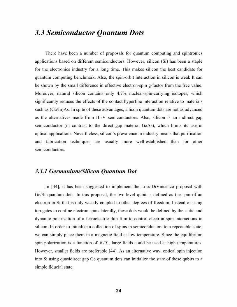
transduction, as in the tunneling scheme of Kane [48]. The design of this proposal is
depicted in Figure 6, which incorporates aspects of two existing types of quantum dots:
lateral tunneling dots and vertical tunneling dots.
Figure 6. (Color online) The two quantum-dot devices simulated in this paper. (a) A
double-dot structure. (b) A four-dot structure [Top view only; heterostructure
identical to (a)] [47].
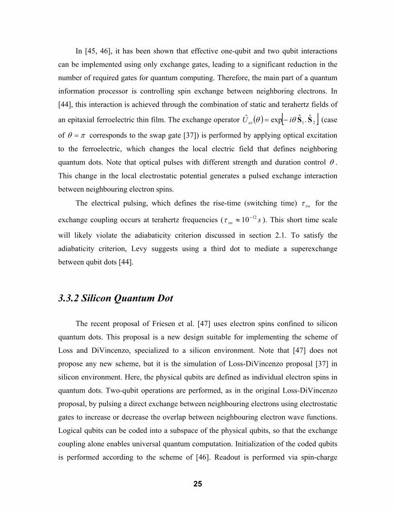
Stoneham et al. [49] introduced another quantum dot proposal based on exploiting
the properties of impurities in silicon. In this proposal, the qubits are the electron spins
bound to deep-donor impurities in silicon. The space between each pair of qubits ( )BA,
should be large enough such that the ground state interactions between donor spins are
small. Controlled optical excitation of a charge-transfer transition from a nearby control
impurity C promotes a ‘control’ electron from C into a molecular state of A and B . In
this excited state, there is an effective exchange interaction between the qubit spins.
Qubit–qubit interactions are switched on by optical excitation and off by stimulated de-
excitation of the control electron (see Figure 7).
In order to initialize qubits to all-zero state, the spin-polarized electrons are injected
into the material (magnetic initialization). Polarization-selective optical pumping is
another alternative way. Single-qubit gates are performed by ciombining confocal optics
and magnetic resonance [49]. In order to implement rwo-qubit gates, the control atom C

27
is excited to a suitable state. Therefore, the control electron wavefunction overlaps the
qubit states of A and B . Then, gates are manipulated by magnetic fields and optical light
pulses [49]. Since the energies involved in the gating process are large, Stoneham et al.
suggested that this proposal could potentially operate at the room temperature.
Figure 7. A schematic diagram of the quantum gate. The qubit spins are on deep
donors A and B (Ο ) with wavefunctions AW and BW . The control atom, C
(+ ), is the source of a control electron. In the ground state, the control electron is in
state CGW , whose wavefunction and potential well are shown schematically. In the
excited state, the control electron is in a charge-transfer, molecularlike, state, CEW ,
which overlaps both qubit electrons. Neither the qubits nor the control electron
interact significantly in the ground state, but interact causing entanglement in the
excited state [49].
3.4 Hybrid Quantum Dots
There have been several proposals for hybrid quantum computing, in order to
achieve the best features from different previous proposals (e.g. cavity QED, trapped ions
and trapped atoms) with the benefits offered by solid-state implementations of quantum
dots. In the following, we consider two hybrid proposals for quantum dots. The first one
28
is a quantum dot coupled with cavity QED [50] and the next one is a quantum dot
coupled with NMR [51].
3.4.1 Quantum Dot with Cavity QED
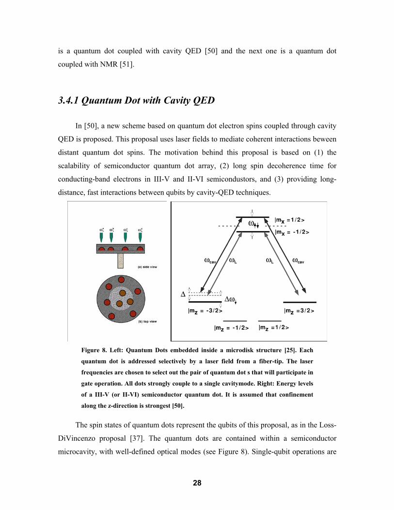
In [50], a new scheme based on quantum dot electron spins coupled through cavity
QED is proposed. This proposal uses laser fields to mediate coherent interactions beween
distant quantum dot spins. The motivation behind this proposal is based on (1) the
scalability of semiconductor quantum dot array, (2) long spin decoherence time for
conducting-band electrons in III-V and II-VI semicondustors, and (3) providing long-
distance, fast interactions between qubits by cavity-QED techniques.
Figure 8. Left: Quantum Dots embedded inside a microdisk structure [25]. Each
quantum dot is addressed selectively by a laser field from a fiber-tip. The laser
frequencies are chosen to select out the pair of quantum dot s that will participate in
gate operation. All dots strongly couple to a single cavitymode. Right: Energy levels
of a III-V (or II-VI) semiconductor quantum dot. It is assumed that confinement
along the z-direction is strongest [50].
The spin states of quantum dots represent the qubits of this proposal, as in the Loss-
DiVincenzo proposal [37]. The quantum dots are contained within a semiconductor
microcavity, with well-defined optical modes (see Figure 8). Single-qubit operations are

29
performed by applying two laser fields, polarized along the x and y directions, that
satisfy the Raman-resonance condition between ↓ and ↑ . The laser fields are excited
to create Raman r/π -pulse for the hole in the conduction band state. The non-parallel
components of the laser polarizations create a non-zero Raman coupling, resulting in
single-qubit rotations. To perform two-qubit operations, distant electron spins are coupled
via a delocalized cavity mode. This induces an xy -like interaction between electron
spins. In [50], it is shown that an xy -interaction and single qubit rotations are sufficient
to perform a two-qubit CNOT gate.
3.4.2 Hydrogenic Spin Quantum Dot
In the Hydrogenic Spin Quantum Computers, electron-nuclear spin pairs are
defined as qubits [51]. This model is a hybrid proposal between quantum dot and NMR
computing. In addition, this proposal uses the silicon-based solid state device, which is
the most promising feature of this proposal. Therefore, this proposal can also be
categorized in the silicon quantum dots.
This proposal relies on the encoding of each logical qubit in the 0=zJ subspace of
a pair of spins: ( ) 2/0 ↓↑−↑↓= and ( ) 2/1 ↓↑+↑↓= . Encoding often
results in reduced constraints on computer design [51]. It has been shown that [51] when
the two spins are an electron and its donor nuclear spin (a hydrogenic spin qubit) the
qubits are easier to control and can be coupled, well beyond their nearest neighbors, with
electron shuttling.
In this proposal, the electron and donor nuclear spins are coupled by the hyperfine
interaction. Changing the voltage on A gates modulates the electron and +P31 Donors.
With a high voltage, there is no coupling, since the electron is pulled toward the surface
of the silicon substrate. But with a low voltage, electrons strongly couple with +P31
donors. Coupling of the nuclei spin with the electron spin leads to the hyperfine
interaction. The nuclear spin interacts with the electron spins by dipole-dipole magnetic

30
interaction. As the result, the external magnetic field governs the Hamiltonian equation,
which describes the time-evolution of the electron and nuclear spins.
In order to perform the single qubit operation, the coupling between the electron
and donor nucleus is controlled such that the electron-nuclear paired qubit is rotated
through x axis. Then, applying the external static magnetic field rotates the paired qubit
through z axis.
Figure 9. Schematic of the proposed architecture. Each qubit is encoded in the spins of
an electron and its donor nucleus. ‘‘A gates’’ above donor sites switch the electron-
donor overlap, and thus the hyperfine interaction, while ‘‘S gates’’ shuttle electrons
from donor to donor. ‘‘Bit trains’’ of voltage pulses control the computer [51].
By electron shuttling between the adjacent A gates, the two-qubit operations can be
implemented. Note that S gates modulate this electron shuttling. This electron shuttling is
called Heisenberg interaction, which allows building two qubit gates [51] whose
combination can make a universal quantum gate.
By defining the unitary transformation
(30)
and
(31)
( ) h/, BBB TiHeB φφ −=
( ) ,, /hAAA TiHeA θθ −=
31
the CNOT operation is defined in [51] as
(32)
in which single-qubit operations
(33)
augment an entangler,
(34)
Note that ijA denotes the interaction between the ith electron and the jth donor.
( ) ( ) ,2121+⊗⊗= ZLNZLCNOT
( ) ,2
,2
,2
,2
3, 11221121
+
=⊗
ππππ BAAABZL
( ) .2
,2
3,,2
,2
3, 2112212112
+
+=
πππππ AABABAAN

32
Chapter 4
Experimental Implementation of Quantum Dots
At the beginning of the experimental section, we first review the technological
procedures to fabricate structures of various layers in nanometric sizes and monitor their
performance.
4.1 Fabrication Review
4.1.1 Molecular Beam Epitaxy (MBE)
Epitaxy is a high temperature process in an environment of the mixed chemicals,
which leads to deposit layers of a single crystal material on a single crystal substrate.
Temperature is applied to enable the reaction of chemical precursors. The deposited
material can be compound III-IV material like GaAs and the thickness varies in a huge
range, from 2 nm to over 11 µm. Basically, deposited layers follow the crystalline order
of the substrate crystal structure. Therefore, the substrate should be selected appropriately
for each application [52].

33
During Epitaxial film growth, the high process temperature can disturb the lower
layer profile. Therefore, a beam of molecules or atoms which radiate from evaporation or
effusion source can be used to sputter different atoms from different targets in an
evacuated chamber towards the substrate. This technique, which is called molecular beam
epitaxy (MBE) have to run in very low pressure ( 1110 1010 −− − Torr) environment to
ensure the minimum collision between the atom and air molecules and increase mean free
path (~ 10-10 cm).
Figure 10. (a) Schematic representation of MBE deposited of a three element film.
(b) Schematic cross-section of a MBE growth chamber for III-IV compound [52].
In another word, In MBE thin films crystallize via reactions between molecular or
atomic beams of the constituent elements and a substrate surface which is maintained at a
(b)
Substrate
Flux 1 Flux 2 Flux 3
Ultra High Vacuum
(a)

34
moderated elevated temperature in ultra high vacuum. This reduces the epitaxy process
temperature (450-800 oC), which is suitable for Quantum dot fabrication process. Figure
10.a shows a schematic representation of MBE deposition of a film with three elements.
The film thickness and composition is defined by controlling the individual fluxes [52].
Moreover, a schematic cross-section of a typical III-IV compound MBE growth chamber
is depicted in Figure 10.b.
4.1.2 Rapid Thermal Process
In fabrication processes it is usually required to diffuse atoms of one type among
atoms of substrate. This is used to obtain different profile concentration or contact metal
activation (sintering). But diffusion furnaces heat the sample up to temperatures of 800-
1100 oC to increase amount of diffusivity and thus decrease diffusion time. However, this
high temperature can out-diffuse the existing layers. It has been proved mathematically
that by decreasing the temperature ramping-up (heating) time, we can accelerate the
diffusion process and therefore obtain more abrupt structure [53].
Figure 11. Conceptual schematic of RTP chamber [53].
Rapid thermal annealing (RTA) uses bunch of special lamps for heating. These
lamps offer very fast ramp rates, up to 100 oC per second. Figure 11 shows a schematic
Substrate
Heating lamp elements
Gas in Gas out

35
for an RTA machine. In this system wafer rests on sharp pins or on a low thermal mass
holder to reduce wafer thermal loss. Thermal energy is delivered by optical energy
transfer between the radiating lamps and the substrate, so that the transparent walls of the
reaction chamber may remain relatively cool during short time processing. Finally it is
good to mention that the main issue in RTP process is the uniformity of the temperature
on the surface, which is worthy to study [53].
Another application of the RTA is to electrically activate the implanted atoms in the
substrate. In Quantum dot experiments this technique is used to fast diffuse and activate
the Gold/Titanium contact for quantum point contacts (QPC). Also it has been some
reports to fabricate Quantum dots with ion implantation and then using RTA to activate
the Quantum Dots.
4.1.3 Lithography
The most important cornerstone in micro- and nano-technology is lithography. This
technique is used to pattern tiny structures on the substrate. The idea behind this is
exactly same as the one for developing photos. First a light sensitive material called
photoresist is applied to the surface by spinning and is baked to become ready for
exposure. In fact, by heating some resins evaporates from the photoresist. After that, the
wafer is covered with mask and light is applied to the mask and wafer. The photoresist at
the parts covered by mask do not receive any photons, while the uncovered photoresist is
shined by light and the chemical polymer chain is broken. These broken polymers can be
cleared by specific liquid called developer. The result will be the patterned photoresist,
which is ready for further fabrication processes. In this time, the uncovered parts of the
wafer by photoresist can be exposed to any chemical to be etched.
A film can also be deposited on top of the wafer and photoresist. The next step is to
remove the photoresist, which can be easily done by putting the substrate into Acetone
bath. If we had done etching at the step before, the resulting wafer would be a wafer with
the part that is etched by the mask pattern. But if the process at step before was
deposition, the final result would be a wafer with the deposited tracks on top exactly as
the tracks on the mask. The latter process is called “lift-off” and is very interesting

36
technique to build free standing structures, which is extremely suitable for Quantum dots
[52, 53].
The big problem for performing lithography for smaller dimensioned is the wave
length of the light source. The visible light has resolution is more than 400 nm, which is
definitely not good for nanometric patterning. For micro-technology processes UV and
ultra deep UV beams are used (λ > 100nm), which is still not suitable for nano size
processes. Therefore, the energetic electron is a solution for this problem. The electron
beam lithography (EBL) uses electrons with the wave length of less than 0.1 nm. This
enables definition of patterns less than 10 nm. But the problem for EBL is that the entire
system and material, like photoresist and optical focus system, has to be re-designed.
Moreover, as it is only one ray of electron, the e-beam has to sweep on all over the
surface, which this reduce the speed and therefore yield of the process [52].
4.2 Characterization Review
4.2.1 Scanning Electron Microscopy (SEM)
Scanning Electron Microscope (SEM) is very powerful tool to observe micrograph
of microscopic objects. Essentially it uses electron beams instead of photons. Electrons
emitted from electron guns can get focused by some condensing lenses. These lenses are
acting like regular lenses but for electrons. After focusing electrons pass through a scan
coil and objective lens to get swept and focused more respectively to hit the target. The
output image is made by analyzing backscattering of secondary electrons. Therefore as
wave length of source electron decreases (energy increases) the smaller dimensions can
be detected. Basically pictures with the resolution of 100 nm are obtained by 30 KV
potential between electron gun and the sample. This requires the sample to be conductive
allowing it to hold a voltage [54]. Figure 12 depicts a sample SEM image from a
Quantum dot used for quantum computation [55].

37
Figure 12. SEM micrograph for a Quantum dot structure. The light areas are the
metal contacts [55].
4.2.2 Atomic Force Microscopy (AFM)
Atomic force microscopy (AFM) operates by measuring the forces between a
cantilever (probe) and the sample. This force actually depends on the nature of the
sample, the distance between the cantilever and the sample and its geometry, and sample
surface contamination. In contrast to SEM, AFM is suitable for both conductive and
insulating samples. Basically, the probe sweeps across the sample and record the force
(usually Van der Waals force) that relates with the distance between cantilever and
sample. So knowing the height of the cantilever, surface profile can be calculated [54].
Figure 13 shows a bundle of single walled carbon nanotubes to which electrical leads
have been patterned. Actually, carbon nanotubes (CNT), the extended cousins of C60,
have proven to be a system that can be understood using the ideas developed for dots.
The nanotube is predicted to act as a one-dimensional quantum wire, and a finite length
turns it into a one-dimensional quantum dot [55].
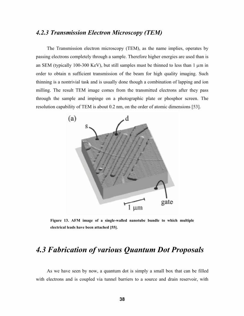
38
4.2.3 Transmission Electron Microscopy (TEM)
The Transmission electron microscopy (TEM), as the name implies, operates by
passing electrons completely through a sample. Therefore higher energies are used than is
an SEM (typically 100-300 KeV), but still samples must be thinned to less than 1 µm in
order to obtain n sufficient transmission of the beam for high quality imaging. Such
thinning is a nontrivial task and is usually done though a combination of lapping and ion
milling. The result TEM image comes from the transmitted electrons after they pass
through the sample and impinge on a photographic plate or phosphor screen. The
resolution capability of TEM is about 0.2 nm, on the order of atomic dimensions [53].
Figure 13. AFM image of a single-walled nanotube bundle to which multiple
electrical leads have been attached [55].
4.3 Fabrication of various Quantum Dot Proposals
As we have seen by now, a quantum dot is simply a small box that can be filled
with electrons and is coupled via tunnel barriers to a source and drain reservoir, with
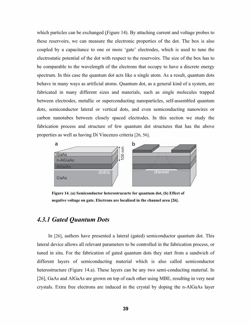
39
which particles can be exchanged (Figure 14). By attaching current and voltage probes to
these reservoirs, we can measure the electronic properties of the dot. The box is also
coupled by a capacitance to one or more ‘gate’ electrodes, which is used to tune the
electrostatic potential of the dot with respect to the reservoirs. The size of the box has to
be comparable to the wavelength of the electrons that occupy to have a discrete energy
spectrum. In this case the quantum dot acts like a single atom. As a result, quantum dots
behave in many ways as artificial atoms. Quantum dot, as a general kind of a system, are
fabricated in many different sizes and materials, such as single molecules trapped
between electrodes, metallic or superconducting nanoparticles, self-assembled quantum
dots, semiconductor lateral or vertical dots, and even semiconducting nanowires or
carbon nanotubes between closely spaced electrodes. In this section we study the
fabrication process and structure of few quantum dot structures that has the above
properties as well as having Di Vincenzo criteria [26, 56].
Figure 14. (a) Semiconductor heterostrucurte for quantum dot, (b) Effect of
negative voltage on gate. Electrons are localized in the channel area [26].
4.3.1 Gated Quantum Dots
In [26], authors have presented a lateral (gated) semiconductor quantum dot. This
lateral device allows all relevant parameters to be controlled in the fabrication process, or
tuned in situ. For the fabrication of gated quantum dots they start from a sandwich of
different layers of semiconducting material which is also called semiconductor
heterostructure (Figure 14.a). These layers can be any two semi-conducting material. In
[26], GaAs and AlGaAs are grown on top of each other using MBE, resulting in very neat
crystals. Extra free electrons are induced in the crystal by doping the n-AlGaAs layer

40
with Si. These electrons trapped at the interface between GaAs and AlGaAs, which is
approximately 100 nm below the surface. As a result they form a two- dimensional
electron gas (2DEG) – a thin (10 nm) sheet of electrons that can only move along the
interface. The 2DEG can have a high mobility and relatively low electron density
(typically 105−106 cm2/Vs and ~ 3×10¹⁵ m−2, respectively). The low electron density
results in a large Fermi wavelength (~ 40 nm) and a large screening length, which allows
us to locally deplete the 2DEG with an electric field. This electric field is created by
applying (negative) voltages to metal gate electrodes on top of the heterostructure (see
Figure 14) [26].
The fabrication begins with photoresist spinning of the heterostructure sample
surface (typically poly-methyl-methacrylate, PMMA) (Figure 15.a). Then the mask is
applied and the gate is patterned. Because of the very small dimension of the structure,
the electron is used for the optics (EBL) to obtain tiny spot sizes down to 20 nm. After
exposure and developing the resist, we will deposit the gate metal (5 nm Titanium plus 30
nm Gold) and then remove the resist as it was in lift-off process (Figure 15). Now metal
electrodes are left at the places that were exposed to the electron beam [26, 56].
Figure 15. Fabrication steps for the gate patterning, (a) Resist exposure by
electrons, (b) Development, (c) Metal evaporation, (d) Lift-off [26].
Figure 16 shows the final structure, which by applying negative voltages to the
gates the 2DEG is locally depleted, creating one or more small islands that are isolated
from the large 2DEG reservoirs. The actual quantum dots are located at these islands. In
order to probe them, we need to connect an electrical contact to the reservoirs. To do this,
we use rapid thermal annealing (RTA) to diffuse AuGeNi through the surface to the
2DEG level. This forms Ohmic contacts between the 2DEG source-drain reservoirs and
metal bonding pads on the surface. Metal wires bonded to these pads are used to flow the
current or apply voltage and their probing [26].

41
Figure 16. (a) Schematic of the lateral gated quantum dot device, (b) SEM image if
the fabricated gated quantum dot [26].
Figure 17. Few electron quantum dot devices made on GaAs/AlGaAs
heterostructure, 2-DEG is located 90 nm below the surface (a) SEM image (b) SEM
image (c) AFM image [26].

42
Also fabrication of several few-electron quantum dots has been reported. The
characteristic of each structure depends on the gate metal pattern, as well as the
semiconducting material properties. Figure 17 shows the picture of three different
quantum dots built by Elzerman et al [26].
Finally, it is good to note that except GaAs based quantum dot, some other
semiconductor material like InSb and Si also has been used. But still the dot diameter has
to be in order of 10 to 100 nm and they should typically be characterized by an electron
level spacing of 0.1 to 2 meV and charging energy of about 1 to 2 meV [39].
Another recipe for Quantum dots fabrication is to form them naturally at monolayer
steps at the interface of, e.g., thin GaAs/AlGaAs quantum wells. MBE is the most
common technological approach used for the growth of such systems. If the MBE growth
process is performed without interruption, such steps occur at random positions as natural
fluctuations of the quantum well width. This type of Quantum dot shows very excellent
optical properties, including very sharp optical line widths. This has allowed the coherent
control of optically excited states in the experiments and has recently terminated in the
implementation of a CNOT gate for qubits which are defined by the presence or absence
of an exciton in the quantum dot [39, 57].
4.3.2 Vertical Quantum Dots
Generally the idea behind quantum dot for quantum computation is to localize few
electrons into nano-sized structure and inspect the spin of them as quantum bit element.
In previous approach (gated quantum dot) electrical potential generates a potential well to
prevent electrons escaping from dot. Another alternative way for realization of the
coulomb blockage inside quantum dots is to make nano-sized free standing dot, and
watch for electron spin inside this dot. The etching techniques can be applied to obtain
lateral confinement in the plane of a 2DEG [19].
The vertical quantum dot reported by Tarucha et al is shown schematically in
Figure 18.a. It is made from a double-barrier heterostructure (DBS). By using a well-
defined heterostructure tunnel junction, the number of electrons in the dot can be
precisely changed one by one from 0 to more than 40 by changing the gate voltage. The

43
DBS consists of an undoped 12 nm In0.05Ga0.95As well and undoped Al0.22Ga0.78As
barriers of thickness 9 and 7.5 nm. The thinner layer is located closer to the substrate.
The source and drain contacts are made from n-type GaAs and are lightly doped close to
the DBS. The DBS is to form a mesa with top contact geometrical diameter D by using a
combined dry and wet etch to a point just below the DBS region. Furthermore, the
circular Schottky gate is placed on the side of the mesa close to the DBS. It is good to
note that the inclusion of In in the well reduces the bottom of the conduction band below
the Fermi level of the contacts. This allows us to study linear transport through a vertical
quantum dot. The current I flowing vertically through the dot is measured in response to a
small dc voltage applied between the contacts. Note that all the results are reproduced in
both polarities for the voltage, since the device is in the linear transport regime. The
electron temperature during the process is estimated to be about 0.2 K [22].
(a) (b)
Figure 18. (a) Schematic diagram of the DBS pillar structure quantum dot device.
The dot is located between the two heterostructure barriers [26, 22], (b) Schematic
of the TBS pillar structure quantum dot [58].
The same structure can also be fabricated as triple barrier structure (TBS). Figure
18 shows the schematic of the TBS device and its measurement setup. The triple barrier
structure (TBS) is consisting of three layers of Al0.22Ga0.78As and two layers of
In0.05Ga0.95As. A two-dimensional electron gas (2DEG) forms in the InGaAs layers. The
vertically (weakly) coupled double dot is formed by etching a submicron diameter pillar
out of the TBS. The Schottky diode gate wrapped around the pillar by applying a
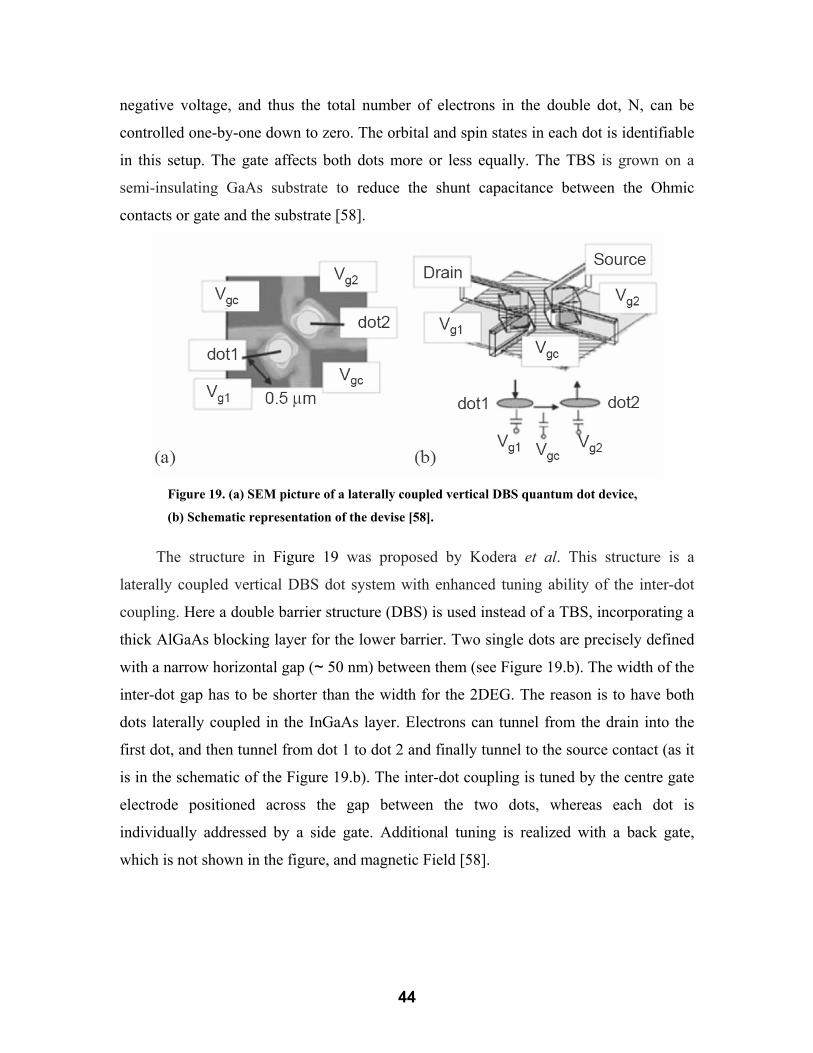
44
negative voltage, and thus the total number of electrons in the double dot, N, can be
controlled one-by-one down to zero. The orbital and spin states in each dot is identifiable
in this setup. The gate affects both dots more or less equally. The TBS is grown on a
semi-insulating GaAs substrate to reduce the shunt capacitance between the Ohmic
contacts or gate and the substrate [58].
Figure 19. (a) SEM picture of a laterally coupled vertical DBS quantum dot device,
(b) Schematic representation of the devise [58].
The structure in Figure 19 was proposed by Kodera et al. This structure is a
laterally coupled vertical DBS dot system with enhanced tuning ability of the inter-dot
coupling. Here a double barrier structure (DBS) is used instead of a TBS, incorporating a
thick AlGaAs blocking layer for the lower barrier. Two single dots are precisely defined
with a narrow horizontal gap (~ 50 nm) between them (see Figure 19.b). The width of the
inter-dot gap has to be shorter than the width for the 2DEG. The reason is to have both
dots laterally coupled in the InGaAs layer. Electrons can tunnel from the drain into the
first dot, and then tunnel from dot 1 to dot 2 and finally tunnel to the source contact (as it
is in the schematic of the Figure 19.b). The inter-dot coupling is tuned by the centre gate
electrode positioned across the gap between the two dots, whereas each dot is
individually addressed by a side gate. Additional tuning is realized with a back gate,
which is not shown in the figure, and magnetic Field [58].

45
4.3.3 Self-Assembled Quantum Dots
Another approach to fabricate nano-sized quantum dot structures is to grow them
using self-assembly, which is based on the Stranski-Krastanov growth technique. In this
technique, self-assembled dot islands develop spontaneously during epitaxial growth due
to a lattice mismatch between the dot and the substrate material [59]. Leonard et al have
used the 2D-3D growth mode transition during the initial stages of growth of highly
strained InGaAs on GaAs to obtain quantum-sized dot structures. More structural study
has also revealed that if the growth of In0.5Ga0.5As is interrupted exactly at the onset of
this 2D-3D transition, dislocation-free dots of the InGaAs are produced. The size of these
dots are in around 300 Ǻ in diameter and remarkably uniform to within 10% of this
average size. Generally, the luminescent intensities of these dots are greater than or equal
to those of the underlying reference quantum wells [59].
Typical sets of dot/substrate material for self assembled grown samples are
InAs/GaAs, Ge/Si(100), GaN/AlN, InP/GaInP, and CdSe/ZnSe [60]. The electron level
spacing of this type of dot is typically around 30 to 50 meV with a charging energy of 20
meV, a diameter size 10 to 50 nm, and a height of 2 to 10 nm of the dot, which has higher
energies comparing to typical gated quantum dots [39]. Figure 20 shows AFM picture of
dots grown at random locations. Small self-assembled dots typically have a pyramidal
shape with four facets, whereas larger dots (containing, e.g., 7 InAs monolayer) form
multi-faceted domes [60].
Figure 20. AFM picture of self-assembled InAs quantum dot structure [59].

46
Figure 21. TEM cross-section of vertically stacked dots, ordered along the growth
axis [39].
In some cases the pyramidal self-assembled dots are covered with a thin layer of the
substrate material, which is called the capping layer. The capped dots have usually an
elliptical or rarely even a circular shape. Furthermore, these dots exert strain on the
capping layer. Now if we grow quantum dots on the top of capping layer, they tend to
grow on the strain field on top of the capped dots rather than at random positions. This
enables the growth of vertically coupled quantum dots, where the thin capping layer acts
as a barrier between the two dots. Figure 21 depicts a TEM cross section of such layers.
As it is observed in Figure 20, we know that for a typical Stranski-Krastanov self-
assembled dots the randomness is inherent nature of the process. Therefore, pre-
patterning of the substrate has been found to be a way to achieve a well-defined growth
position of the first dot layer [61]. Very well-ordered atom configuration in Figure 22
illustrates the result of this technique.
Figure 22. AFM picture of laterally ordered quantum dots grown on pre-patterned
substrate with a 20 nm In0.2Ga0.8As layer to generate stress [61].

47
Another trick to organize the growth site of single and coupled dots over substrate
is to use by Cleaved-edge overgrowth technique [62]. Colloidal chemistry is yet another
promising approach to assemble quantum dots with well-controlled size and shape [63].
Recently, colloidal CdSe dots have been coupled via molecular bridges [64].
4.4 Spin Quantum Dot Read-Out Techniques
As we discussed earlier, the electron spin is used to represent qubits. In this section
we focused on the electron spin measurement techniques inside the quantum dots. We
know that two different spins are distinguishable by their magnetic moment. Therefore,
the idea behind measurement is to apply appropriate magnetic field (~ 10 T), according to
Zeeman energy, and observe the split of different spins, which can be either parallel or
anti parallel to the applied field. In this case the thermal energy has to be very lower than
magnetic moment energy difference. Therefore, all measurements have to be done at very
low temperature, ~mK. The separated spins has fallen into different energy states and can
be detected by various techniques such as optical techniques [65], magnetic resonance
force microscopy [66, 67], and electrical read-out [26, 68, 69]. Here, we more focus on
the electrical techniques introduced in [26]. The structure shown in Figure 23 is discussed
based on the electrical signals applied to each electrode and correspondent measurement.
Figure 23. SEM micrograph of the double dot structure with quantum point contact
(QPC) on the drain and source side. The tunneling of electrons is controlled with the
electrode’s voltage [26].

48
The charge on the dot is been detected by measuring the current of the quantum
point contact (QPC) [44, 45]. First to demonstrate this functionality, only the left dot dot
and QPC is functioned. This can be achieved by grounding gates R and PR, and in a
mean time use the left QPC as a charge detector. The QPC is created by applying
negative voltages to Q − L and L. This confines the 2DEG with a conductance, G, which
is quantized when sweeping the gate voltage VQ−L. The last area of little variation (at G =
2e2/h) and the transition to complete pinch-off (i.e. G = 0) are shown in Figure 24. Based
on this figure the QPC can be biased in the region with highest conductance sensitivity
(G ≈ e2/h) [26].
Figure 24. QPC current versus gate voltage VM. Arrows show the voltages where
electrons escape the dot. By increasing amount of VM number of electrons at dot
increases [26].
By reducing amount of the gate voltage, VM, the number of electrons in the left dot
is changed (decreased). This also reduces the QPC current, which is due to the capacitive
coupling from the gate M to the QPC. By changing number of charges in the dot the
electrostatic potential at the QPC region suddenly change and this lead to a step-like
feature in IQPC (see Figure 24). In another word this step confirms a change in the electron
number. So, even without passing current through the dot, IQPC provides information
about the charge variation on the dot. It is also good to note that the electrons can be
pushed out by changing gate voltage periodically. To further charge sensitivity
enhancement it is shown that a small modulation (0.3 mV at 17.7 Hz) can be applied to

49
VM and dIQPC/dVM measurement [70]. The sensitivity of the charge detector is estimated
to be about 0.1e, where e is the single electron charge [26]. The unique advantage of QPC
charge detection is that it provides a signal even when the tunnel barriers of the dot are so
opaque that IDOT is too small to be measured [70]. This allows us to study quantum dots
even when they are virtually isolated from the reservoirs.
Figure 25. dIQPC/dVL versus VL and VPR, showing charge configuration of the double
quantum dot. Dark lines notify a peak in dIQPC/dVL, corresponding to a change in
the total number of electrons on the double dot [26].
Now let’s consider a case that electrons can exist in both dots of the Figure 23. The
same as the single dot operation, here the QPC can also detect changes in the charge
configuration of the double dot. This can be achieved by measuring dIQPC/dVL versus VL
and VPR for the right-hand QPC, Figure 25. In this case VL mainly controls the number of
electrons on the left dot, and VPR that on the right. Together these lines form the so-called
‘honeycomb diagram’. The more horizontal lines attributed to a change in the number of
electrons on the left dot, whereas almost-vertical lines indicate a change in the electron
number on the right. As it is observed in the Figure 25 in the upper left region (smaller

50
VL part) the ‘horizontal’ lines are not present, even though the QPC can still detect
changes in the charge, as demonstrated by the presence of the ‘vertical’ lines. Elzermann
et al conclude that in this region the left dot contains zero electrons. This is based on the
fact that by reducing voltage no more electrons escape. Moreover for the right hand dot
there is the same story about disappearance of the ‘vertical’ lines, which occurs in the
lower right region. Combining these two conclusions we can see that in the upper right
region the absence of lines shows that here the double dot is completely empty [26].
Now by increasing amount of both voltages we can track exact number of electrons
in each dot from the honey comb structure, as it is labeled in Figure 25. This can be done
by simply counting the number of ‘horizontal’ and ‘vertical’ lines that separate it from
the 00 region. For example label ‘12’ means 1 electron in the left dot and 2 electrons on
the right. The point, where 01 switches with 10, represents transfer of one electron from
right dot to the left. This fact is initialed because of the electron tunneling between two
dots. The light lines in Figure 25 indicate the transfer of one electron from one dot to
another by tunneling. Rate of tunneling can be controlled with the amount of the voltage
on gate M, VM. The less VM is, the higher barrier exists between two dots, and thus less
tunneling occurs, Figure 26. Finally it is good to note that the visibility of all lines in the
honeycomb pattern demonstrates that the QPC is sufficiently sensitive to detect even
inter-dot transitions [26]. Figure 26.a (weak-coupling regime) shows the familiar
honeycomb diagram in the few-electron regime. All lines indicating charge transitions are
very bold and straight, indicating that for the used gate voltages, the tunnel-coupling
between the two dots is negligible compared to the capacitive coupling. By making VM
less negative, the tunnel barrier between the two dots is made more transparent, until the
inter-dot tunnel-coupling becomes comparable to the capacitive coupling. In Figure 26.b,
the inter-dot coupling dominates over capacitive coupling, by making VM even less
negative. This regime is so-called the strong-coupling regime. In this case, all lines are
much curved, implying that the tunnel-coupling is dominating over the capacitive
coupling. In this regime, as there is no strong barrier between two dots they are both
combined and the double dot behaves like a single dot [26]. It is also shown that this
tunneling can be assisted by photon exposure [26].

51
(a) (b)
Figure 26. Controlling the inter-dot coupling with VM, small modulation is applied
to VPR (3mV and 235 Hz); magnetic field of 6T is applied at the 2DEG plane (a)
Weak coupling regime, (b) Strong coupling regime VM=0.1V [26].
By now, we only found out that how many electrons exist inside single and double
quantum dots. But as we know, electrons can have parallel or anti parallel spins. Now
let’s investigate the approaches to determine these spins. Figure 27.b shows the device
which we measure its electron spin. In this case reservoir acts as the second quantum dot
and Γ is trimmed by VM. In this case metallic gates are lied on the surface of a
GaAs/Al0.27Ga0.73As heterostructure containing a 2DEG 90 nm below the surface. The
electron density is 2.9 × 10¹⁵ m−2 [26, 71]. The tunnel barrier between gates R and T are
made sufficiently opaque to completely isolate the dot from the drain contact on the right.
The barrier to the reservoir on the left is set to a tunnel rate Γ ≈ (0.05 ms)−1. By tunneling
on or off the dot, electrons change the electrostatic potential in its vicinity, including the
region of the nearby QPC (defined by R and Q). The QPC is also biased in the tunneling
mode to have very sensitive IQPC. By this setup, the QPC acts as a charge detector with a
resolution much better than a single electron charge and a measurement timescale almost
ten times shorter than 1/Γ [26].

52
Figure 27. Spin-to-charge conversion in a quantum dot coupled to a QPC a)
Principle of spin-to-charge conversion. The charge on the quantum dot remains
constant if the electron spin is ↑, whereas a spin-↓ electron can escape. b) SEM of the
metallic gates [71].
As we have mentioned before, the thermal energy of electrons (3/2 kT) has to be
less than Zeeman energy difference, so she device is placed inside a dilution refrigerator
down to 10mK. Moreover, a magnetic field of 10 T in the plane of the 2DEG is applied.
By this magnetic field two spin energies are separated by the Zeeman splitting in the dot
of about ∆EZ ≈ 200µeV. This amount is larger than the thermal energy (25 µeV) but
smaller than the orbital energy level spacing (1.1 meV) and the charging energy (2.5
meV). In this regime the spin with higher energy (down arrow) overcomes the barrier,
Γ,and leaves the dot to reservoir, but the spin with lower energy (up arrow) remains on
the dot, Figure 27. Therefore, by inspecting IQPC, we can determine if there is any
electron remained in dot or not. Having electron in dot indicates downward spin, and lack
of electron specifies the upward spin electron [71]. Interesting point is that as we have
entered considerable amount of energy to system, by measuring the spin (qubit) its
quantum state changes. This confirms the fact of not having qubit cloning.
The spin measurement technique has based on three major procedures: (1) empty
the dot, (2) inject one electron with unknown spin, and (3) measure its spin state. The
different stages are controlled by voltage pulses on gate P (Figure 28.a), which shift the
dot’s energy levels (Figure 28.c). The pulse level is 10 mV during twait and 5mV during tread,
which is 0.5 ms for all measurements.

53
Figure 28. Two-level pulse technique used to inject a single electron and measure its
spin orientation, a) Shape of the voltage pulse applied to gate P, b) Schematic QPC
pulse-response if the injected electron has spin ↑ (solid line) or spin↓ (dotted line).
The difference between dotted and solid line is only seen during the read-out stage,
c) Schematic energy diagrams for spin↑ (E↑) and spin↓ (E↓) during the different
stages of the pulse [71].
Assume before the pulse the dot is empty, thus both up↑ and down↓ spins are
located above the Fermi energy of the reservoir, EF. The voltage pulse pulls both levels
below EF. Now energetic enough electrons can tunnel into the dot. By average this
happens after time of Γ−1 sec. The particular electron can have spin-↑ (shown in the lower
diagram) or spin-↓ (upper diagram). It is good to note that the tunnel rate for spin-↑
electrons is little larger than that for spin-↓ electrons (Γ↑ > Γ↓). As it is shown in Figure
28, during twait the electron is trapped on the dot and consequently Coulomb blockade
prevents a second electron to be added. We observe a little fall in the ∆IQPC signal after
entering the electron into the dot, which is due to its electrostatic energy and its effect on
QPC. After twait the pulse is reduced, in order to position the energy levels in the read-out
54
configuration. If the electron spin is ↑, its energy level is below EF, so the electron
remains on the dot. If the spin is ↓, its energy level is above EF, so the electron tunnels to
the reservoir after a typical time ~Γ↓−1. This has assumed that Γ = Γ↑ + Γ↓. Now
Coulomb blockade is lifted and an electron with spin-↑ can tunnel onto the dot. This
occurs on a timescale ~Γ↑−1. After tread, the pulse ends and the dot is emptied again. The
expected QPC response, ∆IQPC, to such a two-level pulse is the sum of two contributions
(see Figure 28.b). First, due to a capacitive coupling between pulse-gate and QPC, ∆IQPC
will change proportionally to the pulse amplitude. Thus, ∆IQPC versus time resembles a
two-level pulse. Second, ∆IQPC tracks the charge on the dot, i.e. it goes up whenever an
electron tunnels off the dot, and it goes down by the same amount when an electron
tunnels on the dot. Therefore, if the dot contains a spin-↓ electron at the start of the read-
out stage, ∆IQPC should go up and then down again. We thus expect a characteristic step
in ∆IQPC during tread for spin-↓ (dotted trace inside gray circle). In contrast, ∆IQPC should
be flat during tread for a spin-↑ electron. Measuring whether a step is present or absent
during the read-out stage constitutes our spin measurement [71].
4.5 Quantum Dot Initialization
Initialization of the spin to the pure state ↑ is the desired initial state for most
quantum algorithms [1]. Due to low coherency time of the quantum states and the fact
that the state ↑ has less energy, it has been confirmed that by waiting long enough at the
presence of magnetic field (gµBB > 5kBT), energy relaxation will cause the spin on the
dot to relax to the ground state ↑ , Figure 29.a. Although this method is very simple and
robust initialization approach, it takes about 5T1 (T1 is spin relaxation time) to reach
equilibrium. This time usually last more than 10 ms, especially at lower magnetic fields,
where the spin relaxation time, T1, might be very long [26].

55
Figure 29.b shows the schematic energy diagram for a faster initialization method.
In this method the ‘reverse pulse’ technique has been used, as it was used for spin read-
out. By placing the dot in the read-out configuration, a spin-up electron will stay on the
dot, whereas a spin-down electron will be replaced by a spin-up. After waiting a few
times the sum of the typical tunnel times for spin-up and spin-down (~ 1/Γ↑ +1/Γ↓), the
spin will be with large probability in the ↑ state. This initialization procedure can
therefore be quite fast (< 1 ms), depending on the tunnel rates [26].
Figure 29. Schematic energy diagrams depicting initialization procedures in a large
parallel or perpendicular magnetic field, a) Spin relaxation to pure state, ↑ , b)
The ‘read-out’ configuration can result in ↑ faster initialization, c) Random spin
injection gives a statistical mixture of ↑ and ↓ , d) In a large perpendicular field
providing a strong spin-selectivity, injection results mostly in ↑ [26].
We also have the possibility to initialize the dot to a mixed state, where the spin is
probabilistically in either ↑ or ↓ . Mixed-state initialization can be demonstrated in a
parallel field by first emptying the dot, followed by placing both spin levels below EF
during the ‘injection stage’ (Figure 29.c). The dot is then randomly filled with either a
spin-up or a spin-down electron. This is very useful, e.g. to test two-spin operations. In a
large perpendicular field providing a strong spin-selectivity, initialization to the ↑ state
is possible via spin relaxation (Figure 29.a) or via direct injection (Figure 29.d).
Initialization to a mixed state (or in fact to any state other than ↑ ) is very difficult due to
the spin-selectivity. It probably requires the ability to coherently rotate the spin from ↑
to ↓ [26].
56
Chapter 5
Quantum Computing Problems in Quantum Dots
Several major obstacles to quantum dot quantum computation were identified and
addressed in the original work of Loss and DiVincenzo [37]. These obstacles include
entanglement (the creation and transport of a coherent superposition of states), gating
error (leakage to higher states outside of the qubit basis during gate operation), and
perhaps most importantly, coherence (the preservation of any given superposition in the
presence of a coupling to the environment). In the rest of this section, we review work
that has been done to understand and possibly overcome these obstacles in the context of
the Loss- DiVincenzo proposal [37].
5.1 Flying Qubits and Entanglement
In addition to DiVincenzo conditions for quantum computation stated in the
introductory section 1.4, there are two desiderata which are important for performing
quantum communication tasks [16]: (1) The ability to inter-convert stationary and flying
qubits. (2) The ability to faithfully transmit flying qubits between distant locations.

57
The whimsical term “flying qubits” refers to qubits that can be conveniently moved
from place to place [39]. The most obvious choice for a flying qubit is provided by the
polarization states of photons. In the context of quantum dot quantum computing, this has
led to a number of proposals for the conversion of quantum information or entanglement
from spin to light and vice versa. More recent work has suggested that free electron
quantum computation may be possible in principle in which mobile electrons (in some
material) travelling between dots could replace photons as the flying qubit medium of
choice.
The creation of nonlocal entanglement is deeply connected to the implementation of
flying qubits. The race to create and measure entangled particle pairs has led to a virtual
industry of so-called entangler proposals for the spin and orbital degrees of freedom. The
final goal of these proposals is generating and spatially separating a many-particle
quantum superposition that can be factorized into single-particle states. The canonical
example of such a state for the spin degree of freedom is the singlet formed from two
spin ½ particles: 2/)( ↓↑−↑↓ . The various effort related to spin entanglement
include proposals to extract and separate spin-singlet pairs from a superconductor
through two quantum dots or Luttinger liquid leads and proposals that generate
entanglement near a magnetic impurity, through a single dot , from biexcitons in double
quantum dots, through a triplet dot, and from Coulomb scattering in a two dimensional
electron gas [39]. Entanglement generation and measurement remains a lofty goal for
those working on solid-state quantum computing, theorists and experimentalists alike.
Recent experiments that have measured the concurrence (an entanglement measure) for
electrons in the ground state of a two-electron quantum dot point to a promising future
for entanglement-related phenomena in the solid state.
5.2 Decoherence
A fundamental problem in quantum physics is the issue of the decoherence of
quantum systems and the transition between quantum and classical behaviour. Of course

58
a lot of attention has been devoted in fundamental mesoscopic research to characterizing
and understanding the decoherence of electrons in small structures. A lot of studies has
been done on the orbital coherence of electron states, that is the preservation of the
relative
Phase of superposition of spatial states of electron. The coherence times seen in
these investigations are almost completely irrelevant to the spin coherence times which
are important in the quantum computer proposals. There is some relation between the
two, if there are strong spin-orbit effects, but the main intention is that conditions and
materials should be chosen such that these effects are weak.
Under these circumstances the spin coherence times (the time over which the phase
of a superposition of spin-up and spin-down states is well-defined) can be completely
different from the charge coherence times(a few nanoseconds), and in fact it is known
that they can be orders of magnitude longer. This is actually one of the main motivations
to propose spin rather than charge as the qubit. Here comes a brief description of the
experimental measurement of this kind of decoherence.
In magneto-optical experiments, based on time-resolved Faraday rotation
measurements, long spin coherence times were found in doped GaAs in the bulk and a
2DEG. At vanishing magnetic fields and T=5K, a transverse spin lifetime (decoherence
time) *2T exceeding 100ns was measured, with experimental indications that this time is a
single spin effect. Since this number still includes inhomogeneous effects – e.g. g-factor
variations in the material, leading to spins rotating with slightly different frequencies and
thus reducing the total magnetization – it represents only a lower bound of the transverse
lifetime of a single spin, *22 TT ≥ , which is relevant for using spins as qubits. Using the
same technique spin lifetimes in semiconductor quantum dots has been measured with at
most one spin per dot. The relatively small *2T decoherence times (a few ns at vanishing
magnetic field), which have been seen in these experiments, probably originate from a
large inhomogeneous broadening due to a strong variation of g-factor. Nevertheless the
fact that many coherent oscillations were observed provides strong experimental support
to the idea of using electron spin as qubits.
Since none of the experiments have been done on an actual quantum computing
structure, the existing result can not be viewed as conclusive. Because of sensitivity to

59
details, theory can only give general guidance about the mechanisms and dependencies to
be looked for, but can not make reliable a priori predictions of the decoherence times.
In fact there are further complications. We know theoretically that decoherence is
not actually fully characterized by a single rate; in fact, a whole set of numbers is needed
to fully characterize the decoherence process and no experiment has been set up yet to
completely measure this set of parameters, although the theory of these measurements is
available. There is a fact that every experimental apparatus shows some small fluctuations in
electrostatic voltage and applied magnetic field. Besides causing noise in measurement
these fluctuations, acting on an electron spin in a quantum dot, will inevitably induce
decay of the spin directly through the Zeeman interaction (in the case of a fluctuating
magnetic field), or indirectly through spin-orbit coupling (in the case of a fluctuating
electric field). The effect of these fluctuations can be treated accurately (for a week
coupling to the electron spin) by the phenomenological spin-boson model within a Born-
Markov approximation [72]. The coupling of the electron spin to the bath can not always
be treated as weak and effects of the bath memory (non-Markovian evolution) may be
important for achieving the level of accuracy required to perform quantum error
correction. For these reasons, the solution to this model has been extended to obtain non-
Mrkovian effects [73] and corrections beyond the Born approximation in the case of
ohmic dissipation in the bath.
Table 1 Relevant energy scales for the Loss-DiVincenzo quantum computing
proposal. The above estimates are based on a GaAs dot of lateral size l=30nm
containing N=105 nuclear spins. Correlation time is 10-4s [39].

60
Fluctuations in the voltage and magnetic field are artefacts of a given experimental
apparatus. In principle, these fluctuations can be reduced with improved electronics, and
can therefore be regarded as extrinsic sources of decoherence. In addition to these
extrinsic source, there are sources of decoherence that are intrinsic to the quantum dot
qubit design. These include the coupling of the electronic spin to the phonons in the
surrounding lattice or other fluctuations via the spin-orbit interaction and coupling of the
electron spin to surrounding nuclear spins via the contact hyperfine interaction. A
detailed understanding of the electron spin evolution under the influence of these
interactions is of fundamental interest and is necessary to implement reliable quantum dot
quantum computation. The first step to understanding any decoherence mechanism is to
estimate its size. In Table 1, an estimate for various energy scales related to decoherence
and qubit operation in the Loss-DiVincenzo proposal is given [39].
5.3 Spin-Orbit Coupling
We would like to assess the spin-orbit coupling strength for typical quantum dots.
Performing the standard non-relativistic expansion and reduction to a two-component
spinor for a Dirac electron to leading order in 2/1 mc leads to the spin-orbit coupling term
(35)
In the above equation, m is the electron mass, c is the speed of light, V(r) is the potential
experienced by the electron, P is the momentum operator in three dimensions, and S is
the electron spin operator. For a spherically symmetric parabolic confining potential,
( ) 2/220 rmV ω=r , the spin-orbit coupling term is ( ) S.L22
0 2/ mcH so ω= . Here,
PrL ×= is the orbital angular momentum operator, which can be substituted with h for
estimation purposes. Comparing the strength of this coupling to the orbital energy
meV1~0ωh gives 70 10~/ −ωhsoH [28]. This smallness of the spin-orbit coupling
compared to the orbital energy scale would suggest that the electron spin in quantum dots
is relatively free from external influences that couple to its charge. In realistic dots,
( )( ) SPr .2 22 ×∇= V
cmH so
h

61
however the confining potential is neither smooth (it has a r/1 singularity at the center of
each lattice ion), nor spherically symmetric, and the resulting spin-orbit interaction takes-
on a more complicated form. In a crystalline solid, the spin-orbit interaction is the sum of
structure inversion asymmetry and bulk inversion asymmetry terms, which can be written
for an electron confined to two dimensions as [39]
(36)
( )yx pp ,=p is the electron momentum operator in the x-y plane, and yx σσ and are the
usual Pauli matrices. For a strongly two dimensional system, the cubic term can be
neglected relative to the two first terms, which have the size 2,~ zyx pp . In a two
dimensional quantum dots, we replace lpdp yxz /,/ , hh ≈≈ , where d is the 2DEG
thickness and l is the lateral quantum dot size. The cubic term is then smaller than the two
linear terms by a factor of order ~ (d/l)2. The first two term coefficients have been
extracted from magneto resistance data in a GaAs/AlGaAs 2DEG. This gives the value o
h A4 −= meVβ and o
h A5 −−= meVα . To estimate the size of soH , given in (36), for a
quantum dot containing a single electron, we replace the momenta by lp yx /, h≈ where
l=10-100nm. This gives the range meVH so12 1010 −− −= [39]. This estimate is
significantly larger than the value ( meV710~ − ) for a simple parabolic confining
potential. All is not lost, however, since the spin-orbit coupling can only affect the spin
indirectly through fluctuations in the orbital degree of freedom. We can only assess the
real danger of this interaction through a correct microscopic analysis of the spin-orbit
Hamiltonian in the proper context.
The direct effects that a realistic spin-orbit interaction has on two-qubit gating
operations in a quantum computer have been explored by several authors. It has been
shown that the effect of the spin-orbit interaction on coupled quantum dot qubits can be
minimized by using time-symmetric qubit gating. Subsequently, Burkard and Loss [74]
have shown that the spin-orbit effect during gating can be eliminated completely for
appropriately chosen exchange pulse shaped. Additionally there have been several
investigations into the possible spin-flip (relaxation) and decoherence mechanism
mediated by the spin-orbit interaction and coupling to lattice phonons or other
( ) ( ) ( ).3pOppppH yyxxxyyxso ++−+−= σσβσσα

62
fluctuations. In many ways, an electron in the orbital ground state of a quantum dot is
very similar to an electron bound to a donor impurity site.
The rates of spin-flip transitions due to the spin-orbit interaction can be calculated,
both through direct relaxation from an excited orbital state accompanied by a spin-flip
and through a virtual process between the two states of a Zeeman-split doublet within the
same orbital state. The most effective spin-flip mechanism for a transition between
Zeeman- split states, which has a rate ( ) ( )40
51 //1 ωµ hBgT B∝ , is significantly reduced
for decreasing magnetic field B and increasing orbital energy 0ωh .
In the presence of spin-orbit coupling, a processing spin induces an oscillating
electric field. It has been suggested that this coupling may be a double-edged sword in
view of applications to spintronics [75]. On the positive side, the time-varying electric
field might provide access to the dynamics of a single isolated spin. The reverse
mechanism, however, leads to a further channel for spin relaxation from excitation in the
dot leads.
There have been further studies of spin-lattice relaxation mechanisms that are
specialized to particular quantum dot architectures. Some measurements has been done
on Si quantum dots and donor impurities [76] and a numerical exact-diagonalization
study has been done on GaAs quantum dots [77], extending the validity of previous
calculations to a more realistic set of wave functions.
The spin-flip relaxation time 1T is important for applications of spintronics
involving classical information, encoded in the states up and down. However, for
quantum computing tasks, the relevant time scale is the spin decoherence time T2, which
is the lifetime for a coherent superposition ↓+↑ ba . Typically, the decoherence time
is much less than the relaxation time ( 12 TT << ). The fluctuations induced from spin-orbit
coupling are purely transverse to the direction of an applied magnetic field to leading
order in the coupling. Because the fluctuations are purely transverse, the corresponding
2T time due to the combined spin-orbit and electron-phonon interactions exceeds the
value of the longitudinal spin relaxation time, given 12 2TT = . Moreover, for phonons in
three dimension, the spectral function is super-ohmic ( 3~ ω ) and thus the pure dephasing
63
contribution is absent, again ensuring that 12 2TT = . provided other decoherence
mechanisms can be arbitrarily suppressed, this result is very promising for applications of
quantum dot quantum computing in view of recent experiments that show exceptionally
long 1T times for single electron spins confined to GaAs quantum dots.
5.4 Spin-Spin Coupling
Unfortunately the spin-orbit interaction is not the end of the decoherence story. The
electron spin can also couple directly to other spins embedded in the quantum computer
device. In a GaAs quantum dot, the electron wave function contains approximately 510=N lattice nuclei, and every nucleus carries spin 2/3=I . The dominant spin-spin
coupling for this type of dot arises from the Fermi contact hyperfine interaction. The
Fermi contact hyperfine interaction for an electron with orbital envelope wave function
( )rψ and spin operator S interacting with surrounding nuclear spins kI is described by
the spin Hamiltonian
(37)
Here, 0v is the volume of a crystal unit cell containing one nuclear spin. Due to hfH , the
electron spin will experience an effective magnetic field (the Overhauser field ), which
gives rise to an energy splitting on the order of pI A, where I is the total nuclear spin
system, the Overhauser field includes a splitting meVI -110A =≈ in GaAs. In a typical
unpolarized sample, we have Np /1≈ , which gives a splitting meVNIA 410/ −≈ for
a quantum dot containing 510=N nuclear spins. In addition, the nuclear spin at site k
will experience an effective Zeeman splitting (Knight shift) on the order of
meVNAAk610/ −=≈ near the dot center to 0=kA far from the dot; nuclear spins at
different sites will process with different frequencies. This dispersion in the Knight shift
will effectively destroy collective states generated in the nuclear spin system on a time
∑=k
kkhf AH ,. IS
( ) .20 kk AvA rψ=

64
scale sNt µ1~h≈ [39], and is therefore important for proposals based on nuclear spin
quantum computing.
In addition to the Fermi contact hyperfine term, there is an anisotropic contribution
to the hyperfine interaction. For a widely separated electron and nucleus, the anisotropic
hyperfine interaction reduces to the interaction energy between point dipoles:
(38)
where the sum is over k.
If the electron spin is in a spherically symmetric orbital s-state with the nuclear spin
at its center, the anisotropic hyperfine interaction vanishes identically. The contribution
of this term from nuclear spins near the dot center will therefore be small, but for nuclear
spins near the edge of the electron wave function, which do not see a spherical electron,
spin distribution, it may become appreciable. Assuming approximately 510=N nuclear
spin have a significant dipolar coupling to the electron, we estimate the size of the
electron-nuclear dipolar interaction as meVlNH BNdd73 10/ −≅≈ µµ , where nml 30=
is the typical dot size.
The final spin-spin coupling directly associated with the electron is the magnetic
dipolar coupling of the electron to other electron spins in neighboring quantum dots. This
can be estimated as .10/ 932 meVlB−≈µ Although this coupling is very weak for
neighboring single-electron quantum dots it can become significant at atomic length
scales, and may be a significant source of decoherence for other solid-state proposals
[43]. In addition to direct electron spin coupling mechanisms, there are also significant
mechanisms that couple the environment to itself. For example, the nuclear spin
experiences a mutual dipolar coupling. This dipolar coupling causes the nuclear
environment to evolve dynamically, which can, in turn, affect the electron through direct
hyperfine coupling. The nuclear spins evolve on a time scale given by the dipolar
correlation time sdd410−=τ . The time ddτ is determined from the line width of the
NMR resonance in bulk through meVdd810/ −≅τh .
There have been many studies of electron spin dynamics in the presence of the
strongest (Fermi contact hyperfine) spin-spin interaction. In [28], it has been showed that
in the presence of the hyperfine interaction with surrounding nuclear spins, the electron
( )( ) ( )( )[ ] ,./..3/ 23∑ −=k
kkNIBdd rrggH SIrSrIµµ

65
spin-flip transition probability could be suppressed by applying a magnetic Field B or
polarizing the nuclear spin system (this probability is suppressed by the factor Np 2/1
for B=0, nuclear spin polarization B and N nuclear spins within the quantum dot). In an
investigation of decoherence, an exact solution for the electron spin evolution under the
action of Hhf in a particular case of a fully-polarized nuclear spin system has been found.
In that measurement only a small fraction ( N/1~ ) of the electron spin underwent decay
and the resulting dynamics were described by a power-law or inverse logarithmic decay
at long times.
The gating operations performed on a quantum computer are performed on single
isolated systems. This raises the question of whether ensemble or pure-state initial
conditions should be used when calculating spin dynamics for the purpose of quantum
computing. The free-induction decay of the electron spin in the presence of an ensemble
of nuclear spin configurations has been investigated by Merkulov et al. [78], who found a
rapid initial Gaussian decay of the electron spin with a time scale ns1~τ in GaAs. Even
for a single quantum mechanical initial state of the nuclear system, the electron-spin free-
induction decay can be severe. For a translationally-invariant direct-product nuclear spin
state with polarization p, and in the limit of a large number 1>>N of nuclear spins
2/1=I , and large magnetic field ABg B >>µ , the transverse electron spin
tytxtSiSS +=+ decays like a Gaussian (up to a time-dependent phase factor) [39]:
(39)
where ( )( )ApNc /21/ 2 h−=τ .
In GaAs and for polarization 0≈p , we have nsc 5≈τ . The time scale cτ can be
moderately extended by polarizing the nuclear spin system. However, even a polarization
degree of 99% (the current record in a GaAs quantum dot is 60% and significant gate-
controlled nuclear spin polarization has been seen in a GaAs 2DEG in the quantum Hall
regime) would only extend the decay time by a factor of 10. If the state of the nuclear
spins could be prepared, e.g., via a measurement, in an eigenstate of the total z-
component of the nuclear Overhauser field, the decay in (39) would be removed. Under
these conditions, the electron spin still undergoes a nontrivial non-Mrkovian (history
( )( ) ,2/exp 220 ct
tSS τ−∝ ++

66
dependent) dynamics on a time scale given by the inverse Knight Shift dispersion
sAN µ1~/h . This decay can be evaluated in the presence of a sufficiently large
magnetic field.
An alternative way to remove the effects of the decay in (39) is to perform a spin-
echo sequence on the electron. The decay of the Hahn spin-echo envelope due to spectral
diffusion (which includes the effect of the nuclear dipole-dipole interaction) has been
investigated for a model with fluctuating classical nuclear spins 2/1=I , that evolve in a
Markovian fashion.
In addition to work on the time-dependent evolution of a localized electron spin,
there have been proposals for spintronics devices that use the contact hyperfine
interaction to their advantage [see 39 and its references]. These include a proposal for
dynamic polarization of nuclear spins via optical manipulation of localized electrons and
a proposal for a nuclear spin quantum memory that takes advantage of potentially long-
lived nuclear states. The quantum memory proposal is limited by the Knight Shift
dispersion in quantum dots in the presence of an electron spin. The electron must
therefore be removed from the dot after transferring quantum information to the nuclear
spin. in this case the nuclear spin state may live as long as the nuclear spin dipole-dipole
correlation time sdd410−≈τ (in GaAs) or possibly longer if, for example, so-called
WaHuHa NMR pulses are applied to suppress the dipole-dipole interaction [39].

67
Chapter 6
Applications: Quantum Communication with Quantum Dots
In this chapter, we address the fundamental issues concerning the use of the
electron spin in quantum communication [79]. Einstein-Podolsky-Rosen (EPR) pairs are
the basic elements in quantum communication [1]. There are several schemes, e.g.
teleportation, super-dense coding, and cryptography, that are founded on EPR pairs [1].
It is desirable to see the use of the proposed qubits (electron spins) for quantum
computation, in spite of some other proposals that transfer these states to photonic states.
6.1 Mobile Spin-Entangled electrons
The first challenge in quantum communication is to create pairs of entangled
electrons such as EPR pairs. Entangled electrons are defined as those electrons whose
quantum state cannot be written as a product state, and also the two electrons are
separately addressable because of their spatial separation [1]. In the nature, there are
“local” entangled singlets, e.g. the ground state of a Helium atom is the spin singlet

68
↓↑−↑↓ . However, these local entangled singlets are not useful in quantum
computation and communication, since there is no control over each individual electron
or non-local correlations. Here, we focus on some recent proposals, introduced in [80]
and [81], for realization of an entangler, a device creating mobile entangled electrons
which are spatially separated.
6.1.1 Andreev entangler with Quantum Dots
Figure 30. Setup of the superconductor-double dot entangler (Andreev entangler).
Two spin-entangled electrons forming a Cooper pair in the superconductor tunnel
(with amplitude SDT and from the points 1r and 2r ) to two quantum dots 1D and 2D .
The electrons then tunnel to normal Fermi liquid leads 1L and 2L , with tunnelling
amplitude DLT . The superconductor and leads are kept at chemical potentials
1µ and 2µ [80, 82].
Figure 30 describes the proposed Andreev entangler [82]. It consists of a
superconductor with chemical potential sµ which is weakly coupled to two quantum dots
in the Coulomb blockade regime [83]. These quantum dots are also weakly coupled to
outgoing Fermi liquid leads, held at the same chemical potential lµ . Theres is a bias

69
voltage ls µµµ −=∆ between the superconductor and the leads. This voltage controls
the flow of entangled electrons from the superconductor via the dots to the leads. The
chemical potentials 1ε and 2ε of two intermediate quantum dots can be tuned via
external gate voltages, such that the coherent tunnelling of two electrons via different
dots into different leads is at resonance for sµεε 221 =+ [80]. The coherent tunneling of
two electrons via the same dot into the same lead is suppressed by the on-site repulsion
U of the dots and/or the superconducting gap∆ [80]. Note that an (unentangled) single-
particle current is strongly suppressed by energy conservation as long as both the
temperature and the voltage are much smaller than the superconducting gap. The
repulsive Coulomb charging energy between the two spin-entangled electrons is
exploited in order to separate them so that the residual current in the leads is carried by
non-local singlets [80].
6.1.2 Superconductor-Luttinger Liquid Junctions
In the Andreev entangler, entangled electron pairs are separated by the Coulomb
repulsion in quantum dots that are attached to the superconductor which acts as a source
of entangled spin singlets. In [84], it was suggested that the strong Coulomb interactions
in a one-dimensional conductor, forming a Luttinger liquid can play the same role. The
setting discussed in [84] consists of a conventional s-wave superconductor tunnel-
coupled to the center of two spatially separated, for all practical purposes infinitely
extended, one-dimensional wires (e.g., carbon nanotubes) each forming a separate
Luttinger liquid (see Figure 31). While the Coulomb interaction within each wire is
essential for the separation of entangled pairs into distinct wires, it is assumed that the
interaction between carriers in different wires is negligible. Interacting electrons in one
dimension lack the existence of quasi particles as in a Fermi liquid and instead the low
energy excitations are collective charge and spin modes. As a consequence of non-Fermi
liquid behavior, tunneling into a Luttinger liquid is strongly suppressed at low energies.
Therefore one should expect additional interaction effects in a two-particle tunnelling
event (Andreev process) of a Cooper pair from the superconductor to the leads. Strong
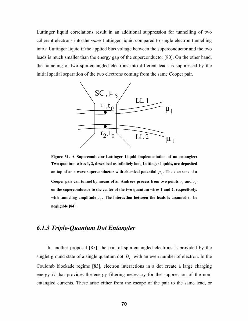
70
Luttinger liquid correlations result in an additional suppression for tunnelling of two
coherent electrons into the same Luttinger liquid compared to single electron tunnelling
into a Luttinger liquid if the applied bias voltage between the superconductor and the two
leads is much smaller than the energy gap of the superconductor [80]. On the other hand,
the tunneling of two spin-entangled electrons into different leads is suppressed by the
initial spatial separation of the two electrons coming from the same Cooper pair.
Figure 31. A Superconductor-Luttinger Liquid implementation of an entangler:
Two quantum wires 1, 2, described as infinitely long Luttinger liquids, are deposited
on top of an s-wave superconductor with chemical potential sµ . The electrons of a
Cooper pair can tunnel by means of an Andreev process from two points 1r and 2r
on the superconductor to the center of the two quantum wires 1 and 2, respectively.
with tunneling amplitude 0t . The interaction between the leads is assumed to be
negligible [84].
6.1.3 Triple-Quantum Dot Entangler
In another proposal [85], the pair of spin-entangled electrons is provided by the
singlet ground state of a single quantum dot CD with an even number of electron. In the
Coulomb blockade regime [83], electron interactions in a dot create a large charging
energy U that provides the energy filtering necessary for the suppression of the non-
entangled currents. These arise either from the escape of the pair to the same lead, or

71
from the transport of a single electron. The idea is to create a resonance for the joint
transport of the two electrons from CD to secondary quantum dots LD and RD , similarly
to the resonance described in Andreev entangler. For this, we need the condition
CRL εεε 2=+ , where Lε and Rε are the energy levels of the available state in LD and
RD , and Cε2 is the total energy of the two electrons in CD . On the other hand, the
transport of a single electron from CD to LD or RD is suppressed by the energy
mismatch RLC U εεε ,≠± , where UC ±ε is the energy of the stnd 1/2 electron in CD .
This can also be explained by two-particle energy conservation [81].
Figure 32. (a) Setup of the triple quantum dot entangler. The central dot
cD can
accept 0, 1 or 2 electrons provided with rate α from the source lead c
l . Its ground
state with 2 electrons is the spin singlet. The electrons can tunnel coherently (with
tunnelling amplitudes 0
T ) between c
D and the two secondary dots L
D and R
D ,
which can only accept 0 or 1 electron and act as energy filters. Each electron from
the singlet pair can finally tunnel out to the drain leads L
l and R
l with a rate γ . (b)
Energy level diagram (single-particle). The dashed arrows represent the single-
electron currents [80].
6.1.4 Coulomb Scattering Entangler
Scanning probe techniques can be applied to a two-dimensional (2D) electron
system formed in a semiconductor heterostructure in order to monitor and control the

72
flow of electrons. In [86], it has proposed to generate spin-entangled pairs of electrons
using this technique to control Coulomb scattering in a interacting 2D electron system. At
a scattering angle of π/2, it is expected that constructive two-particle interference leads to
an enhancement of the spin-singlet scattering probability, while the triplet scattering is
suppressed (see Figure 33). Two quantum point contacts filter electrons from two
reservoirs with initial momenta 21 pp −= . The two detectors (with an aperture angle
δθ2 ) are placed such that only electrons that collide (shaded area) at a scattering angle
around are registered. Because of interference, the scattering amplitude vanishes at 2/π
for the spin-triplet states, allowing only the spin-entangled singlets to be collected: one
electron of the singlet state in detector 1 and its partner in detector 2
Figure 33. (color online). (a) Coulomb scattering entangler (b) Scattering
parameters: P=p1+p2=p’1+p’2 is the total momentum, p=(p1- p2)/2 and p’=(p’1-p’2)/2
are the relative momenta, and θ=<(p, p’) is the scattering angle between them. The
initial (p1; p2 ) and final (p’1; p’2) momenta are connected by a circle of radius p=p’
due to energy and momentum conservation [86].
6.2 Entanglement Detection
The main issue after producing spin entanglement in solid-state structures is how
one can test for the presence of entanglement. In the following, we describe some of the
proposed tests for spin entanglement. Note that it is assumed that an entangler generates

73
pairs of entangled electrons. This investigation is related to some fundamental issues such
as the non-locality of quantum mechanics, especially for massive particles, and genuine
two-particle Aharonov-Bohm effects which are fascinating topics in their own right. The
main idea in all of the following detection schemes is to exploit the unique relation
between the symmetry of the orbital state and the two-electron spin state which makes it
possible to detect an electron spin state via the orbital degrees of freedom.
6.2.1 Coupled Quantum Dots
In [87], it is proposed to measure the transport current and its fluctuations, current
noise, in order to probe the entanglement of two electrons localized in a double-dot. The
double-dot is assumed to be weakly coupled to ingoing and outgoing leads (at chemical
potentials 1µ and 2µ ) with tunneling amplitude T . Also, it is assumed that the dots are
shunted in parallel. In addition to the Coulomb blockade regime [83], the cotunneling
regime [88] is also considered. This means that the charge on the dots is quantized and
because of the energy conservation the single-electron tunneling is forbidden. In this
regime, the current is generated by a coherent virtual process where one electron tunnels
from a dot to one lead and then a second electron tunnels from the other lead to this dot.
The elastic and inelastic cotunneling occur provided that the bias voltage is larger
than the exchange coupling, J>− 21 µµ . Therefore, an electron can either pass through
the upper or lower dot which results in a closed loop by these two paths. A magnetic flux
then gives rise to an Aharonov-Bohm phase h/ABe=ϕ (A is the loop area) between the
upper and the lower paths which results in leading to quantum interference effects. This
transport setting is sensitive to the spin symmetry of the two-electron state on the double
dot. If the two electrons on the double-dot are in the singlet state, then the tunneling
current acquires an additional phase of π leading to a sign reversal of the coherent
contribution compared to that for triplets.

74
6.2.2 Coupled Dots with Superconductor Leads
Another proposal based on double-dots has considered in [89]. In this proposal,
again two quantum dots are shunted in parallel between the leads; however, there is no
direct coupling between them. The two dots are coupled via tunneling (with amplitude
T ) to two superconducting leads. There are two properties which help detecting
entanglement: (1) The s-wave superconductor tends to have an entangled singlet-state on
the dots. (2) The Josephson current through the double dot system provides the detection
mechanism for the spin state.
The spin state (singlet or triplet) on the dot is probed while the superconductor leads
are joined with one additional Josephson junction with coupling J ′ and phase difference
θ . In order to probe the spin state the system is biased with a dc current I until a finite
voltage V appears for CII > , where CI , the spin- and flux-dependent critical current,
will be measured. [81, 89].
6.2.2 Beam Splitter
In order to detect pairwise spin entanglement between electrons, Burkard et al. [90]
proposed to measure a charge current in two mesoscopic wires after transmission through
an electrical beam splitter. In this scheme, the singlet EPR pair enhances the shot noise
power (“bunching”), whereas the triplet EPR pair leads to a suppression of noise
(“antibunching”).
For the detection of spin entanglement of electrons carried by two mesoscopic
wires, a non-equilibrium transport measurement is considered in [90] which is depicted in
Figure 34. An entangler feeds a pair of entangled electrons, one in lead 1 and the other
one in lead 2. The beam-splitter mixes the two current in order to induce scattering
interferences. t and r are the transmission and reflection amplitudes. In this scheme, the
beam splitter ensures that the electrons leaving the entangler have an amplitude t to be
interchanged such that 10 2 << t . The resulting noise is measured in leads 3 and 4. An

75
enhanced noise (bunching) is detected if the entangled provides spin-singlets. On the
contrary, a noise reduction is detected if the entangler provides the entangled spin triplets.
It should be stressed that if bunching (enhancement of shot noise) is detected, it can be
interpreted as a unique signature for entanglement of the injected electrons, since the
maximally entangled singlet is the only state leading to this effect.
Figure 34. Beam-splitter for the detection of entangled electrons. The noise is
measured in leads 3 and 4. An enhanced noise (bunching) is detected if the
entangled provides spin-singlets or, on the contrary, a noise reduction is detected if
the entangler provides the entangled spin triplets [90].
6.3 Bell’s Inequalities
There have been a number of proposals to test Bell’s inequalities with spin-
entangled electrons directly with a spin-sensitive detection scheme in contrast to the
detection scheme in previous section. We do not cover these proposals here. The reader is
referred to [81] and its references.

76
References 1. Nielsen M.A., Chuang I.L.; Quantum Computation and Quantum Information, Cambridge University
Press, UK, 2000. 2. Cirac J.I., Zoller P.; Phys. Rev. Lett., 74, 1995, p. 4091. 3. Turchette Q.A., Hood C.J., Lange W., Mabuchi H., Kimble H.J.; Phys. Rev. Lett., 75, 1995, p. 4710. 4. Jones J.A.; Fortschr. Physik, 48, 2000, p. 909. 5. Vion D., Aassime A., Cottet A., Joyez P., Pothier H., Urbina C., Esteve D., Devoret M.H.; Science,
296, 2002, p. 886. 6. Feynman R.P.; Int. J. Theor. Phys., 21, 1982, p. 467. 7. Feynman R.P.; Foundations of Physics, 16, 1986, p. 507. 8. Deutsch D.; Proc. Royal Soc. London A, 400, 1985, p. 97. 9. Shor P.W.; in: S. Goldwaser, (ed.), Proc. 35th Annual Symposium on Foundations of Computer
Science, IEEE Computer Society, Los Alamos, CA, 1994, p.124. 10. Grover L.K.; in: Proc. 28th Annual ACM Symposium on the Theory of Computing, ACM Press, New
York 1996, p. 212. 11. Wooters W.K., Zurek W.H.; Nature, 299, 802, 1982. 12. Barenco A., Bennett C.H., Cleve R., DiVincenzo D.P., Margolus N., Shor P.,Sleator T., Smolib J.A.,
Weinfurter H.; Phys. Rev. A, 52, 1995, p. 3457. 13. Calderbank A.R., Shor P.W.; Phys. Rev. A, 54, 1996, p. 1098. 14. Ekert A., Jozsa R.; Rev. Mod. Phys., 68, 1996, p. 733. 15. Bugajski S., Klamka J., and Wegrzyn S.; Archiwum Informatyki Teoretycznej i Stosowanej, 13, 2001,
p. 97, ibid., 14, 2002, p. 93. 16. DiVincenzo D P 2000 Fortschr. Phys. 48 771. 17. Hanson R., Witkamp B., Vandersypen L.M.K., Wilems van Beveren L.H., Elzerman J.M., and
Kouwenhoven L.P.; Phys. Rev. Lett., 91, 2003, p. 196802. 18. Barenco A.; Contemp. Phys., 37, 1996, p. 375 19. Jacak L., Hawrylak P., and W´ojs A.; Quantum Dots, Springer-Verlag, Berlin, 1998. 20. Bednarek S., Szafran B., Adamowski J.; Phys. Rev. B, 64, 2001, 195303 21. Adamovski J., Bednarek S., and Szafran B., Schedae Informaticae, V. 14, 2005, pp. 95-111. 22. Tarucha S., Austing D.G., Honda T., van der Hage R.J., Kouwenhoven L.P.; Phys. Rev. Lett., 77,
1996, p. 3613. 23. Kouwenhoven L.P., Oosterkamp T.H., Danoesastro M.W.S., Eto M., Austing D.G., Honda T., Tarucha
S.; Science, 278, 1997, p. 1788. 24. Hanson R., Witkamp B., Vandersypen L.M.K., Wilems van Beveren L.H., Elzerman J.M., and
Kouwenhoven L.P.; Phys. Rev. Lett., 91, 2003, p. 196802 25. Hayashi T., Fujisawa T., Cheong H.D., Jeong Y.H., and Hirayama Y.; Phys. Rev. Lett., 91, 2003, p.
226804. 26. J. M. Elzerman, R. Hanson, L. H. Willems van Beveren, S. Tarucha, L., M. K. Vandersypen and L. P.
Kouwenhoven, Quantum Dots: a Doorway to Nanoscale Physics, Lecture Notes in Physics Vol. 667, W.D. Heiss (ed.), ISBN: 3-540-24236-8, Springer Verlag (Berlin, 2005).
27. V.N. Golovach and D. Loss, Europhys. Lett. 62, 83 (2003). 28. G. Burkard, D. Loss, and D.P. DiVincenzo, Phys. Rev. B 59, 2070 (1999). 29. P. Domokos, J.M. Raimond, M. Brune and S. Haroche, Phys. Rev. A52, 3554 (1995). 30. Cirac J I and Zoller P 1995 Phys. Rev. Lett. 74 4091 31. Gershenfeld N A and Chuang I L 1997 Science 275 350 32. Turchette Q A, Hood C J, Lange W, Mabuchi H and Kimble H J 1995 Phys. Rev. Lett. 75 4710 33. Monroe C, Meekhof D M, King B E, Itano W M and Wineland D J 1995 Phys. Rev. Lett. 75 4714 34. Schmidt-Kaler F, H¨affner H, Riebe M, Gulde S, Lancaster G P T, Deuschle T, Becher C, Roos C F,
Eschner J and Blatt R 2003 Nature 422 408 35. Shor P W 1994 Proc. 35th Symposium on the Foundations of Computer Science (IEEE Computer
Society Press) p 124
77
36. Vandersypen L M K, Steffen M, Breyta G, Yannoni C S, Sherwood M H and Chuang I L 2001 Nature 414 883
37. Loss D and DiVincenzo D P 1998 Phys. Rev. A 57 120 38. V N Golovach and D Loss., Semiconductor Science and Technology, 17:355–366, March 2002. 39. Veronica Cerletti, W A Coish, Oliver Gywat and Daniel Loss 2005 Nanotechnology 16 R27-R49 40. Vitaly N. Golovach, Daniel Loss, Semicond. Sci. Technol. 17, 355- 366 (2002); cond-mat/0201437. 41. Guido Burkard, Hans-Andreas Engel, and Daniel Loss, Fortschritte der Physik 48, 965 (2000) (special
issue on Experimental Proposals for Quantum Computation), eds. H.-K. Lo and S. Braunstein; see cond-mat/0004182.
42. A. Barenco et al., Phys. Rev. A 52, 3457 (1995). 43. Meier F, Levy J and Loss D 2003 Phys. Rev. Lett. 90 047901 44. Levy J 2001 Phys. Rev. A 64 052306 45. D. Bacon, J. Kempe, D. A. Lidar, and K. B. Whaley, Phys. Rev. Lett. 85, 1758–1761 (2000) 46. DiVincenzo, D.P.; Bacon, D.; Kempe, J.; Burkard, G.; Whaley, K.B, Nature (16 Nov. 2000), vol.408,
no.6810, pp. 339-342 47. Friesen M, Rugheimer P, Savage D E, Lagally M G, van der Weide D W, Joynt R and Eriksson M A
2003 Phys. Rev. B 67 121301(R) 48. B.E. Kane, Nature (London) 393, 133 (1998). 49. Stoneham A M, Fisher A J and Greenland P T 2003 J. Phys.: Condens. Matter 15 L447 50. Imamoglu A, Awschalom D D, Burkard G, DiVincenzo D P, Loss D, Sherwin M and Small A 1999
Phys. Rev. Lett. 83 4204 51. A Skinner, M Davenport, and B Kane., Phys. Rev. Lett., 2003 (90), 087901. 52. B. El-kareh, Fundamentals of Semiconductor Processing Technology, Boston: Kluwer, 1995. 53. J. D. Plummer, M. D. Deal, P. B. Griffin, Silicon VLSI Technology, New Jersey: Prentice Hall, 2000. 54. D. K. Schroder, Semiconductor material and device characterization, New York: Wiley, 1990. 55. L.L. Sohn, L.P. Kouwenhoven, G. Schön, proceedings of the Advanced Study Institute on Mesoscopic
Electron Transport, 1997. 56. V D Wiel W G, De Franceschi S, Elzerman J M, Fujisawa T, Tarucha S and Kouwenhoven, LP 2003
Rev. Mod. Phys. 75 1. 57. Bonadeo N H, Erland J, Gammon D, Park D, Katzer, 1998 Science 282 1473. 58. Kodera T, van der Wiel W G, Ono K, Sasaki S, Fujisawa T and Tarucha, 2004 Physica E 22518. 59. Leonard D, Krishnamurthy M, Reaves C M, Denbaars S P and Petroff P M, 1993 Appl. Phys. Lett. 63
3203. 60. Eberl K, Lipinski M O, Manz Y M, Winter W, Jin-Phillipp N Y and Schmidt O G, 2001 Physica E 9
164. 61. Lee H, Johnson J A, Speck J S and Petroff P M, 2000 J. Vac. Sci. Technol. B 18 2193. 62. Schedelbeck G, Wegscheider W, Bichler M and Abstreiter G, 1997 Science 278 1792. 63. Alivisatos A P, 1996 Science 271 933. 64. Ouyang M and Awschalom D D, 2003 Science 301 1074. 65. R. Blatt and P. Zoller, Eur. J. Phys. 9, 250-279 (1988). 66. H.J. Mamin, R. Budakian, B.W. Chui, and D. Rugar, Phys. Rev. Lett. 91, 207604 (2003). 67. D. Rugar, R. Budakian, H. J. Mamin & B. W. Chui, Nature, Vol 430, 15 JULY 2004. 68. M. Xiao, I. Martin, E. Yablonovitch, and H. W. Jiang, Nature, Vol 430, 22 JULY 2004. 69. M. Ciorga, A.S. Sachrajda, P. Hawrylak, C. Gould, P. Zawadzki, Y. Feng, Z. Wasilewski, Physica E
11 (2001) 35– 40 70. D. Sprinzak, Y. Ji, M. Heiblum, D. Mahalu, and H. Shtrikman, Phys. Rev. Lett. 88, 176805 (2002). 71. J. M. Elzerman, R. Hanson, L. H. Willems van Beveren, B. Witkamp, L. M. K. Vandersypen & L. P.
Kouwenhoven, Nature, Vol 430, 22 JULY 2004. 72. DiVincenzo D P and Loss D 2005 Phys. Rev. B 71, 035318 73. D.Loss, D.P.Di Vincenzo 2003 preprint cond-mat/0304118 74. G.Burkard, D.Loss 2002 Phys. Rev. Lett. 88 047903 75. L.S.Levitov and E.I. Rashba 2003 Phys. Rev. B 67 115324 76. Glavin B A and Kim K W 2003 Phys. Rev. B 68 045308 77. Cheng J L, Wu M W and L¨u C 2004 Phys. Rev. B 69 115318 78. Merkulov I A, Efros Al L and Rosen M 2002 Phys. Rev. B 65 205309. 79. C.H. Bennett and D.P. DiVincenzo, Nature, 404, (2000), 247.
78
80. DS Saraga, G. Burkard, JC Egues, H.-A. Engel, P. Recher, D. Loss Turk. J. Phys. 27, 427 (2003). 81. Guido Burkard, Review article prepared for Handbook of Theoretical and Computational
Nanotechnology, cond-mat/0409626. 82. Recher, P., E. V. Sukhorukov, and D. Loss, 2001, Phys. Rev. B 63, 165314. 83. L.P. Kouwenhoven, G. Schön, and L.L. Sohn in 'Mesoscopic Electron Transport' NATO ASI Series E
- Vol. 345, pp. 1-44, Kluwer (1997). 84. Recher, P., and D. Loss, 2002, Journal of Superconductivity and Novel Magnetism 15, 49, cond-
mat/0202102. 85. Saraga, D. S., and D. Loss, 2003, Phys. Rev. Lett. 90, 166803. 86. Saraga, D. S., B. L. Altshuler, D. Loss, and R. M. Westervelt, 2004, Phys. Rev. Lett. 92, 246803. 87. D., and D. P. DiVincenzo, 1998, Phys. Rev. A 57(1), 120. 88. Averin, D. V., and Y. V. Nazarov, 1992 (Plenum Press, New York), volume 294 of NATO ASI Series
B: Physics. 89. Choi, M.-S., C. Bruder, and D. Loss, 2000, Phys. Rev. B 62, 13569 90. Burkard, G., D. Loss, and E. V. Sukhorukov, 2000b, Phys. Rev. B 61, R16303, cond-mat/9906071.