Quantum Cellular AutomataO
22
AD-A283 351 Annual Report for the Period 1 July 1993 - 30 June 1994 Quantum Cellular AutomataO Wolfgang Porod, Craig S. Lent, and Gary H. Bernstein Department of Electrical Engineering University of Notre Dame Notre Dame, IN 46556 94- 25767 Accesion For NTIS CRA&M DTIC TAB Unannounced Justificatio n. Submitted By ................................................ to the Distribution I Office of Naval Research Availability Codes Avail a;.d for 800 North Quincy Street Dist Special Arlington, VA 22217 Grant No: N00014-93-1-1084 R&T Project: cd14027 --- 02 94 8 15 0.10 i IU VaIc
Transcript of Quantum Cellular AutomataO

AD-A283 351Annual Reportfor the Period
1 July 1993 - 30 June 1994
Quantum Cellular AutomataO
Wolfgang Porod, Craig S. Lent, and Gary H. Bernstein
Department of Electrical EngineeringUniversity of Notre Dame
Notre Dame, IN 46556
94- 25767 Accesion For
NTIS CRA&MDTIC TABUnannouncedJustificatio n.
Subm itted By ................................................to the Distribution I
Office of Naval Research Availability CodesAvail a;.d for
800 North Quincy Street Dist Special
Arlington, VA 22217
Grant No: N00014-93-1-1084R&T Project: cd14027 --- 02 94 8 15 0.10
i IU
VaIc

Quantum Cellular Automata Porod, Lent, and Bernstein
Research Summary
The Notre Dame group has developed a new paradigm for ultra-dense and ultra-fast informationprocessing in nanoelectronic systems. These "Quantum Cellular Automata" (QCA's) are the firstconcrete proposal for a technology based on arrays of coupled quantum dots. The basic buildingblock of these cellular arrays is the Notre Dame Logic Cell, as it has been called in the literature.The phenomenon of Coulomb exclusion, which is a synergistic interplay of quantum confinementand Coulomb interaction, leads to a bistable behavior of each cell which makes possible their usein large-scale cellular arrays. The physical interaction between neighboring cells has beenexploited to implement logic functions. New functionality may be achieved in this fashion, andthe Notre Dame group invented a versatile majority logic gate. In a series of papers, the feasibilityof QCA wires, wire crossings, inverters, and Boolean logic gates was demonstrated. A major find-ing is that all logic functions may be integrated in a hierarchical fashion which allows the designof complicated QCA structures. The most complicated system which was simulated to date is aone-bit full adder consisting of some 200 cells. In addition to exploring these new concepts,efforts are under way to physically realize such structures both in semiconductor and metal sys-tems. Extensive modelling work of semiconductor quantum dot structures has helped identifyoptimum design parameters for QCA experimental implementations. In the first year of thisproject, the experimental effort has laid the ground work for the study of Coulomb coupling inquantum dot structures. The newly acquired ultra-high resolution field emission scanning electronmicroscope was installed and used to examine nanostructures with a resolution of 1 nanometer.Coupled dot structures were fabricated in Gallium Arsenide heterostructures and await testing inthe newly-established cryogenic measurement facility
Organization of the Report
Research D escription ............................................................................................. 3Publications and Presentations ............................................................................ 10
List of Journal Publications ................................................................. 10
List of Conference Publications and Presentations ............................... 11
List of Invited Seminars ....................................................................... 12
List of Honors, Awards, and Appointments .......................................... 13
Appendix: Coverpages of Reprints ..................................................................... 14
Annual Report, July '93 - June '94 2

Quantum Cellular Automata Porod, Lent, and Bernstein
Research Description
* Bistability of Coulomb-coupled quantum dot cell. For a family of cell designs, based on"quantum dot molecules" composed of near-by quantum dots, we demonstrated that Coulombinteraction produces a very nonlinear bistability in the charge distribution of the cell. The cellground state is in one of two states depending on the electrostatic environment, which is in turndetermined by neighboring cells. We introduced the concept of cell polarization to describe thepossible alignment of charge within the cell.
* QCA binary wires. The intrinsic bistability of each cell coupled with the Coulomb interactionbetween cells causes a linear array of cells to align in the same polarization. The linear array thusacts as a binary wire, transmitting information from the driven end to the unconstrained end. Wehave explored the behavior of the wire for the entire parameter space of our model Hamiltonian.We found that the wire functioned well so long as the energetics of the Coulomb interactiondominated the kinetic energy which tends to cause the two-electron wavefunction to spread. Thebistability of each cell in the wire also resulted in an insensitivity to geometrical variations andother parameter fluctuations from cell to cell.* QCA majority logic gate. We designed the basic logical device in this architecture - themajority logic gate. Signals from three input wires converge on a single cell, from which the outputemerges. The majority logic gate itself contains only two electrons and performs a logical functionthat would take many transistors to accomplish.
• QCA inverter and wire crossing. We devised a scheme for crossing two QCA wires in theplane by exploiting the symmetry of the charge distribution in the cells. This allows design of morecomplicated logical devices without the need to construct bridges for one QCA wire to crossanother. A simple binary logical inverter device was also devised.
* Hierarchical design of QCA circuits: the full adder. We designed and simulated a single-bitfull adder using QCA cells. The calculation involved self-consistently solving the Schr6dingerequation for over 200 electrons. The Coulomb interaction between each pair of electrons wasincluded. The results showed that the adder worked correctly for all possible inputs, and thathierarchical design rules are possible. Having developed the basic logical primitives, wires,inverters, majority gates, and wire crossings, design and layout can proceed without concern aboutspurious Coulomb interactions between various parts of the system. This is fundamentally due tothe fact the cell has only a quadrupole moment with a rapidly decaying field strength.
* QCA bistability implemented in metallic system. The QCA systems we have considered sofar were envisioned as being implemented in semiconductor quantum dots in which the totalnumber of electrons could be made small and be well controlled. We have extended andgeneralized these ideas to cells composed of small metallic tunnel-junctions. In this case, each cellcontains two extra electrons and the coupling between cells is capacitive (and therefore morecontrollable).
• Time dependence of QCA devices. By design, the exact time evolution of the QCA deviceafter the inputs are switched is not crucial. The architecture works by mapping the ground state ofthe system, subject to the (newly imposed) boundary conditions, onto the solution of the logical orarithmetic problem. The details of how the system reaches that ground state, dissipating theswitching energy, are not important. An exception to this occurs if the system dynamics are such
Annual Report, July "93 - June '94 3

Quantum Cellular Automata Porod, Lenm, and Bernsein
that the system becomes stuck in a metastable state and is unable to reach the new ground state ina reasonable time. In particular, this may occur in the situation of wire fan-out, where one signal isbeing spread to several different devices. To address this issue we have begun time-dependentcalculations of the switching behavior of QCA devices. While preliminary results are encouraging,we have not completed this stage of our investigation.
* Boundary Conditions for Quantum Devices with Exposed Surfaces. We have developed anumerical technique for the simulation of the electrostatic potential and the electronic states inquantum device structures. Since we are particularly interested in quantum dots in the few electronregime, one of the main design strategies is to utilize semiconductor heterostructures with veryshallow two-dimensional electron gases. Metallic gates on the semiconductor surface will thenresult in crisp confining potential landscapes. Since the electrons now are close to the surface, anysurface charges will tend to alter the confining potentials. This poses challenges for the modellingof these structures since no simple boundary conditions for the potential on the surface areapplicable. The usual Dirichlet and von Neumann boundary conditions, which are routinelyemployed for larger structures, are too simplistic in this case. In our modelling, therefore, weinclude both the semiconductor domain and the adjacent region of the dielectric (air or vacuum).The usual boundary conditions on the semiconductor surface are then replaced by matchingconditions for the electrostatic potential and the dielectric flux. Any surface charges, such as theones due to charged surface states, will lead to a discontinuity of the dielectric flux. We havedeveloped an efficient numerical technique to solve for the electrostatic potential in the combinedsemiconductor - dielectric domains. Our approach is based on a coupled finite element method forthe semiconductor domain and a boundary element method for the dielectric domain. Thecombined linear system of equations which has to be solved is only slightly larger than the one forthe semiconductor alone.
* Modelling of Quantum Dots in the Few Electron Regime. Utilizing our numerical techniquefor the simulation of quantum device structures, we have studied field-confined quantum dots inthe few electron regime. This numerical modelling will yield the design parameters for theexperimental realization of QCA quantum dots cells. So far, we have explored the feasibility ofseveral top-gate configurations and we have studied their capability of producing crisp confiningpotentials. The usual mode is to employ top gates with a negative bias, which repel the carriers inthe two-dimensional electron gas underneath. Quantum wires and quantum dots are realized in theareas below metal-free regions on the surface, which expose the semiconductor to the ambientdielectric. Our modelling shows that for typical dimensions and structural parameters, it will bevery difficult to use negative gate biases to tune quantum dots which are occupied by a smallnumber of electrons. Even for extremely small separations of the 2DEG from the surface, say 40nm or so, the confining electrostatic potential is still quite gradual. It will also be very difficult torealize top metal gates with openings which are on the order of only a few tens of nanometers. Inaddition, the geometrical features of the metal opening are several times larger than the induceddot underneath. This will make it very hard, if not impossible, to fabricate a QCA cell, whichcontains several closely-spaced dots, by utilizing negative top-gate biasing. An alternate approachis to use positive top-gate biasing. In this scheme, one starts out with a structu"- which does notpossess a two-dimensional electron gas without biasing. A positive bias applied to the metal on thetop surface may then induce electrons underneath. Our modelling of this accumulation modeshows that geometrical considerations allow the realization of closely-spaced dots. However, thepositive bias required is so large that the structure becomes leaky (between top metal and 2DEG).
Annual Report, July '93 - June '94 4

Quatum Cellular Automata Porod, Lent, and Bernstein
The most promising approach, which we were able to identify based on our modelling work, is acombined depletion mode (negative top-gate bias) and accumulation mode (positive top-gate bias).We envision a top-gate geometry which consists of a rather large opening (negative bias) in whichseveral metal dots (positive bias) are placed. The negative gate just barely depletes the 2DEG, andthe carriers may be brought back with a rather small positive bias. We are hopeful that a QCA cellmay be realized by this combined biasing approach. The opening in the negative gate will definea whole cell and the dots in each cell will be induced by separate positively-biased gates placedinside the opening. The modelling of experimental test structures is under way.
* QCA Realization in rn-V's. Graduate student Greg BazAn has made significant progress overthe last year toward demonstration of Coulomb coupling in III-V material. He has designed a setof molecular beam epitaxy layers provided by Dr. J. Furdyna at Notre Dame, improved theoperation of the Heliox cryostat dewar, and fabricated first devices to be tested soon. Figure 1shows SEM micrographs of a set of two "dots" fabricated on a 2DEG designed to detect thepresence of one electron per dot. The two quantum dots are at the top and bottom of the centerbounded at the top by TD, F, QG, and R, and at the bottom by JN, P, QG, and H. In theconfiguration shown, a wide barrier has been built between the quantum dots so that the dots canbe tested independently. In future iterations, this barrier will be made thinner or replaced by a splitgate so that the effects of coupling can be investigated.
By biasing these Schottky contacts correctly, the dot areas can be squeezed so that the energy wellof the dot can support a varying electron population. We will first discuss the top quantum dot.Electrons are brought into, or pushed off of, the dot through split-gates R-TD and F-TD by ohmiccontacts SE. The presence of extra electronic charge on the dot is detected through biasing splitgate B-TD below the first conductance step. The conductance there is small, due only to thermalbroadening of the Fermi level, but will be noticeably modified by the presence a single extra elec-tron. Therefore, we see that the structure consists of two dots and two detectors. By the presenceof a backgating layer structure, we can independently change the electron population and the dotsize, while biasing split gates to place or remove single electrons from a dot and observing theeffect on the adjacent dot through its detector. This is a very complicated experiment, andalthough much has been accomplished so far, significant groundwork is still required before wecan test the entire functionality of the structure.
* QCA Realization in Metals. The identical functionality as that described above can beperformed in an entirely metal/insulator system using single electron charging phenomena.Graduate Student Xiaokang Huang has undertaken to demonstrate Coulomb coupling using tunneljunctions fabricated by the technique of shadow evaporation1 pioneered by Dolan.
Lafarge et al.2 have shown that it is possible to detect, by capacitive coupling only, a single elec-tron tunneling onto a metal island. Using shadow evaporation technology, we have designed afour-dot QCA cell, as suggested by C. Lent and shown in Fig. 2. Cl and similar structures repre-
1. G. J. Dolan, Phys. Rev. Lett. 31, 109 (1977).2. P. Lafarge, H. Pothier, E. R. Williams, D. Esteve, C. Urbina, and M. H. Bevoret, Phys. B- Condensed
Matter $5, 327 (1991).
Annual Report, July '93 - June '94 5

Quantum Cellular Automnat Pored, LeAnt, and Bemszein
sent tunnel junctions with all metal adjacent to "a" representing a "dot" capacitively coupled
T A B C DS E
R F
Q G
P H
0 N M L K J
Figure 1. Electron micrograph of devices fabricated by EBL for the purpose of testing Coulombcoupling between quantum dots. All metal in this photo are Schottky layers for the creationof energy barriers in the 2DEG.
(through capacitor Cc) to the metal at "c", another quantum dot.
Figure 3 shows a plot of the physical layout of the complete cell. All structures are metal, exceptfor thin AlOx layers acting as tunnel barriers at the overlapping points, indicated by the shadedregions. As single electrons tunnel onto a metal island, e.g. at I1, adjacent metal lines at I1capacitively couple the electric field to 13 and affect the ability for an electron to tunnel onto 13.Electrodes 2,4,7, and 9 can be used to bias the dots, and electrodes 3 and 8 will be used to screenthe bias fields from each other.
Figure 4 shows a cross-section of a thin layer of PMMA over a thick layer of PMMA/MAAcopolymer which, after EBL exposure and developing, has resulted in an extreme undercut profileallowing evaporation of metal at relatively large angles- as much as 6 degrees off vertical. At thetop,the thin opening is a faithful representation of the EBL exposure in PMMA, whereas thePMMA/MAA developed more quickly creating the undercut. Visible is the aluminum line evap-orated through the slit at the top and resting on the surface of the wafer off from the vertical. This
Annual Report, July '93 - June '94 6

Qmnum Cellular Automata Porod, Lent, and Bernstein
technique allows us to evaporate a line, oxidize it in situ, and then, after tilting the sample, evapo-rate another line perpendicular to it so that an overlap is achieved resulting in a single electrontunnel junction. Figure 5 shows perpendicular aluminum lines overlapping in a region approxi-mately 50 by 80 nm 2. So far, complete structures have been fabricated, but accurate control oftunneling resistance has not been achieved.
Cl C3
Cs C¢ C s
CT
(a) Cs bcc Cs
C2 I 4
a c
(b)b d0 ----------------.- 0
Figure 2. (a) Schematic of the prototype QCA consisting of 4 single electron "dots." (b) Diagram of the QCAcell formed by (a).
Annual Report, July '93 - June '94 7

Quantum Cellular Automata Porod, Lent, and Bernstein
K - 10
CI
C3
133 CTI
CDLII 8
C2 14
C4
56
Figure 3. Physical layout of the prototype QCA shown in Fig. 5.
Figure 4. FESEM micrograph of cross-sectioned double resist layers used for shadow evaporation. The metal lineevaporated at 6 degrees off normal is visible on the surface of the wafer.
Annual Report, July '93 - June '94 8

QuM Cellular Autmata Porod, LeUm, and Besmein
Figure 5. FESEM micrograph of tunnel junction formed by the Dolan bridge technique. A second, unused, verticalline exists due to the double, angled shadow evaporation. The aluminum has been oxidized between evapora-tions.
Annual Report, July '93 - June '94 9

Quantum Cellular Autommaa Porod, Lent, and Bernstein
Journal Publications
Craig S. Lent, P. Douglas Tougaw, Wolfgang Porod, and Gary H. Bernstein, "Quantum CellularAutomata," Nanotechnology 4, 49-57 (1993).
Craig S. Lent, P. Douglas Tougaw, and Wolfgang Porod, "Bistable Saturation in Coupled Quan-tum Dots for Quantum Cellular Automata," Applied Physics Leners 62, 714 (1993).
X. Huang, G. Bazdn, G. H. Bernstein, "New Technique for Computation and Challenges for Elec-tron Beam Lithography," Journal of Vacuum Science and Technology B, 11(6), 2565-2569(1993).
Craig S. Lent and P. Douglas Tougaw, "Lines of interacting quantum-dot cells: a binary wire,"Journal of Applied Physics, 74, 6227 (1993).
R Douglas Tougaw, Craig S. Lent, and Wolfgang Porod, "Bistable saturation in coupled quantum-dot cells," Journal of Applied Physics 74, 3558-3566 (1993).
Craig S. Lent and P. Douglas Tougaw, "Bistable saturation due to single electron charging in ringsof tunnel junctions," Journal of Applied Physics 75, 4077-4080 (1994).
P. Douglas Tougaw and Craig S. Lent, "Logical devices implemented using quantum cellularautomata," Journal of Applied Physics 75, 1818-1825 (1994).
Minhan Chen, Wolfgang Pored, and David J. Kirkner, "A Coupled Finite Element/Boundary Ele-ment Method for Semiconductor Quantum Devices with Exposed Surfaces," Journal ofApplied Physics 75, 2545-2554 (1994).
Annual Report July '93 - June '94 10

Quantum Cellular Automata Porod, Lent, and Bemstein
Conference Publications and Presentations
Gary H. Bernstein, Xiaokang Huang, Greg Bazln, Davide A. Hill, Craig S. Lent, and WolfgangPorod, "New Technique for Computation and Challenges for Electron Beam Lithography,"poster presented at the Three-Beams Conference, San Diego, California, June 1993,
Craig S. Lent, Wolfgang Porod, and P. Douglas Tougaw, (Invited), "Quantum Simulation of Sev-eral-Particle Systems," presented at the Workshop on Combined Self-Consistent ParticleTransport Simulation and Full Wave Dynamic Field Simulation for Monolithic Solid StateDevice and Circuit Calculations of the IEEE Microwave Theory and Techniques Symposium,Atlanta, Georgia, June 1993.
Minhan Chen, Wolfgang Porod, and David J. Kirkner, "Boundary Conditions for QuantumDevices with Exposed Surfaces," Proceedings of the International Workshop on Computa-tional Electronics, C. Snowden and M. Howes, eds., pp. 255 - 259; presented at the Interna-tional Workshop on Computational Electronics, Leeds, England, August 1993.
Craig S. Lent, Wolfgang Porod, and P. Douglas Tougaw, "Quantum Simulation of Several-Parti-cle Systems," Proceedings of the "International Workshop on Computational Electronics, C.Snowden and M. Howes, eds., pp. 303 - 307; presented at the International Workshop onComputational Electronics, Leeds, England, August 1993.
C. S. Lent, P. D. Tougaw, W. Porod, and G. H. Bernstein, (Invited), "Quantum Cellular Autom-ata," presented at the Midwest Solid State Theory Symposium, Detroit, Michigan, October,1993.
Craig S. Lent, Wolfgang Porod, and Gary H. Bernstein, (Invited), "Quantum Cellular Automata,"presented at the 1993 ARPA ULTRA review meeting, Santa Fe, New Mexico, October 1993.
Craig S. Lent, (Invited), "Quantum Cellular Automata," International Conference on AdvancedMicroelectronic Devices and Processing, Sendai, Japan, March 1994.
Craig S. Lent, P Douglas Tougaw, and Wolfgang Porod, "Quantum Cellular Automata," abstractpublished in the Bulletin of the APS, Vol. 39, No. 1, p. 799, March 1994; presented at the 1994March Meeting of the American Physical Society, Pittsburgh, Pennsylvania, March 1994.
P. Douglas Tougaw and Craig S. Lent, "Dynamics of a linear array of coupled quantum-dot cells,"American Physical Society March Meeting, Pittsburgh, Pennsylvania, 1994.
Minhan Chen and Wolfgang Porod, "Numerical simulation of electron confinement in quantumdot structures," abstract published in the Bulletin of the APS, Vol. 39, No. 1, pp. 800 - 801,March 1994; presented at the 1994 March Meeting of the American Physical Society, Pitts-burgh, Pennsylvania, March 1994.
B. Campbell, G. H. Bernstein X. Huang, and G. BazAn, "A Novel Method for Producing Nano-structures in Silicon Inversion Layers," presented at the March Meeting of the American Phys-ical Society, Pittsburgh, Pennsylvania, March 1994.
G. BazAn and G. H. Bernstein, "Nanolithography over Very Large Scan Fields," poster presentedat Great Lakes Symposium on VLSI, Notre Dame, Indiana, March, 1994.
X. Huang, G. Baz7n, and G. H. Bernstein, "Proximity Effects in Ultradense Patterns Exposed byElectron Beam Lithography," poster presented at Great Lakes Symposium on VLSI, Notre
Annual Report, July '93 - June '94 11

Quantum Cellular Automata Porod, Lent, and Bemstein
Dame, Indiana, March, 1994.
Craig S. Lent, (Invited), "Quantum Cellular Automata," presented at the Engineering FoundationConference on Surfaces and Interfaces in Mesoscopic Devices, Kona, Hawaii, April 1994
Minhan Chen and Wolfgang i- -,Lod, "Numerical simulation of electron confinement in quantumdot structures," presented at the Engineering Foundation Conference on Surfaces and Inter-faces in Mesoscopic Devices, Kona, Hawaii, April 1994.
Craig S. Lent, Manhua Leng, and P. Douglas Tougaw, (Invited), "Quantum Device Modeling,"presented at the Third International Workshop on Computational Electronics, Portland, Ore-gon, May 1994.
P. Douglas Tougaw and Craig S. Lent, "Dynamic Behavior of Coupled Quantum Dot Cells," pre-sented at the Third International Workshop on Computational Electronics, Portland, Oregon,May 1994.
Minhan Chen and Wolfgang Porod, "Numerical Simulation of the Effect of Surface Charges onElectron Confinement in Quantum Dot Structures," presented at the Third International Work-shop on Computational Electronics, Portland, Oregon, May 1994.
Invited Seminars
"Quantum Cellular Automata," Craig S. Lent, seminar presented at Wright Laboratories, Wright-Patterson AFB, Dayton Ohio, September 1993.
"Quantum Cellular Automata," Craig S. Lent, seminar presented at the Department of ElectricalEngineering, University of Maryland, College Park, Maryland, October 1993.
"Quantum Dots Coupled in a Cellular Automata Architecture," Craig S. Lent, seminar presentedat the Department of Physics and Astronomy, Michigan State University, East Lansing, Mich-iga'n, January 1994.
"Quantum Cellular Automata," Wolfgang Porod, seminar presented at Sandia National Laborato-ries, Albuquerque, New Mexico, February 1994.
"Quantum Cellular Automata," Craig S. Lent, colloquium presented at Indiana University-PurdueUniversity, Indianapolis, April, 1994.
"Quantum Device Fabrication at Notre Dame," Gary H. Bernstein, seminar presented at Motor-ola, Inc., Tempe, Arizona, June 1994.
Annual Report, July '93 - June '94 12

Quantum Cellular AutM=a= Porod, Lent, and Bernswin
Honors, Awards, and Appointments
Wolfgang Porod served on the Advisory Committee of the Second International Workshop onComputational Electronics, Leeds, England, August 1993.
Wolfgang Porod was a member of the Technical Program Committee of the Conference on NeuralNetworks and Artificial Intelligence of the SPIE International Symposium on Substance Iden-tification Technologies, Innsbruck, Austria, 4 - 8 October 1993.
Wolfgang Porod was a member of the Review Team for the Electrical and Computer EngineeringGraduate Program Review, The University of New Mexico, Albuquerque, February 1994.
Gary H. Bernstein was a Session Chair at the March Meeting of the American Physical Society,Pittsburgh, Pennsylvania, March 1994.
Wolfgang Porod was a member of the Technical Program Committee of the Third InternationalWorkshop on Computational Electronics, Portland, Oregon, May 1994.
Gary H. Bernstein was a member of the Technical Program Committee and Session Chair at The38th International Symposium on Electron, Ion and Photon Beams, New Orleans, Louisiana,May 1994.
Annual Report, July '93 - June '94 13

Quantum Cellular Automata Porod, Lent, and Bernstein
APPENDIX: Coverpages of Reprints
Annual Report, July '93 - June 494 14

o . Nanotechnology 4 (1993) 49-57. Printed in the UK
Quantum cellular automata
Craig S Lent, P Douglas Tougaw, Wolfgang Porod andGary H BernsteinDepartment of Electrical Engineering, University of Notre Dame, Notre Dame, IN46556, USA
Received 1 August 1992, accepted for publication 24 December 1992
Abstract. We formulate a new paradigm for computing with cellular automata(cAs) composed of arrays of quantum devices-quantum cellular automata.Computing in such a paradigm is edge driven. Input, output, and power aredelivered at the edge of the CA array only; no direct flow of information or energyto internal cells is required. Computing in this paradigm is also computing withthe ground state. The architecture is so designed that the ground-stateconfiguration of the array, subject to boundary conditions determined by theinput, yields the computational result. We propose a specific realization of theseideas using two-electron cells composed of quantum dots, which is within thereach of current fabrication technology. The charge density in the cell is veryhighly polarized (aligned) along one of the two cell axes, suggestive of a two-state CA. The polarization of one cell induces a polarization in a neighboring cellthrough the Coulomb interaction in a very non-linear fashion. Quantum cellularautomata can perform useful computing. We show that AND gates, OR gates,and inverters can be constructed and interconnected.
1. Introduction quantum devices-thus, quantum cellular automata(QCA). A QCA would consist of an array of quantum
The continual down-scaling of device dimensions in device cells in a locally-interconnected architecture. Themicroelectronics technology has led to faster devices and cell state becomes identified with the quantum state ofdenser circuit arrays with obvious benefits to chip perfor- the mesoscopic device. Two-state CAs are attractivemance. Dramatic as they have been, these changes have because they naturally admit to encoding binary in-been evolutionary in nature in that even the most formation. For a two-state QCA, each cell should haveadvanced chips use the same paradigms for computing as two stable quantum states. The state of a given celltheir more primitive ancestors. There is now much should influence the state of the neighboring cells. Twoexpectation that the availability of very dense device ingredients are essential then: (1) the bistability of the cell,arrays might lead to new paradigms for information and (2) coupling to neighboring cells.processing based on locally-interconnected architectures We propose a cell which is composed of coupledsuch as cellular automata (CA) and cellular neural net- quantum dots occupied by two electrons [7]. The re-works [1]. quisite bistability is accomplished through the inter-
There has also been considerable interest in quantum action of quantum confinement effects, the Coulombmesoscopic structures for their possible application as interaction between the two electrons, and the quantiza-devices [2]. Much has been learned about the behavior of tion of charge [8]. The intercellular interaction is pro-electrons flowing through very small structures in semi- vided by the Coulomb repulsion between electrons inconductors. Various investigators have pointed out the different cells. We analyze this cell and the interactionsnatural link between mesoscopic quantum systems and between neighboring cells in section 2.cellular automata architectures [3-5]. Because quantum In section 3 we propose a new paradigm for howstructures are necessarily so small, it is difficult to computation could be performed with an array ofconceive of a regime in which a single quantum device quantum devices. Because no direct connections can becould drive many other devices in subsequent stages [6]. made to interior cells, information or energy can enter theFurthermore, the capacitance of ultra-small wires form- array only from the edges. Edge-driven computationing the connections to each device would tend to imposes further constraints on the nature of the comput-dominate the behavior of an assembly of quantum ing process [9]. The lack of direct connections to thedevices. For these reasons locally interconnected interior cells also means that no mechanism exists forstructures such as cellular neural networks and CAs may keeping the array away from its equilibrium ground-stateprovide the natural architecture for quantum devices, configuration. We are therefore led to use the ground
We focus here on the idea of employing CA archi- state of the array to do the computation. Computing withtectures which are compatible with nanometer-scale the ground state means that the physics of the array must
0957-4484/93/010049+09 S07.50 © 1993 lOP Publishing Ltd 49

Bistable saturation in coupled quantum dots for quantum cellular automataCraig S. Lent, P. Douglas Tougaw, and Wolfgang PorodDepartment of Electrical Engineering Unwversurv of Notre Dame. Notre Dame. Indiana 46556
(Received 5 May 1992: accepted for publication 23 November 1992)
A simple model quantum dot cell containing two electrons is analyzed as a candidate forquantum cellular automata implementations. The cell has eigenstates whose charge density isstrongly aligned along one of two directions. In the presence of the electrostatic perturbation dueto a neighboring cell, the ground state is nearly completely aligned (polarized) in one directiononly. The polarization is a highly nonlinear function of the perturbing electrostatic fields andshows the strong bistable saturation important for cellular automation function.
Nanoscale quantum structures with potential deviceapplications have been an active area of exploration for ffol Eoni.,+ I t,.j(aXa .,oa,.a)several years. A frequent criticism' of many of these struc- La "j'a
tures is the absence of the saturating behavior which forces + E (1)conventional transistor elements into one of two stable > ,+Vn.'
states, "on" or "off." Such bistable saturation is importantto keep device performance robust in the presence of phys- where the number operator n,.,=a,.oa,., and the operatorical inhomogeneities and noise.- a 0.t creates an electron at site i with spin a. The cell pa-
The possibility of realizing cellular automata (CA) rameters which define the Hamiltonian are then the on-sitewith regular arrays of quantum dots has been suggested by energy, E0 , the tunneling energies. t,.,, and the on-site Cou-Bate and others. 3 In one example, the necessary nonlinear lomb charging energy, EQ. The parameter VQ is deter-response of each dot is the result of resonant tunneling mined by fundamental constants and the dielectric con-through the dot. We focus on a different paradigm in stant of the material in which the dots are formed. A fixedwhich each cell of the CA is composed of groups of cou- positive charge ý is assumed at each site sufficient to main-pled quantum dots. The confining potentials are such that tain overall cell charge neutrality. For an isolated cell, thiselectrons can tunnel between dots in the same cell but not only renormalizes E0, but it is important in calculating thebetween different cells. Quantum mechanics and the Cou- interaction between cells as is done below.
lomb interaction in each cell determine the possible cell For the numerical results we discuss here we choose
states. The Coulomb interaction between electrons in dif- parameters based on a simple, experimentally accessible
ferent cells provides a local intercellular coupling mecha: model. We consider a cell in a semiconductor with
nism. The nonlinear response of the cell to its electrostatic m*=0.067mo, which is composed of circular quantum
environment must be a feature of the internal cell dynam- dots of diameter D= 10 nm. The near-neighbor distance-ics. Rcent success in fabricating arrays of very small quart- between the cells is 20 nm. The dielectric constant for thetcum dots with one or two electrons per dotf prompts us to semiconductor is 10. We take r=0.3 meV for coupling tofumdo neotw-electrons copled-dot c eomp -u the center site and t = 0.03 meV for coupling between outernvestigate possible dots. These tunneling energies can be varied greatly bytries which provides the sort of bistable saturation so de- adjusting the potential barriers between dots. We take EQsirable. In this letter, we analyze a possible cell geometry = VQ/(D13). We will assume here that the two electronswith two electrons in the cell. We show that quantum con- in the cell have antiparallel spins. The parallel spin case"finement and the intracellular Coulomb interaction to- yields results which are qualitatively very similar.gether yield the nonlinear saturation behavior which is es- The eigenstates of the Hamiltonian [Eq. (1)] can nowsential. be calculated for this specific choice of cell parameters. The
We examine a simple nanostructure model cell con- Hamiltonian is diagonalized directly in the basis of few-taining five coupled quantum dots. The model cell is shown electron states. From the two-electron wave function weschematically in Fig. 1. It consists of a central site and four calculate the single particle density at each site, pi by find-neighboring sites. Tunneling is possible both between theouter sites and the central site, and between adjacent outersites. We first consider such a cell holding two electrons(the contrasting case of single and triple cell occupancy isdiscussed below). We show below that the Coulomb repul- 4 - -sion between the two electrons causes the ground state of 0!
the system to be one in which the electrons occupy antip- r- ,-2odal sites. 2 P=+I p==-1
We model the cell using a Hubbard-type HamiltonianWith Couelombreplulsion. THubbpe Hamiltonianfa FIG. i. The quantum cell consisting of five quantum dots which are
with Coulomb repulsion. The Hamiltonian for a single is.o. occupied by two electrons. The mutual Coulomb repulsion between thelated cell can be written, electrons results in bistability between the P-= + I and P= - I states.
714 AppI. Phys. Left. 62 (7). 15 February 1993 0003-6951/93/070714-03$06.00 t 1993 Ame e.- institute of Physics 714

New technique for computation and challenges for electron-beamlithography
Xiaokang Huang, Greg BazAn, and Gary H. BernsteinDepartment of Electrical Engineering, University of Notre Dame. Notre Dame, Indiana 46556
(Received 15 June 1993; accepted 20 August 1993)
In this article, the basic concepts of our recently proposed computing architecture based onCoulomb coupling of nanofabricated structures, called quantum cellular automata (QCA) arereviewed and fabrication issues critical to the new technology are discussed. The QCAfabrication will require an extremely high level of lithographic control. To this end, theproximity effects in making very high density patterns with poly(methylmethacrylate)(PMMA) and electron-beam lithography have been experimentally investigated. A tripleGaussian model was used to simulate the experimental data. By using a 5,' .zeV electron beam,sub-40 nm pitch gratings, double lines, and dot grids were successfully fabricated on Si andSiO2/Si bulk wafers with single-level PMMA and lift-off.
I. INTRODUCTION tered electrons P is a few microns and depends on beam
High density patterns are very important for such struc- energies and types of substrates. The higher the beam en-
tures as quantum devices and high speedophotodetectors,' ergy, the wider the distribution." The third term, thetars welasstudiesofbasic quantum depie i hspenmed p echrs, "broad range electrons," 10 describes the behavior of allas well as studies of basic quantum phenomena, such as other electrons that are not included in the first two
current drwg.2 Recently, we proposed a new paradigm for terms."-9 Its width y is a few hundreds of nm. Here, -ndcomputing with cellular automata (CA) composed of ar- 71' are the ratios of the exposures of the 0 and y term to therays of quantum dots arranged into separate cells of several forward exposure, respectively.dots. 34 We call this new architecture "quantum cellular Because of their distributions, different electrons resultautomata" (QCA). Our calculations show that the dots, in proximity effects in different ranges. Although there arewhich are fundamental to the new architecture (discussed many papers that have investigated the proximity effects inbelow), must be as small as 10-15 nm in diameter on a EBL8'*9 2 and many methods for computer-aided proximitypitch of 15-30 nm with intracell variations of at most 5%- effect corrections during EBL have been developed, 13,14 the10% over a few micron area. This implies that electron- feature sizes and spacing in most of the published work arebeam lithography (EBL) to be used in the fabrication will in the half- or quarter-micron regime, which is importantbe put to a serious test. Although Aloee et als' 6 have di- in ultra-large scale integration (ULSI) circuit fabrication.rectly patterned 15 nm gratings on SiO,/Si with EB irra- Since large throughput is required in manufacturing, lowdiation, lift-off with poly (methylmethacrylate) (PMMA) beam energy (20 keV) and large currents are used in in-is still one of the most common techniques used in pattern dustrial EBL. In that case, backscattered electrons cantransfer. The latter has so far produced results in the 40-50 dominate the proximity effects. However, for making verynm pitch range.' In this size regime, pitch is limited by the high density patterns that approach the spatial densitystrength of PMMA and proximity effects during exposure. limit of EBL, high beam energy (50 keV or higher), and
Proximity effects result from the distributions of in- small beam size (smaller than 10 nm) are usually used. Injected and scattered electrons in the resist. Because of the applications of nanolithography for quantum devices, pat-distributions, the resist which is not directly addressed by tern sizes are usually very small compared to those ofthe primary EB will also be exposed. The electron distri- ULSI. Therefore, the proximity effects from forward scat-butions in resist have been discussed in many papers,7-9 tered electrons and secondary electrons become more
and a triple Gaussian modela-10 was used in modeling the pronounced.' 0
distributions. The triple Gaussian model is In this article, we discuss the basic properties and re-
i [ 1 __ quirements of the QCA architecture. Toward the achieve-f(r) - - expl-- ment of the required size scales, we report an experimental
lr0+17 ?T , investigation of proximity effects for lines with pitch down
7 r2, (_ r2 to 50 nm. A triple Gaussian model is used in the theoret-+!- exp + + exp( - . (1) ical simulation of the experimental results. The purpose of
discussing the proximity effects is not directly to makeThe first term includes the distributions of the primary proximity corrections in processing, but to understand and
electron beam and forward scattered electrons. The width overcome the difficulties in making high density patterns.of the term a ranges from a few nm to tens of nm, which A spatial density limit in gratings caused by the proximitydepends on the beam size and energy, and the resist. The effects in PMMA is also determined. We studied the prox-second term only includes the backscattered electrons from imity effects in gratings rather than in arrays of dotsthe substrate. The width of the distribution of backscat- (which will be more typical of the QCA work to be done)
2565 J. Va,. Si. TechnoL B 11(6), Nov/Dec 1993 0734-211Xl93/11(6)12565/1/S1.00 @1993 Amelcan Vacuum Society 2565

I 0 Lines of interacting quantum-dot cells: A binary wireCraig S. Lent and P. Douglas TougawDepartment of Electrcal Engineenng University of Notre Dame. Notre Dame. Indiana 46556
(Received 23 February 1993: accepted for publication 2 August 1993)
The behavior of linear arrays of cells composed of quantum dots is examined. Each cell holdstwo electrons and interacts Coulombically with neighboring cells. The electrons in the cell tendto align along one of two axes resulting in a cell "polarization" which can be used to encodebinary information. The ground-state polarization of a cell is a highly nonlinear function of thepolarization of its neighbors. The resulting bistable saturation can be used to transmit binaryinformation along the line of cells, thus forming a binary wire.
I. INT RODUITIO ing between cells. We treat the quantum dots in the site
Many investigators have noted the connection betweem representation, ignoring any degrees of freedom within the
quantum devices and locally interconnected architectures.I dot.
The small currents and charges inherent in quantum de-vices are poorly suited for driving large numbers of devices, A. CON POlarzSU•oparticularly conventional devices. Requiring that a quan- The Coulomb interaction causes the two electrons toturn device interact only with its neighbors is much more tend to occupy antipodal sites. The two-electron groundpromising. Despite the appeal of this synthesis, few pro- state may then consist of the electrons aligned along one of
j. posals including both a specification of the component two perpendicular axes as shown in Fig. I (b). We define aquantum devices and the coupling between them have quantity called the cell polarization which measures theappeared. 2 extent to which the charge is aligned along one of these two
Recently, a specific proposal for a quantum cellular axes. We denote the single-partcle density at site i as pi.automata (QCA) implementation has been made by the The polarization is then defined asauthors et aL.3"4 The scheme is based on a quantum cellcomposed of several quantum dots and containing two Pi(P,+P3)--(P2+P 4)electrons. Coulomb repulsion between the electrons causes PO+ PI +P2 +P3 +P" (1)the charge in the cell to align along one of two directions. If the two electrons are entirely localized in sites 1 and 3,These two alignment states, "polarizations," are used to then the polarization P= 1. If the electron are on sites 2"encode binary information. The Coulomb coupling of the and 4, Po -i. An isonlted cell would have a ground state
charge distribution in one cell to the charge in neighboring which is a linear combination of these two polarizauiost,
cells provides a physics-based local coupling between cells. hice a net o mbination of zero.n
The coupling leads to a highly bistable saturation behavior hence a net polarization of zero.'
in the polarization, avoiding some of the criticisms of usualquantum interference-based device characteristics. Qpe-.cific arrangements of cells which can function as AND and We construct a simple model of the cell using a tight-OR gates have been proposed. binding Hubbard-type Hamiltonian. For an isolated cell,
In this article we examine in detail the linear arrays of the Hamiltonian can be writtensuch quantum-dot cells which form the "wires" in theQCA scheme proposed. In the following section we review Bo.= TE .+ .the physics of the basic cell and the model proposed in Ret. x i>aj3. Section m presents the theoretical machinery, a Hartree nnje,2self-consistencyscheme, which we use to examine arrays of +- Egn4,-+ V _(2)cells. Section IV contains the examination of the behavior a i> J•"'
of a linear array of cells. We show that for a large range of Here a,, is the annihilation operator which destroys a par.physical parameters, the linear array behaves as a binary tide at site i U=0,1,2,3,4) with spin a. The number oper-wire. Section V contains a discussion of the result. ator for site i and spin a is repmented by nio. The on-site
energy for each dot is Lo, the coupling betwei the Ith andII. COUPLED QUANTUM CELLS jth dot is tj, and the on-i charging energy (the Cou-
lomb cost for two electrons of opposite spin occupying theThe quantum-dot cell is shown schematically in Fig. same dot) is Eg. The last tm in the Hamiltonan repre-
1 (a). It consists of four quantum dots on the corners of a sents the Counoubic potential energy for two electrons lo.square and one central dot.6 The cell is occupied by two cated at sites i and j at position RI and Rj.electrons."' Tunneling occurs between near neighbors and For our "standard cell," on which most of the numer-next-nearest neighbors but the burners betwee cells are ical results reported hbee are bsd, we obtam the values ofassumed sufficient to completely suppress electron tumnel- the parameters in the Hamiltomian from a simple, experi.
62 J. ApPL Phpa 74 (10). 15 NOM 196I 0021 47/f/74(1 0)/G2/7/MM M I im wim beam d P1

Bistable saturation In coupled quantum-dot cellsP. Douglas Tougaw, Craig S. Lent, and Wolfgang PorodDepartment of Electrical Engineering; University of Notre Dame, Notre Dame. Indiana 46556
(Received 29 April 1993; accepted for publication 18 May 1993)
Model quantum dot cells are investigated as potential building blocks for quantum cellularautomata architectures. Each cell holds a few electrons and interacts Coulombically with nearbycells. In acceptable cell designs, the charge density tends to align along one of two cell axes.Thus, a cell "polarization," which can be used to encode binary information, is defined. Thepolarization of a cell is affected in a very nonlinear manner by the polarization of its neighbors.This interaction is quantified by calculating a cell-cell response function. Effects of nonzerotemperature on the response of a model cell are investigated. The effects of multiple neighborson a cell are examined and programmable logic gate structures based on these ideas arediscussed.
I. INTRODUCTION several different quantum cell designs that might form thebasis of quantum cellular automata. All these designs have
For many years, the size of microelectronic devices has certain characteristics in common: a few (typically four orbeen shrinking, and this has led to faster, denser circuits, five) quantum dots connected by coupling coefficients andDespite these improvements, the basic computing para- populated by a total of one to three electrons. In these cellsdigm has remained virtually unchanged because device op- the required interaction between neighbors is caused by theeration has been largely unaltered, apart from rescaling. mutual Coulombic repulsion of the electrons contained inThere is now much interest in extremely dense device ar- the cells. We use a very simple model of each cell, neglect-rays forming locally interconnected architectures like cel- ing details relating to exactly how the quantum dot struc-lular automata (CA)1 and cellular neural networks.2 Such tures are realized, but focusing on the charge distributionarchitectures could lead to changes in device structure of a among the dots and the Coulomb coupling between cells.less evolutionary and more revolutionary nature. We define a cell-cell response function that characterizes
At the same time, many researchers have been inves- the interaction between neighboring cells.tigating ways to use quantum structures as electronic de- In the next section we will introduce the theoreticalvices. In the course of such research, a great deal has been model of the "standard cell," on which much of the worklearned about the behavior of electrons in very small struc- of Refs. 4-6 is based. It is the most thoroughly investigatedtures. Because of the size of the structures involved, an cell design because it displays strong bistable saturation.outstanding difficulty is providing a scheme in which one We discuss the model Hamiltonian used for the cell, theof these quantum devices, which typically carry nanoam- method used to calculate the cell-cell response function,peres of current, could be used to drive several other sim- and the effects of nonzero temperature. In Sec. III we com-ilar devices. In addition, the capacitance of the wires pare various other cell designs. Among these are differentneeded to interconnect such structures would tend to dom- geometric arrangements of the quantum dots, one andinate their behavior. Therefore, locally connected architec- three electron cells, and continuous quantum dashes. Intures like CA's may be an attractive paradigm for imple- Sec. IV, we extend our results to include the effects ofmenting quantum device architectures. 3 multiple neighbors on a cell. We show that such effects in
CA architectures composed of nanometer-scaled quan- a system with three nearest neighbors can be thought of asturn devices that are coupled through the Coulomb inter- majority voting logic. We show how this behavior can beaction (no current flows between devices) have been pro- used to implement programmable logic gates, and thenposed by the authors elsewhere." We call such show other possible implementations for dedicated ANDarchitectures quantum cellular automata (QCA). The and OR gates. A discussion and conclusion follow in Sec.QCA contains an array of quantum-dot cells that are con- V.nected locally by the interactions of the electrons containedwithin them. The quantum state of each multidot cell en- 1I. A MODEL QUANTUM CELLcodes the "logical" state of that cell. For this reason, eachcell should ideally have exactly two stable states, since this The model "standard cell" design, shown schemati-will allow direct encoding of binary information.7 Such cally in Fig. I(a), consists of five quantum dots located attwo-state cells also need to exhibit bistable saturation to the corners and the center of a square. Tunneling occursensure that noise or small geometric variations do not over- between the central site and all four of the outer siteswhelm the signal. (near-neighbor tunneling), and to a lesser degree between
To function as a CA, the state of each cell should be neighboring outer sites (next-near-neighbor tunneling). Itdependent on the states of its neighbors. In this paper, we is assumed that the potential barriers between cells arecompare the cell-cell coupling and bistable saturation of high enough to completely suppress intercellular tunneling.
3666 J. APPI. Phys. 74 (5), 1 September 1993 0021-8979/93/74(5)/3558/9158.00 0 1993 American Institute of Physics 3558

,"/hlstable saturation due to single electron charging in ringsof tunnel junctions
Craig S. Lent and P. Douglas TougawDepartment of Elecincal Engineering, Universv ot Notre Dome. Notre Dame. Indiana 46556
(Received 19 July 1993, accepted for publication 3 January 1994)
The behavior of rings of four small-capacitance tunnel junctions that are charged with two extraelectrons is examined. Single electron charging effects result in quantization of charge on themetal electrode islands. To minimize the total electrostatic energy, the electrons localize onopposite electrodes, leading to a charge alignment in one of two configurations. We considersuch rings as cells that may be capacitively coupled to each other in a cellular automatonarchitecture. The interaction between cells results in strong bistable saturation in the cell'scharge alignment which may be used to encode binary information. Lines of such cells can beviewed as binary wires.
I. INTRODUCTION capacitance matrix for the metallic array. This capacitivecoupling is more amenable to control and design than the
Several schemes have been proposed for using Cou- bare Coulomb interaction used in semiconductor imple-lomb effects in small metal tunnel junctions to produce mentation.potentially useful behavior.1"2 These have primarily ex-ploited the Coulomb blockade of a tunneling current toproduce single electron transistor action. The behavior of . MODELone- and two-dimensional arrays of small-capacitance tun- We consider a cell consisting of four metal electrodesnel junctions has also received considerable attention. 3 with small-capacitance tunnel junctions between them ar-
Recently, we have theoretically examined the behavior ranged in a ring, as shown schematically in Fig. I (a). Eachof few-electron systems composed of quantum dots such as cell is occupied by two extra electrons supplied by theare usually fabricated in semiconductor heterostructures. grounded substrate. The two electrons tend to occupy an-We have shown bistable saturation in the charge alignment tipodal electrodes in the cell due to their mutual Coulombwithin quantum-dot cells that are Coulombically coupled repulsion.10 This results in a preferential alignment of cellto neighboring cells. This bistable interaction has formed charge along one of the two perpendicular cell axes, asthe basis of a new architecture, termed quantum cellular shown in Fig. 1(b). We define a polarization P which mea-automata (QCA).'- 7 Within the framework of this archi, sures the extent of this alignment. If the charge on elec-teture, we have performed quantum simulations of de- trode i is pi, then the polarization is defined assigns for implementing binary wires, programmable logicpes, coplanar wire crossings, and circuits as complex as P (PI +•P3)- (P2 +-) (4)
N adders The key advantages of the architecture are (I) Pi + P2 + P3 + p4only coupling between neighboring cells is necessary and If the extra electrons are completely localized on electrodesthis coupling is provided by the Coulomb interaction. (2) 1 and 3, the polarization is + 1; if they are localized onno power needs to be supplied to cells except at the edges electrodes 2 and 4, the polarization is - 1. The presence ofof the array, (3) the design is robust in that it is insensitive t between electrodes means that the number ofto variations in physical parameters from cell to cell, and electrons on a metal electrode is not necessarily a good(4) as devices are reduced in dimension, the performance quantum number (it is a good quantum number in theimproves. lim number (it isneigoo quantum numbe inte
We examine here the behavior of cells composed of limit of very little tunneling), so the p,'s need not be inte-
of me u nne pwj ons with very small calact- gets. Neighboring cells are capacitively coupled but no tun-
tance. The behavior of the rings is dominated by Coulomb neling occurs between them.
exclusion effects. We demonstrate that cells formed fm The Hamiltoniant1 that describes the extra electrons in
those metal capacitors have the requisite bistable saturation a cell labelled k can be written as follows:
and near-neighbor coupling behavior needed to provide the = 1 7 . t -bisis for an alternative implementato•n of the QCA archi- 2 qjEcef ( k t"Eo- ktectre . The cell desibed here diffenr from those de- saf-" kscribed els.ewberet' in two fundamental ways. First, thecell is fabricated from small metal "isands" rather than + k t(afiaj+a* i). (2)from deplie tw-dimensiol electron gas and therefore a. " ka
comains many conduction electrons. Second, the coupling ,>
between isilads and between cells is capacitive rather than Here C is the capacitance matrix describing the cell and thesimply Coulombic-the relevant Hamiltonian contains the conductors surrounding it. The operators a, and a, create
J. ApPL Phys. 75 (). 15 API 1994 0021-89?/94/75(8)14077/4/$6.00 S 1904 Ainiiwcn Innobwo of PhysS 4077
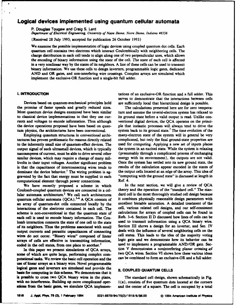
Logical devices implemented using quantum cellular automataP. Douglas Tougaw and Craig S. LentDepartment of Electrical Engmneering Univenity of Notre Dame, Notre Dame. Indiana 46556
(Received 28 July 1993; accepted for publication 26 October 1993)
We examine the possible implementation of logic devices using coupled quantum dot cells. Eachquantum cell contains two electrons which interact Coulombically with neighboring cells. Thecharge distribution in each cell tends to align along one of two perpendicular axes, which allowsthe encoding of binary information using the state of the cell. The state of each cell is affectedin a very nonlinear way by the states of its neighbors. A line of these cells can be used to transmitbinary information. We use these cells to design inverters, programmable logic gates, dedicatedAND and OR gates, and non-interfering wire crossings. Complex arrays are simulated whichimplement the exclusive-OR function and a single-bit full adder.
I. INTRODUCTION tations of an exclusive-OR function and a full adder. Thisserves to demonstrate that the interactions between cells
Devices based on quantum-mechanical principles hold are sufficiently local that hierarchical design is possible.the promise of faster speeds and greatly reduced sizes. The calculations presented here are for zero tempera-Most quantum device designs examined have been similar ture and assume the szveral-electron system has relaxed toto classical device implementations in that they use cur- its ground state before a valid output is read. Unlike con-rents and voltages to encode information. Thus although ventional digital devices, the QCA operates on the princi-the device operations proposed have been based on quan- pie that inelastic processes will always tend to drive thetum physics, the architectures have been conventional, system back to its ground state.7 The time evolution of the
Employing quantum structures in conventional archi- many-electron state of the system will in general be verytectures has proven problematic for reasons directly related complicated, but only the final ground-state properties areto the inherently small size of quantum-effect devices. The used for computing. Applying a new set of inputs placesoutput signal of such ultrasmall devices, which is typically the system in an excited state. While the system is relaxingnanoamperes of current, must be able to drive several other (presumably through a complicated process of exchangingsimilar devices, which may require a change of many mil- energy with its environment), the outputs are not valid.livolts in their input voltages. Another significant problem Once the system has settled into its new ground state, theis that the capacitance of interconnecting wires tends to results of the calculation appear encoded in the states ofdominate the device behavior.' The wiring problem is ag- the output cells located at an edge of the array. This idea ofgravated by the fact that energy must be supplied to each "computing with the ground state" is discussed at length incomputational element through power connections. Ref. 4.
We have recently proposed a scheme in which In the next section, we will give a review of QCACoulomb-coupled quantum devices are connected in a cel- theory and the operation of the "standard cell." The stan-lular automata architecture.2 We call such architectures dard cell is the most thoroughly studied cell design becausequantum cellular automata (QCA). 3 4 A QCA consists of it combines physically reasonable design parameters withan array of quantum-dot cells connected locally by the excellent bistable saturation. A detailed treatment of theinteractions of the electrons contained in each cell. The cell, various related cell designs, and our self-consistentscheme is non-conventional in that the quantum state of calculations for arrays of coupled cells can be found ineach cell is used to encode binary information. The Cou- Refs. 3-6. Section II D discussed how lines of cells can belomb interaction connects the state of one cell to the state used to transmit information using a QCA binary wire.of its neighbors. Thus the problems associated with small Section III shows a design for an inverter, and Sec. IVoutput currents and parasitic capacitances of connecting deals with the influence of several neighboring cells on thewires do not occur. "Binary wires" composed of linear cell states. This leads to the idea of the majority voting
arrays of cells are effective in transmitting information, logic gate and we demonstrate how its behavior can becoded in the cell states, from one place to another.' used to implement a programmable AND/OR gate. Sec-
In this paper we present simulations of QCA arrays, tion V demonstrates a noninterfering planar crossing 4of
some of which are quite large, performing complex coin- two QCA wires. Section VI shows how these various ideas
putational tasks. We review the basic cell operation and the can be combined to form an exclusive-OR and a full adder.
use of linear arrays as a binary wire. Novel programmablelogical gates and inverters are simulated and provide the 11. COUPLED QUANTUM CELLSbasis for computing in this scheme. We demonstrate that itis possible to cross two QCA binary wires in the plane, The standard cell design, shown schematically in Fig.with no interference. Building up more complicated oper- 1 (a), consists of five quantum dots located at the cornersation from the basic gates, we simulate QCA implemen- and the center of a square. The cell is occupied by a total
1615 J. AppL. Phys. 75 (3), 1 Februry 1994 0021.8979/94/75(3)/1818/8/S6.00 @ 1994 American Insl of Physics

Coupled finite element/boundary element method for semiconductorquantum devices with exposed surfaces
Minhan Chen and Wolfgang PorodDepartment of Electrical Engineering Uniersity of Notre Dame, Notre Dame. Indiana 46556
David J. KirknerDepartment of Civil Engineering and Geological ScienceX University of Notre Dame, Notre Dame,Indiana 46556
(Received 21 June 1993; accepted for publication I I November 1993)
We present a study of the boundary conditions for the potential at exposed semiconductorsurfaces in split-gate structures, which views the exposed surface as the interface between thesemiconductor and air. A two-dimensional numerical algorithm is presented for the couplingbetween the nonlinear Poisson equation in the semiconductor (finite element method) andLaplace's equation in the dielectric (boundary element method). The utility of the couplingmethod is demonstrated by simulating the potential distribution in an n-type AIGaAs/GaAssplit-gate quantum wire structure within a semiclassical Thomas-Fermi charge model. We alsopresent a comparison of our technique to more conventional Dirichlet and Neumann boundaryconditions.
I. INTRODUCTION simulates surface Fermi-level pinning at a characteristicenergy level in the band gap,9-1
Recent advances in nanostructure fabrication havemade it possible to realize semiconductor quantum devices ls= -- 6r. (2)by further confining a two-dimensional layer of electronsinto wires or dots in which quantum effects are This approximation leads to an unrealistic discontinuoussignificant. 1.2 Typically, such device structures are defined step in the potential energy at the edge of the biased gateby metallic split gates as schematically depicted in Fig. 1. between the values of the applied gate potential and theIn order to understand the potential distribution in these Fermi-level pinning. Another commonly used approach isstructures, one has to solve the Poisson equation in the to employ a Neumann boundary condition where one as-two-dimensional problem domain, sumes a certain value for the outward normal electric field
on the exposed semiconductor surface,5'6
EV20= -p. (1)
Here, 'k is the confining electrostatic potential, c is the = (3)
dielectric constant of the respective material, and p is thecharge density, which may depend upon the potential and n is the outward normal unit vector of the boundary, e. isfor which different charge models have been developeCL3 the dielectric constant of the semiconductor, and Qit is theSince Eq. (1) is a boundary value problem, one needs to charge density on the exposed surface. It can be shown thatknow the values of the potentials and/or fluxes at the var- this approximation is only valid if the exposed semicon-ious boundaries. In particular at the exposed semiconduc- ductor surface is large and smooth.12 In typical split-gatetor surface, it has proven difficult to formulate appropriate structures used for quantum devices, the confined electronboundary conditions. This is a crucial problem, especially gas is very close to the exposed semiconductor surface andin nanostructures where the charge carriers reside close to the separation between the split gates is rather small. Thethe surface, and a different choice for the boundary condi- validity of the above two boundary conditions, thus, ap-tion at the exposed surface may result in a noticeable dif- pears doubtful.ference in the confining potential of the quantum device. In this paper, we adopt an alternative viewpoint andHighly accurate models of the potential variation will be develop an algorithm for its implementation: We view asneeded to realize recently proposed computing architec- the natural problem domain the semiconductor and thetures for quantum devices, so-called quantum cellular au- dielectric, as schematically shown in Fig. 2. Thus the arti-tomam, which consist of cells of coupled quantum dots ficial boundary conditions at the exposed semiconductorwhich are occupied by only a few electrons.' surface are replaced by more physical matching conditions
In recent numerical studies,"' the potential variation at the interface between the semiconductor and dielectric.in structures like the one shown in Fig. 1 has been treated We assume that the potential 0 is continuous across thisas a boundary value problem on the semiconductor domain interface and that the jump in the normal electric fluxand various boundary conditions have been assumed on density is equal to the interface charge density,the exposed semiconductor surface. One common ap-proach is to utilize a Dirichlet boundary condition which *Is=•Id, (4)
J. AppL Pht. 75 (5). 1 March 1994 0021-8979/94/75(5)/2545/10/$6.00 0 1994 American Institute of Physics 2545