![CDW arXiv:1805.11560v1 [cond-mat.str-el] 29 May 2018ena as side-e ects such as anomalous metallic behaviour [5], topological phases [6], Anderson localization [7] or Mott insulating](https://static.fdocuments.us/doc/165x107/60748a0883b2414b4672537e/cdw-arxiv180511560v1-cond-matstr-el-29-may-2018-ena-as-side-e-ects-such-as.jpg)
Quantum Anomalous Hall E ect and Related Topological Electronic States · Quantum Anomalous Hall E...
90
Quantum Anomalous Hall Effect and Related Topological Electronic States Hongming Weng, 1, 2 Rui Yu, 3 Xiao Hu, 3, * Xi Dai, 1,2, † and Zhong Fang 1,2, ‡ 1 Beijing National Laboratory for Condensed Matter Physics, and Institute of Physics, Chinese Academy of Sciences, Beijing 100190, China 2 Collaborative Innovation Center of Quantum Matter, Beijing, China 3 International Center for Materials Nanoarchitectonics (WPI-MANA), National Institute for Materials Science, Tsukuba 305-0044, Japan Abstract Over a long period of exploration, the successful observation of quantized version of anomalous Hall effect (AHE) in thin film of magnetically-doped topological insulator completed a quantum Hall trio—quantum Hall effect (QHE), quantum spin Hall effect (QSHE), and quantum anomalous Hall effect (QAHE). On the theoretical front, it was understood that intrinsic AHE is related to Berry curvature and U(1) gauge field in momentum space. This understanding established con- nection between the QAHE and the topological properties of electronic structures characterized by the Chern number. With the time reversal symmetry broken by magnetization, a QAHE system carries dissipationless charge current at edges, similar to the QHE where an external magnetic field is necessary. The QAHE and corresponding Chern insulators are also closely related to other topo- logical electronic states, such as topological insulators and topological semimetals, which have been extensively studied recently and have been known to exist in various compounds. First-principles electronic structure calculations play important roles not only for the understanding of fundamen- tal physics in this field, but also towards the prediction and realization of realistic compounds. In this article, a theoretical review on the Berry phase mechanism and related topological electronic states in terms of various topological invariants will be given with focus on the QAHE and Chern insulators. We will introduce the Wilson loop method and the band inversion mechanism for the selection and design of topological materials, and discuss the predictive power of first-principles cal- culations. Finally, remaining issues, challenges and possible applications for future investigations in the field will be addressed. 1 arXiv:1508.02967v3 [cond-mat.mes-hall] 15 Aug 2015
Transcript of Quantum Anomalous Hall E ect and Related Topological Electronic States · Quantum Anomalous Hall E...

Quantum Anomalous Hall Effect and Related Topological
Electronic States
Hongming Weng,1, 2 Rui Yu,3 Xiao Hu,3, ∗ Xi Dai,1, 2, † and Zhong Fang1, 2, ‡
1Beijing National Laboratory for Condensed Matter Physics,
and Institute of Physics, Chinese Academy of Sciences, Beijing 100190, China
2Collaborative Innovation Center of Quantum Matter, Beijing, China
3International Center for Materials Nanoarchitectonics (WPI-MANA),
National Institute for Materials Science, Tsukuba 305-0044, Japan
Abstract
Over a long period of exploration, the successful observation of quantized version of anomalous
Hall effect (AHE) in thin film of magnetically-doped topological insulator completed a quantum
Hall trio—quantum Hall effect (QHE), quantum spin Hall effect (QSHE), and quantum anomalous
Hall effect (QAHE). On the theoretical front, it was understood that intrinsic AHE is related to
Berry curvature and U(1) gauge field in momentum space. This understanding established con-
nection between the QAHE and the topological properties of electronic structures characterized by
the Chern number. With the time reversal symmetry broken by magnetization, a QAHE system
carries dissipationless charge current at edges, similar to the QHE where an external magnetic field
is necessary. The QAHE and corresponding Chern insulators are also closely related to other topo-
logical electronic states, such as topological insulators and topological semimetals, which have been
extensively studied recently and have been known to exist in various compounds. First-principles
electronic structure calculations play important roles not only for the understanding of fundamen-
tal physics in this field, but also towards the prediction and realization of realistic compounds. In
this article, a theoretical review on the Berry phase mechanism and related topological electronic
states in terms of various topological invariants will be given with focus on the QAHE and Chern
insulators. We will introduce the Wilson loop method and the band inversion mechanism for the
selection and design of topological materials, and discuss the predictive power of first-principles cal-
culations. Finally, remaining issues, challenges and possible applications for future investigations
in the field will be addressed.
1
arX
iv:1
508.
0296
7v3
[co
nd-m
at.m
es-h
all]
15
Aug
201
5

Keywords: anomalous Hall effect; quantum anomalous Hall effect; topological invari-
ants; Chern number and Chern insulators; topological electronic states; first-principles cal-
culation
List of Contents
I. Introduction
I.A. Hall Effect and Anomalous Hall Effect (AHE)
I.B. Berry Phase Mechanism for Intrinsic AHE
II. Quantum Hall Family and Related Topological Electronic States
II.A. Chern Number, Chern Insulator, and Quantum AHE (QAHE)
II.B. Z2 Invariant, Topological Insulator, and Quantum Spin Hall Effect (QSHE)
III.C. Magnetic Monopole, Weyl Node and Topological Semimetal
III. First-Principles Calculations for Topological Electronic States
III.A. Calculations of Berry Connection and Berry Curvature
III.B. Wilson Loop Method for Evaluation of Topological Invariants
III.C. Boundary States Calculations
IV. Material Predictions and Realizations of QAHE
IV.A. Band Inversion Mechanism
IV.B. QAHE in Magnetic Topological Insulators
IV.C. QAHE in Thin Film of Weyl semimetals
IV.D. QAHE on Honeycomb Lattice
V. Discussion and Future Prospects
VI. Acknowledgements
VII. References
2

I. INTRODUCTION
I.A. Hall Effect and Anomalous Hall Effect (AHE)
Edwin H. Hall discovered, in 1879, that when a conductor carrying longitudinal current
was placed in a vertical magnetic field, the carriers would be pressed towards the transverse
side of the conductor, which led to observed transverse voltage. This is called Hall effect
(HE)1, and it was a remarkable discovery, although it was difficult to understand at that
time since the electron was not to be discovered until 18 years later. We now know that
the HE is due to the Lorentz force experienced by the moving electrons in the magnetic
field, which is balanced by a transverse voltage for a steady current in the longitudinal
direction. The Hall resistivity ρxy under perpendicular external magnetic field H (along the
z direction) can be written as ρxy = R0H, where R0 is the Hall coefficient, which can be
related to the carrier density n as R0 = − 1ne
(in the free electron gas approximation). The
HE is a fundamental phenomenon in condensed matter physics, and it has been widely used
as as experimental tool to identify the type of carrier and to measure the carrier density or
the strength of magnetic fields.
In 1880, Edwin H. Hall further found that this “pressing electricity effect” in ferromag-
netic (FM) conductors was larger than in non-magnetic (NM) conductors. This enhanced
Hall effect was then called as the anomalous Hall effect (AHE)2, in order to distinguish it
from the ordinary HE. Later experiments on Fe, Co and Ni3 suggested that the AHE was
related to the sample magnetization M (along z), and an empirical relation for the total
Hall effect in FM conductors was established as4,5
ρxy = R0H +RsM, (1)
where the second term is the anomalous Hall resistivity, and its coefficient Rs is material-
dependent (in contrast to R0, which depends only on carrier density n).
As schematically shown in Fig. 1, if we plot the Hall resistivity ρxy versus external
magnetic field H, we will generally expect a straight line (which crosses the origin of the
coordinates) for NM conductors (see Fig. 1(a)); however, non-linear behavior will be ex-
pected for FM conductors, wherein ρxy increases sharply at low field and crosses over into
a linear region under high field (see Fig. 1(b)). The initial sharp increase of ρxy is due to
3

FIG. 1: (Color online) Typical behaviors of the Hall and anomalous Hall effects. The Hall
resistivity ρxy is plotted versus external magnetic field H. (a) The Hall effect; (b) The
anomalous Hall effect; and (c) The hysteresis loop measured from the anomalous Hall
effect.
the saturation of magnetization of the sample under external field. After the saturation of
magnetization, ρxy will depend on H linearly (for high field region), which is dominated by
the ordinary Hall contribution. Therefore, the slope of the linear part under high field gives
us R0. If we extrapolate this linear part to the zero field limit (H=0), it will not go through
the origin of coordinates, and its intercept on y-axis gives us RsM as can be learned from
Eq. (1). This is a surprising result, which immediately implies two important facts: (1)
A kind of Hall effect can be observed even in the absence of external magnetic field (i.e.,
no Lorentz force); (2) The anomalous Hall resistivity is sensitive to magnetic moment M,
and it has been suggested that this property would be useful for the detection of magnetiza-
tion of conducting carriers, particularly for the cases of weak itinerant magnetism, such as
surface/interface magnetization6, dilute magnetic semiconductors7,8, etc. Experimentally,
measurements are usually done in magnetization loops by scanning the magnetic field from
positive to negative, and a hysteresis loop in the ρxy vs. H relationship is to be expected.
This is very similar to the familiar hysteresis loop observed in the M vs. H curve, as usually
found in FM conductors. The empirical relation Eq. (1) is very simple and widely used.
Unfortunately, its correctness is not well justified. As will be pointed out in a latter part
of this article, the anomalous Hall resistivity may have a very complicated form, which is
usually non-linear in M.
Although the HE and AHE look quite similar phenomenologically, their underlying
4

physics are completely different. The HE is due to the Lorentz force’s influence on the
moving electrons under magnetic field; however the AHE exists in the absence of external
magnetic field, where there is no orbital effect of moving electrons. In other words, why do
the electrons move towards the transverse direction in the absence of Lorentz force? The
mechanism of AHE has been an enigmatic problem since its discovery, a problem that lasted
almost a century. This problem involves concepts deeply related to topology and geometry
that have been formulated only in recent years9–15 after the Berry phase was recognized in
198416.
Karplus and Luttinger provided a crucial step in unraveling this problem as early as
195417. They showed that moving electrons under external electric field can acquire an
“anomalous velocity”, which is perpendicular to the electric field and contributes to the
transverse motion of electrons and therefore to the AHE. This “anomalous velocity” comes
from the occupied electronic states in FM conductors with spin-orbit coupling (SOC). They
suggested that the mechanism leads to an anomalous Hall resistivity proportional to the
square of the longitudinal resistivity: ρxy ∝ ρ2xx. Since this contribution depends only on
the electronic band structures of perfect periodic crystal and is completely independent
of scattering from impurities or defects, it is called intrinsic AHE, and it was not widely
accepted until the concept of Berry phase was well established.
For a long time, two other extrinsic contributions had been considered to be the dominant
mechanisms that give rise to the AHE. Smit18,19 suggested that there always exist defects
or impurities in real materials, which will scatter the moving electrons. In the presence
of SOC and ferromagnetism, this scattering is asymmetric and should lead to unbalanced
transverse motion of electrons. This is called skew scattering, and Smit argued that it is
the main source of the AHE. This mechanism predicted ρxy ∼ ρxx, in contrast with the
intrinsic contribution. Berger20, on the other hand, argued that electrons should experience
a difference in electric field when approaching and leaving an impurity, and this leads to
another asymmetric scattering process called side jump, which also contributes to the AHE.
This mechanism marvelously predicts ρxy ∼ ρ2xx, the same as the intrinsic contribution.
The debates about the origin of AHE lasted for a long time, and no conclusion could
be drawn unambiguously. From the experimental point of view, defects or impurities in
samples are unavoidable and are usually complicated with rich varieties. The contributions
from both intrinsic and extrinsic mechanisms should generally coexist21. Experimentalists
5

have tried hard to distinguish them22–25. The controversy also arises because of a lack of
quantitative calculations that could be compared with experiments.
Still, the discovery of the quantum Hall effect in 1980s26 and the later studies on the
geometric phase27 and the topological properties of quantum Hall states28–30, promoted the
fruitful study of AHE significantly. Around the early years of this century, the intrinsic
AHE mechanism proposed by Karplus and Luttinger was completely reformulated in the
language of Berry phase and topology in electronic structures9–13. It was recognized for
the first time that the so-called “anomalous velocity” originates from the Berry curvature
of occupied eigen wave functions, which can be understood as effective magnetic field in
momentum space. This effective magnetic field modifies the equation of motion of electrons
and leads to the intrinsic AHE9–15. From this understanding, we now know the intrinsic
AHE can be evaluated quantitatively from the band structure calculations, thanks to the
rapid development in the field of first-principles calculations. Detailed calculations for var-
ious compounds portray the contributions from intrinsic AHE in a way that convincingly
confirms the existing experimental results11,12,23,25,31,32, establishing the dominant role of the
intrinsic contribution to the AHE. In the meantime, the extrinsic AHE was also analyzed
carefully14, and it was understood that its contribution dominates for the clean limit case
(rather than the dirty limit), where the deviation of distribution of electronic states from the
equilibrium distribution is significant. In this article, we will not discuss the extrinsic AHE.
For readers who want to learn more details, please refer to the review article by Nagaosa
et al.14 Introduction of the Berry phase mechanism for the understanding of intrinsic AHE
was a big step forward in the field, and it is also the fundamental base for understanding
the quantum anomalous Hall effect (QAHE), which is the main subject of this article.
I.B. Berry Phase Mechanism for Intrinsic AHE
In quantum mechanics, the Berry phase is the quantal phase acquired by the adiabatic
evolution of wave function associated with the adiabatic change of the Hamiltonian in a
parameter space R, with R = (R1,R2, ......,Rm) being the set of parameters (a vector).
Let |n(R)〉 be the n-th eigenstate of the Hamiltonian H(R). The overlap of two wave
6

functions infinitesimally separated by ∆R in the R-space can be evaluated as
〈n(R)|n(R + ∆R)〉 = 1 + ∆R〈n(R)|∇R|n(R)〉 = exp[−i∆R ·An(R)], (2)
where An(R) = i〈n(R)|∇R|n(R)〉 is called the Berry connection. Here An(R) is an
important quantity, because it can be viewed as a vector potential and its curl Ωn(R) =
∇R×An(R), called the Berry curvature, gives an effective magnetic field in the parameter
space R (as will be addressed below). The Berry phase γn can then be defined as the
integral of the Berry connection along a closed loop C in the parameter space, or according
to Stoke’s theorem, equivalently as the integral of Berry curvature on the surface S enclosed
by the adiabatic loop C ≡ ∂S (i.e., the surface with the loop C as boundary):
γn =
∮C
An(R) · dR =
∫S
Ωn(R) · dS, (3)
where the second equality suggests that the Berry phase can also be regarded as the effective
magnetic flux passing through a surface S.
Although the concept of the Berry phase has broad applications in physics, its relevance
to the band structure in solids has been recognized only in limited situations, such as the
quantum Hall effect under a strong magnetic field28 and the calculation of electronic polariza-
tion in ferroelectrics33,34. Here we will show that the Berry phase concept is also important
for understanding intrinsic AHE. In this case, we treat the crystal momentum (k) space as
the parameter space. We consider a crystalline solid with discrete translational symmetry.
The eigen equation of the system is given as H(r)ψnk(r) = εnkψnk(r), where H(r) is the
Hamiltonian, εnk and ψnk(r) are the eigen energy and the eigen wave function, and n is the
band index. Because of the translational symmetry, the eigen wave function ψnk(r) of the
system is k-dependent, where k is the momentum defined in the first Brillouin zone (BZ) of
momentum space. According to Bloch’s theorem, the eigen wave function should take the
form of Bloch state ψnk(r) = eik·runk(r), with unk(r) being the periodic part of the wave
function. Then the eigen equation of the system can be recast as Hk(r)unk(r) = εnkunk(r),
where Hk = e−ik·rHeik·r is the k-dependent Hamiltonian. Following the above discussion,
we can now define the Berry connection and Berry curvature in the parameter (momentum
k) space as
An(k) = i〈unk|∇k|unk〉 (4)
Ωn(k) = ∇k ×An(k) = i〈∇kunk| × |∇kunk〉. (5)
7

These two quantities are crucial in understanding the Berry phase mechanism for intrinsic
AHE. Before we can go further, we have to clarify several important properties of the Berry
connection and Berry curvature.
• Berry connection is gauge dependent: As we have learned from the textbooks of solid
state physics, there exists an arbitrary phase factor for the eigen wave function |unk〉
that is not uniquely determined by the eigen equation of the system. Under a U(1)
gauge transformation, the eigen wave function |unk〉 is transformed into |u′nk〉 as
|u′nk〉 = eiφn(k)|unk〉, (6)
where φn(k) is a real and smooth scalar function of k. It is easy to see that |u′nk〉 is still
the eigen wave function of the system for the same eigen state, i.e., Hk|u′nk〉 = εnk|u′nk〉
is satisfied. However, the corresponding Berry connection will be changed by such a
gauge transformation, becoming
A′n(k) = i〈u′nk|∇k|u′nk〉 = An(k)−∇kφn(k). (7)
If we regard the scalar function φn(k) as a kind of scalar potential in the k-space,
this form of transformation is the same as that of a vector potential of magnetic
field in real space, and therefore the Berry connection An(k) can be viewed as an
effective vector potential in momentum space. The gauge dependence of the Berry
connection suggests that it is not physically observable. However, it becomes physical
after integrating around a closed path (i.e., the Berry phase γn defined in Eq. (3)).
This is because the integration of the second term of Eq. (7) around a closed path will
only contribute an integer multiple of 2π, and the Berry phase γn is therefore invariant
modulo 2π.
• Berry curvature is gauge invariant: This conclusion can be drawn directly from the
factor that ∇k × ∇kφn(k) = 0; therefore Ωn(k) = ∇k × A′n(k) = ∇k × An(k) is
unchanged under the U(1) gauge transformation of Eq. (6). This vector form of Berry
curvature suggests that it can be viewed as an effective magnetic field in momentum
space. It is a gauge invariant local manifestation of the geometric properties of the wave
function in the parameter (k) space, and has been proven to be an important physical
ingredient for the understanding of a variety of electronic properties11,15,27,33,34.
8

• Symmetry consideration: Here we consider two important symmetries in solid state
physics, namely time reversal symmetry (TRS) and inversion symmetry (IS). Following
the above discussion, it is easy to learn that the Berry curvature has the following
symmetry properties:
Ωn(k) = Ωn(−k) for inversion symmetry, (8)
Ωn(k) = −Ωn(−k) for time reversal symmetry, (9)
which suggests that Ωn(k) ≡ 0 for a system with both TRS and IS. They are strong
symmetry constraints, which means that in order to study the possible physical effects
related to the Berry curvature, a system with either broken TRS or broken IS is
generally required. For example, the intrinsic AHE is observed in a ferromagnetic
(FM) system with SOC, where the TRS is broken. For a system with TRS only, in
general Ωn(k) 6= 0, however its integration over the whole Brillouin zone should be
zero as implied by Eq. (9). In such a case, the Berry curvature may take effect only
through k-selective or band n sensitive probes.
• The choice of periodic gauge: For the convenience of studies on solid states with
discrete translational symmetry, we usually use the periodic gauge in practice. That
is, we require the Bloch wave function to be periodic in momentum space, and use
the condition ψk(r) = ψk+G(r) (where G is a translational vector for the reciprocal
lattice) to partly fix the phases of wave functions. This periodic gauge is used in most
of the existing first-principles electronic structure calculation codes. However, we have
to note that it is a very weak gauge-fixing condition, and abundant gauge degrees of
freedom still remain.
• Gauge field: Spreading out each component of the vector form discussed above (Eq.
(5)), the Berry curvature can be written explicitly as an anti-symmetric second-rank
tensor Fµν ,
εµνξΩn,ξ = Fn,µν =∂
∂kµAn,ν(k)− ∂
∂kνAn,µ(k)
= i
[〈∂unk∂kµ|∂unk∂kν〉 − 〈∂unk
∂kν|∂unk∂kµ〉], (10)
9

where εµνξ is the Levi-Civita antisymmetric tensor, and µ, ν, ξ can be simply treated
as the direction indices (i.e., x, y, z) for our purposes. For example, for many of our
following discussions on the transport properties in a two dimensional (2D) system,
we will use the equality,
Ωn,z = Fn,xy. (11)
Writing it in such a way also helps us understand that Berry curvature is simply the
U(1) gauge field (Fµν) in the language of gauge theory. In the presence of gauge
freedom, in order to preserve the gauge invariance of Lagrangian under the gauge
transformation, we need to use the gauge covariant derivative instead of the original
derivative. For example, for the position operator xµ = i∂kµ , its gauge covariant form
is written as xµ = i∂kµ − Aµ(k), where Aµ(k) is the vector potential (i.e., the Berry
connection). In such a case, the gauge covariant position operators xµ and xν are
no longer commutable, and their commutation relation is given as [xµ, xν ] = −iFµν ,
which gives the gauge field Fµν = ∂kµAν − ∂kνAµ.
Keeping in mind all these properties discussed above for the Berry connection and Berry
curvature, we are now ready to understand the intrinsic AHE from the viewpoint of gauge
field and geometric Berry phase. For simplicity, let us first consider a 2D system with
Hamiltonian H0(x, y) defined in the xy-plane. Under an external electric field Ey, the whole
Hamiltonian of the system becomes H(x, y) = H0(x, y) + eEyy. By evaluating the velocity
operator as x = − i~ [x,H] = − i
~ [x,H0]− i~ [x, eEyy], we find that the presence of electric field
in the system leads to an additional velocity term, vx = − i~ [x, eEyy] = − e
~FxyEy = − e~ΩzEy,
which is along the x direction (being transverse to the external electric field Ey). This result
comes from the non-vanishing commutation relation between the gauge covariant position
operators. This additional velocity term is nothing but the anomalous velocity term proposed
by Karplus and Luttinger17, and is the origin of the intrinsic anomalous Hall effect.
Now let us generalize the above discussion to three dimensional (3D) space and consid-
ering both the electric and magnetic external fields, we find that the equation of motion of
electrons, in the presence of gauge field, should be recast as15
r =1
~∂εn(k)
∂k− k×Ωn(k), (12)
k = − e~
(E + r×B), (13)
10
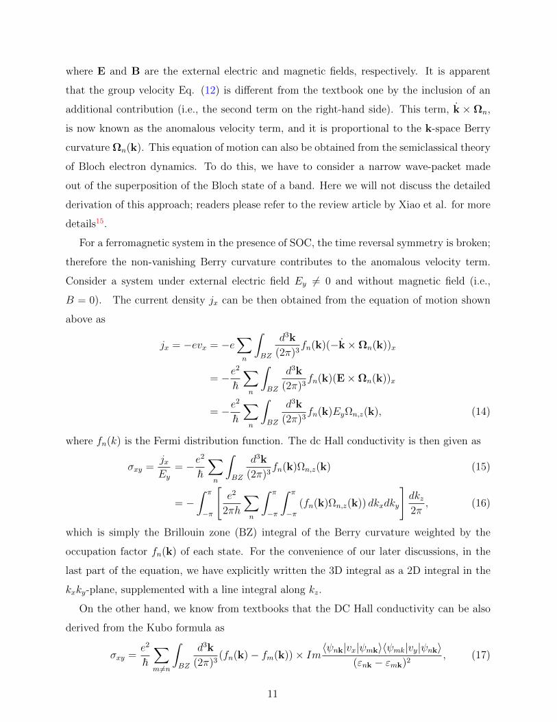
where E and B are the external electric and magnetic fields, respectively. It is apparent
that the group velocity Eq. (12) is different from the textbook one by the inclusion of an
additional contribution (i.e., the second term on the right-hand side). This term, k × Ωn,
is now known as the anomalous velocity term, and it is proportional to the k-space Berry
curvature Ωn(k). This equation of motion can also be obtained from the semiclassical theory
of Bloch electron dynamics. To do this, we have to consider a narrow wave-packet made
out of the superposition of the Bloch state of a band. Here we will not discuss the detailed
derivation of this approach; readers please refer to the review article by Xiao et al. for more
details15.
For a ferromagnetic system in the presence of SOC, the time reversal symmetry is broken;
therefore the non-vanishing Berry curvature contributes to the anomalous velocity term.
Consider a system under external electric field Ey 6= 0 and without magnetic field (i.e.,
B = 0). The current density jx can be then obtained from the equation of motion shown
above as
jx = −evx = −e∑n
∫BZ
d3k
(2π)3fn(k)(−k×Ωn(k))x
= −e2
~∑n
∫BZ
d3k
(2π)3fn(k)(E×Ωn(k))x
= −e2
~∑n
∫BZ
d3k
(2π)3fn(k)EyΩn,z(k), (14)
where fn(k) is the Fermi distribution function. The dc Hall conductivity is then given as
σxy =jxEy
= −e2
~∑n
∫BZ
d3k
(2π)3fn(k)Ωn,z(k) (15)
= −∫ π
−π
[e2
2πh
∑n
∫ π
−π
∫ π
−π(fn(k)Ωn,z(k)) dkxdky
]dkz2π
, (16)
which is simply the Brillouin zone (BZ) integral of the Berry curvature weighted by the
occupation factor fn(k) of each state. For the convenience of our later discussions, in the
last part of the equation, we have explicitly written the 3D integral as a 2D integral in the
kxky-plane, supplemented with a line integral along kz.
On the other hand, we know from textbooks that the DC Hall conductivity can be also
derived from the Kubo formula as
σxy =e2
~∑m6=n
∫BZ
d3k
(2π)3(fn(k)− fm(k))× Im〈ψnk|vx|ψmk〉〈ψmk|vy|ψnk〉
(εnk − εmk)2, (17)
11

which is basically equivalent to Eq. (15), by expanding each term of the vector form of the
Berry curvature explicitly with some algebra. However, we have to emphasize that the form
of Eq. (15) for Hall conductivity is not only compact, but also fundamentally important
for the underlying physics. It demonstrates the Berry phase mechanism of the intrinsic
AHE, and it is the key equation for our following discussions on the geometric meaning and
topological nature of QAHE. For example, for a two dimensional system, the BZ integral
of Berry curvature for a fully occupied band must give rise to an integer multiple of 2π.
Therefore, the Hall conductivity σxy for a 2D insulator can be finite and be an integer
multiple of e2/h. This is the underlying physics for the quantization of the AHE.
In addition to the understanding of the Berry phase mechanism for the intrinsic AHE
discussed above, another important step forward in this field is the quantitative and accu-
rate evaluation of the anomalous Hall conductivity (AHC) for realistic materials, yielding
results that can be compared with experimental observations. Due to the rapid increase
of computational power and the development of first-principles calculation methods, such
quantitative comparisons (though still difficult) become possible and contribute greatly to
the development of the field. In a series of papers reporting quantitative first-principles
calculations for SrRuO311, Fe12 and CuCr2Se4−xBrx
31, it was demonstrated that the calcu-
lated AHC can be reasonably compared with experiments, suggesting the importance of the
intrinsic AHE. In more recent years, accurate calculations of AHC have been achieved by
using the Wannier function interpolation scheme35,36. The presence of SOC and the breaking
of TRS are crucially important for the intrinsic AHE in those systems.
In summary of this part, we have discussed the Berry phase mechanism for intrinsic AHE.
Conceptually, this is an important increment in our understanding because the intrinsic
AHE is now directly linked to the geometric and topological properties of the Bloch states
in momentum space. This understanding has also led to a great number of research projects
on the exotic properties of electronic systems with SOC, such as QAHE and the topological
insulators.
12

II. QUANTUM HALL FAMILY AND RELATED TOPOLOGICAL ELECTRONIC
STATES
One of the main subjects of condensed matter physics is the study and classification of dif-
ferent phases and various phase transitions of materials that possess rich varieties of physical
properties. Landau developed a general symmetry-breaking theory to understand the phases
and phase transitions of materials. He pointed out that different phases really correspond
to different symmetries of compounds. An ordered phase, in general, can be described by a
local order parameter, and the symmetry of the system changes as a material changes from
one phase to another. Landau’s symmetry-breaking theory is very successful in explaining a
great many kinds of phases (or states) in materials, but it does not work for the topological
quantum states. A topological quantum state cannot be described by a local order parame-
ter, and it can change from one state to another without any symmetry-breaking. Topology,
a word mostly used in mathematics, is now used to describe and classify the electronic struc-
tures of materials. “Topological electronic state” means an electronic state which carries
certain topological properties (in momentum space usually), such as the states in topological
insulators37–54, topological semimetals55–72, topological superconductors49,50,73–79, etc. One
of the most important characteristics of topology is the robustness against local deforma-
tions, or in the language of physics, the insensitivity to environmental perturbations, which
makes topological electronic states promising for future applications. To characterize the
order of topological states, new parameters, namely the topological invariants, are needed.
In this section, we will review some of the topological electronic states and their quan-
tum physics, including the integer quantum Hall (IQH) state, the quantum anomalous Hall
(QAH) state, the quantum spin Hall (QSH) state, and the topological semimetal (TSM)
state. We will use the concept of Berry phase in momentum space to discuss the topological
nature of topological states and the related topological invariants.
II.A. Chern Number, Chern Insulator, and Quantum AHE
In 1980, Klaus von Klitzing discovered26 that the Hall conductance, viewed as a function
of strength of the magnetic field applied normal to the two-dimensional electron gas plane,
at very low temperature, was quantized and exhibited a staircase sequence of wide plateaus.
13
The values of Hall conductance were integer multiples of a fundamental constant of nature:
e2/h = 1/(25812.807572 Ω), with totally unanticipated precision, and independent of the
geometry and microscopic details of the experiment. This is an important and fundamental
effect in condensed matter physics, and it is called the integer quantum Hall effect (IQHE)
— the quantum version of the Hall effect.
The IQHE is now well understood in terms of single particle orbitals of an electron in
a magnetic filed (i.e., the Landau levels), and the phenomenon of “exact quantization” has
been shown to be a manifestation of gauge invariance. The robustness and the remarkable
precision of Hall quantization can also be understood from the topological nature of the
electronic states of 2D electron gas under magnetic field. The integer number, originally
known as the TKNN number28 in the Hall conductance derived from the Kubo formula,
is now characterized as a topological invariant called “Chern number”. This topological
understanding of the IQHE is a remarkable leap of progress, opening up the field of topo-
logical electronic states in condensed matter physics. IQHE is therefore regarded as the first
example of topologically non-trivial electronic states to be identified and understood.
This conceptual breakthrough with regard to the topological nature of IQHE, though
important, was not widely generalized, and the relationship of IQHE to the rich variety of
condensed materials was not revealed for a long time. This is because the IQHE is observed
only in a very particular system, i.e. 2D electron gas under strong external magnetic field,
and the formation of Landau levels (usually at very low temperature) is required. Under
such extreme conditions, the material’s details and its electronic band structure become
irrelevant to the physics. In this sense, the lattice model proposed by Haldane in 198837 is
very stimulating for the study of topological electronic states. He proposed that a spinless
fermion model on a periodic 2D honeycomb lattice without net magnetic flux can in principle
support a similar IQHE. Although Haldane’s model is very abstract and unrealistic (at least
at that time), his result suggested that a kind of quantized Hall effect can exist even in
the absence of magnetic field and the corresponding Landau levels. In other words, certain
materials, other than the 2D electron gas under magnetic field, can have topologically non-
trivial electronic band structures of their own, which can be characterized by a non-zero
Chern number. Such materials were called Chern insulators later. In this way, the concept
of topological electronic state was generalized and was connected to the electronic band
structure of materials.
14

The progress in the study of IQHE was very inspiring in the 1980s; on the other hand,
not much of it was related to the field of AHE. Around that time, the development of the
AHE field was rather independent, with almost no intersection with the study of IQHE. But
the understanding of Berry phase mechanism for intrinsic AHE9–13, reformulated around
the early years of the 21st century, changed the situation significantly. This understanding
established the connection between the AHE and the topological electronic states. By this
connection, it is now understood10,11,80 that intrinsic AHE can have a quantum version —
the quantum anomalous Hall effect (QAHE), which is in principle similar to IQHE but
without external magnetic field and the corresponding Landau levels. It turns out that this
is exactly the same effect discussed by Haldane for a Chern insulator with a non-zero Chern
number. Currently, the fields of IQHE and AHE are closely combined, and the realization of
a Chern insulator becomes possible by finding the QAHE in suitable magnetic compounds
with strong SOC.
The IQHE and the QAHE have their own characteristics; however, their underlying
physics, in terms of the topological properties of their electronic structures, are basically
the same. They are all related to the Berry connection, Berry curvature and Berry phase in
momentum space, as discussed in the previous section. In this part, we will not discuss the
particular details associated with each effect, but rather we will concentrate on their common
features, namely the topological property and topological invariant (Chern number). To
begin with, we will discuss several important concepts:
• Hall Conductivity as Integral of Berry Curvature: Considering a 2D insulating system
with broken TRS, the Hall conductivity of the system at low enough temperature can
be written as
σxy = −e2
~∑n
∫BZ
d2k
(2π)2fn(k)Ωn,z(k)
= − e2
2πh
∫BZ
d2k∑n(occ)
Ωn,z(k)
= − e2
2πh
∫BZ
d2kΩz(k), (18)
where the second equality follows because of the existence of an energy gap and fn(k) =
1 (=0) for the occupied (unoccupied) state (see Eqs. (14)-(16) for a 3D version). This
form of Hall conductivity can be derived either from the Berry phase formalism or
15
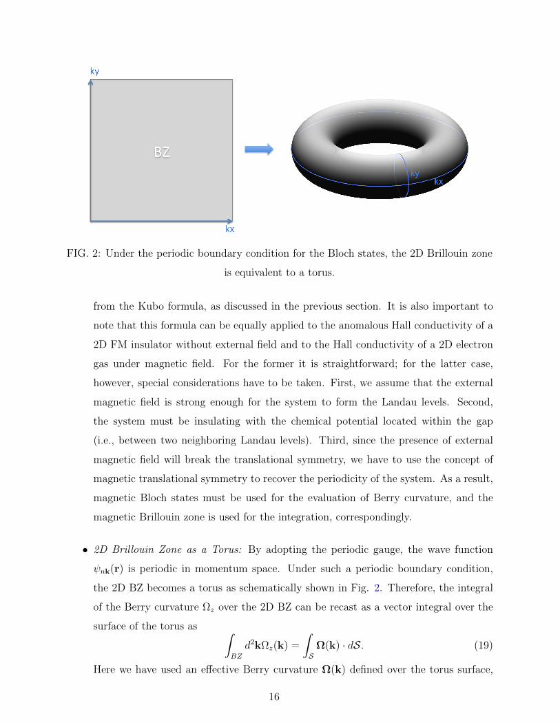
FIG. 2: Under the periodic boundary condition for the Bloch states, the 2D Brillouin zone
is equivalent to a torus.
from the Kubo formula, as discussed in the previous section. It is also important to
note that this formula can be equally applied to the anomalous Hall conductivity of a
2D FM insulator without external field and to the Hall conductivity of a 2D electron
gas under magnetic field. For the former it is straightforward; for the latter case,
however, special considerations have to be taken. First, we assume that the external
magnetic field is strong enough for the system to form the Landau levels. Second,
the system must be insulating with the chemical potential located within the gap
(i.e., between two neighboring Landau levels). Third, since the presence of external
magnetic field will break the translational symmetry, we have to use the concept of
magnetic translational symmetry to recover the periodicity of the system. As a result,
magnetic Bloch states must be used for the evaluation of Berry curvature, and the
magnetic Brillouin zone is used for the integration, correspondingly.
• 2D Brillouin Zone as a Torus: By adopting the periodic gauge, the wave function
ψnk(r) is periodic in momentum space. Under such a periodic boundary condition,
the 2D BZ becomes a torus as schematically shown in Fig. 2. Therefore, the integral
of the Berry curvature Ωz over the 2D BZ can be recast as a vector integral over the
surface of the torus as ∫BZ
d2kΩz(k) =
∫S
Ω(k) · dS. (19)
Here we have used an effective Berry curvature Ω(k) defined over the torus surface,
16

which satisfies the condition Ω(k) · n = Ωz(k), where n is the unit vector along the
normal of the surface S.
• Quantization and Chern Number: The torus is a closed manifold without boundary,
so according to Chern’s theorem81 in differential geometry, the vector integral of Berry
curvature over a torus surface must be an integer multiple of 2π,∫S
Ω(k) · dS = 2πZ, (20)
where Z is an integer number called Chern number. Having this property, it is now
easy to see that the Hall conductivity for a 2D insulator must be quantized as
σxy = − e2
2πh× 2πZ = −e
2
hZ. (21)
• Absence of Smooth Gauge: Based on Stokes’ theorem, the surface integral of Berry
curvature (Eq. (20)) can also be evaluated as an loop integral of the Berry connection
A(k) along the boundary of the BZ, i.e.,∫S Ω(k) · dS =
∮CA(k) · dk. Since the BZ
is a torus, which has no boundary, the integral must be vanishing if A(k) is smoothly
defined in the whole BZ. Therefore, a non-zero Chern number indicates that we cannot
choose a smooth gauge transformation such that A(k) is continuous and single valued
over the whole BZ. Thus, non-zero Chern number can be viewed as obstruction to
continously define the phase of the occupied wave functions on a 2D BZ, which is a
torus.82–84.
For a system with multiple bands, the Berry curvature should be understood as the
summation of contributions coming from all occupied bands. Having the properties discussed
above, we can now define a Chern insulator as a 2D insulator whose electronic structure gives
a non-zero Chern number. The above discussions about the Chern number and the topology
of electronic states in momentum space may be still too abstract, in the following we will
give a more explicit explanation, in which the none zero Chern number manifests itself as the
winding number of the Wannier center evolution for the effective 1D systems with constant
ky. Here we consider the simplest case: a 2D lattice with only one single occupied band
(the band index n can therefore be neglected). Although it is impossible to choose a single
smooth gauge over the whole BZ for a Chern insulator according to our above discussions,
17

it is possible to choose a special gauge that is smooth and periodic along one direction (say
kx), but not necessarily along the other (say ky)82–85. Thus, we can do the integration in Eq.
(19) explicitly for the kx direction with fixed ky and obtain (we set the lattice parameter
a=1)
2πZ = −∫ π
−π
∫ π
−πdkxdky(∂kxAy − ∂kyAx)
=
∫ π
−πdky∂ky
(∫ π
−πdkxAx(kx, ky)
)=
∫ π
−πdθ(ky). (22)
FIG. 3: The evolution of θ(ky) (or 1D Wannier center) on cylinder surface for system with
(a) Z=0, (b) Z=1 and (c) Z=2.
Here, θ(ky) =∫ π−π dkxAx is an angle (i.e., Berry phase) calculated from the 1D integration
of Ax(kx, ky) along the kx axis (a closed loop) for each fixed ky. We can then plot θ(ky) as
18

a function of ky. As shown in Fig. 3, over a cylinder surface (in the cylinder coordinates),
ky is along the longitudinal direction, and the azimuth is the angle θ(ky) for each fixed ky.
Moving from ky=−π to ky=π, we can see the difference between the trivial insulator (Z=0)
and the Chern insulator (Z 6= 0). The winding number of θ(ky) over the cylinder surface is
zero for the former (Fig. 3(a)), and non-zero for the latter (Fig. 3(b), (c)). In this way, we
relate the Chern number to some kind of winding number defined by the eigen functions,
and see that the Chern insulator has a “twisted” energy band.
It is also interesting to note that the ky-dependent Berry phase calculated as
Pn(ky) =θn(ky)
2π=
1
2π
∫ π
−πdkxAn,x(kx, ky) (23)
can be related to the Wannier center of a 1D system (where we have recovered the band
index n dependence). To see this, we consider a generic 2D system and denote the Wannier
function in cell R associated with band n, given in terms of the Bloch states, as
|nR〉 =1
(2π)2
∫BZ
d2ke−ik·R|ψnk〉, (24)
with
|ψnk〉 =∑R
eik·R|nR〉, (25)
where k = (kx, ky) is considered, and the periodic part of the Bloch function is defined as
unk(r) = e−ik·rψnk(r). (26)
Then the matrix elements of the position operator r between Wannier functions take the
form
〈nR|r|m0〉 = i1
(2π)2
∫BZ
d2keik·R〈unk|∇k|umk〉, (27)
from which we get the center of the Wannier function in the 0-th cell as
r = 〈n0|r|n0〉 = i1
(2π)2
∫BZ
d2k〈unk|∇k|unk〉. (28)
Now let us consider the kx and ky directions separately, and define the 1D Wannier
function for each fixed-ky as
|n,Rx, ky〉 =1
(2π)
∫ π
−πdkxe
−ikxRx|ψnk〉. (29)
19

Then the 1D Wannier center (along x direction) as function of ky can be defined as the
average value of position operator x as
x(ky) = 〈n,Rx = 0, ky|x|n,Rx = 0, ky〉 =i
(2π)
∫ π
−πdkx〈unk|∇kx|unk〉 = Pn(ky), (30)
from which we see that Pn(ky) is nothing but the 1D Wannier center of band n. The
Chern number can therefore be understood as the winding number of 1D Wannier center
when it evolves as a function of ky (see Fig. 3). We can also see that when the Chern
number is not zero, we cannot choose a smooth gauge transformation such that A(k) is
continuous and single valued over the whole BZ. Although the above discussion is only for
the simplest systems with single occupied band, generalization to the multi-band situation is
quite straightforward. For a general band insulator with multiple occupied bands, the Berry
connection Anm(k) = i〈unk|∇k|umk〉 contains band index n, m and becomes nonabelian
Then the Berry curvature that defines the Chern number is obtained from the trace of the
Berry connection A(k).
The Hall conductivity of a Chern insulator with a non-zero Chern number must be
quantized as an integer multiple of e2
h. Different Chern numbers give different states whose
Hall conductivities are different, but their local symmetry can be the same. Therefore, to
distinguish the states, we cannot use local order parameters (in the language of Landau’s
symmetry breaking theory); instead we need a topological invariant, the Chern number, as a
global order parameter of the system. By rewriting Hall conductivity in terms of the Berry
curvature and Berry phase, we can now unify QHE and QAHE. Readers will recall that the
QAHE is nothing but the quantum version of the AHE realized in a Chern insulator without
the presence of external magnetic field.
Similar to QHE, where the TKNN number is related to the number of edge states in a real
2D sample with boundary28, the Chern number can also be physically related to the number
of edge states for a 2D Chern insulator37. The existence of edge states is a direct result
of the topological property of the bulk electronic structure, and is due to the phenomenon
discussed in the literature as the bulk-boundary-correspondence86,87. In this case, due to the
broken TRS, the edge state must be chiral (i.e, the electrons of the edge state can move only
in one direction surrounding the sample boundary, either left- or right-handed, as shown in
Fig. 4(b)). As discussed with regard to IQHE, the charge transport of the edge state is in
principle dissipationless, and back-scattering is absent due to the lack of an edge state with
20

FIG. 4: Schematic illustrations of the edge states in (a) QHE; (b) QAHE, and (c) QSHE.
opposite velocity88,89.
Although the topological properties of Chern insulators and the related QAHE are fun-
damentally the same as that discussed with regard to IQHE, they are conceptually broadly
generalized to a wide field and to a rich variety of materials. This generalization is an impor-
tant step forward, providing the building blocks for subsequent discussions of many possible
topological electronic states. From the application point of view, the Chern insulator (or the
related QAHE) is also important because the quantized Hall conductivity can be realized in
the absence of magnetic field, greatly simplifying measurement conditions.
II.B. Z2 Invariant, Topological Insulator, and Quantum Spin Hall Effect
(QSHE)
Although the Chern insulator (or the related QAHE) is the simplest topological electronic
state, its realization occurred rather later and was much stimulated by the rapid develop-
ment in the field of topological insulators—another interesting topological electronic state
protected by TRS. Considering symmetry, it is easy to prove that the Chern number in Eq.
(20) must be vanishing for an insulator with TRS. However, this does not mean that the
electronic state carries no topological property in this case. Kane and Mele38 introduced a
new topological invariant, the Z2 number, to classify an insulating system with TRS. They
proposed that a time reversal invariant insulator can be further classified as a trivial in-
sulator with Z2 = 0 or a non-trivial topological insulator with Z2 = 1, which is a typical
example of a symmetry protected topological state90. A Z2 topological insulator in 2D is
also called a quantum spin Hall insulator (QSHI) because it can support the quantum spin
Hall effect (QSHE)39–42, which shares certain features with the IQHE and QAHE and can
be understood from the viewpoint of “band-twisting” or winding number of Berry phase
21

in momentum space. A QSHI is different from a trivial insulator in the sense that it has
gapped insulating states in the bulk but gapless states on the edge due to its topological
property. It is also distinguished from the Chern insulator in the sense that QSHI has
even number of edge states, composed of pairs of counter-propagating chiral edge states,
as shown in Fig. 4(c)). The QSHE has been explicitly discussed for graphene lattice39 and
HgTe quantum well structures40–42. In this part, however, we will take a simple task and
discuss the Z2 invariant and the topological state with TRS from the viewpoint used above
for the Chern insulator.
For a 2D insulator with TRS, the total number of occupied electronic states must be
even. Suppose we can divide them into two subspaces, I and II , which are related by TRS
and smoothly defined on the whole BZ. Evaluating the Chern number for each subspace
independently, if one has Chern number Z, the other one must have Chern number -Z (due
to the TRS) and the total Chern number of the whole system is always zero. It seems
that we can use Z as the topological index to classify the band insulators with TRS. While
unfortunately, the smooth partition of the occupied states into two subspaces with one being
the time reversal of another is only possible with extra good quantum numbers, such as Sz,
where the Chern number obtained within the spin up subspace can be used to describe the
topology of the system and is called “spin Chern number”. But generically such a smooth
partition of the occupied states can only be made for half of the BZ (not the whole BZ)
and we need at least two patches (A and B) to fully cover the whole BZ. The winding
number of the U(2N) gauge transformation matrix tAB(k) at half of the boundary between
two patches can be used to define a new classification of the band insulators with TRS. As
further proved by Fu and Kane, only the even and odd feature of the above winding number
is unchanged under the U(2N) gauge transformation and all the band insulators with TRS
can be classified into topological trivial and non-trivial classes, which is called Z2 invariance
accordingly. Fu and Kane further derived the expression for Z2 invariance in terms of both
Berry connection and Berry curvature as91
Z2 =1
2π
(∮∂(BZ/2)
A(k) · dk−∫BZ/2
d2kΩz(k)
)mod 2, (31)
where integral of Berry curvature is performed over the half BZ (i.e., BZ/2), and the integral
of Berry connection is performed along the boundary of the half BZ (i.e., ∂(BZ/2)). To
evaluate Z2 invariance using the above equation, one needs to find a smooth gauge for the
22

wave functions on half of the BZ, which is very difficult for the band structure calculations for
realistic materials, and as a result, this formula is rarely used in practice. On the other hand,
the Z2 invariance is a gauge invariant quantity, one should be able to compute it without
any gauge fixing condition. For that purpose, some of the authors of the present paper
developed an alternative expression for the Z2 invariance called Wilson loop method, which
will be introduced in detail in section 3.2. Here we just sketch its main idea briefly. Similar
with the Wilson loop method for Chern number calculation, the purpose of the Wilson loop
method is to calculate the “Wannier center” of each band for the effective 1D insulators with
fixed ky and determine the Z2 invariance by looking at their evolution with ky. With the
presence of TRS, a generic system contains 2N occupied bands. As mentioned previously,
now the Berry connection becomes 2N*2N matrix. The loop integral of such U(2N) Berry
connection gives a 2N*2N unitary matrix D(ky). The U(1) part of this matrix contributes
to the Chern number as discussed before and the Z2 invariance can be obtained from the
remaining SU(2) part by taking the phases of its eigenvalues θn(ky), where n denotes the
band index. As proved in Ref. 92, the TRS only guarantees the double degeneracy of θn(ky)
at two time reversal invariant loops ky = 0 and ky = π. The Z2 invariance of the system is
determined by whether the θn(ky)s switch parters or not as they evolves from ky = 0 to π.
To be explicit, let us again consider the simplest example of 2D insulator, with only
two occupied bands, ψI,k and ψII,k, which are related by the TRS (say, for example,
ψI,−k=TψII,k, where T is the time reversal operator). The two states form a Kramers
pair and must be degenerate at the time-reversal-invariant momentum (TRIM) of the BZ
(i.e, with kx or ky = 0, π). We can evaluate θ(ky) for all occupied bands (as we have done
above for the Chern insulator). As mentioned previously, the two Wannier centers must be
degenerate at ky = 0 and π, which leads to three situations in general (as shown in Fig.
5(a)-(c)). First, if the evolution path of the θ(ky) doesn’t enclose the half BZ, this is the
trivial situation with Z2 invariance ν=0 (Fig. 5(a)). Second, if the evolution path of the
θ(ky) enclose the half BZ once, this is the non-trivial topological insulator with Z2 index
ν=1, where the crossing of two θ(ky) curves at ky = 0 and π is protected by the TRS (Fig.
5(b)). Third, if the evolution path of the θ(ky) enclose the half BZ twice, the two θ(ky)
curves must cross at some ky other than the TRIM. Such crossings are not protected by the
TRS and are removed by small perturbations, which drive the crossings into anti-crossings.
As the result, the system becomes equivalent to the trivial case with Z2 index ν =0 (Fig.
23

FIG. 5: Evolution of Wannier centers (Pn(ky)) for systems with (a) Z2=0, (b) Z2=1, (c)
|Z|=2 but Z2=0. The Wannier centers wind the cylinder surface even (a, c) and odd (b)
times respectively. Figure from Ref. 92
5(c)).
The edge states of 2D Z2 topological insulators must appear in pairs due to the existence of
TRS, and each pair of edge states is composed of two counter-propagating chiral edge states,
which are related to each other by the TRS. In this case, if one state at the edge has velocity
v, we can always find another state with opposite velocity −v. However, back-scattering
between the two states is again forbidden because the two states must have opposite spins.
Existence of such pair of edge states leads to the observable QSHE38,39,41, where the spin
Hall conductivity is quantized in units of e2π
(if Sz is conserved). According to our above
discussions of the Z2 topology, if there exist multiple pairs of edge states, two pairs can in
principle couple together and open up a gap (because scattering between the pairs is not
24

forbidden). As a result, the Z2 number is physically related to the number of pairs of edge
states mod 2, in contrast to the case of Chern insulators.
Using the 2D topological invariants (such as Z or Z2) as building blocks, a 3D crystal
can in principle be characterized by a triplet of 2D topological numbers for the three crystal
orientations, respectively. In such a way, we can extend the topological classes from 2D to
3D. There are in general two situations by doing this: (1) one is the trivial extension leading
the “weak” 3D topological class, which can be viewed as a simple stacking of 2D topological
insulating layers along a certain crystal orientation; (2) another is a non-trivial extension
leading to a “strong” topological class, which is a new and stable topological state in 3D.
For example, by a simple stacking of 2D Chern insulating layers along the z direction, if the
band dispersion along kz is weak enough, each 2D layer with fixed kz will keep its original
topological property (characterized by a non-zero Chern number). As a result, a 3D “weak”
Chern insulator can be obtained. In a similar way, a 3D “weak” topological insulator can
be obtained too. However, it is important to note that, if we concentrate on insulators only,
there will be no “strong” Chern insulator in 3D; on the other hand, a new 3D state with
TRS, called “strong” topological insulator, can be obtained93–95 by extending the Z2 number
from 2D to 3D. (As will be discussed in the next section, the missing “strong” Chern class
in 3D has to be a metal—the topological semimetal).
For a 3D insulator with TRS, there will be 8 TRIM points in the BZ (different from 2D BZ
which has only 4 TRIM points). For any 4 TRIM points that lie in the same plane, we can
define a 2D Z2 number as discussed above. In total, there will be 16 invariant configurations
and can be distinguished by four independent Z2 indices, ν0(νxνyνz), as discussed in Ref. 93.
Here ν0 is the total Z2 number, and the νx,y,z are the 2D Z2 numbers along the x, y, z
directions, respectively. The three weak Z2 indices νx,y,z can be evaluated for the kx = π,
ky = π, and kz = π planes, as a convention, respectively. The total Z2 index ν0, however, is
a strong index, and it has to be evaluated globally by considering the 3D structure. That is,
we have to consider the change of 2D Z2 number between two parallel planes (perpendicular
to certain reciprocal lattice vector). For example, we can choose the kx=0 and π planes, or
ky=0 and π planes, or kz=0 and π planes. If the Z2 numbers of two planes are different,
we have ν0 = 1, otherwise, if they are the same, we have ν0 = 0. A realistic example will
be given in Section 3. For a 3D strong topological insulator with strong topological index
ν0 6= 0, on its boundary (i.e, surface), we will expect the Dirac cone type surface states,
25

which are protected by the TRS49,50.
II.C. Magnetic Monopole, Weyl node and Topological Semimetal
As mentioned above, if we attempt to consider the possible “strong” topological state
characterized by Chern numbers in 3D, we will find that it has to be a metal, and this leads
to a very interesting new topological state of quantum matters — topological metals or
semimetals. We will see that this is a much more general state, and the 2D Chern insulating
state can be regarded as a special cut of the 3D topological semimetal state along a certain
plane in momentum space. From another point of view, we can also raise a question like
the following. Since we know from the above discussions that insulators can be further
classified as topologically trivial and non-trivial insulators, can we do the same classification
for metals? If possible, what will be the topological invariant for the proper description of
the topological metallic state? This is a very interesting question, and we will show in this
part that it is related to the magnetic monopoles11,96 and Weyl nodes in momentum space.
Berry phase is called quantum geometric phase since it has a very intuitive geometric
picture. It is proportional to the solid angle subtended at the magnetic monopole by the
adiabatic loop of Hamiltonian in momentum space. The magnetic monopole is the source
or drain of the gauge field Ωn(k). Since
Ωn(k) = −Im∑m 6=n
〈um|∇kH(k)|un〉 × 〈un|∇kH(k)|um〉(Em(k)− En(k))2
, (32)
it diverges at the point k = k0 where Em(k0)=En(k0) (see Eqs. (16) and (17)). This means
that the magnetic monopole is formed by energy level crossing, and a two-energy-level system
is the simplest case. Consider the generic form of the Hamiltonian for any two-level system,
H = d0(k)I2×2 + d(k) · σ, (33)
where I2×2 is the identity matrix, d is a 3D vector depending on momentum k, and σ are
Pauli matrices. There are two eigen states ψ± with eigen energies E± = d0(k) ±√
d · d.
The term d0(k) is just a shift of zero energy level, and can be neglected. At the energy
degeneracy or level crossing point (k = k0), E+=E− (i.e, d(k0)=0) is required. Obviously,
k0 is not necessarily on the path of a adiabatic loop change of the Hamiltonian, which means
that the band gap between E+ and E− can be well preserved if the Fermi level is away from
26
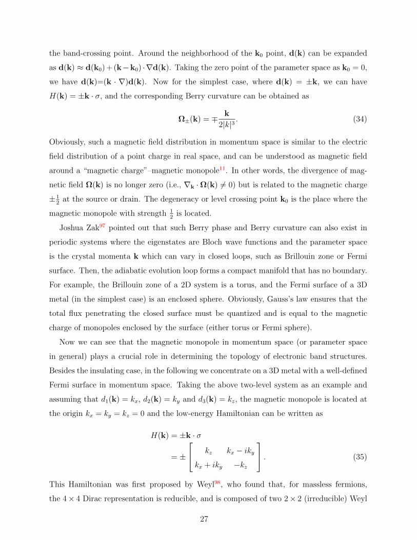
the band-crossing point. Around the neighborhood of the k0 point, d(k) can be expanded
as d(k) ≈ d(k0) + (k−k0) ·∇d(k). Taking the zero point of the parameter space as k0 = 0,
we have d(k)=(k · ∇)d(k). Now for the simplest case, where d(k) = ±k, we can have
H(k) = ±k · σ, and the corresponding Berry curvature can be obtained as
Ω±(k) = ∓ k
2|k|3. (34)
Obviously, such a magnetic field distribution in momentum space is similar to the electric
field distribution of a point charge in real space, and can be understood as magnetic field
around a “magnetic charge”–magnetic monopole11. In other words, the divergence of mag-
netic field Ω(k) is no longer zero (i.e., ∇k ·Ω(k) 6= 0) but is related to the magnetic charge
±12
at the source or drain. The degeneracy or level crossing point k0 is the place where the
magnetic monopole with strength 12
is located.
Joshua Zak97 pointed out that such Berry phase and Berry curvature can also exist in
periodic systems where the eigenstates are Bloch wave functions and the parameter space
is the crystal momenta k which can vary in closed loops, such as Brillouin zone or Fermi
surface. Then, the adiabatic evolution loop forms a compact manifold that has no boundary.
For example, the Brillouin zone of a 2D system is a torus, and the Fermi surface of a 3D
metal (in the simplest case) is an enclosed sphere. Obviously, Gauss’s law ensures that the
total flux penetrating the closed surface must be quantized and is equal to the magnetic
charge of monopoles enclosed by the surface (either torus or Fermi sphere).
Now we can see that the magnetic monopole in momentum space (or parameter space
in general) plays a crucial role in determining the topology of electronic band structures.
Besides the insulating case, in the following we concentrate on a 3D metal with a well-defined
Fermi surface in momentum space. Taking the above two-level system as an example and
assuming that d1(k) = kx, d2(k) = ky and d3(k) = kz, the magnetic monopole is located at
the origin kx = ky = kz = 0 and the low-energy Hamiltonian can be written as
H(k) = ±k · σ
= ±
kz kx − ikykx + iky −kz
. (35)
This Hamiltonian was first proposed by Weyl98, who found that, for massless fermions,
the 4× 4 Dirac representation is reducible, and is composed of two 2× 2 (irreducible) Weyl
27

fermions with positive (+) and negative (-) chirality (and opposite magnetic charge). Similar
to the definition of Chern number for a torus (in a 2D insulator), the total flux of the gauge
field passing through a Fermi surface of 3D metal must be quantized as a multiple of 2π.
We can then define the Fermi surface Chern number CFS as
CFS =1
2π
∫FS
Ω(k) · dS, (36)
and use it as a new topological invariant to describe topological metallic states. The Fermi
surface Chern number CFS is non-zero if a Weyl node (or a magnetic monopole) is enclosed by
a Fermi surface, and this leads to a non-trivial topological metallic state (called Weyl metal).
If the Fermi level happens to be exactly at the Weyl node, we will get a topological semimetal
state (i.e, Weyl semimetal). Unfortunately, according to the “no-go theorem”99,100, for any
lattice model, the Weyl nodes with opposite chirality have to appear in pairs (although they
might be separated in momentum space), and the summation of CFS for all pieces of Fermi
surfaces must be vanishing101. This makes it difficult to give a proper definition for Weyl
metal. Nevertheless, we should note that Weyl nodes (and magnetic monopoles) are stable
topological objects, which can be well defined in 3D momentum space102,103. Two Weyl
nodes with opposite signs may be separated in momentum space and lead to two pieces of
Fermi surfaces, each of which has a non-zero Fermi surface Chern number CFS 6= 0. The
two Weyl nodes may annihilate each other if and only if they overlap in k-space55,57–59,102.
Special attentions must be paid to the systems with both TRS and IS, where Kramers
degeneracy exists for every momentum k. In such cases, each pair of Weyl nodes, if any,
must overlap exactly in the k-space. In other words, the minimum effective Hamiltonian
to describe such system must be at least 4×4 and contain two Weyl nodes (with opposite
signs) simultaneously, as shown below,
H(k) =
k · σ 0
0 −k · σ
. (37)
This is called a 3D Dirac node, and is a straightforward extension of the 2D graphene
to 3D space104. As we have discussed above, in such a case, a perturbative mass term can
be introduced in principle, opening up a gap and leading to an insulating state. However,
if we consider additional symmetries in the system, such as the crystalline symmetry, the
mass term may again be forbidden, and this would stabilize the 3D Dirac cone and lead to
a 3D Dirac metal or semimetal state59,60. Therefore, the 3D Dirac node is not as stable as
28

the Weyl node, however, it is a good starting point for us to reach the true Weyl semimetal
state by breaking either TRS or IS in the 3D Dirac semimetals58.
In general, the energy level crossing may happen in many materials and at any energy
and momentum; however, it is quite rare to have band-crossing exactly at Fermi level, par-
ticularly for the cases with broken TRS or IS. Up to now, only a few materials have been
theoretically proposed to host such Weyl semimetal55–57,105 or Dirac semimetal states59,60,62.
Among them, only Na3Bi59,63 and Cd3As262,64 have been confirmed experimentally to be
Dirac semimetals. The proposed Weyl semimetals breaking TRS, such as pyrochlore Iri-
date55 and HgCr2Se456, have not been confirmed yet due to experimental difficulties. The
proposals for Weyl semimetals keeping TRS but breaking IS are thought to be a way to
overcome those difficulties. Presently the following are typical proposals: One is a super-
lattice system formed by alternately stacking normal and topological insulators106. The
second involves Tellurium, Selenium crystals or BiTeI under pressure105,107. The third one
is the solid solutions LaBi1−xSbxTe3 and LuBi1−xSbxTe3105 tuned around the topological
transition points103. The fourth is TaAs-family compounds, including TaAs, TaP, NbAs and
NbP, which are natural Weyl semimetals and each of them possesses a total of 12 pairs of
Weyl points108,109.
The Weyl semimetal is a new state of quantum matters. It is of particular interest here
that the Weyl semimetal with broken TRS is closely related to the Chern insulators and
provides a unique way to realize QAHE. Let us first consider a Weyl semimetal with a single
Weyl node in a continuous model defined as H(k) = vFk ·σ , which as mentioned previously
generates a monopole in Berry curvature right at the origin. The Gauss’s theorem then
requires that the total flux flowing through out any closed surface enclosing the Weyl point
must be ±1, i.e, equal to the chirality of the Weyl point (Eq. (36)). For a lattice system,
there is an important “no-go theorem” indicating that Weyl points must appear in pairs
with opposite chirality. Originally this theorem has been proved by field theory.99,100 Here
we provide a much intuitive way to understand it in terms of the concept of Chern number.
Given a Weyl semimetal in 3D lattice (assuming all trivial states are far away from the Fermi
level), first let’s consider a 2D plane with fixed kz, where band structures within the plane
should be fully gapped unless the plane cut through a Weyl point exactly. The integral
of Berry curvature over such a 2D insulating plane must be quantized and gives rise to a
well-defined integer Chern number. Moving the plane (i.e, kz) from -π to π, we will then get
29

the Chern number as a function of kz, as shown in Fig. 6. Now, it is important to note that
the Chern number as a function of kz should jump by +1 or -1 (depending on the chirality
of the Weyl point), whenever the moving-plane goes across a Weyl point. This is because
there exists a topological phase transition at the Weyl point, and the band gap of 2D plane
is closed and re-opened when the plane goes across the Weyl point. This jump can also be
understood by the following consideration. Selecting two planes at the opposite sides of a
Weyl point, we can construct a closed manifold surrounding the Weyl point, i.e, the cube
formed by the two parallel planes and the four side-surfaces, shown in Fig. 6 as the shaded
area. The flux flowing through the four side-surfaces should exactly cancel each other, being
net zero. Then, the total flux flowing through the closed manifold (i.e, the cube), which is
now equivalent to the difference of Chern numbers for the two parallel planes, must be equal
to the chirality of the Weyl point enclosed by the manifold (namely ±1) as discussed above.
Having understood the jump, let’s look at the Chern number evolution as the function of kz
from -π to π. In order to satisfy the periodic boundary condition in the BZ of lattice, the
positive jump (+1) and the negative jump (-1) must appear in pairs, if there is any. This
leads to the important conclusion that Weyl points with opposite chirality must appear in
pairs.
Finally, the total Hall conductivity of the system is given by the integral of kz as
σtotalxy =1
2π
∫ π
−πdkzσxy(kz). (38)
In such a way, we see the relationship between 2D Chern insulators and 3D Weyl semimetals.
Given a 3D Weyl semimetal as defined above, we can form a 2D thin film (or quantum well
structure) such that kz is quantized by the sample thickness, and only particular values of
kz are allowed. If it happens that, for some particular thicknesses, the 2D Chern number
are non-zero, we will expect quantized total Hall conductivity, and this leads to a 2D Chern
insulator and the QAHE.
To explicitly show the Hall conductivity of a FM Weyl semimetal, we introduce a simple
Hamiltonian based on a cubic lattice BHZ model110,
HWS = sin(kx)σx + sin(ky)σy + [2 + es − cos(kx)− cos(ky)− cos(kz)]σz. (39)
It has two Weyl nodes at (0,0, ±kcz) with cos(kcz)=es when 0 < es < 1. The energy dispersion
along kz axis is shown in Fig. 7 for es=12. The Hall conductivity σxy(kz) is calculated by
30

FIG. 6: Two Weyl nodes with opposite chirality (±1) distribut along kz in 3D momentum
space. The Chern number Z(kz), evaluated for each 2D plane with fixed kz, is shown at the
bottom as a function of kz. Jumps of Chern number are seen when the plane moves across
a Weyl point. A cube containing one Weyl node is shadowed.
using Eqs. (18) and (32) for each plane with fixed kz. When chemical potential µF is 0 and
passes exactly through the Weyl nodes, σxy(kz) is quantized to be 1 for |kz| < kcz and 0 for
|kz| > kcz, consistent with the above discussions based on the continuum model. Integrating
σxy(kz) over kz, the total Hall conductivity σxy is given as e2
hkczπ
111–113, which depends only on
the separation of Weyl nodes in momentum space (i.e, kcz). Shifting the chemical potential
µF away from 0 leads to partially occupied bands, and the corresponding Fermi surfaces
change from two isolated spheres (0 < µF < 0.5) to two touched ones (µF = 0.5) and finally
they merge into a peanut shape (0.5 < µF < 1.5), as shown in Fig. 7. The total Hall
conductivity decreases with rising chemical potential µF , because the Berry curvature from
the upper band tends to cancel out the contribution from the lower band. Finally, when
both bands are fully occupied the sum of Berry curvature over all bands must vanish114.
31

FIG. 7: (a) The kz band dispersion of FM Weyl semimetal. (b) The AHC dependence on
the position of chemical potential µF . Inset: Fermi surface for different µF .
It is important to note that a fully occupied band (without a corresponding Fermi surface)
may still contribute to the Hall conductivity, and this should be carefully considered in
practical calculations. In such a case, the Hall conductivity is usually evaluated by the
volume integrals of the Berry curvature of occupied bands over the whole BZ, as is done for
the calculation of intrinsic AHE11,12,35; this is also discussed by Chen et al.111 and Vanderbilt
et al.36,115–117.
32

III. FIRST-PRINCIPLES CALCULATIONS FOR TOPOLOGICAL ELECTRONIC
STATES
Theoretical predictions, particularly first-principles electronic structure calculations
based on density functional theory118, have played important roles in the exploration of
topological electronic states and materials. This is not an accidental success, but rather
due to several deep reasons: (1) To describe complicated electronic band structures of real
materials, particularly with the spin-orbit coupling (SOC) included, first-principles calcula-
tions are necessary; (2) First-principles calculations nowadays can reach the accuracy even
up to 90% for most of the physical properties of “simple” materials (i.e., weakly correlated
electronic materials), which makes prediction possible; (3) The topological electronic prop-
erties of materials are robust, non-perturbative, and not sensitive to small error bars, if any.
Given those advantages of first-principles calculations and its great success in this field,
however, we have to be aware that the numerical determination of topological invariants
(such as integer Z or Z2 numbers) is still technically demanding, because those numbers are
related to the phases of eigen wave functions, which are gauge dependent and randomized
in most of the calculations. In addition to that, we also have to note that: (1) We still
have a band-gap problem in either the local density approximation (LDA) or the general-
ized gradient approximation (GGA) for the exchange-correlation potential; (2) The present
first-principles calculations based on LDA or GGA can not treat strongly correlated systems
properly; (3) The evaluation of Berry phase27 and topological numbers may require some
additional complicities, such as fine k-points meshes, gauge-fixing condition, etc. In this
section, we will discuss some important issues and techniques related to the first principles
studies of topological electronic states.
III.A. Calculations of Berry Connection and Berry Curvature
From the computational point of view, a self-consistent first-principles electronic structure
calculation for a real material is typically performed based on the LDA or GGA for the
exchange-correlation potential. Such a calculation will generate a set of single particle eigen
states with wave functions unk(r), eigen values εn(k), and occupation fn(k) for the ground
state of the system. Having obtained those quantities, the remaining task is to evaluate the
33

Berry connection An(k) = i〈unk|∇k|unk〉 and the Berry curvature Ωn(k) = ∇k × An(k).
The Hall conductivity can be obtained either from the summation of Berry curvature over
the BZ (Eq. (16)) or from the Kubo formula directly (Eq. (17)). In the latter case, the
matrix element of velocity operator v is given as
〈ψmk|v|ψnk〉 =1
~〈umk|[
∂
∂k, Hk]|unk〉 =
1
~(En(k)− Em(k))〈umk|
∂
∂k|unk〉. (40)
The strategy is simple, but the computational task is hard, because although the Berry
curvature does not depend on the gauge choice, the Berry connection does. It is also true, ac-
cording to our above discussions, that choosing a smooth gauge for a topologically non-trivial
state is generally difficult or even impossible. In most calculations, the Berry connection is
a rapidly varying function of momentum k, which makes the convergence of the calculation
difficult. To overcome this problem, a straightforward way is to increase the number of
k-points in momentum space. Another possible way is to use the Wannier representation,
such as the maximally localized Wannier functions119.
The first-principles calculations of Berry curvature and its integration over the BZ to
get the intrinsic anomalous Hall conductivity (AHC) have been performed for SrRuO3 and
body-centered cubic Fe by Fang et al.11 and Yao et al.12, respectively. These were the
first quantitative demonstrations of strong and rapid variation of Berry curvature over the
BZ. The sharp peaks and valleys make the calculation of AHC challenging. Millions of k
sampling points are required to ensure convergence. Wang et al.35 proposed an efficient
approach employing the Wannier interpolation technique. They first perform the normal
ab initio self-consistent calculation by using relatively coarse k-grid — good enough to ensure
the total energy convergence. Then, Maximally Localized Wannier Functions (MLWF) are
constructed for the states around the Fermi level. The number of Wannier functions should
be carefully chosen so that the isolated group of bands around the Fermi level can be well
reproduced, especially those bands passing through the Fermi level (because the small energy
splitting due to spin-orbit coupling or band anti-crossing can produce sharp peaks or valleys
of Berry curvature). Once MLWFs are obtained, the interpolation technique is applied to
obtain the necessary quantities, such as eigen energies, eigen states, and velocity operator, on
a much finer k-grid. Since the number of MLWFs is typically much smaller than the number
of basis functions used in ab initio calculations, this approach saves a lot of computation
cost, both in time and in storage.
34

In additional to the direct methods discussed above, some advanced techniques with well-
controlled convergency with respect to the random phases can be developed. This is because
Berry connection is not the physical quantity that we can measure, and our ultimate goal is
to evaluate the Berry curvature which is gauge-invariant. For example, it was proposed that
for calculation of electrical polarization within the modern theory of polarization33,34 the
change of polarization is directly proportional to the sum of Berry phase terms of occupied
states. Since Berry phase is the integral of the Berry connection along a closed loop in the
parameter space (see Eq. (3)), it is well defined and gauge-independent. To calculate the
change of polarization along the direction of z, a series of loops (called Wilson loops120,121)
in momentum space are constructed. Each loop has fixed k⊥=(kx, ky), but is periodic along
kz. We can then discretize kz as kjz=jJGz (j=0, 1, ..., J-1), where Gz is the reciprocal lattice
vector along kz. Taking the periodic gauge un,(k⊥,kJz )= e−iGz ·run,(k⊥,k0z), the Berry phase
along each loop can be calculated by
γ(k⊥) = Im
[ln det
J−1∏j=0
〈un,(k⊥,kjz)|um,(k⊥,k
j+1z )〉
](41)
with band indices n and m for occupied states. By doing this, the random phase problem
associated with eigen wave functions can be largely eliminated, and the main computational
task is to evaluate the inner product of two neighboring wave functions along the loop.
For a metallic system, the intrinsic AHC can also be calculated through this method,
as has been implemented by Wang et al.36. It was justified by Haldane 117 that the non-
quantized part of intrinsic AHC in a FM metal can be recast as a Fermi surface integration of
the Berry curvature, so we can construct the Wilson loops over the Fermi surface rather than
the Brillouin zone. Considering a FM metal with magnetization M along the z direction, a
2D plane (in momentum space) perpendicular to kz will cut through the Fermi surface. The
intersection between the plane and the Fermi surface defines loops, which are the Wilson
loops used for calculating the AHC. Following our above discussions, we can discretized
each loop and evaluate the Berry phase along the loop efficiently by using Eq. (41). To do
this, several things should be borne in mind: (1) The periodic boundary condition has to be
adapted as un,(k⊥,kJz )= un,(k⊥,k0z) if the loop does not cross the Brillouin zone boundary; (2)
The direction of Wilson loops should be defined consistently; (3) For the case with multiple
branches, a continuity condition must be used to choose each branch carefully. Finally,
in additional to the non-quantized part of AHC, the quantized contribution to the AHC
35

(coming from the deep occupied states) can be determined by the Fermi-sea integration of
the Berry curvature, which is gauge invariant and has no ambiguity.
This Wilson loop method is a convenient tool, and it can also be applied to investigate
the topological invariant for systems with or without TRS as will be discussed below.
III.B. Wilson Loop Method for Evaluation of Topological Invariants
In real materials, the band structures are usually very complicated, and the determina-
tion of topological invariants becomes essential and computationally demanding. The band
degeneracy, either accidentally or due to symmetry, makes the numerical determination of
phases of wave functions a tough task. Here we will present the Wilson loop method for
determining topological indices efficiently 85,92,122,123. This method is computationally easy
and is equally applicable for Chern insulators, Z2 topological insulators (2D and 3D), and
the topological crystalline insulators124,125, which have attracted lots of interest recently.
For band insulators with inversion symmetry, the Z2 indices can easily be computed as the
product of parity eigen values for half of the occupied states (Kramers pairs have identical
parities) at the time-reversal-invariant-momentum (TRIM) points126. In such a case, parity
is a good quantum number for the TRIM points and can be computed from the eigen
wave functions obtained from the first-principles calculations. This method has been used
frequently and is very efficient. Unfortunately, for general cases where inversion symmetry
is absent, the evaluation of the Z2 number becomes difficult. Three different methods have
been considered for such a case: (i) Directly compute the Z2 numbers from the integration
of the Berry curvature Ω(k) over half of the Brillouin zone127. In order to do so, one has
to set up a fine mesh in the k-space and calculate the corresponding quantity for each k
point. Since the calculation involves the Berry connection A(k), one has to numerically fix
the gauge on the half BZ, which is not easy for the realistic wave functions obtained by
first-principles calculations. (ii) Start from an artificial system with inversion symmetry,
and then adiabatically deform the Hamiltonian towards the realistic one. If the energy gap
never closes at any point in the BZ during the deformation process, the realistic system
must share the same topological nature with the initial reference system, whose Z2 number
can easily be counted by the parity eigenvalue formula126. Unfortunately, making sure that
the energy gap remains open on the whole BZ is very difficult numerically, especially in 3D.
36

(iii) Calculate the boundary (edge or surface) states. Due to the open boundary condition,
the first-principles calculation for the boundary states is numerically heavy. The Wilson
loop method, which we will present here, has the following advantages: firstly, it uses only
the periodic bulk system; second, it does not require a gauge-fixing condition – thereby
greatly simplifying the calculation; third, it can easily be applied to a general system with
or without inversion symmetry.
As discussed in the previous section for 2D insulators, to determine the topological num-
ber (either Z or Z2), the key is the θ(ky) angle and its 1D evolution. In the single band
model, the θ(ky) angle is given simply as the 1D integration of Ax(kx, ky) along the kx axis.
However, for real compounds with multiple bands, its computation requires the Wilson loop
method92. Once the θ angle is computed, all the topological numbers can be determined
easily, following our previous discussions. For the mathematic details of this method, please
refer to our paper92. Here we will focus on the practical steps for real calculations.
Considering an insulator with N occupied states, after the self-consistent electronic struc-
ture calculations, we get the converged charge density, the total energy, the band struc-
ture, etc. Then, without loss of generality, we consider a periodic plane of (kx, ky) with
−π < kx < π and −π < ky < π, and consider the kx axis as a closed loop. For each fixed
ky, we discretize the kx line into an Nk mesh with mesh-index i ranging from 0 to Nk − 1.
Due to the periodic condition, the i=Nk point is equivalent to the i=0 point. The Wilson
loop method consists of the following steps:
(1) We need to calculate the eigen wave functions of occupied states for all mesh points.
This can be done by continuing from the converged charge density and with no need for
charge self-consistency furthermore.
(2) Using the obtained wave functions, we can calculate the inner products among them
and evaluate the N × N matrix Fm,ni,i+1 = 〈m, kx,i, ky|n, kx,i+1, ky〉, where m and n are band
indices of occupied states ranging from 1 to N . The F matrix92 is nothing but the discretized
version of Berry connection Ax.
(3) Now we can construct theN×N matrixD as the product of F , D(ky) = F0,1F1,2...FNk−2,Nk−1FNk−1,0.
(4) Diagonalization of the D(ky) matrix gives us N eigenvalues λn(ky), whose phase angle
can be obtained as θn(ky)=Im[logλn(ky)].
This phase angle θn(ky), which is now band dependent, is exactly what we need to
determine the winding number and the corresponding topological numbers, as discussed in
37

-0.5
0
0.5
-0.5 -0.25 0
θ(2π
)
ky(2π)
(e) kz=0
-0.5
0
0.5
-0.5 -0.25 0
θ(2π
)
ky(2π)
(f) kz=π
-0.5
0
0.5
-0.5 -0.25 0
θ(2π
)
(c) ky=0
-0.5
0
0.5
-0.5 -0.25 0
θ(2π
)
(d) ky=π
-0.5
0
0.5
-0.5 -0.25 0
θ(2π
)
(a) kx=0
-0.5
0
0.5
-0.5 -0.25 0
θ(2π
)
(b) kx=π
FIG. 8: (Color online) Example of Wilson loop method for the 3D strong topological
insulator TlN with Z2 index (1;000). The calculated θm(ky) for all occupied bands (m is
the band index) are plotted as functions of ky. The dashed lines are arbitrary reference
lines. The θm(ky) crosses the reference line an odd number of times in half of ky direction
(ky ∈ [0,π] or [π, 2π]) for (a) kx = 0, (c) ky = 0 and (e) kz = 0 plane (left panel), but an
even number of times for (b) kx = π, (d) ky = π and (f) kz = π plane (right panel).
Figures from Ref. 128.
section II. In practice, for a system with many bands, we can draw an arbitrary reference line
on the cylinder surface, parallel to the ky axis, and then count how many times the evolution
lines of θn(ky) cross the reference line92. For the calculation of Z2 in time-reversal invariant
systems, we can further reduce the computational task by considering only the 0 < ky < π
part. As an example, we show in Fig. 8 the calculated θn and their evolutions for one 3D
38

topological insulators TlN proposed recently128. All the six planes, each of them passing
through four TRIM points, are shown. We see that the θn lines cross the reference line an
odd number of times for all three planes containing Γ, but an even number of times for those
planes containing (π,π,π). Therefore, we conclude that it is topologically non-trivial with
Z2 index (1;000).
Finally, through the whole calculation process, we can always take advantage of Wannier
functions, particularly the maximally localized Wannier functions (MLWF) as proposed by
Vanderbilt119,129. For example, after the self-consistent electronic structure calculations, we
can construct the MLWF for the energy bands close to the Fermi level, which can usually
be reproduced up to a very high accuracy. In this process, however, some of the unoccupied
bands should be included129. Once the MLWF are obtained, we can easily calculate the
eigen wave functions and their inner products for any k-points using the interpolation tech-
nique35,130. This will greatly simplify our task for the computation of topological numbers.
In addition, the MLWF are also useful for the calculations of boundary states, as discussed
below.
III.C. Boundary States Calculations
After the determination of bulk topological numbers by either of the methods presented
above, the calculation of boundary states of real compounds becomes necessary. This is not
just for the purpose of confirming topological properties – it is also very useful for experi-
ments, such as angle-resolved photo-emission spectroscopy (ARPES) and scanning tunneling
microscope (STM), because it provides necessary information for direct comparison.
In practice, two methods are usually used for the calculation of boundary states. First,
the boundary states can be directly calculated from first-principles calculations by using a
supercell of slab geometry, as is usually done for other surface or edge calculations131. In
this way, the atomic details, such as the surface or edge terminations, the atomic relaxations
or reconstructions, the possible defects or absorptions, can be carefully treated and studied.
This method is straightforward, although it is computationally demanding. Due to the
presence of boundary states, we have to use a very large supercell with a thick vacuum
region to avoid possible mutual coupling between the boundaries. The convergence test
as a function of cell size is usually necessary. This method can generate detailed surface
39

eigen states, on the basis of which the spin texture of topological surface states (showing
characteristic spin-momentum locking effect) can be obtained. With spin-orbit coupling
included, the eigen states are expressed as two-component spinors, ψnk =
φnk↑
φnk↓
, and
the expectation value of the spin operator S = ~2σ can be calculated easily by ψ†nkSψnk
104,128.
In addition, the layer-dependent distribution of surface states (i.e, the penetration depth)
can also be studied carefully through these eigen states104.
Second, we can take advantage of MLWF and calculate the boundary states from the
Green’s functions of a semi-infinite system132. We can use the MLWF as a basis to con-
struct an effective low-energy Hamiltonian HWF , which can be regarded as a tight-binding
model with its hopping parameters determined from the first-principles electronic structure
calculations. The maximally localized property of MLWF guarantees the short range hop-
ping. Using this HWF as building blocks, we can construct a large Hamiltonian Hsemi for
the semi-infinite system with only one boundary. This Hsemi is a block tridiagonal matrix
if we consider only the hopping terms between the nearest-neighbor building blocks. In
practice, we find that the thickness of the building block should also be tested to ensure
convergence since in some cases the hopping among MLWFs might extend to more than
the nearest-neighbor. Then we can use the iterative method133–135 to solve the problem
and get the projected Green’s functions onto the boundary. From these boundary Green’s
functions, we can get necessary information such as the charge density of states and the spin
density of states at the boundary136,137. This procedure is an approximate way and it cannot
treat the atomic details at the boundary precisely, however, it provides the most important
information for the gapless nature of the boundary states of topological insulators.
IV. MATERIAL PREDICTIONS AND REALIZATIONS OF QAHE
The topological electronic states discussed in previous sections are important and inter-
esting, not only because they are conceptually new but also because they are realizable and
testable in condensed materials. In recent years, this field has been developing very fast.
Many candidate compounds with non-trivial topological electronic states are proposed, and
some of them have been successfully synthesized and confirmed experimentally. The re-
alizations of various topological electronic states have strongly promoted this field, and a
40
lot of interesting experiments on their non-trivial topological properties are now becoming
possible. In this section we will focus on the topic of how to realize the QAHE in real
materials.
In spite of great success in recent studies of TIs and QSHE, the realization of QAHE
has taken a long time. The key to achieving this goal is to find a proper Chern insulator.
Any realistic material system in which QAHE can be realized must satisfy the following
conditions:
1. It must be two dimensional;
2. It must be insulating in the bulk;
3. It must break the TRS with a certain magnetic ordering (the simplest case is a FM
long-range order);
4. The occupied bands must carry a non-zero Chern number (therefore strong SOC is
usually required).
It is not difficult for a material to satisfy one or two conditions in the above list. But
finding a realistic material that satisfies all of these conditions simultaneously turns out
to be very challenging. This is the reason the Chern insulator is theoretically proposed
long before the discovery of TIs, but its realization came much later. Nevertheless, the
discovery of QSHE and TIs38,39,41,43,49,50,93 have greatly stimulated the field of QAHE. It is
natural to expect that starting from known 2D TIs and then breaking the TRS will be one
of the simple ways to achieve the QAHE. The 2D TIs already satisfy three out of those four
conditions, and these TIs can be effectively viewed as two Chern insulator layers related
by TRS. Breaking of TRS can, in principle, destroy one layer and keep the other layer
active, which will lead to the QAHE. Based on this idea, we can go further: if the exchange-
splitting is strong enough, we can even realize the QAHE starting from a 2D narrow gap
semiconductor, where the strong exchange-splitting may cause band inversion for half of the
states (i.e, for only one of the spin subspaces, as will be addressed below). Unfortunately, it
is still very hard to induce exchange-splitting in 2D TIs or narrow gap semiconductors; two
known procedures, the magnetic proximity effect and magnetic doping, are most commonly
employed. Despite the issue of magnetic ordering temperature Tc (which can be very low),
magnetic doping will obviously introduce impurities that may destroy the insulating state
41

of parent compounds. On the other hand, using the magnetic proximity effect may have the
advantage of avoiding the problem of impurity doping, while the possible exchange-splitting
induced by this procedure is typically very weak. Therefore, in practice, we have to choose
the candidate compounds and procedures carefully in order to balance various conditions
and requirements. In this sense, the first-principles calculations play important, predictive
roles for the final realization of the QAHE. As listed below, up to now, there have been
several different types of proposals for the realization of the QAHE, and most of them start
from TIs as the parent compounds.
• To sandwich a TI thin film with FM insulators. The FM proximity effect will open
up a gap for the Dirac surface states on both surfaces of the TI, which gives rise to
the QAHE74.
• To dope the magnetic ions into the TI thin film and make it a FM semiconductor138–140.
The QAHE can be obtained by proper control of the doping. This is the only one of
these proposals that has succeeded so far141,142.
• To make a thin film (or quantum well structure) of a FM Weyl semimetal (such
as HgCr2Se4). The quantum size effect gives rise to the quantization of the crystal
momentum along the growing axis, which at the same time quantizes the anomalous
Hall coefficient at a certain film thickness56,143.
• To grow graphene, silicene, or other honeycomb lattice on top of magnetic insulators
or with magnetic adsorbates. The low energy bands (which are tunable by external
electric field) acquire both the Zeeman exchange-splitting and the SOC, which drive
the system towards QAHE144–155.
• To mimic the honeycomb lattice by growing double-layer thin films of a transition
metal oxide with perovskite structure along the (111) direction, or by forming a sheet
of organic moleculars that contain transition-metal ions. The magnetic long-range
order might be stabilized among the d electrons of the transition metal. The QAHE
can be realized in such systems if a suitable exchange field is established156–163.
• Other proposals, such as heavy metal on magnetic insulator substrate164, strained
epitaxial film with interface band inversion in EuO/GdN165 or CdO/EuO166, etc.
42

FIG. 9: (Color online) Illustration of the band inversion mechanism. Schematic plot for
the band structure with normal order (m<0), inverted order (m>0) without SOC, and
inverted order with SOC, respectively. (See main text for detailed explanations).
Most of the proposals mentioned above are supported by first-principles calculations,
and we will start this section with a brief introduction about how to explore new topological
materials from the viewpoint of a band inversion mechanism. Then we will discuss details of
some of the proposals for the prediction and realization of the QAHE, with no attempting
to cover them all.
IV.A. Band Inversion Mechanism
Though we have found, in the previous sections, that the Wilson loop method can reduce
computation effort in calculating various topological invariants, it is still quite tedious and
inefficient for wide-range searching or design of topological materials. From this point of
view, band inversion is the most intuitive picture and most practically useful guideline for
the initial screening of possible topological materials. Band inversion involves the energy
order switching of low energy electronic bands around a certain TRIM point in the Brillouin
Zone when compared with the energy ordering in the atomic limit (which is topologically
trivial). Band inversion may happen when atoms form crystalline solids and acquire strong
enough band dispersions. The mechanism was first demonstrated for a HgTe/CdTe quantum
well structure41 and later was found to be applicable to many other materials, including 2D
and 3D TIs43,53,167–169, Chern insulators139, topological Weyl semimetals55,56 and topological
Dirac semimetals59,62.
43

As schematically illustrated in Fig. 9, we consider two bands close to the Fermi level
around the Γ point. Far away from the Γ point, the red state is occupied and energetically
lower than the blue state. However, close to Γ point, they have an inverted energy ordering
with the blue state lower and occupied at Γ. Let us assume that two bands do not couple
when the SOC is absent, and they must cross at certain k-point away from the Γ point. For
time-reversal-invariant systems with SOC, the spin degree of freedom has to be taken into
account, and at least four bands must be included in this simple model. The band crossing
points are, in general, not stable and will open up a gap (in the presence of SOC). As a
result, the system becomes an insulator if the chemical potential is located within the gap,
and most importantly, this gapped state may be topologically non-trivial depending on the
coupling terms. It should be noted that if additional crystal symmetries are considered, the
four-fold degenerated band crossings are possibly protected. This situation is demonstrated
in topological Dirac semimetals59,62.
To be more explicit, we consider two parabolic bands with energy dispersion E±(k) =
±(−m + k2). The + and − signs are for the blue and red bands, respectively. The band
inversion (around k=0) happens for the parameter region of m > 0. We first focus on a 2D
system with broken TRS. Using two bands as a basis, we can construct an effective 2×2
Hamiltonian,
Heff (k) =
E+(k) M(k)∗
M(k) E−(k)
, (42)
whereM(k) is the coupling between the two bands that determines the topological properties
of the resulting electronic structure. If m < 0, i.e., without band inversion, we will in general
expect nothing but a normal insulator. However, if m > 0 for the band-inverted system,
we may find many interesting topological phases, depending on the choice of M(k). For
example, if M(k) = (kx ± iky)n (n ≥ 1), we will get a Chern insulator with Chern number
Z = n (for a 2D system). For a 2D system with TRS, the two bands should be replaced
by four bands with each color (blue and red) representing a Kramers pair of bands, and
the model Hamiltonian becomes 4×4 (block diagonal in its simplest form, such as the BHZ
Hamiltonian41). If we now have a form of M(k) = (kx ± iky)2n−1, we will expect a 2D
topological insulator with Z2=1. In the presence of SOC, these forms of coupling term
M(k) are in general allowed, and they depend on the material’s details. Similar discussions
can be extended to 3D systems, and in this case, we can expect either 3D TIs170 or 3D
44

topological semimetals56,59,62. In real compounds, the band inversion may happen between
s-p, p-p, p-d, or d-f states, which leads to different material classes of TIs167.
The band inversion mechanism discussed above is practically useful, yet a crude picture
for real compounds. First, this picture comes from the low energy effective Hamiltonian of a
continuous model. If we put the model onto a lattice, we have to be careful about the number
of times band inversion occurs. Particularly for the Z2 TIs, if band inversion happens an
even number of times or it happens around an even number of TRIM points, we will return
to a trivial insulator phase (in the sense of Z2=0, although other topological phases, such as
topological crystalline insulator124,125, may be defined). Second, real compounds may have
many low energy bands that are strongly fixed and must be carefully analyzed. Third, the
possible M(k) terms can also be complicated and need to be treated carefully. In any case,
a final conclusion must be carefully made based first-principles calculations as presented in
previous sections.
IV.B. QAHE in Magnetic Topological Insulators
Several realistic systems, including Mn doped HgTe quantum wells138, magnetic-impurity
doped Bi2Se3 thin films139, Mn doped InAs/GaSb quantum wells140, magnetically doped
junction Quantum Wells171, etc, have been proposed to support the QAHE. The essence of
these proposals is to break the TRS in a 2D slab of QSHI by magnetic doping. If the FM
order can be established, the introduced exchange splitting may destroy the band inversion
in half of the states (say, for one spin channel), while keeping the band inversion in the other
half of the states, leading to the QAHE.
A HgTe quantum well with an appropriate thickness realized between two CdTe barriers
can achieve the 2D QSH state41,42. Based on this structure, Liu et al. proposed that the
QAHE can be obtained by magnetic Mn-doping in HgTe/CdTe quantum wells138, if the
doped Mn ions are ferromagnetically ordered with magnetic momentum polarized along
the out-of-plane direction. Unfortunately, (Hg1−xMnx)Te is experimentally paramagnetic
(rather than FM), which prohibits the realization of QAHE. Due to the paramagnetic nature,
in practical measurement, a magnetic field is required to polarize the Mn magnetic moment.
Therefore, it is hard to distinguish the Hall and the anomalous Hall contributions. With
the same idea, Zhang et al. 171 proposed that a QSHI with bulk band gap around 0.1 eV
45

can be realized in junction quantum wells comprising II-VI, III-V, or IV semiconductors,
and proper magnetic ordering can drive the system into the QAH state. Experimentally
again, we have to wait for the synthesis and the well-controlled doping of a sample. In the
following, we will take Bi2Se3 and Bi2Te3 (well-known topological insulators), as paradigms
to show how the QAHE state is achieved in their thin film form with Cr-doping. This is the
only experimentally successful example so far141.
FIG. 10: (Color online) Crystal structure of the Bi2Se3 family of compounds. (a) The
hexagonal supercell containing 15 atomic layers. (b) Top view of a QL in the triangular
lattice. Three sets of different sites, labeled as A, B and C sub-lattices, respectively, are
presented. (c) The first BZ. Four non-equivalent TRIM points Γ (0, 0, 0), L(π,0,0),
F (π,π,0) and Z(π,π,π) are denoted in the 3D BZ. The corresponding surface 2D BZ is
represented by the dashed hexagon, and Γ, M and K are the corresponding TRIM special
k points in the surface BZ. Figure from Ref. 104.
The Bi2Se3 family of compounds have a rhombohedral crystal structure with space group
D53d (R3m). The system has a layered structure with five atomic layers as a basic unit, named
46

a quintuple layer (QL), as shown in Fig. 10. The materials Bi2Se3, Bi2Te3 and Sb2Te3 have
been theoretically predicted and experimentally observed to be topological insulators with
a large bulk band gap43–52. Recent experimental progress has shown that well-controlled
layer-by-layer MBE thin film growth can be achieved45,172, and various magnetic transition
metal elements (such as Ti, V, Cr, Fe) can be substituted into the Bi2Se3 family of parent
compounds with observable ferromagnetism even above 100K173–177.
We first discuss how to achieve a FM insulating phase in a semiconductor doped with
dilute magnetic ions. To simplify the discussion, we divide the whole system into two sub-
systems describing the local moments and the other band electrons, respectively. We further
assume that the magnetic exchange among local moments is mediated by the band electrons.
If we consider only the spatially homogeneous phase, the total free energy of the system in
an external magnetic field H can be written as
Ftotal =1
2χ−1L M2
L +1
2χ−1e M2
e − JeffMLMe − (ML +Me)H, (43)
where χL/e is the spin susceptibility of the local moments/electrons, ML/e denotes the mag-
netization for the local moment and electron sub-system and Jeff is the magnetic exchange
coupling between them. The spontaneous FM phase can be realized when the minimization
procedure of the free energy gives a non-zero magnetization in the zero magnetic field limit
(H=0). This leads to the requirement of J2eff−χ−1L χ−1e > 0, or equivalently χe > 1/(J2
effχL).
This result means that in order to have a non-zero FM transition temperature (Tc), a sizable
χe is needed. Within linear response theory, the spin susceptibility χe for a insulator is given
by the van Vleck formula
χzze =∑v,c,k
4µ0µ2B
〈vk| Sz |ck〉 〈ck| Sz |vk〉Eck − Evk
, (44)
where µ0 is the vacuum permeability, µB is the Bohr magneton, |ck〉 and |vk〉 are the
Bloch functions in the conduction and valence bands respectively, Eck and Evk are the eigen
energies of |ck〉 and |vk〉, and Sz is the spin operator of electrons and we consider only the
z-direction, i.e. perpendicular to the 2D plane, for simplicity.
In most dilute magnetic semiconductors, such as (Ga1−xMnx)As, which has s-like conduc-
tion and p-like valence bands, the matrix elements 〈ck| Sz |vk〉 are very small. The electronic
spin susceptibility is therefore negligible for the insulating phase, and a finite carrier density
is required to mediate the magnetic coupling (for example, by the RKKY mechanism178).
47

0
0.25
0.5
0.75
1
1.25
1.5
1.75
0 0.25 0.5 0.75 1 1.25
χ (
10
-9 m
3/m
ol)
λ/λ0
FIG. 11: Van-Vleck type spin susceptibility of Bi2Se3 bulk as a function of spin-orbit
coupling (SOC) strength (λ0 is the actual SOC strength). Figure from Ref. 139.
For the Bi2Se3 family of materials, however, the semiconductor gap is opened by the SOC
between two p-orbital bands. The spin operator Sz has finite matrix elements between the
valence and conduction bands, which are further enhanced due to the band inversion139.
In Fig. 11, we show the calculated spin susceptibility of bulk Bi2Se3. At the Γ point, the
band inversion occurs when the relative SOC strength λ/λ0 exceeds 0.5, and after that the
spin susceptibility starts to increase rapidly. At the actual SOC strength, Bi2Se3-family
materials have a considerable spin susceptibility χzze . Hence the local moments of the mag-
netic impurities in such materials can be ferromagnetically coupled through the van Vleck
mechanism179. Recently the interplay between magnetism and the topological property in a
material has been discussed in more details in Ref. 180 and 181.
From first-principles calculations, we find that the insulating magnetic ground state dis-
cussed above can indeed be obtained by a proper choice of magnetic dopants. Experiments173–175
and theoretical calculations139,182 show that the magnetic dopants will mostly substitute for
Bi ions, which has a nominal 3+ valence state. In order to avoid introducing free carriers
into the parent material when we dope the system, it is natural to choose those transition
metal elements that also have a stable 3+ chemical state, such as Ti, V, Cr and Fe. Self-
consistent first-principles calculations for Bi2Se3 doped with Ti, V, Cr and Fe have been
performed. The calculated densities of states (DOS) shown in Fig. 12 suggest that an
48

-40
-20
0
20
40
-4 -3 -2 -1 0 1
DO
S (
sta
tes/e
V)
Energy (eV)
(A) Ti total3d
-40
-20
0
20
40
-4 -3 -2 -1 0 1
DO
S (
sta
tes/e
V)
Energy (eV)
(B) V total3d
-40
-20
0
20
40
-4 -3 -2 -1 0 1
DO
S (
sta
tes/e
V)
Energy (eV)
(C) Cr total3d
-40
-20
0
20
40
-4 -3 -2 -1 0 1
DO
S (
sta
tes/e
V)
Energy (eV)
(D) Fe total3d
FIG. 12: Calculated densities of states (DOS) for Bi2Se3 doped with different transition
metal elements. The Fermi level is located at energy zero, and the positive and negative
values of DOS are used for up and down spin, respectively. The lines are projected partial
DOS of the 3d states of transition metal ions. It is shown that Cr or Fe doping will give
rise to the insulating magnetic state. Figure from Ref. 139.
insulating magnetic state is obtained only for Cr or Fe doping, while the states are metallic
for Ti or V doping cases.
The above results can be understood as illustrated in Fig. 13. We first point out that,
for all the cases, the dopants are nearly in the 3+ valence state, and we always obtain
the high-spin state due to the large Hund’s coupling of 3d transition metal ions. For the
Fe-doped case, the Fe3+ favors the d5↑d0↓ configuration in a high-spin state, resulting in a
gap between the majority and minority spins, which directly leads to the insulating state
in Fe-doped samples as shown in Fig. 13a. For the Cr-doped case, Cr ions substitute in
the Bi sites and feel an octahedral crystal field formed by the six nearest neighboring Se2−
ions. Such a local crystal field splits the d-shell into t2g and eg manifolds. This splitting
49

is large enough to stabilize the t3↑2ge0↑g t
0↓2ge
0↓g configuration of a Cr3+ ion, resulting in a gap
between the t2g and eg manifolds, as shown in Fig. 13(b). For the case of Ti or V doping,
the t2g manifold is partially occupied, leading to the metallic state, as shown in Fig. 13(c).
We note that, although the local density approximation in density functional theory may
underestimate the electron correlation effects, the inclusion of electron-electron interaction
U (such as in the LDA+U method) should further enhance the gap (it may also reduce the
p-d hybridization and Tc183).
The exchange field ∆ can be estimated as ∆ = xJeff〈S〉 at the mean field level, where
x is the doping concentration and 〈S〉 is the mean field expectation value of the local spin,
Jeff is the effective exchange coupling between the local moments and the band electrons,
which is estimated to be around 2.7 eV for Cr-doping and 2.8 eV for Fe-doping in Bi2Se3
by first-principles calculations. With the concentration of the magnetic dopants at 10%, the
FM Curie temperature can be estimated in the mean field approximation184 to reach the
order of tens of K.
Once the FM order is achieved in TI at a reasonable temperature, the QAHE can in
principle be realized in 2D thin films of such systems by tuning the exchange splitting (i.e,
the density of magnetic doping). Since the bulk states are always gapped, we focus on the
simplest low energy effective Hamiltonian consisting of Dirac-type surface states only:
H = Hsf +HZeeman
=
−vF (k × σ)z m∗k
mk vF (k × σ)z
+
gMσz 0
0 gMσz
, (45)
with the basis of |t ↑〉 , |t ↓〉 , |b ↑〉 , |b ↓〉, where “t” (“b”) represents the surface states on the
FIG. 13: The configuration of the d electrons for the (a) Fe, (b) Cr, (c) Ti and V doping
cases.
50

FIG. 14: Evolution of the subbands structure upon increasing the exchange field. The red
color denotes the subbands that have even parity at the Γ point, and blue color denotes
subbands with odd parity at the Γ point. The dashed lines denote the spin up electrons;
solid lines, spin down electrons. (a) The initial subbands are not inverted. When the
exchange field is strong enough, a pair of inverted subbands appears (red solid line and
blue dashed line). (b) The initial subbands are already inverted. The exchange field
releases the band inversion in one pair of subbands (red dashed line and blue solid line)
and increases the band inversion in the other pair (red solid line and blue dashed line).
top (bottom) surface, and “↑”, “↓” represent the spin up and down states, respectively. vF
is the Fermi velocity, mk describes the tunneling effect between the top and bottom surface
states, g is the effective g-factor, σ are the Pauli matrices, and M represents the exchange
field along the z-direction, introduced by the FM ordering. For simplicity, spatial inversion
symmetry is assumed, which requires that vF , g and M take the same values for top and
bottom surfaces. In thick enough slab geometry (mk ≈ 0), the spatially separated pairs of
surface states are well defined for the top and bottom surfaces. However, with the reduction
of the film thickness, quantum tunneling between the top and bottom surfaces becomes
more and more pronounced, giving rise to a finite mass term mk, which can be expanded
as mk = m0 + B(k2x + k2y) up to the second order of k. The Hamiltonian can be rewritten
51

in terms of the symmetric and anti-symmetric combination of the surface states on top and
bottom surfaces as
H = Hsf + HZeeman =
hk + gMσz 0
0 h∗k − gMσz
, (46)
with the following new basis: |+ ↑〉, |− ↓〉, |+ ↓〉, |− ↑〉, where |± ↑〉 = (|t ↑〉 ± |b ↑〉)/√
2,
|± ↓〉 = (|t ↓〉 ± |b ↓〉) /√
2. Here h(k) = mkσz + vF (kyσx − kxσy), which is similar to the
BHZ model describing the low energy physics in HgTe/CdTe quantum wells41. When m0B <
0, band inversion occurs, and the system will be in the QSH phase if this is the only band
inversion between two subbands with opposite parity. Regardless of whether this condition
is satisfied or not, a strong enough exchange field will induce the QAH effect in this system,
thanks to the presence of the σz matrix in the exchange field (gMσz) and the opposite signs
of the Zeeman coupling terms in the upper and lower blocks of the effective Hamiltonian
in Eq. (46). The exchange field breaks the TRS and increases the mass term of the upper
block, while reducing the mass term for the lower block. More importantly, a sufficiently
large exchange field can change the Chern number of one of the two blocks. There are
two cases, as illustrated in Fig. 14. In the first case, the four-band system is originally in
the topologically trivial phase; the exchange field will induce band inversion in the lower
block and push the two sub-bands in the upper block even farther away from each other.
Therefore, the 2D model with a negative mass in the lower block contributes −e2/h for
the Hall conductance (see Fig. 14(a)). In the other case, the system is originally in the
topologically non-trivial phase, and both blocks have inverted band structures. A sufficiently
large exchange field can increase the band inversion in the lower block and release the band
inversion in the upper block. Again the negative mass in the lower block contributes −e2/h
for the Hall conductance (see Fig. 14(b)). Such a mechanism is general for the thin films of
TIs with FM ordering, it is guaranteed by the fact that the surface states on the top and
bottom surfaces have the same g-factor.
In Fig. 15 A-C, we plot the lowest four sub-band levels at the Γ point as functions of
exchange field. Level crossings between the lowest conduction bands (blue lines) and valence
bands (red lines) are found for all three values of layer thickness, signaling the quantum phase
transition to the QAH state. In the insulator case, where the chemical potential is located
inside the energy gap between the conduction and valence sub-bands, the Hall conductance
is determined by the Chern number of the occupied bands and must be an exact integer
52

-0.15
-0.1
-0.05
0
0.05
0.1
0.15
-0.5-0.4-0.3-0.2-0.1 0
En
erg
y (
eV
)
Exchange field (eV)
(A)
Ma
-0.1
-0.05
0
0.05
0.1
-0.4-0.3-0.2-0.1 0
En
erg
y (
eV
)
Exchange field (eV)
(B)
Mb
-0.02
-0.01
0
0.01
0.02
-0.08-0.06-0.04-0.02 0
En
erg
y (
eV
)
Exchange field (eV)
(c)
Mc
0
0.5
1
-0.3-0.2-0.1 0
σxy (
e2/h
)
Exchange field (eV)
(D)
3 QL
4 QL
5 QL
FIG. 15: Quantized anomalous Hall (QAH) conductance. (A), (B) and (C) are the lowest
sub-bands at the Γ point, plotted versus the exchange field, for Bi2Se3 films with
thicknesses of 3, 4 and 5 quintuple layers (QL), respectively. The red lines denote the top
occupied (bottom unoccupied) states. With an increase of the exchange field, a level
crossing occurs (indicated by arrows), indicating a quantum phase transition to QAH
state. (D) Calculated Hall conductance for 3, 4 and 5 QL Bi2Se3 films under ferromagnetic
exchange field. As we expect, the Hall conductance is zero before the QAH transition, but
σxy = e2/h afterward. Figure from Ref. 139.
multiple of e2/h. The calculated Hall conductance for Bi2Se3 thin films of three typical
thicknesses (Fig. 15 D) jumps from 0 to 1 at the corresponding critical exchange field for
the level crossing. The QAH effect with higher Hall conductance plateaus in the Cr-doped
53

-0.4
-0.2
0
0.2
0.4
K Γ M
Energ
y (e
V)
(A)
-0.1
0
0.1
0.2
0.3
0.4
-0.2 -0.1 0 0.1 0.2
σxy
(e
2/h
)
Chemical potential (eV)
(B)
-0.4
-0.2
0
0.2
0.4
K Γ M
Energ
y (e
V)
(C)
-1
-0.5
0
0.5
1
-0.2 -0.1 0 0.1 0.2
σxy
(e
2/h
)
Chemical potential (eV)
(D)
-0.4
-0.2
0
0.2
0.4
K Γ M
Energ
y (e
V)
(E)
-0.02
0
0.02
Γ
-0.1
0
0.1
0.2
0.3
0.4
-0.2 -0.1 0 0.1 0.2
σxy
(e
2/h
)
Chemical potential (eV)
(F)
-0.4
-0.2
0
0.2
0.4
K Γ M
Energ
y (e
V)
(G)
-0.02
0
0.02
Γ
0
0.2
0.4
0.6
0.8
1
-0.2 -0.1 0 0.1 0.2
σxy
(e
2/h
)
Chemical potential (eV)
(H)
FIG. 16: The sub-bands dispersion of 2D Bi2 Se3 thin film are plotted for 3QL slab with
exchange field (A) -0.05 eV, (C) -0.24 eV. The corresponding Hall conductance are plotted
in the right panels as the function of the chemical potential. The zero chemical potential
corresponds to the ideal stoichiometry case. The systems in (A) is normal insulator, which
has zero platforms in Hall conductance when the chemical potential locates in the energy
gap. The system in (C) is QAH insulators, in which the Hall conductance has quantized
value e2/h . Figure from Ref. 139.
Bi2(Se,Te)3 was further discussed in Ref. 185, where the stronger exchange field leads to
more band crossings and a larger Chern number.
In Fig. 16, we plot the sub-band dispersion and corresponding Hall conductance as
functions of chemical potential for 3 QL Bi2Se3 thin films with different exchange fields. A
quantized plateau in Hall conductance should be observed when the chemical potential is
inside the gap. For the QAH phases (Fig. 16 (D)), a non-zero integer plateau is observed
54

when the chemical potential falls into the energy gap; while for the non-QAH phases (Fig.
16 (B)), the corresponding Hall conductance is zero. In a recent experiment, Chang, et al.141
prepared the Cr-doped (Bi,Sb)2Te3 thin films with well controlled chemical potential and
long-range ferromagnetic order. Careful control of the Bi and Sb concentration is needed to
separate the surface states from the bulk states. By tuning the gate voltage (and therefore,
the chemical potential), they observed the quantization of the Hall resistance at h/e2 at zero
external magnetic filed with temperature around 30 mK, accompanied by a considerable drop
in the longitudinal resistance. A similar experiment was further performed by Checkelsky, et
al.142, confirming the existence of QAHE in this system. For readers who want to know more
experimental details, please refer to their original papers. To conclude this part, we finally
point out that the QAHE can be induced even by in-plane magnetization, as discussed in
Ref. 186.
IV.C. QAHE in thin film of Weyl semimetals
As discussed in sec. II.C, Weyl semimetal is a new topological state of 3D quantum
matter, unlike the 3D topological insulators. It can be characterized by Weyl nodes at the
Fermi level in the bulk and Fermi arcs on surfaces. Around Weyl nodes, the low-energy
physical behavior is like that of 3D two-component Weyl fermions98 and can be described
by the Hamiltonian H = vfσ ·k, where vf is the Fermi velocity, σ is the vector of the Pauli
matrices, and k is the momentum as measured from the Weyl node. A Weyl fermion is
half of a Dirac fermion, and Weyl fermions must appear in pairs. The Weyl Hamiltonian is
robust against perturbations since it uses all three of the Pauli matrices. The perturbations
only shift the position of the gap-closing point in momentum space and the Weyl nodes
can be removed only when a pair of them meet in momentum space. To obtain a Weyl
semimetal, either time-reversal symmetry or inversion symmetry must be broken, and there
have been several proposals to realize this55–57,105–109. In particular, Weyl semimetals are
closely related to the chiral anomaly187, and the QAHE can naturally be expected in the
quantum well structure of Weyl semimetals with broken TRS. In this section, based on first-
principles calculations, we will show that HgCr2Se4 is a FM Weyl semimetal with Fermi arcs
on its surface, and its 2D thin film is a promising system for realizing the QAHE.
HgCr2Se4 is a FM spinel exhibiting large coupling effects between electronic and magnetic
55

FIG. 17: (Color online) Crystal structure of HgCr2Se4 spinels.
properties188. The spinel structure (space group Fd3m) of HgCr2Se4 with Cr3+ octahedrally
surrounded by Se ions, as shown in Fig. 17, yields a half-filled t2g shell and a spin number of
S=3/2. First-principles calculations56 confirm that FM solution is considerably (2.8 eV/f.u.)
more stable than non-magnetic solution, and the calculated moment (6.0 µB/f.u.) is in good
agreement with experiments189,190. Without SOC, the electronic structures shown in Fig.
18(a) and (b) suggest that it is nearly a “zero-gap half-metal”. It is almost a half-metal
because a gap exists only in the up-spin channel just above the Fermi level; it is nearly
zero-gapped because of the band-touching around the Γ point just below Fermi level in
the down-spin channel. Quite large exchange splitting and strong octahedral crystal field
together lead to a high spin state of Cr3+ ions in a t3↑2ge0↑g t
0↓2ge
0↓g configuration with a gap
between the t3↑2g and e0↑g manifolds as schematically shown in Fig. 18(c). The Se-4p states
(located from about -6 eV to 0 eV) are almost fully occupied and contribute to the top part of
the valence band dominantly. The hybridization with Cr-3d states makes the Se-4p slightly
spin-polarized with the opposite moment (about -0.08 µB/Se). The zero-gap behavior in
the down spin channel is the most important characteristic here (Fig. 18(b)), because it
56

suggests the inverted band structure around Γ, similar to the case in HgSe or HgTe191,192.
-8 -6 -4 -2 0 2 4Energy (eV)
-16
-8
0
8
16
Den
sity
of
Sta
tes(
/eV
/u.c
.)
R Γ X M Γ-2
-1
0
1
2
Ener
gy
(eV
)
R Γ X M Γ
EF
GGA+SOC
R Γ X M Γ Z
-0.5
-0.4
-0.3
-0.2
-0.1
0
0.1
En
erg
y(e
V)
EF
1
2,1
2
1
2, -1
2
S, -1
2
− −
− −
−
Γ
-0.04
-0.02
0
0.02 3
2,3
2
3
2,1
2
3
2,1
2
3
2,3
2
B
− −
− −
− −
− −-
-
A
a
b
d
c
spin up spin down
Se PS
S
Se P
Cr ge
Cr2gt
Hg 5d
Cr2gt
Cr g
Total DOS
Hg 5d
Se 4p
Cr e
Cr tg
2g
e
EF
FIG. 18: (Color online) Electronic structures of HgCr2Se4. (a) The total and projected
partial density of states (DOS); (b) The band structures without SOC (showing the up and
down spin parts separately); (c) Schematic plot of band-inversion, where the |S, ↓〉 state is
lower than the |P 〉 states; (d) The band structure including SOC (with majority spin along
the (001) direction). The detail around Γ is enlarged in inset. Figure from Ref. 56.
Taking the four (eight if spin is considered) low energy states at the Γ point as basis,
which are identified as |Px〉, |Py〉, |Pz〉, and |S〉, the low energy physics becomes the same
as in HgSe or HgTe, and the only difference is the presence of exchange splitting. The band
inversion (see Fig. 18(c); |S, ↓〉 is lower than |P 〉) is due to the following two factors: 1)
Hg-5d states around -7.0 eV below Fermi level are very shallow and their hybridization with
Se-4p states has pushed the anti-bonding Se-4p states quite high, similar to the situation
in HgSe. 2) The hybridization between unoccupied Cr-3d↓ and Hg-6s↓ states will push the
Hg-6s↓ state to lower in energy. These two key factors lead to band inversion, with the |S, ↓〉
lower than the |P 32, 32〉 states by about 0.4 eV. This value is further enhanced to be 0.55 eV
57

kzc
k
k
k
z
x
y
C number
2
0
1
kzc - /a /a
kz
-kzc
a b
c(π
/a)
y
xk (π/a)
0.0 kd
-11 -1 -0.5 0.0 0.5 1
-1
-0.5
0.0
0.5
1
kz
(π/a
)
kx (π/a)
0.0
1
-1
-kzc
FIG. 19: (Color online) Weyl nodes and gauge flux in HgCr2Se4. (a) The band-crossing
points in ~k-space; (b) Chern number as function of kz; (c) Schematic plot of the band
dispersion around the Weyl nodes in the kz=±kcz plane, and the inset shows the chiral spin
texture. (d) Gauge flux evaluated as Berry curvature in the (kx, kz) plane. Figure from
Ref. 56.
in the presence of SOC. Further LDA+U calculations (with effective U around 3.0eV193,194)
indicate that the band-inversion remains even if the correlation effect is properly considered,
unless U is unreasonably large (> 8.0 eV). Experimental observations of metallic behavior
at low temperature for various samples195–197 strongly support this conclusion of inverted
band structure.
In the presence of SOC, the low energy eigenstates at Γ are given as |32,±3
2〉, |3
2,±1
2〉,
|12,±1
2〉, and |S,±1
2〉, which can be constructed from the |P 〉 and |S〉 states, similar to the
58
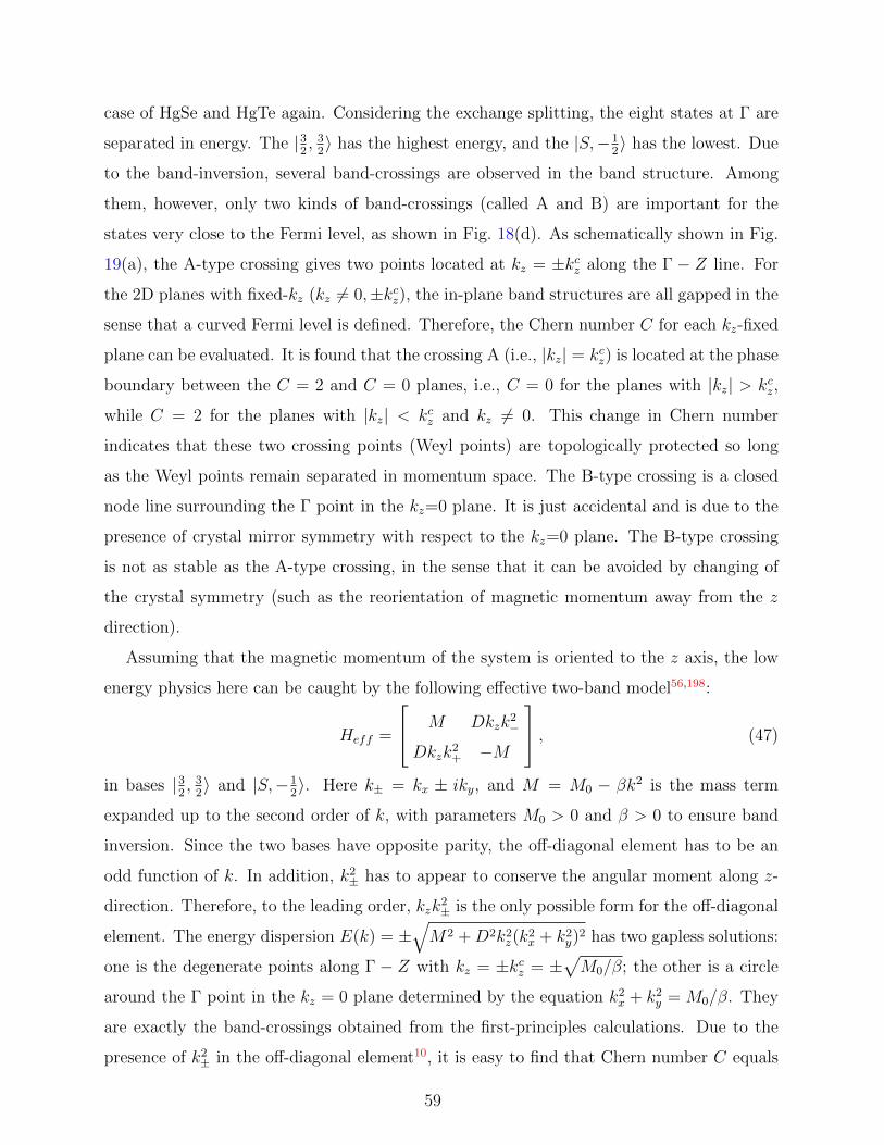
case of HgSe and HgTe again. Considering the exchange splitting, the eight states at Γ are
separated in energy. The |32, 32〉 has the highest energy, and the |S,−1
2〉 has the lowest. Due
to the band-inversion, several band-crossings are observed in the band structure. Among
them, however, only two kinds of band-crossings (called A and B) are important for the
states very close to the Fermi level, as shown in Fig. 18(d). As schematically shown in Fig.
19(a), the A-type crossing gives two points located at kz = ±kcz along the Γ − Z line. For
the 2D planes with fixed-kz (kz 6= 0,±kcz), the in-plane band structures are all gapped in the
sense that a curved Fermi level is defined. Therefore, the Chern number C for each kz-fixed
plane can be evaluated. It is found that the crossing A (i.e., |kz| = kcz) is located at the phase
boundary between the C = 2 and C = 0 planes, i.e., C = 0 for the planes with |kz| > kcz,
while C = 2 for the planes with |kz| < kcz and kz 6= 0. This change in Chern number
indicates that these two crossing points (Weyl points) are topologically protected so long
as the Weyl points remain separated in momentum space. The B-type crossing is a closed
node line surrounding the Γ point in the kz=0 plane. It is just accidental and is due to the
presence of crystal mirror symmetry with respect to the kz=0 plane. The B-type crossing
is not as stable as the A-type crossing, in the sense that it can be avoided by changing of
the crystal symmetry (such as the reorientation of magnetic momentum away from the z
direction).
Assuming that the magnetic momentum of the system is oriented to the z axis, the low
energy physics here can be caught by the following effective two-band model56,198:
Heff =
M Dkzk2−
Dkzk2+ −M
, (47)
in bases |32, 32〉 and |S,−1
2〉. Here k± = kx ± iky, and M = M0 − βk2 is the mass term
expanded up to the second order of k, with parameters M0 > 0 and β > 0 to ensure band
inversion. Since the two bases have opposite parity, the off-diagonal element has to be an
odd function of k. In addition, k2± has to appear to conserve the angular moment along z-
direction. Therefore, to the leading order, kzk2± is the only possible form for the off-diagonal
element. The energy dispersion E(k) = ±√M2 +D2k2z(k
2x + k2y)
2 has two gapless solutions:
one is the degenerate points along Γ − Z with kz = ±kcz = ±√M0/β; the other is a circle
around the Γ point in the kz = 0 plane determined by the equation k2x + k2y = M0/β. They
are exactly the band-crossings obtained from the first-principles calculations. Due to the
presence of k2± in the off-diagonal element10, it is easy to find that Chern number C equals
59

FIG. 20: (Color online) Edge states and Fermi arcs of HgCr2Se4. (a) Calculated edge
states for the plane with kz=0.06π. A ribbon with two edges is used, and there are two
edge states for each edge since C=2. The states located at different edges are indicated by
different colors. (b) Calculated Fermi arcs for the side (ky,kz) surface. Figure from Ref. 56.
to 2 for the planes with |kz| < kcz and kz 6= 0, otherwise C=0. The band dispersions near
the Weyl nodes at kz = ±kcz plane are thus quadratic rather than linear, with chiral in-
plane spin texture, as shown in the inset of Fig. 19(c). The two Weyl nodes located at
±kcz have opposite chirality and form a single pair of magnetic monopoles. The gauge flux
starting from and ending at them in ~k-space is shown in Fig. 19(d). The band-crossing loop,
i.e. node-line, in the kz = 0 plane is not topologically unavoidable; however, its existence
requires that the gauge flux in the kz=0 plane (except the loop itself) must be zero.
This Weyl semimetal (also called Chern semimetal) state realized in HgCr2Se4 will lead
to novel physical consequences, which can be measured experimentally. First, each kz-fixed
plane with non-zero Chern number can be regarded as a 2D Chern insulator, and there
must be chiral edge states for such plane if an edge is created. The number of edge states
is two for the case of C=2 (see Fig. 20(a)), or zero for the case of C=0. If the chemical
potential is located within the gap, only the chiral edge states can contribute to the Fermi
surface, which are isolated points for each plane with C=2 but nonexistent for the plane
with C=0. Therefore, the trajectory of such points in the (kx, kz) surface or (ky, kz) surface
form non-closed Fermi arcs, which can be measured by ARPES. As shown in Fig. 20(b),
the Fermi arcs connect the Weyl points at kz=±kcz, and are interrupted by the kz=0 plane.
60

This is very different from conventional metals, in which the Fermi surfaces must be either
closed or interrupted by the Brillouin zone boundary. The possible Fermi arcs have also
been discussed for pyrochlore iridates55.
The QAHE, on the other hand, is a unique physical consequence characteristic of the
Chern semimetal nature of HgCr2Se4 by considering its quantum-well structure. For 2D
Chern insulators, the transverse Hall conductance should be quantized as σxy = C e2
h, where
C is the Chern number. Considering the kz-fixed planes, the Chern number C is non-
zero for limited regions of kz, and this is due to the band inversion around Γ as discussed
above. In the quantum well structure, however, those low energy states around Γ should be
further quantized into subbands (labeled as |Hn〉 and |En〉 for hole and electron subbands,
respectively), whose energy levels change as functions of film thickness. As shown in Fig.
21(a), when the film is thin enough, the band inversion in the bulk band structure will be
removed entirely by the finite size effect. With the increment of film thickness, finite size
effect gets weaker and the band inversion among these subbands is restored subsequently,
which leads to jumps in the Chern number or the Hall coefficient σxy138. As shown in Fig.
21(b), if the film is thinner than 21A, the σxy is zero; once the film thickness is larger than the
critical thickness, we find subsequent jumps of σxy in units of 2e2/h. In fact, the anomalous
Hall effect has been observed for the bulk samples of HgCr2Se4199, and more recently, n-type
HgCr2Se4 was confirmed to be a single s-band half metal200. This is in sharp contrast to
pyrochlore iridates, in which the anomalous Hall effect should be vanishing due to the AF
ordering55.
This proposal of realizing QAHE in thin films of FM Weyl semimetals has some advan-
tages compared to the previous one for the magnetic-ion doped TIs thin films. First, it is
based on the stoichiometric material and avoids the difficulty of doping, which is in general
good for raising the mobility of the sample. Second, FM ordering has been established in
bulk HgCr2Se4 at temperature as high as 100 K201, which makes QAHE plausible at high
temperatures. Third, the proposed system can reach a QAHE with a high Chern number
(i.e., Chern number 2 or even higher) and higher plateau185. Therefore, further experimental
efforts in realizing QAHE in thin film of HgCr2Se4 are much anticipated and very promising.
IV.D. QAHE on Honeycomb Lattice
61

FIG. 21: (Color online) Quantized Anomalous Hall effect in HgCr2Se4 thin film. (a) The
subband energy levels at Γ point as function of film thickness. (b) The Hall conductance as
function of film thickness. Figure from Ref. 56.
Since honeycomb lattice plays a unique role in exploiting non-trivial topology37,39, it is
instructive to take a look at the geometric property of its electronic band structures, paying
attention to possible configurations of Berry curvatures. There are two sites in a unit
cell of honeycomb lattice, and with the nearest neighbor hoppings, the valance band and
conduction band touch linearly and form the Dirac cones at the six corners of the Brillouin
zone. Taking into account the C3 symmetry, one can consider the two inequivalent Dirac
cones at K,K ′ = 4π3d
(±1, 0) with lattice constant d, which are called valleys and denoted by
τz = ±1. The Hamiltonian for low-energy physics is given by
Hτz =
0 τzkx + iky
τzkx − iky 0
, (48)
where the momenta are measured from the valleys. This is the 2D version of Eq. (35) with
the basis of the 2×2 matrix referring to AB sublattices of honeycomb lattice. Therefore, the
electrons are chiral at the valleys, which makes the honeycomb lattice special in generating
non-trivial topology.
Let us introduce a staggered field U on the AB sublattices, and rewrite the Hamiltonian
(48) as
Hτz = τzkxσx + kyσy + Uσz, (49)
with Pauli matrices σx,y,z. The dispersion is given by E = ±√U2 + k2, with a gap opened
62
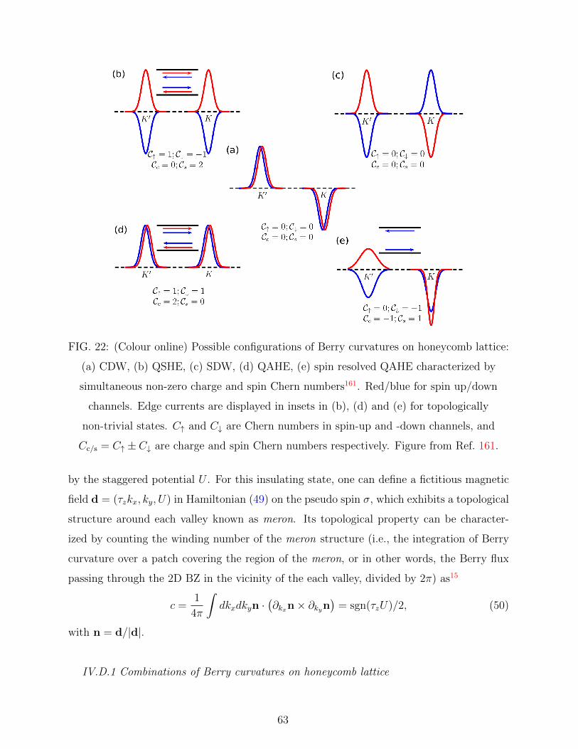
FIG. 22: (Colour online) Possible configurations of Berry curvatures on honeycomb lattice:
(a) CDW, (b) QSHE, (c) SDW, (d) QAHE, (e) spin resolved QAHE characterized by
simultaneous non-zero charge and spin Chern numbers161. Red/blue for spin up/down
channels. Edge currents are displayed in insets in (b), (d) and (e) for topologically
non-trivial states. C↑ and C↓ are Chern numbers in spin-up and -down channels, and
Cc/s = C↑ ± C↓ are charge and spin Chern numbers respectively. Figure from Ref. 161.
by the staggered potential U . For this insulating state, one can define a fictitious magnetic
field d = (τzkx, ky, U) in Hamiltonian (49) on the pseudo spin σ, which exhibits a topological
structure around each valley known as meron. Its topological property can be character-
ized by counting the winding number of the meron structure (i.e., the integration of Berry
curvature over a patch covering the region of the meron, or in other words, the Berry flux
passing through the 2D BZ in the vicinity of the each valley, divided by 2π) as15
c =1
4π
∫dkxdkyn ·
(∂kxn× ∂kyn
)= sgn(τzU)/2, (50)
with n = d/|d|.
IV.D.1 Combinations of Berry curvatures on honeycomb lattice
63

For a staggered electric potential Helec = V σz where V is a constant, the signs of the Berry
curvature around two valleys are opposite, as seen in Eq. (50), which gives a topologically
trivial insulator called a charge density wave (CDW) as displayed in Fig. 22(a). On the
other hand, if a staggered magnetic flux is introduced to spinless electrons on honeycomb
lattice37, the staggered potential term can be written as Hsf = tτzσz (around two valleys),
which depends on the valley variable in contrast to the staggered electric field. Since the
topological charges are now given by c = sgn(t)/2, the Berry curvatures around two valleys
are aligned, which characterizes a QAHE state (see Fig. 22(d) where spin is included in
addition to the Haldane model). This staggered field can be generated by shining circularly
polarized light on graphene, as revealed by the Floquet theorem202. Taking into account
the true spin degree of freedom, the SOC term of Hso = λszτzσz can also be included as
suggested in the Kane-Mele model39, and the SOC term again takes the form of a staggered
field, and depends additionally on spin variable sz. In this case, the Berry curvatures around
two valleys in the spin up and down channels are aligned individually and oppositely for
different spin channels, resulting in the configuration in Fig. 22(b), which characterizes the
QSHE state39. Antiferromagnetic (AFM) exchange field Hafm = Mszσz is another possible
staggered field, which reverses the sign of the Berry curvature in the spin-down channel for
both valleys (compared to the CDW state shown in Fig. 22(a), assuming the same sign for
M and V ), resulting in the configuration in Fig. 22(c) associated with a topologically trivial
state called spin density wave (SDW). Coupling of the valley degree of freedom to the AFM
order in manganese chalcogenophosphates was recently discussed203.
We observe that the configuration of Berry curvature given in Fig. 22(e) corresponds to
an additional topological state161 (see also204), by flipping the sign of the Berry curvature
around K′ valley in the spin up channel from the CDW state. In contrast to QSHE with a
non-zero spin Chern number Cs = C↑ − C↓205,206, which is equivalent to the Z2 index, and
QAHE with a non-zero charge Chern number Cc = C↑ + C↓, this state is characterized by
simultaneous non-zero charge and spin Chern numbers. We may call the state in Fig. 22(e)
spin-resolved QAHE, as opposed to other QAHE states where spin information is lost.
Note that configurations of the Berry curvature in Figs. 22(a), (b), (c) and (d) are con-
verted to each other by flipping the sign of two Berry curvatures either at the same valley
or with the same spin. This reflects certain symmetries in these states: TRS in Fig. 22(a),
TRS and spacial IS in Fig. 22(b), IS in Fig. 22(d), and the combination of TRS and IS in
64
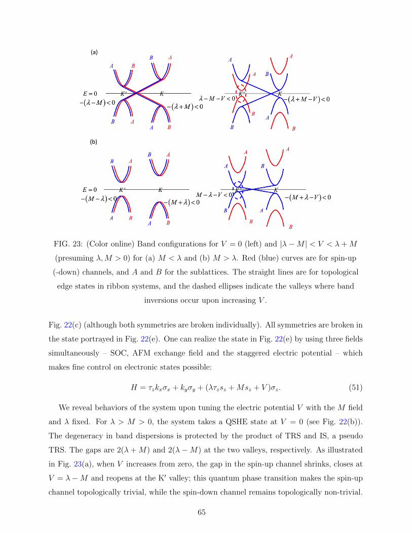
FIG. 23: (Color online) Band configurations for V = 0 (left) and |λ−M | < V < λ+M
(presuming λ,M > 0) for (a) M < λ and (b) M > λ. Red (blue) curves are for spin-up
(-down) channels, and A and B for the sublattices. The straight lines are for topological
edge states in ribbon systems, and the dashed ellipses indicate the valleys where band
inversions occur upon increasing V .
Fig. 22(c) (although both symmetries are broken individually). All symmetries are broken in
the state portrayed in Fig. 22(e). One can realize the state in Fig. 22(e) by using three fields
simultaneously – SOC, AFM exchange field and the staggered electric potential – which
makes fine control on electronic states possible:
H = τzkxσx + kyσy + (λτzsz +Msz + V )σz. (51)
We reveal behaviors of the system upon tuning the electric potential V with the M field
and λ fixed. For λ > M > 0, the system takes a QSHE state at V = 0 (see Fig. 22(b)).
The degeneracy in band dispersions is protected by the product of TRS and IS, a pseudo
TRS. The gaps are 2(λ + M) and 2(λ−M) at the two valleys, respectively. As illustrated
in Fig. 23(a), when V increases from zero, the gap in the spin-up channel shrinks, closes at
V = λ−M and reopens at the K′ valley; this quantum phase transition makes the spin-up
channel topologically trivial, while the spin-down channel remains topologically non-trivial.
65

This QAHE state is possible since the electric field V breaks the IS, therefore breaking the
pseudo TRS. When V increases further, the gap in the spin-down channel shrinks, closes at
V = λ + M and reopens at K valley (not shown explicitly). This second quantum phase
transition makes the spin-down channel trivial as well, and the system transforms into the
topologically trivial CDW state.
For M > λ > 0, the system is in a topologically trivial SDW state at V = 0 (see
Fig. 22(c)). As seen in Fig. 23(b), when V increases, the gap in the spin-down channel
shrinks, closes at V = M−λ and reopens at the K′ valley, which brings the spin-down channel
into a topological state. When V increases further, the gap in the spin-down channel shrinks,
closes at V = λ + M and reopens at K valley, which drives the system to the topologically
trivial CDW state. It is clear that the spin-resolved QAHE state is realized when the sizes
(absolute values) of the three fields satisfy the condition of being able to form a triangle,
which indicates clearly that the interplay among the three fields is crucial. In this case the
sign of the total staggered field U = λτzsz + Msz + V at one valley in one spin channel
is opposite to the other three cases, which yields the configuration of Berry curvature in
Fig. 22(e).
The above discussions for the possible topological phases in honeycomb lattice by fine
tuning of parameters can be generally applied to many different material systems, such
as graphene144–152, silicene153–155, perovskite bilayers156–162, etc. Valleys, as an additional
degree of freedom of electrons on honeycomb lattice, have attracted considerable interest,
for which valleytronics has been coined as a new concept207,208. We will leave the discussions
of topological states in graphene and silicene to readers, and in the following, we concentrate
on the perovskite bilayer systems, which are interesting and promising due to the presence
of transition metal elements.
IV.D.2 Honeycomb lattices by perovskite structures
Material realization of topological insulators (TI) has been mainly focused on narrow
band-gap semiconductors with heavy elements such as Hg or Bi, in which the electronic
properties are dominated by s and p orbitals. Recently a completely different materials class
– heterostructures of transition-metal oxides (TMOs) involving d electrons – was proposed156.
The TMO heterostructures are readily available due to achievements in the fields of oxide
66

FIG. 24: (Color online) Perovskite structure as a buckled honeycomb lattice grown along
the [111] crystal direction. Adapted from Ref. 156.
superlattices and oxide electronics209–211. The sample of layered structure of TMOs can be
obtained with atomic precision212–214. This make the fine tuning of sample properties, such
as the lattice constant, carrier density, SOC and electron-electron correlation, very plausible.
Possible 2D TIs have been proposed for bilayers of perovskite-type TMOs grown along the
[111] direction of the crystallographic axis156.
Perovskite compounds215 are in the chemical formula of ABO3, where A stands for alkaline
or rare earth metal, B stands for transition metal (TM) and O stands for oxygen. Its
structure is shown in Fig. 24(a) and (b). The ideal oxygen octahedral crystal field splits
the TM d orbitals into eg (with d3z2−r2 and dx2−y2 orbitals) and t2g (with dyz, dzx and
dxy) manifolds, separated by ∼3eV in energy. Such crystal geometry usually is not good
for band inversion. However, for a bilayer of the perovskite structure grown along [111]
direction156, the TM ions are on a buckled honeycomb lattice as shown in Fig. 24(c). Based
on tight-banding models and first-principles calculations, D. Xiao et al. have demonstrated
that both t2g and eg orbitals can generate topologically non-trivial states for TM ions on
such structure. Especially, they showed that LaAuO3 bilayers sandwiched by two LaAlO3
substrates might possess a topologically non-trivial gap around 0.15 eV156.
Various possible topological phases have been explored for the perovskite bilayer sys-
tems158–160. Except the QSH phase, the QAH phase can be readily expected by breaking
the TRS, as discussed before. Thanks to the presence of transition metal elements, different
magnetic orderings may be realized in such systems with no need of additional doping. If
the strong electron interaction among the d electrons is properly taken into account, we can
67

expect more interesting physics157 for such honeycomb lattices formed by bilayer perovskite
structures. In a recent study, it was predicted162 by the LDA+Gutzwiller method216, that
(111) LaCoO3 bilayer grown on SrTiO3 substrate may support the QAHE. Here, the inter-
play between SOC and Coulomb interaction stabilizes a robust FM insulating state, which
is a Chern insulator with non-zero Chern number. It was pointed out in this study, that
the SOC splitting (which is usually not strong for 3d elements) can be greatly enhanced
by the strong Coulomb interaction. It has also been revealed that the possibility of some
intriguing phenomena, such as fractional quantum Hall effect, associated with the nearly
flat topologically non-trivial bands can be found in eg systems156.
The perovskite bilayer structure can also be used to generate the spin-resolved QAHE
state. Choosing elements adequately, one can fill t2g orbitals while leaving eg orbitals par-
tially occupied, and the 10Dq gap (crystal-field splitting) will prevent t2g orbitals from
participating in the low-energy physics. For an atomic sheet of buckled honeycomb lattice,
the two B atoms in a unit cell contribute four eg orbits in total. The band structure for these
four orbitals is shown in Fig. 25(a) based on the tight-binding Hamiltonian with the hopping
integrals given by the Slater-Koster formula161. Two dispersive bands are contributed from
d8,9(t62ge2,3g ), which cross each other linearly and form the desired Dirac cones at K and K′
due to the honeycomb structure.
A candidate perovskite material which generates d8 electrons is LaAuO3, wherein Au
takes the +3 charge state. In order to generate an AFM exchange field, one can sandwich
the atomic sheet of buckled honeycomb lattice with d8 electrons by two thick layers of
insulating perovskite material grown in the [111] direction. A candidate material for the
substrates is LaCrO3, a Mott insulator with G-type AFM order, which induces opposite
exchange fields on the two sublattices in the buckled honeycomb lattice. The large Mott
gap of LaCrO3 prevents undesired influences on the Dirac behavior of d8,9 electrons except
for the exchange field. Since La is chosen as the common A-site cation, the lattice mismatch
between substrate and the targeting atomic sheet is minimal. First-principles calculations
were performed in terms of VASP217 code with a supercell of (La2Au2O6)/(La2Cr2O6)5 shown
in Fig. 25(b). As displayed in Fig. 25(c), the black bands are mainly from the substrate
LaCrO3 with a large gap of 3eV, characteristic of a Mott insulator. The bands inside the
Mott gap are contributed by the eg electrons of Au+3 ions. There are two almost flat bands
and two dispersive bands, as captured by the tight-binding Hamiltonian (see Fig. 25(a)).
68

FIG. 25: (Color online) (a) Noninteracting tight-binding band structure of the eg system,
where each band is labeled with the corresponding electron configuration if it is occupied.
Inset shows the two eg orbits. (b) Schematic of a unit cell (La2Au2O6)/(La2Cr2O6)5. (c)
Band structures based on first-principles calculation. Figures from Ref. 161.
Gaps are opened at K and K′ since the Dirac electrons now feel the AFM exchange field from
LaCrO3 and SOC. The two gaps are different in magnitude and given explicitly by 2(M+λ)
and 2(M-λ) respectively (see Fig. 23(b) for V = 0), from which one obtains M = 0.166eV
and λ = 32.91meV for this system. SOC effect is quite large in the present case, due to the
orbital hybridization between the two eg orbits in the new frame along the [111] crystalline
direction. All the states in Fig. 25(b) are doubly degenerate due to the product symmetry
of TRS and IS. If a gate electric field is applied along the [111] direction, the Au ions in the
buckled honeycomb lattice should experience staggered electric potentials. By increasing the
69

electric potential, the system should be driven into the spin-resolved QAHE, as summarized
in Fig. 23(b). The required electric field is on the order of 0.1V/A. As the maximal non-
trivial gap is given by 2λ ' 600K, this topological state in the LaCrO3/LaAuO3 superlattice
may remain stable even around room temperature. Interaction driven QAHE phase can also
be found in SrTiO3/LaCoO3/SrTiO3 quantum well as discussed in detail in Ref. 218.
It is worth noticing that, although the edge current of the spin-resolved QAHE state is
fully spin polarized, the total system does not show any net spin magnetization, since the
numbers of occupied states in the two spin channels of the buckled honeycomb lattice are the
same, and the substrates are AFM insulators. The spin polarization of the edge current can
be reversed by the gating electric field, which is superior for future spintronic applications.
V. DISCUSSIONS AND FUTURE PROSPECTS
At this stage, the quantum Hall trio (namely, quantum Hall effect, quantum spin Hall ef-
fect, and quantum anomalous Hall effect) has been completed.219 Looking back to history, it
was a long term exploration towards the final realization of QAHE. First, the understanding
of the Berry phase mechanism of intrinsic AHE was an important step, because it established
the link between the AHE and the topological properties of electronic structure. Second,
the rapid progresses in the field of topological insulators strongly stimulated the studies on
QAHE. Third, first-principles calculations play important roles in predicting and selecting
candidate materials and systems. This also establishes a nice example that theoretical and
computational studies can in some cases really go ahead of and greatly help experiments.
Finally, the well-controlled growth and magnetic doping of high quality samples and trans-
port measurement at ultra-low temperature make the experiments possible, thanks to the
progress of modern experimental technology. All these aspects combined together finally
gave birth to the QAHE.
On the other hand, the successful realization of QAHE is not the end of the story. Instead,
we believe this success will inspire more extensive research in this field. Two issues become
immediately important for future studies:
(1) How can we realize a higher plateau with a Chern number larger than 1?
(2) How can we increase the temperature range of QAHE (it is now observed only in the
tens mK range)?
70

From the theoretical point of view, the QAH states with higher Chern numbers can be
derived in a way similar to that described in section VI.B if the magnetic exchange field can
be made larger185,220. Larger exchange field will, in general, generate more band inversions
among sub-bands and thus induce higher Chern numbers. While in practice this idea is very
difficult, because the system with large enough exchange field will usually become completely
metallic before the second plateau state appears. An alternative way to realize the QAHE
with a high Chern number is to start with materials that have multiple band inversion
regimes in the BZ. An interesting proposal is the magnetically doped topological crystalline
insulators (Pb,Sn)(Te,Se), which have band inversions around all the four T points in the
BZ221. Similar to the situation in Bi2Se3 family compounds, here the band inversions appear
between p-bands with opposite parity, and the Van Vleck mechanism also works, which can
lead to a stable FM semiconductor ground state after magnetic doping. Therefore, for thin
films of this system with proper thickness, it is possible to realize the QAHE with a Chern
number between ±4221.
The experimental observation of QAHE in thin films of Cr-doped (Bi,Sb)2Te3 requires an
extremely low temperature (approximately 30 mK), which hinders realistic applications141.
This is presumably due to the small band gap opened by exchange coupling and the low
carrier mobility of 760 cm2/Vs in the sample. Therefore, searching for realistic systems with
non-trivial band structures, strong exchange coupling and high sample quality is essential
to realize the QAH effect at a higher temperature. Liu et al. proposed to realize QAHE
in a more conventional diluted magnetic semiconductor, the Mn-doped InAs/GaSb type II
quantum well, which has a higher carrier mobility of 6000 cm2/Vs and a predicted FM
transition temperature of 30 K140. Other theoretical proposes for high temperature QAHE
systems are based on the stanene and germanene materials. These two materials are re-
cently predicted to be QSHI with a large insulating gap222. The QSH phase appears due
to an energy inversion between the Sn(Ge)-s and Sn(Ge)-pxy bands, which have opposite
parities and lead to a sizable bulk gap of 0.3 eV. In Ref. 223, S. C. Wu, et al, proposed
that half-passivated stanene and germanene become Chern insulators with energy gaps of
0.34 and 0.06 eV, respectively. The proposed FM order in this system comes from the
unpassivated sublattice that exhibits dangling bonds. Strong coupling between the spin-
polarized dangling bond states and the inherent inverted bands opens a considerable energy
gap. The estimated mean-field Curie temperature is as high as 243 K and 509 K for Sn
71

and Ge lattices, respectively. In spite of those theoretical proposals, it is still challenging to
reach QAHE at higher temperature experimentally. To achieve this goal, searching for new
host materials with simpler electronic structure, easier synthesis and less extreme growth
conditions is necessary.
The QAHE and Chern insulators can be also helpful for the possible realization of
Majorana fermions (MF)224, which are exotic charge-neutral particles that are their own
antiparticles. In recent years, Majorana fermions have been intensively studied in the
field of condensed matter physics due to their importance to both fundamental science
and potential applications in topological quantum computing. Theoretically, Majorana
fermions have been predicted to exist in several spin orbit coupled superconducting systems,
such as superconductor-topological insulator interfaces73, semiconductor-superconductor
heterostructures225–227, nanotube-superconductor devices228, half-metal-superconductor in-
terface79, etc. Experimentally, great efforts have been made in this direction, and some
important evidence has been successfully observed229,230. On the other hand, in Ref. 75, a
different way to generate Majorana fermions is proposed in a hybrid device that consists of
a QH or QAH insulator layer in proximity to a fully gapped superconductor layer on top. In
this case, it can generally be expected that a chiral topological superconductor phase with
an odd number of chiral Majorana edge modes will exist. Compared to the QH system in
the proposal, the QAH system has the advantage that it does not require external magnetic
field, which makes the realization of superconductor proximity effect much easier. The Ma-
jorana zero mode in a model combined with a QAHE system and an s-wave superconductor
is also discussed in Ref. 231.
In summary of the present paper, we have reviewed the history of achieving the QAHE.
In 1880, E. H. Hall found the anomalous Hall effect, 17 years before the discovery of the
electron. In the following 100 years, however, the developments in this field, particularly for
the understanding of AHE, were slow. There were debates on whether intrinsic or extrinsic
contribution is dominant. The breakthrough was the discovery of the QHE in 1980, from
which people learned that there exist new quantum states characterized by the topology of
electronic structures. The concept of the Berry phase, established in 1984 by M. V. Berry, is
the solid base of various topological quantum states. We have reviewed how the Berry phase
is related to the AHE, QHE, QAHE, QSHE, 3D TIs and 3D Weyl/Dirac semimetals. Such
a unified view has led us to a unified scheme, called the Wilson loop method, in calculating
72

various topological invariants, including the Chern number, Z2 index, mirror Chern number
and Fermi surface Chern number. This method is efficient in rigorously determining the
topology of real materials. However, in practical calculations, the band inversion mecha-
nism is much more intuitive and efficient in predicting, selecting and designing candidate
topological materials. Finally, we have listed the necessary and complete four conditions
for realizing the QAHE. Following these conditions, we have demonstrated several ways to
achieve the QAHE. The theoretical prediction for the QAHE in magnetic-ion Cr and Fe
doped Bi2Se3 and Bi2Te3 family TIs has been recently confirmed by experimental observa-
tion. The key difference of this scheme from other proposals is the FM ordering of Cr and
Fe dopants induced by the van Vleck paramagnetism, which makes this proposal successful.
VI. ACKNOWLEDGEMENTS
H.M.W., X.D. and Z.F. are supported by the National Science Foundation of China, the
973 program of China (No. 2011CBA00108 and 2013CB921700), and the “Strategic Priority
Research Program (B)” of the Chinese Academy of Sciences (No. XDB07020100). R.Y. and
X.H. are supported by the WPI Initiative on Materials Nanoarchitectonics, and partially
by Grant-in-Aid for Scientific Research under the Innovative Area “Topological Quantum
Phenomena” (No.25103723), MEXT, Japan.
VII. REFERENCES
1 E.H. Hall, “On the new action of magnetism on a permanent electric current,” Philosophical
Magazine Series 5 10, 301–328 (1880).
2 E.H. Hall, “On the Rotational coefficient in nickel and cobalt,” Philosophical Magazine Series
5 12, 157–172 (1881).
3 A. Kundt, “On the Hall effect in ferromagnetic materials,” Wied. Ann. 49, 257 (1893).
73

4 Emerson M. Pugh, “Hall effect and the magnetic properties of some ferromagnetic materials,”
Phys. Rev. 36, 1503–1511 (1930).
5 E. M. Pugh and T. W. Lippert, “Hall e.m.f. and intensity of magnetization,” Phys. Rev. 42,
709–713 (1932).
6 G. Bergmann, “Transition from Pauli paramagnetism to band ferromagnetism in very thin Ni
films,” Phys. Rev. Lett. 41, 264–267 (1978).
7 H. Ohno, H. Munekata, T. Penney, S. von Molnr, and L. L. Chang, “Magnetotransport
properties of p-type (In,Mn)As diluted magnetic III-V semiconductors,” Phys. Rev. Lett. 68,
2664–2667 (1992).
8 H. Ohno, A. Shen, F. Matsukura, A. Oiwa, A. Endo, S. Katsumoto, and Y. Iye, “(Ga,Mn)As:
a new diluted magnetic semiconductor based on GaAs,” Applied Physics Letters 69, 363–365
(1996).
9 T. Jungwirth, Q. Niu, and A. H. MacDonald, “Anomalous Hall effect in ferromagnetic semi-
conductors,” Phys. Rev. Lett. 88, 207208 (2002).
10 M. Onoda and N. Nagaosa, “Topological nature of anomalous Hall effect in ferromagnets,” J.
Phys. Soc. J. 71, 19–22 (2002).
11 Z. Fang, N. Nagaosa, K. S. Takahashi, A. Asamitsu, R. Mathieu, T. Ogasawara, H. Ya-
mada, M. Kawasaki, Y. Tokura, and K. Terakura, “The anomalous Hall effect and magnetic
monopoles in momentum space,” Science 302, 92–95 (2003).
12 Y. G. Yao, L. Kleinman, A. H. MacDonald, J. Sinova, T. Jungwirth, D. S. Wang, E. G. Wang,
and Q. Niu, “First principles calculation of anomalous Hall conductivity in ferromagnetic bcc
Fe,” Phys. Rev. Lett. 92, 037204 (2004).
13 J. Sinova, T. Jungwirth, and J. Cerne, “Magneto-transport and magneto-optical properties of
ferromagnetic (III,Mn)V semiconductors: a review,” International Journal of Modern Physics
B 18, 1083–1118 (2004).
14 N. Nagaosa, J. Sinova, S. Onoda, A. H. MacDonald, and N. P. Ong, “Anomalous Hall effect,”
Rev. Mod. Phys. 82, 1539–1592 (2010).
15 D. Xiao, M. C. Chang, and Q. Niu, “Berry phase effects on electronic properties,” Rev. Mod.
Phys. 82, 1959 (2010).
16 M. V. Berry, “Quantal phase factors accompanying adiabatic changes,” Pro. R. Soc. Lond. A
392, 45–57 (1984).
74

17 R. Karplus and J. M. Luttinger, “Hall effect in ferromagnetics,” Phys. Rev. 95, 1154–1160
(1954).
18 J. Smit, “The spontaneous Hall effect in ferromagnetics I,” Physica 21, 877–887 (1955).
19 J. Smit, “The spontaneous Hall effect in ferromagnetics II,” Physica 24, 39–51 (1958).
20 L. Berger, “Side-jump mechanism for the Hall effect of ferromagnets,” Phys. Rev. B 2, 4559–
4566 (1970).
21 S. Onoda, N. Sugimoto, and N. Nagaosa, “Intrinsic versus extrinsic anomalous Hall effect in
ferromagnets,” Phys. Rev. Lett. 97, 126602 (2006).
22 T. Miyasato, N. Abe, T. Fujii, A. Asamitsu, S. Onoda, Y. Onose, N. Nagaosa, and Y. Tokura,
“Crossover behavior of the anomalous Hall effect and anomalous nernst effect in itinerant
ferromagnets,” Phys. Rev. Lett. 99, 086602 (2007).
23 Y. Tian, L. Ye, and X. F. Jin, “Proper scaling of the anomalous Hall effect,” Phys. Rev. Lett.
103, 087206 (2009).
24 L. Ye, Y. Tian, X. F. Jin, and D. Xiao, “Temperature dependence of the intrinsic anomalous
Hall effect in nickel,” Phys. Rev. B 85, 220403 (2012).
25 C. G. Zeng, Y. G. Yao, Q. Niu, and H. H. Weitering, “Linear magnetization dependence of
the intrinsic anomalous Hall effect,” Phys. Rev. Lett. 96, 037204 (2006).
26 K. v. Klitzing, G. Dorda, and M. Pepper, “New method for high-accuracy determination of
the fine-structure constant based on quantized Hall resistance,” Phys. Rev. Lett. 45, 494–497
(1980).
27 F. Wilczek and A. Shapere, Geometric phases in physics, Vol. 5 (World Scientific, 1989).
28 D. J. Thouless, M. Kohmoto, M. P. Nightingale, and M. den Nijs, “Quantized Hall conductance
in a two-dimensional periodic potential,” Phys. Rev. Lett. 49, 405–408 (1982).
29 R. E. Prange and S. M. Girvin, The Quantum Hall effect (Springer-Verlag, 1987).
30 M. Stone, Quantum Hall Effect (World Scientific, 1992).
31 Y. G. Yao, Y. C. Liang, D. Xiao, Q. Niu, S. Q. Shen, X. Dai, and Z. Fang, “Theoretical
evidence of the Berry-phase mechanism in anomalous Hall transport: First-principles studies
of CuCr2Se4−xBrx ,” Phys. Rev. B 75, 020401 (2007).
32 W. L. Lee, S. Watauchi, V. L. Miller, R. J. Cava, and N. P. Ong, “Dissipationless Anomalous
Hall Current in the Ferromagnetic Spinel CuCr2Se4−xBrx,” Science 303, 1647–1649 (2004).
75

33 R. D. King-Smith and D. Vanderbilt, “Theory of polarization of crystalline solids,” Phys. Rev.
B 47, 1651–1654 (1993).
34 R. Resta, “Macroscopic polarization in crystalline dielectrics: the geometric phase approach,”
Rev. Mod. Phys. 66, 899–915 (1994).
35 X. J. Wang, J. R. Yates, I. Souza, and D. Vanderbilt, “Ab initio calculation of the anomalous
Hall conductivity by Wannier interpolation,” Phys. Rev. B 74, 195118 (2006).
36 X. J. Wang, D. Vanderbilt, J. R. Yates, and I. Souza, “Fermi-surface calculation of the
anomalous Hall conductivity,” Phys. Rev. B 76, 195109 (2007).
37 F. D. M. Haldane, “Model for a quantum Hall effect without landau levels: Condensed-matter
realization of the “Parity anomaly”,” Phys. Rev. Lett. 61, 2015–2018 (1988).
38 C. L. Kane and E. J. Mele, “Z2 topological order and the quantum spin Hall effect,” Phys.
Rev. Lett. 95, 146802 (2005).
39 C. L. Kane and E. J. Mele, “Quantum spin Hall effect in graphene,” Phys. Rev. Lett. 95,
226801 (2005).
40 B. A. Bernevig and S. C. Zhang, “Quantum spin Hall effect,” Phys. Rev. Lett. 96, 106802
(2006).
41 B. A. Bernevig, T. L. Hughes, and S. C. Zhang, “Quantum spin Hall effect and topological
phase transition in HgTe quantum wells,” Science 314, 1757–1761 (2006).
42 M. Konig, S. Wiedmann, C. Brune, A. Roth, H. Buhmann, L. W. Molenkamp, X. L. Qi,
and S. C. Zhang, “Quantum spin Hall insulator state in HgTe quantum wells,” Science 318,
766–770 (2007).
43 H. J. Zhang, C. X. Liu, X. L. Qi, X. Dai, Z. Fang, and S. C. Zhang, “Topological insulators in
Bi2Se3, Bi2Te3 and Sb2Te3 with a single dirac cone on the surface,” Nature Physics 5, 438–442
(2009).
44 P. Roushan, J. Seo, C. V. Parker, Y. S. Hor, D. Hsieh, D. Qian, A. Richardella, M. Z. Hasan,
R. J. Cava, and A. Yazdani, “Topological surface states protected from backscattering by
chiral spin texture,” Nature 460, 1106–1109 (2009).
45 T. Zhang, P. Cheng, X. Chen, J. F. Jia, X. C. Ma, K. He, L. L. Wang, H. J. Zhang, X. Dai,
Z. Fang, X. C. Xie, and Q. K. Xue, “Experimental demonstration of topological surface states
protected by time-reversal symmetry,” Phys. Rev. Lett. 103, 266803 (2009).
76

46 Y. Xia, D. Qian, D. Hsieh, L. Wray, A. Pal, H. Lin, A. Bansil, D. Grauer, Y. S. Hor, R. J.
Cava, and M. Z. Hasan, “Observation of a large-gap topological-insulator class with a single
Dirac cone on the surface,” Nature Physics 5, 398–402 (2009).
47 Y. L. Chen, J. G. Analytis, J.-H. Chu, Z. K. Liu, S.-K. Mo, X. L. Qi, H. J. Zhang, D. H.
Lu, X. Dai, Z. Fang, S. C. Zhang, I. R. Fisher, Z. Hussain, and Z.-X. Shen, “Experimental
realization of a three-dimensional topological insulator, Bi2Te3,” Science 325, 178–181 (2009).
48 Z. Alpichshev, J. G. Analytis, J.-H. Chu, I. R. Fisher, Y. L. Chen, Z. X. Shen, A. Fang,
and A. Kapitulnik, “STM imaging of electronic waves on the surface of Bi2Te3: Topologically
protected surface states and hexagonal warping effects,” Phys. Rev. Lett. 104, 016401 (2010).
49 M. Z. Hasan and C. L. Kane, “Colloquium: Topological insulators,” Rev. Mod. Phys. 82,
3045–3067 (2010).
50 X. L. Qi and S. C. Zhang, “Topological insulators and superconductors,” Rev. Mod. Phys. 83,
1057–1110 (2011).
51 I. Knez, R. R. Du, and G. Sullivan, “Evidence for helical edge modes in inverted InAs/GaSb
quantum wells,” Phys. Rev. Lett. 107, 136603 (2011).
52 H. Beidenkopf, P. Roushan, J. Seo, L. Gorman, I. Drozdov, Y. S. Hor, R. J. Cava, and A. Yaz-
dani, “Spatial fluctuations of helical Dirac fermions on the surface of topological insulators,”
Nature Physics 7, 939–943 (2011).
53 Y. Ando, “Topological Insulator Materials,” J. Phys. Soc. Jpn. 82, 102001 (2013).
54 A. P. Schnyder, S. Ryu, A. Furusaki, and A. W. W. Ludwig, “Classification of topological
insulators and superconductors in three spatial dimensions,” Phys. Rev. B 78, 195125 (2008).
55 X. G. Wan, A. M. Turner, A. Vishwanath, and S. Y. Savrasov, “Topological semimetal and
fermi-arc surface states in the electronic structure of pyrochlore iridates,” Phys. Rev. B 83,
205101 (2011).
56 G. Xu, H. M. Weng, Z. J. Wang, X. Dai, and Z. Fang, “Chern Semimetal and the Quantized
Anomalous Hall Effect in HgCr2Se4,” Phys. Rev. Lett. 107, 186806 (2011).
57 A. A. Burkov and L. Balents, “Weyl Semimetal in a Topological Insulator Multilayer,” Phys.
Rev. Lett. 107, 127205 (2011).
58 A. A. Zyuzin, S. Wu, and A. A. Burkov, “Weyl semimetal with broken time reversal and
inversion symmetries,” Phys. Rev. B 85, 165110 (2012).
77

59 Z. J. Wang, Y. Sun, X. Q. Chen, C. Franchini, G. Xu, H. M. Weng, X. Dai, and Z. Fang,
“Dirac semimetal and topological phase transitions in A3Bi (A=Na, K, Rb),” Phys. Rev. B
85, 195320 (2012).
60 S. M. Young, S. Zaheer, J. C. Y. Teo, C. L. Kane, E. J. Mele, and A. M. Rappe, “Dirac
semimetal in three dimensions,” Phys. Rev. Lett. 108, 140405 (2012).
61 A. M. Turner, Y. Zhang, R. S. K. Mong, and A. Vishwanath, “Quantized response and
topology of magnetic insulators with inversion symmetry,” Phys. Rev. B 85, 165120 (2012).
62 Z. J. Wang, H. M. Weng, Q. S. Wu, X. Dai, and Z. Fang, “Three-dimensional Dirac semimetal
and quantum transport in Cd3As2,” Phys. Rev. B 88, 125427 (2013).
63 Z. K. Liu, B. Zhou, Y. Zhang, Z. J. Wang, H. M. Weng, D. Prabhakaran, S. K. Mo, Z. X. Shen,
Z. Fang, X. Dai, Z. Hussain, and Y. L. Chen, “Discovery of a Three-Dimensional Topological
Dirac Semimetal, Na3Bi,” Science 343, 864–867 (2014).
64 Z. K. Liu, J. Jiang, B. Zhou, Z. J. Wang, Y. Zhang, H. M. Weng, D. Prabhakaran, S. K. Mo,
H. Peng, P. Dudin, T. Kim, M. Hoesch, Z. Fang, X. Dai, Z. X. Shen, D. L. Feng, Z. Hussain,
and Y. L. Chen, “A stable three-dimensional topological Dirac semimetal Cd3As2,” Nature
Materials 13, 677–681 (2014).
65 H. M. Yi, Z. J. Wang, C. Y. Chen, Y. G. Shi, Y. Feng, A. J. Liang, Z. J. Xie, S. L. He, J. F. He,
. Y. Peng, X. Liu, Y. Liu, L. Zhao, G. D. Liu, X. L. Dong, J. Zhang, M. Nakatake, M. Arita,
K. Shimada, H. Namatame, M. Taniguchi, Z. Y. Xu, C. T. Chen, X. Dai, Z. Fang, and X. J.
Zhou, “Evidence of Topological Surface State in Three-Dimensional Dirac Semimetal Cd3As2,”
Scientific Reports 4, 6106 (2014).
66 M. Neupane, S. Y. Xu, R. Sankar, N. Alidoust, G. Bian, C. Liu, I. Belopolski, T. R. Chang,
H. T. Jeng, H. Lin, A. Bansil, F. C. Chou, and M. Z. Hasan, “Observation of a three-
dimensional topological Dirac semimetal phase in high-mobility Cd3As2,” Nature Communi-
cations 5, 3786 (2014).
67 B. J. Yang and N. Nagaosa, “Classification of stable three-dimensional dirac semimetals with
nontrivial topology,” Nature Communications 5, 4898 (2014).
68 S. J. Jeon, B. B. Zhou, A. Gyenis, B. E. Feldman, I. Kimchi, A. C. Potter, Q. D. Gibson, R. J.
Cava, A. Vishwanath, and A. Yazdani, “Landau quantization and quasiparticle interference
in the three-dimensional dirac semimetal Cd3As2,” Nature Materials 13, 851–856 (2014).
78

69 S.-Y. Xu, C. Liu, S. K. Kushwaha, R. Sankar, J. W. Krizan, I. Belopolski, M. Neupan, e,
G. Bian, N. Alidoust, T.-R. Chang, H.-T. Jeng, C.-Y. Huang, W.-F. Tsai, H. Lin, P. P.
Shibayev, F. Chou, R. J. Cava, and M. Z. Hasan, “Observation of Fermi arc surface states in
a topological metal,” Science 347, 294–298 (2015).
70 A. A. Burkov, M. D. Hook, and L. Balents, “Topological nodal semimetals,” Phys. Rev. B 84,
235126 (2011).
71 L. Lu, L. Fu, J. D. Joannopoulos, and M. Soljacic, “Weyl points and line nodes in gyroid
photonic crystals,” Nature Photonics 7, 294–299 (2013).
72 Hongming Weng, Yunye Liang, Qiunan Xu, Rui Yu, Zhong Fang, Xi Dai, and Yoshiyuki
Kawazoe, “Topological node-line semimetal in three-dimensional graphene networks,” Phys.
Rev. B 92, 045108 (2015).
73 L. Fu and C. L. Kane, “Superconducting proximity effect and Majorana fermions at the surface
of a topological insulator,” Phys. Rev. Lett. 100, 096407 (2008).
74 X. L. Qi, T. L. Hughes, and S. C. Zhang, “Topological field theory of time-reversal invariant
insulators,” Phys. Rev. B 78, 195424 (2008).
75 X. L. Qi, T. L. Hughes, and S. C. Zhang, “Chiral topological superconductor from the quantum
Hall state,” Phys. Rev. B 82, 184516 (2010).
76 L. Fu and E. Berg, “Odd-Parity Topological Superconductors: Theory and Application to
CuxBi2Se3,” Phys. Rev. Lett. 105, 097001 (2010).
77 Y. S. Hor, A. J. Williams, J. G. Checkelsky, P. Roushan, J. Seo, Q. Xu, H. W. Zandbergen,
A. Yazdani, N. P. Ong, and R. J. Cava, “Superconductivity in CuxBi2Se3 and its Implications
for Pairing in the Undoped Topological Insulator,” Phys. Rev. Lett. 104, 057001 (2010).
78 J. L. Zhang, S. J. Zhang, H. M. Weng, W. Zhang, L. X. Yang, Q. Q. Liu, S. M. Feng, X. C.
Wang, R. C. Yu, and L. Z. Cao, “Pressure-induced superconductivity in topological parent
compound Bi2Te3,” PNAS 108, 24–28 (2011).
79 H. M. Weng, G. Xu, H. J. Zhang, S. C. Zhang, X. Dai, and Z. Fang, “Half-metallic surface
states and topological superconductivity in NaCoO2 from first principles,” Phys. Rev. B 84,
060408 (2011).
80 M. Onoda and N. Nagaosa, “Quantized anomalous Hall effect in two-dimensional ferromagnets:
Quantum Hall effect in metals,” Phys. Rev. Lett. 90, 206601 (2003).
79

81 S. S. Chern, “On the curvatura integra in a riemannian manifold,” The Annals of Mathematics
46, 674 (1945).
82 D. J. Thouless, “Wannier functions for magnetic sub-bands,” Journal of Physics C: Solid State
Physics 17, L325 (1984).
83 T. Thonhauser and D. Vanderbilt, “Insulator/Chern-insulator transition in the Haldane
model,” Phys. Rev. B 74, 235111 (2006).
84 C. Brouder, G. Panati, M. Calandra, C. Mourougane, and N. Marzari, “Exponential localiza-
tion of wannier functions in insulators,” Phys. Rev. Lett. 98, 046402 (2007).
85 A. A. Soluyanov and D. Vanderbilt, “Wannier representation of Z2 topological insulators,”
Phys. Rev. B 83, 035108 (2011).
86 Y. Hatsugai, “Edge states in the integer quantum Hall effect and the Riemann surface of the
Bloch function,” Phys. Rev. B 48, 11851–11862 (1993).
87 A. M. Essin and V. Gurarie, “Bulk-boundary correspondence of topological insulators from
their respective Green’s functions,” Phys. Rev. B 84, 125132 (2011).
88 A. H. MacDonald and P. Streda, “Quantized Hall effect and edge currents,” Phys. Rev. B 29,
1616–1619 (1984).
89 B. I. Halperin, “Quantized Hall conductance, current-carrying edge states, and the existence
of extended states in a two-dimensional disordered potential,” Phys. Rev. B 25, 2185–2190
(1982).
90 Z. C. Gu and X. G. Wen, “Tensor-entanglement-filtering renormalization approach and
symmetry-protected topological order,” Phys. Rev. B 80, 155131 (2009).
91 L. Fu and C. L. Kane, “Time reversal polarization and a Z2 adiabatic spin pump,” Phys. Rev.
B 74, 195312 (2006).
92 R. Yu, X. L. Qi, A. Bernevig, Z. Fang, and X. Dai, “Equivalent expression of Z2 topological
invariant for band insulators using the non-Abelian Berry connection,” Phys. Rev. B 84, 75119
(2011).
93 L. Fu, C. L. Kane, and E. J. Mele, “Topological insulators in three dimensions,” Phys. Rev.
Lett. 98, 106803 (2007).
94 J. Moore and L. Balents, “Topological invariants of time-reversal-invariant band structures,”
Phys. Rev. B 75, 121306 (2007).
80

95 R. Roy, “Topological phases and the quantum spin Hall effect in three dimensions,” Phys. Rev.
B 79, 195322 (2009).
96 G. E. Volovik, The Universe in a Helium Droplet (Oxford, 2009).
97 J. Zak, “Berry’s phase for energy bands in solids,” Phys. Rev. Lett. 62, 2747–2750 (1989).
98 H. Weyl, “Elektron und gravitation. i,” Zeitschrift fur Physik 56, 330–352 (1929).
99 H. B. Nielsen and M. Ninomiya, “Absence of neutrinos on a lattice: (I). Proof by homotopy
theory,” Nuclear Physics B 185, 20–40 (1981).
100 H. B. Nielsen and M. Ninomiya, “Absence of neutrinos on a lattice: (II). Intuitive topological
proof,” Nuclear Physics B 193, 173–194 (1981).
101 F. D. M. Haldane, “Attachment of surface ”Fermi arcs” to the bulk Fermi surface: ”Fermi-level
plumbing” in topological metals,” arXiv:1401.0529 [cond-mat] (2014).
102 L. Balents, “Weyl electrons kiss,” Physics 4, 36 (2011).
103 S. Murakami, “Phase transition between the quantum spin Hall and insulator phases in 3d:
emergence of a topological gapless phase,” New J. Phys. 9, 356 (2007).
104 W. Zhang, R. Yu, H. J. Zhang, X. Dai, and Z. Fang, “First-principles studies of the three-
dimensional strong topological insulators Bi2Te3, Bi2Se3 and Sb2Te3,” New J. Phys. 12, 065013
(2010).
105 J. P. Liu and D. Vanderbilt, “Weyl semimetals from noncentrosymmetric topological insula-
tors,” Phys. Rev. B 90, 155316 (2014).
106 Gabor B. Halasz and L. Balents, “Time-reversal invariant realization of the Weyl semimetal
phase,” Phys. Rev. B 85, 035103 (2012).
107 M. Hirayama, R. Okugawa, S. Ishibashi, S. Murakami, and T. Miyake, “Weyl node and spin
texture in trigonal tellurium and selenium,” ArXiv:1409.7517 (2014), arXiv:1409.7517 [cond-
mat.mtrl-sci].
108 Hongming Weng, Chen Fang, Zhong Fang, B. A. Bernevig, and X. Dai, “Weyl semimetal phase
in noncentrosymmetric transition-metal monophosphides,” Phys. Rev. X 5, 011029 (2015).
109 S.-M. Huang, S.-Y. Xu, I. Belopolski, C.-C. Lee, G. Chang, B. Wang, N. Alidoust, G. Bian,
M. Neupane, A. Bansil, H. Lin, and M. Zahid Hasan, “An inversion breaking Weyl semimetal
state in the TaAs material class,” Nature Communications 6, 7383 (2015).
110 X. L. Qi, Y. S. Wu, and S. C. Zhang, “Topological quantization of the spin Hall effect in
two-dimensional paramagnetic semiconductors,” Phys. Rev. B 74, 085308 (2006).
81

111 Y. Chen, D. L. Bergman, and A. A. Burkov, “Weyl fermions and the anomalous Hall effect
in metallic ferromagnets,” Phys. Rev. B 88, 125110 (2013).
112 A. A. Burkov, “Topological response in ferromagnets,” Phys. Rev. B 89, 155104 (2014).
113 A. A. Burkov, “Anomalous Hall effect in weyl metals,” Phys. Rev. Lett. 113, 187202 (2014).
114 B. A. Bernevig and T. L. Hughes, Topological Insulators and Topological Superconductors
(Princeton University Press, 2013).
115 D. Vanderbilt, I. Souza, and F. D. M. Haldane, “Comment on “Weyl fermions and the anoma-
lous Hall effect in metallic ferromagnets”,” Phys. Rev. B 89, 117101 (2014).
116 Y. Chen, D. L. Bergman, and A. A. Burkov, “Reply to comment by Vanderbilt, Souza and
Haldane: arxiv:1312.4200,” ArXiv:1312.5751 (2013), arXiv:1312.5751.
117 F. D. M. Haldane, “Berry curvature on the Fermi surface: Anomalous Hall effect as a topolog-
ical fermi-liquid property,” Phys. Rev. Lett. 93, 206602 (2004).
118 Richard M. Martin, Electronic Structure: Basic Theory and Practical Methods (Cambridge
University Press, 2004).
119 N. Marzari, A. A. Mostofi, J. R. Yates, I. Souza, and D. Vanderbilt, “Maximally localized
Wannier functions: Theory and applications,” Rev. Mod. Phys. 84, 1419–1475 (2012).
120 K. Wilson, “Confinement of quarks,” Phys. Rev. D 10, 2445–2459 (1974).
121 R. Giles, “Reconstruction of gauge potentials from Wilson loops,” Phys. Rev. D 24, 2160–2168
(1981).
122 M. Taherinejad, K. F. Garrity, and D. Vanderbilt, “Wannier center sheets in topological
insulators,” Phys. Rev. B 89, 115102 (2014).
123 Z. Ringel and Y. E. Kraus, “Determining topological order from a local ground-state correlation
function,” Phys. Rev. B 83, 245115 (2011).
124 L. Fu, “Topological Crystalline Insulators,” Phys. Rev. Lett. 106, 106802 (2011).
125 T. H. Hsieh, H. Lin, J. W. Liu, W. H. Duan, A. Bansi, and L. Fu, “Topological crystalline
insulators in the SnTe material class,” Nature Communications 3, 982 (2012).
126 L. Fu and C. L. Kane, “Topological insulators with inversion symmetry,” Phys. Rev. B 76,
045302 (2007).
127 T. Fukui and Y. Hatsugai, “Quantum Spin Hall Effect in Three Dimensional Materials: Lattice
Computation of Z2 Topological Invariants and Its Application to Bi and Sb,” J. Phys. Soc. J.
76, 053702 (2007).
82

128 X. L. Sheng, Z. J. Wang, R. Yu, H. M. Weng, Z. Fang, and X. Dai, “Topological insulator to
Dirac semimetal transition driven by sign change of spin-orbit coupling in thallium nitride,”
Phys. Rev. B 90, 245308 (2014).
129 I. Souza, N. Marzari, and D. Vanderbilt, “Maximally localized Wannier functions for entangled
energy bands,” Phys. Rev. B 65, 035109 (2001).
130 J. R. Yates, X. J. Wang, D. Vanderbilt, and I. Souza, “Spectral and Fermi surface properties
from Wannier interpolation,” Phys. Rev. B 75, 195121 (2007).
131 S. Yip, Handbook of Materials Modeling (Springer Science & Business Media, 2007).
132 Walter A. H., Electronic Structure and the Properties of Solids: The Physics of the Chemical
Bond (Dover Publications, 1989).
133 E. M. Godfrin, “A method to compute the inverse of an n-block tridiagonal quasi-Hermitian
matrix,” Journal of Physics: Condensed Matter 3, 7843–7848 (1999).
134 M. P. L. Sancho, J. M. L. Sancho, and J. Rubio, “Quick iterative scheme for the calculation of
transfer matrices: application to Mo (100),” Journal of Physics F: Metal Physics 14, 1205–1215
(2000).
135 M. P. L. Sancho, J. M. L. Sancho, J. M. L. Sancho, and J. Rubio, “Highly convergent schemes
for the calculation of bulk and surface Green functions,” Journal of Physics F: Metal Physics
15, 851–858 (2000).
136 H. J. Zhang, C. X. Liu, X. L. Qi, X. Y. Deng, X. Dai, S. C. Zhang, and Z. Fang, “Electronic
structures and surface states of the topological insulator Bi1xSbx,” Phys. Rev. B 80, 085307
(2009).
137 X. Dai, T. L. Hughes, X. L. Qi, Z. Fang, and S. C. Zhang, “Helical edge and surface states in
HgTe quantum wells and bulk insulators,” Phys. Rev. B 77, 125319 (2008).
138 C. X. Liu, X. L. Qi, X. Dai, Z. Fang, and S. C. Zhang, “Quantum anomalous Hall effect in
Hg1−yMnyTe quantum wells,” Phys. Rev. Lett. 101, 146802 (2008).
139 R. Yu, W. Zhang, H. J. Zhang, S. C. Zhang, X. Dai, and Z. Fang, “Quantized anomalous Hall
effect in magnetic topological insulators,” Science 329, 61–64 (2010).
140 Q. Z. Wang, X. Liu, H. J. Zhang, N. Samarth, S. C. Zhang, and C. X. Liu, “Quantum
anomalous Hall effect in magnetically doped InAs/GaSb quantum wells,” Phys. Rev. Lett.
113, 147201 (2014).
83

141 C. Z. Chang, J. S. Zhang, X. Feng, J. Shen, Z. C. Zhang, M. H. Guo, K. Li, Y. B. Ou, P. Wei,
L. L. Wang, Z. Q. Ji, Y. Feng, S. H. Ji, X. Chen, J. F. Jia, X. Dai, Z. Fang, S. C. Zhang, K. He,
Y. Y. Wang, L. Lu, X. C. Ma, and Q. K. Xue, “Experimental observation of the quantum
anomalous Hall effect in a magnetic topological insulator,” Science 340, 167–170 (2013).
142 J. G. Checkelsky, R. Yoshimi, A. Tsukazaki, K. S. Takahashi, Y. Kozuka, J. Falson,
M. Kawasaki, and Y. Tokura, “Trajectory of the anomalous Hall effect towards the quan-
tized state in a ferromagnetic topological insulator,” Nature Physics 10, 731–736 (2014).
143 K. Y. Yang, Y. M. Lu, and Y. Ran, “Quantum Hall effects in a Weyl semimetal: Possible
application in pyrochlore iridates,” Phys. Rev. B 84, 075129 (2011).
144 Z. H. Qiao, S. Y. A. Yang, W. X. Feng, W. K. Tse, J. Ding, Y. G. Yao, J. Wang, and Q. Niu,
“Quantum anomalous Hall effect in graphene from Rashba and exchange effects,” Phys. Rev.
B 82, 161414 (2010).
145 R. Nandkishore and L. Levitov, “Quantum anomalous Hall state in bilayer graphene,” Phys.
Rev. B 82, 115124 (2010).
146 W. K. Tse, Z. H. Qiao, Y. G. Yao, A. H. MacDonald, and Q. Niu, “Quantum anomalous Hall
effect in single-layer and bilayer graphene,” Phys. Rev. B 83, 155447 (2011).
147 F. Zhang, J. Jung, G. A. Fiete, Q. Niu, and A. H. MacDonald, “Spontaneous quantum hall
states in chirally stacked few-layer graphene systems,” Phys. Rev. Lett. 106, 156801 (2011).
148 J. Ding, Z. H. Qiao, W. X. Feng, Y. G. Yao, and Q. Niu, “Engineering quantum anoma-
lous/valley Hall states in graphene via metal-atom adsorption: An ab-initio study,” Phys. Rev.
B 84, 195444 (2011).
149 Z. H. Qiao, W. K. Tse, H. Jiang, Y. G. Yao, and Q. Niu, “Two-dimensional topological
insulator state and topological phase transition in bilayer graphene,” Phys. Rev. Lett. 107,
256801 (2011).
150 H. B. Zhang, C. Lazo, S. Blgel, S. Heinze, and Y. Mokrousov, “Electrically Tunable Quantum
Anomalous Hall Effect in Graphene Decorated by 5d Transition-Metal Adatoms,” Phys. Rev.
Lett. 108, 056802 (2012).
151 Z. H. Qiao, H. Jiang, X. Li, Y. G. Yao, and Q. Niu, “Microscopic theory of quantum anomalous
Hall effect in graphene,” Phys. Rev. B 85, 115439 (2012).
152 Z. H. Qiao, W. Ren, H. Chen, L. Bellaiche, Z. Y. Zhang, A. H. MacDonald, and Q. Niu, “Quan-
tum anomalous Hall effect in graphene proximity coupled to an antiferromagnetic insulator,”
84

Phys. Rev. Lett. 112, 116404 (2014).
153 M. Ezawa, “Valley-polarized metals and quantum anomalous Hall effect in silicene,” Phys. Rev.
Lett. 109, 055502 (2012).
154 M. Ezawa, “Electrically tunable conductance and edge modes in topological crystalline insula-
tor thin films: minimal tight-binding model analysis,” New J. Phys. 16, 065015 (2014).
155 M. Ezawa, “Photoinduced topological phase transition and a single Dirac-cone state in silicene,”
Phys. Rev. Lett. 110, 026603 (2013).
156 D. Xiao, W. G. Zhu, Y. Ran, N. Nagaosa, and S. Okamoto, “Interface engineering of quantum
Hall effects in digital transition metal oxide heterostructures,” Nature Communications 2, 596
(2011).
157 K. Y. Yang, W. G. Zhu, D. Xiao, S. Okamoto, Z. Q. Wang, and Y. Ran, “Possible interaction-
driven topological phases in (111) bilayers of LaNiO3,” Phys. Rev. B 84, 201104 (2011).
158 A. Ruegg and G. A. Fiete, “Topological insulators from complex orbital order in transition-
metal oxides heterostructures,” Phys. Rev. B 84, 201103 (2011).
159 X. Hu, A. Ruegg, and G. A. Fiete, “Topological phases in layered pyrochlore oxide thin films
along the [111] direction,” Phys. Rev. B 86, 235141 (2012).
160 A. Ruegg, C. Mitra, A. A. Demkov, and G. A. Fiete, “Electronic structure of
(LaNiO3)2/(LaAlO3)n heterostructures grown along [111],” Phys. Rev. B 85, 245131 (2012).
161 Q. F. Liang, L. H. Wu, and X. Hu, “Electrically tunable topological state in [111] perovskite
materials with an antiferromagnetic exchange field,” New J. Phys. 15, 063031 (2013).
162 Y. L. Wang, Z. J. Wang, Z. Fang, and X. Dai, “Interaction-induced quantum anomalous Hall
phase in (111) bilayer of LaCoO3,” arXiv:1409.6797 [cond-mat] (2014).
163 Z. F. Wang, Z. Liu, and F. Liu, “Quantum anomalous Hall effect in 2D organic topological
insulators,” Phys. Rev. Lett. 110, 196801 (2013).
164 K. F. Garrity and D. Vanderbilt, “Chern insulators from heavy atoms on magnetic substrates,”
Phys. Rev. Lett. 110, 116802 (2013).
165 K. F. Garrity and D. Vanderbilt, “Chern insulator at a magnetic rocksalt interface,” Phys.
Rev. B 90, 121103 (2014).
166 H. J. Zhang, J. Wang, G. Xu, Y. Xu, and S. C. Zhang, “Topological states in ferromagnetic
CdO/EuO superlattices and quantum wells,” Phys. Rev. Lett. 112, 096804 (2014).
85

167 H. J. Zhang and S. C. Zhang, “Topological insulators from the perspective of first principles
calculations,” Phys. Status Solide RRL. 7, 72–81 (2013).
168 H. M. Weng, X. Dai, and Z. Fang, “Transition-metal pentatelluride ZrTe5 and HfTe5: A
paradigm for large-gap quantum spin Hall insulators,” Phys. Rev. X 4, 011002 (2014).
169 Hongming Weng, J. Z. Zhao, Z. J. Wang, Z. Fang, and X. Dai, “Topological crystalline Kondo
insulator in mixed valence ytterbium borides,” Phys. Rev. Lett. 112, 016403 (2014).
170 C. X. Liu, X. L. Qi, H. J. Zhang, X. Dai, Z. Fang, and S. C. Zhang, “Model Hamiltonian for
topological insulators,” Phys. Rev. B 82, 045122 (2010).
171 H. J. Zhang, Y. Xu, J. Wang, K. Chang, and S. C. Zhang, “Quantum spin Hall and quantum
anomalous Hall states realized in junction quantum wells,” Phys. Rev. Lett. 112, 216803 (2014).
172 Y. Zhang, K. He, C. Z. Chang, C. L. Song, L. L. Wang, X. Chen, J. F. Jia, Z. Fang, X. Dai,
W. Y. Shan, S. Q. Shen, Q. Niu, X. L. Qi, S. C. Zhang, X. C. Ma, and Q. K. Xue, “Crossover
of the three-dimensional topological insulator Bi2Se3 to the two-dimensional limit,” Nature
Physics 6, 584–588 (2010).
173 V. A. Kulbachinskii, A. Yu. Kaminskii, K. Kindo, Y. Narumi, K. Suga, P. Lostak, and
P. Svanda, “Low-temperature ferromagnetism in a new diluted magnetic semiconductor
Bi2−xFexTe3,” JETP Lett. 73, 352–356 (2001).
174 J. S. Dyck, P. Hajek, P. Lostak, and C. Uher, “Diluted magnetic semiconductors based on
Sb2−xVxTe3,” Phys. Rev. B 65, 115212 (2002).
175 Y.J. Chien, “Transition metal-doped sbte and bite diluted magnetic semiconductors,” Ph.D
dissertation, University of Michigan (2007).
176 C. W. Niu, Y. Dai, L. Yu, M. Guo, Y. D. Ma, and B. B. Huang, “Quantum anomalous Hall
effect in doped ternary chalcogenide topological insulators TlBiTe2 and TlBiSe2,” Applied
Physics Letters 99, 142502 (2011).
177 Z. H. Zhou, Y. J. Chien, and C. Uher, “Thin film dilute ferromagnetic semiconductors
Sb2−xCrxTe3 with a curie temperature up to 190K,” Phys. Rev. B 74, 224418 (2006).
178 M. A. Ruderman and C. Kittel, “Indirect exchange coupling of nuclear magnetic moments by
conduction electrons,” Phys. Rev. 96, 99–102 (1954).
179 J.H. Van Vleck, “The theory of electronic and magnetic susceptibilities,” Oxford University
Press, London (1932).
86

180 J. G. Checkelsky, J. T. Ye, Y. Onose, Y. Iwasa, and Y. Tokura, “Dirac-fermion-mediated
ferromagnetism in a topological insulator,” Nature Physics 8, 729–733 (2012).
181 J. S. Zhang, C. Z. Chang, P. Z. Tang, Zu. C. Zhang, X. Feng, K. Li, L. L. Wang, X. Chen,
C. X. Liu, W. H. Duan, K. He, Q.K. Xue, X. C. Ma, and Y. Y. Wang, “Topology-driven
magnetic quantum phase transition in topological insulators,” Science 339, 1582–1586 (2013).
182 J. M. Zhang, W. G. Zhu, Y. Zhang, D. Xiao, and Y. G. Yao, “Tailoring magnetic doping in
the topological insulator Bi2Se3,” Phys. Rev. Lett. 109, 266405 (2012).
183 K. Sato, P.H. Dederichs, H. Katayama-Yoshida, and J. Kudrnovsky, “Magnetic impurities and
materials design for semiconductor spintronics,” Physica B Condensed Matter 340, 863–869
(2003).
184 T. Dietl, “Hole-mediated ferromagnetism in tetrahedrally coordinated semiconductors,” Phys.
Rev. B 63, 195205 (2001).
185 J. Wang, B. Lian, H. J. Zhang, Y. Xu, and S. C. Zhang, “Quantum anomalous Hall effect
with higher plateaus,” Phys. Rev. Lett. 111, 136801 (2013).
186 X. Liu, H. C. Hsu, and C. X. Liu, “In-plane magnetization-induced quantum anomalous Hall
effect,” Phys. Rev. Lett. 111, 086802 (2013).
187 H. B. Nielsen and M. Ninomiya, “The Adler-Bell-Jackiw anomaly and Weyl fermions in a
crystal,” Physics Letters B 130, 389–396 (1983).
188 P. Wojtowicz, “Semiconducting ferromagnetic spinels,” IEEE Transactions on Magnetics 5,
840–848 (1969).
189 P. Baltzer, H. Lehmann, and M. Robbins, “Insulating ferromagnetic spinels,” Phys. Rev. Lett.
15, 493–495 (1965).
190 P. Baltzer, P. Wojtowicz, M. Robbins, and E. Lopatin, “Exchange interactions in ferromagnetic
chromium chalcogenide spinels,” Physical Review 151, 367–377 (1966).
191 C. Y. Moon and S. H. Wei, “Band gap of Hg chalcogenides: Symmetry-reduction-induced band-
gap opening of materials with inverted band structures,” Phys. Rev. B 74, 045205 (2006).
192 A. Delin, “First-principles calculations of the II-VI semiconductor β-HgS: Metal or semicon-
ductor,” Phys. Rev. B 65, 153205 (2002).
193 C. Fennie and K. Rabe, “Polar phonons and intrinsic dielectric response of the ferromagnetic
insulating spinel CdCr2S4 from first principles,” Phys. Rev. B 72, 214123 (2005).
87

194 A Yaresko, “Electronic band structure and exchange coupling constants in ACr2X4 spinels
(A=Zn, Cd, Hg; X=O, S, Se),” Phys. Rev. B 77, 115106 (2008).
195 N. I. Solin, V. V. Ustinov, and S. V. Naumov, “Colossal magnetoresistance of the inhomoge-
neous ferromagnetic semiconductor HgCr2Se4,” Physics of the Solid State 50, 901–908 (2008).
196 H. W. Lehmann and F. P. Emmenegger, “Crystal growth, semiconducting and optical proper-
ties of ferromagnetic HgCr2Se4,” Solid State Commun. 7, 965–968 (1969).
197 A. Selmi, A. Mauger, and M. Heritier, “Magnetic semiconductors controlled by intra-atomic
coulomb correlations: The example of HgCr2Se4,” Journal of Magnetism and Magnetic Mate-
rials 66, 295 – 316 (1987).
198 L. C. Lew Yan Voon and M. Willatzen, The k·p Method: Electronic Properties of Semiconduc-
tors (book, 2009).
199 N. I. Solin and N. M. Chebotaev, “Magnetoresistance and Hall effect of the magnetic semicon-
ductor HgCr2Se4 in strong magnetic fields,” Physics of the Solid State 39, 754–758 (1997).
200 T. Guan, C. J. Lin, C. L. Yang, Y. G. Shi, C. Ren, Y. Q. Li, H. M. Weng, X. Dai, Z. Fang,
S. S. Yan, and P. Xiong, “Single s-band Half-Metallicity in n-type HgCr2Se4,” arXiv:1503.03190
[cond-mat] (2015), arXiv: 1503.03190.
201 M. R. Chaves, J. L. Ribeiro, A. Selmi, and P. Gibart, “Electrical resistivity and seebeck effect
in HgCr2Se4,” physica status solidi (a) 92, 263–271 (1985).
202 N. Tsuji, T. Oka, and H. Aoki, “Nonequilibrium Steady State of Photoexcited Correlated
Electrons in the Presence of Dissipation,” Phys. Rev. Lett. 103, 047403 (2009).
203 X. Li, T. Cao, Q. Niu, J. R. Shi, and J. Feng, “Coupling the valley degree of freedom to
antiferromagnetic order,” PNAS 110, 3738–3742 (2013).
204 M. Ezawa, “Spin valleytronics in silicene: Quantum spin Hall–quantum anomalous Hall insu-
lators and single-valley semimetals,” Phys. Rev. B 87, 155415 (2013).
205 D. Sheng, Z. Weng, L. Sheng, and F. Haldane, “Quantum spin-Hall effect and topologically
invariant chern numbers,” Phys. Rev. Lett. 97, 036808 (2006).
206 Y. Y. Yang, Z. Xu, L. Sheng, B. G. Wang, D. Y. Xing, and D. N. Sheng, “Time-reversal-
symmetry-broken quantum spin Hall effect,” Phys. Rev. Lett. 107, 066602 (2011).
207 D. Xiao, W. Yao, and Q. Niu, “Valley-contrasting physics in graphene: Magnetic moment and
topological transport,” Phys. Rev. Lett. 99, 236809 (2007).
88

208 X. D. Xu, W. Yao, D. Xiao, and T. F. Heinz, “Spin and pseudospins in layered transition
metal dichalcogenides,” Nature Physics 10, 343–350 (2014).
209 J. Mannhart and D. G. Schlom, “Oxide interfacesan opportunity for electronics,” Science 327,
1607–1611 (2010).
210 P. Zubko, S. Gariglio, M. Gabay, P. Ghosez, and J. M. Triscone, “Interface Physics in Complex
Oxide Heterostructures,” Annual Review of Condensed Matter Physics 2, 141–165 (2011).
211 H. Y. Hwang, Y. Iwasa, M. Kawasaki, B. Keimer, N. Nagaosa, and Y. Tokura, “Emergent
phenomena at oxide interfaces,” Nature Materials 11, 103–113 (2012).
212 K. Ueda, “Ferromagnetism in LaFeO3-LaCrO3 Superlattices,” Science 280, 1064–1066 (1998).
213 S. Chakraverty, A. Ohtomo, M. Okude, K. Ueno, and M. Kawasaki, “Epitaxial Structure
of (001)- and (111)-Oriented Perovskite Ferrate Films Grown by Pulsed-Laser Deposition,”
Crystal Growth & Design 10, 1725–1729 (2010).
214 B. Gray, H. N. Lee, J. Liu, J. Chakhalian, and J. W. Freeland, “Local electronic and magnetic
studies of an artificial La2FeCrO6 double perovskite,” Applied Physics Letters 97, 3105 (2010).
215 R. H. P. Mitchell, Perovskites: Modern and Ancient (Almaz Press Inc., Ontario Canada, 2002).
216 X. Y. Deng, L. Wang, X. Dai, and Z. Fang, “Local density approximation combined with
gutzwiller method for correlated electron systems: Formalism and applications,” Phys. Rev. B
79, 075114 (2009).
217 G. Kresse and J. Furthmuller, “Efficient iterative schemes for ab initio total-energy calculations
using a plane-wave basis set,” Phys. Rev. B 54, 11169–11186 (1996).
218 Y. L. Wang, Z. J. Wang, Z. Fang, and X. Dai, “Interaction-induced quantum anomalous hall
phase in (111) bilayer of lacoo3,” Phys. Rev. B 91, 125139 (2015).
219 S. Oh, “The complete quantum hall trio,” Science 340, 153–154 (2013).
220 H. Jiang, Z. H. Qiao, H. W. Liu, and Q. Niu, “Quantum anomalous Hall effect with tunable
Chern number in magnetic topological insulator film,” Phys. Rev. B 85, 045445 (2012).
221 C. Fang, M. J. Gilbert, and B. A. Bernevig, “Large-chern-number quantum anomalous hall
effect in thin-film topological crystalline insulators,” Phys. Rev. Lett. 112, 046801 (2014).
222 Y. Xu, B. H. Yan, H. J. Zhang, J. Wang, G. Xu, P. Z. Tang, W. H. Duan, and S. C. Zhang,
“Large-gap quantum spin Hall insulators in tin films,” Phys. Rev. Lett. 111, 136804 (2013).
223 S. C. Wu, G. C. Shan, and B. H. Yan, “Prediction of near-room-temperature quantum anoma-
lous Hall effect on honeycomb materials,” arXiv:1405.4731 (2014), 1405.4731v1.
89

224 S. R. Elliott and M. Franz, “Colloquium : Majorana fermions in nuclear, particle, and solid-
state physics,” Rev. Mod. Phys. 87, 137–163 (2015).
225 R. M. Lutchyn, J. D. Sau, and S. Das Sarma, “Majorana fermions and a topological phase
transition in semiconductor-superconductor heterostructures,” Phys. Rev. Lett. 105, 077001
(2010).
226 J. D. Sau, R. M. Lutchyn, S. Tewari, and S. Das Sarma, “Generic new platform for topological
quantum computation using semiconductor heterostructures,” Phys. Rev. Lett. 104, 040502
(2010).
227 Y. Oreg, G. Refael, and F. von Oppen, “Helical liquids and Majorana bound states in quantum
wires,” Phys. Rev. Lett. 105, 177002 (2010).
228 J. Klinovaja, S. Gangadharaiah, and D. Loss, “Electric-field-induced Majorana fermions in
armchair carbon nanotubes,” Phys. Rev. Lett. 108, 196804 (2012).
229 V. Mourik, K. Zuo, S. M. Frolov, S. R. Plissard, E. P. A. M. Bakkers, and L. P. Kouwenhoven,
“Signatures of Majorana fermions in hybrid superconductor-semiconductor nanowire devices,”
Science 336, 1003–1007 (2012).
230 S. Nadj-Perge, I. K. Drozdov, J. Li, H. Chen, S. Jeon, J. Seo, A. H. MacDonald, B. A.
Bernevig, and A. Yazdani, “Observation of Majorana fermions in ferromagnetic atomic chains
on a superconductor,” Science 346, 602–607 (2014).
231 X. L. Liu, Z. Q. Wang, X. C. Xie, and Y. Yu, “Abelian and non-Abelian anyons in integer
quantum anomalous Hall effect and topological phase transitions via superconducting proximity
effect,” Phys. Rev. B 83, 125105 (2011).
90
![NOTES ON TOPOLOGICAL INSULATORS - arXiv · 2016-12-28 · [39], the (integer) quantum Hall e ect is also viewed as a topological insulator in a broad sense, which is protected by](https://static.fdocuments.us/doc/165x107/5f366b2807a7ad0f170e8158/notes-on-topological-insulators-arxiv-2016-12-28-39-the-integer-quantum.jpg)


![arXiv:1409.6715v4 [cond-mat.mes-hall] 22 Jun 2015 · Quantum anomalous Hall e ect in magnetic topological insulators Jing Wang, Biao Lian, and Shou-Cheng Zhang Department of Physics,](https://static.fdocuments.us/doc/165x107/5fd0e29418735b7904058f24/arxiv14096715v4-cond-matmes-hall-22-jun-2015-quantum-anomalous-hall-e-ect-in.jpg)