Quality & Reliability Guide - Digchipapplication-notes.digchip.com/056/56-39957.pdf · Guide March...
98
Quality & Reliability Guide March 2001
Transcript of Quality & Reliability Guide - Digchipapplication-notes.digchip.com/056/56-39957.pdf · Guide March...

Quality & ReliabilityGuide
March 2001

©2001 Actel Corporation All Rights Reserved. Actel and the Actel logo are trademarks of Actel Corporation. All other brand or product names are the property of their respective owners.

Contents
1. Overview of Actel’s Quality and Reliability Guide . . . . . . . . . . . . . . . . . . . . . .1
Actel’s Commitment . . . . . . . . . . . . . . . . . . . . . . . . . . . . . . . . . . . . . . . . . . . . . .1
2. Actel’s Quality Certifications . . . . . . . . . . . . . . . . . . . . . . . . . . . . . . . . . . . . . . .2
PURE Certification . . . . . . . . . . . . . . . . . . . . . . . . . . . . . . . . . . . . . . . . . . . . . .2
STACK International Registration . . . . . . . . . . . . . . . . . . . . . . . . . . . . . . . . . . .2
QML Certification . . . . . . . . . . . . . . . . . . . . . . . . . . . . . . . . . . . . . . . . . . . . . . .3
Plastic QML Certification . . . . . . . . . . . . . . . . . . . . . . . . . . . . . . . . . . . . . . . . .3
ISO 9002 Certification . . . . . . . . . . . . . . . . . . . . . . . . . . . . . . . . . . . . . . . . . . . .3
Reliability Assurance System . . . . . . . . . . . . . . . . . . . . . . . . . . . . . . . . . . . . . . .4
3. Quality System . . . . . . . . . . . . . . . . . . . . . . . . . . . . . . . . . . . . . . . . . . . . . . . . . .5
Contract Review . . . . . . . . . . . . . . . . . . . . . . . . . . . . . . . . . . . . . . . . . . . . . . . . .5
Document and Data Control . . . . . . . . . . . . . . . . . . . . . . . . . . . . . . . . . . . . . . .5
Control of Supplier and Subcontractor Quality . . . . . . . . . . . . . . . . . . . . . . . . .5
Product Identification and Traceability . . . . . . . . . . . . . . . . . . . . . . . . . . . . . . .5
Process Control . . . . . . . . . . . . . . . . . . . . . . . . . . . . . . . . . . . . . . . . . . . . . . . . .5
Control of Inspection, Testing, Measuring and Test Equipment . . . . . . . . . . . .6
Control of Nonconforming Products . . . . . . . . . . . . . . . . . . . . . . . . . . . . . . . . .6
Corrective and Preventive Action System . . . . . . . . . . . . . . . . . . . . . . . . . . . . .6
Control of Handling, Storage, Packaging, Preservation, and Delivery . . . . . .6
Internal Quality Audit . . . . . . . . . . . . . . . . . . . . . . . . . . . . . . . . . . . . . . . . . . . .6
Training . . . . . . . . . . . . . . . . . . . . . . . . . . . . . . . . . . . . . . . . . . . . . . . . . . . . . . .7
Servicing . . . . . . . . . . . . . . . . . . . . . . . . . . . . . . . . . . . . . . . . . . . . . . . . . . . . . . .7
Statistical Process Control . . . . . . . . . . . . . . . . . . . . . . . . . . . . . . . . . . . . . . . . .7
Continuous Improvement Program . . . . . . . . . . . . . . . . . . . . . . . . . . . . . . . . . .7
Quality & Reliability Guide iii

4. Qualification Program . . . . . . . . . . . . . . . . . . . . . . . . . . . . . . . . . . . . . . . . . . . 8
Purpose . . . . . . . . . . . . . . . . . . . . . . . . . . . . . . . . . . . . . . . . . . . . . . . . . . . . . . . 8
New Fab Process Technology . . . . . . . . . . . . . . . . . . . . . . . . . . . . . . . . . . . . . 10
New Package . . . . . . . . . . . . . . . . . . . . . . . . . . . . . . . . . . . . . . . . . . . . . . . . . . 11
Large Die Qualification . . . . . . . . . . . . . . . . . . . . . . . . . . . . . . . . . . . . . . . . . 12
Existing Package . . . . . . . . . . . . . . . . . . . . . . . . . . . . . . . . . . . . . . . . . . . . . . . 12
5. Quality & Reliability Testing . . . . . . . . . . . . . . . . . . . . . . . . . . . . . . . . . . . . . 19
High Temperature Operating Life (HTOL) . . . . . . . . . . . . . . . . . . . . . . . . . . 19
Highly Accelerated Stress Test (HAST) . . . . . . . . . . . . . . . . . . . . . . . . . . . . . 28
Temperature Cycling/Thermal Shock . . . . . . . . . . . . . . . . . . . . . . . . . . . . . . . 33
Electrostatic Discharge (ESD) . . . . . . . . . . . . . . . . . . . . . . . . . . . . . . . . . . . . 41
Latch-Up . . . . . . . . . . . . . . . . . . . . . . . . . . . . . . . . . . . . . . . . . . . . . . . . . . . . . 43
Radiation Hardness . . . . . . . . . . . . . . . . . . . . . . . . . . . . . . . . . . . . . . . . . . . . . 43
6. SPC Data Wafer Fabrication . . . . . . . . . . . . . . . . . . . . . . . . . . . . . . . . . . . . . 44
7. SPC Data Assembly . . . . . . . . . . . . . . . . . . . . . . . . . . . . . . . . . . . . . . . . . . . . 44
8. Reliability: FIT Rate . . . . . . . . . . . . . . . . . . . . . . . . . . . . . . . . . . . . . . . . . . . . 45
Failure Rates and Mean Time to Failure . . . . . . . . . . . . . . . . . . . . . . . . . . . . 45
9. Process Flow Comparisons for HiRel Devices . . . . . . . . . . . . . . . . . . . . . . 46
10. Customer PCN Flow . . . . . . . . . . . . . . . . . . . . . . . . . . . . . . . . . . . . . . . . . . . . 52
11. RMA Process . . . . . . . . . . . . . . . . . . . . . . . . . . . . . . . . . . . . . . . . . . . . . . . . . . 53
12. FA Process . . . . . . . . . . . . . . . . . . . . . . . . . . . . . . . . . . . . . . . . . . . . . . . . . . . 55
Appendices
A. Actel and the Antifuse—A Technical Backgrounder . . . . . . . . . . . . . . . . . . . . 57
Introduction . . . . . . . . . . . . . . . . . . . . . . . . . . . . . . . . . . . . . . . . . . . . . . . . . . . 57
Antifuse vs. Memory-Based Programmable Logic . . . . . . . . . . . . . . . . . . . . . 59
Antifuse Technology . . . . . . . . . . . . . . . . . . . . . . . . . . . . . . . . . . . . . . . . . . . . 60
Evolution Antifuse Alternatives . . . . . . . . . . . . . . . . . . . . . . . . . . . . . . . . . . . . 62
User Benefits of Actel’s Technology . . . . . . . . . . . . . . . . . . . . . . . . . . . . . . . . 64
Future Directions in Antifuse Technology . . . . . . . . . . . . . . . . . . . . . . . . . . . 65
Appendix A—The Structure of Antifuses . . . . . . . . . . . . . . . . . . . . . . . . . . . . . 66
Appendix B—The Hidden Cost of Reprogrammability . . . . . . . . . . . . . . . . . . 68
iv Quality & Reliability Guide

Contents
B. Oxide-Nitride-Oxide Antifuse Reliability . . . . . . . . . . . . . . . . . . . . . . . . . . . . .71
C. Reliability of Actel Metal-to-Metal Antifuses . . . . . . . . . . . . . . . . . . . . . . . . . .78
Introduction . . . . . . . . . . . . . . . . . . . . . . . . . . . . . . . . . . . . . . . . . . . . . . . . . . .78
Antifuse Structure and Characteristics . . . . . . . . . . . . . . . . . . . . . . . . . . . . . .78
Reliability Characterization and Modeling . . . . . . . . . . . . . . . . . . . . . . . . . . .82
Designing for Reliability . . . . . . . . . . . . . . . . . . . . . . . . . . . . . . . . . . . . . . . . .87
Process Monitoring for Reliability . . . . . . . . . . . . . . . . . . . . . . . . . . . . . . . . .88
Product Screening for Reliability . . . . . . . . . . . . . . . . . . . . . . . . . . . . . . . . . .88
Product Testing for Reliability . . . . . . . . . . . . . . . . . . . . . . . . . . . . . . . . . . . . .89
Conclusion . . . . . . . . . . . . . . . . . . . . . . . . . . . . . . . . . . . . . . . . . . . . . . . . . . . .90
References . . . . . . . . . . . . . . . . . . . . . . . . . . . . . . . . . . . . . . . . . . . . . . . . . . . .90
Quality & Reliability Guide v

vi Quality & Reliability Guide

1. Overview of Actel’s Quality and Reliability Guide
As a leader in programmable logic solutions, Actel has established and implemented aggressive quality and reliability objectives to ensure that all of its products exceed customer requirements. In addition, it is Actel’s goal to continuously improve the quality and reliability of its operations at all levels, from market research and product design to product delivery and customer service. This commitment is reflected in Actel’s company-wide policies, which are geared towards continuously improving all levels of operation and include:
Open, continuous communication between top executives, managers, and employees
Emphasis on cooperation and teamwork
Employee awareness, training, participation, and recognition
Measurement and auditing of processes
Follow-up, maintenance, and service
Internal-customer concept (all company employees act as both customers and suppliers to one another)
Job ownership and empowerment
Actel’s CommitmentActel is dedicated to providing superior programmable logic solutions and enabling designers to successfully advance to higher complexity designs with confidence.
Quality & Reliability Report 1

2. Actel’s Quality CertificationsActel conforms to nationally and internationally recognized standards and demonstrates its competitive advantage with an enviable portfolio of quality and reliability certifications. Actel has achieved the following certifications and registrations:
PURE Certified – March 2000
STACK International Registered – December 1999
QML Certified – May 1999
Plastic QML Certified – September 1998
ISO 9002 Certified – May 1998
PURE CertificationPURE, an acronym for PEDs (plastic encapsulated devices) Used in Rugged Environments, is an association of European equipment makers dedicated to quality and reliability. Members include Thomson-CSF, Ericsson, SAAB Dynamics, Ericsson SAAB Avionics, Bofors Missiles, and Celcius Technology. Members are committed to sharing data and results related to plastic components used in rugged environments. The association is also supported by the French and Swedish Ministries of Defense.
Actel’s qualification is for the plastic quad flat pack (PQFP) package. This certification underscores Actel’s commitment to quality, reliability, and continuous improvement in products, processes, and systems.
STACK International RegistrationSTACK International is a group of multinational independent electronic equipment manufacturers who share experience, have similar workloads, and cooperate in precompetitive areas with each other and their suppliers to reduce both the cost to individual members and the risk of component ownership.
Members include Allied Signal, The Boeing Company (US), British Aerospace, Honeywell, Hughes Space and Communications, Italtel, Litton Guidance and Control System, Lockheed Martin, Lucent Technologies, Marconi Communications, Nortel Networks, Rockwell Collins, and Siemens Communications.
By being registered with STACK, Actel formally accepts the requirements of the STACK purchase specification – General Requirements for Integrated Circuits. Actel’s standard qualification procedure, product monitoring program, and manufacturing process meet or exceed the specified requirements. We agree to supply products in accordance with the requirements when requested by a STACK Member.
STACK Registered suppliers include Actel, Altera, AMD, Atmel, Cypress, Fujitsu, Hitachi, Intel, Lattice, LSI Logic, Motorola, NEC, Siemens, TI, and Xilinx.
2 Quality & Reliability Report

QML CertificationActel has achieved full QML certification, demonstrating that quality management, procedures, processes, and controls are in place and comply with MIL-PRF-38535, the performance specification used by the Department of Defense for monolithic integrated circuits. QML certification is an example of Actel’s commitment to supplying the highest quality products for all types of high-reliability, military, and space applications.
Many suppliers of microelectronic components have implemented QML as their primary worldwide business system. Use of this system not only assists in the implementation of advanced technologies, but also allows for reliable and cost-effective logistics support throughout the life cycles of QML products.
Plastic QML CertificationActel is committed to supplying the highest quality products for all types of high-reliability, military, and space applications by broadening the products offered with its Plastic QML Certification. Actel’s QML plastic devices can be integrated into design applications that normally require high-cost ceramic packages, thereby providing designers with a low-cost solution. This certification also permits the integration of commercial and military production without compromising quality or reliability.
ISO 9002 CertificationISO standards, developed by the International Organization for Standardization, provide an international benchmark for quality systems. ISO registration demonstrates the establishment of a foundation for continuous improvement in manufacturing, test systems, and increased productivity. ISO 9002 registration requires compliance in: management responsibility, customer service, training, process control, inspection and testing, and internal quality audits. ISO certification is a globally recognized benchmark that certifies the integrity of Actel’s test and manufacturing process. Its ISO certification enables Actel to establish itself as a leader of high-quality FPGAs.
Quality & Reliability Report 3

Reliability Assurance System1
To ensure that customers are satisfied with the supplied products, reliability assurance programs for semiconductor devices are used in the design, development, and manufacturing phases. The assurance program guarantees the following:
1. Actel ensures that target reliability is built into the products by conducting reviews and in-house qualification tests in the design and development stages.
2. Actel conducts in-process and final quality inspections during the design and manufacturing phases. We use the inspection results to further refine the design and production process.
1. For more information about Actel product reliability, refer to the following documents beginning on page 57.• Actel and the Antifuse—A Technical Backgrounder• Oxide-Nitride-Oxide Antifuse Reliability• Reliability of Actel Metal-to-Metal Antifuses
4 Quality & Reliability Report

3. Quality SystemActel maintains a quality system to ensure that products meet or exceed specified requirements. Necessary equipment, controls, and processes are in place to ensure that we achieve the desired quality.
Contract ReviewA procedure for review of customer requirements is in place to ensure that Actel has the capability to meet contract and order requirements. Since we do not accept verbal orders, Actel’s review procedure requires verification that customer requirements are adequately defined and documented.
Document and Data ControlActel has established procedures to maintain control of all documents and data that are originated both internally and externally. All specifications and changes of the information and data contained in these documents require sign-off by all affected functional areas. All product flows are under specification control and are available to prevent the use of invalid and/or obsolete documents.
Control of Supplier and Subcontractor QualityAll suppliers and subcontractors are selected, approved, and controlled. Documented procedures are available to ensure that purchased and subcontracted products conform to specified requirements. Suppliers and subcontractors are selected on the basis of their ability to meet Actel’s requirements, including having a robust quality system and meeting specific quality assurance requirements.
Product Identification and TraceabilityProcedures for identifying and tracing products from receipt and through all stages of production, storage, delivery, and installation are in place. An electronic system is utilized for efficient tracking of works-in-process and the inventory and shipping of finished goods.
Process ControlAll major process changes must be pre-approved by Actel before implementation. Actel has documented procedures that define manufacturing operations and ensure that equipment is used appropriately. All high reliability and in-house programming orders include a certificate of conformance.
Quality & Reliability Report 5

Control of Inspection, Testing, Measuring and Test EquipmentActel has documented inspection and testing procedures to verify that we meet the specified product requirements. No equipment may be used without a proper record of its most recent calibration.
Control of Nonconforming ProductsProducts that do not conform to specified requirements are identified, segregated, evaluated and properly dispositioned. Reworked products are reinspected in accordance with the quality plan and documented procedures.
Corrective and Preventive Action SystemActel takes corrective and preventive actions to eliminate the causes of actual or potential nonconformities to a degree appropriate to the magnitude of the problems and commensurate with the risks encountered. When quality and reliability problems are detected, assignable causes are defined and corrected. Corrective and preventive actions are taken to prevent the recurrence of problems or nonconformities. The results are tracked regularly to ensure that effective corrective and preventive actions are taken.
Control of Handling, Storage, Packaging, Preservation, and DeliveryMethods of handling, storing, packaging, preserving, and delivering of products are established and documented. Appropriate handling and storage includes designating storage areas to preserve products pending use or delivery. Methods for authorizing receipt of and dispatch from these designated areas is stipulated and protection is extended to include preservation and delivery to destination. Packaging and marking requirements are documented.
Internal Quality AuditActel has an established procedure for planning and implementing internal quality audits to verify that quality activities and their related results comply with planned arrangements. These audits are also used to determine the effectiveness of the quality system. Management personnel for the respective areas are responsible for ensuring that any deficiencies found during the audit are corrected in a timely manner.
6 Quality & Reliability Report

TrainingTraining needs are identified and provided to all personnel that perform activities that affect the quality of Actel products. Personnel that perform specific tasks are selected on the basis of their qualifications, which are determined by appropriate education, training, or experience.
ServicingOn-going technical, product, and application support geared towards achieving high levels of customer satisfaction is available.
Statistical Process ControlApplications of statistical techniques for controlling and verifying process capability and product characteristics have been identified.
Continuous Improvement ProgramThere is no perfect quality system, and therefore, Actel recognizes the need for on-going product and process improvements. Actel reassesses its quality improvement activities on a regular basis to ensure that its customers are provided with products and services that have a high level of quality and reliability.
Quality & Reliability Report 7
4. Qualification Program
PurposeQualification is a means of verifying that changes in the circuit design, the fabrication process, packaging materials, and/or assembly methods enable the product to meet the specified reliability requirements. In addition, the qualification process is a source of information on the major characteristics of new products and process technologies. Actel’s standard reliability qualification programs are described in the following sections, followed by explanations of significant reliability tests. Product reliability has been evaluated on Actel’s numerous existing products. Reliability tests are classified by geometry and were conducted on different package types. Descriptions of each test and a summary of relevant data are provided in the following sections.
8 Quality & Reliability Report

Figure 4-1 New Product Qualification (Typical Flow)
Split each wafer lot forEnvironmental and Life Test
Three (3) sorted wafer lots, i.e.,same process, design rule,
and architecture
Functional Test at 25 Cafter 500 hours total,
then continue
Ship wafers to assembly. Eachwafer lot is assembled with one
week interval.
Ship assembled units to Actel
Temperature Cycling at–65 C to 150 C, 1k cycles
Functional Test at 25 C after200, 500, and 1k cycles
Assembly Qualification Reportwith summary data for eachwafer lot:1. Die Shear2. Bond Pull3. Ball Shear4. X-Ray5. C-SAM6. Solder Plating Thickness7. Solderability Test8. Mark Permanency Test9. Lead Coplanarity Test10. Lead Integrity Test11. Package Measurement
Field Test @ 25 C
100% C-SAM after 1k cycles
Functional Test at 25 C
Qualification Summary Report
Life Test:LTOL at –55 C, Dynamic
Metal to Metal Products
Metal to Metal and Other Products
Functional Test at 25 Cafter 168 hours, then continue
Life Test:HTOL at 125 C, Dynamic
Functional Test at 25 Cafter 168 hours, then continue
Functional Test at 25 Cafter 1k hours total.
Qualification read point.
Functional Test at 25 Cafter 500 hours total,
then continue
Functional Test at 25 Cafter 1k hours total.
Qualification read point.
HAST Test for 100 hours at130 C, 85% RH (Biased)
Preconditioning on page 18
100% C-SAM andFunctional Test at 25 C
100% C-SAM andFunctional Test at 25 C
HAST Test for 100 hours at130 C, 85% RH (Unbiased) or
PCT 96 hours 121 C,2 atm (Unbiased)
ESD Test
100% C-SAM
100% C-SAM
Latch Up Test
Qualification Proposal
Program the Device(QC Monitor)
Quality & Reliability Report 9

New Fab Process TechnologyNew fab process technology requires three wafer diffusion lots for qualification of each wafer foundry. Products can be mixed during qualification as long as data is collected from at least one run of the product with the largest die size.
Figure 4-2 New Fab Process Technology (Typical Flow)
Three (3) sorted wafer lots, i.e.,same process, design rule,
and architecture
Ship wafers to assembly
Ship assembled units to Actel
Field Test @ 25 C
Functional Test at 25 C
Life Test – HTOL at 25 C,Dynamic
Qualification Summary Report
Functional Test at 25 Cafter 168 hours, then continue
Functional Test at 25 Cafter 500 hours total,
then continue
Functional Test at 25 Cafter 1k hours total.
Qualification read point.
ESD Test
Latch Up Test
Qualification Proposal
Program the Device(QC Monitor)
New Fab Process Technology(Typical Flow)
10 Quality & Reliability Report

New PackageNew package qualifications require three package assembly lots for qualification of each assembly site. Assembly lots can be mixed from different fab lots yielded from different fab sites as long as data that is collected for that package is based on the product with the largest die size and highest lead count. A new package is defined as the first member of the package family for Actel.
Ceramic package qualification is per QCI requirement (as defined in Mil-STD-883).
Figure 4-3 New Package Qualification Flow (Typical Flow)
Split each wafer lot forEnvironmental and Life Test
Three (3) sorted wafer lots, i.e.,same process, design rule,
and architecture
Ship wafers to assembly. Eachwafer lot is assembled with one
week interval.
Ship assembled units to Actel
Temperature Cycling at–65 C to 150 C, 1k cycles
Functional Test at 25 C after200, 500, and 1k cycles
Assembly Qualification Reportwith summary data for eachwafer lot:1. Die Shear2. Bond Pull3. Ball Shear4. X-Ray5. C-SAM6. Solder Plating Thickness7. Solderability Test8. Mark Permanency Test9. Lead Coplanarity Test10. Lead Integrity Test11. Package Measurement
Field Test @ 25 C
100% C-SAM after 1k cycles
Functional Test at 25 C
Qualification Summary Report
HAST Test for 100 hours at130 C, 85% RH (Biased)
Preconditioning on page 18
100% C-SAM andFunctional Test at 25 C
100% C-SAM andFunctional Test at 25 C
HAST Test for 100 hours at130 C, 85% RH (Unbiased) or
PCT 96 hours 121 C,2 atm (Unbiased)
100% C-SAM
100% C-SAM
Qualification Proposal
Program the Device(QC Monitor)
New Package Qualification Flow(Typical Flow)
Quality & Reliability Report 11

Large Die QualificationAny new product with a die size that is 15 percent (measurement per die side) greater than the qualified product within the same product/process families requires qualification on one lot. This requirement also applies to package families.
Existing PackageWhen an existing package is transferred to another assembly vendor, one lot is required for each package family (in addition to the reliability and qualification data from the original assembly vendor). Qualification must be done on the largest body size, highest lead count, and largest die size per package family.
12 Quality & Reliability Report

Figure 4-4 Existing Package Qualification Flow
Split each wafer lot forEnvironmental and Life Test
One (1) sorted wafer lot, i.e.,same process, design rule,
and architecture
Ship wafer to assembly
Ship assembled units to Actel
Temperature Cycling at–65 C to 150 C, 1k cycles
Functional Test at 25 C after200, 500, and 1k cycles
Assembly Qualification Report:1. Die Shear2. Bond Pull3. Ball Shear4. X-Ray5. C-SAM6. Solder Plating Thickness7. Solderability Test8. Mark Permanency Test9. Lead Coplanarity Test10. Lead Integrity Test11. Package Measurement12. Vendor Qualification and Reliability Data
Field Test @ 25 C
100% C-SAM after 1k cycles
Functional Test at 25 C
Qualification Summary Report
Preconditioning on page 18
100% C-SAM andFunctional Test at 25 C
HAST Test for 100 hours at130 C, 85% RH (Unbiased) or
85 C, 85% RH for1k hours (Unbiased)
100% C-SAM
100% C-SAM
Qualification Proposal
Program the Device(QC Monitor)
Existing Package Qualification Flow
Quality & Reliability Report 13

Table 4-1 Reliability Test Conditions
Event Test Method Purpose of Test Conditions
1. HTOL Mil 1015 Determine the effect of high temperature and voltage on device performance
5.75V1, 125°C, 1,000 hours
2. Preconditioning Stress Test (Plastic Package)
JEDEC-A113 Stress the integrity of the plastic package through board assembly simulation
Appendix A on page 57
3. HAST JEDEC -A110 Evaluate the moisture resistance of die in plastic package
130°C, 85% RH for 100 hours
4. Temperature Cycle Mil 1010, Cond C Accelerate the thermo-mechanical failure mechanism of the package
1,000 cycles
5. Temperature Humidity Accelerate the moisture dependent failure mechanism of the plastic package
85°C, 85%RH Unbiased1,000 hours
6. Thermal Shock (optional for Plastic Package)
Mil 1011 Accelerate the thermo-mechanical failure mechanism of the package
–65°C to 150°C, liquid to liquid, 15 cycles
7. High Temperature Storage (optional for Plastic Package)
Detect mechanical reliability problems like bond integrity caused by temperature change
150°C Unbiased1,000 hours
8. Solderability Mil 2003 Determine the solderability of the device terminations to simulate the soldering process that will be used in the device application
9. Mark Permanency Mil 2015 Evaluate the marking integrity by using various solvents
10. Lead Integrity Mil 2004 Determine the package lead integrity
11. Physical Dimension Mil 2016 Verify the physical dimensions of the device are in accordance with the applicable procurement document
12. Group D—Hermetic Packages Only
Mil 5005 Ceramic package integrity tests
13. LTOL2 (Low Temperature Operating Life)
Determine effect of low temperature and voltage on device performance
4.0V1, –55°C1,000 hours
Notes:1. 3.0V for 0.25µm, 4.0V for 0.35µm.2. For M2M products only. 3.0V for 0.25 µm, 4.0V for 0.35 µm.
14 Quality & Reliability Report
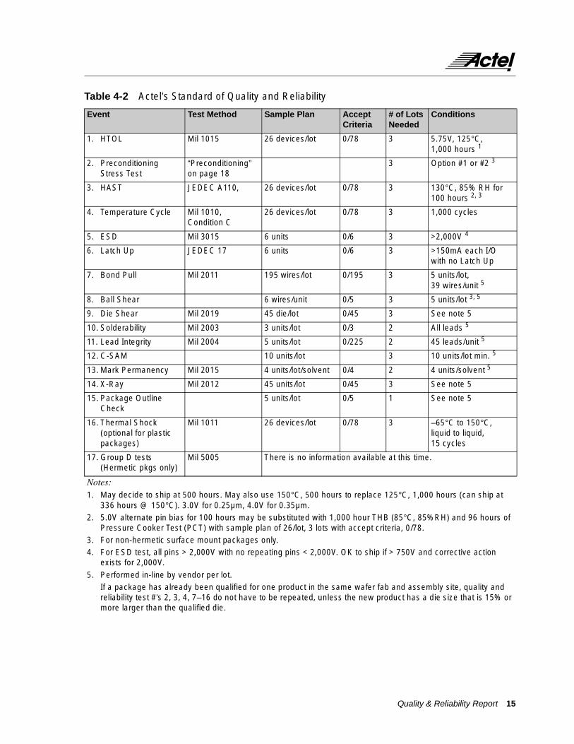
Table 4-2 Actel’s Standard of Quality and Reliability
Event Test Method Sample Plan Accept Criteria
# of Lots Needed
Conditions
1. HTOL Mil 1015 26 devices/lot 0/78 3 5.75V, 125°C, 1,000 hours 1
2. Preconditioning Stress Test
“Preconditioning” on page 18
3 Option #1 or #2 3
3. HAST JEDEC A110, 26 devices/lot 0/78 3 130°C, 85% RH for 100 hours 2, 3
4. Temperature Cycle Mil 1010, Condition C
26 devices/lot 0/78 3 1,000 cycles
5. ESD Mil 3015 6 units 0/6 3 >2,000V 4
6. Latch Up JEDEC 17 6 units 0/6 3 >150mA each I/O with no Latch Up
7. Bond Pull Mil 2011 195 wires/lot 0/195 3 5 units/lot, 39 wires/unit 5
8. Ball Shear 6 wires/unit 0/5 3 5 units/lot 3, 5
9. Die Shear Mil 2019 45 die/lot 0/45 3 See note 5
10. Solderability Mil 2003 3 units/lot 0/3 2 All leads 5
11. Lead Integrity Mil 2004 5 units/lot 0/225 2 45 leads/unit 5
12. C-SAM 10 units/lot 3 10 units/lot min. 5
13. Mark Permanency Mil 2015 4 units/lot/solvent 0/4 2 4 units/solvent 5
14. X-Ray Mil 2012 45 units/lot 0/45 3 See note 5
15. Package Outline Check
5 units/lot 0/5 1 See note 5
16. Thermal Shock(optional for plastic packages)
Mil 1011 26 devices/lot 0/78 3 –65°C to 150°C, liquid to liquid,15 cycles
17. Group D tests (Hermetic pkgs only)
Mil 5005 There is no information available at this time.
Notes:1. May decide to ship at 500 hours. May also use 150°C, 500 hours to replace 125°C, 1,000 hours (can ship at
336 hours @ 150°C). 3.0V for 0.25µm, 4.0V for 0.35µm.2. 5.0V alternate pin bias for 100 hours may be substituted with 1,000 hour THB (85°C, 85%RH) and 96 hours of
Pressure Cooker Test (PCT) with sample plan of 26/lot, 3 lots with accept criteria, 0/78.3. For non-hermetic surface mount packages only.4. For ESD test, all pins > 2,000V with no repeating pins < 2,000V. OK to ship if > 750V and corrective action
exists for 2,000V.
5. Performed in-line by vendor per lot.If a package has already been qualified for one product in the same wafer fab and assembly site, quality and reliability test #’s 2, 3, 4, 7–16 do not have to be repeated, unless the new product has a die size that is 15% or more larger than the qualified die.
Quality & Reliability Report 15

Table 4-3 Actel’s Standard Qualification Requirements for New Products
Test DescriptionNew
Product(s) New FabNew Ceramic
PackageNew Plastic
Package
1. HTOL X1 X X2
2. HAST X X1 X1
3. Temperature Cycle X X X
4. ESD X X
5. Latch Up X X
6. Bond Pull X X X
7. Ball Shear X X
8. Die Shear X X
9. Solderability X X
10. Lead Integrity X X
11. Mark Permanency X X
12. X-Ray X X
13. Preconditioning X X
14. C-SAM X X
15. Thermal Shock –Optional (Plastic) X X X
16. AC/DC Characteristics X X
17. Group D X
Notes:1. For a new product and new fab, three wafer runs are required for qualification. Before qualification is
completed, devices may be shipped as pre-production samples. Parts are believed to be good; some testing has been done. All parts must be marked “PP.” Customers are advised of part status.
2. If a package has already been qualified for one product in the same assembly site and same fab process, test #’s 2, 3, 4, 7–17 do not have to be repeated unless the new product has a die size that is 15% or more larger than the qualified die. If there are several packages within a family (same body size, lead finish, and package material), a new family member does not require qualification if:– A product within the same product family in a large die size is already qualified.– There is no change in the package body outline and the lead pitch is not smaller than this family member
being qualified.– The distance from the package edge to the die edge is less than or equal to the qualified package family
member.
16 Quality & Reliability Report
Table 4-4 Special Combination Qualification Requirements for Process and Design Changes
Test Description
New
Ass
emb
ly P
lan
t 1
& 2
New
Pkg
3 &
4
New
Lea
d F
inis
h
Ch
ang
e in
Pac
kag
ing
M
ater
ial(
s) 5
Mas
k ch
ang
es a
ffec
tin
g
die
siz
e o
r ac
tive
ele
men
t 1
Maj
or
Fab
P
roce
ss C
han
ge
1 &
6
Exi
stin
g P
kg A
lrea
dy
Qu
alif
ied
by
the
Ven
do
r 2&
5
New
Dev
ice
1. HTOL X X X
2. HAST7 X X8 X8 X8
3. Temp Cycle X X X X X X X
4. ESD X9 X9 X9
5. Latch Up X X X
6. Bond Pull X X X X
7. Ball Shear X X X X
8. Die Shear X X X X
9. Solderability X X X X X
10. Lead Plate Thickness X X X X
11. Mark Permanency X X X
12. X-Ray X X X X
13. Thermal Shock (Optional) X X X
14. C-SAM X X X X
15. AC/DC Char X X X
16. Sort, FT Yield Analysis X X X X X X X X
17. Program Yield Analysis X X X
18. High Temperature Storage X X X
19. Temperature Humidity – Unbiased 85°C/85%RH
X X X
Notes:1. Analysis is necessary. Once a wafer fab is qualified for a given die redesign change, other fabs can be qualified
by test 18 only (no additional HTOL is necessary).2. MInor Fab change qualification requires determination by the TRB.
3. Major Process Change, refer to Appendix A of MIL-PRF-38535, and MIL-STD 883.4. New packages are defined as those that have been qualified for the first time.5. The biggest package and die size for each family must be used for qualification.6. A Major Die Redesign change is defined as any change of active device size or design rules. If a mask change
is minor such as adjust CD, change E-Test structure, etc. only sort and final test yield are required.
7. May substitute 1,000 hours biased THB (85°C, 85% RH).8. One lot is required for in-house reliability testing. Use qualification and reliability data from the vendor as
supporting information.9. Only required if I/O buffer is redesigned.
Quality & Reliability Report 17

PreconditioningUse the following conditions for all PLCC, TQFP, VQFP, BGA and PQFP packages.
1. Bake packages according to the package’s dry pack baking requirement.
2. Perform C-SAM.
3. Temperature Cycle @ –55°C to 125°C for 10 cycles.
4. Bake all parts at 125°C for 12 hours.
5. Moisture soak all parts @ 30°C/60% RH for 196 hours.
6. Simulate all parts through 3 cycles of IR Reflow with the following profile1:
a. Ingress at 25°C.
b. Ramp up temperature +6°C/second maximum.
c. Temperature maintained at 125 (±25)°C for 120 seconds maximum.
d. Time above 180°C for 120–180 seconds maximum.
e. Time at maximum temperature 10–40 seconds.
f. Maximum temperature = 220 + 5°C.
g. Ramp down at 6°C/second maximum.
h. Perform C-SAM.
7. Subject parts to other reliability tests as appropriate.
Use the following conditions for RQ packages.
1. Bake all parts per the package’s dry pack baking requirement.
2. Perform C-SAM1.
3. Temperature Cycle @ –55°C to 125°C for 10 cycles.
4. Bake all parts at 125°C for 12 hours.
5. Moisture soak all parts @ 30°C/60% RH for 48 hours.
6. Simulate all parts through 3 cycles of IR Reflow with the following profile1:a. Ingress at 25°C
b. Ramp up temperature +6°C/second maximum
c. Temperature maintained at 125 (±25)°C for 120 seconds max.
d. Time above 180°C for 120–180 seconds maximum
e. Time at maximum temperature 10–40 seconds.
f. Maximum temperature = 220 + 5°C.
g. Ramp down at 6°C/second maximum
h. Perform C-SAM
7. Subject parts to other reliability tests as appropriate.
1. All temperatures refer to the top of the package and are measured on the package body surface. The devices should be allowed to cool down for a minimum of five (5) minutes between IR convection.
18 Quality & Reliability Report

5. Quality & Reliability Testing
High Temperature Operating Life (HTOL)The intent of an HTOL test is to operate a device dynamically (meaning the device is powered up with I/Os and internal nodes toggling to simulate actual system use) at a high temperature (usually 125°C or 150°C) and extrapolate the failure rate to typical operating conditions. This test is defined by Military Standard-883 in the Group C Quality Conformance Tests. The Arrhenius equation (Equation 1) is used to calculate the extrapolation:
R = R0 * exp (Ea/kT) Eq. 1
where R is the failure rate, R0 is a constant for a particular process, T is the absolute temperature in degrees Kelvin, k is Boltzmann’s constant (8.62 X 10⁻⁵ eV/°K), and Ea is the activation energy for the process in electron volts.
To determine the acceleration factor for a given failure mode at temperature T2 as compared with temperature T1, we derive from the Arrhenius equation:
A(T1, T2) = exp[(Ea/k) * (1/T1)–(1/T2)] Eq. 2
To use the Arrhenius equation, we need to know the activation energy of the failure mode. Table 5-1 gives the activation energies of typical semiconductor failure modes.
To evaluate Actel’s FPGAs, we program an actual design application into most devices (some units are burned in unprogrammed) and perform a dynamic burn-in by toggling the clock pins at 1 MHz or higher. The designs selected use 85 to 97 percent of the available logic modules and 85 to 94 percent of the I/Os. Outputs are loaded with 1.2 to 2.8k Ω resistors to VCC. Under these conditions, each unit typically draws a minimum of 100 mA during dynamic burn-in. Most of this current comes from the output loading, while about 5 mA is from the device supply current. For a 125°C burn-in, this results in junction temperatures of at least 150°C for plastic packages and 145°C for ceramic packages (depending on package type). Because junction temperatures can vary a great deal due to package, product, frequency, design, voltage, and other factors, we use the ambient temperature to calculate failure rates. These are worst case conditions because ambient temperature is always lower than junction temperature, and there is less acceleration
Table 5-1 CMOS Failure Modes
Failure Mechanism Activation Energy
Ionic Contamination 1.0 eV
Oxide Defects 0.3 eV
Hot Carrier Trapping in Oxide (Short Channels) –0.06 eV
Silicon Defects 0.5 eV
Aluminum-Silicon-Copper Electromigration 0.6 eV
Contact Electromigration 0.9 eV
Electrolytic Corrosion 0.54 eV
Quality & Reliability Report 19

when extrapolating device hours at lower temperatures. Most burn-in is done at VCC = 5.75V or VCC = 6.0V for 5.0V devices and VCC = 4.0V for 3.3V devices (for voltage acceleration of the antifuse) and 125°C or 150°C.
As mentioned previously, some units are burned in unprogrammed. To accomplish this, we use internal circuitry that allows us to take advantage of the product’s test features to shift commands to the chip serially during burn-in. All internal routing tracks are toggled between 0V and VCC. When vertical tracks are at VCC, horizontal tracks are held at 0V, and vice versa. Thus, all antifuses that can connect vertical and horizontal tracks receive a full VCC stress in both directions. These toggling vertical tracks connect to logic module inputs and outputs when a part is programmed. Finally, a command is sent to the chip to toggle some external I/O pins between 0V and VCC. This dynamic burn-in circuit is the same one used by Actel to screen unprogrammed products to MIL-STD-883 requirements. Since virtually all antifuses receive a full VCC stress, this screen is much more effective in catching unprogrammed antifuse infant mortality failures than is burning in programmed devices, as it only stresses a fraction of the antifuses.
A failure is defined as any device that shows a functional failure, exceeds data sheet DC limits, or exhibits an AC speed drift. Among the parts tested, no speed drift, faster or slower, has been observed within the accuracy of the test setup. Failure rates at 55°C, 70°C, and 90°C were extrapolated by using the Arrhenius equation and general activation energies of 0.6 eV and 0.9 eV. Poisson statistics were used to derive a calculated failure rate with a 60 percent confidence level. Poisson statistics are valid for low failure rates and failure modes occurring randomly with time. At 55°C, the calculated failure rate with a confidence level of 60 percent (0.6 eV) was 22 FITs, or 0.0022 percent failures per 1,000 hours. This number was derived from nearly nine million device hours (at 125°C) of data. There were seven total failures out of 7704 tested units representing 134 different wafer lots. There were no infant mortality failures, which would normally occur in the first 80 hours of burn-in. Six of the seven failures observed were due to common CMOS failure modes (gate oxide failure, silicon defects, or open Via). This single antifuse-related failure in nine million device hours at 125°C represents a product antifuse failure rate of significantly less than 10 FITs at 5.5V.
Table 5-2 0.25µ High Temperature Operating Life (HTOL)
Product Run # Package Units
Number of Failures (Hours)
168 500 1,000 2,000
SX32A T25J002 208 PQFP 130 0 0 – –
SX32A T25J002 208 PQFP 80 – – 0 –
20 Quality & Reliability Report
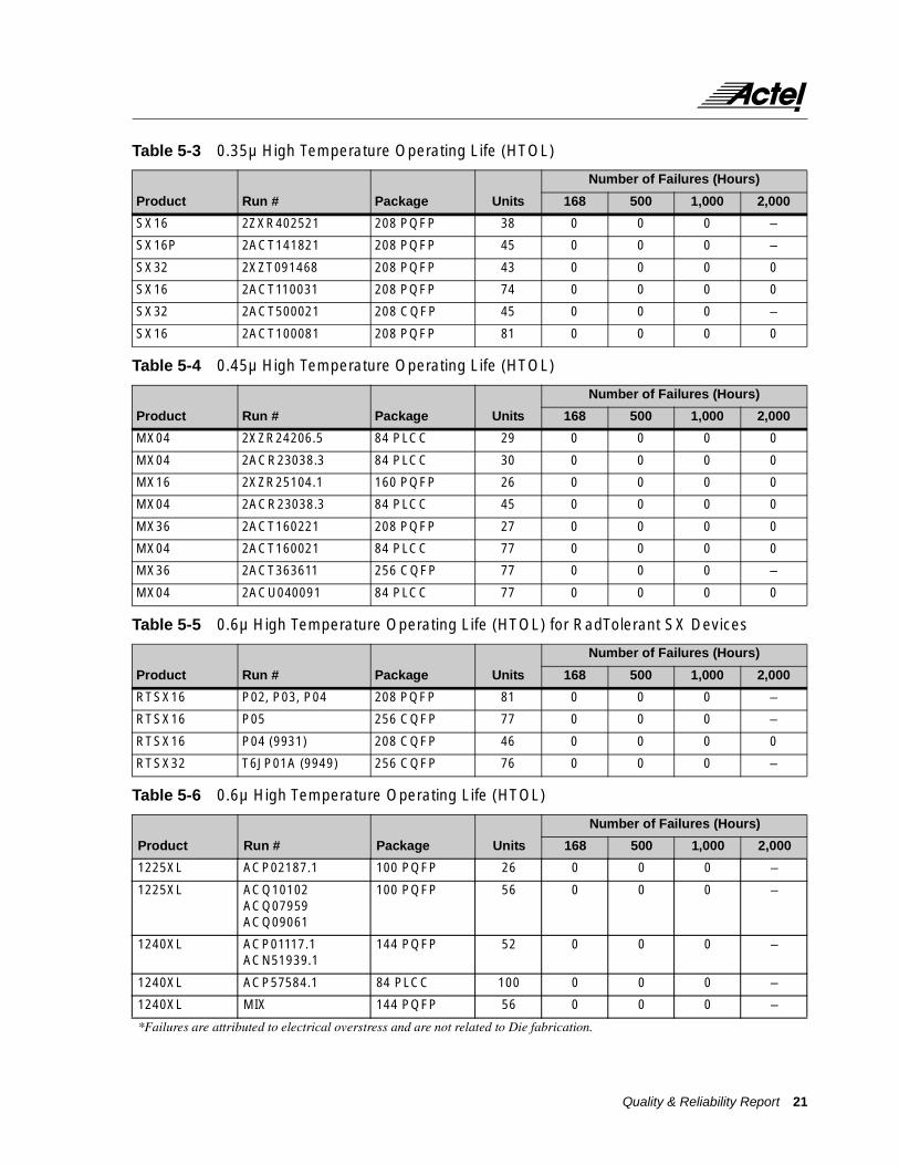
Table 5-3 0.35µ High Temperature Operating Life (HTOL)
Product Run # Package Units
Number of Failures (Hours)
168 500 1,000 2,000
SX16 2ZXR402521 208 PQFP 38 0 0 0 –
SX16P 2ACT141821 208 PQFP 45 0 0 0 –
SX32 2XZT091468 208 PQFP 43 0 0 0 0
SX16 2ACT110031 208 PQFP 74 0 0 0 0
SX32 2ACT500021 208 CQFP 45 0 0 0 –
SX16 2ACT100081 208 PQFP 81 0 0 0 0
Table 5-4 0.45µ High Temperature Operating Life (HTOL)
Product Run # Package Units
Number of Failures (Hours)
168 500 1,000 2,000
MX04 2XZR24206.5 84 PLCC 29 0 0 0 0
MX04 2ACR23038.3 84 PLCC 30 0 0 0 0
MX16 2XZR25104.1 160 PQFP 26 0 0 0 0
MX04 2ACR23038.3 84 PLCC 45 0 0 0 0
MX36 2ACT160221 208 PQFP 27 0 0 0 0
MX04 2ACT160021 84 PLCC 77 0 0 0 0
MX36 2ACT363611 256 CQFP 77 0 0 0 –
MX04 2ACU040091 84 PLCC 77 0 0 0 0
Table 5-5 0.6µ High Temperature Operating Life (HTOL) for RadTolerant SX Devices
Product Run # Package Units
Number of Failures (Hours)
168 500 1,000 2,000
RTSX16 P02, P03, P04 208 PQFP 81 0 0 0 –
RTSX16 P05 256 CQFP 77 0 0 0 –
RTSX16 P04 (9931) 208 CQFP 46 0 0 0 0
RTSX32 T6JP01A (9949) 256 CQFP 76 0 0 0 –
Table 5-6 0.6µ High Temperature Operating Life (HTOL)
Product Run # Package Units
Number of Failures (Hours)
168 500 1,000 2,000
1225XL ACP02187.1 100 PQFP 26 0 0 0 –
1225XL ACQ10102ACQ07959ACQ09061
100 PQFP 56 0 0 0 –
1240XL ACP01117.1ACN51939.1
144 PQFP 52 0 0 0 –
1240XL ACP57584.1 84 PLCC 100 0 0 0 –
1240XL MIX 144 PQFP 56 0 0 0 –
*Failures are attributed to electrical overstress and are not related to Die fabrication.
Quality & Reliability Report 21

1280XL ACP212072ACP19329.1
160 PQFP 76 0 0 0 –
1280XL MIX 84 PLCC 100 0 0 0 –
3265DX ACP163684 160 PQFP 78 0 0 0 –
A1415 ACP17300 100 PQFP 100 0 0 0 –
A1425 ACP122761 100 PQFP 100 0 0 0 –
A1425 ACP12285ACP34166ACP27991
100 PQFP 88 0 0 0 –
1460BP 2543054025430550
208 PQFP 52 0 0 0 –
14100BP 26026670 208 RQFP 27 0 0 0 –
32140DX ACP33277.1ACP55730.1ACP54023.1
208 PQFP 75 0 0 0 –
32140DX ACP56255.1ACP56254.1
208 PQFP 52 0 0 0 –
32140DX ACP540231ACP56254.1
160 PQFP 26 0 0 0 –
32140DX 25464510 160 PQFP 26 0 0 0 –
32200DX 26207340 208 PQFP 29 0 0 0 –
32140DX ACP562551 208 PQFP 28 0 – 0 0
1415A ACP17300 100 PQFP 101 0 – 0 0
32300DX ACQ09069.1 240 RQFP 26 0 – 2* 0
A1425A(150°C)
UCJ01,02,03 133 PGA 130 – 0 – –
A32100DX(150°C)
ACR50293.1 84 CQFP 80 – 0 – –
32140DX G10854 208C PQFP 26 0 0 0 –
1280XL ACR53214 160 PQFP 129 0 – – –
A1240XL ACR50594.1 144C PQFP 228 0 – – –
A1240XL ACR50594.1 144C PQFP 143 0 – – –
A1240XL ACR50594.1 144C PQFP 227 0 – – –
A1280XL ACT10293.1 172 CQFP 80 0 0 0 –
A32200DX ACT166851 256 CQFP 77 0 0 0 –
A1280XL ACU166851 176 PGA 76 0 0 0 –
Table 5-6 0.6µ High Temperature Operating Life (HTOL) (Continued)
Product Run # Package Units
Number of Failures (Hours)
168 500 1,000 2,000
*Failures are attributed to electrical overstress and are not related to Die fabrication.
22 Quality & Reliability Report

Table 5-7 0.8µ High Temperature Operating Life (HTOL)
Product Run # Package Units
Number of Failures (Hours)
168 500 1,000
1280XL 244644302444262024381610
160 PQFP 78 1 0 0
1425 JK08, 09,10 133 PGA 140 0 0 0
1425 JK08, 09,10 84 PLCC 135 0 0 0
1425A UCJ01, 2, 3 133 PGA 130 0 0 0
1425A ACN32804ACN30805ACN33807
133 PGA 130 0 0 0
A1425 UCJ013 100 PQFP 100 0 0 0
1440A JN05 100 VQFP 79 0 0 0
1440A 51940.1 100 VQFP 79 0 0 0
1460A JL-01 208 PQFP 80 0 0 0
1460A JL-01 207 PGA 80 0 0 0
1460A JL-03 208 PQFP 62 0 0 0
1460A JL-06B 207 PGA 65 0 0 0
1460A PC435091PC435092PC435093
207 PGA207 PGA207 PGA
80 0 0 0
14100A 24239130UCLO1
208 RQFP208 RQFP
5125
00
00
00
14100A 25290820 313 PBGA 45 0 0 0
A1460A(150°C)
UCKT01 207 CPGA 81 0 – –
A32100DX 84 CQFP 80 – – –
A14100A UCL049 256 CQFP 15 – – 0
A1460A (150°C, 184 hrs)
UCK056 207B PGA 80 0 – –
1280XL (150°C, 184 hrs)
ACT10293.1 721 CQFP 80 0 – –
RT14100A UCL055 256E CQFP 18 – – 0
A14100A(150°C, 184 hrs)
UCL058 256E CQFP 82 0 – –
Quality & Reliability Report 23

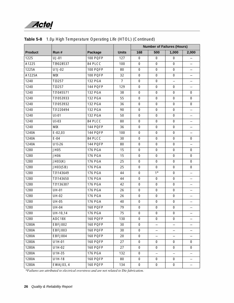
Table 5-8 1.0µ High Temperature Operating Life (HTOL)
Product Run # Package Units
Number of Failures (Hours)
168 500 1,000 2,000
1010A JG03 68 PLCC 59 0 0 0 0
1010A JG03 68 PLCC 117 0 0 0 0
1010A TI24 68 PLCC 74 0 0 0 0
1010A TI1104TI1243TI1263TI1297
68 PLCC 107 0 0 0 –
1010A E01-1 68 PLCC 69 0 0 0 –
1010A E02-1 68 PLCC 70 0 0 0 –
1010B TI2072857TI2072858TI2072860
68 PLCC 400 1* 0 0 –
1010B U1G-01 68 PLCC 79 0 0 0 –
1010B U1G-02 68 PLCC 57 0 0 – –
1010B U9G01P 100 PQFP 76 0 0 0 –
1020A JF01 84 PLCC 25 0 0 0 0
1020A JF01 84 PLCC 15 0 0 0 0
1020A JF02 84 PLCC 44 0 0 0 0
1020A JF02 84 PLCC 41 0 0 0 0
1020A JF04 84 PLCC 77 0 0 0 –
1020A JF04 84 PLCC 20 0 0 – –
1020A JF14 84 PLCC 58 0 0 – –
1020A JF14 84 PLCC 100 0 1* – –
1020A JF37 84 PLCC 14 1* – – –
1020A JF37 84 PLCC 20 0 – – –
1020A JF39 84 PLCC 32 0 – – –
1020A JF39 84 PLCC 29 0 – – –
1020A JF42 84 PLCC 49 0 0 – –
1020A JF42 84 PLCC 30 0 1* – –
1020A JF66 84 PLCC 33 0 0 0 –
1020A JF66 84 PLCC 39 0 0 0 –
1020A JF67 84 PLCC 49 0 0 0 –
1020A JF67 84 PLCC 45 0 0 0 –
1020A TI S#1 84 PLCC 79 0 0 0 –
1020A E-14 84 PLCC 45 0 0 0 0
1020A E-15 84 PLCC 44 0 0 0 0
1020A E-17 84 PLCC 45 0 0 0 0
1020A JF-207 100 PQFP 129 0 0 0 –
*Failures are attributed to electrical overstress and are not related to Die fabrication.
24 Quality & Reliability Report

1020A D1J1815D2B2704
84 PGA 51 0 0 0 –
1020A E-01 84 PLCC 45 0 0 0 –
1020A E-02 84 PLCC 45 0 0 0 –
1020A E-03 84 PLCC 45 0 0 0 –
1020A ADK29X 84 PLCC 45 0 0 0 0
1020A ADA72X 84 PLCC 45 0 0 0 0
1020A ADC21X 84 PLCC 45 0 0 0 0
1020A TI1130 84 PLCC 223 0 0 0 –
1020A TI1800 84 PLCC 34 0 0 – –
1020A UP-04UP-05
84 PLCC84 PLCC
4040
00
00
00
––
1010B TI5276893 84 PLCC 100 0 0 0 –
1020B JJ-14 84 PLCC 45 0 0 0 –
1020B JJ-15 84 PLCC 45 0 0 0 –
1020B JJ-17 84 PLCC 45 0 0 0 –
1020B JJ-13 84 PGA 30 0 0 0 –
1020B JJ-13 84 PGA 80 0 0 – –
1020B JJ-16 84 PLCC 80 0 0 0 –
1020B U1P-01 84 PLCC 40 0 0 0 –
1020B U1P-02 84 PLCC 40 0 0 0 –
1020B JJ-24 84 PLCC 87 0 0 0 –
1020B EBFJ001 84 PLCC 40 0 0 0 –
1020B EBFI004 84 PLCC 40 0 0 0 –
1020B U1P41HM 100 PQFP 80 0 0 0 –
1020B U1P25 80 VQFP 45 0 0 – –
1020B U1P83U1P25
80 VQFP80 VQFP
4339
00
00
00
–
1020B U1P05 100 PQFP 129 0 0 0 –
1020B U1P209B 84 PLCC 40 0 0 0 –
1020B U9P01U9P021A
100 PQFP100 PQFP
133 0 1* 0 –
1020B U9P-004 84 PLCC 47 0 0 0 –
1020B U9P046 84 PLCC 100 0 0 0 –
1020B 6085878 84 PLCC 100 0 0 0 –
1020B U9P128 84 PLCC 100 0 0 0 –
1020B UP121 84 CQFP 24 0 0 0 –
1225 UJ-01 100 PGA 80 0 0 0 –
Table 5-8 1.0µ High Temperature Operating Life (HTOL) (Continued)
Product Run # Package Units
Number of Failures (Hours)
168 500 1,000 2,000
*Failures are attributed to electrical overstress and are not related to Die fabrication.
Quality & Reliability Report 25
1225 UJ-01 100 PQFP 127 0 0 0 –
A1225 TI9028537 84 PLCC 100 0 0 0 –
1225A U1J-02 100 PQFP 80 0 0 0 –
A1225A MIX 100 PQFP 32 0 0 0 –
1240 TI3257 132 PGA 7 0 0 – –
1240 TI3257 144 PQFP 129 0 0 0 –
1240 TI1045571 132 PGA 38 0 0 0 0
1240 TI1053933 132 PGA 55 0 0 0 0
1240 TI1053932 132 PGA 36 0 0 0 0
1240 TI1220494 132 PGA 90 0 0 0 –
1240 UI-01 132 PGA 50 0 0 0 –
1240 UI-03 84 PLCC 80 0 0 0 –
1240 MIX 144 PQFP 36 0 0 0 –
1240A E-02,03 144 PQFP 100 0 0 0 –
1240A E-04 84 PLCC 30 0 0 0 0
1240A U1I-26 144 PQFP 80 0 0 0 –
1280 JH05 176 PGA 15 0 0 0 0
1280 JH06 176 PGA 15 0 0 0 0
1280 JH03(K) 176 PGA 25 0 0 0 0
1280 JH03(SB) 176 PGA 25 0 0 0 0
1280 TI1143649 176 PGA 44 0 1* 0 –
1280 TI1143650 176 PGA 44 0 0 0 –
1280 TI1136307 176 PGA 42 0 0 0 –
1280 UH-01 176 PGA 26 0 0 0 –
1280 UH-02 176 PGA 26 0 0 0 –
1280 UH-05 176 PGA 40 0 0 0 –
1280 UH-04 160 PQFP 79 0 0 0 –
1280 UH-10,14 176 PGA 75 0 0 0 –
1280 ADC18X 160 PQFP 130 0 0 0 –
1280A EBFJ002 160 PQFP 30 0 – – –
1280A EBFJ003 160 PQFP 30 0 – – –
1280A EBFJ004 160 PQFP 20 0 – – –
1280A U1H-01 160 PQFP 27 0 0 0 0
1280A U1H-02 160 PQFP 27 0 0 0 0
1280A U1H-35 176 PGA 132 0 – – –
1280A U1H-18 160 PQFP 80 0 0 0 –
1280A EWAJ03, 4 160 PQFP 134 0 0 0 –
Table 5-8 1.0µ High Temperature Operating Life (HTOL) (Continued)
Product Run # Package Units
Number of Failures (Hours)
168 500 1,000 2,000
*Failures are attributed to electrical overstress and are not related to Die fabrication.
26 Quality & Reliability Report

1280A U1H25, 29 84 PLCC 79 0 0 0 –
1280A U1H235/6 160 PQFP 80 0 0 0 –
A1020B 103501 84PLCC 124 0 0 0 –
A1020A UP121 84E CQFP 24 0 0 0 –
A1280A U1H486 172B CQFP 81 0 0 0 –
Lots Accelerated at 150°C
Product Run # Package Units
Number of Failures (Hours)
184 500 1,000
A1280A U1H83 172 CQFP 45 – 0
A1280A U1H363 172 CQFP 58 0 – –
A1280A U1H442 176B PGA 81 0 – –
A1020A U1RT01 84B CQFP 80 – 0 –
A1280A UIH439 172 CQFP 18 0 – –
A1280A U1H439 172 CQFP 310 0 – –
A1020 U1RT02 84E CQFP 699 0 – –
A1280A U1H551 176 PGA 77 0 – –
Table 5-8 1.0µ High Temperature Operating Life (HTOL) (Continued)
Product Run # Package Units
Number of Failures (Hours)
168 500 1,000 2,000
*Failures are attributed to electrical overstress and are not related to Die fabrication.
Quality & Reliability Report 27
Highly Accelerated Stress Test (HAST)
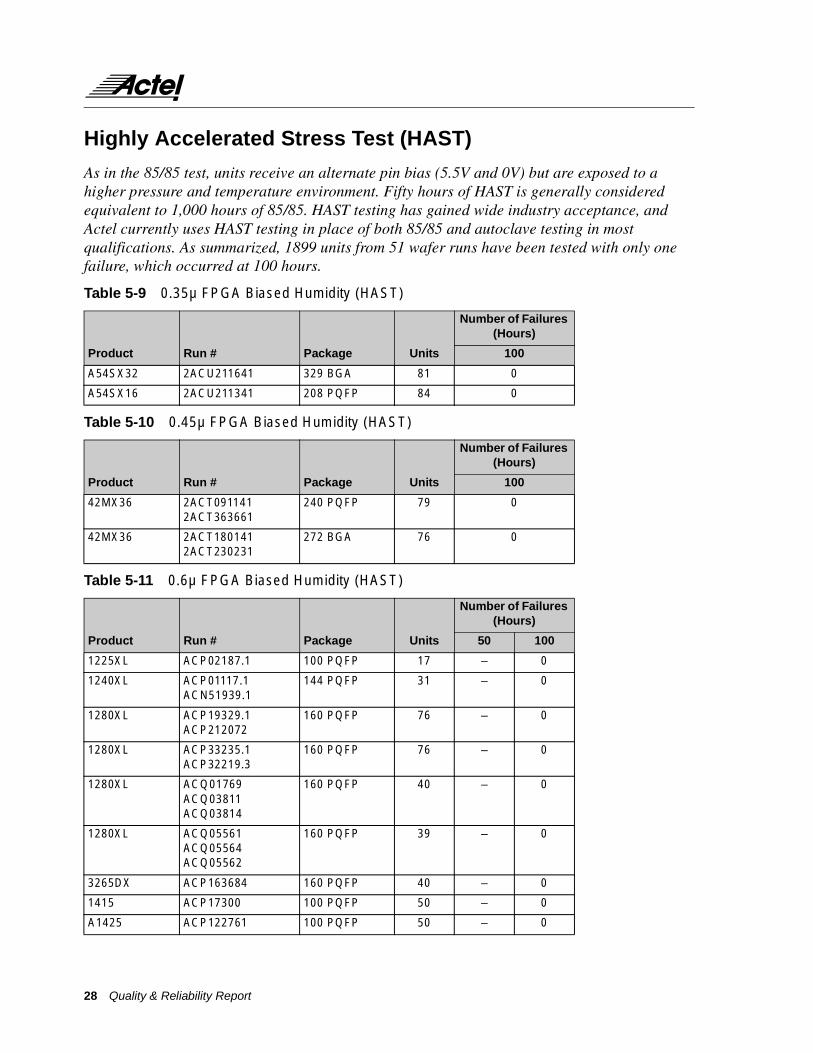
As in the 85/85 test, units receive an alternate pin bias (5.5V and 0V) but are exposed to a higher pressure and temperature environment. Fifty hours of HAST is generally considered equivalent to 1,000 hours of 85/85. HAST testing has gained wide industry acceptance, and Actel currently uses HAST testing in place of both 85/85 and autoclave testing in most qualifications. As summarized, 1899 units from 51 wafer runs have been tested with only one failure, which occurred at 100 hours.
Table 5-9 0.35µ FPGA Biased Humidity (HAST)
Product Run # Package Units
Number of Failures (Hours)
100
A54SX32 2ACU211641 329 BGA 81 0
A54SX16 2ACU211341 208 PQFP 84 0
Table 5-10 0.45µ FPGA Biased Humidity (HAST)
Product Run # Package Units
Number of Failures (Hours)
100
42MX36 2ACT091141 2ACT363661
240 PQFP 79 0
42MX36 2ACT180141 2ACT230231
272 BGA 76 0
Table 5-11 0.6µ FPGA Biased Humidity (HAST)
Product Run # Package Units
Number of Failures (Hours)
50 100
1225XL ACP02187.1 100 PQFP 17 – 0
1240XL ACP01117.1ACN51939.1
144 PQFP 31 – 0
1280XL ACP19329.1ACP212072
160 PQFP 76 – 0
1280XL ACP33235.1ACP32219.3
160 PQFP 76 – 0
1280XL ACQ01769ACQ03811ACQ03814
160 PQFP 40 – 0
1280XL ACQ05561ACQ05564ACQ05562
160 PQFP 39 – 0
3265DX ACP163684 160 PQFP 40 – 0
1415 ACP17300 100 PQFP 50 – 0
A1425 ACP122761 100 PQFP 50 – 0
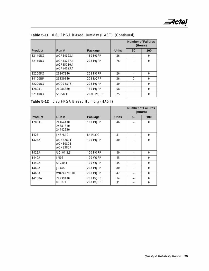
28 Quality & Reliability Report
32140DX ACP54023.1 160 PQFP 26 – 0
32140DX ACP33277.1ACP55730.1ACP54023.1
208 PQFP 76 – 0
32200DX 26207340 208 PQFP 26 – 0
14100BP 26330340 208 RQFP 26 0 0
32200DX ACQ03818.1 208 PQFP 30 – 0
1280XL 26084380 160 PQFP 58 – 0
32140DX 55558.1 208C PQFP 25 0
Table 5-12 0.8µ FPGA Biased Humidity (HAST)
Product Run # Package Units
Number of Failures (Hours)
50 100
1280XL 244644302438161024442620
160 PQFP 46 – 0
1425 JK8,9,10 84 PLCC 81 – 0
1425A ACN32804ACN30805ACN33807
100 PQFP 80 – 0
1425A UCJ01,2,3 100 PQFP 80 – 0
1440A JN05 100 VQFP 45 – 0
1440A 51940.1 100 VQFP 45 – 0
1460A JL04A 208 PQFP 80 – 0
1460A WB24279010 208 PQFP 47 – 0
14100A 24239130UCLO1
208 RQFP208 RQFP
1431
––
00
Table 5-11 0.6µ FPGA Biased Humidity (HAST) (Continued)
Product Run # Package Units
Number of Failures (Hours)
50 100
Quality & Reliability Report 29
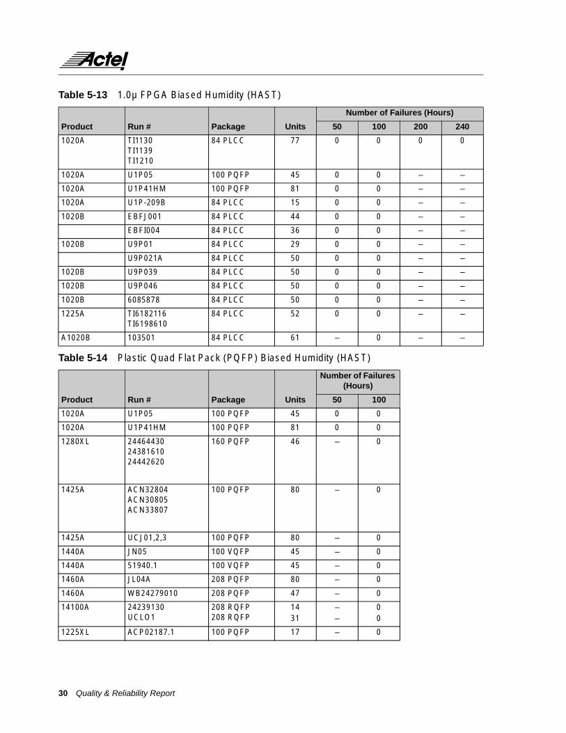
Table 5-13 1.0µ FPGA Biased Humidity (HAST)
Product Run # Package Units
Number of Failures (Hours)
50 100 200 240
1020A TI1130TI1139TI1210
84 PLCC 77 0 0 0 0
1020A U1P05 100 PQFP 45 0 0 – –
1020A U1P41HM 100 PQFP 81 0 0 – –
1020A U1P-209B 84 PLCC 15 0 0 – –
1020B EBFJ001 84 PLCC 44 0 0 – –
EBFI004 84 PLCC 36 0 0 – –
1020B U9P01 84 PLCC 29 0 0 – –
U9P021A 84 PLCC 50 0 0 – –
1020B U9P039 84 PLCC 50 0 0 – –
1020B U9P046 84 PLCC 50 0 0 – –
1020B 6085878 84 PLCC 50 0 0 – –
1225A TI6182116TI6198610
84 PLCC 52 0 0 – –
A1020B 103501 84 PLCC 61 – 0 – –
Table 5-14 Plastic Quad Flat Pack (PQFP) Biased Humidity (HAST)
Product Run # Package Units
Number of Failures (Hours)
50 100
1020A U1P05 100 PQFP 45 0 0
1020A U1P41HM 100 PQFP 81 0 0
1280XL 244644302438161024442620
160 PQFP 46 – 0
1425A ACN32804ACN30805ACN33807
100 PQFP 80 – 0
1425A UCJ01,2,3 100 PQFP 80 – 0
1440A JN05 100 VQFP 45 – 0
1440A 51940.1 100 VQFP 45 – 0
1460A JL04A 208 PQFP 80 – 0
1460A WB24279010 208 PQFP 47 – 0
14100A 24239130UCLO1
208 RQFP208 RQFP
1431
––
00
1225XL ACP02187.1 100 PQFP 17 – 0
30 Quality & Reliability Report

1240XL ACP01117.1ACN51939.1ACP212072.2
144 PQFP 31 – 0
1280XL ACP19329.1 160 PQFP 76 – 0
1280XL ACP33235.1 ACP32219.3
160 PQFP 76 – 0
3265DX ACP163684 160 PQFP 40 – 0
1415 ACP17300 100 PQFP 50 – 0
A1425 ACP122761 100 PQFP 50 – 0
1280XL ACQ01769 ACQ03811 ACQ03814
160 PQFP 40 – 0
1280XL ACQ05561
ACQ05564
ACQ05562
160 PQFP 39 – 0
1460BP 25430540
25430550
208 PQFP 52 – 0
14100BP 26330340 208 RQFP 26 – 0
32140DX ACP33277.1 ACP55730.1 ACP54023.1
208TE PQFP 76 – 0
32200DX 26207340 208 PQFP 26 – 0
32200DX 26207340 208 PQFP 24 0 0
14100BP 26330340 208 RQFP 26 0 0
32200DX ACQ03818.1 208 PQFP 30 – 0
1280XL 26084380 160 PQFP 58 – 0
Table 5-14 Plastic Quad Flat Pack (PQFP) Biased Humidity (HAST) (Continued)
Product Run # Package Units
Number of Failures (Hours)
50 100
Quality & Reliability Report 31

Table 5-15 Plastic Leaded Chip Carrier (PLCC) Biased Humidity (HAST)
Product Run # Package Units
Number of Failures (Hours)
50 100
1020A TI1130TI1139TI1210
84 PLCC 77 0 0
1020A U1P-209B 84 PLCC 15 0 0
1020B EBFJ001 84 PLCC 44 0 0
1020B EBFI004 84 PLCC 36 0 0
1020B U9P01 84 PLCC 29 0 0
1020B U9P021A 84 PLCC 50 0 0
1020B U9P039 84 PLCC 50 0 0
1020B U9P046 84 PLCC 50 0 0
1020B 6085878 84 PLCC 50 0 0
1425 JK8,9,10 84 PLCC 81 – 0
1020B U9P046 84 PLCC 50 – 0
1020B 6085878 84 PLCC 50 – 0
1240A TI 0094895/6TI 00113137TI 0013142
84 PLCC 48 – 0
32 Quality & Reliability Report

Temperature Cycling/Thermal Shock
These tests check for package integrity by cycling units through temperature extremes. Data was taken for cycles of 0°C to 125°C, –40°C to 125°C, and –65°C to 150°C. Both programmed and unprogrammed units were placed on temperature cycles.
Table 5-16 Plastic Quad Flat Pack (PQFP) Temperature Cycle
Product Run # Package Units
Number of Failures (Hours)
200 500 1,000
Temperature Cycle: –55°C to 125°C
32104DX ACQ07975ACQ06716
208 TQFP 31 0 0 0
32140DX ACQ05572ACQ09703
160 TQFP 16 0 0 0
1460A 2641,0001 208 PQFP 80 0 0 0
1010B U9G042 100 PQFP 25 – 0 0
Temperature Cycle: –65°C to 150°C
1020A JF-71 100 PQFP 129 0 0 0
1020B U1P41HM 100 PQFP 80 0 0 0
1020B U1P05 100 PQFP 80 0 0 0
1280XL 25026540 176 TQFP 17 – 0 0
1280XL 2531250025312480
160 PQFP160 PQFP
76 0 0 0
1280XL 2531250025312480
160 PQFP160 PQFP
76 0 0 –
1280XL 2531250025312480
160 PQFP160 PQFP
75 0 0 0
1280XL 2531250025312480
160 PQFP160 PQFP
75 0 0 0
1280XL 2531250025312480
160 PQFP160 PQFP
74 0 0 0
1280XL 2531250025312480
160 PQFP160 PQFP
76 0 0 0
1425A UCJ01,2,3 100 PQFP 80 0 0 0
1425A ACN32804ACN30805ACN33807
100 PQFP 80 0 0 0
1440A JN-02 160 PQFP 80 0 0 0
1440A JN-05 100 VQFP 80 0 0 1
1440A 51940.1 100 VQFP 45 0 0 0
1460A JL-01 208 PQFP 80 0 0 0
1460A 25364430 208 PQFP 45 0 0 0
14100A 24239130UCLO1
208 RQFP208 RQFP
1431
––
––
00
Quality & Reliability Report 33

14100A 2537198025364960
208 RQFP208 RQFP
19 0 – –
14100A 26026670 208 RQFP 26 0 0 0
1225XL ACP02187.1 100 PQFP 18 – 0 0
1240XL ACP01117.1ACN51939.1
144 PQFP 30 – 0 0
1280XL ACP19329.1ACP212072.2
160 PQFP160 PQFP
3838
00
00
00
1280XL ACP33235.1 ACP32219.3
160 PQFP 76 0 0 0
3265DX ACP163684 160 PQFP 45 0 0 0
1440A 51940.1 100 VQFP 45 0 0 0
1415A ACP212001 100 VQFP 50 0 0 0
1415A ACP17300 100 PQFP 50 0 0 0
1460BP 2543054025430550
208 PQFP 52 0 0 0
14100BP 26330340 208 RQFP 26 0 0 0
32200DX 26207340 208TE PQFP 26 0 0 0
32140DX ACP33277.1 ACP55730.1 ACP54023.1
208TE PQFP 76 0 0 0
32140DX 26231860 208 PQFP 40 0 0 0
32140DX 26145020 208 PQFP 40 0 0 0
1460BP 26232850 208 PQFP 40 0 – –
32410DX 26272490 208 PQFP 38 0 – –
32410DX 26026660 208 PQFP 52 0 0 0
32200DX 26207340 208 PQFP 48 0 0 0
32410DX 26073180 208 PQFP 39 0 0 0
A54SX16 2ACU2413412ACU4200722ACU2224488
208 PQFP 93 0 0 0
Table 5-16 Plastic Quad Flat Pack (PQFP) Temperature Cycle (Continued)
Product Run # Package Units
Number of Failures (Hours)
200 500 1,000
34 Quality & Reliability Report

Table 5-17 Plastic Leaded Chip Carrier (PLCC) Temperature Cycle
Product Run # Package Units
Number of Failures (Hours)
100 500 1,000 2,000
Temperature Cycle: 0°C to 125°C
1010A TI15 68 PLCC 125 0 0 0 –
1010A TI24 68 PLCC 176 0 0 0 –
1010A TI1104TI1243TI1263TI1297
68 PLCC 129 0 0 0 0
1020A TI1800TI1859TI2156
84 PLCC 129 0 0 0 0
Temperature Cycle: –40°C to 125°C
1010A TI1104TI1243TI1263TI1297
68 PLCC 129 0 0 0 0
1020A TI1800TI1859TI2156
84 PLCC 129 0 0 0 0
Temperature Cycle: –55°C to 125°C
1020B U9P186U9P200
84 PLCC 30 0 0 0 –
1225XL ACQ-MIX 84 PLCC 39 0 0 0 –
Temperature Cycle: –65°C to 150°C
1020A JF-71 100 PQFP 129 0 0 0 –
1010A TI1104TI1243TI1263TI1297
68 PLCC 129 0 0 0 0
1010B TI2072857TI2072858TI2072860
68 PLCC 201 0 0 0 –
1010B U1G-01,02 68 PLCC 40 0 0 0 –
1020A TI1800TI1859TI2156
84 PLCC 129 0 0 0 0
1020A E01E02E03
84 PLCC 85 0 0 0 –
1020A S-1702A,B,C 84 PLCC 144 0 0 0 –
1020B JJ14-17 84 PLCC 81 0 0 0 –
1020B U1P-01,02 84 PLCC 40 0 0 0 –
1020B EBFJ001 84 PLCC 80 0 0 0 –
1020B EWAI003 84 PLCC 80 0 0 0 –
Quality & Reliability Report 35

1020B U1P-209B 84 PLCC 15 0 0 0 –
1020B U9P021A 84 PLCC 55 0 0 0 –
1020B U9P01 84 PLCC 23 0 0 0 –
1020B U9P039 84 PLCC 50 0 0 0 –
1020B U9P046 84 PLCC 50 0 0 0 –
1020B 6085878 84 PLCC 50 0 0 0 –
1425 JK8,9,10 84 PLCC 83 0 0 0 –
1240A TI 0113140/1TI 0094898/9TI 0094889
84 PLCC 56 0 0 0 –
A1240A TI6163513TI6163521TI6163522
84 PLCC 40 0 0 0 –
A1225A TI9039849TI6182117
84 PLCC 16 0 0 0 –
Table 5-18 0.45µ FPGA Temperature Cycle
Product Run # Package Units
Number of Failures (Hours)
100
–55°C to 150°C
42MX36 2ACT091141, 2ACT363661
240 PQFP 79 0
42MX36 2ACT180141, 2ACT230231
272 BGA 76 0
Table 5-17 Plastic Leaded Chip Carrier (PLCC) Temperature Cycle (Continued)
Product Run # Package Units
Number of Failures (Hours)
100 500 1,000 2,000
36 Quality & Reliability Report

Table 5-19 0.6µ FPGA Temperature Cycle
Product Run # Package Units
Number of Failures (Hours)
200 500 1,000
–55°C to 125°C
1225XL MIX 84 PLCC 39 0 0 0
32140DX ACQ07975ACQ06716
208TE PQFP 31 0 0 0
32140DX ACQ05572ACQ09703
160TE PQFP 16 0 0 0
1225XL ACP02187.1 100 PQFP 18 – 0 0
1240XL ACP01117.1ACN51939.1
144 PQFP 30 – 0 0
1280XL ACP19329.1ACP212072
160 PQFP160 PQFP
3838
00
00
00
3265DX ACP163684 160 PQFP 45 0 0 0
1440A 51940.1 100 VQFP 45 0 0 0
A1415 ACP212001 100 VQFP 50 0 0 0
A1415 ACP17300 100 PQFP 50 0 0 0
A14100 26026670 208 RQFP 26 0 0 0
1460BP 2543054025430550
208 PQFP 52 0 0 0
14100BP 2602667026330340
208 RQFP 45 0 0 0
32140DX ACP54023.1 160 PQFP 26 0 0 0
32140DX ACP33277.1ACP55730.1ACP54023.1
208 PQFP 76 0 0 0
32200DX 26207340 208 PQFP 26 0 0 0
–65°C to 150°C
32140DX 2623860 208 PQFP 40 0 0 0
32140DX 26145020 208 PQFP 40 0 0 0
1460BP 26247840 208 PQFP 40 0 – –
1460BP 26232850 208 PQFP 40 0 – –
32410DX 26272490 208 PQFP 38 0 – –
32410DX 26026660 208 PQFP 52 0 0 0
32200DX 26207340 208 PQFP 48 0 0 0
32410DX 26073180 208 PQFP 39 0 0 0
32410DX 26090100 208 PQFP 26 0 0 0
1460BP 26465100 208 PQFP 59 0 0 0
32300DX ACQ09705.1 204 RQFP 25 0 0 0
32140DX 266026660 208 PQFP 35 0 0 0
32140DX 266026660A 208 PQFP 78 0 0 –
1280XL 25026540 176 TQFP 17 – 0 0
Quality & Reliability Report 37
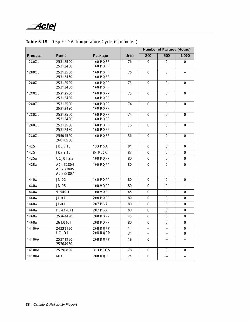
1280XL 2531250025312480
160 PQFP160 PQFP
76 0 0 0
1280XL 2531250025312480
160 PQFP160 PQFP
76 0 0 –
1280XL 2531250025312480
160 PQFP160 PQFP
75 0 0 0
1280XL 2531250025312480
160 PQFP160 PQFP
75 0 0 0
1280XL 2531250025312480
160 PQFP160 PQFP
74 0 0 0
1280XL 2531250025312480
160 PQFP160 PQFP
74 0 0 0
1280XL 2531250025312480
160 PQFP160 PQFP
76 0 0 0
1280XL 2550456026010580
160 PQFP 36 0 0 0
1425 JK8,9,10 133 PGA 81 0 0 0
1425 JK8,9,10 84 PLCC 83 0 0 0
1425A UCJ01,2,3 100 PQFP 80 0 0 0
1425A ACN32804ACN30805ACN33807
100 PQFP 80 0 0 0
1440A JN-02 160 PQFP 80 0 0 0
1440A JN-05 100 VQFP 80 0 0 1
1440A 51940.1 100 VQFP 45 0 0 0
1460A JL-01 208 PQFP 80 0 0 0
1460A JL-01 207 PGA 80 0 0 0
1460A PC435091 207 PGA 80 0 0 0
1460A 25364430 208 PQFP 45 0 0 0
1460A 261,0001 208 PQFP 80 0 0 0
14100A 24239130UCLO1
208 RQFP208 RQFP
1431
––
––
00
14100A 2537198025364960
208 RQFP 19 0 – –
14100A 25290820 313 PBGA 78 0 0 0
14100A MIX 208 RQC 24 0 – –
Table 5-19 0.6µ FPGA Temperature Cycle (Continued)
Product Run # Package Units
Number of Failures (Hours)
200 500 1,000
38 Quality & Reliability Report

Table 5-20 1.0µ FPGA Temperature Cycle
Product Run # Package Units
Number of Failures (Hours)
100 500 1,000 2,000
–0°C to 125°C
1010A TI15 68 PLCC 125 0 0 0 –
1010A TI24 68 PLCC 176 0 0 0 –
1010A TI1104TI1243TI1263TI1297
68 PLCC 129 0 0 0 0
1020A TI1800TI1859TI2156
84 PLCC 129 0 0 0 0
–40°C to 125°C
1010A TI1104TI1243TI1263TI1297
68 PLCC 129 0 0 0 0
1020A TI1800TI1859TI2156
84 PLCC 129 0 0 0 0
–55°C to 125°C
1020B U9P186
U9P200
68 PLCC 30 0 0 0
1020B U9G042 100 PQFP 25 0 0 0
–65°C to 150°C
1010A TI1104TI1243TI1263TI1297
68 PLCC 129 0 0 0 0
1010B TI2072857TI2072858TI2072860
68 PLCC 201 0 0 0 –
1010B U1G-01,02 68 PLCC 40 0 0 0 –
1020A TI1800TI1859TI2156
84 PLCC 129 0 0 0 0
1020A JF-71 100 PQFP 129 0 0 0 –
1020A E01E02E03
84 PLCC 85 0 0 0 –
1020A S-1702A,B,C 84 PLCC 144 0 0 0 –
1020B JJ14-17 84 PLCC 81 0 0 0 –
1020B U1P-01,02 84 PLCC 40 0 0 0 –
1020B EBFJ001 84 PLCC 80 0 0 0 –
1020B U1P41HM 100 PQFP 80 0 0 0 –
Quality & Reliability Report 39

1020B EWAI003 84 PLCC 80 0 0 0 –
1020B U1P-209B 84 PLCC 15 0 0 0 –
1020B U1P05 100 PQFP 80 0 0 0 –
1020B U9P021AU9P01
84 PLCC 5523
00
00
00
––
1020B U9P039 84 PLCC 50 0 0 0 –
1020B U9P046 84 PLCC 50 0 0 0 –
1020B 6085878 84 PLCC 50 0 0 0 –
A1225A TI9039849TI6182117
84 PLCC 16 0 0 0 –
A1240A TI0094901TI0081338TI0113145
144 PQFP 36 0 0 0 –
A1020B 103501 84 PLCC 62 0 – 0 –
A1240A TI6163513TI6163521TI6163522
84 PLCC 40 0 0 0 –
Table 5-20 1.0µ FPGA Temperature Cycle (Continued)
Product Run # Package Units
Number of Failures (Hours)
100 500 1,000 2,000
40 Quality & Reliability Report

Electrostatic Discharge (ESD)
Causes of ESDElectrostatic energy is static electricity, a stationary charge, that builds up in either a nonconductive material or in ungrounded or grounded conductive material. This charge occurs either through polarization, which occurs when conductive material is exposed to a magnetic field, or through the triboelectric effect, which occurs when two surfaces contact and separate, leaving one positively charged and the other negatively charged. Friction between two materials increases the triboelectric charge by increasing the surface area that comes in contact. A good example is the charge that accumulates when you walk across a nylon carpet. The discharge occurs when you reach for a door knob or other conductive surface. The types of ESD with which we are concerned fall into the category of the triboelectric effect. In this category, various materials have differing potentials for charge. Human hair and nylon have a high positive triboelectric potential. Silicon’s negative triboelectrical potential is among the highest. Cotton, wood, steel, and paper have relatively neutral polarity, which makes cotton clothing and steel table tops excellent ESD protective material where ESD problems can be anticipated. The intensity of the charge is inversely proportional to the relative humidity. As humidity decreases, ESD problems increase. When an object storing static charge comes into contact with another object, the charge will attempt to find a path to ground, discharging into the contacted object. Although the current level is extremely low (less than 0.1 nanoamp), the voltage can be as high as 35kV to 50kV.
The degree of damage caused by ESD is a function of the size of the charge (which is determined by the capacitance of the charged object) and the rate at which it is discharged (determined by the resistance of the object into which it is discharged). When both are low, the discharge rate will be fast enough to cause damage if the object into which discharge occurs is a semiconductor. As capacitance and resistance increase, the discharge rate and risk of damage decreases.
Types of ESD Damage The damage caused by ESD results from the tendency of the charge to seek the shortest path to ground, over-stressing an electrical circuit on that path. There are several different types of damage that result, each of which is typical of specific component technologies and elements. Some types of damage that can occur during an ESD event are dielectric breakdown, thermal secondary breakdown or junction burnout, and melted metalization.
ESD Protective MeasuresThe development of faster and more complex integrated circuits makes it less likely that the industry will return to thicker oxides and larger junctions. Some complex protective networks use polysilicon resistors that are placed in series with each input pin, and relatively large geometry diodes are added as clamps on the IC side of those resistors. Clamping diodes are also used at the output. These diodes restrict the magnitude of the voltages that can reach the internal circuitry. Protective devices like this have enabled CMOS devices to withstand test voltages in excess of 2kV.
Quality & Reliability Report 41

All Actel products contain static electricity protection circuitry and are tested for sensitivity to static electricity by using the human body model (as described in Mil-STD-883D) (100pF discharged through 1.5k Ω). Three positive and three negative pulses are discharged into each pin tested at each voltage level. For inputs and I/Os, these six pulses are applied with three different grounding conditions. Thus each pin receives a total of 18 pulses for each test voltage. After pulsing, the units are tested on a VLSI tester. Leakage currents are measured at 0V and 5.0V. Any pin showing more than 1µA of leakage is considered a failure. A summary of ESD results for all Actel families is listed below.
ACT 1 Family These devices, which include A1010B and A1020B, are fabricated on a 1.0µ process and have been tested to an ESD level of 2,000V.
ACT 2 FamilyThese devices, which include A1240A, A1280A, and RT1280A, are fabricated on a 1.0µ process and have been tested to an ESD level of 1,000V.
XL FamilyThe A1280XL device is fabricated on a 0.6µ process and has been tested to an ESD level of 1,500V.
ACT 3 FamilyThese devices, which include A1425A, RT1425A, A1460A, RT1460A, A14100A, and RT14100A, are fabricated on a 0.8µ process and have been tested to an ESD level of 1,000V.
A32DX FamilyThese devices, which include A32100DX and A32200DX are fabricated on a 0.6µ process and have been tested to an ESD level of 2,000V.
A42MXThe MX36 device is fabricated on a 0.45µ process and has been tested to an ESD level of 2,000V.
A54SXThe A54SX32 device is fabricated on a 0.35µ process and has been tested to an ESD level of 2,000V.
RT54SXThe RT54SX16 device is fabricated on a 0.6µ process and has been tested to an ESD level greater than 2,000V except for the FCLK pin, which fails at 2,000V.
RHThe RH1020 and RT1020 devices are fabricated on a 1.0µ process and have been tested to an ESD level of 2,000V.
The RH1280 device is fabricated on a 0.8µ process and has been tested to an ESD level of 1,500V.
42 Quality & Reliability Report

Latch-UpLatch-up is a well known cause of failure in CMOS circuits. Parasitic bipolar transistors are created by P-channel transistors, N-channel transistors, the N-wells, and the P-substrate. These transistors are connected in a manner that effectively creates an SCR. If a voltage on an external pin forward biases to the substrate, the parasitic SCR can be latched to the on state, thereby creating a low-impedance path between VCC and ground. A large amount of current then flows through this path. This current will temporarily make the device nonfunctional and may even cause permanent damage.
There are several techniques used by CMOS designers to reduce the chance of latch-up. One of the most common techniques is to use guard rings to isolate P-channel and N-channel transistors. The disadvantage of this method is that it requires additional silicon die area. Another method is to use EPI wafers to achieve low substrate resistance, which reduces the chance of triggering latch-up. In geometries greater than 0.45µm, Actel uses both guard ring and EPI wafers to reduce susceptibility to latch-up. With the reduced susceptibility of 0.45µm and smaller geometries, Actel uses guard rings consistently and often in combination with other reduction techniques in its designs.
The latch-up test method is defined by JEDEC Standard No.7. Each I/O pin on a tested device is forward biased in both directions (to VSS and VCC) by forcing negative and positive currents ranging from ±50mA to ±400mA in ±50mA increments. Following each stress, the device ICC is measured. If the current exceeds the data sheet limit of 10mA the unit is rejected. The unit is also functionally tested to confirm full spec operation.
Nine units, three units from three different wafer lots, are tested to qualify each Actel product. Testing is done at room temperature as well as at a worst case temperature of +125°C. All I/Os and power supplies are tested. To date, all products pass a minimum of 250mA.
Radiation HardnessA programmed ONO antifuse makes a connection between an upper layer of polysilicon and an N+ diffusion on the bottom. This connection is very similar to a buried contact used in some MOS processes because the SX fuse is between M2 and M3. Many other programmable logic products such as RAM, EPROM, and EEPROM, rely on a stored charge to make their connections. This stored charge can be susceptible to degradation from radiation exposure. The Actel antifuse makes a hard contact and does not rely on a stored charge. As a result, Actel products have superior radiation tolerance when compared with products that use a stored charge.
Quality & Reliability Report 43

6. SPC Data Wafer FabricationDICD
FICD
TLCOX Thickness
FLDOX Thickness
Bottom Oxide Thickness
Top Oxide Thickness
Nitride Thickness
Passivation Oxide Thickness
7. SPC Data AssemblyWafer thickness
Wafer Saw Kerf Width
DI Water Resistivity
DI Water Pressure
Wire Bond Pull Strength
Wire Bond Ball Shear Strength
Mold Temperature
Mold Package Centering
Lead Plating Thickness
Lead Plating Composition
Lead Form External Width
Lead Coplanarity
44 Quality & Reliability Report

8. Reliability: FIT Rate
Failure Rates and Mean Time to FailureComponent failure rates are commonly expressed in Failures in Time (FITs). A FIT is one failure in one billion device-hours. To calculate failure rates for the high temperature operating life test, the acceleration factor is calculated. The acceleration factor is the ratio of the in-stress failure rate to the failure rate during use conditions. For dry life, the acceleration factor is calculated using the Arrehenius model with a 0.7eV activation energy. The acceleration factor is determined by the junction temperature in use, the junction temperature in stress, and the activation energy characterizing the failure mechanism.
To calculate the junction temperature, you must determine the power dissipation (PD), measured in watts. PD(watts) = ICC • VCC. Obtain the temperature rise by using the following equation:
PD(watts) • θja(°C)/watt = ??? Eq. 3
where θja is the package thermal resistance, and then adding the temperature rise to the ambient temperature.
Tj(C) = Ta(C) + PD • θja(°C/watt) Eq. 4
Table 8-1 FIT Rates
Time Period Q2’96 Q1’97 Q2’97 Q3/Q4’97 Q1’98 Q2’98 Q3’98 Q4’98 Q1’99 Q2’99 Q3’99 Q4’99 Q1’ 00
1µ (FITS) 13.87 13.37 13.29 12.9 10.9 10.3 10.3 10.3 10.3 10.3 10.3 9.43 9.43
0.8µ (FITS) 20 19 19 18.5 16.6 16.6 15.5 15.5 15.5 15.5 15.5 15.5 14.77
0.6µ (FITS) 18 12.11 10.87 5.75 5.68 5.36 5.36 5.36 5.36 5.36 5.36 5.01 4.85
0.45µ (FITS) 90.4 30 25 25 23.53 23.53 23.53 16.36
0.35µ (FITS) 96 35 35 29.2 29.2 22.51
RTSX 0.6µ (FITS) 145 145 74.6 74.7 36.18
0.25µ (FITS) 145 145 74.6 74.7 112.33
Figure 8-1 FIT Rates
0
50
100
150
200
Q2, 96 Q1, 97 Q2, 97 Q3-Q4, 97
Q1, 98 Q2, 98 Q3, 98 Q4, 98 Q1, 99 Q2, 99 Q3, 99
1u (FITS)
0.8u (FITS)
0.6u (FITS)
0.45u (FITS)
0.35u (FITS)
RTSX 0.6u (FITS)
Quality & Reliability Report 45
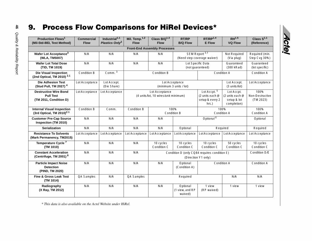
46Q
uality & R
eliability Report
9. Process Flow Comparisons for HiRel Devices*1.4 RH1.5
VQ FlowClass S1.1
(Reference)
er)Not Required
(Via plug)Required (min. Step Cvg 30%)
Guaranteed(300 kRad)
Guaranteed(lot specific)
Condition A Condition A
Lot Accept.(3 units/lot)
Lot Acceptance
t. 5
ch @ ery 2
Lot Accpt.(2 units each @
setup & lot completion)
100% Non-Destructive
(TM 2023)
100%Condition A
100%Condition A
l 6 Optional
Required Required
ance Lot Acceptance Lot Acceptance
es n C
50 cycles Condition C
10 cycles Condition C
ondition E) Condition D/E
Condition A Condition A
N/A N/A
ed)1 view 1 view
Production Flows1
(Mil-Std-883, Test Method)Commercial
FlowIndustrial1.1
Plastics Only2Mil. Temp.1.2
FlowClass B/Q1.3
FlowRT/RP
B/Q FlowRT/RPE Flow
Front-End Assembly Processes
Wafer Lot Acceptance3
(WLA, TM5007)N/A N/A N/A N/A SEM Report 3.1
(Need step coverage waiv
Wafer Lot Total Dose (TID, TM 1019)
N/A N/A N/A N/A Lot Specific Data(not guaranteed)
Die Visual Inspection(2nd Optical, TM 2010) 2.1
Condition B Comm. 3 Condition B
Die Adhesion Test(Stud Pull, TM 2027) 4
Lot Acceptance Lot Accept.(Die Share)
Lot Acceptance (minimum 3 units / lot)
Destructive Wire BondPull Test
(TM 2011, Condition D)
Lot Acceptance Lot Acceptance Lot Acceptance (4 units/lot, 10 wires/unit minimum)
Lot Accp(2 units easetup & ev
hrs.)
Internal Visual Inspection(3rd Optical, TM 2010)2.1
Condition B Comm. Condition B 100%Condition B
Customer Pre-Cap Source Inspection (TM 2010)
N/A N/A N/A N/A Optiona
Serialization N/A N/A N/A N/A Optional
Resistance To Solvents(Mark Permanency, TM2015)
Lot Acceptance Lot Acceptance Lot Acceptance Lot Acceptance Lot Acceptance Lot Accept
Temperature Cycle 7
(TM 1010)N/A N/A N/A 10 cycles
Condition C10 cycles
Condition C10 cycl
Conditio
Constant Acceleration(Centrifuge, TM 2001) 8
N/A N/A N/A Condition D (only CQ84 requires c
(Direction Y1 only)
Particle Impact Noise Detection
(PIND, TM 2020)
N/A N/A N/A N/A Optional(Condition A)
Fine & Gross Leak Test(TM 1014)
QA Samples N/A QA Samples Required
Radiography(X Ray, TM 2012)
N/A N/A N/A N/A Optional (1 view, and RP
waived)
1 view(RP waiv
* This data is also available on the Actel Website under HiRel.

Quality &
Reliability R
eport47
Required
N/A
Required(T0 test)
Required
s @ 125 oCition D
240 hours @ 125
oC
uired per Actel spec., 5005 Group A s 1, 7, & 9)
Required
Required(T1 test)
Required
uiredtel SMD)
Required
P ≤ 5% overall, and ≤ 3% functional(T1 only)
N/A
Cond. C144 hours at
125oC
Cond. C72 hours at
150 oC
M5005Required
Required(T2 test)
Required
uiredtel SMDs)
Required
P ≤ 5% overall, and ≤ 3% functional (T2 only)
≤ 5% overall, and ≤ 3% functional
RH1.5
VQ FlowClass S1.1
(Reference)
Back-End Electrical Testing/Screening Processes
Electrical Test@ Room Temperature
(Commercial Test)
Required(100% testing per Actel spec., including TM5005 Group A Subgroups 1,7, & 9)
QC Monitor(Programming)
Sample per Wafer Lot (Per Actel Specification)
Pre Burn-InRead & Record (R&R)
N/A N/A N/A N/A N/A Required
Dynamic Burn- In(TM 1015)
N/A N/A N/A 80 hours @ 150oC(Cond. D, Accelerated BI)
240 hourCond
Post Burn-In (Interim)Electrical Test
@ Room Temperature
N/A N/A N/A N/A N/A Req(100% testing
including TMSubgroup
Post Burn-In (Interim)Read & Record (R&R)
N/A N/A N/A N/A N/A Required
Delta Calculation N/A N/A N/A N/A N/A Req(Per Ac
ercent Defective Allowance(PDA, TM 5004)
N/A N/A N/A N/A N/A N/A
Static Burn In(TM 1015)
N/A N/A N/A N/A N/A Cond. C72 hours at
150 oC
Post Burn-InElectrical Test
@ Room Temperature
N/A N/A N/A Required(100% testing per Actel spec., including T
Group A Subgroups 1 & 7)
Post Burn-InRead & Record (R&R)
N/A N/A N/A N/A N/A Required
Delta Calculation N/A N/A N/A N/A N/A Req(Per Ac
ercent Defective Allowance(PDA, TM 5004)
N/A N/A N/A PDA ≤ 5% overall ≤ 5% overall, and ≤ 3% functional
Production Flows1
(Mil-Std-883, Test Method)Commercial
FlowIndustrial1.1
Plastics Only2Mil. Temp.1.2
FlowClass B/Q1.3
FlowRT/RP
B/Q FlowRT/RP1.4
E Flow

48Q
uality & R
eliability Report
Subgroups 3, 8b, & 11)Required
/A Included 9
(T2 test)N/A
Subgroups 2, 8a, & 10)Required
/A Included 9
(T2 test)
N/A
M5005 N/A N/A
Required Required
ired Required Required
data onlyoduct qualification)
Required
0% of Waived per Mil-PRF-38535 Appendix B11.1.1
116 / lot
.1-4 for s S,
& B.6 nal)
Generic data Group B test for Class S
eric Generic Generic
eric Generic Generic
ly11.5.1 RHA11.5.2
QualifiedRequired
Lot Specific
Production Flows1
(Mil-Std-883, Test Method)Commercial
FlowIndustrial1.1
Plastics Only2Mil. Temp.1.2
FlowClass B/Q1.3
FlowRT/RP
B/Q FlowRT/RP1.4
E FlowRH1.5
VQ FlowClass S1.1
(Reference)
Final Electrical Test (@ -55oC) 2.2
N/A N/A Required(100% testing per Actel spec., including TM5005 Group A
Temperature TestRead & Record (R&R)
N/A N/A N/A N/A N/A N
Final Electrical Test(@ +125oC) 2.2
N/A 0.1% AQLSample Test
@ +85oC
Required(100% testing per Actel spec., including TM5005 Group A
Temperature TestRead & Record (R&R)
N/A N/A N/A N/A N/A N
QA Electrical Test@ Room Temperature 2.2
N/A 0.1% AQLSample Test
0.1% AQLSample Test
Required 5.2
(100% testing per Actel spec., including TGroup A Subgroups 1,7, & 9)
Fine & Gross Leak Test 10
(TM 1014)N/A N/A N/A N/A N/A
External Visual Inspection(TM 2009)
Per Actel Specification Only Required Required Requ
Radiation Latch-Up(TM 1020)
N/A N/A N/A N/A Generic (tested on initial pr
Quality/Technology Conformance Inspection (QCI/TCI, TM5005)
Group A 11.1 N/A N/A N/A In-line group A testing is performed on 10devices at all 3 temperatures
Group B 11.2 N/A N/A N/A Group B test for Class B Group BClas
(B.5 optio
Group C 11.3 N/A N/A N/A Generic Generic Gen
Group D 11.4 N/A N/A N/A Generic Generic Gen
Group E 11.5 N/A N/A N/A N/A Lot Specific TID Test On(No Guarantee)

Notes:
1. Production Flows:All screening tests listed in the table are performed on 100% of products except those specified as Lot Acceptance or QA Samples.
1. 1 Both Industrial and Class S flows are for reference only, and are not offered in ceramic packages.
1. 2 Military Temperature flow is offered in both ceramic and plastic packages (see note 11 for mil-temp plastic devices).
1. 3 Class B and Class Q process flows are identical and meet the requirements per Appendix A MIL-PRF-38535.Since Actel has been QML certified by DSCC since February 1998, all new SMD devices are assigned with level Q SMD part number.
1. 4 Extended flows (E flow) meet the requirements per MIL-PRF-38535 Appendix A for class S, with the exceptions shown on the above comparison table between E flow and Class S.
1. 5 RH VQ Flow is the production flow used for Actel RH1020 and RH1280 devices. It meets all the requirements in appendix B of MIL-PRF-38535 except the lot specific TCI. It has the Class V level screening, but without the lot specific TCI tests, therefore, both RH1020 and RH1280 SMD part numbers are assigned as Q level only.
2. Plastic-molded packages are offered in 3 application temperature ranges:
Commercial (0oC to +70oC), Industrial (–40oC to +85oC), and Military (–55oC to +125oC).
2. 1 For all plastic-molded packages, both second and third optical visual inspection are based on AQL 0.65% sampling plan with 100% re-inspection if failed sampling plan. Visual inspection criteria are based on vendors’ internal specifications, which are generally based on, but not necessary in full compliance with MIL-STD-883, TM2010, Condition B, Internal Visual Inspection.
2. 2 Commercial devices are 100% electrical tested at room temperature only.Industrial devices are 100% electrical tested at room temperature, and 0.1% AQL sampling
test at +85oC. No testing at –40 oC, which is guaranteed by design.Military temperature devices are up-screened from commercial devices with 100% burn-in (only when required by customers) and 100% temperature tests.Guarantee for moisture sensitivity on plastic devices are:• Level 3: PLCC, PQFP, TQFP, VQFP, and BGA packages.• Level 4: RQFP with exposed heat sink.CQFP and CPGA are hermetic packages, which are not subjected to moisture sensitivity issues.
3. Wafer Lot Acceptance (WLA)
3. 1 SEM inspection (TM2018) is waived for devices with via plugs, which include:RH (1.0/0.8µ) devices, XL and DX (0.6µ) devices, MX (0.45µ) devices, A54SX (0.35µ) devices. Other than the above devices, waivers are required for reduced step coverage that don’t meet the 30% minimum requirement per TM2018 section 3.7.2. These devices are:ACT 1 and ACT 2 (1.0µ) devices, ACT3 (0.8µ) devices, and RT54SX (0.6 µ) devices.• ACT 1, ACT 2, ACT 3 device families, typical minimum step coverages are >14% (including barrier metal).• RT54SX device family, typical reduced step coverages are between 4% to 10%, but much more when barrier metal is included.
Quality & Reliability Report 49

4. Only a minimum of 2 units is used for die attach stud pull and destructive wire pull per each assembly lot prior to 9/30/99.
5. E-flow RT devices produced at Kyocera SCA will perform 100% destructive wire pull on setup units. However, E-flow RP devices produced at Space Electronics Inc. (SEi) will perform only 30% destructive wire pull on setup units due to the very low through-put of their semi-automatic wire bonding machines.
6. Precap CSI requires special assembly build to allow scheduling for customer precap CSI dates. Minimum order quantity will be required to start a custom assembly lot. Actel may refuse customer precap CSI due to an already high inventory position. The customer can always purchase extra units and perform DPA as a substitute for the precap CSI requirement.
7. For the Temperature Cycling Test, all devices except RH devices perform 10 cycles only. This still meets the QML requirement.
8. Constant acceleration tested on devices with CQ84 packages are condition D only for each assembly lot prior to 9/30/99.
9. For RH devices, Read and Record is not required at –55oC and +125oC per mil-spec. They are performed as a preference of LMSEC (Lockheed Martin Space Electronics and Communications, Actel vendor for RH device production).
10. The second Fine & Gross Leak Test is to be completed as the final screening step after the completion of all electrical tests.
11. Quality/Technology Conformance Inspection (QCI/TCI): All QCI/TCI (Group A, B, C, D, & E) tests are performed per MIL-STD-883 Method 5005 or MIL-PRF-38535.
11. 1 Group A electrical tests are lot specific with a sample size of 116/lot or 100% if fewer than 116 units.
11. 1.1 Actel TRB approved the removal of the end-of-line group A electrical tests at all 3 temperatures starting 12/15/99.Actel has already implemented in-line group A tests at final electrical tests for all 3 temperatures, which are done on 100% of the devices at tighter limits, therefore, eliminating the redundant end-of-line group A testing will improve process efficiency without affecting the device quality and reliability. The Actel in-line group A testing complies with MIL-PRF-38535, Appendix J, section J.3.11 Inline TCI Testing (option 2).
11. 1.2 Group A can be waived for QML line per MIL-PRF-38535 Appendix B, which is done at LMFS for RH device production.
11. 1.3 Starting 12/15/99, QA electrical testing on 100% of devices is also implemented after the group A electrical testing are eliminated to ensure devices are not damaged due to test setup at hot and cold tests.
11. 2 Group B for Class E and Class V includes 1000 hrs life test and thermal/mechanical test. Group B for class B devices are performed for class B devices. Group B for class S devices are performed for E-flow, however, only B.1 to B.4 are performed on each assembly lot. B.5 1000 hrs life test and B.6 thermal/mechanical test are only performed when customer requests the test and pays for the cost. Assembly in-line process monitoring data can be used as part of the group B data.
11. 3 Group C is performed once every 4 quarters for each wafer fab technology plus one quarter of extension time.
50 Quality & Reliability Report

11. 4 Group D is performed once every 6 months for each assembly foundry plus 10 weeks of extension time. RP devices are produced only when needed at very low run rates, so group D is performed only when customer requests the test and pays for the cost.
11. 5 Group E RHA TCI tests:
11. 5.1 Group E test data for RT/RP devices are performed on test samples only. All RT/RP devices have TID (TM1019) data done on all wafer lots.
11. 5.2 Group E for RH devices are performed on the RHA qualification lots only.
12. Die business for all die are 100% inspected per MIL-STD-883, Method 2010, Condition B.
Quality & Reliability Report 51
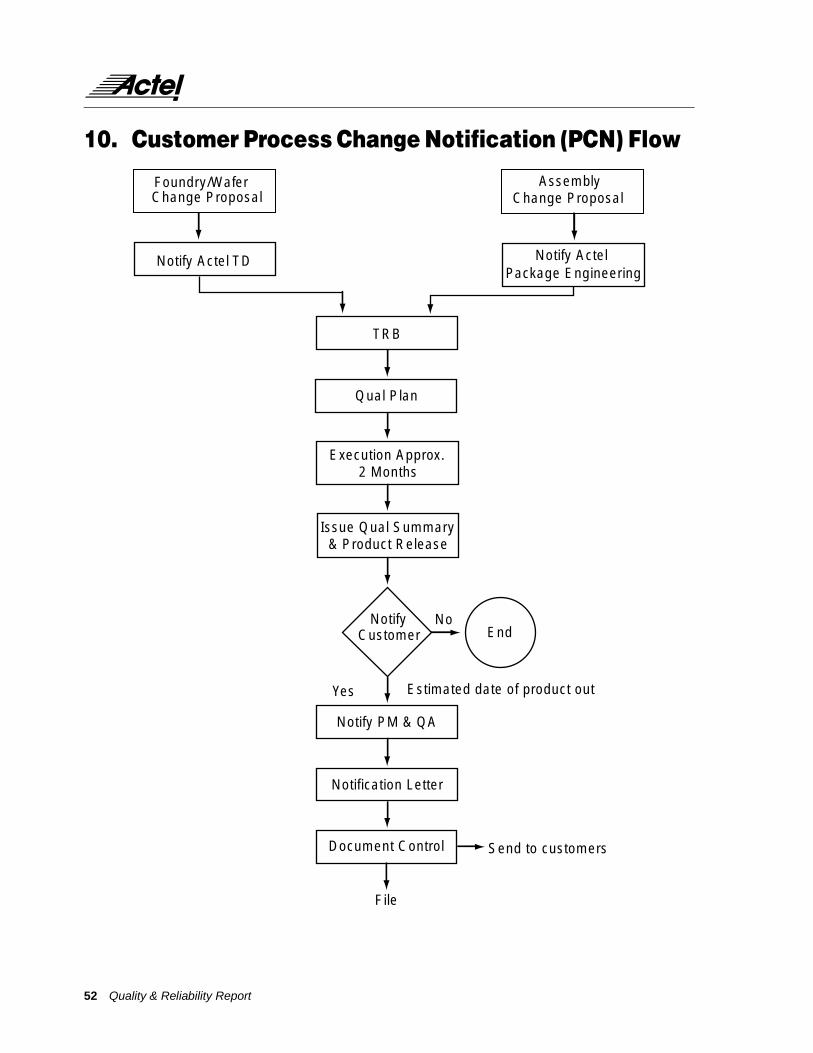
10. Customer Process Change Notification (PCN) Flow
Foundry/WaferChange Proposal
Notify Actel TD
TRB
Execution Approx.2 Months
Issue Qual Summary& Product Release
No
Assembly Change Proposal
Notify Actel Package Engineering
Qual Plan
Notify PM & QA
Notification Letter
Document Control
NotifyCustomer
Yes Estimated date of product out
End
Send to customers
File
52 Quality & Reliability Report
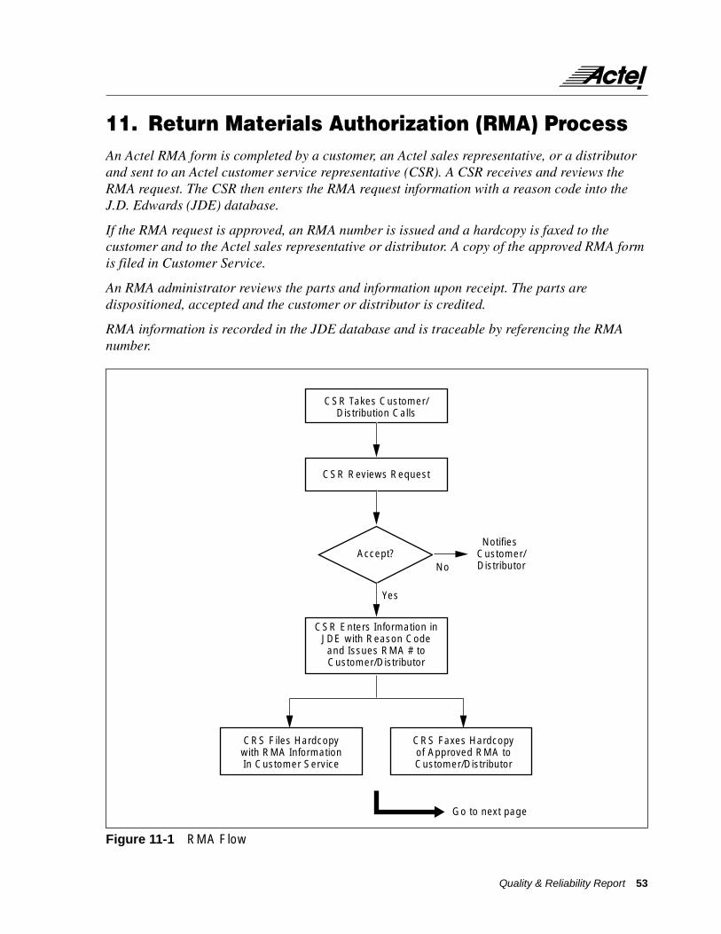
11. Return Materials Authorization (RMA) Process An Actel RMA form is completed by a customer, an Actel sales representative, or a distributor and sent to an Actel customer service representative (CSR). A CSR receives and reviews the RMA request. The CSR then enters the RMA request information with a reason code into the J.D. Edwards (JDE) database.
If the RMA request is approved, an RMA number is issued and a hardcopy is faxed to the customer and to the Actel sales representative or distributor. A copy of the approved RMA form is filed in Customer Service.
An RMA administrator reviews the parts and information upon receipt. The parts are dispositioned, accepted and the customer or distributor is credited.
RMA information is recorded in the JDE database and is traceable by referencing the RMA number.
Figure 11-1 RMA Flow
CSR Takes Customer/Distribution Calls
CSR Reviews Request
Accept?No
Notifies Customer/Distributor
Yes
CSR Enters Information inJDE with Reason Codeand Issues RMA # toCustomer/Distributor
CRS Files Hardcopywith RMA InformationIn Customer Service
CRS Faxes Hardcopyof Approved RMA toCustomer/Distributor
Go to next page
Quality & Reliability Report 53

Figure 11-1 RMA Flow (Continued)
RMA AdministratorReceives Parts fromCustomer/Distributor
Verify Part Numberand Count
RMA is Dispositioned.JDE is Updated withDisposition Code
Accept?Return To Customer/Distributor
Credit Customer/Distributor or Replace Parts
No
Yes
54 Quality & Reliability Report

12. Failure Analysis (FA) ProcessAn application engineering (AE) or a CSR receives a FA request from a customer, an Actel sales representative, or a distributor. The AE evaluates the case. If the FA request is accepted, the AE issues a case number for tracking and records failure descriptions.
An FA/RMA administrator receives the parts and forwards them to Product Engineering for failure analysis. The failures are analyzed, cause is determined and, if necessary, corrective action is initiated. Upon completion, a failure analysis report is distributed to AE, QA, CSR, and the sales representative or distributor. A copy of the report is forwarded to Document Control for filing.
Quality & Reliability Report 55
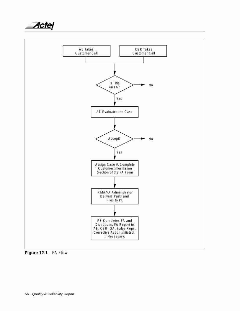
Figure 12-1 FA Flow
AE Evaluates the Case
Accept?
Is Thisan FA? No
Yes
PE Completes FA andDistrubutes FA Report to
AE, CSR, QA, Sales Reps.Corrective Action Initiated,
If Necessary.
AE TakesCustomer Call
CSR TakesCustomer Call
Assign Case #. CompleteCustomer Information
Section of the FA Form
RMA/FA AdministratorDelivers Parts and
Files to PE
No
Yes
56 Quality & Reliability Report

A. Actel and the Antifuse—A Technical Backgrounder
IntroductionThrough the years, the design of digital logic circuits has evolved from working with small-scale integrated circuits (ICs) containing discrete gates to use of large-scale and very-large-scale ICs (VLS1) containing many thousands of gates. A number of commonly-used functions became available in the form of high-density circuits. Yet designers still retained the need to use small-scale ICs, even discrete gates, to solve interface problems and to implement their unique designs. The advent of the field-programmable gate array (FPGA) encapsulated the design flexibility provided by small-scale lCs into a high-density circuit.
The applications for FPGAs are legion. Wherever a design uses a substantial amount of small- and medium-scale ICs there exists the potential for an FPGA to provide a faster, more compact, more reliable solution. FPGAs also excel in new designs, where VLSI alternatives do not exist and the cost of custom ICs is prohibitive. Where complex designs must undergo minor updates to match changing market demands, where designs must be initiated without final specifications in hand, or where production volumes are too low to amortize a custom circuit’s setup costs, FPGAs have a home.
The market for FPGAs is substantial and growing. In 1993 the total market for FPGAs and other high capacity programmable logic devices (HCPLDs) exceeded $539M. Dataquest forecasts put the market at $2124M in 1998, representing a compound annual growth rate of 32%. Indeed, the market has attracted a number of vendors, each touting its architecture and technology as the best solution to the needs of logic designers.
Actel Corporation entered the programmable logic market in 1988 with the shipment of its first FPGA. The company’s products now include the ACT 1, ACT 2, 1200XL, and ACT 3 logic families that span 1,200 to 10,000 gates in density. All are based on the company’s multi-patented channeled array architecture and the PLICE (programmable low-impedance circuit element) antifuse.
An antifuse, as its name implies, is like a fuse in reverse. The antifuse begins as a high-impedance (essentially open) circuit element and changes to a low-impedance connection when subjected to a programming voltage. The change is irreversible and highly reliable.
Actel’s channeled array architecture uses the PLICE antifuse to great advantage. The array comprises horizontal rows of logic blocks alternating with channels of pre-defined interconnect tracks segmented into varying lengths. The input and output ports of each logic block connect to vertical tracks that span several logic rows and interconnect channels. The vertical and horizontal tracks are insulated from one another but at each crossover lies an antifuse. When programmed, the antifuse connects the two tracks together. Selectively programming the antifuses will create a circuit path between one logic block and another. (See Figure A-1.)
Quality & Reliability Report 57

The network of horizontal and vertical interconnect tracts in the ACT family allows arbitrary and flexible interconnections among logic blocks. All speed-critical interconnections can be accomplished programming only two antifuses. Most other connections in the design use two or three antifuses, but never more than four. The result is a device that lets designers utilize in excess of 80%, and in many applications, 100% of the available logic blocks before all available routing channels are taken. And that routing is flexible enough that CAE tools can achieve 100% automatic placement and routing. These levels of utilization and routability are comparable to conventional gate arrays of similar size.
The PLICE antifuse is an integral part of this architecture and helps it to be fully scaleable. The antifuses reside entirely within the interconnect channels and are smaller than the space from one track to the next. Thus, the antifuses interconnects occupy no additional die area. Further, they are small enough that improvements in process technology that shrink line spacing won’t crowd the antifuses.
The synergy created by the combination of architecture and antifuse technology has allowed Actel to extend its methodology over four generations of parts. The product line now includes a breadth of parts that satisfy a variety of designer’s requirements. For example, the ACT 3 family offers the highest performance and highest pin-to-gate ratio available in high capacity programmable logic today. The A1440A 4000-gate device can provide serial communications and pipelined datapath designs with clock speeds up to 250 MHz. Devices such as the A1240XL 4000-gate FPGA can achieve up to 60 MHz overall system operation with 16-bit pre-scale counters that operate at 130 MHz. And for high-volume applications, the ACT 1 family provides the lowest cost production FPGAs available.
As a result, Actel is among the fastest-growing FPGA companies. Actel has risen to rank among the top 5 suppliers of CMOS programmable logic.
Figure A-1
Modules
UnprogrammedAntifuse
Modules
Vertical Track
Horizontal Control
Horizontal Track
ProgrammedAntifuse
58 Quality & Reliability Report

Antifuse vs. Memory-Based Programmable LogicWhen it was founded in 1985, Actel sought the best long-term solution to the needs of high-performance programmable logic. It considered a variety of alternatives, examining various antifuse structures. Actel chose to pair an antifuse interconnect scheme with a gate-array-like architecture in order to achieve the highest possible circuit density and, consequently, lowest cost on a per-gate basis.
Two kinds of gate array structures exist: channeled arrays and channeless sea-of-gates arrays. The channeled array divides the silicon into strips of logic blocks interspersed with channels containing metal tracks. The sea-of-gates structure uses a myriad of small logic blocks (gates) that cover the silicon. In both cases a network of metal traces provides potential pathways for carrying signals to and from the logic blocks. In the channeled array, the traces within the channels can carry signals alongside the logic. A second layer of metal traces, insulated from the channels and logic blocks, can carry signals across the logic. The sea-of-gates array uses three insulated metal trace layers, two of which run at right angles and the third layer is used to connect the logic blocks. In either case a route from one logic element to another lies along a combination of traces within the two layers, but the traces aren’t connected, yet.
A programmable gate array offers the user a means of selectively connecting trace segments in the two layers to form complete circuits between logic elements. The methods used to provide that connection include both memory-driven transistor switches and physical-change structures. With memory-driven interconnections, an EPROM or RAM cell provides a signal that controls a pass transistor. When turned on, the transistor provides a signal path between the trace segments it bridges. When off, it isolates the two. By programming the memory cells, the user establishes logic circuits.
Physical-change structures, on the other hand, use an interconnection element that will be physically altered during the programming process. The alteration is permanent, eliminating the need for a memory circuit. Two types of such interconnection elements are possible: the fuse and the antifuse.
The fuse is a familiar structure: a conducting metal filament that is destroyed when subjected to excessive heat or current, creating an open circuit. Fuses have been used for years as programming elements for memories and simple programmable logic. They are ill-suited to FPGAs, however, because of the many potential connections.
A fuse-based programmable gate array (PGA) would need to start out with all possible connections among the logic elements already made. The user then would remove all the unwanted connections in order to leave the pattern desired. Because a programmed gate array typically uses only 2% of its possible connections, this is rather like building a box by hollowing out a large block of wood—highly inefficient. Fuse-based PGAs can be implemented for factory programming, however, using a laser to cut the unwanted fuses.
Quality & Reliability Report 59

In contrast to the fuse, the antifuse is a non-conducting circuit element that becomes conducting following application of a programming voltage and current across its terminals. Configuring an antifuse-based FPGA, therefore, requires programming only those connections that are desired, leaving the others alone. You only build the walls you need for your box.
Of all these structures, the antifuse represents the most efficient use of die area. The memory cells needed for memory-based interconnect occupy considerable silicon area. An SRAM cell, for example, needs at least 3 transistors in addition to the pass transistor for the connection. Further, the pass transistors have to be relatively large to get high performance. This multitude of large transistors occupies more space than the traces alone need. The result is either a relatively large die or limits to the number of interconnections per chip.
An antifuse structure is much more compact. Antifuses typically consist of a thin insulating layer between contact points that begins conducting under application of high voltage, typically 12–20V. Once the insulation starts conducting, the antifuse’s terminals melt together and form a permanent conducting channel through the insulation. That channel is typically a tenth the size of the tracks being connected. Thus, the antifuse can occupy the space between metal traces, taking up no additional die area. This allows the antifuse to be placed at every potential connection point without affecting the die size.
The antifuse FPGA does lose some chip area because it needs on-chip high-voltage programming circuits. These circuits reside on the chip’s edges, however, rather than at each interconnect junction. Thus the die area occupied by the high-voltage drive transistors does not restrict the interconnect density achievable in the rest of the chip, unlike the transistors in a memory-based FPGA. Further, as semiconductor processes scale to smaller feature sizes and allow higher gate capacity devices, the relative area occupied by the high-voltage circuits decreases.
In addition to the die area advantages, the antifuse provides a connection with lower resistance and capacitance than the pass transistors. Lower resistance and capacitance translates into smaller propagation delays, resulting in faster overall circuits.
Antifuse TechnologyThe antifuse concept dates back to at least 1951, when it was considered for use in memories. The basic antifuse is a thin insulating layer between conductors that gets altered (programmed) by the application of high voltage. The alteration is non-volatile, i.e., it remains after removal of the voltage. Once the change has occurred, a low-resistance path exists between the conductors. The nature of that path is determined by the type of antifuse structure used. At present, two types of antifuse are commercially produced: the amorphous silicon antifuse and dielectric antifuse.
The amorphous silicon antifuse uses a non-crystalline form of silicon between the conductors, which are typically metal. Under high voltage a section of that amorphous silicon undergoes a phase change and atoms from the metal layers it separates migrate into the silicon material. The
60 Quality & Reliability Report

result is a thin conducting filament composed of a complex mixture of silicon and metal. (For details, see “Appendix A—The Structure of Antifuses” on page 66.) The size and resistance of the filament is dependent on the amount of programming current that flowed during its creation.
This structure has been investigated for years and has presented a number of technical hurdles. To keep within reason the programming voltage needed, the amorphous layer must be thin. Early attempts to create these thin layers either required processes too costly for high-volume production or resulted in significant thickness variation because of process equipment limitations. The consequence was a history of devices with unpredictable performance. Only in the last 3–4 years has process technology been sufficiently accurate to control the amorphous silicon thickness.
A more persistent problem with some amorphous silicon antifuses has been their response to high-current pulses. The programmed antifuses sometimes revert to a high-impedance state due to cracking or a phenomenon called read disturb. The result is that the antifuse’s resistance jumps, which will change the corresponding logic circuit’s propagation delays and may even look to.the logic like an open-circuit. This reversion tends to be self-healing; normal logic-high voltages are sufficient to reprogram the disturbed antifuse. However, there is no guarantee that the node containing the disturbed antifuse will see a logic-high voltage again, once the change has occurred. Thus, the tendency to self-heal is not a reliable antidote. Instead, the FPGA design must limit the current flow through the antifuse to avoid stressing the filament.
The other antifuse type, the dielectric antifuse, uses oxide (glass) as the insulating layer. Application of high voltage creates multiple conducting filaments which are prone to self-healing. (See Figure A-2.)
Actel solved that problem with its patented PLICE antifuse structure. Instead of using a single oxide layer, the PLICE antifuse uses a sandwich of oxide, nitride, and oxide (ONO). The ONO layer lies between a polysilicon conductor and a heavily-doped n+ diffusion region of the base silicon wafer. Under the programming voltage, the ONO sandwich melts and the base wafer grows an epitaxial “bump” into the polysilicon in the shape of a dome. Growth of the bump shatters the ONO layer, allowing diffusion of the substrate n+ into the polysilicon to form a low-resistance path.
Figure A-2
Oxide Oxide
Polysilicon
ONO Layer
Quality & Reliability Report 61
The bump typically is 10x taller than the ONO layer thickness, preventing any possibility of reinstating the oxide barrier. The bump’s size also makes the structure tolerant of current-induced stresses. Thus, the PLICE antifuse can safely handle much higher currents than can amorphous silicon. If anything, the high currents would increase the bump’s size, strengthening the connection.
Although the PLICE antifuse uses the base silicon as part of its connection between metal layers, it does not steal any die area from the logic circuits in a channeled gate array. The PLICE structure is small enough to fit in the space between metal traces in the channel.
Evolution Antifuse Alternatives Low resistance and capacitance values are among the primary attributes of a good programmable connection for logic. The need for low resistance comes from its interaction with both the connection’s capacitance and the parasitic capacitance that occurs in the metal interconnection network and the input structures of logic gates.
The greater the capacitance in a circuit, the more drive current the circuit requires in order to quickly shift logic states. However, the connection’s resistance attenuates the drive signal, restricting the amount of current available to change logic states. The combined effect of this resistance and capacitance is to slow the propagation of electrical signals through the circuit. This slowing, in turn, limits the clock frequency the logic can use. Keeping the connection’s capacitance and programmed resistance low minimizes the problem.
Comparing antifuse alternatives solely on the basis of capacitance and typical programmed resistance, however, is to take a near-sighted view. There may be other factors limiting the circuit’s clock speed. One such factor is extendability, how well the antifuse structure works over a range of IC sizes. Another is scaleability, how readily the structure shrinks as process lithography improves. The key to creating a useful product is finding an optimum combination of all factors.
Consider, for example, the current-carrying capacity of an antifuse structure. Amorphous antifuses, as already described, risk being damaged by too great a current. Thus, an FPGA using amorphous antifuses must be designed to avoid current spikes. Yet current spikes are common in digital circuits. Circuit capacitance and logic switching speed determine the size of those spikes. Therefore, the amorphous-antifuse FPGA must place limits on clock edge rate based on the circuit’s capacitance.
One prominent contributor to circuit capacitance is the metal interconnect track. Its capacitance is a function of its length; the longer the track, the greater the capacitance. As the array size gets larger, then, the amorphous-antifuse FPGA must either reduce circuit speed or limit track length to keep current spikes under control. Reducing circuit speed is an obvious disadvantage. Limiting track length is also a disadvantage, however, because it reduces the user’s ability to fully utilize the available gates. Gates widely separated cannot be used in the same circuit.
62 Quality & Reliability Report
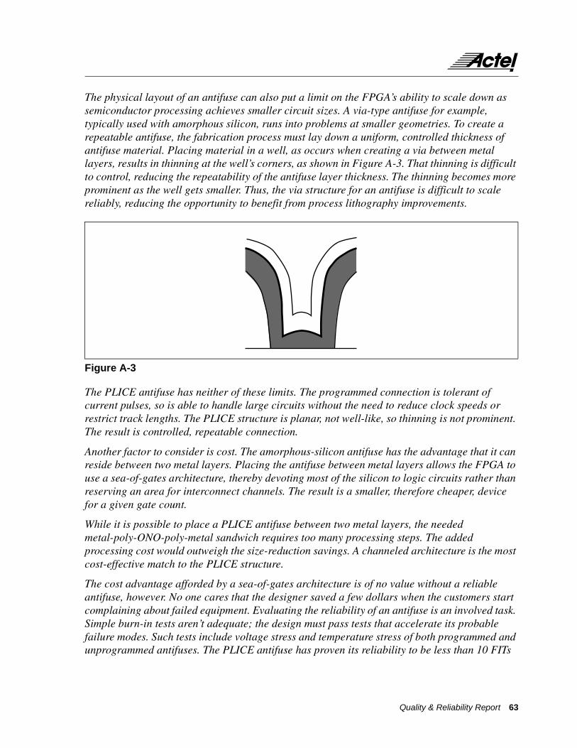
The physical layout of an antifuse can also put a limit on the FPGA’s ability to scale down as semiconductor processing achieves smaller circuit sizes. A via-type antifuse for example, typically used with amorphous silicon, runs into problems at smaller geometries. To create a repeatable antifuse, the fabrication process must lay down a uniform, controlled thickness of antifuse material. Placing material in a well, as occurs when creating a via between metal layers, results in thinning at the well’s corners, as shown in Figure A-3. That thinning is difficult to control, reducing the repeatability of the antifuse layer thickness. The thinning becomes more prominent as the well gets smaller. Thus, the via structure for an antifuse is difficult to scale reliably, reducing the opportunity to benefit from process lithography improvements.
The PLICE antifuse has neither of these limits. The programmed connection is tolerant of current pulses, so is able to handle large circuits without the need to reduce clock speeds or restrict track lengths. The PLICE structure is planar, not well-like, so thinning is not prominent. The result is controlled, repeatable connection.
Another factor to consider is cost. The amorphous-silicon antifuse has the advantage that it can reside between two metal layers. Placing the antifuse between metal layers allows the FPGA to use a sea-of-gates architecture, thereby devoting most of the silicon to logic circuits rather than reserving an area for interconnect channels. The result is a smaller, therefore cheaper, device for a given gate count.
While it is possible to place a PLICE antifuse between two metal layers, the needed metal-poly-ONO-poly-metal sandwich requires too many processing steps. The added processing cost would outweigh the size-reduction savings. A channeled architecture is the most cost-effective match to the PLICE structure.
The cost advantage afforded by a sea-of-gates architecture is of no value without a reliable antifuse, however. No one cares that the designer saved a few dollars when the customers start complaining about failed equipment. Evaluating the reliability of an antifuse is an involved task. Simple burn-in tests aren’t adequate; the design must pass tests that accelerate its probable failure modes. Such tests include voltage stress and temperature stress of both programmed and unprogrammed antifuses. The PLICE antifuse has proven its reliability to be less than 10 FITs
Figure A-3
Quality & Reliability Report 63

(failures in time; 0.0001%/1000 hours) over 8 million device hours (125°C) of testing. That’s equivalent to a device lifetime greater than 40 years. Other antifuse structures have yet to prove similar reliability levels.
Numerous additional factors need consideration when evaluating antifuse structures. Table A-1 summarizes several factors and their significance.
User Benefits of Actel’s Technology Actel has conducted ongoing research into antifuse technology since its founding. In addition to developing its PLICE antifuse, the company has investigated a variety of other structures, including metal-to-metal PLICE, metal-to-metal amorphous silicon, and single-oxide dielectric. It has also developed and patented both channeled array and sea-of-gates FPGA architectures. It has picked and chosen from those alternatives based on four user benefits: cost, performance, extendability, and reliability.
The PLICE antifuse coupled with the channeled array architecture represents the most cost-effective design available. The antifuse structure allows a smaller die than equivalent memory-based FPGAs and does not need external memory devices to maintain its programming during power loss. The antifuse’s small size also allows the chip to provide extensive routing resources, yielding 85% to 95% utilization of the array’s logic blocks. This utilization efficiency allows designers to put more circuits into the smaller devices.
The extensive routing resources also reduce the risk of making logic changes. Once an initial design is complete, FPGA pinout patterns get cast in copper by the printed-circuit board design. An FPGA with limited resources, however, may not be automatically routable to the same l/O pin pattern following a logic change. Designers must then either change the circuit board design (a step FPGAs were supposed to help avoid) or spend time hand-routing the FPGA. The ACT family’s abundance of routing resources avoids such problems.
Compared to SRAM and EPROM memory-based devices, the PLICE antifuse offers lower resistance and capacitance, thus, greater circuit speeds. The PLICE also provides a programmed resistance within a narrow range, making circuit operation predictable and repeatable. The predictability makes for more accurate simulations, allowing users to catch timing bugs early on. The repeatability lets designers to use tighter timing tolerances and wring maximum performance out of the FPGA.
Table A-1
Factor Significance
Leakage Current Because there are many antifuses on a chip, leakage currents can amount to a consid-erable power consumption. A 10 nano-Ampere leakage current in each of the typical 750,000 antifuses on a large FPGA would waste 7.5 mA.
Programming Voltage and Current
The higher the voltage and current needed, the larger the drive transistor must be and the greater the chip area occupied by programming circuits.
Range of Programmed Resistance
A predictable, narrow range for the resistance values of programmed antifuses allows accurate timing estimates during simulation and repeatable performance in production.
64 Quality & Reliability Report

While the amorphous-silicon metal-to-metal antifuse and sea-of-gates architecture looks promising, Actel’s research has shown that the programmed link is fragile under over-current conditions. Such conditions occur frequently in normal operation, making the field reliability of amorphous antifuses questionable. High circuit speeds and large array sizes increase the likelihood of over-current failure, limiting the speed and size attainable with an amorphous antifuse.
The PLICE antifuse has proven its reliability over many millions of device hours. Once programmed, the structure is highly resistant to damage from current spikes. It does not undergo any form of self-healing, so its programmed resistance remains stable over its expected 40-year+ lifetime. The result is an FPGA that provides predictable, repeatable, consistent performance over a system’s product life.
Future Directions in Antifuse Technology The evidence indicates that the PLICE antifuse, coupled with Actel’s patented channeled-array architecture, represents the best combination of cost, performance, and reliability among today’s FPGA architectures. Building on that foundation, the company has extended its designs to a 0.6-micron process and brought that process on line at three foundries. The PLICE structure benefits from this by scaling in both size and effective speed. Actel plans to soon introduce additional device families based on ONO and the channeled array architecture.
Actel continues to investigate all alternatives, however, to keep providing designers with the best FPGAs possible. The sea-of-gates architecture with a metal-to-metal antifuse has great potential, yet Actel’s extensive antifuse research casts doubts on the reliability of existing amorphous silicon antifuses. The company’s answer has been to develop a new generation of metal-to-metal antifuse.
Actel’s development of a sea-of-gates device began as early as 1990. By 1991 it had patented a sea-of-gates architecture. But Actel’s quest for a reliable metal-to-metal antifuse, involving many teams developing alternative approaches in parallel, lead the company to abandon traditional simple via amorphous silicon by 1992.
That quest has been fruitful, however. The company has developed a metal-to-metal (M2M) antifuse that solves the problems encountered with amorphous silicon. Built from a proprietary combination of materials, Actel’s M2M uses a planar structure rather than a via, so corner thinning, and the resulting manufacturability and reliability concerns, does not become a problem at smaller scales. It achieves a leakage current about one-third that of amorphous silicon, a capacitance 25% less, and a cell size 25% smaller.
That, coupled with M2M’s smaller cell size, promises to allow higher densities at lower cost in Actel’s FPGAs. Further, the M2M antifuse’s reliability in the face of current surges will allow the development of large, fast arrays where amorphous silicon must slow down to protect against damaging noise spikes
Quality & Reliability Report 65

Nor is Actel standing still. The company vigorously pursues research into antifuse technology and FPGA architectures. It is committed to continual product improvement in both capability and reliability.
Appendix A—The Structure of Antifuses An antifuse possesses a deceptively simple basic structure. It is a thin layer of insulating material sandwiched between two conductors, forming an open circuit. With the application of a programming-voltage pulse, the insulator melts and forms a conducting path instead. The path remains intact when the voltage pulse ends; a new connection exists.
Although the concept is simple, creating an effective antifuse structure in an integrated circuit is a complex task. Actel was the first company to bring an antifuse-based device to market. Few others have been able to follow.
Actel’s antifuse, called PLICE (programmable low-impedance circuit element), uses polysilicon as one of its conductors, and a diffused n+ region as the second conductor. Each conductor connects to one of the metal layers (M1, M2) that route signals through the FPGA. A sandwich of oxide, nitride, end oxide (ONO), 120A thick, separates the two conductors (See Figure A-4).
In its unprogrammed state, the ONO layer provides a resistance of >100 mega ohms.
Application of a 16V pulse causes the dielectric layers to melt, allowing current to begin flowing across the ONO layer. The current flow stimulates epitaxial crystal growth from the n+ layer into the polysilicon, shattering the ONO layer. Excess dopant from the n+ layer migrates into this crystal. When the programming pulse ends, the antifuse cools. leaving a hemispherical
Figure A-4
M2
M1
M1
Poly
ONO Layer
66 Quality & Reliability Report

crystalline dome between the two conductors (See Figure A-5). A programming current of 5 mA is sufficient to produce a connection with a nominal 600¾ resistance. A programming current of 15 mA creates a 100¾ connection.
Because it uses a diffused n+ region as one of its conductors, the PLICE antifuse needs to be fabricated on top of a silicon layer. The most economical place to locate the PLICE antifuse, then, is on the same base layer as the active circuit elements. It is possible to fabricate a PLICE-style antifuse between metal layers using polysilicon between the metal layers and the antifuse. The added process mask steps, however, make this structure economically unattractive.
Figure A-5
Oxide Oxide
Polysilicon
ONO Layer
Oxide Oxide
Polysilicon
ONO Layer
Before Programming
After Programming
Quality & Reliability Report 67

An antifuse structure that does comfortably fit between metal layers is the amorphous antifuse. This antifuse structure uses non-crystalline (amorphous) silicon as the insulating layer. Between the metal and the amorphous silicon lies a layer of barrier metal. The barrier metal prevents the metal layers from migrating into the silicon under normal operating voltages (See Figure A-6).
Application of a 15V programming pulse causes a phase change within the amorphous silicon. A filament of crystalline silicon forms between the metal layers. That filament is a mixture of silicon, the metal-layer material, and the barrier-metal material. Its precise electrical and mechanical characteristics depend on the materials involved and the amount of current that flowed during the filament’s formation. A current of 25 mA is generally needed h form a low-resistance connection, typically 80–1OO¾.
Once formed, the filament is subject to stresses as current passes through it. Depending on the material mix used, that stress can cause the filament to crack or to electromigrate if the current too great. The result is a jump in resistance of the programmed antifuse. This tendency for resistance shifts puts limits on what the amorphous silicon antifuse can reliably achieve as a circuit element in an FPGA.
Appendix B—The Hidden Cost of ReprogrammabilityOn the surface, reprogrammability may appear to be a no-lose feature in design. The same device can be used time and again rather than using up a new device every time a specification change occurs or a design error is found. Unless reprogrammability is required as part of the system-level design, however, the feature’s hidden costs can substantially outweigh its apparent benefits.
Designers that utilize reprogrammable devices have developed a trial-and-error design philosophy. They try out their design, then examine its output signals to figure out what’s happening. Based solely on these signals, they make an educated guess at what went wrong, and try again. Each attempt requires that they enter design changes, compile the design into a
Figure A-6
Metal 2
Barrier Metal
Metal 1
Amprphous Silicon
68 Quality & Reliability Report

program map, program the device, and check it out. For complex designs this cycle repeats many times. The trial-and-error approach becomes even more difficult and time-consuming if the design uses asynchronous logic. Even seemingly minor changes to an asynchronous design can cause sections that were working to now fail.
Use of a reprogrammable device eliminates the material cost of the trial-and-error approach. The time spent debugging, modifying, and repeating the cycle represents a hidden cost, however, in man-hours and schedule delays. Engineering budgets typically run about $3000/week; successful companies such as 3Com and Hewlett-Packard have estimated that a week’s schedule delay cuts $30,000 from a product’s lifetime profits. Yet, because it eliminates the apparent cost, reprogrammability encourages the trial-and-error approach and corresponding wasted time.
A similar situation existed during the early days of microprocessor-based designs. Because the programmable processor replaced fixed-logic circuits, it eliminated the apparent cost of correcting design flaws on PC boards. Users now know how expensive fixing software by trial-and-error can become. As a result, a host of tools like in-circuit emulators exist to take the guesswork out of correcting errors.
The equivalent for programmable logic design is the simulator. By using a simulator, designers have access to what’s happening inside the design. By providing full modeling of the design, including postroute timing, simulation enables the designer to adopt a debug methodology that is quicker, more controllable, and less frustrating than the trial-and-error approach. Being able to see exactly what is wrong reduces the number of fix-and-retest cycles required to achieve a working design. Surveys indicate that fewer than five cycles are needed to debug a design when designers use simulation.
Some bugs, of course, don’t show up until actual circuit testing of FPGAs with external elements may have been less complete. To prevent trial and error debugging at this stage, Actel provides built-in test circuitry in its FPGAs. The Actionprobe diagnostic circuits allow the user to route internal signals to the output pins of the FPGA for examination. This probing capability provides 100% observability of internal nodes in response to system stimuli and thereby reduces design iterations.
Simulation and test circuits help eliminate guesswork, but they require designers to learn new tools. That’s time and money spent that is not obviously contributing to the project’s completion and many designer won’t bother when they don’t have the specter of expended one-time programmable (OTP) parts to frighten them into it. The weeks saved by encouraging better debug techniques more than justify the 5 or so devices that get consumed.
There are other hidden costs associated with using reprogrammable parts. RAM-based FPGAs, for instance, need an external non-volatile memory to retain configuration data when power is absent. That device has a price, and the board area it occupies has a cost. Further, the design becomes more complex because it needs to suspend operation following power up to allow time for the FPGA to get reconfigured.
Quality & Reliability Report 69

Reprogrammable FPGAs also tend to be more expensive than antifuse FPGAs for a given gate count. The internal memory structures that give an FPGA reprogrammability occupy a significant portion of the device’s area. That extra area makes the reprogrammable part much larger than a Actel’s antifuse-based OTP FPGA, adding die cost.
The extra area occupied by those memory structures also compels memory-based FPGA manufacturers to restrict routing resources to reduce the associated memory penalty. With restricted routing, a design may not efficiently utilize the FPGA’s available logic. That, in turn, may force designers to use a size FPGA larger than expected, further increasing cost.
Restricted routing can also add to the cost of design changes. Once a design has been committed to a PCB, users don’t want internal logic changes to alter the FPGA’s pinout. Yet a device with sparse interconnect resources may not be routable to a set pinout following a logic change. Worse, the new logic design may be routable, but suffer performance problems because of changes to internal circuit delays.
The antifuse-based Actel parts offer abundant routing with little area penalty because the antifuse structures fit into the otherwise unusable space between routing traces. The result is better than 85% logic utilization, allowing designs to crowd into the smaller FPGAs, and 100% automatic routing.
Many of reprogrammability’s hidden costs are prices paid by manufacturing for a feature that’s only useful during design or in systems that need to be reconfigured frequently. Thus, unless the system needs dictate reprogrammability (and few do), the savings in parts cost during debug is spent again and again during production. That expense adds to the time expended in the trial-and-error approach that reprogrammability promotes. The sum is a feature that, in most cases, costs far more than it is worth.
70 Quality & Reliability Report

B. Oxide-Nitride-Oxide Antifuse ReliabilitySteve Chiang. Roger Wang, Jacob Chen, Ken Hayes, John McCollum, Esmat Hamdy, Chenminq Hu*
Acte1 Corp. 955 E. Argues Ave. Sunnyvale, CA 94086Phone:(408)739?1010
*Department of Electrical Engineering and Computer Science U.C. Berkeley, Berkeley, CA 94720
Abstract grammed antifuse is reliable. well in excess
Compact, low-resistance oxide-nitride-oxideantifuses are studied for TDDB, program dis-turb, programmed antifuse resistance stabil-ity. and effective screen. ONO antifuse issuperior to oxide antifuse. No ONO antifusefailures were observed in 1.8 million accel-erated burn-in device-hours accumulated on1108 product units. This is in agreementwith the 1/E field acceleration model.
Introduction
Field programmable gate arrays has been afast growing field only recently[1]. The keyto their configurability is the developmentof a programmable interconnect element. Thiselement should have small area, low postprogramming resistance, and be reliable.Many known interconnect elements have beenused, including SRAMs, EPROMs, and EEPROMs.Problems encountered using these elementsare: large area, high resistance, or ineffi-cient utilization due to circuit complexity.The antifuse approach, however, has someunique and attractive features. Since it isonly a two terminal device, the arearequired is small, and the simple two termi-nal resistor structure allows simple andefficient routing schemes[2]. The programmedantifuse has very low resistance. It wasfound that oxide-nitride-oxide (ONO) anti-fuses have a lower and tighter resistancedistribution than that of oxide antifuses(Fig. 1). The choice of antifuse materialhas further improved both the yield and thereliability over that of oxide antifuses. Inaddition, ONO is highly radiation resistant.Initial evaluation results indicate thatproducts containing ONO antifuses can with-stand 1.5 million rads[3]. The technologyand performance characteristics of the ONOantifuse has been previously described[4].In this paper, we will report the reliabil-ity characterization of the ONO antifuse.
We will discuss three different type. ofantifuse reliability. The first is that theunprogrammed antifuse has to survive a 5.5V40 year operating condition. The second isthat during programming, all unprogrammedantifuses are subject to a momentary stressof half the programming voltage (Vpp/2). Theprogramming yield is required to match orexceed PAL yields which are in excess of99%. The third is that programmed antifusesshould have a very low resistance, whichwill not increase in value over the life ofthe part. As will be shown below, the unpro-
of the 40 year lifespan, the programmingyield is excellent, and the programmed anti-fuse is not subject to any measurable elec-tromigration. The weakest link in thetechnology is not the antifuse, but typicalCMOS process limitations.
Antifuse Structure
The ONO antifuse is sandwiched between N+diffusion and N+ poly-silicon gate to form avery dense array with density limited bymetal pitches (Fig. 2). A thin layer ofoxide is thermally grown on top of the N+surface, followed by LPCVD nitride, and thereoxidized top oxide. The target electricalthickness of the combined layer is equiva-lent to 9nm of silicon dioxide.
TDDB of Unprogrammed Antifuses at 5.5V
For the sub 10 nm ONO thickness, time-depen-dent-dielectric-breakdown (TDDB) reliabil-ity over 40 years is an importantconsideration. The very first task in deter-mining the feasibility of the antifuse wasto examine its TDDB reliability. Typicalelectrical field and temperature acceleratedtests were done in order to extrapolate thedielectric lifetime under normal operatingconditions. Based on the oxide study[5]. itwas reported that there may be differentfield dependencies of lifetime in high field(>6MV/cm) and in low field (<5MV/cm)regimes. In the case of ONO antifuses, the5.5V operating field is already over 6MV/cm.She extrapolated data from the high fieldregime was therefore assumed accurate. Thisassumption was later confirmed with deviceburn-in data.
Field Acceleration (Z vs 1/Z model for 0~0)
200X200 um2 (O.O4mm2) area capacitors werepackaged and then stressed at differentvoltages. ONO thickness ranging from 8nm to9.5nm were studied. The test splits and sam-ple sizes are summarized in Table 1. TheTDDB distribution at each voltage conditionis shown in Fig. 3.
In the literature. the oxide intrinsic life-time has been observed to have an exp(1/E)dependence, which is explained mainly withthe Fowler-Nordheim tunneling mechanism 163.oxide Log(I) curves and lifetime Log(t50)curves exhibit a linear function of 1/Ebehavior. on the other hand, nitride Log(l)has been shown to follow the Frenkel Poolebehavior (1E) [7]. Log(I) of ONO is not alinear function of 1/E (Fig. 4a). Rather, it
Quality & Reliability Report 71
72
more closely follows E (Fig. 4b). Also, sev-eral studies have fitted lifetime of ONO toan E model[8,9].
Nevertheless a careful examination 4f ourdata revealed: that TDDB lifetime of ONOfollows the l/E model (Fig. 5) better thanthe E model (Fig. 6). This is in agreementwith conclusions from one study[10], but incontradiction with others which did notexamine the fit between date and the l/Emodel[8,9]. Based on our observation, wefound that the E model can fit the data wellover 4 to 5 orders of magnitude of timespan. However, as time span increases to 7orders of magnitude, the E model is clearlyinadequate (Fig. 6).
Since there is no theoretical basis for ONOto follow the 1/E model or the E model, we:tried a statistical approach to find outwhich model can best fit the data. First,the data is fitted to different field depen-dent models of exp(En) with n rangingfrom:–l.5 to l at 0.5 intervals. Then thecorrelation coefficient is compared for dif-ferent models in Fig. 7. The residual com-parison is shown in Fig. 8. Again, the Emodel (n=1) turns out not to be a good fitfor the data. The best fit appears to be n =–0.5 or -1. This seems: to suggest that ONObehavior is similar to oxide (n=-1).But,.the addition of nitride (n=0.5] haschanged the n to between –0.5 to –1. Whichof the two exponents:, n=–0.5 or –1, shouldbe used may depend on the ONO processingconditions. The difference between extrapo-lated lifetime based on these two models isnot nearly as dramatic as the choice betweenE and 1/E. At 5.5V, the difference in theextrapolated lifetime between n, –0.5 and –1is one order of magnitude in time. On theother hand, the difference between -0.5 and–1 is 5 orders of magnitude. In the subse-quent analysis, we will use 1/E model exclu-sively for simplicity. The conclusionreached will not change much if the 1/1Emodel were to be used.
Besides the 0.04mm2 area capacitor data, wealso did a TDDB study on single antifuses(3.2um2) and ACT 1010 product antifusearrays (0.36mm2). Results are shown in Fig.9. Again, the data follows the 1/E modelwell for all different area sizes.
Temperature Acceleration
The temperature effect on the 0.04mm2 ONOarea capacitor lifetime is shown in Fig. 10.The activation energy as a function of theelectrical field is shown in Pig. 11. Afield dependent activation energy has beenreported for oxide TDDB lifetime, as well.
For the 5.5 volt lifetime estimate, theactivation energy is close to 0.9eV (1/Emodel). Using this estimate and the productTDD8 defect distribution (Fig. 12), the 1%failure lifetime at 5.5V is well over 40
years. The projected product antifuse fail-ure rate (Containing 100K to 200K antifuses)is less than 50 FITS at 125°C.
Program Disturb and Screen
During programming all antifuse electrodesare precharged at a given voltage, Vpre. Toprogram the antifuse, its poly-silicon elec-trode is raised to Vpp while its N+ diffu-sion is grounded. The unselected antifusesare subjected to the stress of either Vpreto. ground or VPP to Vpre for an average of100 times the single antifuse programmingtime. Usually the Vpre is set such thattress is approximately VPP/2. If defectiveunselected antifuses fail (become pro-grammed) due to this stress, they will showup as programming failures. These defectiveantifuses can be screened out at wafer sortby a 1 second stress at 10 voles (10V/ls).This screen is done twice during sort. Thefirst 10v/ls (FS-1) screens out the defec-tive dielectric distribution. The second10V/ls stress (FS-2) simulates the percentyield loss during programming. In Fig. 13,it shows a typical wafer trend on the fail-ure rate of both first and second stress.The 10 run averages of FS-2 is 0.3%. Thissuggests that the programming failure lossdue to antifuse defects after the screenshould be less than 0.3%.
Unlike floating gate EPROMs and EEPROMs ONOdefects can be easily screened out with avoltage stress as. described above. This isone more advantage of the antifuse structureas a programming element. Once an antifusehas passed the voltage screen at sort, it isvery reliable. Based on either 1/E or 1/1Emodel, the 10v/1s stress is equivalent to astress time at 5.5v well over 40 years. Wehave calculated the equivalent product fail-ure rate at 5.5v as a function of the FS?2screen yield loss. It shows that for an Fs?2of 0.5~. the equivalent FlTs at 5.5V 125°Cis less than 50, which is consistent withthe results mentioned at the end of the pre-vious section.
Programmed Antifuse Reliability
Once the antifuse is programmed and forms alow resistance path, the resistance shouldremain low. In the case of oxide, it is aknown fact that they are susceptible to selfhealing [11] or an increase in resistancewith time. This is not the case for ONO aswill be shown in the following section.
A four terminal Kelvin structure was usedfor the reliability study (Fig. 14). A con-stant mA current, which is much larger thanthe operating current, was passed throughthe antifuse at 250 c (through terminals A,B) while the voltage across the antifuse wasmonitored between terminal. A and B. A typi-cal voltage vs time graph is shown in Fig.15. A sudden increase in voltage indicatesthat an open circuit has formed. Prior to
Quality & Reliability Report

that, there is no significant change in thevoltage across the antifuse indicating thatthe resistance remained low.
Next, electric continuity measurement andscanning electron microscopy (SEM) were doneon the Kelvin structure. It was found thatthe antifuse resistance still remained lowwhen measured from the other two untreatedterminals C and D. This is the case for allsamples tested under this condition, SEManalysis showed that the open circuit wasrelated to the metal to poly contact elec-tromigration failure (Fig. 16). The activa-tion energy (based on 250°C and 200°C data)for the contact electromigration is 1.1eY,which is in agreement with typical valuesobtained from contact :electromigrationfailures [12]. The extrapolated lifetime ofcontacts in these circuits under normaloperating conditions is well in excess of 40years. The real lifetime of a programmedantifuse itself is yet to be determined.
High Temperature Product Burn-in Life Data
In previous sections, it was demonstratedthat the extrapolated ONO antifuse lifetimefollows the 1/E model instead of theE-model. Product burn-in data supports thisconclusion. 1108-units (including PROMs,ACT1010 and ACT1020) containing an averageof about l00K antifuses per unit, about 5%of which were programmed, underwent dynamicburn-in at 125°C and 5.5V with roughly anaccumulated 1.8 million device hours. Noantifuse failure has been observed while twoCMOS circuit failures have been observed andidentified in the peripheral circuitry. Thisdata is consistent with the failure rateprojection based on 1/E extrapolation. whilethe E model extrapolation based on TDDB testdata would have projected 90 unit failures(out of 1108 units) due to ONO antifuses.
Conclusions
We have investigated three reliabilityaspects of the ONO antifuses. During opera-tion, the lifetime of the ONO antifuse iswell in excess of 40 year. at elevated tem-peratures. It has been further demonstratedthat the E model is not adequate for life-time extrapolation. Results indicate that1/E is better choice. The key to successfulextrapolation is that data should span overeven orders of magnitude in time. Based onthe 1/E model, the extrapolated lifetime iswell over 40 years at 5.5v. To screen outthe programming yield loss due to breakdownsof defective unselected antifuses, a screenwas developed. This is not a yield limitingfactor in the typical process as the yieldloss due to the screen on the average is 1~.After the screen, the programming yield ishigher than 99t. The reliability of pro-grammed ON0 antifuses was also studied. Itwas found that the lifetime is limited bythe contact electromigration. not by the ONOantifuse. In addition, the resistance
remains low throughout the test indicatingthe antifuse resistance does not increase.Ordinarily, more than 1100 product units andover 1.8 million unit hours of burn? in datahave shown no failure at all that can beattributed to the ONO antifuses. This is inagreement with the prediction based on waferlevel tests and the 1/E model.
References
[1] A. Haines, “Field-Programmable GateArray with Non-Volatile Configuration,”Microprocessors and Microsystems, Vol. 13,No. 5, pp. 305-312, June, 1989.
[2] A. E1 Camal, J. Greene, J. Reyneri, E.Rogoyski, K. El-ayat, and A. Mohsen, “AnArchitecture for Electrically configurableArrays,” IEEE J. Solid-State Circuits. Vol24, No. 2 pp. 394?398, Apr. 1989.
[3] Preliminary data from a military systemmanufacturer. Test done on total dose GammaIrradiation Survivability Test.
[4] E. Hamdy, J. McCollum, S. Chen, S.Chiang, S. ELtoukhy, J. Chang, S. Speers, A.Mohsen, “Dielectric Based Antifuses forLogic and Memory ICs,” IEDM Tech. Digest,pp. 786?789, 1988.
[5] K. Boyho, D. Gerlach, “Time DependentDielectric Breakdown of 210 A Oxides,” Proc.Int. Rel. Phys. Synp. pp. 1–8, 1989.
[6] I. Chen, S. Nolland, C. Hu, “ElectricBreakdown in Thin Gate and TunnelingOxides,” IEEE Trans. Electron Devices,ED-32, No. 2, pp. 413?422, Feb. 1985.
[7] S. Sxe, “Physics of SemiconductorDevices”, 2nd Edition, John Wiley and Sons,Inc. pp 402-407, 1981.
[8] A. Nishimura, S. Murata, S. Kuroda, O.Enomoto H. Kitagawa, and S. Nasegawa, “LongTerm Reliability of SiO2/SiN/SiO2 Thin LayerInsulator Formed in 9 um Deep Trench on HighBoron Concentrated Silicon,” Proc. Int. Rel.Phys. Symp. pp. 158?162, 1989.
[9] Y. Ohji, T. Kusaka, I. Yoshida, A.Hiraiwa, K. Yagi, and K. Mukai, and O. Kasa-hara, “Reliability of Nano-Meter ThickMulti-Layer Dielectric Films on Poly-Crys-talline Silicon,” Proc. Int. Rel. Phys.Symp. pp. 55-59, 1987.
[10] P. Hiergeist, A. Spitzer, and S. Rohl,“Lifetime of Thin Oxide-Nitride-OxideDielectrics within Trench Capacitors forDRAM’s,” Trans. Electron devices, Vol. 36,No. 5, pp. 913?919, May, 1989.
[11] D. Walters. J. van der School, “Dielec-tric Breakdown in MOS Devices, Part I, II,III,” Phillips J. Res. Vol. 40, pp. 115?192,1985.
[l2] D.S. Peck and O.D. Trapp, “AcceleratedTesting Handbook,” pp. 5-36 to 5-37, 1987.
Quality & Reliability Report 73

74
Table 1 Field accelerated test data for two lots with thickness ranging from 8nm to 9.5nm.The test was done on 0.04mm2 area capacitor.
Lot A Lot B
Voltage(V)
Tox(nm)
E-filed(MV/cm)
# of cap t50(sec)
Voltage(V)
Tox(nm)
E-filed(MV/cm)
# of cap t50(sec)
13.5 8.3 16.2 22 4.2e–3 14.0 B.7 15.9 25 9.8e–3
12.5 8.3 15.1 22 3.7e–2 13.0 8.7 14.9 25 5.0e-2
12.0 8.3 14.4 22 1.53–1 12.5 8.7 14.3 25 2.4e-1
11.5 8.3 13.8 22 8.6e–1 12.0 8.7 13.7 25 1.3e0
11.0 8.4 13.1 22 4.7eO 11.4 8.7 13.1 25 9.0e0
10.5 8.4 12.5 9 5.8el 11.2 8.7 12.5 45 8.0e1
10.0 8.3 12.0 6 3.2?2 10.8 9.0 12.0 45 3.52e2
9.5 8.3 11.4 6 2.5?3 10.2 9.0 11.3 45 2.88e3
9.0 8.3 10.7 36 2.5?4 9.7 9.0 10.8 45 2.07e4
8.5 8.3 10.2 15 2.3e5 9.0 8.7 10.3 32 3.35e5
8.0 8.3 9.6 59 1.5e6 9.0 9.3 9.7 32 2.22e6
Sub-total of tested cap.
Total of tested cap.
241642
401
Table 2 High temperature operating life test data (HOTL).
Device # of Units
# of fuse per unit
Device Hours @ 125°C/5.5V*
# fuse Fail
Equivalent Device House @ 55°C
PROM64
1003JLCC
lOlOJLCC
1020JLCC
lOlOPLCC
1020PLCC
275
238
144
61
358
32
65,536
40,000
112,000
186,000
112,000
186,000
450,000
359,400
283,000
90,000
616,000
5,300
0
0
0
0
0
0
18.8 Million
15.0
11.8
3.8
25.B
0.2
Total 1108 701,536 1,804,100 0 75.5 Million
Fig. 1 ONO antifuse has a tighter resistancedistribution than oxide antifuse.
Fig. 2 Simplified product architecture show-ing logic modules, routing tracks, and anti-fuse arrays. Vpp is applied to program aselected antifuse. Unselected antifuses haveVpp/2 or 0V stress.
Quality & Reliability Report

Fig. 3 Cumulative percentage failure versustime on a log-normal scale.
Fig. 4 I-V characteristics of oxide,nitride, and ONO. (a) Fouler-Nordheim tun-neling plot. (b) J vs E plot. Log(J) of ONOis not a linear function of 1/E I-V.
Fig. 5 Log t50 vs 1/E for two lots. O.o4mm2
area capacitor was used.
Fig. 6 Log t50 vs E for two lots. Log t10 hasa similar E dependence.
Fig. 7 t50 was fitted to 5 different distri-bution. The fitting correlation coefficient(R2) is plotted against the field exponent nin [exp(En)]. 1/E(n=-1) has the best fitwith the largest correlation coefficient.
Quality & Reliability Report 75

76
Fig. 8 Residuals at each data point areplotted for 5 different n’s. E field depen-dence has the largest residuals. 1/E and1/ÐE have the smallest residuals.
Fig. 9 Log t50 can be fit as a linear func-tion of 1/E with the same slope for threedifferent structures: single fuse (3.2um2),area capacitor (0.04mm2), and product array(0.35mm2).
Fig. 10 Field affect on t50 at differenttemperatures ranging from 25°C to 150°C.
Fig. 11 Field dependence of ONO activationenergy.
Fig. 12. Cumulative percentage failure ofproduct antifuse array (0.35mm2) vs break-down time at 11V stress.
Fig. 13 A typical wafer sort yield loss plotfor one lot. After the screen, the 10 runaverage yield lose is less than 0.3%. Sincethe screen is more severe than 5.5V/40years, the product will be very reliablethroughout the operating lifetime.
Quality & Reliability Report

Fig. 14 A four terminal Kelvin structure isused for programmed antifuse reliabilitytest. When an open failure is detectedthrough two stressed terminals, A and B, theantifuse resistance remains low as measuredthrough two unstressed terminals, C and D.
Fig. 15 Voltage across antifuse versusstress time, with 5mA current. Antifuseresistances remains little changed prior tocontact failure.
Fig. 16 SEM photograph of the Kelven struc-ture after showing an open circuit. The openis identified to be at poly to metal contactdue to contact electromigration.
Quality & Reliability Report 77

C. Reliability of Actel Metal-to-Metal Antifuses
IntroductionMetal-to-metal antifuses are attractive for use as programmable interconnect elements for high-performance, high-density Field-Programmable Gate Arrays. Relative to other programmable interconnect elements such as SRAM or EEPROM cells or even ONO-antifuse cells, metal-to-metal antifuses have smaller size, lower capacitance, and lower programmed resistance, making them ideal for this application.
Metal-to-metal antifuses do have their own set of design, processing, screening, and testing requirements. At Actel these requirements have been extensively studied. An optimal solution for the antifuse materials and structure, as well as process monitoring, screening, and product reliability testing has been created that ensures a high-performance and reliable product.
Antifuse Structure and CharacteristicsFigure C-1 is a schematic representation of the Actel metal-to-metal antifuse structure. This structure has been implemented in three-layer metal 0.6um and 0.35um CMOS processes; metal 2 is the bottom electrode and metal 3 is the top electrode. The antifuse structure and materials are optimized to meet requirements of low capacitance, low leakage, low programmed resistance, and high off-state (unprogrammed) and on-state (programmed) reliability.
Proprietary metal layers abut the dielectric and amorphous silicon which form the antifuse.
Figure C-1 Antifuse Cross-Sectional View
Metal-3
Metal-2
Top Electrode
Amorophous Silicon
Dielectric
Bottom Electrode
78 Quality & Reliability Report

Unprogrammed AntifusesTable C-1 compares capacitance of Actel antifuses from the 0.6um process generation through the 0.25um process generation. These are the total capacitances per antifuse cell pitch, including metal line capacitance, and, in the case of the ONO antifuse, other parasites such as n+ diffusion capacitance.
Leakage in unprogrammed amorphous silicon-based antifuses varies exponentially with voltage, as well as with temperature. Thus the equivalent resistance is a function of both. The antifuse is designed so that its leakage characteristics are consistent with data sheet standby Idd limits over voltage, temperature, and operating lifetime. This is discussed in more detail below.
Programmed AntifusesProgramming is accomplished by applying a series of high-voltage pulses across the selected antifuse. A metal silicide link is formed through the dielectric and amorphous silicon, resulting in a low-resistance path.
The breakdown voltage distribution for single antifuses is shown in Figure C-2. Distributions are tight, which is critical for the programming and reliability of the antifuses. Ramp rate was 0.1V/mS; temperature 25°C.
Table C-1 Typical Unprogrammed Antifuse Capacitance Including Metal Fringing, Per Cell
Process Capacitance
0.6um ONO: 7.7 fF
0.6um M/M: 2.9 fF
0.35um M/M: 1.6 fF
0.25um M/M: 0.8 fF
Quality & Reliability Report 79
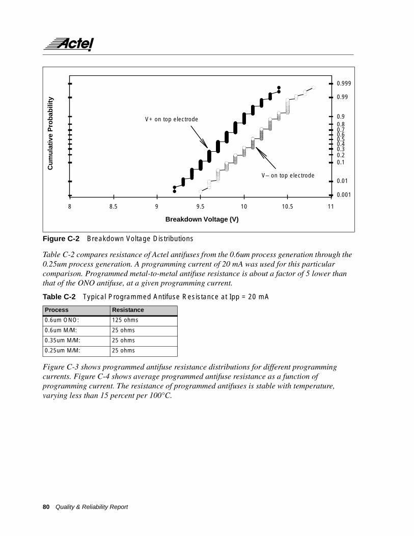
Table C-2 compares resistance of Actel antifuses from the 0.6um process generation through the 0.25um process generation. A programming current of 20 mA was used for this particular comparison. Programmed metal-to-metal antifuse resistance is about a factor of 5 lower than that of the ONO antifuse, at a given programming current.
Figure C-3 shows programmed antifuse resistance distributions for different programming currents. Figure C-4 shows average programmed antifuse resistance as a function of programming current. The resistance of programmed antifuses is stable with temperature, varying less than 15 percent per 100°C.
Figure C-2 Breakdown Voltage Distributions
Table C-2 Typical Programmed Antifuse Resistance at Ipp = 20 mA
Process Resistance
0.6um ONO: 125 ohms
0.6um M/M: 25 ohms
0.35um M/M: 25 ohms
0.25um M/M: 25 ohms
Breakdown Voltage (V)
8 8.5 9.5 10.5 119 10
0.999
0.99
0.9
0.001
0.01
0.10.20.30.40.50.60.70.8
V+ on top electrode
Cu
mu
lati
ve P
rob
abili
ty
V– on top electrode
80 Quality & Reliability Report

Figure C-3 Programmed Antifuse Resistance Distributions
Figure C-4 Antifuse Resistance vs. Programming Current
On-state Resistance (Ohms)
0 10 20 30 40 50 60 70 80
Ipp= 2 5 m A 2 0 m A 15 mA 10 m A
Cu
mu
lati
ve P
rob
abili
ty
0.999
0.99
0.9
0.001
0.01
0.10.20.30.40.50.60.70.8
RonC1
IPP
C2
IPP
= + 2
IPP (mA)
On
-sta
te R
esis
tan
ce (
Oh
ms)
0
20
40
60
80
100
0 5 10 15 20 25 30
Quality & Reliability Report 81

Reliability Characterization and Modeling
Unprogrammed AntifusesTwo possible failure modes for unprogrammed amorphous silicon-based antifuses can be considered:
1 Increase in leakage over time, leading to high standby Idd
2 Breakdown (unintentional programming), leading to functional failure
Both of these failure modes have been characterized in highly accelerated testing of single antifuses and antifuse arrays. Failure is accelerated by applying high voltage and/or high temperature to the test structures. Figure C-5 shows time-to-breakdown distributions at various stress voltages.
We have found that for our dielectric/amorphous silicon antifuse, leakage current increase at normal stress voltages is not a concern for our product. In order to demonstrate this, we have examined the use of 1 and 10 nA per antifuse at 3.6 V as the failure criterion, as well as a failure criterion for dielectric-like breakdown of 1.0 mA at 3.6V.
Additionally, we have found that a 1/E model is an adequate and conservative way to model time to failure over the range of interest (between 0.1 second and 20 years).
Figure C-5 Time-to-Breakdown Distributions
Time (sec)
Cu
mu
lati
ve P
rob
abili
ty
1E + 00 1E + 01 1E + 02 1E + 03 1E + 04 1E + 05 1E + 06
Vstress = 8.5V 8.0V 7.5V 7.0V
0.99
0.950.9
0.01
0.050.1
0.20.30.40.50.60.70.8
82 Quality & Reliability Report

Figure C-6 and Figure C-7 show the median time-to-fail versus 1/V for single antifuses with positive voltage stress on the top electrode and ambient temperatures of 25°C and 150°C, respectively.
Figure C-6 Time to Breakdown vs. 1/V, 25°C
Figure C-7 Time to Breakdown vs. 1/V, 150°C
1/V (1/V)
MT
TF
(se
c)
1E + 10
1E + 09
1E + 08
1E + 07
1E + 06
1E + 05
1E + 04
1E + 03
1E + 02
1E + 01
1E + 00
0.1 0.15 0.2 0.25 0.3
Model
1mA criterion (breakdown)
10nA criterion
1nA criterion
Single antifuseStress polarity: Positive on top electrodeTa = 25°C
1/V (1/V)
MT
TF
(se
c)
1E + 10
1E + 09
1E + 08
1E + 07
1E + 06
1E + 05
1E + 04
1E + 03
1E + 02
1E + 01
1E + 00
0.1 0.15 0.2 0.25 0.3
Single antifuseStress polarity: Positive on top electrodeTa = 25°C
1mA criterion (breakdown)
10nA criterion
1nA criterion
Quality & Reliability Report 83

Figure C-8 shows the median time-to-fail for single antifuses and 1000-antifuse arrays with positive voltage stress on the top electrode at an ambient temperature of 150°C. Failure criterion is breakdown.
The results in Figure C-9 show the dependence of off-state lifetime as a function of ambient temperature. Activation energy for off-state lifetime can be determined using an Arrhenius model for the temperature dependence. The value of the activation energy is approximately 0.3 eV.
Figure C-8 Time-to-Breakdown vs. 1/V, Single Antifuses and 1000-antifuse Arrays
Figure C-9 Time-to-Breakdown vs. 1/T
Med
ian
-tim
e-to
-fai
l (se
c)
1K array
Single antifuse
1/V (1/V)
1E + 10
1E + 09
1E + 08
1E + 07
1E + 06
1E + 05
1E + 04
1E + 03
1E + 02
1E + 01
1E + 00
0.1 0.15 0.2 0.25 0.3
Stress polarity: Positive on top electrodeTa = 150°C1mA criterion (breakdown)
Med
ian
-tim
e-to
-fai
l (se
c)
1000/T (1/K)
51 1.5 2 2.5 3 3.5 4 4.5
Stress Voltage = 7.5V
1E + 06
1E + 05
1E + 04
1E + 03
1E + 02
1E + 01
1E + 00
84 Quality & Reliability Report

Thus a conservative model for failure of unprogrammed Actel antifuses is
t50 = A*exp(-G*V)exp(Ea/kT)
where G depends on film thickness
Ea ~ 0.3
Programmed AntifusesProgrammed amorphous silicon-based metal-to-metal antifuses can be caused to fail by applying a high AC read current. The failure mechanism is similar to metal line electromigration, although here the current acceleration is much more significant than ambient temperature acceleration. Figure C-10 shows programmed antifuse time-to-failure distributions at several different stress currents. The stress used is a 1 MHz AC signal at an ambient temperature of 25°C.
Figure C-11 shows programmed antifuse (on-state) lifetime as a function of programming current and stress current. The median time-to-fail datapoints above 1E7 seconds are extrapolated using the observed log-normal sigma.
Figure C-10 Time-to-failure Distributions
Cu
mu
lati
ve P
rob
abili
ty
Istress = 18.5 mAProgramming Current = 25 mA
Time (sec)
1E + 00 1E + 02 1E + 03 1E + 051E + 04 1E + 06 1E + 07 1E + 08
0.99
0.950.9
0.01
0.050.1
0.20.30.40.50.60.70.8
17.0 mA
18.0 mA
Quality & Reliability Report 85

The model used for on-state lifetime is
t50 = Aexp(Ea/kTmax)
where
Ea ~ 2 eVTmax is not the ambient temperature, but rather the maximum temperature in the antifuse link.
Tmax = Ta + I2 * Rfuse * Theta
I is the stress current
Rfuse is the antifuse resistance (also temperature-dependent)
Theta is the thermal resistance of the link.
We have seen that time to failure in programmed antifuses is only weakly dependent on ambient temperature, but strongly dependent on stress current, as expected. Figure C-12 shows median-time-to fail vs. peak stress current for two different temperatures: 25°C and 125°C. Frequency, waveform, and duty cycle of the stress pulses can also have some effect.
Figure C-11 Time-to-Failure vs. Stress Current
Peak stress current (mA)
Med
ian
-tim
e-to
-fai
l (se
c)
0 5 10 15 20 25 30
25 mA15 mA10 mAIPP = 5 mA
Experiment:Model:1 MHz, AC stressTa = 25°C
1E + 10
1E + 12
1E + 08
1E + 06
1E + 04
1E + 02
1E + 00
86 Quality & Reliability Report

Designing for Reliability
Unprogrammed AntifusesDuring normal operation, voltage across unprogrammed antifuses is limited to VCCA, the array VCC. For example this is a maximum continuous voltage of 3.6V for 0.35um process parts, and 2.8V for 0.25um process parts. I/Os may operate at higher voltages but the antifuses are isolated from them.
A relatively high ratio of programming voltage to operating voltage (VPP/VCCA) is used to ensure that leakage conforms to data sheet standby Idd limits over a 20-year lifetime, and so that low breakdown antifuses can be screened out during final test using a special screen.
Programmed AntifusesThe design of the programming path ensures that the programming current is sufficient to create a robust antifuse link.
The programming algorithm, a function of both the product circuitry and the programming hardware, is optimized to minimize programming time, minimize programmed antifuse resistance, and maximize reliability.
From statistical analysis of data on time-to-failure of programmed antifuses, a safe operating area for stress current at a given programming current has been defined. The product operates within this area for the worst-case process, programming path, and the worst conceivable customer designs.
Figure C-12 Time-to-Failure vs. Stress Current For Different Ambient Temperatures
0 5 10 15 20 25
Ta = 125°C 25°C
Med
ian
-tim
e-to
-fai
l (se
c)
1E + 10
1E + 12
1E + 08
1E + 06
1E + 04
1E + 02
1E + 00
Experiment:Eyring Model:1 MHz, AC stressIPP = 25 mA
Quality & Reliability Report 87

Process Monitoring for Reliability
Unprogrammed AntifusesDuring electrical test (e-test) for wafer and lot acceptance, several antifuse parameters are datalogged in addition to the standard CMOS process parameters. These include:
Breakdown voltages for single antifuses and arrays, for both polarities
Antifuse array leakage at several voltages, for both polarities
Antifuse array capacitance
Leakage after a high-voltage, 1 second screen on a large antifuse array, for both polarities.
These tests can catch process problems and provide a basis for rejecting defective wafers or lots.
Programmed AntifusesThe following are also monitored as part of wafer/lot acceptance:
Programmed antifuse resistance
Threshold voltages and saturation current for high-voltage (programming) transistors.
Product Screening for Reliability
Unprogrammed AntifusesDuring wafer sort and final test operations, all antifuses on every product are subjected to high-voltage screens, designed to weed out parts which could fail during normal operation over the life of the part. Each of these “antifuse stress” screens is on the order of twice the normal VCC, for a duration of about 0.1 seconds.
The data from the pair of screens is used in two ways: First, if an antifuse fails during the screen (detected by leakage in a special test mode), the die or assembled part will be rejected. Second, data from both screens is used to give some resolution of the shape of the unprogrammed antifuse breakdown distribution, and criteria are in place that provide a basis for rejecting wafers or lots based on the results of these screens.
Programmed AntifusesSince antifuse-based FPGAs are one-time programmable, any reliability screen done for programmed antifuses must be done at the time of programming.
We have found that there is a high correlation between initial programmed antifuse resistance and subsequent on-state reliability. Thus if the resistance of an antifuse is too high after programming, the part will be rejected as a programming failure.
88 Quality & Reliability Report
In practice an indication of the antifuse resistance is obtained during product programming, by monitoring current through each antifuse at reduced voltages, after it is programmed. This is done automatically by the programming hardware and software. If an antifuse can not be programmed to a suitably low resistance, the part will be rejected as a programming failure. Other infant mortality failure mechanisms such as gate oxide breakdown or open vias may also cause the part to be rejected as a programming failure.
Product Testing for ReliabilityProduct-level testing for reliability includes process/product qualification testing, ongoing reliability testing, and QA monitors. In addition, more severe engineering characterization of products has been done and is ongoing.
Unprogrammed AntifusesThe standard qualification test that is most indicative of unprogrammed antifuse reliability is the High-Temperature Operating Life (HTOL) test. For 3.3V (VCCA) SX products, the test condition is
VCCA = 4.0 V
Ta = 125°C
Duration = 1000 hours
Based on our model for voltage and temperature acceleration of failure of worst-case unprogrammed antifuses, this test condition provides an acceleration factor in excess of 200x relative to an operating condition of VCCA = 3.6V, Tj = 100C.
The HTOL test is also an effective way to accelerate other failure mechanisms such as gate oxide breakdown, metal line electromigration, mobile ionic contamination degradation.
In addition to the initial qual testing, Actel’s Ongoing Reliability Testing (O.R.T.) program provides for continuing HTOL testing on a sample basis.
Programmed AntifusesFailure in Actel programmed metal-to-metal antifuses is strongly dependent on the stress current going through the programmed antifuses, and only weakly dependent on the ambient temperature. Thus the best way to accelerate failure in programmed antifuses is to do a high-VCC, low-temperature dynamic burn-in. Both the high VCC and low temperature increase the peak stress current going through the antifuse. Our qualification test condition for this Low-Temperature Operating Life (LTOL) Test is
VCCA = 4.0 V
Ta = –55°C
Duration = 1000 hours
Quality & Reliability Report 89
Based on our model for current acceleration of failure of worst-case programmed antifuses, this test condition provides an acceleration factor in excess of 200x relative to an operating condition of VCCA = 3.6V, Tj = 0°C.
In addition to the functional testing done at each time point, the special burn-in designs used in this test allow us to catch transient failures that might occur in between the functional testing time points. Parts under test are continuously monitored for transient failure of programmed antifuses.
The LTOL test is also an effective way to accelerate degradation and failure associated with hot-carrier effects.
As with the HTOL test, sample LTOL testing is done as part of Actel’s Ongoing Reliability Testing (O.R.T.) program.
ConclusionAssuring reliability of Actel Metal-to-Metal antifuse-based Field-Programmable Gate Arrays is a multifaceted task that starts with process design and product architecture. It involves special wafer and lot acceptance criteria, as well as product-level screens designed to identify and discard any products that would fail during normal operating conditions. Qual test conditions and burn-in designs are optimized to catch antifuse-related failures in addition to the standard CMOS process failure modes. Quality is assured by ongoing reliability testing.
Product reliability data can be found in SX product family reliability reports.
References[1] C. Shih, R. Lambertson, F. Hawley, F. Issaq, J. McCollum, E. Hamdy, H. Sakurai, H.
Yuasa, H. Honda, T. Yamaoka, T. Wada, C. Hu, “Characterization and Modeling of a Highly Reliable Metal-to-Metal Antifuse for High-Performance and High-Density Field-Programmable Gate Arrays” in Proceedings of 1997 Reliability Physics Symposium, pp. 25–33, 1997.
[2] S. Chiang, R. Foruohi, W. Chen, F. Hawley, J. McCollum, E. Hamady, and C. Hu, “Antifuse Structure Comparison for Field Programmable Gate Arrays,” IEEE IEDM Tech. Dig., pp. 611–614, 1992.
[3] C. Hu, “Interconnect Devices for Field Programmable Gate Array,” IEEE IEDM Tech. Dig., pp. 591–594, 1992.
[4] S. Cohen, A. Soares, E. Gleason, P. Wyatt, and J. Raffel, “A Novel Metal-Insulator-Metal Structure for Field-Programmable Devices,” IEEE Trans. Electron Devices, Vol. 40, pp. 1277–1283, 1993.
[5] K. Gordon and R. Wong, “Conducting Filament of the Programmed Metal Electrode Amorphous Silicon Antifuse,” IEEE IEDM Tech. Dig., pp. 27–30, 1993.
90 Quality & Reliability Report

Quality & Reliability Report 91
[6] M. Takagi, I. Yoshii, N. Ikeda, H. Yasuda, and K. Hama, “A Highly Reliable Metal-to-Metal Antifuse for High-Speed Field Programmable Gate Arrays,” IEEE IEDM Tech. Dig., pp. 31–34, 1993.
[7] K. Ravindhran, L. Vines, R. Jhota, T. Han, and B. Bhushan, “Field Programmable Gate Array (FPGA) Process Design for Multilevel Metallization Technology,” in Proceedings of 1993 VMIC Conference, pp. 62–64.
[8] Y. Tamura and H. Shinriki, “Most Promising Metal-to-Metal Antifuse based 10nm-thick p-SiNx film for High Density and High Speed FPGA Application,” IEEE IEDM Tech. Dig., pp. 285–288, 1994.
[9] R. Wong and K. Gordon, “Reliability Mechanism of the Unprogrammed Amorphous Silicon Antifuse,” in Proceedings of 1994 Reliability Physics Symposium, pp. 378–382, 1994.
[10] P. Nicollian and W. Hunter, “Model for the Leakage Instability in Unprogrammed Amorphous Silicon Antifuse Devices,” in Proceedings of IEEE Reliability Physics Symposium, pp. 42–47, 1995.
[11] H. Yasuda, N. Ideda, K. Hama, M. Takagi, and I. Yoshii, “Relation Between Stress-Induced Leakage Current and Dielectric Breakdown in SiN-based Antifuses,” in Proceedings of IEEE Reliability Physics Symposium, pp. 225–231, 1994.
[12] G. Zhang, C. Hu, P.Yu, S. Chiang, S. Eltoukhy, and E. Hamdy, “Reliable Metal-to-Metal Oxide Antifuses,” IEEE IEDM Tech. Dig., pp. 281–284, 1994.
[13] Y. Tamura and H. Shinriki, “ON-state, Programming and OFF-state Reliability of Metal-to-Metal Antifuse based 10 nm-thick SiNx film for 3.3 V Operation,” in Proceedings of IEEE Reliability Physics Symposium, pp. 36–41, 1995.
[14] US Patent number: 5,181,096.
[15] G. Zhang, C. Hu, Y. Yu, S. Chiang, S. Eltoukhy, and E. Hamdy, “An Electro-Thermal Model for Metal-Oxide-Metal Antifuses,” IEEE Trans. Electron Devices, vol. 42, pp. 1548–1558, 1995.
[16] G. Zhang, C. Hu, P. Yu, S. Chiang, and E. Hamdy, “Characteristic voltage of the programmed metal-to-metal antifuses,” IEEE Electron Device Lett., vol. 13, pp. 166–168, 1994.
[17] D. Crook, “Method of Determining Reliability Screens for Time Dependent Dielectric Breakdown,” in Proceedings of IEEE Reliability Physics Symposium, pp. 1–7, 1979.
[18] E. Anolick and G. Nelson, “Low Field Time Dependent Dielectric Breakdown,” in Proceedings of IEEE Reliability Physics Symposium, pp.8–12, 1979.
[19] I. Chen, S. Holland, and C. Hu, “A Quantitative Physical Model for Time-Dependent Breakdown in SiO2,” in Proceedings of IEEE Reliability Physics Symposium, pp. 24–31, 1985.
[20] G. Zhang, Y. King, S. Eltoukhy, E. Hamdy, T. Jing, P. Yu, and C. Hu, “On-state Reliability of Amorphous Silicon Antifuses,” IEEE IEDM Tech. Dig., pp. 551–554, 1995.

Actel and the Actel logo are registered trademarks of Actel Corporation.
All other trademarks are the property of their owners.
http://www.actel.com
Actel Europe Ltd.Maxfli Court, Riverside WayCamberly, Surrey GU15 3YLUnited KingdomTel: +44 (0)1276 401450Fax: +44 (0)1276 401490
Actel Corporation955 East Arques AvenueSunnyvale, California 94086USATel: (408) 739-1010Fax: (408) 739-1540
Actel Asia-PacificEXOS Ebisu Bldg. 4F1-24-14 Ebisu Shibuya-kuTokyo 150 JapanTel: +81-(0)3-3445-7671Fax: +81-(0)3-3445-7668
5172060-2/3.01


![[XLS] · Web view2001 2 2003 4 2004 1 2006 1 1995 1 1990 1993 1998 1999 1999 1999 1999 2000 2000 2000 2000 2000 2001 2001 2001 2001 2001 2001 2001 2001 2001 2001 2001 2001 2001 2002](https://static.fdocuments.us/doc/165x107/5bdc2d6f09d3f2bc1c8d6ace/xls-web-view2001-2-2003-4-2004-1-2006-1-1995-1-1990-1993-1998-1999-1999-1999.jpg)