Quad high-side smart power solid-state relay · This is information on a product in full...
25
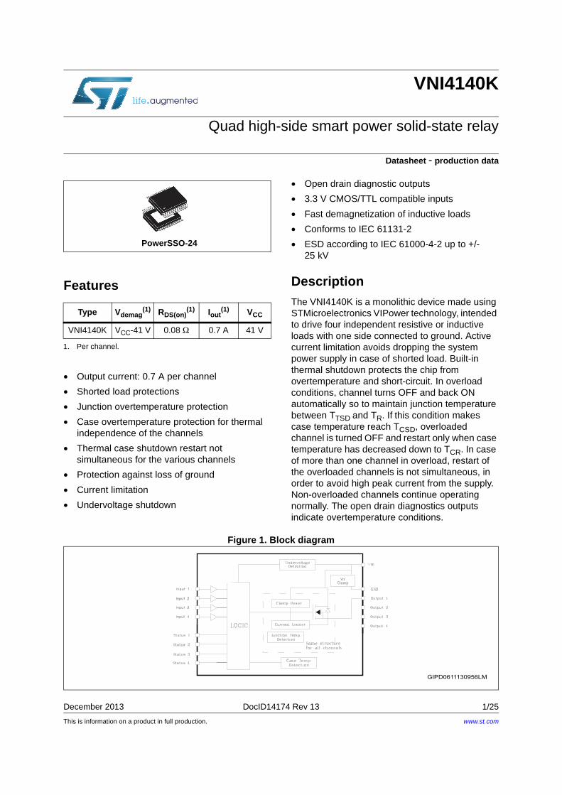
This is information on a product in full production. December 2013 DocID14174 Rev 13 1/25 VNI4140K Quad high-side smart power solid-state relay Datasheet - production data Features • Output current: 0.7 A per channel • Shorted load protections • Junction overtemperature protection • Case overtemperature protection for thermal independence of the channels • Thermal case shutdown restart not simultaneous for the various channels • Protection against loss of ground • Current limitation • Undervoltage shutdown • Open drain diagnostic outputs • 3.3 V CMOS/TTL compatible inputs • Fast demagnetization of inductive loads • Conforms to IEC 61131-2 • ESD according to IEC 61000-4-2 up to +/- 25 kV Description The VNI4140K is a monolithic device made using STMicroelectronics VIPower technology, intended to drive four independent resistive or inductive loads with one side connected to ground. Active current limitation avoids dropping the system power supply in case of shorted load. Built-in thermal shutdown protects the chip from overtemperature and short-circuit. In overload conditions, channel turns OFF and back ON automatically so to maintain junction temperature between T TSD and T R . If this condition makes case temperature reach T CSD , overloaded channel is turned OFF and restart only when case temperature has decreased down to T CR . In case of more than one channel in overload, restart of the overloaded channels is not simultaneous, in order to avoid high peak current from the supply. Non-overloaded channels continue operating normally. The open drain diagnostics outputs indicate overtemperature conditions. Figure 1. Block diagram Type V demag (1) 1. Per channel. R DS(on) (1) I out (1) V CC VNI4140K V CC -41 V 0.08 Ω 0.7 A 41 V PowerSSO-24 GIPD0611130956LM www.st.com
-
Upload
duongtuyen -
Category
Documents
-
view
215 -
download
0
Transcript of Quad high-side smart power solid-state relay · This is information on a product in full...
This is information on a product in full production.
December 2013 DocID14174 Rev 13 1/25
VNI4140K
Quad high-side smart power solid-state relay
Datasheet - production data
Features
• Output current: 0.7 A per channel
• Shorted load protections
• Junction overtemperature protection
• Case overtemperature protection for thermal independence of the channels
• Thermal case shutdown restart not simultaneous for the various channels
• Protection against loss of ground
• Current limitation
• Undervoltage shutdown
• Open drain diagnostic outputs
• 3.3 V CMOS/TTL compatible inputs
• Fast demagnetization of inductive loads
• Conforms to IEC 61131-2
• ESD according to IEC 61000-4-2 up to +/- 25 kV
DescriptionThe VNI4140K is a monolithic device made using STMicroelectronics VIPower technology, intended to drive four independent resistive or inductive loads with one side connected to ground. Active current limitation avoids dropping the system power supply in case of shorted load. Built-in thermal shutdown protects the chip from overtemperature and short-circuit. In overload conditions, channel turns OFF and back ON automatically so to maintain junction temperature between TTSD and TR. If this condition makes case temperature reach TCSD, overloaded channel is turned OFF and restart only when case temperature has decreased down to TCR. In case of more than one channel in overload, restart of the overloaded channels is not simultaneous, in order to avoid high peak current from the supply. Non-overloaded channels continue operating normally. The open drain diagnostics outputs indicate overtemperature conditions.
Figure 1. Block diagram
Type Vdemag(1)
1. Per channel.
RDS(on)(1) Iout
(1) VCC
VNI4140K VCC-41 V 0.08 Ω 0.7 A 41 V
PowerSSO-24
GIPD0611130956LM
www.st.com
Contents VNI4140K
2/25 DocID14174 Rev 13
Contents
1 Pin connection . . . . . . . . . . . . . . . . . . . . . . . . . . . . . . . . . . . . . . . . . . . . . . 3
2 Maximum ratings . . . . . . . . . . . . . . . . . . . . . . . . . . . . . . . . . . . . . . . . . . . . 5
2.1 Thermal data . . . . . . . . . . . . . . . . . . . . . . . . . . . . . . . . . . . . . . . . . . . . . . . 5
3 Electrical characteristics . . . . . . . . . . . . . . . . . . . . . . . . . . . . . . . . . . . . . 6
4 Truth table . . . . . . . . . . . . . . . . . . . . . . . . . . . . . . . . . . . . . . . . . . . . . . . . . 9
5 Typical application circuit . . . . . . . . . . . . . . . . . . . . . . . . . . . . . . . . . . . . 9
6 Switching waveforms . . . . . . . . . . . . . . . . . . . . . . . . . . . . . . . . . . . . . . . 11
7 Pin functions . . . . . . . . . . . . . . . . . . . . . . . . . . . . . . . . . . . . . . . . . . . . . . 12
8 Package and PC board thermal data . . . . . . . . . . . . . . . . . . . . . . . . . . . 14
8.1 VNI4140K thermal data . . . . . . . . . . . . . . . . . . . . . . . . . . . . . . . . . . . . . . 14
9 Reverse polarity protection . . . . . . . . . . . . . . . . . . . . . . . . . . . . . . . . . . 16
10 Demagnetization energy . . . . . . . . . . . . . . . . . . . . . . . . . . . . . . . . . . . . . 17
11 Package mechanical data . . . . . . . . . . . . . . . . . . . . . . . . . . . . . . . . . . . . 18
12 Ordering information . . . . . . . . . . . . . . . . . . . . . . . . . . . . . . . . . . . . . . . 23
13 Revision history . . . . . . . . . . . . . . . . . . . . . . . . . . . . . . . . . . . . . . . . . . . 24
DocID14174 Rev 13 3/25
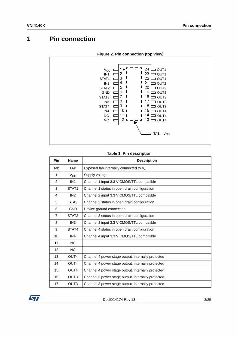
VNI4140K Pin connection
25
1 Pin connection
Figure 2. Pin connection (top view)
Table 1. Pin description
Pin Name Description
Tab TAB Exposed tab internally connected to Vcc
1 VCC Supply voltage
2 IN1 Channel 1 input 3.3 V CMOS/TTL compatible
3 STAT1 Channel 1 status in open drain configuration
4 IN2 Channel 2 input 3.3 V CMOS/TTL compatible
5 STA2 Channel 2 status in open drain configuration
6 GND Device ground connection
7 STAT3 Channel 3 status in open drain configuration
8 IN3 Channel 3 input 3.3 V CMOS/TTL compatible
9 STAT4 Channel 4 status in open drain configuration
10 IN4 Channel 4 input 3.3 V CMOS/TTL compatible
11 NC
12 NC
13 OUT4 Channel 4 power stage output, internally protected
14 OUT4 Channel 4 power stage output, internally protected
15 OUT4 Channel 4 power stage output, internally protected
16 OUT3 Channel 3 power stage output, internally protected
17 OUT3 Channel 3 power stage output, internally protected
OUT1OUT1OUT1OUT2OUT2OUT2
VCCIN1
STAT1IN2
STAT2GND
OUT3OUT3OUT3OUT4OUT4OUT4
STAT3IN3
STAT4
NCNC
IN4
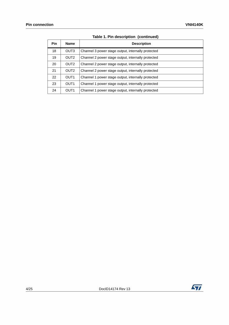
Pin connection VNI4140K
4/25 DocID14174 Rev 13
Pin Name Description
18 OUT3 Channel 3 power stage output, internally protected
19 OUT2 Channel 2 power stage output, internally protected
20 OUT2 Channel 2 power stage output, internally protected
21 OUT2 Channel 2 power stage output, internally protected
22 OUT1 Channel 1 power stage output, internally protected
23 OUT1 Channel 1 power stage output, internally protected
24 OUT1 Channel 1 power stage output, internally protected
Table 1. Pin description (continued)
DocID14174 Rev 13 5/25
VNI4140K Maximum ratings
25
2 Maximum ratings
2.1 Thermal data
Table 2. Absolute maximum ratings
Symbol Parameter Value Unit
VCC Power supply voltage 41 V
-VCC Reverse supply voltage -0.3 V
IGND DC ground reverse current -250 mA
IOUT Output current (continuous) Internally limited A
IR Reverse output current (per channel) -5 A
IIN Input current (per channel) ± 10 mA
VIN Input voltage +VCC V
VSTAT Status pin voltage +VCC V
ISTAT Status pin current ± 10 mA
VESD Electrostatic discharge (R = 1.5 kΩ; C = 100 pF) 2000 V
EAS IOUT = 500 mA TAMB = 125 °C 5 J
PTOT Power dissipation at Tc = 25 °C Internally limited W
TJ Junction operating temperature Internally limited °C
TSTG Storage temperature -55 to 150 °C
Table 3. Thermal data
Symbol Parameter Value Unit
Rth(JC) Thermal resistance junction-case (1)
1. Per channel.
Max. 2 °C/W
Rth(JA) Thermal resistance junction-ambient Max. see Figure 11 °C/W
Electrical characteristics VNI4140K
6/25 DocID14174 Rev 13
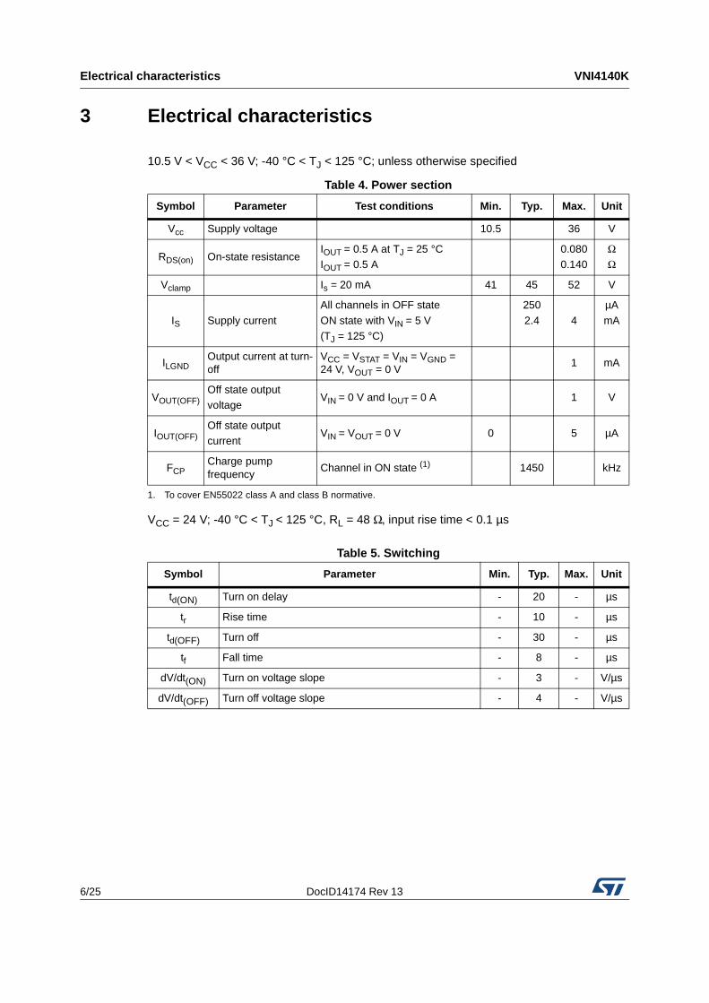
3 Electrical characteristics
10.5 V < VCC < 36 V; -40 °C < TJ < 125 °C; unless otherwise specified
VCC = 24 V; -40 °C < TJ < 125 °C, RL = 48 Ω, input rise time < 0.1 µs
Table 4. Power section
Symbol Parameter Test conditions Min. Typ. Max. Unit
Vcc Supply voltage 10.5 36 V
RDS(on) On-state resistanceIOUT = 0.5 A at TJ = 25 °CIOUT = 0.5 A
0.0800.140
ΩΩ
Vclamp Is = 20 mA 41 45 52 V
IS Supply current
All channels in OFF state
ON state with VIN = 5 V (TJ = 125 °C)
250
2.4 4
µA
mA
ILGNDOutput current at turn-off
VCC = VSTAT = VIN = VGND = 24 V, VOUT = 0 V
1 mA
VOUT(OFF)Off state output voltage
VIN = 0 V and IOUT = 0 A 1 V
IOUT(OFF)Off state output current
VIN = VOUT = 0 V 0 5 µA
FCPCharge pump frequency
Channel in ON state (1)
1. To cover EN55022 class A and class B normative.
1450 kHz
Table 5. Switching
Symbol Parameter Min. Typ. Max. Unit
td(ON) Turn on delay - 20 - µs
tr Rise time - 10 - µs
td(OFF) Turn off - 30 - µs
tf Fall time - 8 - µs
dV/dt(ON) Turn on voltage slope - 3 - V/µs
dV/dt(OFF) Turn off voltage slope - 4 - V/µs
DocID14174 Rev 13 7/25
VNI4140K Electrical characteristics
25
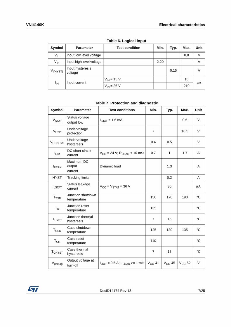
Table 6. Logical input
Symbol Parameter Test condition Min. Typ. Max. Unit
VIL Input low level voltage 0.8 V
VIH Input high level voltage 2.20 V
VI(HYST)Input hysteresis voltage
0.15 V
IIN Input currentVIN = 15 V 10
μΑVIN = 36 V 210
Table 7. Protection and diagnostic
Symbol Parameter Test conditions Min. Typ. Max. Unit
VSTAT Status voltage output low
ISTAT = 1.6 mA 0.6 V
VUSDUndervoltage protection
7 10.5 V
VUSDHYSUndervoltage hysteresis
0.4 0.5 V
ILIMDC short-circuit current
VCC = 24 V; RLOAD < 10 mΩ 0.7 1 1.7 A
IPEAK
Maximum DC output
currentDynamic load 1.3 A
HYST Tracking limits 0.2 A
ILSTATStatus leakage current
VCC = VSTAT = 36 V 30 μΑ
TTSDJunction shutdown temperature
150 170 190 °C
TRJunction reset temperature
135 °C
THYSTJunction thermal hysteresis
7 15 °C
TCSDCase shutdown temperature
125 130 135 °C
TCRCase reset temperature
110 °C
TCHYSTCase thermal hysteresis
7 15 °C
VdemagOutput voltage at
turn-offIOUT = 0.5 A; LLOAD >= 1 mH VCC-41 VCC-45 VCC-52 V
Electrical characteristics VNI4140K
8/25 DocID14174 Rev 13
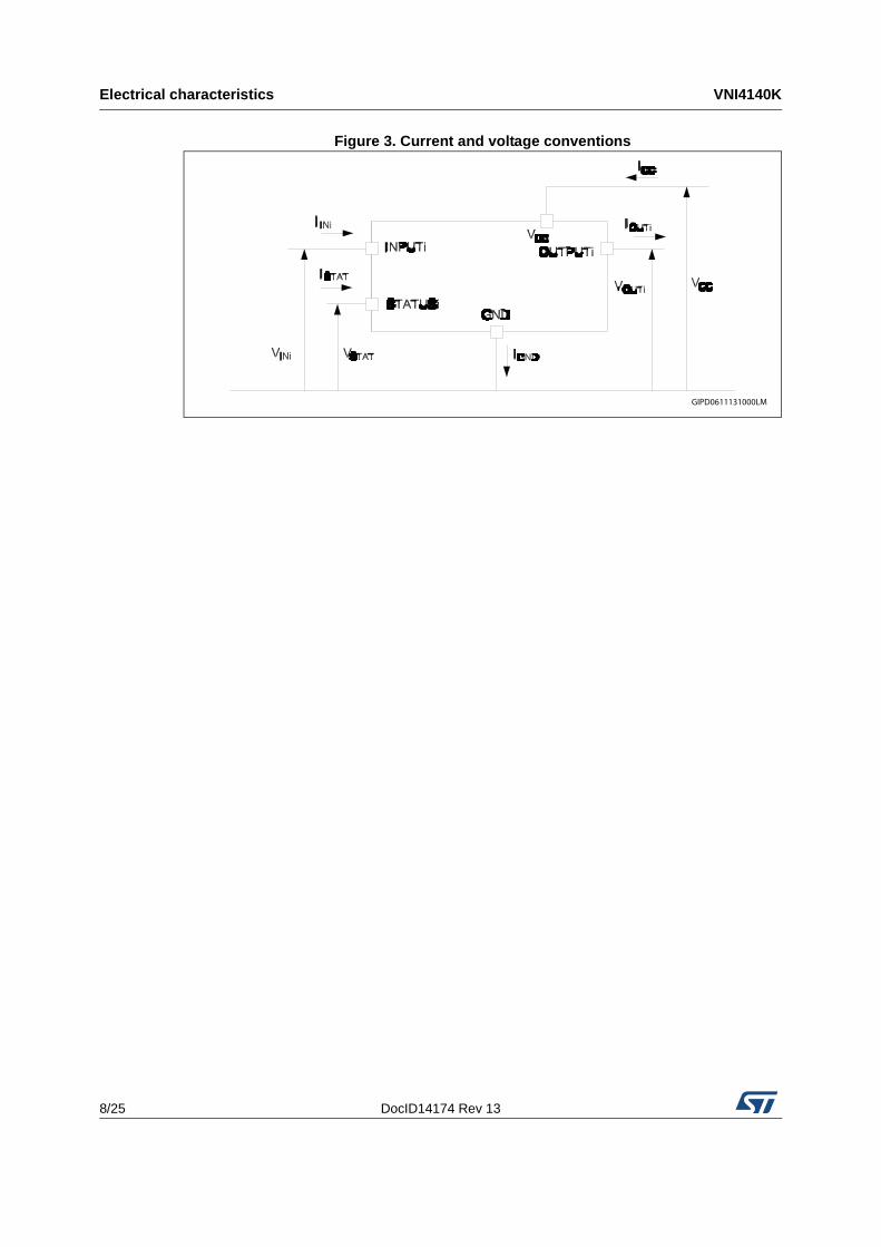
Figure 3. Current and voltage conventions
GIPD0611131000LM
DocID14174 Rev 13 9/25
VNI4140K Truth table
25
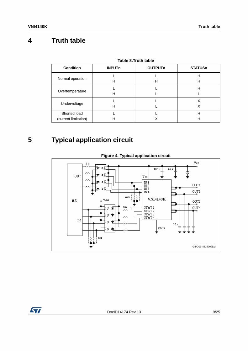
4 Truth table
5 Typical application circuit
Figure 4. Typical application circuit
Table 8.Truth table
Condition INPUTn OUTPUTn STATUSn
Normal operationLH
LH
HH
OvertemperatureLH
LL
HL
UndervoltageLH
LL
XX
Shorted load(current limitation)
LH
LX
HH
GIPD0611131009LM
Typical application circuit VNI4140K
10/25 DocID14174 Rev 13
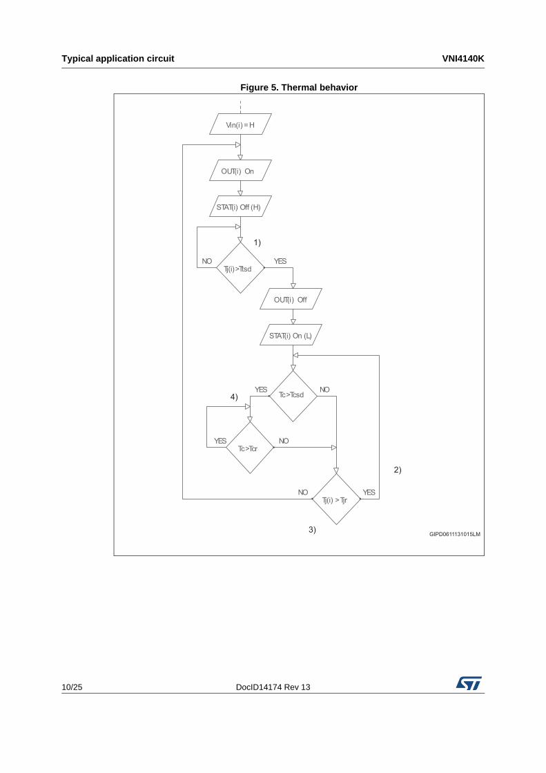
Figure 5. Thermal behavior
NOTj(i) > Ttsd
Vin(i) = H
OUT(i) Off
STAT(i) On (L)
Tc > Tcsd
NO
YES
NOYES
Tc > TcrYES
NOTj(i) > Tjr
YES
STAT(i) Off (H)
OUT(i) On
1)
4)
2)
3)GIPD0611131015LM
DocID14174 Rev 13 11/25
VNI4140K Switching waveforms
25
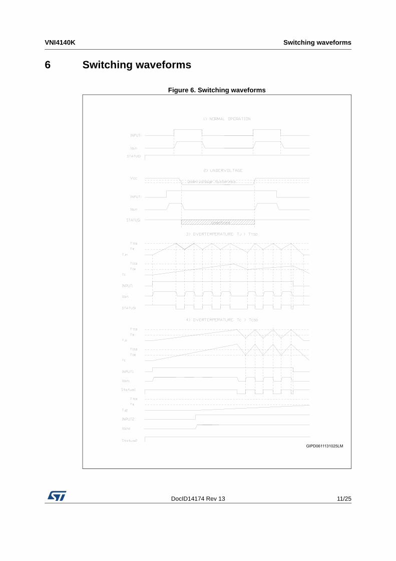
6 Switching waveforms
Figure 6. Switching waveforms
GIPD0611131025LM
Pin functions VNI4140K
12/25 DocID14174 Rev 13
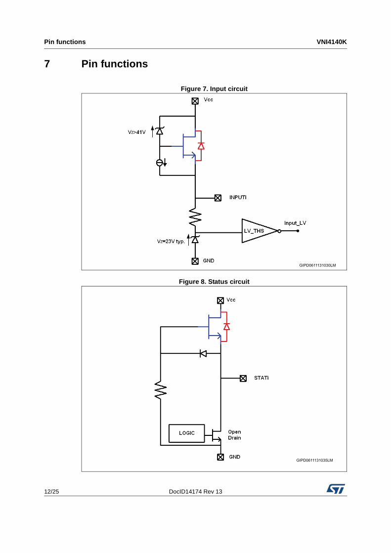
7 Pin functions
Figure 7. Input circuit
Figure 8. Status circuit
GIPD0611131030LM
GIPD0611131035LM
DocID14174 Rev 13 13/25
VNI4140K Pin functions
25
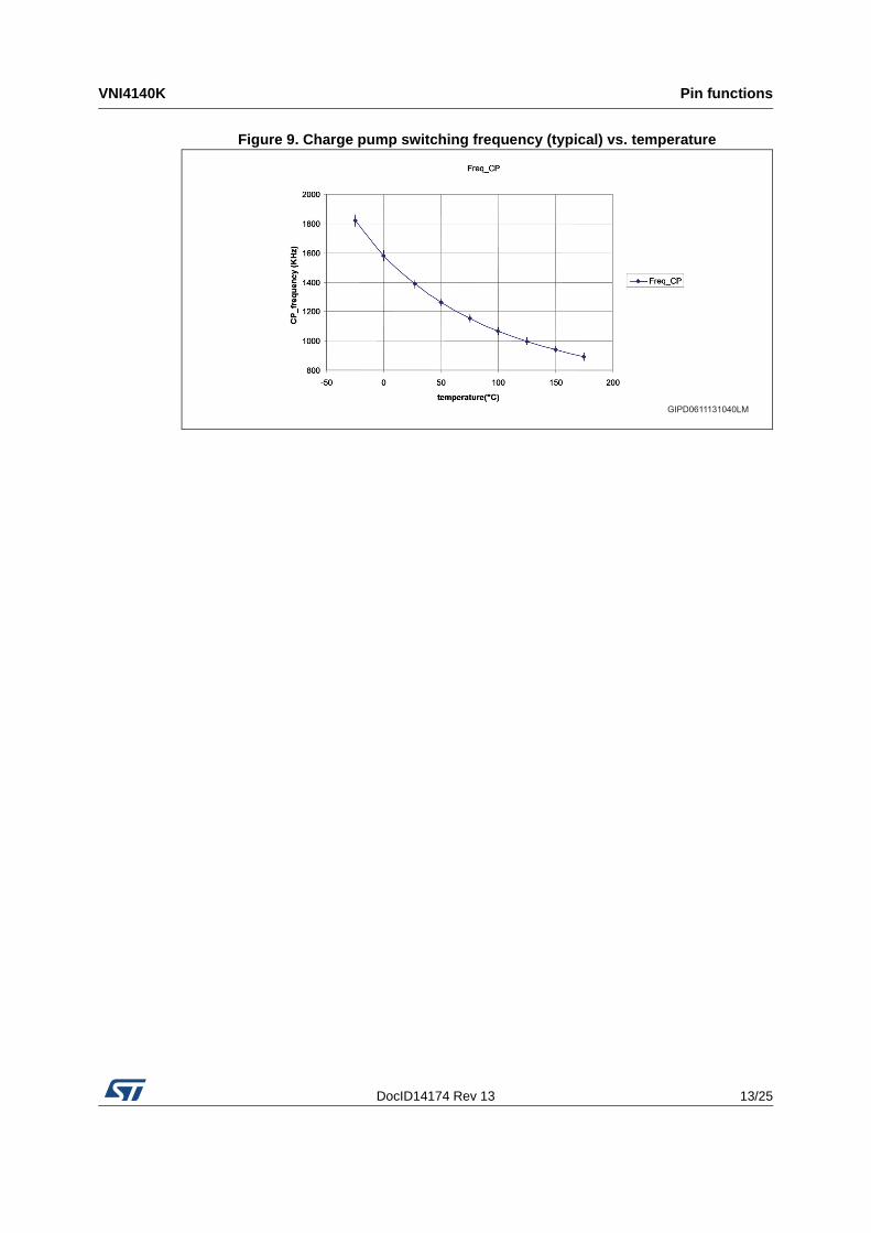
Figure 9. Charge pump switching frequency (typical) vs. temperature
GIPD0611131040LM
Package and PC board thermal data VNI4140K
14/25 DocID14174 Rev 13
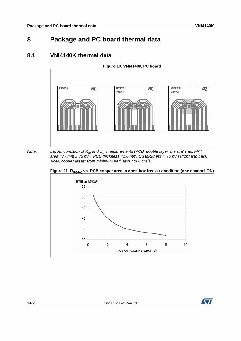
8 Package and PC board thermal data
8.1 VNI4140K thermal data
Figure 10. VNI4140K PC board
Note: Layout condition of Rth and Zth measurements (PCB: double layer, thermal vias, FR4 area =77 mm x 86 mm, PCB thickness =1.6 mm, Cu thickness = 70 mm (front and back side), copper areas: from minimum pad layout to 8 cm2).
Figure 11. Rth(JA) vs. PCB copper area in open box free air condition (one channel ON)
DocID14174 Rev 13 15/25
VNI4140K Package and PC board thermal data
25
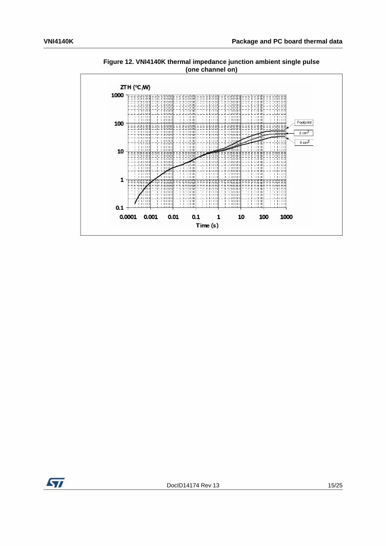
Figure 12. VNI4140K thermal impedance junction ambient single pulse (one channel on)
Reverse polarity protection VNI4140K
16/25 DocID14174 Rev 13
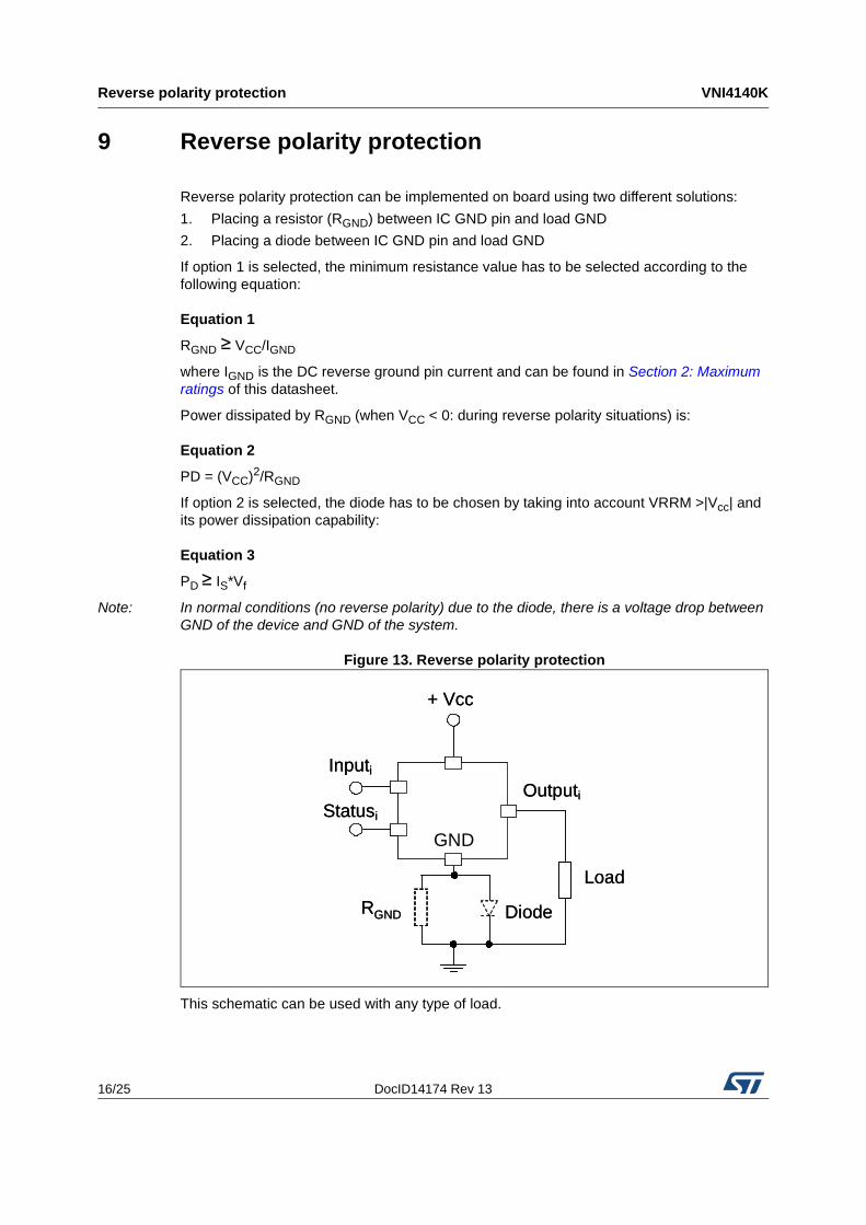
9 Reverse polarity protection
Reverse polarity protection can be implemented on board using two different solutions:
1. Placing a resistor (RGND) between IC GND pin and load GND
2. Placing a diode between IC GND pin and load GND
If option 1 is selected, the minimum resistance value has to be selected according to the following equation:
Equation 1
RGND ≥ VCC/IGND
where IGND is the DC reverse ground pin current and can be found in Section 2: Maximum ratings of this datasheet.
Power dissipated by RGND (when VCC < 0: during reverse polarity situations) is:
Equation 2
PD = (VCC)2/RGND
If option 2 is selected, the diode has to be chosen by taking into account VRRM >|Vcc| and its power dissipation capability:
Equation 3
PD ≥ IS*Vf
Note: In normal conditions (no reverse polarity) due to the diode, there is a voltage drop between GND of the device and GND of the system.
Figure 13. Reverse polarity protection
This schematic can be used with any type of load.
Statusi
Inputi
GND
Outputi
+ Vcc
RGND
Load
Diode
Statusi
Inputi
GND
Outputi
+ Vcc
RGND
Load
Diode
DocID14174 Rev 13 17/25
VNI4140K Demagnetization energy
25
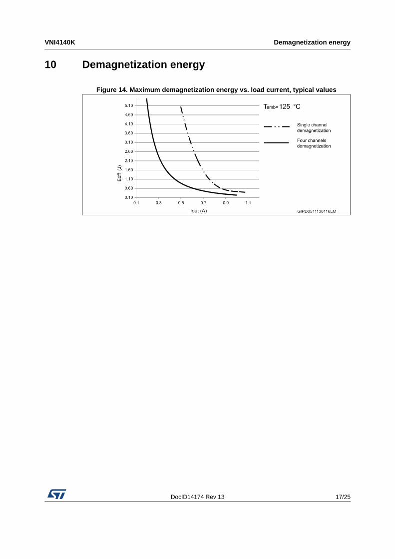
10 Demagnetization energy
Figure 14. Maximum demagnetization energy vs. load current, typical values
0.10
0.60
1.10
1.60
2.10
2.60
3.10
3.60
4.10
4.60
5.10
0.1 0.3 0.5 0.7 0.9 1.1
Single channeldemagnetization
Four channelsdemagnetization
Iout (A)
Eoff
(J)
Tamb=125 °C
GIPD0511130116LM
Package mechanical data VNI4140K
18/25 DocID14174 Rev 13
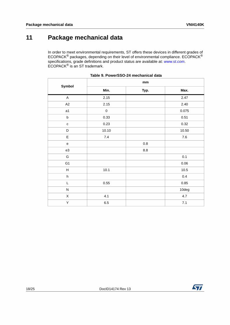
11 Package mechanical data
In order to meet environmental requirements, ST offers these devices in different grades of ECOPACK® packages, depending on their level of environmental compliance. ECOPACK® specifications, grade definitions and product status are available at: www.st.com. ECOPACK® is an ST trademark.
Table 9. PowerSSO-24 mechanical data
Symbol mm
Min. Typ. Max.
A 2.15 2.47
A2 2.15 2.40
a1 0 0.075
b 0.33 0.51
c 0.23 0.32
D 10.10 10.50
E 7.4 7.6
e 0.8
e3 8.8
G 0.1
G1 0.06
H 10.1 10.5
h 0.4
L 0.55 0.85
N 10deg
X 4.1 4.7
Y 6.5 7.1
DocID14174 Rev 13 19/25
VNI4140K Package mechanical data
25
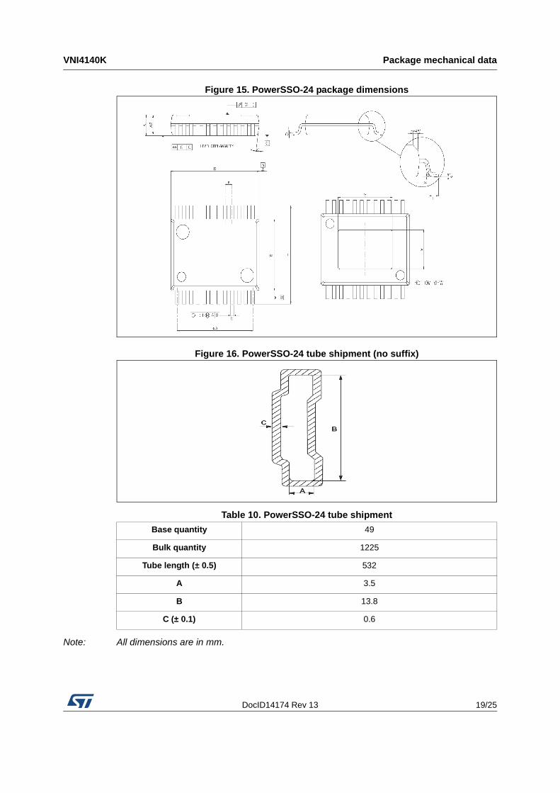
Figure 15. PowerSSO-24 package dimensions
Figure 16. PowerSSO-24 tube shipment (no suffix)
Note: All dimensions are in mm.
Table 10. PowerSSO-24 tube shipment
Base quantity 49
Bulk quantity 1225
Tube length (± 0.5) 532
A 3.5
B 13.8
C (± 0.1) 0.6
Package mechanical data VNI4140K
20/25 DocID14174 Rev 13
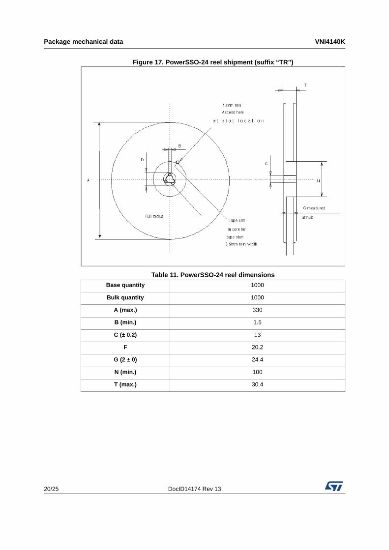
Figure 17. PowerSSO-24 reel shipment (suffix “TR”)
Table 11. PowerSSO-24 reel dimensions
Base quantity 1000
Bulk quantity 1000
A (max.) 330
B (min.) 1.5
C (± 0.2) 13
F 20.2
G (2 ± 0) 24.4
N (min.) 100
T (max.) 30.4
DocID14174 Rev 13 21/25
VNI4140K Package mechanical data
25
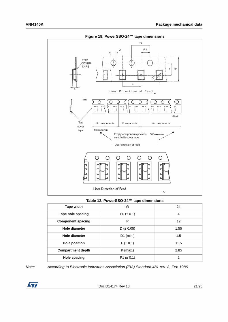
Figure 18. PowerSSO-24™ tape dimensions
Note: According to Electronic Industries Association (EIA) Standard 481 rev. A, Feb 1986
Table 12. PowerSSO-24™ tape dimensions
Tape width W 24
Tape hole spacing P0 (± 0.1) 4
Component spacing P 12
Hole diameter D (± 0.05) 1.55
Hole diameter D1 (min.) 1.5
Hole position F (± 0.1) 11.5
Compartment depth K (max.) 2.85
Hole spacing P1 (± 0.1) 2
Package mechanical data VNI4140K
22/25 DocID14174 Rev 13
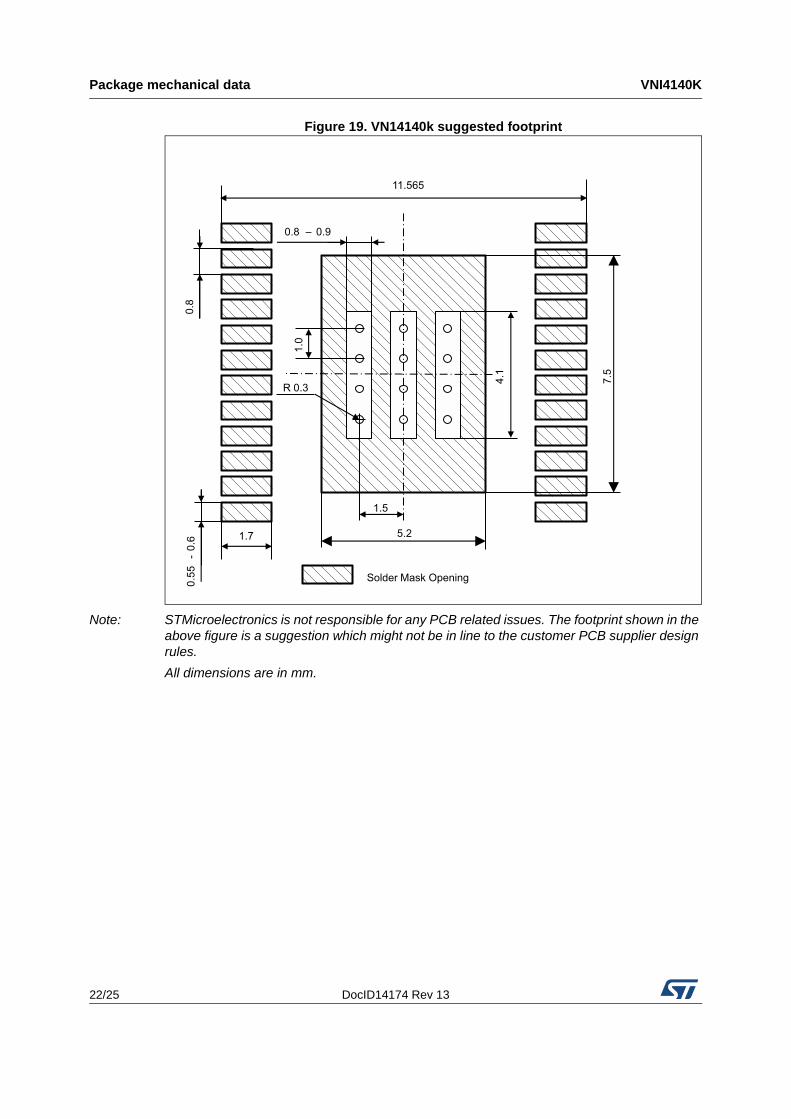
Figure 19. VN14140k suggested footprint
Note: STMicroelectronics is not responsible for any PCB related issues. The footprint shown in the above figure is a suggestion which might not be in line to the customer PCB supplier design rules.
All dimensions are in mm.
DocID14174 Rev 13 23/25
VNI4140K Ordering information
25
12 Ordering information
Table 13. Order code
Order code Package Packaging
VNI4140K PowerSSO-24 Tube
VNI4140KTR PowerSSO-24 Tape and reel
Revision history VNI4140K
24/25 DocID14174 Rev 13
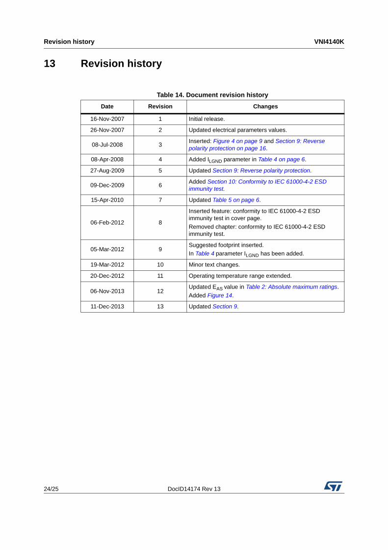
13 Revision history
Table 14. Document revision history
Date Revision Changes
16-Nov-2007 1 Initial release.
26-Nov-2007 2 Updated electrical parameters values.
08-Jul-2008 3Inserted: Figure 4 on page 9 and Section 9: Reverse polarity protection on page 16.
08-Apr-2008 4 Added ILGND parameter in Table 4 on page 6.
27-Aug-2009 5 Updated Section 9: Reverse polarity protection.
09-Dec-2009 6Added Section 10: Conformity to IEC 61000-4-2 ESD immunity test.
15-Apr-2010 7 Updated Table 5 on page 6.
06-Feb-2012 8
Inserted feature: conformity to IEC 61000-4-2 ESD immunity test in cover page.
Removed chapter: conformity to IEC 61000-4-2 ESD immunity test.
05-Mar-2012 9Suggested footprint inserted.In Table 4 parameter ILGND has been added.
19-Mar-2012 10 Minor text changes.
20-Dec-2012 11 Operating temperature range extended.
06-Nov-2013 12Updated EAS value in Table 2: Absolute maximum ratings.
Added Figure 14.
11-Dec-2013 13 Updated Section 9.
DocID14174 Rev 13 25/25
VNI4140K
25
Please Read Carefully:
Information in this document is provided solely in connection with ST products. STMicroelectronics NV and its subsidiaries (“ST”) reserve theright to make changes, corrections, modifications or improvements, to this document, and the products and services described herein at anytime, without notice.
All ST products are sold pursuant to ST’s terms and conditions of sale.
Purchasers are solely responsible for the choice, selection and use of the ST products and services described herein, and ST assumes noliability whatsoever relating to the choice, selection or use of the ST products and services described herein.
No license, express or implied, by estoppel or otherwise, to any intellectual property rights is granted under this document. If any part of thisdocument refers to any third party products or services it shall not be deemed a license grant by ST for the use of such third party productsor services, or any intellectual property contained therein or considered as a warranty covering the use in any manner whatsoever of suchthird party products or services or any intellectual property contained therein.
UNLESS OTHERWISE SET FORTH IN ST’S TERMS AND CONDITIONS OF SALE ST DISCLAIMS ANY EXPRESS OR IMPLIEDWARRANTY WITH RESPECT TO THE USE AND/OR SALE OF ST PRODUCTS INCLUDING WITHOUT LIMITATION IMPLIEDWARRANTIES OF MERCHANTABILITY, FITNESS FOR A PARTICULAR PURPOSE (AND THEIR EQUIVALENTS UNDER THE LAWSOF ANY JURISDICTION), OR INFRINGEMENT OF ANY PATENT, COPYRIGHT OR OTHER INTELLECTUAL PROPERTY RIGHT.
ST PRODUCTS ARE NOT DESIGNED OR AUTHORIZED FOR USE IN: (A) SAFETY CRITICAL APPLICATIONS SUCH AS LIFESUPPORTING, ACTIVE IMPLANTED DEVICES OR SYSTEMS WITH PRODUCT FUNCTIONAL SAFETY REQUIREMENTS; (B)AERONAUTIC APPLICATIONS; (C) AUTOMOTIVE APPLICATIONS OR ENVIRONMENTS, AND/OR (D) AEROSPACE APPLICATIONSOR ENVIRONMENTS. WHERE ST PRODUCTS ARE NOT DESIGNED FOR SUCH USE, THE PURCHASER SHALL USE PRODUCTS ATPURCHASER’S SOLE RISK, EVEN IF ST HAS BEEN INFORMED IN WRITING OF SUCH USAGE, UNLESS A PRODUCT ISEXPRESSLY DESIGNATED BY ST AS BEING INTENDED FOR “AUTOMOTIVE, AUTOMOTIVE SAFETY OR MEDICAL” INDUSTRYDOMAINS ACCORDING TO ST PRODUCT DESIGN SPECIFICATIONS. PRODUCTS FORMALLY ESCC, QML OR JAN QUALIFIED AREDEEMED SUITABLE FOR USE IN AEROSPACE BY THE CORRESPONDING GOVERNMENTAL AGENCY.
Resale of ST products with provisions different from the statements and/or technical features set forth in this document shall immediately voidany warranty granted by ST for the ST product or service described herein and shall not create or extend in any manner whatsoever, anyliability of ST.
ST and the ST logo are trademarks or registered trademarks of ST in various countries.Information in this document supersedes and replaces all information previously supplied.
The ST logo is a registered trademark of STMicroelectronics. All other names are the property of their respective owners.
© 2013 STMicroelectronics - All rights reserved
STMicroelectronics group of companies
Australia - Belgium - Brazil - Canada - China - Czech Republic - Finland - France - Germany - Hong Kong - India - Israel - Italy - Japan - Malaysia - Malta - Morocco - Philippines - Singapore - Spain - Sweden - Switzerland - United Kingdom - United States of America
www.st.com