
QCA6234 Integrated Dual-Band 2x2 802.11n + Bluetooth® 4.0 Data ...
48
Qualcomm Technologies, Inc. © 2015-2016 Qualcomm Technologies, Inc. All rights reserved. Qualcomm Snapdragon is a product of Qualcomm Technologies, Inc. Other Qualcomm products referenced herein are products of Qualcomm Technologies, Inc. or its other subsidiaries. DragonBoard, Qualcomm, and Snapdragon are trademarks of Qualcomm Incorporated, registered in the United States and other countries. Other product and brand names may be trademarks or registered trademarks of their respective owners. This technical data may be subject to U.S. and international export, re-export, or transfer (“export”) laws. Diversion contrary to U.S. and international law is strictly prohibited. Use of this document is subject to the license set forth in Exhibit 1. Qualcomm Technologies, Inc. 5775 Morehouse Drive San Diego, CA 92121 U.S.A. LM80-P0598-12 Rev B QCA6234 Integrated Dual-Band 2x2 802.11n + Bluetooth ® 4.0 Data Sheet LM80-P0598-12 Rev B September 2016
Transcript of QCA6234 Integrated Dual-Band 2x2 802.11n + Bluetooth® 4.0 Data ...

Qualcomm Technologies, Inc.
© 2015-2016 Qualcomm Technologies, Inc. All rights reserved.
Qualcomm Snapdragon is a product of Qualcomm Technologies, Inc. Other Qualcomm products referenced herein are products of Qualcomm Technologies, Inc. or its other subsidiaries.
DragonBoard, Qualcomm, and Snapdragon are trademarks of Qualcomm Incorporated, registered in the United States and other countries. Other product and brand names may be trademarks or registered trademarks of their respective owners.
This technical data may be subject to U.S. and international export, re-export, or transfer (“export”) laws. Diversion contrary to U.S. and international law is strictly prohibited.
Use of this document is subject to the license set forth in Exhibit 1.
Qualcomm Technologies, Inc. 5775 Morehouse Drive San Diego, CA 92121
U.S.A.
LM80-P0598-12 Rev B
QCA6234 Integrated Dual-Band 2x2 802.11n + Bluetooth® 4.0
Data Sheet
LM80-P0598-12 Rev B
September 2016

LM80-P0598-12 Rev B MAY CONTAIN U.S. AND INTERNATIONAL EXPORT CONTROLLED INFORMATION 2
Revision history
Revision Date Description
B September 2016 Update for ‘E’ part
A June 1, 2015 Initial release

LM80-P0598-12 Rev B MAY CONTAIN U.S. AND INTERNATIONAL EXPORT CONTROLLED INFORMATION 3
Contents
1 Introduction ........................................................................................................................... 6
1.1 General description .................................................................................................................................... 6 1.2 Acronyms, abbreviations, and terms .......................................................................................................... 7 1.3 QCA6234 features ..................................................................................................................................... 9
2 Features Summary ...............................................................................................................11
2.1 Overview .................................................................................................................................................. 11 2.2 Radio front end ........................................................................................................................................ 11 2.3 Industry leading coexistence .................................................................................................................... 11 2.4 Power management ................................................................................................................................. 11 2.5 Manufacturing calibration ......................................................................................................................... 12 2.6 Reference frequency ................................................................................................................................ 12 2.7 Internal sleep clock .................................................................................................................................. 12 2.8 Interfaces ................................................................................................................................................. 12 2.9 Mobile 802.11n ........................................................................................................................................ 12 2.10 Advanced WLAN features ...................................................................................................................... 13
2.10.1 AP mode (mobile hot spot) ................................................................................................... 14 2.10.2 Wi-Fi Direct (peer-to-peer) .................................................................................................... 14
2.11 Host offloading (WLAN) ......................................................................................................................... 14 2.12 Advanced Bluetooth ............................................................................................................................... 15
3 WLAN Functional Description .............................................................................................17
3.1 Overview .................................................................................................................................................. 17 3.2 XTENSA CPU .......................................................................................................................................... 17 3.3 AHB and APB blocks ............................................................................................................................... 18 3.4 MBOX ...................................................................................................................................................... 18 3.5 Debug UART ........................................................................................................................................... 18 3.6 Reset control ............................................................................................................................................ 18 3.7 Reset sequence ....................................................................................................................................... 19 3.8 Power transition diagram ......................................................................................................................... 19
3.8.1 Hardware power states ........................................................................................................... 19 3.8.2 Sleep state management ........................................................................................................ 19
3.9 System clocking (RTC block) ................................................................................................................... 21 3.9.1 High-speed clocking ............................................................................................................... 21 3.9.2 Low-speed clocking ................................................................................................................ 21 3.9.3 Interface clock ........................................................................................................................ 22
3.10 MAC/BB/RF block .................................................................................................................................. 22 3.11 Baseband block ..................................................................................................................................... 22 3.12 Design for test ........................................................................................................................................ 22
4 Bluetooth Functional Description .......................................................................................23
4.1 HCI-UART interface ................................................................................................................................. 23 4.2 PCM interface .......................................................................................................................................... 23 4.3 CPU and memory .................................................................................................................................... 23 4.4 Standard WLAN coexistence ................................................................................................................... 23 4.5 QTI proprietary coexistence interface ...................................................................................................... 23 4.6 Reference clock ....................................................................................................................................... 24

QCA6234 Integrated Dual-Band 2x2 802.11n + Bluetooth 4.0 Data Sheet Contents
LM80-P0598-12 Rev B MAY CONTAIN U.S. AND INTERNATIONAL EXPORT CONTROLLED INFORMATION 4
4.7 BT low energy .......................................................................................................................................... 24 4.8 Reset ....................................................................................................................................................... 24 4.9 Radio ....................................................................................................................................................... 24 4.10 GPIO ...................................................................................................................................................... 24
5 Electrical Characteristics ....................................................................................................25
5.1 Absolute maximum ratings ....................................................................................................................... 25 5.2 Recommended operating conditions........................................................................................................ 25 5.3 DC electrical characteristics ..................................................................................................................... 26 5.4 WLAN radio receiver characteristics ........................................................................................................ 28 5.5 WLAN transmitter characteristics ............................................................................................................. 29 5.6 Typical WLAN power consumption performance ..................................................................................... 30 5.7 Bluetooth radio characteristics ................................................................................................................. 32 5.8 Typical Bluetooth power consumption performance ................................................................................ 34
6 Pin Assignments and Descriptions ....................................................................................36
7 Package Dimensions ...........................................................................................................41
8 Ordering Information ...........................................................................................................43
9 Part Reliability Summary .....................................................................................................44
10 Carriage, Storage & Handling Information .......................................................................45
10.1 10.1 Carrier Tape System ...................................................................................................................... 45 10.1.1 Tape and Reel Information ................................................................................................... 45
10.2 Storage .................................................................................................................................................. 46 10.2.1 Bag storage conditions ......................................................................................................... 46 10.2.2 Out of Bag Duration .............................................................................................................. 46
10.3 Handling ................................................................................................................................................. 46 10.3.1 Baking................................................................................................................................... 47 10.3.2 Electrostatic Discharge ......................................................................................................... 47
Exhibit 1 ...................................................................................................................................48
Figures
Figure 1-1 QCA6234 system block diagram .................................................................................................................. 6 Figure 3-1 AR6004 power state ................................................................................................................................... 21 Figure 5-1 Power on/off timing ..................................................................................................................................... 26 Figure 5-2 Power on/off timing ..................................................................................................................................... 27 Figure 6-1 QCA6234 LGA pin-out view ........................................................................................................................ 36 Figure 7-1 QCA6234 package top and side views ....................................................................................................... 41 Figure 7-2 QCA6234 bottom view ................................................................................................................................ 42 Figure 10-1 Tape Orientation on Reel .......................................................................................................................... 45
Tables
Table 1-1 Acronyms, abbreviations, and terms .............................................................................................................. 7
QCA6234 Integrated Dual-Band 2x2 802.11n + Bluetooth 4.0 Data Sheet Contents
LM80-P0598-12 Rev B MAY CONTAIN U.S. AND INTERNATIONAL EXPORT CONTROLLED INFORMATION 5
Table 2-1 802.11n (PHY layer) throughput at different modulations ............................................................................ 13 Table 3-1 Power management states .......................................................................................................................... 20 Table 5-1 Absolute maximum ratings ........................................................................................................................... 25 Table 5-2 Recommended operating conditions ............................................................................................................ 25 Table 5-3 General DC electrical characteristics (for 3.3 V I/O operation) ..................................................................... 26 Table 5-4 Timing diagram definitions ........................................................................................................................... 27 Table 5-5 WLAN receiver characteristics for 2.4 GHz dual chain operation, 25°C ....................................................... 28 Table 5-6 WLAN receiver characteristics for 5 GHz dual chain operation, 25°C .......................................................... 28 Table 5-7 WLAN transmitter characteristics for 2.4 GHz per chain operation, 25°C .................................................... 29 Table 5-8 WLAN transmitter characteristics for 5 GHz per chain operation, 25°C ....................................................... 30 Table 5-9 QCA6234 typical WLAN current consumption in SDIO mode – low power states at 3.3 V operation, TAMBIENT
= 25°C .......................................................................................................................................................................... 30 Table 5-10 QCA6234 typical WLAN current consumption in HSIC mode – low power states at 3.3 V operation,
TAMBIENT = 25oC ............................................................................................................................................................ 31 Table 5-11 Typical WLAN current consumption [2.4 GHz operation] – continuous receive at 3.3 V operation, TAMBIENT
= 25°C .......................................................................................................................................................................... 31 Table 5-12 Typical WLAN current consumption [2.4 GHz operation] – continuous transmit at 3.3 V operation, TAMBIENT
= 25°C .......................................................................................................................................................................... 32 Table 5-13 Typical WLAN current consumption [5 GHz operation] – continuous receive at 3.3 V operation, TAMBIENT =
25°C ............................................................................................................................................................................. 32 Table 5-14 Typical WLAN current consumption [5 GHz operation] – continuous transmit at 3.3 V operation, TAMBIENT =
25°C ............................................................................................................................................................................. 32 Table 5-15 Basic rate transmitter performance temperature at 25°C (1.8 V) ............................................................... 33 Table 5-16 Enhanced data rate transmitter performance 25°C (1.8 V) ........................................................................ 33 Table 5-17 Basic rate receiver performance at 1.8 V ................................................................................................... 34 Table 5-18 Enhanced data rate receiver performance 1.8 V ........................................................................................ 34 Table 5-19 Typical Bluetooth power consumption with UART interface, AR6004 in HOST_OFF mode, BT_VDD=1.8
V, TX=0 dBm, 25°C ...................................................................................................................................................... 34 Table 6-1 QCA6234 pin definitions .............................................................................................................................. 37 Table 9-1 QCA6234 device reliability test results ......................................................................................................... 44 Table 9-2 QCA6234 package reliability test results ...................................................................................................... 44 Table 10-1 Reel and Protective Band Attributes .......................................................................................................... 45

LM80-P0598-12 Rev B MAY CONTAIN U.S. AND INTERNATIONAL EXPORT CONTROLLED INFORMATION 6
1 Introduction
1.1 General description
The QCA6234 chip is a complete, small form factor 2x2 802.11 a/b/g/n WLAN plus BT4.0
combo solution optimized for low-power embedded devices. The device integrates all WLAN
and Bluetooth® (BT) functionality in a single package to support a low cost, layout-friendly
implementation while allowing flexibility for platform specific customization.
The QCA6234 chip integrates the complete transmit/receive RF paths including baluns, switches,
and a reference oscillator. The device is also pre-calibrated, eliminating the need for customer
production calibration.
Figure 1-1 QCA6234 system block diagram

QCA6234 Integrated Dual-Band 2x2 802.11n + Bluetooth 4.0 Data Sheet Introduction
LM80-P0598-12 Rev B MAY CONTAIN U.S. AND INTERNATIONAL EXPORT CONTROLLED INFORMATION 7
QCA6234 supports Bluetooth 2.1 + EDR and Bluetooth low energy (Bluetooth 4.0) standards
enabling seamless integration of BT/WLAN and Low Energy technology. A flexible BT
RAM/ROM split architecture enables optional customization to meet customer specific needs and
use cases. Ultra-low power consumption radio architecture and proprietary power save
technologies extend battery life. Embedded on-chip CPUs handle complete 11n and BT
MAC/BB/PHY processing to minimize host processor loading.
QCA6234 is available in three variants:
QCA6234X: 2x2, dual-band 802.11n and Bluetooth 4.0 (SDIO)
QCA6234XH: 2x2, dual-band 802.11n and Bluetooth 4.0 (HSIC)
QCA6234XU: 2x2, dual-band 802.11n and Bluetooth 4.0 (USB)
QCA6234 is available in a low profile 9.2 mm x 9.2 mm LGA package with 0.65 mm pitch pads
for low-cost PCB design. It is halogen-free, Pb-free, and fully ROHS compliant.
NOTE: This document provides a description of chipset capabilities. Not all features are available, nor
are all features supported in the software.
NOTE: Enabling some features may require additional licensing fees.
1.2 Acronyms, abbreviations, and terms
Table 1-1 provides definitions for the acronyms, abbreviations, and terms used in this document.
Table 1-1 Acronyms, abbreviations, and terms
Term Definition
A2DP Advanced Audio Distribution Profile
ADB Android Debug Bridge
ADC Analog-to-Digital Converter
ACL Access Control List
AHB Advanced High-Performance Bus
ANT Antenna
AP Access Point
APB Advanced Peripheral Bus
ARP Address Resolution Protocol
ATPG Automatic Test Procedure
AVRCP Audio/video Remote Control Profile
BB Baseband
BPSK Binary Phase Shift Keying
BT Bluetooth
CODEC Coder-Decoder
DCU DCF control units
DMA Direct Memory Access
DRU DMA Receive Unit

QCA6234 Integrated Dual-Band 2x2 802.11n + Bluetooth 4.0 Data Sheet Introduction
LM80-P0598-12 Rev B MAY CONTAIN U.S. AND INTERNATIONAL EXPORT CONTROLLED INFORMATION 8
Term Definition
DTIM Delivery Traffic Indication Map
EDR Enhanced Data Rate
ESD Electrostatic Discharge
EVM Error Vector Magnitude
FTP File Transfer Protocol
GAP Generic Access Profile
HFP Hands Free Profile
HGI Half Guard Interval
HID Human Interface Device
HIU Host Interface Unit
HGI Half Guard Interval
HSP Head Set Profile
LDPC Low Density Parity Check
LTE Long Term Evolution
MAC Message Authentication Code
Mbps Megabits Per Second
ML Minimum Likelihood
MPDU Mac Protocol Data Unit
MRC Maximum Ratio Combining
MSDU MAC Service Data Unit
OFDM Orthogonal Frequency Division Multiplexing
OPP Object Push Profile
PA Power Amplifier
PAN Personal Area Network
PCB Printed Circuit Board
PCU Protocol Control Unit
PCM Pulse Code Modulation
PD Pull Down
PHY Physical Layer
PIF Peripheral Interface
PMK Pairwise Master Key
PU Pull Up
QCU Queue Control Unit
QoS Quality Of Service
RF Radio Frequency
RH Relative Humidity
RIFS Reduced Inter-frame Spacing
RTC Reverse Traffic Channel
RTT Round Trip Time

QCA6234 Integrated Dual-Band 2x2 802.11n + Bluetooth 4.0 Data Sheet Introduction
LM80-P0598-12 Rev B MAY CONTAIN U.S. AND INTERNATIONAL EXPORT CONTROLLED INFORMATION 9
Term Definition
RX (Rx) Receiver
SI System Information
SIP Simple IP
SDIO Secure Digital Input Output
SPI Serial Peripheral Interface
SPP Serial Port Protocol
STBC Space Time Block Coding
TCP Transmit Control Protocol
TX (Tx) Transmitter
UART Universal Asynchronous Receiver Transmitter
uHAST Unbiased Highly Accelerated Stress Test
VOIP Voice Over Internet Protocol
WEP Wired Equivalent Privacy
WLAN Wireless Local Area Network
WMM Wi-Fi Multimedia
WPA Wi-Fi Protected Access
WPS WLAN Protected Setup
1.3 QCA6234 features
Two stream (2x2) 802.11n provides highest throughput and superior RF performance for
embedded computing devices.
Advanced 2x2 802.11n features:
40 MHz channels at 5 GHz
Half guard interval (HGI) for high throughput
Frame aggregation for high throughput
Space time block coding (STBC) Rx for improved downlink robustness over range
Low density parity check (LDPC) encoding for improved uplink and downlink
robustness over range
Maximum ratio combining (MRC)
Maximum likelihood (ML) decoder
Supports popular interfaces used in embedded designs:
SDIO 2.0 (50 MHz, 4-bit and 1-bit) for WLAN
USB/HSIC for WLAN
High-speed UART (up to 4 Mbps)
Bluetooth™ low energy (BT4.0) ready.
Class 1.5 Bluetooth with integrated Tx/Rx switch

QCA6234 Integrated Dual-Band 2x2 802.11n + Bluetooth 4.0 Data Sheet Introduction
LM80-P0598-12 Rev B MAY CONTAIN U.S. AND INTERNATIONAL EXPORT CONTROLLED INFORMATION 10
All WLAN RF transmitters are pre-calibrated.
Near zero power consumption in idle and stand-by enables users to leave WLAN and BT
always on.
Advanced BT/WLAN coexistence and concurrent RX for superior rate-over-range and very
low latency.
Best in class Rx sensitivity for superior throughput rate-over-range performance.
Integrated Sleep Clock eliminates the need for expensive bulky 32 KHz real-time clock.
Integrated conformal RF shielding and near-zero RBOM for lowest cost.
LM80-P0598-12 Rev B MAY CONTAIN U.S. AND INTERNATIONAL EXPORT CONTROLLED INFORMATION 11
2 Features Summary
2.1 Overview
The QCA6234 chip is a single package combination IEEE 802.11 a/b/g/n plus Bluetooth 4.0
device based on cutting edge technology from the AR6004 ROCm family of mobile 11n and
AR3002 ROCm family of HCI-ROM Bluetooth devices. The QCA6234 contains dual 802.11 and
Bluetooth radios, including full digital MAC and baseband engines handling all 802.11
CCK/OFDM 2.4 GHz, and Bluetooth basic rate, and EDR baseband and protocol processing.
Dual embedded low-power CPU cores minimize host loading and maximize flexibility to support
customer specific profiles and use cases.
2.2 Radio front end
The QCA6234 integrates the complete transmit/receive RF paths including baluns, switches, and
reference oscillator. External diplexers are required for dual-band WLAN implementation.
2.3 Industry leading coexistence
The QTI proprietary WLAN/BT coexistence algorithms, proven in various devices and portable
devices shipped-to-date, are designed to enable superior rate-over-range throughput and low-
latency performance in various operating conditions.
The algorithms optimize important use cases such as Bluetooth monovoice audio (HSP/HFP),
Bluetooth stereo audio (A2DP), and Bluetooth data transfer profiles (OPP, FTP, etc.) in parallel
with WLAN traffic including concurrent operation of BT2.1+EDR and BT-LE cases.
The use cases are optimized to provide the highest WLAN throughput, long range, and low power
consumption while maintaining excellent Bluetooth audio quality, high data throughput, and low-
latency. The flexible hardware and software architecture of the QCA6234 is also designed to help
deployment of customization and enhancements of the coexistence algorithm to support any
future use cases.
2.4 Power management
The QCA6234 can run on one 3.3 volt power supply and an I/O supply of 1.8V. Both WLAN and
Bluetooth power management utilize advanced power saving techniques such as: gating clocks to
idle or inactive blocks; voltage scaling to specific blocks in certain states; fast start and settling
circuits to reduce Tx; active duty cycles, CPU frequency scaling, and other techniques to optimize
power consumption across all operating states.
QCA6234X and QCA6234XH versions are designed to use the internal 1.2V switching regulator.
However, QCA6234XU version must use an external 1.2V supply for both the analog and digital
1.2V domain.
QCA6234 Integrated Dual-Band 2x2 802.11n + Bluetooth 4.0 Data Sheet Features Summary
LM80-P0598-12 Rev B MAY CONTAIN U.S. AND INTERNATIONAL EXPORT CONTROLLED INFORMATION 12
2.5 Manufacturing calibration
The QCA6234 is fully RF system tested and calibrated in production, simplifying the radio
testing on the customer production line, and eliminating the need for calibration.
2.6 Reference frequency
The QCA6234 incorporates a 26 MHz reference frequency source in-package. Internally, the
system reference frequency is sleep regulated and gated to enable the internal crystal to be
powered down when the device is in sleep mode. Manufacturing calibration of the crystal is not
required.
2.7 Internal sleep clock
The QCA6234 incorporates integrated on-chip low power sleep clocks to regulate internal timing,
eliminating the need for any external 32 KHz real-time clocks or crystal oscillators.
2.8 Interfaces
The QCA6234 supports industry standard WLAN and Bluetooth host interfaces:
SDIO 2.0 (50 MHz, 4-bit and 1-bit) for WLAN
USB/HSIC for WLAN
HS-UART for Bluetooth HCI (Host Controller Interface) and is compatible with any upper
layer Bluetooth stack
2.9 Mobile 802.11n
The QCA6234 incorporates the latest generation of mobile 802.11n technology from QTI. The
QCA6234 is 802.11n compliant and features:
Half Guard Interval for high throughput
Frame Aggregation for high throughput
Space Time Block Coding (STBC) Rx for improved downlink robustness over range
Low Density Parity Check (LDPC) for improved uplink and downlink robustness over range
Table 2-1 shows the 802.11n (PHY layer) throughput at different modulations.

QCA6234 Integrated Dual-Band 2x2 802.11n + Bluetooth 4.0 Data Sheet Features Summary
LM80-P0598-12 Rev B MAY CONTAIN U.S. AND INTERNATIONAL EXPORT CONTROLLED INFORMATION 13
Table 2-1 802.11n (PHY layer) throughput at different modulations
Mode MCS Modulation Data Rate (Mbps)
IEEE 802.11n
20 MHz Channel
FGI1 SGI2
0 BPSK 6.5 7.2
1 QPSK 13.0 14.4
2 QPSK 19.5 21.7
3 16-QAM 26.0 29.9
4 16-QAM 39.0 43.3
5 64-QAM 52.0 57.8
6 64-QAM 58.5 65.0
7 64-QAM 65.0 72.2
8 BPSK 13.0 14.4
9 QPSK 26.0 28.9
10 QPSK 39.0 43.3
11 16-QAM 52.0 57.8
12 16-QAM 78.0 86.7
13 64-QAM 104.0 115.6
14 64-QAM 117.0 130.0
15 64-QAM 130.0 144.4
2.10 Advanced WLAN features
The QCA6234 is fully compliant with IEEE 802.11e QoS, Wi-Fi Alliance® WMM Power Save,
and 802.11n power saving, ensuring the lowest possible power consumption.
Advanced features such as Host wake-on-wireless and ARP (address resolution protocol) off-
loading enable the WLAN link to remain associated for extended periods with host processor
asleep for additional deep system power savings.
The QCA6234 features hardware-based AES, AES-CCMP, and TKIP engines for faster data
encryption, and supports industry leading security features including Cisco CCXv4 ASD, WAPI
(for China), WLAN Protected Setup (WPS), along with standard WEP/WPA/WPA2 for personal
and enterprise environments.
1 Full Guard Interval = 800 ns 2 Short Guard Interval = 400 ns

QCA6234 Integrated Dual-Band 2x2 802.11n + Bluetooth 4.0 Data Sheet Features Summary
LM80-P0598-12 Rev B MAY CONTAIN U.S. AND INTERNATIONAL EXPORT CONTROLLED INFORMATION 14
Other WLAN features include:
WWR, 802.11d, 802.11h
WLAN Protected Setup (WPS)
Wi-Fi CERTIFIED Wi-Fi Direct®
RTT (Round Trip Time) for indoor locationing
Device based scanning and roaming, tunable parameters optimized for seamless handover
Statistics and events for monitoring
Self-managed power state handling
Self-contained beacon processing
Shared authentication
Ad-hoc power save
Multiple PMK ID support
Simulated UAPSD
T-Spec support
Production flow diagnostics
Dynamic PS-Polling for enhanced coexistence performance with Bluetooth
QoS support for VoIP applications
Bluetooth 3.0 HS (High Speed) 802.11 AMP (Alternate MAC PHY)
2.10.1 AP mode (mobile hot spot)
The QTI industry leading AP Mode feature allows the QCA6234 device to operate as both a
station and an Access Point, enabling seamless station-to-station interconnection with all the
benefits of standard infrastructure-level simplicity (no special client software or settings
required), security, and power save functionality. The AP Mode enables the deployment of
unique and powerful applications such as mobile 3G gateway and mobile range extension.
2.10.2 Wi-Fi Direct (peer-to-peer)
The QTI industry leading Wi-Fi Direct implementation of advanced peer-to-peer connectivity
enables faster device-to-device data and media transfer, improved network efficiency eliminating
the ‘hop’ through the access point, simultaneous connection to device and the Internet, and simple
PAN setup (with WLAN Protected Setup), all with reduced power consumption to extend battery
life.
2.11 Host offloading (WLAN)
The QCA6234 integrates extensive hardware signal processing and an embedded on-chip CPU to
offload complete 11n MAC/BB/PHY processing to minimize host processor loading and support
application specific customization for gaming and mobile phones.

QCA6234 Integrated Dual-Band 2x2 802.11n + Bluetooth 4.0 Data Sheet Features Summary
LM80-P0598-12 Rev B MAY CONTAIN U.S. AND INTERNATIONAL EXPORT CONTROLLED INFORMATION 15
The QCA6234 offloads the complete 802.11 b/g/n baseband and MAC functions as a standard
feature, including:
Link maintenance
802.11 frame transmission sequence to initiate the connection with an access point
Background scanning, including transmission of probe request
Signal quality detection and automated maintenance of current access point list
Roaming to a new access point
Rate adaptation including automatic retry
Encapsulation of 802.3 frames from the host to 802.11 frames, including adding the security
headers for 802.11
De-capsulation of the 802.11 frame to 802.3 frame
Encryption and decryption (hardware ciphers) for WEP/TKIP/AES-CCMP, and WAPI
IEEE PowerSave, periodic wakeup when in sleep mode to check for buffered traffic
Packet Filtering and Host Wakeup, including ARP (Address Resolution Protocol) response;
automated filtering of received data in the sleep mode to transfer only data packets of interest
to the host
Frame Aggregation (A-MPDU) processing
LDPC encode/decode and STBC decode
Additionally, the QCA6234 also provides host offloading of the following advanced features:
TCP checksum
Security negotiation: perform initial and subsequent 4-way handshake offload and initial Group Key exchange and Re-Keying
2.12 Advanced Bluetooth
The QCA6234 incorporates an integrated low-power Bluetooth radio, supporting all mandatory
and optional features. Advanced architecture and protocol techniques, including DMA off-load,
clock gating and clock scaling, and hardware-based page/inquiry scan, enable very low power
operation in all states and modes.
The QCA6234, for Linux-based OS, supports all standard profiles on BlueZ stack, including (but
not limited to):
GAP: generic access profile
SPP: serial port profile
HSP: headset profile
HFP: hands-free profile
A2DP: advanced audio distribution profile
AVRCP: audio/video remote control profile
FTP: File transfer profile
PAN: personal area networking profile

QCA6234 Integrated Dual-Band 2x2 802.11n + Bluetooth 4.0 Data Sheet Features Summary
LM80-P0598-12 Rev B MAY CONTAIN U.S. AND INTERNATIONAL EXPORT CONTROLLED INFORMATION 16
OPP: object push profile
HID: human interface device profile
The flexible RAM/ROM based architecture enables custom or future profiles to be easily added.

LM80-P0598-12 Rev B MAY CONTAIN U.S. AND INTERNATIONAL EXPORT CONTROLLED INFORMATION 17
3 WLAN Functional Description
3.1 Overview
The QCA6234 WLAN block is based on the AR6004—the latest generation of the QTI 802.11n
chipset optimized for low power embedded applications. It is configured to operate in dual-band,
two-stream (2x2) mode.
Frame aggregation, reduced inter-frame spacing (RIFS), and half guard intervals provide
improved throughput on the link. The WLAN chipset provides a robust communication
environment, capable of supporting space time block codes (STBC) and Low Density Parity
Check (LDPC) codes. Additional 11n performance optimizations, such as 11n frame aggregation
(A-MPDU and A-MSDU) are provided by drivers that support SDIO bus transaction bundling (a
form of bus aggregation) and low-overhead host assisted buffering (RX A-MSDU and RX A-
MPDU).
These techniques can improve the performance and efficiency of applications involving large
bulk data transfers (for example, file transfers or high-resolution video streaming). The typical
data path consists of the host interface, mailbox DMA, AHB, memory controller, MAC, BB, and
radio. The CPU drives the control path via register and memory accesses. External interfaces
include USB LPM/HSIC, SDIO, and JTAG. See Figure 3-1 for details.
3.2 XTENSA CPU
At the heart of the chip is the XTENSA CPU. The CPU is connected to a large 288 Kb RAM
block, which precludes the need of external memory. The CPU has 512 Kb internal ROM. The
CPU connects to the main AHB bus through its peripheral interface (PIF). It also has a JTAG
interface for debugging.
The CPU’s internal logic and boot code are designed to detect the presence of an external host
and to automatically begin communicating with that host. The CPU communicates directly with
the RAM and ROM modules within the device without any caching. Boot code in the 512 Kb
ROM first detects the presence of an external host. It then begins communicating with this host.
QCA6234 Integrated Dual-Band 2x2 802.11n + Bluetooth 4.0 Data Sheet WLAN Functional Description
LM80-P0598-12 Rev B MAY CONTAIN U.S. AND INTERNATIONAL EXPORT CONTROLLED INFORMATION 18
3.3 AHB and APB blocks
The AHB block acts as an arbiter on the AHB bus and arbitrates requests from various
components of the chip. Depending upon the address, the AHB data request can go into one of
the two slaves: the APB block or the CPU PIF. Data requests to the CPU PIF are generally high-
speed memory requests, while requests to the APB block are primarily meant for register access.
The APB block acts as a decoder. It is meant only for access to programmable registers within the
AR6004’s main blocks. Depending on the address, the APB request can go to one of the places
listed below:
Radio
SI/SPI
MBOX
GPIO
UART
RTC
MAC/BB
3.4 MBOX
The MBOX is a service module to handle the external SDIO host. The MBOX has two interfaces:
an APB interface for access to the MBOX registers
an AHB interface, which is used by the external host to access the MC memory or other
registers within the AR6004
3.5 Debug UART
The QCA6234 includes a high-speed Universal Asynchronous Receiver/Transmitter (UART)
interface that is fully compatible with the 16550 UART industry standard. This UART is a
general purpose UART although it is primarily used for debug. Only the TXD is brought out to a
pin, however.
3.6 Reset control
WLAN_PWD_L and BT_PWD_L pins need to be asserted low to completely reset both Wi-Fi
and Bluetooth. After these signals have been de-asserted, the QCA6234 waits for host
communication. Until then, the MAC, BB, and SOC blocks are powered off and all modules
except the host interface are held in reset.
Once the host has initiated communication, the QCA6234 turns on its crystal and later its PLL.
After all clocks are stable and running, the resets to all blocks are automatically de-asserted. The
Bluetooth function should be powered down/reset whenever WLAN is reset because it derives its
clock from WLAN.

QCA6234 Integrated Dual-Band 2x2 802.11n + Bluetooth 4.0 Data Sheet WLAN Functional Description
LM80-P0598-12 Rev B MAY CONTAIN U.S. AND INTERNATIONAL EXPORT CONTROLLED INFORMATION 19
3.7 Reset sequence
After a COLD_RESET event (for example, the host toggles CHIP_PWD_L) the AR6004 will
enter the HOST_OFF state and await communication from the host. From that point, the typical
AR6004 COLD_RESET sequence is as follows:
1. When the host is ready to use the AR6004, it initiates communication via SDIO.
2. The AR6004 enters the WAKEUP state, then the ON state, and enables the XTENSA CPU to
begin executing ROM code. Software configures the AR6004 functions and interfaces. When
the AR6004 is ready to receive commands from the host, it will set an internal function ready
bit.
3. The host reads the ready bit and can now send function commands to the AR6004.
4. The CPU may continue to be held in reset under some circumstances until its reset is cleared
by an external pin or when the host clears a register.
5. The MAC cold reset and the MAC/BB warm reset will continue to stay asserted until their
respective reset registers are cleared by software.
3.8 Power transition diagram
The QCA6234 provides integrated power management and control functions and extremely low
power operation for maximum battery life across all operational states by:
Gating clocks for logic when not needed
Shutting down unneeded high speed clock sources
Reducing voltage levels to specific blocks in some states
Figure 3-1 depicts the power state transition diagram.
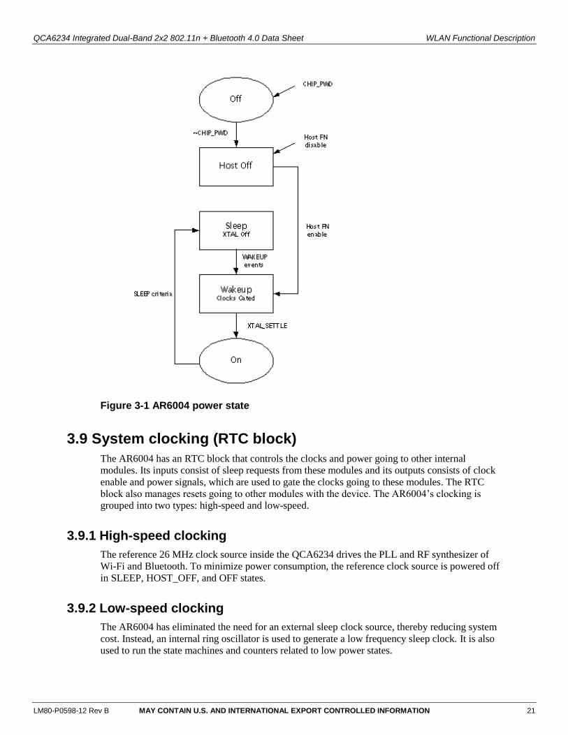
3.8.1 Hardware power states
AR6004 hardware has five top-level hardware power states managed by the RTC block. Table 3-
1 describes the input from the MAC, CPU, SDIO/MBOX, interrupt logic, and timers that affect
the power states.
3.8.2 Sleep state management
Sleep state minimizes power consumption while saving system states. In SLEEP state, all high
speed clocks are gated off and the external reference clock source is powered off. For the
AR6004 to enter SLEEP state, the MAC, MBOX, and CPU systems must not be active.
The system remains in sleep state until a WAKEUP event causes the system to enter WAKEUP
state; wait for the reference clock source to stabilize, and then ungate all enabled clock trees. The
CPU wakes up only when an interrupt arrives, which may have also generated the system
WAKEUP event.

QCA6234 Integrated Dual-Band 2x2 802.11n + Bluetooth 4.0 Data Sheet WLAN Functional Description
LM80-P0598-12 Rev B MAY CONTAIN U.S. AND INTERNATIONAL EXPORT CONTROLLED INFORMATION 20
Table 3-1 Power management states
State Description
OFF CHIP_PWD_L pin assertion immediately brings the chip to this state.
Sleep clock is disabled.
No state is preserved.
HOST_OFF WLAN is turned off. The Bluetooth clock is off, but should also be powered down through BT_PWD_L.
Only the host interface is powered on, the rest of the chip is power gated (off).
The host instructs the AR6004 to transition to WAKEUP by writing a register in the host
interface domain.
Embedded CPU and WLAN do not retain state (separate entry).
For USB/HSIC or hostless designs, this state can be bypassed by asserting FORCE_HOST_ON_L during CHIP_PWD_L de-assertion.
SLEEP Only the sleep clock is operating.
The crystal or oscillator is disabled.
Any wakeup events (MAC, host, LF-Timer, GPIO-interrupt) will force a transition from this state to the WAKEUP state.
All internal states are maintained.
WAKEUP The system transitions from sleep states to ON.
The high frequency clock is gated off as the crystal or oscillator is brought up and the PLL is enabled.
WAKEUP duration is programmable.
ON The high speed clock is operational and sent to each block enabled by the clock control register.
Lower level clock gating is implemented at the block level, including the CPU, which can be gated off using the WAIT instruction while the system is on. No CPU, host, and WLAN activities will transition to sleep states. WLAN must be initialized prior to Bluetooth initialization and use.
QCA6234 Integrated Dual-Band 2x2 802.11n + Bluetooth 4.0 Data Sheet WLAN Functional Description
LM80-P0598-12 Rev B MAY CONTAIN U.S. AND INTERNATIONAL EXPORT CONTROLLED INFORMATION 21
Figure 3-1 AR6004 power state
3.9 System clocking (RTC block)
The AR6004 has an RTC block that controls the clocks and power going to other internal
modules. Its inputs consist of sleep requests from these modules and its outputs consists of clock
enable and power signals, which are used to gate the clocks going to these modules. The RTC
block also manages resets going to other modules with the device. The AR6004’s clocking is
grouped into two types: high-speed and low-speed.
3.9.1 High-speed clocking
The reference 26 MHz clock source inside the QCA6234 drives the PLL and RF synthesizer of
Wi-Fi and Bluetooth. To minimize power consumption, the reference clock source is powered off
in SLEEP, HOST_OFF, and OFF states.
3.9.2 Low-speed clocking
The AR6004 has eliminated the need for an external sleep clock source, thereby reducing system
cost. Instead, an internal ring oscillator is used to generate a low frequency sleep clock. It is also
used to run the state machines and counters related to low power states.

QCA6234 Integrated Dual-Band 2x2 802.11n + Bluetooth 4.0 Data Sheet WLAN Functional Description
LM80-P0598-12 Rev B MAY CONTAIN U.S. AND INTERNATIONAL EXPORT CONTROLLED INFORMATION 22
The AR6004 has an internal calibration module that produces a 32.768 KHz output with minimal
variation. For this, it uses the reference clock source as the golden clock. As a result, the
calibration module adjusts for process and temperature variations in the ring oscillator when the
system is in ON state.
The AR6004 also supports using an external low frequency sleep clock source in applications
where one is already available.
3.9.3 Interface clock
The host interface clock represents another clock domain for the AR6004. This clock comes from
the SDIO and is completely independent from the other internal clocks. It drives the host interface
logic as well as certain registers, which can be accessed by the host in HOST_OFF and SLEEP
states.
3.10 MAC/BB/RF block
The AR6004 wireless MAC consists of five major blocks:
Host interface unit (HIU) for bridging to the AHB for bulk data accesses and APB for register
accesses
Ten queue control units (QCU) for transferring TX data
Ten DCF control units (DCU) for managing channel access
Protocol control unit (PCU) for interfacing to baseband
DMA receive unit (DRU) for transferring RX data
3.11 Baseband block
The AR6004 baseband module (BB) is the physical layer controller for the 802.11b/g/n air
interface. It is responsible for modulating data packets in the transmit direction, and detecting and
demodulating data packets in the receive direction. It has a direct control interface to the radio to
enable hardware to adjust analog gains and modes dynamically.
3.12 Design for test
The AR6004 has a built-in JTAG boundary scan of its pins. It also has features that enable testing
of digital blocks via ATPG scan, memories via MBIST, analog components, and the radio.

LM80-P0598-12 Rev B MAY CONTAIN U.S. AND INTERNATIONAL EXPORT CONTROLLED INFORMATION 23
4 Bluetooth Functional Description
The QCA6234 Bluetooth (BT) block is based on the QTI AR3002 and described in the following
sections.
4.1 HCI-UART interface
The UART interface is a standard high speed UART interface, being able to operate up to 4
Mbps, supporting Bluetooth HCI UART interface.
4.2 PCM interface
A PCM interface to an external mono-audio CODEC is supported. The BT block supports
CODECs: Winbond W681360, Wolfson WM8974, and Realtek ALC5620. The PCM supports
both 8 KHz/16 KHz frequencies.
The BT block can operate as the PCM interface master generating an output clock or configured
as a PCM interface slave. It supports 13-bit, 16-bit, 8-bit, or 14-bit µ-law, A-law, or linear mono-
sample formats at 8K, 16K, 32K, 48K, 64K, and 96K sample(s).
4.3 CPU and memory
The BT block uses a 32-bit RISC core with five-stage pipelining and 16-bit and 24-bit instruction
encoding. On startup, the BT block boots from the boot ROM. Software checks OTP first for
configuration information. It then gets configuration from the host and proceeds to execute from
on-chip ROM.
4.4 Standard WLAN coexistence
The QCA6234 supports internally the standard WLAN coexistence interface through the
WLAN_ACTIVE, BT_PRIORITY, and BT_ACTIVE pins.
4.5 QTI proprietary coexistence interface
The QTI proprietary interface enables increased information sharing between the Bluetooth and
WLAN blocks. The interface allows the same information exchange as the on-chip interface of a
single chip solution. Additional interface HW allows synchronizing the timing of the two devices.
The timing synchronization and additional information enables superior WLAN and Bluetooth
scheduling for increased throughput, longer range, better audio quality, and lower power
consumption.

QCA6234 Integrated Dual-Band 2x2 802.11n + Bluetooth 4.0 Data Sheet Bluetooth Functional Description
LM80-P0598-12 Rev B MAY CONTAIN U.S. AND INTERNATIONAL EXPORT CONTROLLED INFORMATION 24
4.6 Reference clock
The BT block is configured for 26 MHz reference clock frequency. The clock source is provided
to BT internally from the WLAN block on demand from BT_CLK_REQ. The WLAN block must
be initialized before BT clock sharing is enabled.
4.7 BT low energy
The QCA6234 supports low energy specification, which allows for connection to devices with
single mode LE function, for example, Watch, Sensor, and HID. The implementation is optimized
for coexistence with WLAN.
4.8 Reset
The pin BT_PWD_L resets and powers down the BT block.
Holding the BT_PWD_L pin at GND turns off the entire BT block and all state information is
lost.
All core supply voltages are internally gated off in this condition to minimize leakage.
The power-on-reset (POR) circuit detects a low-to-high transition on this pin and executes a reset
after BT_VDD has stabilized.
4.9 Radio
The BT radio shares the single antenna port with WLAN through an internal 3-way RF switch.
The QCA6234 implements WLAN/BT coexistence internally.
BT_VDDPA provides power to the BT PA and must be connected to the same supply voltage as
BT_VDD at 1.8 V.
4.10 GPIO
A single output pin BT_LED is provided to drive an indicator LED. This pin indicates Bluetooth
activity and status.
The BT_DISABLE pin is not used and should be connected to ground.

LM80-P0598-12 Rev B MAY CONTAIN U.S. AND INTERNATIONAL EXPORT CONTROLLED INFORMATION 25
5 Electrical Characteristics
5.1 Absolute maximum ratings
Table 5-1 summarizes the absolute maximum ratings and Table 5-2 lists the recommended
operating conditions for the QCA6234. Absolute maximum ratings are those values beyond
which damage to the device can occur.
Functional operation under these conditions, or at any other condition beyond those indicated in
the operational sections of this document, is not recommended.
NOTE: Maximum rating for signals follows the supply domain of the signals.
Table 5-1 Absolute maximum ratings
Symbol (Domain) Parameter Max Rating Unit
SDIO_IOVDD WLAN host interface I/O supply -0.3 to 4.0 V
IOVDD, BT_IOVDD WLAN and BT GPIO I/O power supply -0.3 to 4.0 V
VBAT_VDD33 External 3.3 V power supply -0.3 to 4.2 V
VDD33 External 3.3 V power supply -0.3 to 4.0 V
VDD33_REG External 3.3 V power supply -0.3 to 3.65 V
BT_VDD BT Power core supply 3.6 V
BT_VDDPA BT PA supply 3.6 V
TSTORE Storage Temperature -45 to +125 °C
ANT_2G Maximum RF input (reference to 50-Ω input) +10 dBm
ESD Electrostatic discharge tolerance
5G TX1 1000 V
All other pins 1500 V
5.2 Recommended operating conditions
Table 5-2 Recommended operating conditions
Symbol (Domain) Parameter Min Typ Max Unit
SDIO_IOVDD WLAN host interface I/O supply 1.71 1.8/3.3 3.46 V
IOVDD WLAN GPIO I/O power supply 1.71 1.8 3.46 V
BT_IOVDD BT GPIO I/O power supply 1.71 1.8/3.3 3.46 V
VBAT_VDD33 External 3.3 V power supply 3.14 3.30 3.46 V
VDD33 External 3.3 V power supply 3.14 3.30 3.46 V
VDD33_REG External 3.3 V power supply 3.14 3.30 3.46 V
BT_VDD BT core supply 1.71 1.8 1.98 V

QCA6234 Integrated Dual-Band 2x2 802.11n + Bluetooth 4.0 Data Sheet Electrical Characteristics
LM80-P0598-12 Rev B MAY CONTAIN U.S. AND INTERNATIONAL EXPORT CONTROLLED INFORMATION 26
Symbol (Domain) Parameter Min Typ Max Unit
BT_VDDPA BT PA supply 1.71 1.8 1.98 V
Tambient Ambient temperature -20 25 85 °C
5.3 DC electrical characteristics
Table 5-3 lists the general DC electrical characteristics over recommended operating conditions
(unless otherwise specified).
Table 5-3 General DC electrical characteristics (for 3.3 V I/O operation)
Symbol Parameter Conditions Min Typ Max Unit
VIH High Level Input Voltage 0.7 x VDD V
VIL Low Level Input Voltage 0.3 x VDD V
IIL Input Leakage Current
Without Pull-up or Pull-down
0 V < VIN < VDD
0 V < VOUT < VDD 0 -3 nA
With Pull-up 0 V < VIN < VDD
0 V < VOUT < VDD 16 48 A
With Pull-down 0 V < VIN < VDD
0 V < VOUT < VDD -14 -47 A
VOH High Level Output Voltage IOH = -4mA 0.9 x VDD V
IOH = -12mA 0.9 x VDD V
VOL Low Level Output Voltage IOH = 4mA 0.1 x VDD V
IOH = 12mA 0.1 x VDD V
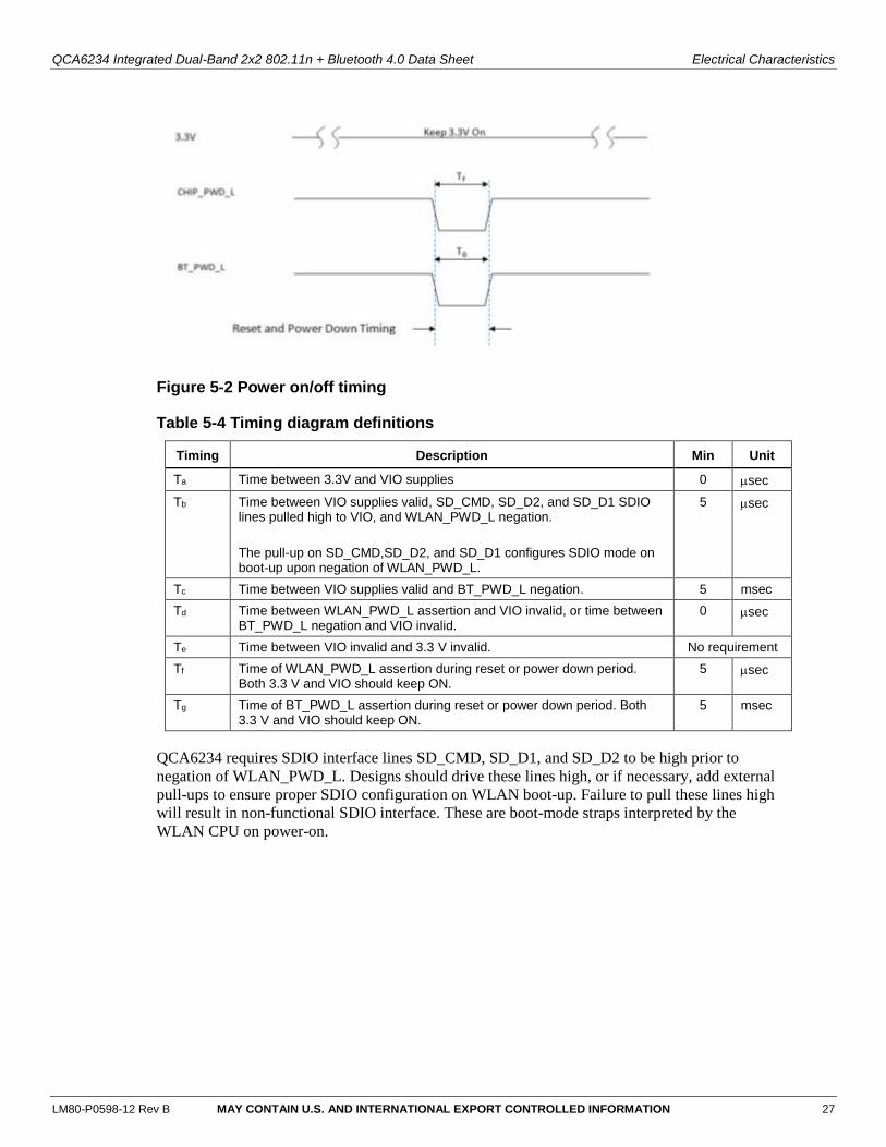
Figure 5-1 Power on/off timing
QCA6234 Integrated Dual-Band 2x2 802.11n + Bluetooth 4.0 Data Sheet Electrical Characteristics
LM80-P0598-12 Rev B MAY CONTAIN U.S. AND INTERNATIONAL EXPORT CONTROLLED INFORMATION 27
Figure 5-2 Power on/off timing
Table 5-4 Timing diagram definitions
Timing Description Min Unit
Ta Time between 3.3V and VIO supplies 0 sec
Tb Time between VIO supplies valid, SD_CMD, SD_D2, and SD_D1 SDIO lines pulled high to VIO, and WLAN_PWD_L negation.
The pull-up on SD_CMD,SD_D2, and SD_D1 configures SDIO mode on boot-up upon negation of WLAN_PWD_L.
5 sec
Tc Time between VIO supplies valid and BT_PWD_L negation. 5 msec
Td Time between WLAN_PWD_L assertion and VIO invalid, or time between BT_PWD_L negation and VIO invalid.
0 sec
Te Time between VIO invalid and 3.3 V invalid. No requirement
Tf Time of WLAN_PWD_L assertion during reset or power down period. Both 3.3 V and VIO should keep ON.
5 sec
Tg Time of BT_PWD_L assertion during reset or power down period. Both 3.3 V and VIO should keep ON.
5 msec
QCA6234 requires SDIO interface lines SD_CMD, SD_D1, and SD_D2 to be high prior to
negation of WLAN_PWD_L. Designs should drive these lines high, or if necessary, add external
pull-ups to ensure proper SDIO configuration on WLAN boot-up. Failure to pull these lines high
will result in non-functional SDIO interface. These are boot-mode straps interpreted by the
WLAN CPU on power-on.
QCA6234 Integrated Dual-Band 2x2 802.11n + Bluetooth 4.0 Data Sheet Electrical Characteristics
LM80-P0598-12 Rev B MAY CONTAIN U.S. AND INTERNATIONAL EXPORT CONTROLLED INFORMATION 28
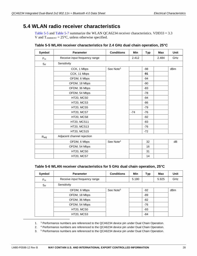
5.4 WLAN radio receiver characteristics
Table 5-5 and Table 5-7 summarize the WLAN QCA6234 receiver characteristics. VDD33 = 3.3
V and TAMBIENT = 25°C, unless otherwise specified.
Table 5-5 WLAN receiver characteristics for 2.4 GHz dual chain operation, 25°C
Symbol Parameter Conditions Min Typ Max Unit
Frx Receive input frequency range 2.412 2.484 GHz
Srf Sensitivity
CCK, 1 Mbps See Note3 -98 dBm
CCK, 11 Mbps -91
OFDM, 6 Mbps -94
OFDM, 18 Mbps -90
OFDM, 36 Mbps -83
OFDM, 54 Mbps -78
HT20, MCS0 -94
HT20, MCS3 -86
HT20, MCS5 -79
HT20, MCS7 -74 -76
HT20, MCS8 -92
HT20, MCS11 -83
HT20, MCS13 -76
HT20, MCS15 -72
Radj Adjacent channel rejection
OFDM, 6 Mbps See Note4 32 dB
OFDM, 54 Mbps 16
HT20, MCS0 31
HT20, MCS7 14
Table 5-6 WLAN receiver characteristics for 5 GHz dual chain operation, 25°C
Symbol Parameter Conditions Min Typ Max Unit
Frx Receive input frequency range 5.180 5.925 GHz
Srf Sensitivity
OFDM, 6 Mbps See Note5 -92 dBm
OFDM, 18 Mbps -89
OFDM, 36 Mbps -82
OFDM, 54 Mbps -76
HT20, MCS0 -93
HT20, MCS3 -84
1. 3 Performance numbers are referenced to the QCA6234 device pin under Dual Chain Operation.
2. 4 Performance numbers are referenced to the QCA6234 device pin under Dual Chain Operation.
3. 5 Performance numbers are referenced to the QCA6234 device pin under Dual Chain Operation.
QCA6234 Integrated Dual-Band 2x2 802.11n + Bluetooth 4.0 Data Sheet Electrical Characteristics
LM80-P0598-12 Rev B MAY CONTAIN U.S. AND INTERNATIONAL EXPORT CONTROLLED INFORMATION 29
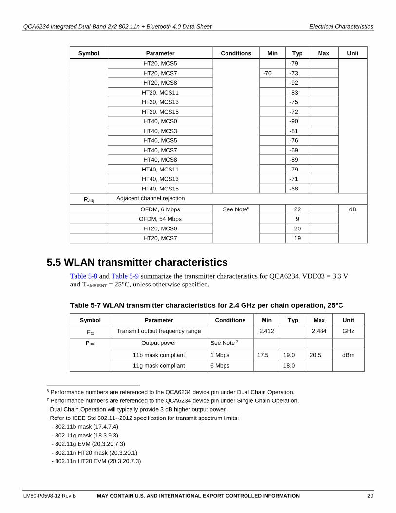
Symbol Parameter Conditions Min Typ Max Unit
HT20, MCS5 -79
HT20, MCS7 -70 -73
HT20, MCS8 -92
HT20, MCS11 -83
HT20, MCS13 -75
HT20, MCS15 -72
HT40, MCS0 -90
HT40, MCS3 -81
HT40, MCS5 -76
HT40, MCS7 -69
HT40, MCS8 -89
HT40, MCS11 -79
HT40, MCS13 -71
HT40, MCS15 -68
Radj Adjacent channel rejection
OFDM, 6 Mbps See Note6 22 dB
OFDM, 54 Mbps 9
HT20, MCS0 20
HT20, MCS7 19
5.5 WLAN transmitter characteristics
Table 5-8 and Table 5-9 summarize the transmitter characteristics for QCA6234. VDD33 = 3.3 V
and TAMBIENT = 25°C, unless otherwise specified.
Table 5-7 WLAN transmitter characteristics for 2.4 GHz per chain operation, 25°C
Symbol Parameter Conditions Min Typ Max Unit
Ftx Transmit output frequency range 2.412 2.484 GHz
Pout Output power See Note 7
11b mask compliant 1 Mbps 17.5 19.0 20.5 dBm
11g mask compliant 6 Mbps 18.0
6 Performance numbers are referenced to the QCA6234 device pin under Dual Chain Operation. 7 Performance numbers are referenced to the QCA6234 device pin under Single Chain Operation.
Dual Chain Operation will typically provide 3 dB higher output power.
Refer to IEEE Std 802.11--2012 specification for transmit spectrum limits:
- 802.11b mask (17.4.7.4)
- 802.11g mask (18.3.9.3)
- 802.11g EVM (20.3.20.7.3)
- 802.11n HT20 mask (20.3.20.1)
- 802.11n HT20 EVM (20.3.20.7.3)

QCA6234 Integrated Dual-Band 2x2 802.11n + Bluetooth 4.0 Data Sheet Electrical Characteristics
LM80-P0598-12 Rev B MAY CONTAIN U.S. AND INTERNATIONAL EXPORT CONTROLLED INFORMATION 30
Symbol Parameter Conditions Min Typ Max Unit
11g EVM compliant 54 Mbps 14.0 15.5 17.0
11n HT20 mask compliant MCS0 15.0 16.5 18.0
11n HT20 EVM compliant MCS7 12.5 14.0 15.5
11n HT20 EVM compliant MCS15 12.5
ATx Transmit power accuracy - - - +1.5 dB
Table 5-8 WLAN transmitter characteristics for 5 GHz per chain operation, 25°C
Symbol Parameter Conditions Min Typ Max Unit
Ftx Transmit output frequency range 5.180 5.925 GHz
Pout Output power See Note8
11a mask compliant 6 Mbps 17 dBm
11a EVM compliant 54 Mbps 11.5 13.5 15.5
11n HT20 mask compliant MCS0 15.5 17.5 19.5
11n HT20 EVM compliant MCS7 10.5 12.5 14.5
11n HT20 EVM compliant MCS15 10.5
11n HT40 mask compliant MCS0 14.5
11n HT40 EVM compliant MCS7 12.0
11n HT40 EVM compliant MCS15 10.5
ATx Transmit power accuracy - - - +2.0 dB
5.6 Typical WLAN power consumption performance
Table 5-9 QCA6234 typical WLAN current consumption in SDIO mode – low power states at 3.3 V operation, TAMBIENT = 25°C
Mode VDD33 (mA)
Single Chain
DVDD_SDIO
(mA)
VDD33 (mA)
Dual Chain
DVDD_SDI
O (mA)
Standby OFF 0.007 0 0.007 0
HOST_OFF 0.050 0.04 0.050 0.04
SLEEP 0.250 0.05 0.250 0.05
DTIM=1 2.28 0.10 2.75 0.10
8 Performance numbers are referenced to the QCA6234 device pin under Single Chain Operation. Dual Chain Operation will typically provide 3 dB higher output power. Refer to IEEE Std 802.11--2012 specification for transmit spectrum limits: - 802.11b mask (17.4.7.4) - 802.11g mask (18.3.9.3) - 802.11g EVM (20.3.20.7.3) - 802.11n HT20 mask (20.3.20.1) - 802.11n HT20 EVM (20.3.20.7.3)

QCA6234 Integrated Dual-Band 2x2 802.11n + Bluetooth 4.0 Data Sheet Electrical Characteristics
LM80-P0598-12 Rev B MAY CONTAIN U.S. AND INTERNATIONAL EXPORT CONTROLLED INFORMATION 31
Mode VDD33 (mA)
Single Chain
DVDD_SDIO
(mA)
VDD33 (mA)
Dual Chain
DVDD_SDI
O (mA)
IEEE PS, 2.4 GHz
DTIM=3 1.02 0.08 1.14 0.08
DTIM=10 0.52 0.06 0.56 0.06
IEEE PS, 5 GHz
DTIM=1 1.33 0.10 1.43 0.10
DTIM=3 0.64 0.08 0.65 0.08
DTIM=10 0.40 0.06 0.41 0.06
Table 5-10 QCA6234 typical WLAN current consumption in HSIC mode – low power states at 3.3 V operation, TAMBIENT = 25oC
Mode VDD33 (mA)
Single Chain
DVDD_SDIO
(mA)
VDD33 (mA)
Dual Chain
DVDD_SDI
O (mA)
Standby OFF 0.007 0 0.007 0
SLEEP 0.400 0.05 0.400 0.05
IEEE PS, 2.4 GHz
DTIM=1 3.41 0.10 3.82 0.10
DTIM=3 1.46 0.08 1.59 0.08
DTIM=10 0.77 0.06 0.81 0.06
IEEE PS, 5 GHz DTIM=1 1.68 0.10 1.78 0.10
DTIM=3 0.88 0.08 0.91 0.08
DTIM=10 0.60 0.06 0.61 0.06
Table 5-11 Typical WLAN current consumption [2.4 GHz operation] – continuous receive at 3.3 V operation, TAMBIENT = 25°C
Mode/Rate [Mbps] Typical Current Consumption
Single Chain (mA)9
Typical Current Consumption
Dual Chain (mA)10
RX, 1 Mbps 65 77
RX, 11 Mbps 66 77
RX, 54 Mbps 69 81
RX, HT20 MCS0 67 74
RX, HT20 MCS7 69 83
RX, HT20 MCS15 -- 88
9 With LPL enabled. 10 With LPL enabled.

QCA6234 Integrated Dual-Band 2x2 802.11n + Bluetooth 4.0 Data Sheet Electrical Characteristics
LM80-P0598-12 Rev B MAY CONTAIN U.S. AND INTERNATIONAL EXPORT CONTROLLED INFORMATION 32
Table 5-12 Typical WLAN current consumption [2.4 GHz operation] – continuous transmit at 3.3 V operation, TAMBIENT = 25°C
Mode/Rate
[Mbps]
Output Power
Per Chain
[dBm]11
Typical Current
Consumption Single Chain
(mA)
Typical Current Consumption
Dual Chain (mA)
TX, 1 Mbps 19.0 300 542
TX, 6 Mbps 18.0 276 491
TX, 54 Mbps 15.5 250 446
TX, HT20 MCS0 16.5 250 446
TX, HT20 MCS7 14.0 205 350
Table 5-13 Typical WLAN current consumption [5 GHz operation] – continuous receive at 3.3 V operation, TAMBIENT = 25°C
Mode/Rate [Mbps] Typical Current Consumption
Single Chain (mA)
Typical Current Consumption
Dual Chain (mA)
RX, 54 Mbps 75 82
RX, HT20 MCS0 79 87
RX, HT20 MCS7 81 89
RX, HT20 MCS15 -- 91
RX, HT40 MCS0 91 105
RX, HT40 MCS7 93 107
RX, HT40 MCS15 -- 115
Table 5-14 Typical WLAN current consumption [5 GHz operation] – continuous transmit at 3.3 V operation, TAMBIENT = 25°C
Mode/Rate
[Mbps]
Output Power
Per Chain
[dBm] 12
Typical Current
Consumption Single Chain
(mA)
Typical Current Consumption
Dual Chain (mA)
TX, 6 Mbps 17.0 342 640
TX, 54 Mbps 13.5 300 541
TX, HT20 MCS0 17.5 343 626
TX, HT20 MCS7 12.5 297 534
TX, HT40 MCS0 14.5 333 604
TX, HT40 MCS7 12.0 287 503
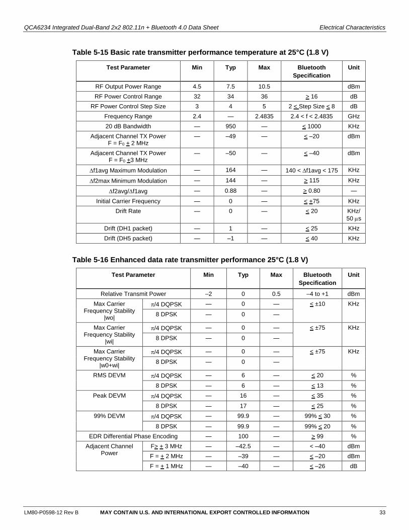
5.7 Bluetooth radio characteristics
Table 5-15 through Table 5-18 describe the basic rate transmitter performance, enhanced data
transmitter performance, basic rate receiver performance, enhanced rate receiver performance,
and current consumption conditions at 25°C.
11 RF power referenced at the SiP output. 12 RF power referenced at the SiP output.
QCA6234 Integrated Dual-Band 2x2 802.11n + Bluetooth 4.0 Data Sheet Electrical Characteristics
LM80-P0598-12 Rev B MAY CONTAIN U.S. AND INTERNATIONAL EXPORT CONTROLLED INFORMATION 33
Table 5-15 Basic rate transmitter performance temperature at 25°C (1.8 V)
Test Parameter Min Typ Max Bluetooth
Specification
Unit
RF Output Power Range 4.5 7.5 10.5 dBm
RF Power Control Range 32 34 36 > 16 dB
RF Power Control Step Size 3 4 5 2 < Step Size < 8 dB
Frequency Range 2.4 — 2.4835 2.4 < f < 2.4835 GHz
20 dB Bandwidth — 950 — < 1000 KHz
Adjacent Channel TX Power F = F0 + 2 MHz
— –49 — < –20 dBm
Adjacent Channel TX Power F = F0 +3 MHz
— –50 — < –40 dBm
f1avg Maximum Modulation — 164 — 140 < f1avg < 175 KHz
f2max Minimum Modulation — 144 — > 115 KHz
f2avg/f1avg — 0.88 — > 0.80 —
Initial Carrier Frequency — 0 — < +75 KHz
Drift Rate — 0 — < 20 KHz/
50 s
Drift (DH1 packet) — 1 — < 25 KHz
Drift (DH5 packet) — –1 — < 40 KHz
Table 5-16 Enhanced data rate transmitter performance 25°C (1.8 V)
Test Parameter Min Typ Max Bluetooth
Specification
Unit
Relative Transmit Power –2 0 0.5 –4 to +1 dBm
Max Carrier Frequency Stability
|wo|
/4 DQPSK — 0 — < ±10 KHz
8 DPSK — 0 —
Max Carrier Frequency Stability
|wi|
/4 DQPSK — 0 — < ±75 KHz
8 DPSK — 0 —
Max Carrier Frequency Stability
|w0+wi|
/4 DQPSK — 0 — < ±75 KHz
8 DPSK — 0 —
RMS DEVM /4 DQPSK — 6 — < 20 %
8 DPSK — 6 — < 13 %
Peak DEVM /4 DQPSK — 16 — < 35 %
8 DPSK — 17 — < 25 %
99% DEVM /4 DQPSK — 99.9 — 99% < 30 %
8 DPSK — 99.9 — 99% < 20 %
EDR Differential Phase Encoding — 100 — > 99 %
Adjacent Channel Power
F> + 3 MHz — –42.5 — < –40 dBm
F = + 2 MHz — –39 — < –20 dBm
F = + 1 MHz — –40 — < –26 dB

QCA6234 Integrated Dual-Band 2x2 802.11n + Bluetooth 4.0 Data Sheet Electrical Characteristics
LM80-P0598-12 Rev B MAY CONTAIN U.S. AND INTERNATIONAL EXPORT CONTROLLED INFORMATION 34
Table 5-17 Basic rate receiver performance at 1.8 V
Test Parameter Min Typ Max Bluetooth
Specification
Unit
Sensitivity BER < 0.1% — –91 — < –70 dBm
Maximum Input BER < 0.1% –20 — — > –20 dBm
Carrier-to-Interferer Ratio (C/I)
Co-Channel — — 11 11
Adjacent Channel (+ 1 MHz)
— — 0 0 dB
Second Adjacent Channel (± 2 MHz)
— — –30 –30 dB
Third Adjacent Channel
(± 3 MHz)
— — –40 –40 dB
Maximum Level of Intermodulation Interferers — — –39 < –39 dBm
Table 5-18 Enhanced data rate receiver performance 1.8 V
Test Parameter Min Typ Max Bluetooth
Specification
Unit
Sensitivity (BER < 0.01%)
/4 DQPSK — -92 — < –70 dBm
8 DPSK — -87 — < –70 dBm
Maximum Input (BER < 0.1%)
/4 DQPSK -20 — — > –20 dBm
8 DPSK -20 — — > –20 dBm
Co-Channel C/I (BER < 0.1%)
/4 DQPSK — — 13 < ±13 dB
8 DPSK — — 20 < ±20 dB
Adjacent Channel C/I (BER< 0.1%)
/4 DQPSK — — 0 < 0 dB
8 DPSK — — 5 < 5 dB
Second Adjacent Channel C/I
(BER < 0.1%)
/4 DQPSK — — –30 < –30 dB
8 DPSK — — –25 < –25 dB
Third Adjacent Channel C/I (BER < 0.1%)
/4 DQPSK — — –40 < –40 dB
8 DPSK — — –33 < –33 dB
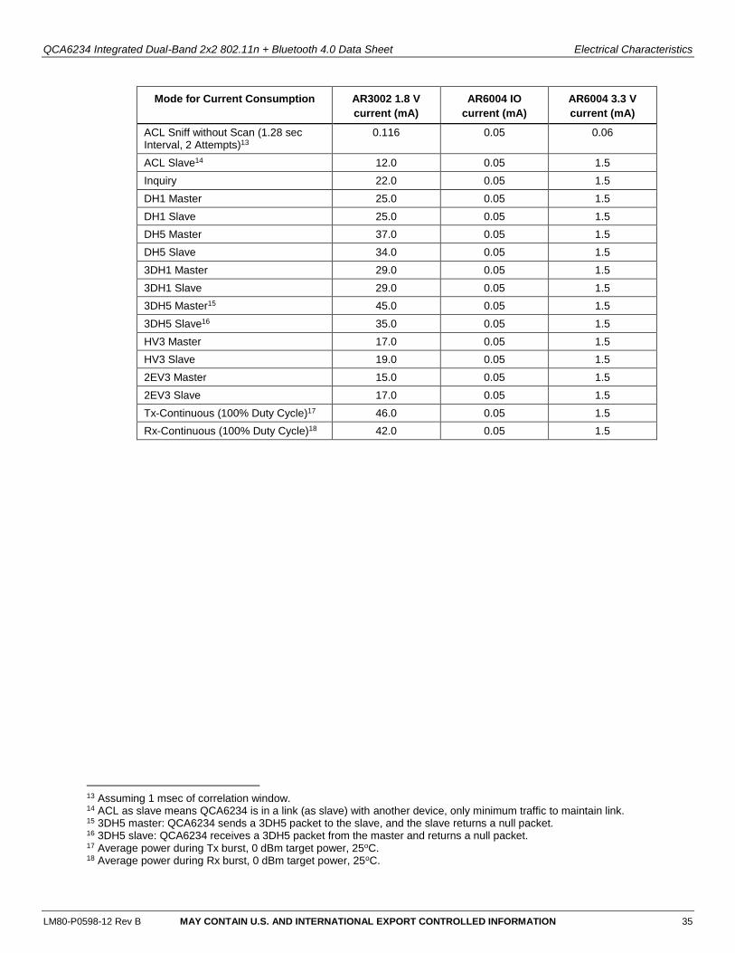
5.8 Typical Bluetooth power consumption performance
Table 5-19 Typical Bluetooth power consumption with UART interface, AR6004 in HOST_OFF mode, BT_VDD=1.8 V, TX=0 dBm, 25°C
Mode for Current Consumption AR3002 1.8 V
current (mA)
AR6004 IO
current (mA)
AR6004 3.3 V
current (mA)
Idle Mode 0.093 0.05 0
Inquiry Scan (1.28 sec) 0.485 0.05 0.015
Page Scan (1.28 sec) 0.485 0.05 0.015
Page and Inq Scan (1.28 sec) 0.877 0.05 0.03
QCA6234 Integrated Dual-Band 2x2 802.11n + Bluetooth 4.0 Data Sheet Electrical Characteristics
LM80-P0598-12 Rev B MAY CONTAIN U.S. AND INTERNATIONAL EXPORT CONTROLLED INFORMATION 35
Mode for Current Consumption AR3002 1.8 V
current (mA)
AR6004 IO
current (mA)
AR6004 3.3 V
current (mA)
ACL Sniff without Scan (1.28 sec Interval, 2 Attempts)13
0.116 0.05 0.06
ACL Slave14 12.0 0.05 1.5
Inquiry 22.0 0.05 1.5
DH1 Master 25.0 0.05 1.5
DH1 Slave 25.0 0.05 1.5
DH5 Master 37.0 0.05 1.5
DH5 Slave 34.0 0.05 1.5
3DH1 Master 29.0 0.05 1.5
3DH1 Slave 29.0 0.05 1.5
3DH5 Master15 45.0 0.05 1.5
3DH5 Slave16 35.0 0.05 1.5
HV3 Master 17.0 0.05 1.5
HV3 Slave 19.0 0.05 1.5
2EV3 Master 15.0 0.05 1.5
2EV3 Slave 17.0 0.05 1.5
Tx-Continuous (100% Duty Cycle)17 46.0 0.05 1.5
Rx-Continuous (100% Duty Cycle)18 42.0 0.05 1.5
13 Assuming 1 msec of correlation window. 14 ACL as slave means QCA6234 is in a link (as slave) with another device, only minimum traffic to maintain link. 15 3DH5 master: QCA6234 sends a 3DH5 packet to the slave, and the slave returns a null packet. 16 3DH5 slave: QCA6234 receives a 3DH5 packet from the master and returns a null packet. 17 Average power during Tx burst, 0 dBm target power, 25oC. 18 Average power during Rx burst, 0 dBm target power, 25oC.

LM80-P0598-12 Rev B MAY CONTAIN U.S. AND INTERNATIONAL EXPORT CONTROLLED INFORMATION 36
6 Pin Assignments and Descriptions
This chapter describes the pin assignment of the QCA6234.
The following nomenclature is used for signal description described in this chapter.
NC No Connection should be made to this pin
_L Suffix at the end of the signal name indicating active low signal
A_I/O Analog signal
I Digital input signal
PU Weak internal pull-up, input can be left floating (not connected)
PD Weak internal pull-down, input can be left floating (not connected)
I/O A digital bidirectional signal
O A digital output signal
P A power or ground pin
N/A Not applicable
X Indeterminate, floating inputs must be externally driven high or low
Figure 6-1 QCA6234 LGA pin-out view
DOT 1 2 3 4 5 6 7 8 9 10 11 12 13
ASWREG_
OUTVDD33_PMU WLAN_TDO WLAN_TMS AVDD12 DVDD12 GND IOVDD BT_IOVDD PAREG_BASE VBAT_VDD33 VDD33 VDD33
BSWREG_
OUTVDD33_PMU WLAN_TDI WLAN_TCK AVDD12 DVDD12 GND VDD12_USB VDD33_USB PAREG_FB VDD33 VDD33
CSDIO_
IOVDD
USB_D+/
HSIC_DATAGND GND
DWLAN_
PWD_L
USB_D-/
HSIC_STROBEGND 2G_ANT1
E SD_CMD SD_D3 GND GND GND GND GND GND GND
F SD_D2 SD_D1 GND GND GND GND GND GND 5G_ANT1
G SD_D0 SD_CLK GND GND GND GND GND GND GND
HCLK_REQ_OUT/
WCN_
PRIORITY
CLK_REQ_IN GND GND GND GND GND TM0
JDEBUG_
UART_TXD
WAKE_ON_
WLANGND GND GND GND GND TM1 BT_VDD
K BT_FREQWLAN_
ACTIVEGND BT_VDDPA
L BT_ACTIVEBT_
PRIORITY
BT_WKUP_
HOSTBT_DISABLE
MGPIO10/
LTE_FRAME_
SYNC
AR6004_
GPIO38GND GND GND GND GND PCM_SYNC PCM_OUT
BT_UART_
CTSGND
BT_UART_
RXDBT_WKUP_BT
N LTE_ACTIVE GND 2G_ANT0 GND 5G_ANT0 GND PCM_BCLK PCM_INBT_UART_
RTSBT_LED
BT_UART_
TXDBT_PWD_L

QCA6234 Integrated Dual-Band 2x2 802.11n + Bluetooth 4.0 Data Sheet Pin Assignments and Descriptions
LM80-P0598-12 Rev B MAY CONTAIN U.S. AND INTERNATIONAL EXPORT CONTROLLED INFORMATION 37
Table 6-1 QCA6234 pin definitions
Grid Signal Name Description Type Reset
State
I/O Pad Supply
Domain
Power Supplies
C1 DVDD _SDIO WLAN Host IO (SDIO) power supply input; 1.8 V
P N/A N/A
A8 IOVDD WLAN VIO power supply input; 1.8 V
P N/A N/A
A11 VBAT_VDD33 WLAN VBAT supply input. Connect to 3.3 V.
P N/A N/A
A10 PAREG_BASE PAREG gate control output. O N/A N/A
B11 PAREG_FB Signal should be connected to 3.3 V output of external pass transistor when using PAREG.
P N/A N/A
A12,A13,
B12,B13
VDD33 WLAN 3.3 V power supply input to WLAN PA.
P N/A N/A
A1,B1 SWREG_OUT On-chip 1.2V switching
regulator inductor.
No connect for USB version
(6234XU)
P N/A N/A
A6,B6 DVDD12 WLAN internal digital 1.2 V input fed from switching regulator filter.
P N/A N/A
A5,B5 AVDD12 WLAN internal analog 1.2 V input fed from switching regulator filter.
P N/A N/A
A2,B2 VDD33_REG WLAN 3.3 V power supply input to on-chip 1.2 V switching regulator.
P N/A N/A
J13 BT_VDD BT core power supply input.
1.8 V. Must be same as BT_IOVDD.
P N/A N/A
K13 BT_VDDPA Power supply for BT PA.
Must be same as BT_IOVDD.
P N/A N/A
A9 BT_IOVDD BT VIO power supply input. Must be same voltage as IOVDD due to internal interconnection between WLAN and BT.
P N/A N/A
B8 VDD12_USB Serial interface 1.2 V input fed from switching regulator filter.
P N/A N/A
B9 VDD33_USB Serial interface 3.3 V input. Connect to 3.3 V.
P N/A N/A
See pin-out GND Ground P N/A N/A
WLAN Host Interface
G2 SD_CLK SDIO Clock signal I Hi-Z SDIO_IOVDD
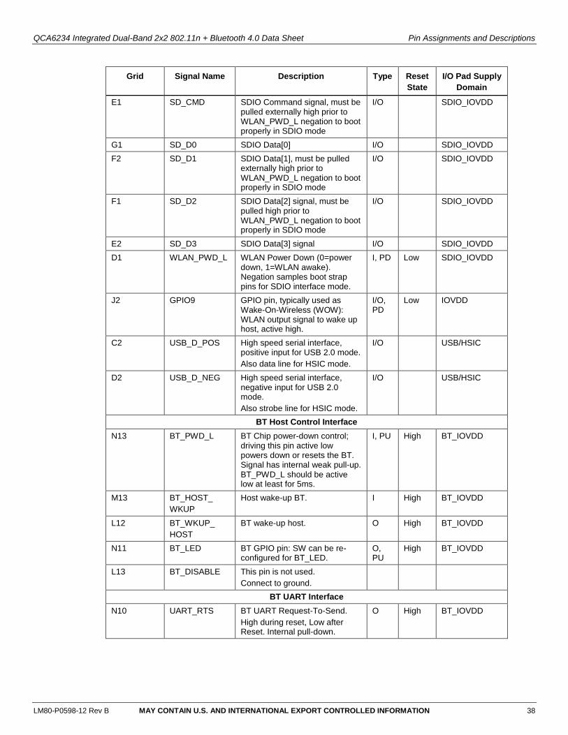
QCA6234 Integrated Dual-Band 2x2 802.11n + Bluetooth 4.0 Data Sheet Pin Assignments and Descriptions
LM80-P0598-12 Rev B MAY CONTAIN U.S. AND INTERNATIONAL EXPORT CONTROLLED INFORMATION 38
Grid Signal Name Description Type Reset
State
I/O Pad Supply
Domain
E1 SD_CMD SDIO Command signal, must be pulled externally high prior to WLAN_PWD_L negation to boot properly in SDIO mode
I/O SDIO_IOVDD
G1 SD_D0 SDIO Data[0] I/O SDIO_IOVDD
F2 SD_D1 SDIO Data[1], must be pulled externally high prior to WLAN_PWD_L negation to boot properly in SDIO mode
I/O SDIO_IOVDD
F1 SD_D2 SDIO Data[2] signal, must be pulled high prior to WLAN_PWD_L negation to boot properly in SDIO mode
I/O SDIO_IOVDD
E2 SD_D3 SDIO Data[3] signal I/O SDIO_IOVDD
D1 WLAN_PWD_L WLAN Power Down (0=power down, 1=WLAN awake). Negation samples boot strap pins for SDIO interface mode.
I, PD Low SDIO_IOVDD
J2 GPIO9 GPIO pin, typically used as Wake-On-Wireless (WOW): WLAN output signal to wake up host, active high.
I/O, PD
Low IOVDD
C2 USB_D_POS High speed serial interface, positive input for USB 2.0 mode.
Also data line for HSIC mode.
I/O USB/HSIC
D2 USB_D_NEG High speed serial interface, negative input for USB 2.0 mode.
Also strobe line for HSIC mode.
I/O USB/HSIC
BT Host Control Interface
N13 BT_PWD_L BT Chip power-down control; driving this pin active low powers down or resets the BT. Signal has internal weak pull-up. BT_PWD_L should be active low at least for 5ms.
I, PU High BT_IOVDD
M13 BT_HOST_
WKUP
Host wake-up BT. I High BT_IOVDD
L12 BT_WKUP_
HOST
BT wake-up host. O High BT_IOVDD
N11 BT_LED BT GPIO pin: SW can be re-configured for BT_LED.
O, PU
High BT_IOVDD
L13 BT_DISABLE This pin is not used.
Connect to ground.
BT UART Interface
N10 UART_RTS BT UART Request-To-Send.
High during reset, Low after Reset. Internal pull-down.
O High BT_IOVDD
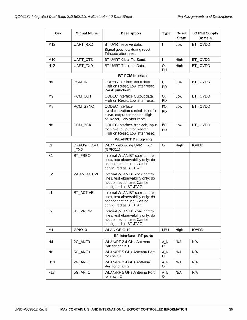
QCA6234 Integrated Dual-Band 2x2 802.11n + Bluetooth 4.0 Data Sheet Pin Assignments and Descriptions
LM80-P0598-12 Rev B MAY CONTAIN U.S. AND INTERNATIONAL EXPORT CONTROLLED INFORMATION 39
Grid Signal Name Description Type Reset
State
I/O Pad Supply
Domain
M12 UART_RXD BT UART receive data.
Signal goes low during reset, Tri-state after reset.
I Low BT_IOVDD
M10 UART_CTS BT UART Clear-To-Send. I High BT_IOVDD
N12 UART_TXD BT UART Transmit Data O, PU
High BT_IOVDD
BT PCM Interface
N9 PCM_IN CODEC interface Input data. High on Reset, Low after reset. Weak pull-down.
I,
PD
Low BT_IOVDD
M9 PCM_OUT CODEC interface Output data. High on Reset, Low after reset.
O, PD
Low BT_IOVDD
M8 PCM_SYNC CODEC interface synchronization control, input for slave, output for master. High on Reset, Low after reset.
I/O,
PD
Low BT_IOVDD
N8 PCM_BCK CODEC interface bit clock, input for slave, output for master. High on Reset, Low after reset.
I/O,
PD
Low BT_IOVDD
WLAN/BT Debugging
J1 DEBUG_UART_TXD
WLAN debugging UART TXD (GPIO11)
O High IOVDD
K1 BT_FREQ Internal WLAN/BT coex control lines, test observability only; do not connect or use. Can be configured as BT JTAG.
K2 WLAN_ACTIVE Internal WLAN/BT coex control lines, test observability only; do not connect or use. Can be configured as BT JTAG.
L1 BT_ACTIVE Internal WLAN/BT coex control lines, test observability only; do not connect or use. Can be configured as BT JTAG.
L2 BT_PRIOR Internal WLAN/BT coex control lines, test observability only; do not connect or use. Can be configured as BT JTAG.
M1 GPIO10 WLAN GPIO 10 I,PU High IOVDD
RF Interface - RF ports
N4 2G_ANT0 WLAN/RF 2.4 GHz Antenna Port for chain 1
A_I/O
N/A N/A
N6 5G_ANT0 WLAN/RF 5 GHz Antenna Port for chain 1
A_I/O
N/A N/A
D13 2G_ANT1 WLAN/RF 2.4 GHz Antenna Port for chain 2
A_I/O
N/A N/A
F13 5G_ANT1 WLAN/RF 5 GHz Antenna Port for chain 2
A_I/O
N/A N/A

QCA6234 Integrated Dual-Band 2x2 802.11n + Bluetooth 4.0 Data Sheet Pin Assignments and Descriptions
LM80-P0598-12 Rev B MAY CONTAIN U.S. AND INTERNATIONAL EXPORT CONTROLLED INFORMATION 40
Grid Signal Name Description Type Reset
State
I/O Pad Supply
Domain
Clock - BT Clock
H2 GPIO7 Internal BT Clock Request signal. It has internal connection from BT to WLAN GPIO7. Do not use this pin, leave as No connect. Useful only for test.
I/O Low IOVDD
H1 GPIO37 LTE co-existence signal WCN_PRIORITY.
O, PU
High IOVDD
BT Loopback
H12 BT_TM0 Bluetooth test mode.
Do not connect.
J12 BT_TM1 Bluetooth test mode.
Do not connect.
WLAN Boundary Scan
A4 WLAN_TMS No Connect (NC)
B4 WLAN_TCK No Connect (NC)
B3 WLAN_TDI No Connect (NC)
A3 WLAN_TDO No Connect (NC)
LTE Co-existence
N2 GPIO36 LTE co-existence signal LTE_ACTIVE
N1 GPIO35 LTE co-existence signal LTE_FRAME_SYNC
M2 GPIO38 Reserved

LM80-P0598-12 Rev B MAY CONTAIN U.S. AND INTERNATIONAL EXPORT CONTROLLED INFORMATION 41
7 Package Dimensions
Figure 7-1 shows the top and side views of QCA6234 (with height).
Figure 7-1 QCA6234 package top and side views
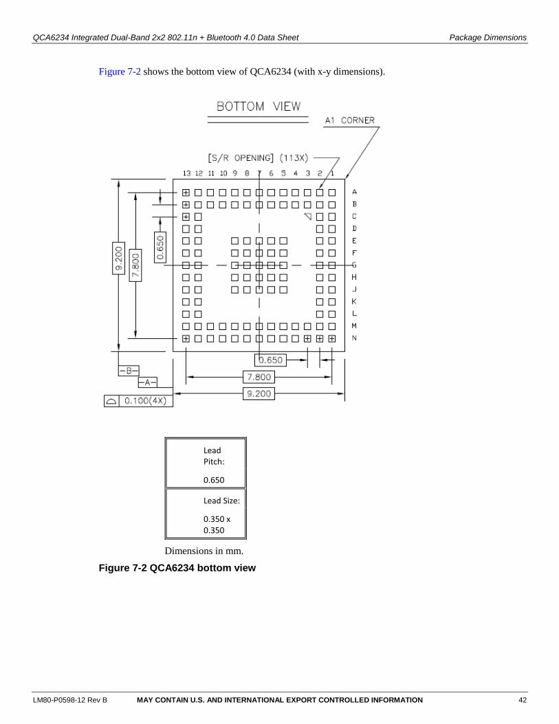
QCA6234 Integrated Dual-Band 2x2 802.11n + Bluetooth 4.0 Data Sheet Package Dimensions
LM80-P0598-12 Rev B MAY CONTAIN U.S. AND INTERNATIONAL EXPORT CONTROLLED INFORMATION 42
Figure 7-2 shows the bottom view of QCA6234 (with x-y dimensions).
Lead Pitch:
0.650
Lead Size:
0.350 x 0.350
Dimensions in mm.
Figure 7-2 QCA6234 bottom view

LM80-P0598-12 Rev B MAY CONTAIN U.S. AND INTERNATIONAL EXPORT CONTROLLED INFORMATION 43
8 Ordering Information
This product can be ordered as:
SDIO interface version:
QCA6234X-AM2D
QCA6234X-AM2D-R (Tape and Reel, Qty = 2Ku)
QCA6234XW-AM2D*
QCA6234XW-AM2D-R* (Tape and Reel, Qty = 2Ku)
QCA6234X2-AM2D*
QCA6234X2-AM2D-R* (Tape and Reel, Qty = 2Ku)
HSIC interface version:
QCA6234XH-AM2D
QCA6234XH-AM2D-R (Tape and Reel, Qty = 2Ku)
USB interface version
QCA6234XU–AM2D
QCA6234XU–AM2D-R (Tape and Reel, Qty = 2Ku)
* Contact your local QTI representative for availability.

LM80-P0598-12 Rev B MAY CONTAIN U.S. AND INTERNATIONAL EXPORT CONTROLLED INFORMATION 44
9 Part Reliability Summary
Table 9-1 QCA6234 device reliability test results
Tests, Standards, and Conditions Sample Size Result
ESD – Human-body model (HBM) rating
JESD22-A114
Target: 2000 V.
(Total samples from one wafer lot)
1x3 +1.5KV PASS all pins,
Except 5G Tx1 pass +1KV
ESD – Charge-device model (CDM) rating JESD22-C101
Target: 500 V
(Total samples from one wafer lot)
1x3 +500V PASS
Table 9-2 QCA6234 package reliability test results
Tests, Standards, and Conditions Sample Size Result
Preconditioning:
J-STD-020, JESD22-A113
MSL 1, reflow temperature: 260C+0/-5°C
(Total samples from three different assembly lots)
3x154 PASS
Temperature cycle: (after Preconditioning)
JESD22-A104
-55°C to +125°C; 1000 cycles
2 cycles per hour
(Total samples from three different assembly lots)
3x77 PASS
Unbiased Highly accelerated stress test (uHAST): (after Preconditioning)
JESD22-A118, JESD22-A113
cond. A, 130C, 96 hours
(Total samples from three different assembly lots)
3x77 PASS
High-Temperature Storage Life:
JESD22-A103
Temperature 150°C, 1000 hours duration
(Total samples from three different assembly lots)
3x77 PASS

LM80-P0598-12 Rev B MAY CONTAIN U.S. AND INTERNATIONAL EXPORT CONTROLLED INFORMATION 45
10 Carriage, Storage & Handling Information
This chapter describes career tape system, tape and reel, and storage requirements for the
QCA6234. See Table 10-1.
10.1 10.1 Carrier Tape System
Table 10-1 Reel and Protective Band Attributes
Units per Reel Tape Width Tape Pitch Reel Diameter Hub Diameter
2000 24 mm 12 mm 330 mm 178 mm
10.1.1 Tape and Reel Information
The single-feed carrier for the QCA6234 device is illustrated in Figure 10-1 which shows the tape
orientation on reel. Figure 10-2 shows the part orientation on tape.
The carrier tape and reel features comply to the EIA-481 standard.
Figure 10-1 Tape Orientation on Reel

QCA6234 Integrated Dual-Band 2x2 802.11n + Bluetooth® 4.0 Data Sheet Carriage, Storage & Handling Information
LM80-P0598-12 Rev B MAY CONTAIN U.S. AND INTERNATIONAL EXPORT CONTROLLED INFORMATION 46
Figure 10-2 Device Orientation in Tape: Left/Q1
10.2 Storage
10.2.1 Bag storage conditions
The packages described in this document must be stored in a nitrogen-purged, sealed moisture
barrier antistatic bag. The Qualcomm-calculated shelf life in a sealed moisture bag is 60 months
at < 40°C and < 90% relative humidity (RH). Qualcomm recommends the following shipping and
storage conditions for the CSP reel inside the sealed bag:
Relative humidity between 15% and 70%
Temperature – Room temperature lower than 30°C
Atmosphere – A nitrogen dry cabinet is highly preferred
Devices should not be baked in tapes and reels at the temperatures described in this section, or at
any other temperatures.
10.2.2 Out of Bag Duration
After unpacking, the package must be soldered to the PCB within the factory floor life according
to the MSL rating when factory conditions are < 30°C and < 60% RH, as specified in the
IPC/JEDEC-STD-033 standard.
10.3 Handling
In addition to the storage guidelines described above, the following handling guidelines should be
followed.
To eliminate damage to the silicon die due to improper handling, the following recommendations
should be followed:
Do not use tweezers, as that may cause damage to the silicon die. Qualcomm recommends
using a vacuum tip to handle the device.

QCA6234 Integrated Dual-Band 2x2 802.11n + Bluetooth® 4.0 Data Sheet Carriage, Storage & Handling Information
LM80-P0598-12 Rev B MAY CONTAIN U.S. AND INTERNATIONAL EXPORT CONTROLLED INFORMATION 47
Carefully select a pickup tool to avoid any damage during the SMT process.
Do not make contact with the device when reworking or tuning components that are in close
proximity to the device.
10.3.1 Baking
It is not necessary to bake the QCA6234 if the conditions specified in Section 10.2 have not been
exceeded.
It is necessary to bake the QCA6234 if any condition specified in Section 10.2 has been
exceeded. The baking conditions are specified on the moisture-sensitive caution label attached to
each bag.
CAUTION: If baking is required, the devices must be transferred into trays that can be baked to at
least 125°C. Devices should not be baked in tape and reel carriers at any temperature.
10.3.2 Electrostatic Discharge
Electrostatic discharge (ESD) occurs naturally in laboratory and factory environments. An
established high-voltage potential is always at risk of discharging to a lower potential. If this
discharge path is through a semiconductor device, destructive damage may result.
ESD countermeasures and handling methods must be developed and used to control the factory
environment at each manufacturing site.
QTI products must be handled according to the ESD Association standard: ANSI/ESD S20.20-
1999, Protection of Electrical and Electronic Parts, Assemblies, and Equipment.

LM80-P0598-12 Rev B MAY CONTAIN U.S. AND INTERNATIONAL EXPORT CONTROLLED INFORMATION 48
Exhibit 1
PLEASE READ THIS LICENSE AGREEMENT (“AGREEMENT”) CAREFULLY. THIS AGREEMENT IS A BINDING LEGAL AGREEMENT ENTERED INTO BY AND BETWEEN YOU (OR IF YOU ARE ENTERING INTO THIS AGREEMENT ON BEHALF OF AN ENTITY, THEN THE ENTITY THAT YOU REPRESENT) AND QUALCOMM TECHNOLOGIES, INC. (“QTI” “WE” “OUR” OR “US”). THIS IS THE AGREEMENT THAT APPLIES TO YOUR USE OF THE DESIGNATED AND/OR ATTACHED DOCUMENTATION AND ANY UPDATES OR IMPROVEMENTS THEREOF (COLLECTIVELY, “MATERIALS”). BY USING OR COMPLETING THE INSTALLATION OF THE MATERIALS, YOU ARE ACCEPTING THIS AGREEMENT AND YOU AGREE TO BE BOUND BY ITS TERMS AND CONDITIONS. IF YOU DO NOT AGREE TO THESE TERMS, QTI IS UNWILLING TO AND DOES NOT LICENSE THE MATERIALS TO YOU. IF YOU DO NOT AGREE TO THESE TERMS YOU MUST DISCONTINUE AND YOU MAY NOT USE THE MATERIALS OR RETAIN ANY COPIES OF THE MATERIALS. ANY USE OR POSSESSION OF THE MATERIALS BY YOU IS SUBJECT TO THE TERMS AND CONDITIONS SET FORTH IN THIS AGREEMENT.
1.1 License. Subject to the terms and conditions of this Agreement, including, without limitation, the restrictions, conditions, limitations and exclusions set forth in this Agreement, Qualcomm Technologies, Inc. (“QTI”) hereby grants to you a nonexclusive, limited license under QTI’s copyrights to use the attached Materials; and to reproduce and redistribute a reasonable number of copies of the Materials. You may not use Qualcomm Technologies or its affiliates or subsidiaries name, logo or trademarks; and copyright, trademark, patent and any other notices that appear on the Materials may not be removed or obscured. QTI shall be free to use suggestions, feedback or other information received from You, without obligation of any kind to You. QTI may immediately terminate this Agreement upon your breach. Upon termination of this Agreement, Sections 1.2-4 shall survive.
1.2 Indemnification. You agree to indemnify and hold harmless QTI and its officers, directors, employees and successors and assigns against any and all third party claims, demands, causes of action, losses, liabilities, damages, costs and expenses, incurred by QTI (including but not limited to costs of defense, investigation and reasonable attorney’s fees) arising out of, resulting from or related to: (i) any breach of this Agreement by You; and (ii) your acts, omissions, products and services. If requested by QTI, You agree to defend QTI in connection with any third party claims, demands, or causes of action resulting from, arising out of or in connection with any of the foregoing.
1.3 Ownership. QTI (or its licensors) shall retain title and all ownership rights in and to the Materials and all copies thereof, and nothing herein shall be deemed to grant any right to You under any of QTI's or its affiliates’ patents. You shall not subject the Materials to any third party license terms (e.g., open source license terms). You shall not use the Materials for the purpose of identifying or providing evidence to support any potential patent infringement claim against QTI, its affiliates, or any of QTI’s or QTI’s affiliates’ suppliers and/or direct or indirect customers. QTI hereby reserves all rights not expressly granted herein.
1.4 WARRANTY DISCLAIMER. YOU EXPRESSLY ACKNOWLEDGE AND AGREE THAT THE USE OF THE MATERIALS IS AT YOUR SOLE RISK. THE MATERIALS AND TECHNICAL SUPPORT, IF ANY, ARE PROVIDED "AS IS" AND WITHOUT WARRANTY OF ANY KIND, WHETHER EXPRESS OR IMPLIED. QTI ITS LICENSORS AND AFFILIATES MAKE NO WARRANTIES, EXPRESS OR IMPLIED, WITH RESPECT TO THE MATERIALS OR ANY OTHER INFORMATION OR DOCUMENTATION PROVIDED UNDER THIS AGREEMENT, INCLUDING BUT NOT LIMITED TO ANY WARRANTY OF MERCHANTABILITY OR FITNESS FOR A PARTICULAR PURPOSE OR AGAINST INFRINGEMENT, OR ANY EXPRESS OR IMPLIED WARRANTY ARISING OUT OF TRADE USAGE OR OUT OF A COURSE OF DEALING OR COURSE OF PERFORMANCE. NOTHING CONTAINED IN THIS AGREEMENT SHALL BE CONSTRUED AS (I) A WARRANTY OR REPRESENTATION BY QTI, ITS LICENSORS OR AFFILIATES AS TO THE VALIDITY OR SCOPE OF ANY PATENT, COPYRIGHT OR OTHER INTELLECTUAL PROPERTY RIGHT OR (II) A WARRANTY OR REPRESENTATION BY QTI THAT ANY MANUFACTURE OR USE WILL BE FREE FROM INFRINGEMENT OF PATENTS, COPYRIGHTS OR OTHER INTELLECTUAL PROPERTY RIGHTS OF OTHERS, AND IT SHALL BE THE SOLE RESPONSIBILITY OF YOU TO MAKE SUCH DETERMINATION AS IS NECESSARY WITH RESPECT TO THE ACQUISITION OF LICENSES UNDER PATENTS AND OTHER INTELLECTUAL PROPERTY OF THIRD PARTIES.
1.5 LIMITATION OF LIABILITY. IN NO EVENT SHALL QTI, QTI’S AFFILIATES OR ITS LICENSORS BE LIABLE TO YOU FOR ANY INCIDENTAL, CONSEQUENTIAL OR SPECIAL DAMAGES, INCLUDING BUT NOT LIMITED TO ANY LOST PROFITS, LOST SAVINGS, OR OTHER INCIDENTAL DAMAGES, ARISING OUT OF THE USE OR INABILITY TO USE, OR THE DELIVERY OR FAILURE TO DELIVER, ANY OF THE MATERIALS, OR ANY BREACH OF ANY OBLIGATION UNDER THIS AGREEMENT, EVEN IF QTI HAS BEEN ADVISED OF THE POSSIBILITY OF SUCH DAMAGES. THE FOREGOING LIMITATION OF LIABILITY SHALL REMAIN IN FULL FORCE AND EFFECT REGARDLESS OF WHETHER YOUR REMEDIES HEREUNDER ARE DETERMINED TO HAVE FAILED OF THEIR ESSENTIAL PURPOSE. THE ENTIRE LIABILITY OF QTI, QTI’s AFFILIATES AND ITS LICENSORS, AND THE SOLE AND EXCLUSIVE REMEDY OF YOU, FOR ANY CLAIM OR CAUSE OF ACTION ARISING HEREUNDER (WHETHER IN CONTRACT, TORT, OR OTHERWISE) SHALL NOT EXCEED US$10.
2. COMPLIANCE WITH LAWS; APPLICABLE LAW. You agree to comply with all applicable local, international and national laws and regulations and with U.S. Export Administration Regulations, as they apply to the subject matter of this Agreement. This Agreement is governed by the laws of the State of California, excluding California’s choice of law rules.
3. CONTRACTING PARTIES. If the Materials are downloaded on any computer owned by a corporation or other legal entity, then this Agreement is formed by and between QTI and such entity. The individual accepting the terms of this Agreement represents and warrants to QTI that they have the authority to bind such entity to the terms and conditions of this Agreement.
4. MISCELLANEOUS PROVISIONS. This Agreement, together with all exhibits attached hereto, which are incorporated herein by this reference, constitutes the entire agreement between QTI and You and supersedes all prior negotiations, representations and agreements between the parties with respect to the subject matter hereof. No addition or modification of this Agreement shall be effective unless made in writing and signed by the respective representatives of QTI and You. The restrictions, limitations, exclusions and conditions set forth in this Agreement shall apply even if QTI or any of its affiliates becomes aware of or fails to act in a manner to address any violation or failure to comply therewith. You hereby acknowledge and agree that the restrictions, limitations, conditions and exclusions imposed in this Agreement on the rights granted in this Agreement are not a derogation of the benefits of such rights. You further acknowledges that, in the absence of such restrictions, limitations, conditions and exclusions, QTI would not have entered into this Agreement with You. Each party shall be responsible for and shall bear its own expenses in connection with this Agreement. If any of the provisions of this Agreement are determined to be invalid, illegal, or otherwise unenforceable, the remaining provisions shall remain in full force and effect. This Agreement is entered into solely in the English language, and if for any reason any other language version is prepared by any party, it shall be solely for convenience and the English version shall govern and control all aspects. If You are located in the province of Quebec, Canada, the following applies: The Parties hereby confirm they have requested this Agreement and all related documents be prepared in English.


