PXIe-5160 Calibration Procedure - National Instruments · PXIe-5160 and test instrumentation are at...
38
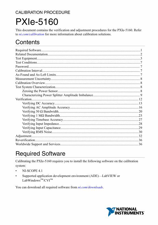
CALIBRATION PROCEDURE PXIe-5160 This document contains the verification and adjustment procedures for the PXIe-5160. Refer to ni.com/calibration for more information about calibration solutions. Contents Required Software.....................................................................................................................1 Related Documentation............................................................................................................. 2 Test Equipment..........................................................................................................................3 Test Conditions..........................................................................................................................7 Password................................................................................................................................... 7 Calibration Interval................................................................................................................... 7 As-Found and As-Left Limits................................................................................................... 7 Measurement Uncertainty......................................................................................................... 8 Calibration Overview................................................................................................................ 8 Test System Characterization.................................................................................................... 8 Zeroing the Power Sensor................................................................................................. 8 Characterizing Power Splitter Amplitude Imbalance....................................................... 9 Verification.............................................................................................................................. 12 Verifying DC Accuracy................................................................................................... 13 Verifying AC Amplitude Accuracy.................................................................................16 Verifying 50 Ω Bandwidth.............................................................................................. 20 Verifying 1 MΩ Bandwidth.............................................................................................23 Verifying Timebase Accuracy......................................................................................... 27 Verifying Input Impedance..............................................................................................28 Verifying Input Capacitance............................................................................................29 Verifying RMS Noise...................................................................................................... 30 Adjustment.............................................................................................................................. 32 Reverification.......................................................................................................................... 36 Worldwide Support and Services............................................................................................ 36 Required Software Calibrating the PXIe-5160 requires you to install the following software on the calibration system: • NI-SCOPE 4.1 • Supported application development environment (ADE)—LabVIEW or LabWindows ™ /CVI ™ You can download all required software from ni.com/downloads.
Transcript of PXIe-5160 Calibration Procedure - National Instruments · PXIe-5160 and test instrumentation are at...
CALIBRATION PROCEDURE
PXIe-5160This document contains the verification and adjustment procedures for the PXIe-5160. Referto ni.com/calibration for more information about calibration solutions.
ContentsRequired Software.....................................................................................................................1Related Documentation.............................................................................................................2Test Equipment..........................................................................................................................3Test Conditions..........................................................................................................................7Password................................................................................................................................... 7Calibration Interval................................................................................................................... 7As-Found and As-Left Limits................................................................................................... 7Measurement Uncertainty......................................................................................................... 8Calibration Overview................................................................................................................8Test System Characterization....................................................................................................8
Zeroing the Power Sensor................................................................................................. 8Characterizing Power Splitter Amplitude Imbalance....................................................... 9
Verification..............................................................................................................................12Verifying DC Accuracy...................................................................................................13Verifying AC Amplitude Accuracy.................................................................................16Verifying 50 Ω Bandwidth.............................................................................................. 20Verifying 1 MΩ Bandwidth.............................................................................................23Verifying Timebase Accuracy.........................................................................................27Verifying Input Impedance..............................................................................................28Verifying Input Capacitance............................................................................................29Verifying RMS Noise......................................................................................................30
Adjustment.............................................................................................................................. 32Reverification..........................................................................................................................36Worldwide Support and Services............................................................................................ 36
Required SoftwareCalibrating the PXIe-5160 requires you to install the following software on the calibrationsystem:• NI-SCOPE 4.1• Supported application development environment (ADE)—LabVIEW or
LabWindows™/CVI™
You can download all required software from ni.com/downloads.
Related DocumentationFor additional information, refer to the following documents as you perform the calibrationprocedure:• NI PXIe-5160/5162 Getting Started Guide• NI High-Speed Digitizers Help• NI PXIe-5160 Specifications
Visit ni.com/manuals for the latest versions of these documents.
2 | ni.com | PXIe-5160 Calibration Procedure
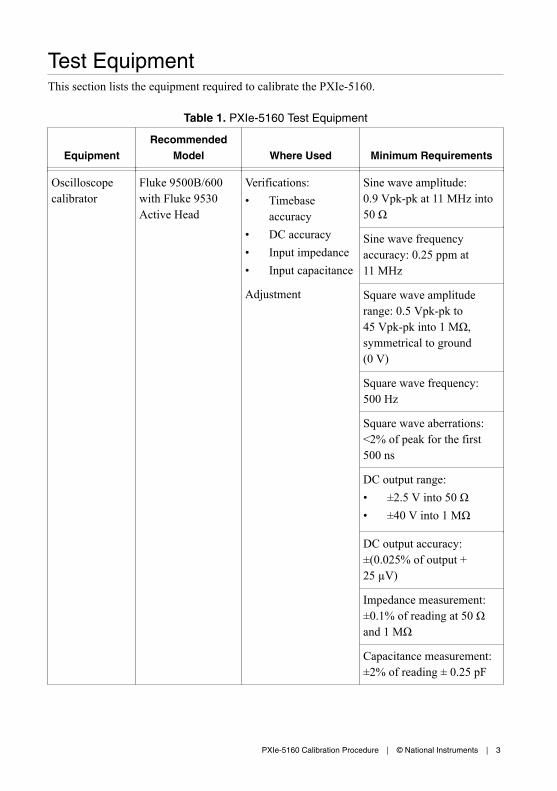
Test EquipmentThis section lists the equipment required to calibrate the PXIe-5160.
Table 1. PXIe-5160 Test Equipment
EquipmentRecommended
Model Where Used Minimum Requirements
Oscilloscopecalibrator
Fluke 9500B/600with Fluke 9530Active Head
Verifications:• Timebase
accuracy• DC accuracy• Input impedance• Input capacitance
Adjustment
Sine wave amplitude:0.9 Vpk-pk at 11 MHz into50 Ω
Sine wave frequencyaccuracy: 0.25 ppm at11 MHz
Square wave amplituderange: 0.5 Vpk-pk to45 Vpk-pk into 1 MΩ,symmetrical to ground(0 V)
Square wave frequency:500 Hz
Square wave aberrations:<2% of peak for the first500 ns
DC output range:• ±2.5 V into 50 Ω• ±40 V into 1 MΩ
DC output accuracy:±(0.025% of output +25 µV)
Impedance measurement:±0.1% of reading at 50 Ωand 1 MΩ
Capacitance measurement:±2% of reading ± 0.25 pF
PXIe-5160 Calibration Procedure | © National Instruments | 3
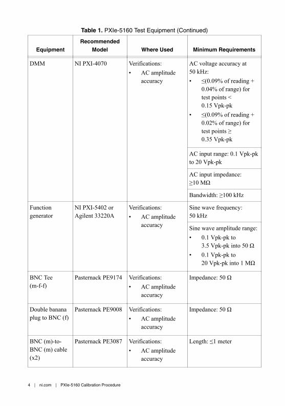
Table 1. PXIe-5160 Test Equipment (Continued)
EquipmentRecommended
Model Where Used Minimum Requirements
DMM NI PXI-4070 Verifications:• AC amplitude
accuracy
AC voltage accuracy at50 kHz:• ≤(0.09% of reading +
0.04% of range) fortest points <0.15 Vpk-pk
• ≤(0.09% of reading +0.02% of range) fortest points ≥0.35 Vpk-pk
AC input range: 0.1 Vpk-pkto 20 Vpk-pk
AC input impedance:≥10 MΩ
Bandwidth: ≥100 kHz
Functiongenerator
NI PXI-5402 orAgilent 33220A
Verifications:• AC amplitude
accuracy
Sine wave frequency:50 kHz
Sine wave amplitude range:• 0.1 Vpk-pk to
3.5 Vpk-pk into 50 Ω• 0.1 Vpk-pk to
20 Vpk-pk into 1 MΩ
BNC Tee(m-f-f)
Pasternack PE9174 Verifications:• AC amplitude
accuracy
Impedance: 50 Ω
Double bananaplug to BNC (f)
Pasternack PE9008 Verifications:• AC amplitude
accuracy
Impedance: 50 Ω
BNC (m)-to-BNC (m) cable(x2)
Pasternack PE3087 Verifications:• AC amplitude
accuracy
Length: ≤1 meter
4 | ni.com | PXIe-5160 Calibration Procedure

Table 1. PXIe-5160 Test Equipment (Continued)
EquipmentRecommended
Model Where Used Minimum Requirements
Power sensor Rohde & SchwarzNRP-Z91
Test systemcharacterization
Verifications:• Bandwidth
Range: -26 dBm to 10 dBm
Frequency range: 50 kHz to475.1 MHz
Absolute power accuracy:• <0.048 dB at 50 kHz• <0.063 dB at 475 MHz
Relative power accuracy:• <0.022 dB at 50 kHz• <0.031 dB at
475.1 MHz
VSWR: <1.11
Signal generator Rhode & SchwarzSMA100A
Test systemcharacterization
Verifications:• Bandwidth
Frequency range: 50 kHz to501 MHz
Amplitude range: -20 dBmto 16 dBm
Harmonics: <-30 dBc
Power splitter Aeroflex/Weinschel1593
Test systemcharacterization
Verifications:• Bandwidth
Frequency range: 50 kHz to501 MHz
VSWR: <1.1
Amplitude tracking:<0.5 dB
50 Ω BNCterminator (f)
FairviewMicrowave ST3B-F
Test systemcharacterization
Frequency range: DC to501 MHz
VSWR: <1.1
Impedance: 50 Ω
PXIe-5160 Calibration Procedure | © National Instruments | 5

Table 1. PXIe-5160 Test Equipment (Continued)
EquipmentRecommended
Model Where Used Minimum Requirements
50 Ω BNCterminator (m)
FairviewMicrowave ST2B
Verifications:• RMS noise
Frequency range: DC to501 MHz
VSWR: <1.15
Impedance: 50 Ω
SMA (m)-to-SMA (m) cable
— Test systemcharacterization
Verifications:• Bandwidth
Frequency range: DC to501 MHz
VSWR: <1.1
Length: ≤1 meter
SMA (f)-to-N(m) adapter
FairviewMicrowaveSM4226
Test systemcharacterization
Verifications:• Bandwidth
Frequency range: DC to501 MHz
VSWR: <1.05
Impedance: 50 Ω
BNC (f)-to-N(f) adapter
FairviewMicrowaveSM3526
Test systemcharacterization
Verifications:• Bandwidth
Frequency range: DC to501 MHz
VSWR: <1.1
Impedance: 50 Ω
SMA (m)-to-BNC (m)adapter (x2)
FairviewMicrowaveSM4716
Test systemcharacterization
Verifications:• Bandwidth
Frequency range: DC to501 MHz
VSWR: <1.1
Impedance: 50 Ω
BNC feed-throughterminator
FairviewMicrowave ST0150
Test systemcharacterization
Verifications:• Bandwidth
Frequency range: DC to301 MHz
VSWR:• <1.1 at 100 MHz• <1.25 at 301 MHz
Impedance: 50 Ω
6 | ni.com | PXIe-5160 Calibration Procedure
Test ConditionsThe following setup and environmental conditions are required to ensure the PXIe-5160 meetspublished specifications:• Keep cabling as short as possible. Long cables act as antennas, picking up extra noise that
can affect measurements.• Verify that all connections to the PXIe-5160, including front panel connections and
screws, are secure.• Use shielded copper wire for all cable connections to the device. Use twisted-pair wire to
eliminate noise and thermal offsets.• Maintain an ambient temperature of 23 °C ± 3 °C. The device temperature will be greater
than the ambient temperature.• Keep relative humidity between 10% and 90%, noncondensing.• Allow a warm-up time of at least 15 minutes after the chassis is powered on and
NI-SCOPE is loaded and recognizes the PXIe-5160. The warm-up time ensures that thePXIe-5160 and test instrumentation are at a stable operating temperature.
• Ensure that the PXI chassis fan speed is set to HIGH, that the fan filters (if present) areclean, and that the empty slots contain slot blockers and filler panels. For moreinformation about cooling, refer to the Maintain Forced-Air Cooling Note to Usersdocument available at ni.com/manuals.
• Plug the chassis and the instrument standard into the same power strip to avoid groundloops.
PasswordThe default password for password-protected operations is NI.
Calibration IntervalRecommended calibration interval 2 years
As-Found and As-Left LimitsThe as-found limits are the published specifications for the PXIe-5160. NI uses these limits todetermine whether the PXIe-5160 meets the specifications when it is received for calibration.Use the as-found limits during initial verification.
The as-left calibration limits are equal to the published NI specifications for the PXIe-5160,less guard bands for measurement uncertainty, temperature drift, and drift over time. NI usesthese limits to reduce the probability that the instrument will be outside the publishedspecification limits at the end of the calibration cycle. Use the as-left limits when performingverification after adjustment.
PXIe-5160 Calibration Procedure | © National Instruments | 7
Measurement UncertaintyMeasurement uncertainty was calculated in accordance with the method described in ISOGUM (Guide to the Expression of Uncertainty in Measurement), for a confidence level of95%. The expressed uncertainty is based on the recommended measurement methodology,standards, metrology best practices and environmental conditions of the National Instrumentslaboratory. It should be considered as a guideline for the level of measurement uncertainty thatcan be achieved using the recommended method. It is not a replacement for the useruncertainty analysis that takes into consideration the conditions and practices of the individualuser.
Calibration OverviewInstall the device and configure it in NI Measurement & Automation Explorer (MAX) beforecalibrating.
Calibration includes the following steps:1. Self-calibration—Adjust the self-calibration constants of the device.2. Test system characterization—Characterize the amplitude imbalance of the output ports
on your power splitter. The results of this step are used as a correction in the bandwidthverification procedure.
3. Verification—Verify the existing operation of the device. This step confirms whether thedevice is operating within the published specification prior to adjustment.
4. Adjustment—Perform an external adjustment of the calibration constants of the device.The adjustment procedure automatically stores the calibration date and temperature onthe EEPROM to allow traceability.
5. Re-verification—Repeat the Verification procedure to ensure that the device is operatingwithin the published specifications after adjustment.
Test System CharacterizationThe following procedures characterize the test equipment used during verification.
Caution The connectors on the device under test (DUT) and test equipment arefragile. Perform the steps in these procedures with great care to prevent damagingany DUTs or test equipment.
Zeroing the Power Sensor1. Ensure that the power sensor is not connected to any signals.2. Zero the power sensor using the built-in function, according to the power sensor
documentation.
8 | ni.com | PXIe-5160 Calibration Procedure

Characterizing Power Splitter Amplitude ImbalanceThis procedure characterizes the amplitude imbalance of the two output ports of the powersplitter over a range of frequencies.
The results of the characterization are later used as a correction in the Verifying 50 ΩBandwidth procedure and the Verifying 1 MΩ Bandwidth procedure.
Table 2. Power Splitter Characterization
Config
Test Point
Frequency (MHz) Amplitude (dBm)
1 0.05 -0.5
2 250.1 -0.5
3 300.1 -0.5
4 475.1 -0.5
1. Connect the BNC (f)-to-N (f) adapter to the power sensor. Refer to this assembly as thepower sensor.
2. Zero the power sensor as described in the Zeroing the Power Sensor section.3. Connect the RF OUT connector of the signal generator to the input port of the power
splitter using an SMA (f)-to-N (m) adapter and an SMA (m)-to-SMA (m) cable.4. Connect an SMA (m)-to-BNC (m) adapter to one of the power splitter output ports. Refer
to this assembly as splitter output 1.5. Connect the 50 Ω BNC terminator (f) to splitter output 1.6. Connect the other SMA (m)-to-BNC (m) adapter to the other output port of the power
splitter. Refer to this assembly as splitter output 2.7. Connect the power sensor to splitter output 2.
The following figure illustrates the hardware setup.
PXIe-5160 Calibration Procedure | © National Instruments | 9
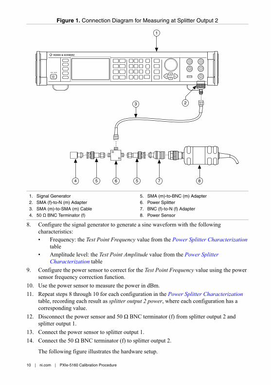
Figure 1. Connection Diagram for Measuring at Splitter Output 2
1
64 5
3
7 8
2
5
1. Signal Generator2. SMA (f)-to-N (m) Adapter3. SMA (m)-to-SMA (m) Cable4. 50 Ω BNC Terminator (f)
5. SMA (m)-to-BNC (m) Adapter6. Power Splitter7. BNC (f)-to-N (f) Adapter8. Power Sensor
8. Configure the signal generator to generate a sine waveform with the followingcharacteristics:• Frequency: the Test Point Frequency value from the Power Splitter Characterization
table• Amplitude level: the Test Point Amplitude value from the Power Splitter
Characterization table9. Configure the power sensor to correct for the Test Point Frequency value using the power
sensor frequency correction function.10. Use the power sensor to measure the power in dBm.11. Repeat steps 8 through 10 for each configuration in the Power Splitter Characterization
table, recording each result as splitter output 2 power, where each configuration has acorresponding value.
12. Disconnect the power sensor and 50 Ω BNC terminator (f) from splitter output 2 andsplitter output 1.
13. Connect the power sensor to splitter output 1.14. Connect the 50 Ω BNC terminator (f) to splitter output 2.
The following figure illustrates the hardware setup.
10 | ni.com | PXIe-5160 Calibration Procedure
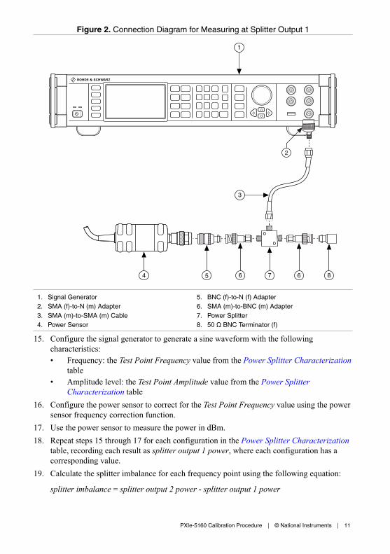
Figure 2. Connection Diagram for Measuring at Splitter Output 1
1
3
867654
2
1. Signal Generator2. SMA (f)-to-N (m) Adapter3. SMA (m)-to-SMA (m) Cable4. Power Sensor
5. BNC (f)-to-N (f) Adapter6. SMA (m)-to-BNC (m) Adapter7. Power Splitter8. 50 Ω BNC Terminator (f)
15. Configure the signal generator to generate a sine waveform with the followingcharacteristics:• Frequency: the Test Point Frequency value from the Power Splitter Characterization
table• Amplitude level: the Test Point Amplitude value from the Power Splitter
Characterization table16. Configure the power sensor to correct for the Test Point Frequency value using the power
sensor frequency correction function.17. Use the power sensor to measure the power in dBm.18. Repeat steps 15 through 17 for each configuration in the Power Splitter Characterization
table, recording each result as splitter output 1 power, where each configuration has acorresponding value.
19. Calculate the splitter imbalance for each frequency point using the following equation:
splitter imbalance = splitter output 2 power - splitter output 1 power
PXIe-5160 Calibration Procedure | © National Instruments | 11
20. Disconnect the 50 Ω BNC terminator (f) from splitter output 2. Refer to the remainingassembly as the power sensor assembly. The power sensor assembly will be used in the Verifying 50 Ω Bandwidth procedure and the Verifying 1 MΩ Bandwidth procedure.
VerificationThis section provides instructions for verifying the device specifications.
Verification of the PXIe-5160 is complete only after you have successfully completed all testsin this section using the As-Found Limits.
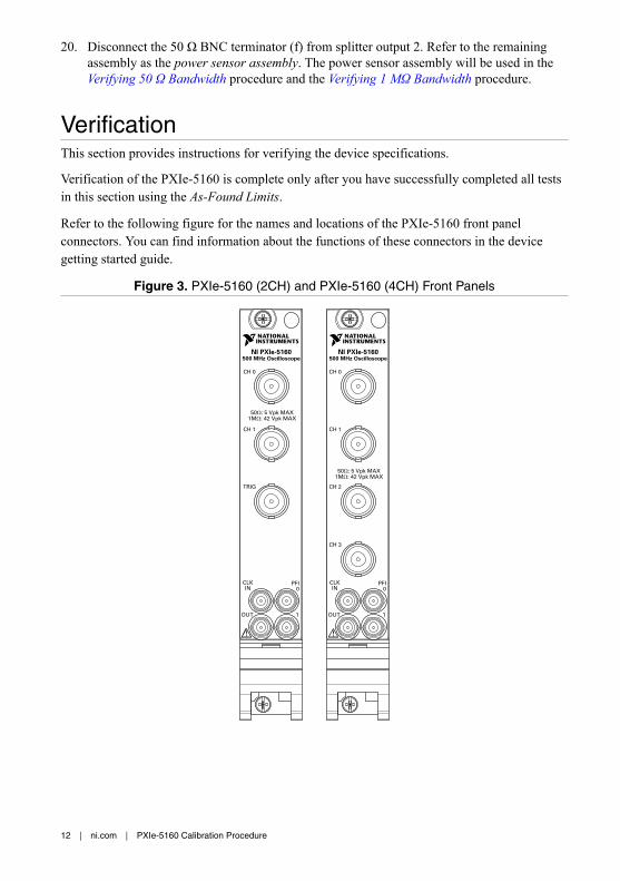
Refer to the following figure for the names and locations of the PXIe-5160 front panelconnectors. You can find information about the functions of these connectors in the devicegetting started guide.
Figure 3. PXIe-5160 (2CH) and PXIe-5160 (4CH) Front Panels
CH 0
50Ω: 5 Vpk MAX1MΩ: 42 Vpk MAX
CH 1
TRIG
CLKIN
PFI0
1OUT
NI PXIe-5160500 MHz Oscilloscope
CH 0
50Ω: 5 Vpk MAX1MΩ: 42 Vpk MAX
CH 1
CH 2
CLKIN
PFI0
1OUT
NI PXIe-5160500 MHz Oscilloscope
CH 3
12 | ni.com | PXIe-5160 Calibration Procedure

Verifying DC AccuracyThis procedure verifies the DC accuracy of the PXIe-5160 by comparing the voltage measuredby the device to the value sourced by the voltage standard.
Refer to the following table as you complete the following steps.
Table 3. DC Accuracy Verification
Config
InputImpedance
(Ω)
VerticalRange
(Vpk-pk)
VerticalOffset
(V)
TestPoints
(V)
As-FoundLimits(mV)
As-LeftLimits(mV)
MeasurementUncertainty
(mV)1
1 50 0.2 V 0 0.090 ±3.6 ±2.11 ±0.05
2 50 0.2 V 0 -0.090 ±3.6 ±2.11 ±0.05
3 50 0.2 V 0.5 0.590 ±10.6 ±4.16 ±0.15
4 50 0.2 V -0.5 -0.590 ±10.6 ±4.16 ±0.15
5 50 0.5 V 0 0.225 ±8.1 ±4.39 ±0.09
6 50 0.5 V 0 -0.225 ±8.1 ±4.39 ±0.09
7 50 0.5 V 0.5 0.725 ±15.1 ±6.44 ±0.18
8 50 0.5 V -0.5 -0.725 ±15.1 ±6.44 ±0.18
9 50 1 V 0 0.450 ±15.6 ±8.57 ±0.18
10 50 1 V 0 -0.450 ±15.6 ±8.57 ±0.18
11 50 1 V 0.5 0.950 ±22.6 ±10.62 ±0.26
12 50 1 V -0.5 -0.950 ±22.6 ±10.62 ±0.26
13 50 2 V 0 0.900 ±30.6 ±15.20 ±0.43
14 50 2 V 0 -0.900 ±30.6 ±15.20 ±0.43
15 50 2 V 1.5 2.400 ±51.6 ±20.90 ±0.48
16 50 2 V -1.5 -2.400 ±51.6 ±20.90 ±0.48
17 50 5 V 0 2.250 ±75.6 ±40.35 ±0.46
1 Measurement uncertainty based on Fluke 9500B with Fluke 9530 test head specifications thatapply at Tcal ± 5 °C, where Factory Tcal = 23 °C. Uncertainty of the 9500B includes long-termstability of 1 year (5 years for frequency), temperature coefficient, linearity, load, and lineregulation and traceability of factory and National Calibration Standard.
PXIe-5160 Calibration Procedure | © National Instruments | 13
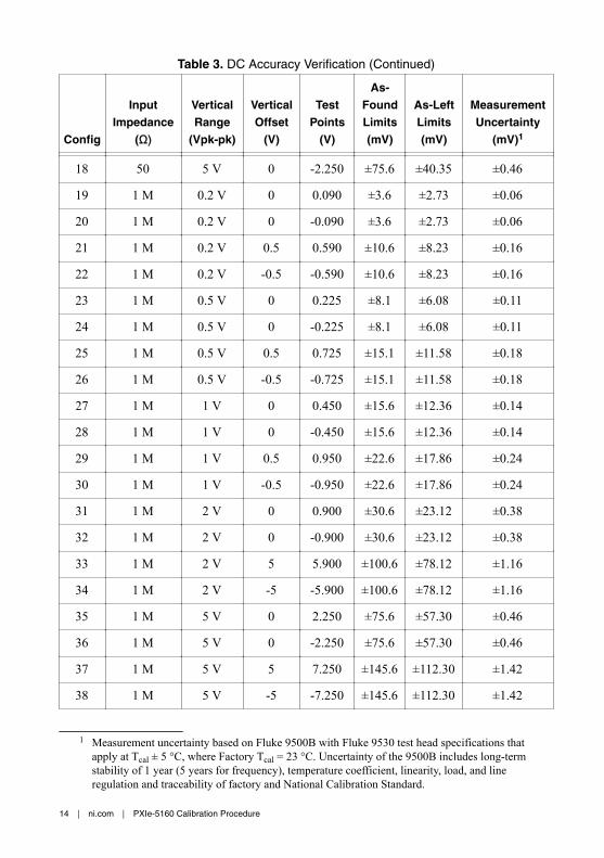
Table 3. DC Accuracy Verification (Continued)
Config
InputImpedance
(Ω)
VerticalRange
(Vpk-pk)
VerticalOffset
(V)
TestPoints
(V)
As-FoundLimits(mV)
As-LeftLimits(mV)
MeasurementUncertainty
(mV)1
18 50 5 V 0 -2.250 ±75.6 ±40.35 ±0.46
19 1 M 0.2 V 0 0.090 ±3.6 ±2.73 ±0.06
20 1 M 0.2 V 0 -0.090 ±3.6 ±2.73 ±0.06
21 1 M 0.2 V 0.5 0.590 ±10.6 ±8.23 ±0.16
22 1 M 0.2 V -0.5 -0.590 ±10.6 ±8.23 ±0.16
23 1 M 0.5 V 0 0.225 ±8.1 ±6.08 ±0.11
24 1 M 0.5 V 0 -0.225 ±8.1 ±6.08 ±0.11
25 1 M 0.5 V 0.5 0.725 ±15.1 ±11.58 ±0.18
26 1 M 0.5 V -0.5 -0.725 ±15.1 ±11.58 ±0.18
27 1 M 1 V 0 0.450 ±15.6 ±12.36 ±0.14
28 1 M 1 V 0 -0.450 ±15.6 ±12.36 ±0.14
29 1 M 1 V 0.5 0.950 ±22.6 ±17.86 ±0.24
30 1 M 1 V -0.5 -0.950 ±22.6 ±17.86 ±0.24
31 1 M 2 V 0 0.900 ±30.6 ±23.12 ±0.38
32 1 M 2 V 0 -0.900 ±30.6 ±23.12 ±0.38
33 1 M 2 V 5 5.900 ±100.6 ±78.12 ±1.16
34 1 M 2 V -5 -5.900 ±100.6 ±78.12 ±1.16
35 1 M 5 V 0 2.250 ±75.6 ±57.30 ±0.46
36 1 M 5 V 0 -2.250 ±75.6 ±57.30 ±0.46
37 1 M 5 V 5 7.250 ±145.6 ±112.30 ±1.42
38 1 M 5 V -5 -7.250 ±145.6 ±112.30 ±1.42
1 Measurement uncertainty based on Fluke 9500B with Fluke 9530 test head specifications thatapply at Tcal ± 5 °C, where Factory Tcal = 23 °C. Uncertainty of the 9500B includes long-termstability of 1 year (5 years for frequency), temperature coefficient, linearity, load, and lineregulation and traceability of factory and National Calibration Standard.
14 | ni.com | PXIe-5160 Calibration Procedure
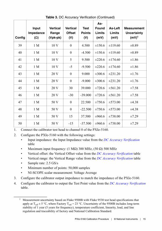
Table 3. DC Accuracy Verification (Continued)
Config
InputImpedance
(Ω)
VerticalRange
(Vpk-pk)
VerticalOffset
(V)
TestPoints
(V)
As-FoundLimits(mV)
As-LeftLimits(mV)
MeasurementUncertainty
(mV)1
39 1 M 10 V 0 4.500 ±150.6 ±119.60 ±0.89
40 1 M 10 V 0 -4.500 ±150.6 ±119.60 ±0.89
41 1 M 10 V 5 9.500 ±220.6 ±174.60 ±1.86
42 1 M 10 V -5 -9.500 ±220.6 ±174.60 ±1.86
43 1 M 20 V 0 9.000 ±300.6 ±231.20 ±1.76
44 1 M 20 V 0 -9.000 ±300.6 ±231.20 ±1.76
45 1 M 20 V 30 39.000 ±720.6 ±561.20 ±7.58
46 1 M 20 V -30 -39.000 ±720.6 ±561.20 ±7.58
47 1 M 50 V 0 22.500 ±750.6 ±573.00 ±4.38
48 1 M 50 V 0 -22.500 ±750.6 ±573.00 ±4.38
49 1 M 50 V 15 37.500 ±960.6 ±738.00 ±7.29
50 1 M 50 V -15 -37.500 ±960.6 ±738.00 ±7.29
1. Connect the calibrator test head to channel 0 of the PXIe-5160.2. Configure the PXIe-5160 with the following settings:
• Input impedance: the Input Impedance value from the DC Accuracy Verificationtable
• Maximum input frequency: (1 MΩ) 300 MHz, (50 Ω) 500 MHz• Vertical offset: the Vertical Offset value from the DC Accuracy Verification table• Vertical range: the Vertical Range value from the DC Accuracy Verification table• Sample rate: 2.5 GS/s• Minimum number of points: 50,000 samples• NI-SCOPE scalar measurement: Voltage Average
3. Configure the calibrator output impedance to match the impedance of the PXIe-5160.4. Configure the calibrator to output the Test Point value from the DC Accuracy Verification
table.
1 Measurement uncertainty based on Fluke 9500B with Fluke 9530 test head specifications thatapply at Tcal ± 5 °C, where Factory Tcal = 23 °C. Uncertainty of the 9500B includes long-termstability of 1 year (5 years for frequency), temperature coefficient, linearity, load, and lineregulation and traceability of factory and National Calibration Standard.
PXIe-5160 Calibration Procedure | © National Instruments | 15

5. Enable the calibrator output.6. Wait one second for settling, then record the measured voltage.7. Use the following formula to calculate the voltage error:
DC voltage error = Vmeasured - Test Point8. Compare the voltage error to the appropriate limit from the DC Accuracy Verification
table.9. Change the maximum input frequency to 175 MHz and repeat steps 6 through 8.10. Change the maximum input frequency to 20 MHz and repeat steps 6 through 8.11. Configure the device with the following settings and repeat steps 6 through 10:
• Maximum input frequency: (1 MΩ) 300 MHz, (50 Ω) 500 MHz• Sample rate: 1.25 GS/s
12. Repeat steps 2 through 11 for each configuration listed in the DC Accuracy Verificationtable.
13. Connect the calibrator test head to channel 1 of the PXIe-5160 and repeat steps 2 through11 for each configuration listed in the DC Accuracy Verification table.
Note If you are verifying the PXIe-5160 (4CH), proceed to the following step.If you are verifying the PXIe-5160 (2CH), DC accuracy verification iscomplete.
14. Connect the calibrator test head to channel 2 of the PXIe-5160 and repeat steps 2 through11 for each configuration listed in the DC Accuracy Verification table.
15. Connect the calibrator test head to channel 3 of the PXIe-5160 and repeat steps 2 through11 for each configuration listed in the DC Accuracy Verification table.
Verifying AC Amplitude AccuracyFollow this procedure to verify the AC amplitude accuracy of the PXIe-5160 by comparing thevoltage measured by the PXIe-5160 to the voltage measured by the DMM.
Refer to the following table as you complete the following steps:
16 | ni.com | PXIe-5160 Calibration Procedure

Table 4. AC Amplitude Accuracy Verification
Config
InputImpedance
(Ω)
VerticalRange
(Vpk-pk)
TestPoint
(Vpk-pk)Frequency
(kHz)
DMMRange(Vrms)
As-FoundLimits(dB)
As-Left
Limits(dB)
MeasurementUncertainty
(dB)2
1 50 0.2 V 0.14 50.0 0.05 ±0.50 ±0.39 ±0.014
2 50 0.5 V 0.35 50.0 0.5 ±0.50 ±0.39 ±0.018
3 50 1 V 0.7 50.0 0.5 ±0.50 ±0.39 ±0.014
4 50 2 V 1.4 50.0 0.5 ±0.50 ±0.39 ±0.012
5 50 5 V 3.5 50.0 5.0 ±0.50 ±0.39 ±0.018
6 1 M 0.2 V 0.14 50.0 0.05 ±0.50 ±0.41 ±0.013
7 1 M 0.5 V 0.35 50.0 0.5 ±0.50 ±0.41 ±0.017
8 1 M 1 V 0.7 50.0 0.5 ±0.50 ±0.41 ±0.013
9 1 M 2 V 1.4 50.0 0.5 ±0.50 ±0.41 ±0.011
10 1 M 5 V 3.5 50.0 5.0 ±0.50 ±0.41 ±0.017
11 1 M 10 V 7 50.0 5.0 ±0.50 ±0.41 ±0.013
12 1 M 20 V 14 50.0 5.0 ±0.50 ±0.41 ±0.011
13 1 M 50 V 20 50.0 50.0 ±0.50 ±0.41 ±0.024
2 Measurement Uncertainty is based on the following equipment and conditions:• NI PXI-4070 specifications apply after self-calibration is performed, in an ambient
temperature of 23 °C ± 10 °C, with 6.5 digit resolution, a measurement aperture greater than80 μs, and Auto Zero enabled
• The cable from the BNC Tee to the DMM must be 1 meter or less• Pasternack BNC Tee PE9174
PXIe-5160 Calibration Procedure | © National Instruments | 17
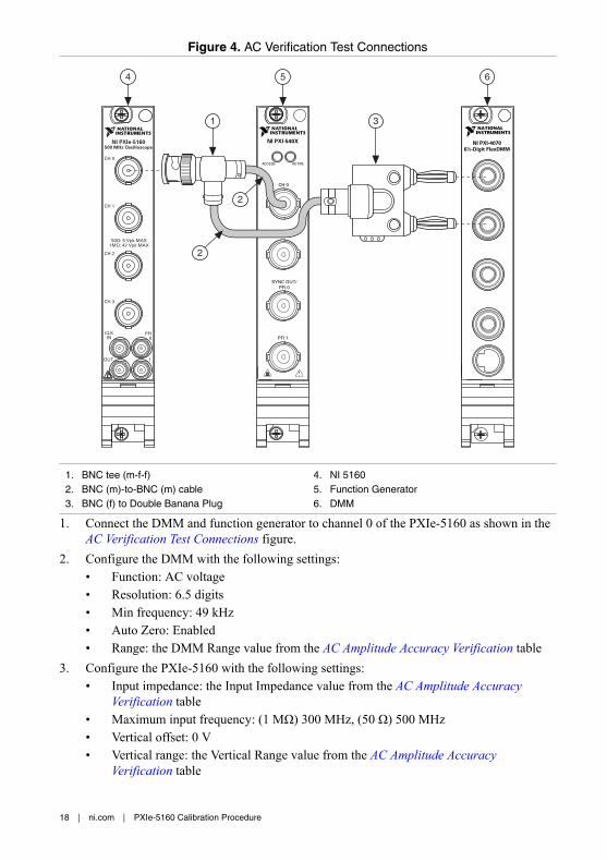
Figure 4. AC Verification Test Connections
CH 0
50Ω: 5 Vpk MAX1MΩ: 42 Vpk MAX
CH 1
CH 2
CLKIN
PFI0
1OUT
NI PXIe-5160500 MHz Oscilloscope
CH 3
ACCESS ACTIVE
SYNC OUT/PFI 0
PFI 1
NI PXI-540X
REF IN
CH 0
NI PXI-40706½-Digit FlexDMM
2
1 3
2
4 5 6
1. BNC tee (m-f-f)2. BNC (m)-to-BNC (m) cable3. BNC (f) to Double Banana Plug
4. NI 51605. Function Generator6. DMM
1. Connect the DMM and function generator to channel 0 of the PXIe-5160 as shown in the AC Verification Test Connections figure.
2. Configure the DMM with the following settings:• Function: AC voltage• Resolution: 6.5 digits• Min frequency: 49 kHz• Auto Zero: Enabled• Range: the DMM Range value from the AC Amplitude Accuracy Verification table
3. Configure the PXIe-5160 with the following settings:• Input impedance: the Input Impedance value from the AC Amplitude Accuracy
Verification table• Maximum input frequency: (1 MΩ) 300 MHz, (50 Ω) 500 MHz• Vertical offset: 0 V• Vertical range: the Vertical Range value from the AC Amplitude Accuracy
Verification table
18 | ni.com | PXIe-5160 Calibration Procedure

• Sample clock timebase source: VAL_INTERNAL_TIMEBASE• Sample rate: 2.5 GS/s• Sample clock timebase multiplier: 2• Sample clock timebase divisor: 200• Minimum number of points: 50,000 samples• NI-SCOPE scalar measurement: AC Estimate
Note The actual sample rate of the PXIe-5160 is calculated by the followingformula:25 MS/s = (Sample clock timebase rate × Sample clock timebase multiplier) /Sample clock timebase divisor
Note Setting the Sample clock timebase attribute keeps the PXIe-5160 in thedesired configuration even when data decimation is needed to measure theamplitude of the 50 kHz sine wave.
4. Configure the function generator and generate a waveform with the followingcharacteristics:• Waveform: Sine wave• Amplitude: the Test Point value from the AC Amplitude Accuracy Verification table• Frequency: 50 kHz• Load impedance: the Input Impedance value from the AC Amplitude Accuracy
Verification table
Note These values assume you are using a NI 5402 function generator. Forother function generators, the output voltage varies with load output impedance,up to doubling the voltage for a high impedance load.
5. Wait 1 second for the output of the function generator to settle.6. Measure the output voltage amplitude using the PXIe-5160 and the DMM.7. Record the Vrms measurements.8. Calculate the amplitude error using the following formula:
AC Voltage Error = 20 × log10(VPXIe-5160 Measured/VDMM Measured)9. Compare the amplitude error to the appropriate Limit from the AC Amplitude Accuracy
Verification table10. Change the maximum input frequency to 175 MHz and repeat steps 5 through 9.11. Change the maximum input frequency to 20 MHz and repeat steps 5 through 9.12. Configure the device with the following settings and repeat steps 5 through 11:
• Maximum input frequency: (1 MΩ) 300 MHz, (50 Ω) 500 MHz• Sample clock timebase multiplier: 1• Sample clock timebase divisor: 100
13. Repeat steps 2 through 12 for each configuration listed in the AC Amplitude AccuracyVerification table.
PXIe-5160 Calibration Procedure | © National Instruments | 19
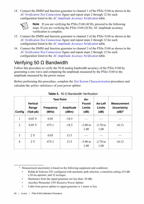
14. Connect the DMM and function generator to channel 1 of the PXIe-5160 as shown in the AC Verification Test Connections figure and repeat steps 2 through 12 for eachconfiguration listed in the AC Amplitude Accuracy Verification table.
Note If you are verifying the PXIe-5160 (4CH), proceed to the followingsteps. If you are verifying the PXIe-5160 (2CH), AC amplitude accuracyverification is complete.
15. Connect the DMM and function generator to channel 2 of the PXIe-5160 as shown in the AC Verification Test Connections figure and repeat steps 2 through 12 for eachconfiguration listed in the AC Amplitude Accuracy Verification table.
16. Connect the DMM and function generator to channel 3 of the PXIe-5160 as shown in the AC Verification Test Connections figure and repeat steps 2 through 12 for eachconfiguration listed in the AC Amplitude Accuracy Verification table.
Verifying 50 Ω BandwidthFollow this procedure to verify the 50 Ω analog bandwidth accuracy of the PXIe-5160 bygenerating a sine wave and comparing the amplitude measured by the PXIe-5160 to theamplitude measured by the power sensor.
Before performing this procedure, complete the Test System Characterization procedures andcalculate the splitter imbalance of your power splitter.
Table 5. 50 Ω Bandwidth Verification
Config
VerticalRange
(Vpk-pk)
Test Point As-FoundLimits(dB)
As-LeftLimits(dB)
MeasurementUncertainty
(dB)3
Frequency(MHz)
Amplitude(dBm)
1 0.05 V 0.05 -18.5 — — —
2 0.05 V 475.1 -18.5 -3.00 to1.00
-2.70 to1.00
±0.13
3 2 V 0.05 13.5 — — —
4 2 V 475.1 13.5 -3.00 to1.00
-2.70 to1.00
±0.13
3 Measurement uncertainty is based on the following equipment and conditions:• Rohde & Schwarz Z91 configured with automatic path selection, a transition setting of 0 dB,
a 20 ms aperture, and 32 averages.• Harmonics from the signal generator are less than -30 dBc• Aeroflex/Weinschel 1593 Resistive Power Splitter• Cable from power splitter to signal generator is 1 meter or less
20 | ni.com | PXIe-5160 Calibration Procedure

1. Connect splitter output 2 of the power sensor assembly from the Test SystemCharacterization section to channel 0 of the PXIe-5160.
Note The power sensor assembly must match the configuration used in the Test System Characterization section, in which the power sensor is connected tosplitter output 1 and the signal generator is connected to the input port of thepower splitter.
The following figure illustrates the hardware setup.
Figure 5. 50 Ω Bandwidth Verification Cabling Diagram
6
8
CH 0
50Ω: 5 Vpk MAX1MΩ: 42 Vpk MAX
CH 1
TRIG
CLKIN
PFI0
1OUT
NI PXIe-5160500 MHz Oscilloscope
7
2
1
3
4
3
5
1. Power Sensor2. BNC (f)-to-N (f) Adapter3. SMA (m)-to-BNC (m) Adapter4. Power Splitter
5. NI 51606. SMA (m)-to-SMA (m) Cable7. SMA (f)-to-N (m) Cable8. Signal Generator
PXIe-5160 Calibration Procedure | © National Instruments | 21
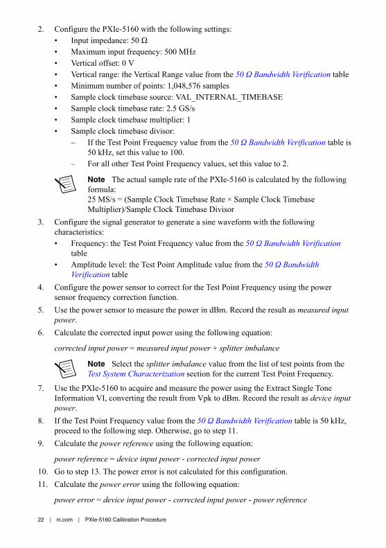
2. Configure the PXIe-5160 with the following settings:• Input impedance: 50 Ω• Maximum input frequency: 500 MHz• Vertical offset: 0 V• Vertical range: the Vertical Range value from the 50 Ω Bandwidth Verification table• Minimum number of points: 1,048,576 samples• Sample clock timebase source: VAL_INTERNAL_TIMEBASE• Sample clock timebase rate: 2.5 GS/s• Sample clock timebase multiplier: 1• Sample clock timebase divisor:
– If the Test Point Frequency value from the 50 Ω Bandwidth Verification table is50 kHz, set this value to 100.
– For all other Test Point Frequency values, set this value to 2.
Note The actual sample rate of the PXIe-5160 is calculated by the followingformula:25 MS/s = (Sample Clock Timebase Rate × Sample Clock TimebaseMultiplier)/Sample Clock Timebase Divisor
3. Configure the signal generator to generate a sine waveform with the followingcharacteristics:• Frequency: the Test Point Frequency value from the 50 Ω Bandwidth Verification
table• Amplitude level: the Test Point Amplitude value from the 50 Ω Bandwidth
Verification table4. Configure the power sensor to correct for the Test Point Frequency using the power
sensor frequency correction function.5. Use the power sensor to measure the power in dBm. Record the result as measured input
power.6. Calculate the corrected input power using the following equation:
corrected input power = measured input power + splitter imbalance
Note Select the splitter imbalance value from the list of test points from the Test System Characterization section for the current Test Point Frequency.
7. Use the PXIe-5160 to acquire and measure the power using the Extract Single ToneInformation VI, converting the result from Vpk to dBm. Record the result as device inputpower.
8. If the Test Point Frequency value from the 50 Ω Bandwidth Verification table is 50 kHz,proceed to the following step. Otherwise, go to step 11.
9. Calculate the power reference using the following equation:
power reference = device input power - corrected input power10. Go to step 13. The power error is not calculated for this configuration.11. Calculate the power error using the following equation:
power error = device input power - corrected input power - power reference
22 | ni.com | PXIe-5160 Calibration Procedure
12. Compare the power error to the appropriate Limit from the 50 Ω Bandwidth Verificationtable.
13. Repeat steps 2 through 12 for each configuration in the 50 Ω Bandwidth Verificationtable.
14. Connect splitter output 2 of the power sensor assembly to channel 1 of the PXIe-5160 andrepeat steps 2 through 12 for each configuration listed in the 50 Ω Bandwidth Verificationtable.
Note If you are verifying the PXIe-5160 (4CH), proceed to the followingsteps. If you are verifying the PXIe-5160 (2CH), 50 Ω bandwidth verification iscomplete.
15. Connect splitter output 2 of the power sensor assembly to channel 2 of the PXIe-5160 andrepeat steps 2 through 12 for each configuration listed in the 50 Ω Bandwidth Verificationtable.
16. Connect splitter output 2 of the power sensor assembly to channel 3 of the PXIe-5160 andrepeat steps 2 through 12 for each configuration listed in the 50 Ω Bandwidth Verificationtable.
Verifying 1 MΩ BandwidthFollow this procedure to verify the 1 MΩ analog bandwidth accuracy of the PXIe-5160 bygenerating a sine wave and comparing the amplitude measured by the PXIe-5160 to theamplitude measured by the power sensor.
Before performing this procedure, complete the Test System Characterization procedures andcalculate the splitter imbalance of your power splitter.
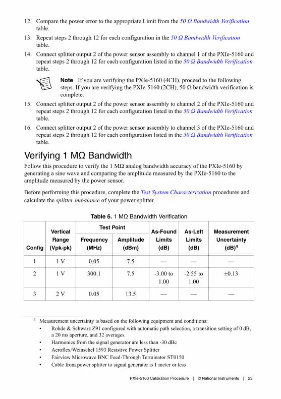
Table 6. 1 MΩ Bandwidth Verification
Config
VerticalRange
(Vpk-pk)
Test PointAs-Found
Limits(dB)
As-LeftLimits(dB)
MeasurementUncertainty
(dB)4
Frequency(MHz)
Amplitude(dBm)
1 1 V 0.05 7.5 — — —
2 1 V 300.1 7.5 -3.00 to1.00
-2.55 to1.00
±0.13
3 2 V 0.05 13.5 — — —
4 Measurement uncertainty is based on the following equipment and conditions:• Rohde & Schwarz Z91 configured with automatic path selection, a transition setting of 0 dB,
a 20 ms aperture, and 32 averages.• Harmonics from the signal generator are less than -30 dBc• Aeroflex/Weinschel 1593 Resistive Power Splitter• Fairview Microwave BNC Feed-Through Terminator ST0150• Cable from power splitter to signal generator is 1 meter or less
PXIe-5160 Calibration Procedure | © National Instruments | 23

Table 6. 1 MΩ Bandwidth Verification (Continued)
Config
VerticalRange
(Vpk-pk)
Test PointAs-Found
Limits(dB)
As-LeftLimits(dB)
MeasurementUncertainty
(dB)4
Frequency(MHz)
Amplitude(dBm)
4 2 V 250.1 13.5 -3.00 to1.00
-2.68 to1.00
±0.11
5 10 V 0.05 16 — — —
6 10 V 250.1 16 -3.00 to1.00
-2.68 to1.00
±0.11
1. Connect the 50 Ω BNC feed-through terminator to channel 0 of the PXIe-5160. Connectsplitter output 2 of the power sensor assembly from the Test System Characterizationsection to the 50 Ω BNC feed-through terminator.
Note The power sensor assembly must match the configuration used in the Test System Characterization section, in which the power sensor is connected tosplitter output 1 and the signal generator is connected to the input port of thepower splitter.
The following figure illustrates the hardware setup.
4 Measurement uncertainty is based on the following equipment and conditions:• Rohde & Schwarz Z91 configured with automatic path selection, a transition setting of 0 dB,
a 20 ms aperture, and 32 averages.• Harmonics from the signal generator are less than -30 dBc• Aeroflex/Weinschel 1593 Resistive Power Splitter• Fairview Microwave BNC Feed-Through Terminator ST0150• Cable from power splitter to signal generator is 1 meter or less
24 | ni.com | PXIe-5160 Calibration Procedure
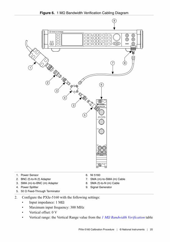
Figure 6. 1 MΩ Bandwidth Verification Cabling Diagram
CH 0
50Ω: 5 Vpk MAX1MΩ: 42 Vpk MAX
CH 1
TRIG
CLKIN
PFI0
1OUT
NI PXIe-5160500 MHz Oscilloscope
7
6
9
8
2
1
3
4
5
3
1. Power Sensor2. BNC (f)-to-N (f) Adapter3. SMA (m)-to-BNC (m) Adapter4. Power Splitter5. 50 Ω Feed-Through Terminator
6. NI 51607. SMA (m)-to-SMA (m) Cable8. SMA (f)-to-N (m) Cable9. Signal Generator
2. Configure the PXIe-5160 with the following settings:• Input impedance: 1 MΩ• Maximum input frequency: 300 MHz• Vertical offset: 0 V• Vertical range: the Vertical Range value from the 1 MΩ Bandwidth Verification table
PXIe-5160 Calibration Procedure | © National Instruments | 25

• Minimum number of points: 1,048,576 samples• Sample clock timebase source: VAL_INTERNAL_TIMEBASE• Sample clock timebase rate: 2.5 GS/s• Sample clock timebase multiplier: 1• Sample clock timebase divisor:
– If the Test Point Frequency value from the 1 MΩ Bandwidth Verification tableis 50 kHz, set this value to 100.
– For all other Test Point Frequency values, set this value to 2.
Note The actual sample rate of the PXIe-5160 is calculated by the followingformula:25 MS/s = (Sample Clock Timebase Rate × Sample Clock TimebaseMultiplier)/Sample Clock Timebase Divisor
3. Configure the signal generator to generate a sine waveform with the followingcharacteristics:• Frequency: the Test Point Frequency value from the 1 MΩ Bandwidth Verification
table• Amplitude level: the Test Point Amplitude value from the 1 MΩ Bandwidth
Verification table4. Configure the power sensor to correct for the Test Point Frequency using the power
sensor frequency correction function.5. Use the power sensor to measure the power in dBm. Record the result as measured input
power.6. Calculate the corrected input power using the following equation:
corrected input power = measured input power + splitter imbalance
Note Select the splitter imbalance value from the list of test points from the Test System Characterization section for the current Test Point Frequency.
7. Use the PXIe-5160 to acquire and measure the power using the Extract Single ToneInformation VI, converting the result from Vpk to dBm. Record the result as device inputpower.
8. If the Test Point Frequency value from the 1 MΩ Bandwidth Verification table is 50 kHz,proceed to the following step. Otherwise, go to step 11.
9. Calculate the power reference using the following equation:
power reference = device input power - corrected input power10. Go to step 13. The power error is not calculated for this configuration.11. Calculate the power error using the following equation:
power error = device input power - corrected input power - power reference12. Compare the power error to the appropriate Limit from the 1 MΩ Bandwidth Verification
table.13. Repeat steps 2 through 12 for each configuration in the 1 MΩ Bandwidth Verification
table.
26 | ni.com | PXIe-5160 Calibration Procedure

14. Connect the 50 Ω BNC feed-through terminator to channel 1 of the PXIe-5160. Connectsplitter output 2 of the power sensor assembly to the 50 Ω BNC feed-through terminatorand repeat steps 2 through 12 for each configuration in the 1 MΩ Bandwidth Verificationtable.
Note If you are verifying the PXIe-5160 (4CH), proceed to the followingsteps. If you are verifying the PXIe-5160 (2CH), 1 MΩ bandwidth verificationis complete.
15. Connect the 50 Ω BNC feed-through terminator to channel 2 of the PXIe-5160. Connectsplitter output 2 of the power sensor assembly to the 50 Ω BNC feed-through terminatorand repeat steps 2 through 12 for each configuration in the 1 MΩ Bandwidth Verificationtable.
16. Connect the 50 Ω BNC feed-through terminator to channel 3 of the PXIe-5160. Connectsplitter output 2 of the power sensor assembly to the 50 Ω BNC feed-through terminatorand repeat steps 2 through 12 for each configuration in the 1 MΩ Bandwidth Verificationtable.
Verifying Timebase AccuracyFollow this procedure to verify the frequency accuracy of the PXIe-5160 onboard timebaseusing an oscilloscope calibrator.
Table 7. Timebase Accuracy Verification
Test Limits Measurement Uncertainty
±25 PPM (±2,500 Hz) ±0.2 PPM (±20 Hz)
1. Connect the calibrator test head to channel 0 of the PXIe-5160.2. Configure the PXIe-5160 with the following settings:
• Input impedance: 50 Ω• Maximum input frequency: 500 MHz• Vertical range: 1 Vpk-pk• Sample rate: 1.25 GS/s• Minimum number of points: 1,048,576 samples
3. Configure the calibrator and generate a waveform with the following characteristics:• Waveform: Sine wave• Amplitude (Vpk-pk): 0.9 V• Frequency: 100 MHz• Load impedance: 50 Ω
4. Enable the calibrator output.5. Wait 1 second for settling, then measure and record the peak frequency using the Extract
Single Tone Information VI.
5 Measurement uncertainty based on Fluke 9500B with Fluke 9530 test head specifications thatapply at Tcal ±5 °C, where Factory Tcal = 23 °C. Uncertainty of the 9500B includes long-termstability of 1 year (5 years for frequency), temperature coefficient, linearity, load, and lineregulation and traceability of factory and National Calibration Standard.
PXIe-5160 Calibration Procedure | © National Instruments | 27

6. Calculate the timebase error using the following formula:
Timebase error = (Fmeasured - (100 × 106))/1007. Compare the timebase error to the appropriate limit from the Timebase Accuracy
Verification table.
Note Timebase verification is only required on one channel.
8. Disable the calibrator output.
Verifying Input ImpedanceFollow this procedure to verify the input impedance of the PXIe-5160 using an oscilloscopecalibrator.
Table 8. Input Impedance Verification
ConfigVertical Range
(Vpk-pk)Input
Impedance (Ω)
As-FoundTest Limits
(Ω)
As-LeftTest Limits
(Ω)Measurement
Uncertainty (Ω)
1 1 V 50 ±0.875 ±0.48 ±0.045
2 2 V 50 ±0.875 ±0.48 ±0.045
3 1 V 1 M ±9000 ±7000 ±775
4 10 V 1 M ±9000 ±7000 ±775
5 20 V 1 M ±9000 ±7000 ±775
1. Connect the calibrator test head to channel 0 of the PXIe-5160.2. Configure the PXIe-5160 with the following settings:
• Input impedance: the Input Impedance value from the Input Impedance Verificationtable.
• Maximum input frequency: (50 Ω) 500 MHz, (1 MΩ), 300 MHz• Vertical offset: 0 V• Vertical range: the Vertical Rage value from the Input Impedance Verification table.• Sample rate: 2.5 GS/s• Minimum number of points: 50,000 samples
3. Configure the calibrator output impedance to match that of the PXIe-5160.4. Configure the calibrator to measure impedance.5. Enable the calibrator.6. Wait 1 second for settling, then record the measured impedance.7. Use the following formula to calculate the input impedance error:
input impedance error = ImpedanceMeasured - Input Impedance value from the InputImpedance Verification table
28 | ni.com | PXIe-5160 Calibration Procedure
8. Compare the input impedance error to the appropriate Limit from the Input ImpedanceVerification table.
9. Repeat steps 2 through 8 for each configuration listed in the Input Impedance Verificationtable.
10. Connect the calibrator test head to channel 1 of the PXIe-5160 and repeat steps 2 through8 for each configuration listed in the Input Impedance Verification table.
Note If you are verifying the PXIe-5160 (4CH), proceed to the followingsteps. If you are verifying the PXIe-5160 (2CH), input impedance verificationis complete.
11. Connect the calibrator test head to channel 2 of the PXIe-5160 and repeat steps 2 through8 for each configuration listed in the Input Impedance Verification table.
12. Connect the calibrator test head to channel 3 of the PXIe-5160 and repeat steps 2 through8 for each configuration listed in the Input Impedance Verification table.
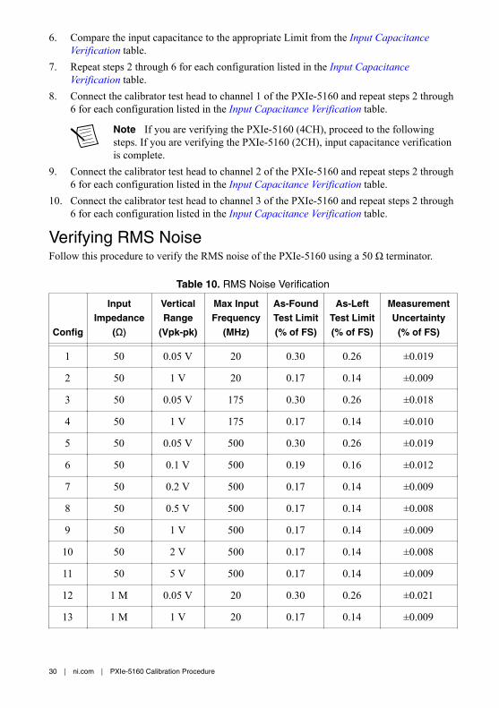
Verifying Input CapacitanceFollow this procedure to verify in the input capacitance of the PXIe-5160 using anoscilloscope calibrator.
Table 9. Input Capacitance Verification
ConfigVertical Range
(Vpk-pk)As-Found Test
Limits (pF)As-Left TestLimits (pF)
MeasurementUncertainty (pF)6
0 1 V 12.5 to 17.5 12.9 to 17.1 ±0.46
1 10 V 12.5 to 17.5 12.9 to 17.1 ±0.46
2 20 V 12.5 to 17.5 12.9 to 17.1 ±0.46
1. Connect the calibrator test head to channel 0 of the PXIe-5160.2. Configure the PXIe-5160 with the following settings:
• Input impedance: 1 MΩ• Maximum input frequency: 300 MHz• Vertical offset: 0 V• Vertical range: the Vertical Range value from the Input Capacitance Verification
table• Sample rate: 2.5 GS/s• Minimum number of points: 50,000 samples
3. Configure the calibrator to measure capacitance.4. Enable the calibrator.5. Wait 1 second for settling, then record the measured capacitance.
6 Measurement uncertainty based on Fluke 9500B with Fluke 9530 test head specifications thatapply at Tcal ± 5 °C, where Factory Tcal = 23 °C. Uncertainty of the 9500B includes long-termstability of 1 year (5 years for frequency), temperature coefficient, linearity, load, and lineregulation and traceability of factory and National Calibration Standard.
PXIe-5160 Calibration Procedure | © National Instruments | 29
6. Compare the input capacitance to the appropriate Limit from the Input CapacitanceVerification table.
7. Repeat steps 2 through 6 for each configuration listed in the Input CapacitanceVerification table.
8. Connect the calibrator test head to channel 1 of the PXIe-5160 and repeat steps 2 through6 for each configuration listed in the Input Capacitance Verification table.
Note If you are verifying the PXIe-5160 (4CH), proceed to the followingsteps. If you are verifying the PXIe-5160 (2CH), input capacitance verificationis complete.
9. Connect the calibrator test head to channel 2 of the PXIe-5160 and repeat steps 2 through6 for each configuration listed in the Input Capacitance Verification table.
10. Connect the calibrator test head to channel 3 of the PXIe-5160 and repeat steps 2 through6 for each configuration listed in the Input Capacitance Verification table.
Verifying RMS NoiseFollow this procedure to verify the RMS noise of the PXIe-5160 using a 50 Ω terminator.
Table 10. RMS Noise Verification
Config
InputImpedance
(Ω)
VerticalRange
(Vpk-pk)
Max InputFrequency
(MHz)
As-FoundTest Limit(% of FS)
As-LeftTest Limit(% of FS)
MeasurementUncertainty
(% of FS)
1 50 0.05 V 20 0.30 0.26 ±0.019
2 50 1 V 20 0.17 0.14 ±0.009
3 50 0.05 V 175 0.30 0.26 ±0.018
4 50 1 V 175 0.17 0.14 ±0.010
5 50 0.05 V 500 0.30 0.26 ±0.019
6 50 0.1 V 500 0.19 0.16 ±0.012
7 50 0.2 V 500 0.17 0.14 ±0.009
8 50 0.5 V 500 0.17 0.14 ±0.008
9 50 1 V 500 0.17 0.14 ±0.009
10 50 2 V 500 0.17 0.14 ±0.008
11 50 5 V 500 0.17 0.14 ±0.009
12 1 M 0.05 V 20 0.30 0.26 ±0.021
13 1 M 1 V 20 0.17 0.14 ±0.009
30 | ni.com | PXIe-5160 Calibration Procedure
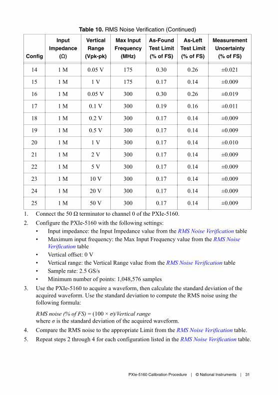
Table 10. RMS Noise Verification (Continued)
Config
InputImpedance
(Ω)
VerticalRange
(Vpk-pk)
Max InputFrequency
(MHz)
As-FoundTest Limit(% of FS)
As-LeftTest Limit(% of FS)
MeasurementUncertainty
(% of FS)
14 1 M 0.05 V 175 0.30 0.26 ±0.021
15 1 M 1 V 175 0.17 0.14 ±0.009
16 1 M 0.05 V 300 0.30 0.26 ±0.019
17 1 M 0.1 V 300 0.19 0.16 ±0.011
18 1 M 0.2 V 300 0.17 0.14 ±0.009
19 1 M 0.5 V 300 0.17 0.14 ±0.009
20 1 M 1 V 300 0.17 0.14 ±0.010
21 1 M 2 V 300 0.17 0.14 ±0.009
22 1 M 5 V 300 0.17 0.14 ±0.009
23 1 M 10 V 300 0.17 0.14 ±0.009
24 1 M 20 V 300 0.17 0.14 ±0.009
25 1 M 50 V 300 0.17 0.14 ±0.009
1. Connect the 50 Ω terminator to channel 0 of the PXIe-5160.2. Configure the PXIe-5160 with the following settings:
• Input impedance: the Input Impedance value from the RMS Noise Verification table• Maximum input frequency: the Max Input Frequency value from the RMS Noise
Verification table• Vertical offset: 0 V• Vertical range: the Vertical Range value from the RMS Noise Verification table• Sample rate: 2.5 GS/s• Minimum number of points: 1,048,576 samples
3. Use the PXIe-5160 to acquire a waveform, then calculate the standard deviation of theacquired waveform. Use the standard deviation to compute the RMS noise using thefollowing formula:
RMS noise (% of FS) = (100 × σ)/Vertical rangewhere σ is the standard deviation of the acquired waveform.
4. Compare the RMS noise to the appropriate Limit from the RMS Noise Verification table.5. Repeat steps 2 through 4 for each configuration listed in the RMS Noise Verification table.
PXIe-5160 Calibration Procedure | © National Instruments | 31

6. Connect the 50 Ω terminator to channel 1 of the PXIe-5160 and repeat steps 2 through 4for each configuration listed in the RMS Noise Verification table.
Note If you are verifying the PXIe-5160 (4CH), proceed to the followingsteps. If you are verifying the PXIe-5160 (2CH), RMS noise verification iscomplete.
7. Connect the 50 Ω terminator to channel 2 of the PXIe-5160 and repeat steps 2 through 4for each configuration listed in the RMS Noise Verification table.
8. Connect the 50 Ω terminator to channel 3 of the PXIe-5160 and repeat steps 2 through 4for each configuration listed in the RMS Noise Verification table.
AdjustmentFollow this procedure to externally adjust the PXIe-5160.
Table 11. Vertical Range Adjustment
Config Input Impedance (Ω) Vertical Range (Vpk-pk) Input (V)
1 1 M 50 V 22.500
2 1 M 50 V -22.500
3 1 M 20 V 9.000
4 1 M 20 V -9.000
5 1 M 10 V 4.500
6 1 M 10 V -4.500
7 1 M 5 V 2.250
8 1 M 5 V -2.250
9 1 M 2 V 0.900
10 1 M 2 V -0.900
11 1 M 1 V 0.450
12 1 M 1 V -0.450
13 1 M 0.631 V 0.284
14 1 M 0.631 V -0.284
15 1 M 0.5 V 0.225
16 1 M 0.5 V -0.225
17 1 M 0.2 V 0.090
32 | ni.com | PXIe-5160 Calibration Procedure

Table 11. Vertical Range Adjustment (Continued)
Config Input Impedance (Ω) Vertical Range (Vpk-pk) Input (V)
18 1 M 0.2 V -0.090
19 1 M 0.1 V 0.045
20 1 M 0.1 V -0.045
21 1 M 0.05 V 0.023
22 1 M 0.05 V -0.023
23 50 0.05 V 0.023
24 50 0.05 V -0.023
25 50 0.1 V 0.045
26 50 0.1 V -0.045
27 50 0.2 V 0.090
28 50 0.2 V -0.090
29 50 0.5 V 0.225
30 50 0.5 V -0.225
31 50 0.631 V 0.284
32 50 0.631 V -0.284
33 50 1 V 0.450
34 50 1 V -0.450
35 50 2 V 0.900
36 50 2 V -0.900
37 50 5 V 2.250
38 50 5 V -2.250
Table 12. 1 MΩ Compensation Attenuator Adjustment
Config Input Impedance (Ω) Vertical Range (Vpk-pk) Input (V)
1 1 M 1 V 0.500
2 1 M 1 V 0.900
PXIe-5160 Calibration Procedure | © National Instruments | 33
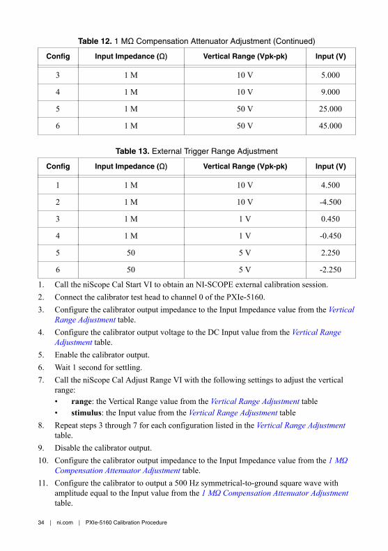
Table 12. 1 MΩ Compensation Attenuator Adjustment (Continued)
Config Input Impedance (Ω) Vertical Range (Vpk-pk) Input (V)
3 1 M 10 V 5.000
4 1 M 10 V 9.000
5 1 M 50 V 25.000
6 1 M 50 V 45.000
Table 13. External Trigger Range Adjustment
Config Input Impedance (Ω) Vertical Range (Vpk-pk) Input (V)
1 1 M 10 V 4.500
2 1 M 10 V -4.500
3 1 M 1 V 0.450
4 1 M 1 V -0.450
5 50 5 V 2.250
6 50 5 V -2.250
1. Call the niScope Cal Start VI to obtain an NI-SCOPE external calibration session.2. Connect the calibrator test head to channel 0 of the PXIe-5160.3. Configure the calibrator output impedance to the Input Impedance value from the Vertical
Range Adjustment table.4. Configure the calibrator output voltage to the DC Input value from the Vertical Range
Adjustment table.5. Enable the calibrator output.6. Wait 1 second for settling.7. Call the niScope Cal Adjust Range VI with the following settings to adjust the vertical
range:• range: the Vertical Range value from the Vertical Range Adjustment table• stimulus: the Input value from the Vertical Range Adjustment table
8. Repeat steps 3 through 7 for each configuration listed in the Vertical Range Adjustmenttable.
9. Disable the calibrator output.10. Configure the calibrator output impedance to the Input Impedance value from the 1 MΩ
Compensation Attenuator Adjustment table.11. Configure the calibrator to output a 500 Hz symmetrical-to-ground square wave with
amplitude equal to the Input value from the 1 MΩ Compensation Attenuator Adjustmenttable.
34 | ni.com | PXIe-5160 Calibration Procedure
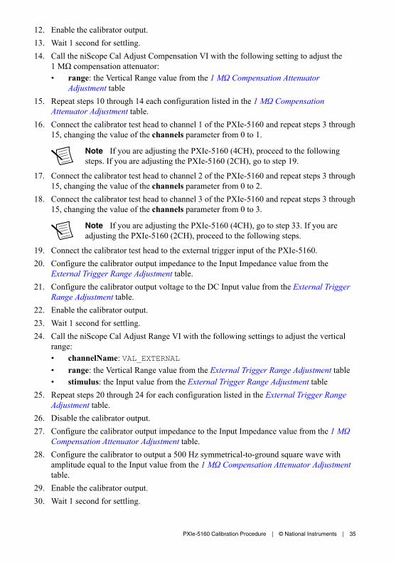
12. Enable the calibrator output.13. Wait 1 second for settling.14. Call the niScope Cal Adjust Compensation VI with the following setting to adjust the
1 MΩ compensation attenuator:• range: the Vertical Range value from the 1 MΩ Compensation Attenuator
Adjustment table15. Repeat steps 10 through 14 each configuration listed in the 1 MΩ Compensation
Attenuator Adjustment table.16. Connect the calibrator test head to channel 1 of the PXIe-5160 and repeat steps 3 through
15, changing the value of the channels parameter from 0 to 1.
Note If you are adjusting the PXIe-5160 (4CH), proceed to the followingsteps. If you are adjusting the PXIe-5160 (2CH), go to step 19.
17. Connect the calibrator test head to channel 2 of the PXIe-5160 and repeat steps 3 through15, changing the value of the channels parameter from 0 to 2.
18. Connect the calibrator test head to channel 3 of the PXIe-5160 and repeat steps 3 through15, changing the value of the channels parameter from 0 to 3.
Note If you are adjusting the PXIe-5160 (4CH), go to step 33. If you areadjusting the PXIe-5160 (2CH), proceed to the following steps.
19. Connect the calibrator test head to the external trigger input of the PXIe-5160.20. Configure the calibrator output impedance to the Input Impedance value from the
External Trigger Range Adjustment table.21. Configure the calibrator output voltage to the DC Input value from the External Trigger
Range Adjustment table.22. Enable the calibrator output.23. Wait 1 second for settling.24. Call the niScope Cal Adjust Range VI with the following settings to adjust the vertical
range:• channelName: VAL_EXTERNAL• range: the Vertical Range value from the External Trigger Range Adjustment table• stimulus: the Input value from the External Trigger Range Adjustment table
25. Repeat steps 20 through 24 for each configuration listed in the External Trigger RangeAdjustment table.
26. Disable the calibrator output.27. Configure the calibrator output impedance to the Input Impedance value from the 1 MΩ
Compensation Attenuator Adjustment table.28. Configure the calibrator to output a 500 Hz symmetrical-to-ground square wave with
amplitude equal to the Input value from the 1 MΩ Compensation Attenuator Adjustmenttable.
29. Enable the calibrator output.30. Wait 1 second for settling.
PXIe-5160 Calibration Procedure | © National Instruments | 35

31. Call the niScope Cal Adjust Compensation Attenuator VI with the following settings toadjust the 1 MΩ compensation attenuator:• channelName: VAL_EXTERNAL• range: the Vertical Range value from the 1 MΩ Compensation Attenuator
Adjustment table32. Repeat steps 27 through 31 for each configuration listed in the 1 MΩ Compensation
Attenuator Adjustment table.33. Disconnect or disable all inputs to the PXIe-5160.34. Call the niScope Cal Adjust VI with the following settings to adjust the 1 MΩ offset
range:• range: 0• stimulus: 0
35. Call the niScope Cal End VI to close the external calibration session and save thecalibration date and temperature.
36. Call the niScope Initialize VI to obtain an NI-SCOPE session.37. Self-calibrate the PXIe-5160 using the niScope Cal Self Calibrate VI.
ReverificationRepeat the Verification section to determine the as-left status of the device.
Note If any test fails reverification after performing an adjustment, verify that youhave met the Test Conditions before returning your device to NI. Refer to theWorldwide Support and Services section for information about support resources orservice requests.
Worldwide Support and ServicesThe NI website is your complete resource for technical support. At ni.com/support, you haveaccess to everything from troubleshooting and application development self-help resources toemail and phone assistance from NI Application Engineers.
Visit ni.com/services for information about the services NI offers.
Visit ni.com/register to register your NI product. Product registration facilitates technicalsupport and ensures that you receive important information updates from NI.
A Declaration of Conformity (DoC) is our claim of compliance with the Council of theEuropean Communities using the manufacturer’s declaration of conformity. This systemaffords the user protection for electromagnetic compatibility (EMC) and product safety. Youcan obtain the DoC for your product by visiting ni.com/certification. If your product supportscalibration, you can obtain the calibration certificate for your product at ni.com/calibration.
NI corporate headquarters is located at 11500 North Mopac Expressway, Austin, Texas,78759-3504. NI also has offices located around the world. For support in the United States,
36 | ni.com | PXIe-5160 Calibration Procedure

create your service request at ni.com/support or dial 1 866 ASK MYNI (275 6964). Forsupport outside the United States, visit the Worldwide Offices section of ni.com/niglobal toaccess the branch office websites, which provide up-to-date contact information.
PXIe-5160 Calibration Procedure | © National Instruments | 37

Information is subject to change without notice. Refer to the NI Trademarks and Logo Guidelines at ni.com/trademarks forinformation on NI trademarks. Other product and company names mentioned herein are trademarks or trade names of theirrespective companies. For patents covering NI products/technology, refer to the appropriate location: Help»Patents in yoursoftware, the patents.txt file on your media, or the National Instruments Patent Notice at ni.com/patents. You can findinformation about end-user license agreements (EULAs) and third-party legal notices in the readme file for your NI product. Referto the Export Compliance Information at ni.com/legal/export-compliance for the NI global trade compliance policy and howto obtain relevant HTS codes, ECCNs, and other import/export data. NI MAKES NO EXPRESS OR IMPLIED WARRANTIES ASTO THE ACCURACY OF THE INFORMATION CONTAINED HEREIN AND SHALL NOT BE LIABLE FOR ANY ERRORS. U.S.Government Customers: The data contained in this manual was developed at private expense and is subject to the applicablelimited rights and restricted data rights as set forth in FAR 52.227-14, DFAR 252.227-7014, and DFAR 252.227-7015.
© 2013—2018 National Instruments. All rights reserved.
373997G-01 March 7, 2018