
PTIC 521 Semi-Annual Letter Report
45
p PTIC ( AD-A238 521 Semi-Annual Letter Report Growth, Nitrogen Vacancy Reduction and Solid Solution Formation in Cubic GaN Thin Films and the Subsequent Fabrication of Superlattice Structures Using AIN and InN Supported under Grant #N00014-86-K-0686 P5 Innovative Science and Technology Office of the Strategic Defense Initiative Office of the Chief of Naval Research Report for the period January 1, 1991-June 30, 1991 Robert F. Davis, Michael J. Paisley and Zlatko Sitar Materials Science and Engineering Department North Carolina State University Campus Box 7907 Raleigh, NC 27695-7907 June, 1991 I 91-05475 1 %0000
Transcript of PTIC 521 Semi-Annual Letter Report

p PTIC (AD-A238 521
Semi-Annual Letter Report
Growth, Nitrogen Vacancy Reduction and Solid SolutionFormation in Cubic GaN Thin Films and the Subsequent
Fabrication of Superlattice Structures Using AIN and InN
Supported under Grant #N00014-86-K-0686 P5Innovative Science and Technology Office
of the Strategic Defense InitiativeOffice of the Chief of Naval Research
Report for the period January 1, 1991-June 30, 1991
Robert F. Davis, Michael J. Paisley and Zlatko SitarMaterials Science and Engineering Department
North Carolina State UniversityCampus Box 7907
Raleigh, NC 27695-7907
June, 1991
I 91-054751 %0000

BestAva ilable
Copy

3 1 form ApproivedREPORT DOCUMENTATION PAGE 0Me No 0 704s 6 ee8
0.0 owJto~~ " te I... 4P.a1 .141- .. A *. .. W. &I. -) .S#fSOO SIg . O -%W ltrA 6- 1)s ....^* .,... 1.40%. *~ .,,.. .1 . .a
OSSMI~at I . *..t ncjSgga4q ,.q9r%-- 'o -G .S ., 0.101.t WS~.1106 . MJ -wig ~'.P ~ si~t -0 -4-: GV~S ' 41Ke%( 4-04C1I IC0 .%S S ' ."t0O...P~q'"a. %..q* A ...... 0. 410 A"JO J i.'aSS e'd ' d ' 1.4 1 11 I ~ ~ ~ T~ ~1 A...S. C:@
1. AGENCY USE ONLY (Le-eve oidnA) 2. RE PORT DATE 3. REPORT TYPE AND OATES COVERED
I June, 1991 ISemi-Annual Letter 1/l/91-&t30/91I.4. TITLE AND SUBTITLE Growth, Nitrogen Vacancy Reduction and S. FUNDING NUMBERSsolid Solution Formation in Cubic GaN Thin Films and the R&T:s40000lsrqO5Subsequent Fabrication of Superlattice Structures Using 5.0. :1114S5AlN and InN
6. AUTHOR(S)
Robert F. Davis
7. PERFORMING ORL.ANIZATION NAME(S) AND ADORE SS(ES) UPERFORMING ORGANIZATION
REPORT NUMBER
North Carolina State UniversityIHilisborough Street N00014-86-K-0686 P5Raleigh.NC 27695
9. SPONSORING/ MONITORING AGENCY NAME(S) AND ADDRESS(1S) 10. SPONSORING 'MONITORING
Sponsoring: ONR, 800 N. Quincy, Arlington, VA 22217 AGENCY REPORT NUMBER
Monitoring: Office of Naval Research Resider, N66005The Ohio State University Research Center
1314 Kinn-ar RoadColumbus, OH 43212-1194
11I. SUPPLEMENTARY NOTES
3 2s. DISTRIBUTION i AVAILABILITY STATEMENT i~b. DISTRIBUTION CODE
Approved for Public Release; Distribution Unlimited
13. ABSTRACT fMja-muM JOG wordsJ
K An ALE deposition system, as well as our initial results of the ALE growth of GaN, aredescribed. The deposition system was fabricated in-house, It is high vacuum capable andallows the introduction of up to 16 gases without mixing. The substrates travel underI different zones, each of which allows the adsorption or decomposition of one gas species ata time. Continuous crystalline GaN films were grown on (0001) ax-SiC and analyzed byAuger spectroscopy, scanning electron microscopy and electron diffraction. Researchconcerned with the heteroepitaxial deposition of cubic boron nitride (c-B3N) using differentsubstrates and deposition technologies has also been conducted. Films were deposited andanalyzed using the techniques of reflection high energy electron diffraction (RI-EED). x-ray photoelectron spectroscopy (XPS), low energy electron diffraction (LEED), x-rayI diffraction (XRD). scanningo electron mricroscopy (SEM) transmission electron microscopy(TEM). and Fourier transform infrared spectroscopy (ET-IR). The results of the depositionexperiments and the subsequent analyses for both materials are discussed.
14 SUBjECT TERMS 15 NUMBIR OfPAW
gallium nitride, aluminum nitride, boron nitride, atomic layer epitaxy, 42layered structures, transmission electron microscopy, photoluminescence, 16 PRICE CODE
gas-source MBE, laser ablation, borazine11. SECURITY CLASSIFICATION 7FSERTY CLASSIFICATION 19. SECURITY CLASSIFICATION 10 LIMITATION OF ABSTRACT
OF REPORT OF T1llS PAGE OF ABSTRACT
UNCLAS UNCLAS UNCLAS SAR
NShe 1S4UU'.5l U( JJ

1
Table of Contents
I. Atomic Layer Epitaxy of Gallium Nitride IA. Introduction IB. Experimental Procedures I
Description of the III- V Nitride ALL System IGrowth Theory 7Growth and Anal ysis Procedures 10
C. Experimental Results and Discussion 10Surface Morphology 10Chemical Analysis 12Electron Diffraction 12
D. Conclusions 17E. Future Reseach 17
II. Growth of Cubic Boron Nitride 17A. Introduction 17B. Selection of Substrate Materials, Deposition 18
Technologies and Analytical TechniquesSubstrate Materials 18Deposition Technologies 18Analytical Techniques 19
C. Experimental Procedures 20Gas Source MBE 20Microwave Plasma CVD 22
D. Results 24Gas Source MBE 24Microwave Plasma CVD 30
E. Discussion 33Gas Source MBE 33Microwave Plasma CVD 35
F. Conclusions 37G. Future Research Plans/Goals 38
Use of Copper Substrates 38Lowered Growth Temperatures 39Laser Ablation 39
H. Acknowledgements 39
III. References 39
II

I. ATOMIC LAYER EPITAXY OF GALLIUM NITRIDE
A. Introduction
At the present time, MBE and MOCVD are the two contenders for the growth of the mostsophisticated semiconducting structures. Both can produce extremely thin layers and a widerange of compound semiconductors and heterostructures. However, in both techniques all the
reactant species simultaneously arrive at the substrate. As such, there exist conditions for the
growth of the next monolayer of the material before the growth of the previous one is even
completed. As a result of that, the growth process becomes shared between several levels of
monolayer1. This o Cs u, p),tdLL .dily all materials deposition systems and is easily observed
at the study of the RHEED oscillations. One observes the damping of the oscillation
amplitude with the film thickness. Because of that, the RHEED oscillations usually disappear
after 10-20 monolayers of growth.The ultimate technique, with the best control over the composition and the surface
morphology, may be the deposition of a single layer, of one kind of atoms, at a time. This is
done by Atomic Layer Epitaxy (ALE), a technique patented by Suntola and Atson in 1977[1]. They used this method for the deposition of the polycrystalline ZnSe on the glass
substrates and were primarily concerned with the thickness uniformity over the large areas.
At the beginning, ALE seemed to work only for II-VI compounds. However, it was later
shown that it works also for other materials. A comprehensive review of the ALE work on II-
VI compounds has been published by Goodman and Pessa [2]. Much attention has been latelydevoted to the ALE of GaAs. Several research groups have demonstrated the feasibility of the
technique for III-V compounds [3,4].Atomic Layer Epitaxy can be achieved with many present deposition techniques, and is
the thought of as a special mode of operation of the known deposition techniques, rather than
an entirely new deposition method. Since ALE growth consists of deposition cycles, in which
a single monolayer of an individual species is deposited at a time, the final film thickness
depends only on the number of cycles and the lattice parameter of the material. Thus ALE
offers the ultimate control over the thickness and morphology of the layers, and has also the
potential for the achievement of very good stoichiometry and the reduction of the point
defects. Since the reactants are kept apart throughout the deposition, they are not subject to
troublesome parasitic reactions in the gas phase.
B. Experimental Procedures
Description of the 111-I' Nitridc ALE System. To accomplish the ALE of II-V nitrides, a
vacuum system has been designed and built, which allows the ALE deposition within the
framework of OMCVD parameters. The system is configured to process 1 inch wafers.

Ultimately, the apparatus may be adapted to handle samples up to 2 inches in diameter. The
system consists of three chambers; a load lock, a cleaning chamber, and a growth chamber, as
shown in Figure 1. It is made of stainless steel parts with knife edge seals, and is high
vacuum capable. Process gasses are regulated by mass flow controllers and pumped by a
rotary vane pump. The ultimate vacuum is achieved by diffusion pumps.
The load lock is a simple five way cross that can hold up to five samples. All samples are
introduced to and removed from the system through this chamber. By the present design, the
load lock may be pumped down to the millitorr levei.
After passing through the load lock, the samples are cleaned in the cleaning chamber by a
remote argon plasma with the downstream injection of hydrogen. The cleaning chamber is
pumped to high vacuum by a diffusion pump, while the process gases, used for cleaning, are
handled by a rotary vane pump through an automatic throttle valve. To assure identical sample
cleaning within a run, up to four samples can be cleaned at a time. This chamber is capable of
performing many variations on the plasma cleaning operation, since it has capability of
varying gas flow rates, substrate temperature, plasma intensity and process pressure.
After cleaning, the samples are transferred to the growth chamber. Like the cleaning
chamber, the growth chamber is pumped to high vacuum conditions using a diffusion pumpwith an LN 2 trap, while the process gases are handled by a rotary vane pump. The process
pressure is controlled by a combination of a capacitance pressure gauge and an automatic
throttle valve. Inside the growth chamber, the samples sit on a revolving, heated, disk-like
susceptor made of SiC coated graphite. The overall design allows heating up to 10000 C;
however, the intention is to process at substantially lower temperatures. Due to the large mass
and the possibility for the need for high deposition temperatures, appropriate heat shielding
and water cooling have been installed.
A specially designed vane assembly allows the deposition in the ALE mode. The
assembly is stationary above the rotating susceptor and consists of sixteen separate
compartments for the introduction of up to sixteen (theoretically) different gases without
mixing. As wafers travel under it, they see a different atmosphere under each zone. However,
the ALE process requires a purge cycle with an inert gas after each exposure of the wafers to
the reactants. This allows the time for the desorption of physisorbed molecules. After this
cycle only the chemisorhed monolayer remains. If a purge is applied after every exposure to
reactants, half of the zones (eight) remain for the deposition. That means, four zones for each
reactant, when a binary compound is grown. This arrangement allows the growth of four
monolayers (about 7-10 A) of the binary compound per revolution of the susceptor. The
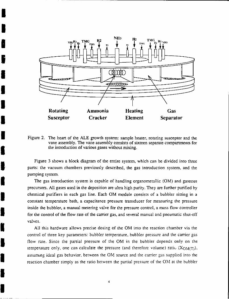
anticipated growth rate in the ALE mode is about I pm per hour. Figure 2 shows the heart of
the ALE system; i.e., the heater, the sample receiver and the vane assembly.
2

I0II
ii Load LockDiffusion
Pump
0 0
chamber
Growth Chamber
Figure 1. The top view of the ALE system showing all three chambers: load lock, cleaningchamber and growth chamber. The later two are visible also in the front view.33
NHI MG H2 N113 H2 TMG H2,H
Rotating Ammonia Heating GasSusceptor Cracker Element Separator
Figure 2. The heart of the ALE growth system: sample heater, rotating susceptor and thevane assembly. The vane assembly consists of sixteen separate compartments forthe introduction of various gases without mixing.
Figure 3 shows a block diagram of the entire system, which can be divided into threeparts: the vacuum chambers previously described, the gas introduction system, and the
pumping system.The gas introduction system is capable of handling organometallic (OM) and gaseous
precursors. All gases used in the deposition are ultra high purity. They are further purified by
chemical purifiers in each gas line. Each OM module consists of a bubbler sitting in a
constant temperature bath, a capacitance pressure transducer for measuring the pressure
inside the bubbler, a manual metering valve for the pressure control, a mass flow controller
for the control of the flow rate of the carrier gas, and several manual and pneumatic shut-offvalves.
All this hardware allows precise dosing of the OM into the reaction chamber via the
control of three key parameters: bubbler temperature, bubbler pressure and the carrier gas
flow rate. Since the partial pressure of the OM in the bubbler depends only on the
temperature only, one can calculate the pressure (and therefore volume) ratio (XOM(T)),
assuming ideal gas behavior, between the OM source and the carrier gas supplied into the
reaction chamber simply as the ratio between the partial pressure of the OM at the bubbler
4

II
Ip L -~ -
III C
0I0.)
I0)I -~0.)
-o
I -0.)
L.
I E
I0
IIIII
5
I

<=] Gas cylinder
IRegulator and cross-purge assembly
I Chemical gas purifier
Manual shut-off valve
Mass flow controller
Pneumatic shut-off valve
QCapacitance pressure gauge
K Manual mettering valve
Organometallic bubbler
3 W- Constant temperature bath
3 [ Automatic butterfly valve
Rotar> vane pui
II-IDiffusion pump
Ii[111111111] iScniber
IFigure 3a. Legend for Figure 3.6

Itemperature, POM(T), and the partial pressure of the carrier gas (= total pressure (pt)-poMMr).
XOMm =POM(T)Pt-POM(T)
The exact number of moles of OM introduced into chamber may then calculated from the
Iknown flow rate of the carrier gas.
The control of the introduction of the gaseous sources is much simpler: a mass flow
controller with a shut-off valve.
The pumping system consists of two diffusion pumps, one each for the cleaning and processchambers, and two rotary vane pumps. One of the latter serves as a backing pump for the
diffusion pumps and the other as the process pump. Both diffusion pumps are used to achieve
the ultimate pressure and to insure a clean process environment (i.e. a low pressure ofbackground contaminants) but are not used during the deposition. The volatile exhaust gasesare diluted with nitrogen and cleaned in a water scrubber prior to their release into a central
exhaust system.
Growth Theory. Several different precursors have been considered for the ALE of GaN.
After much study, organometallics were selected for the column III source-materials and
ammonia as the nitrogen source. Organometallic sources have been chosen over chloridesbecausc of their high purity, ease of transport from the source to the chamber and excellent
control over dosing. Triethyls were chosen over trimethyls for two reasons: (1) lower
decomposition temperature and thus lower growth temperature, which can potentially reduce
the concentration of nitrogen vacancies, and (2) cleaner surface reaction (trimethyls have
been known to leave high carbon residue at the higher deposition temperatures, which
become incorporated in the growing film). Ammonia has ben chosen over hydrazine and
nitrogen fluoride mainly because of safety considerations and cleanliness. Ammonia isavailable in research grade purity. Anmionia purifiers, which effectivly remove the
remaining water, oxygen and carbohydrides, are also available.
The reaction energy budget these precuisors offer theoretically favors the self-limitingI ALE deposition of HI-V nitrides on (0001) surfaces of the wurtzite or (111) surfaces of
zincblende substrates. The growth direction is crucial, because the number of bonds a
particular species makes on the surface varies greatly with the growth direction. A constituent
of a tetrahedrally bonded compound can make one surface bond in the 00- direction, two
surface bonds in (1011) direction and three surface bonds in the 0001 direction. The last two
cases are shown in Figures 4(a) & (b).
An estimate of whether a reaction is favored or not can be made by comparing the bondI energies of the reactants and the products. The bond energies between Group III metals and
nitrogen, calculated using different methods, are summarized in Table I.
II
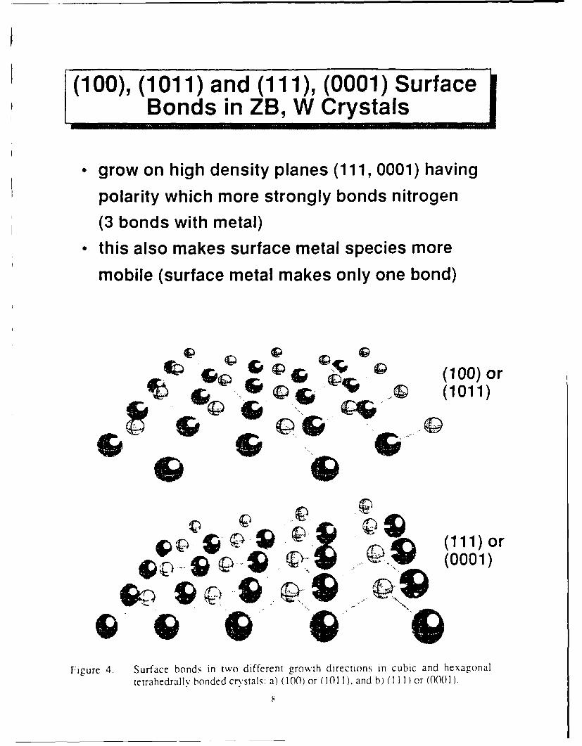
(100), (1011) and (111), (0001) SurfaceBonds in ZB, W Crystals !
0 grow on high density planes (111, 0001) having
polarity which more strongly bonds nitrogen
(3 bonds with metal)0 this also makes surface metal species more
mobile (surface metal makes only one bond)
OP CO(100) or
(1011)
(, ,)or(0001)
Figure 4. Surface bonds in two different growth directions in cubic and hexagonaltetrahedrallv bonded crstals: a) (100) or (1011), and b) ( 11]) or (000]).

Table I. Bond energies between Group II metals and nitrogen obtained by different methods.
B-N Al- N Ga-N In - N Remarks
93±5 71±23 87 * Tabulated values [5]
115 125 108 105 Pauling's formula [6]
94 90 65 54 Geometrical mean with correction [6]
83-193 52-122 55-85 47-67 Immediate neighbors
72-91 64-80 55-69 49-61 Periodic behavior
66 67(81) 50(56) 49 Heat of vaporization [7]
87 94 69 58 Heat of formation [8]
85±5 75±5 65±5 55±5 Suggested values
Suppose, the (0001) surface is saturated with the Ga(C2 H5)2 species, which make one
bond with the underlying nitrogen. When such a surface is exposed to ammonia, a reaction
will occur if making three bonds with Ga is energetically favorable for the nitrogen of the
ammonia molecule. The process will end with a hydrogen terminated surface, which does not
react further with ammonia. The bond energy between Ga and the ethyl radical is 57
kcal/mol, and the average bond energy between nitrogen and hydrogen is about 90 kcal/mol.
To make three new bond:- on the surface, one needs 3x57 + 2x90 - 351 kcal/mol. On the
other hand, production of one N-Ga bond releases 65 kcal/mol, and the reaction C2 H5 + H --
C2H 6 produces about 100 kcal/mol. Thus the total energy produced equals to: 3x65 +
2x10 = 395 kcal/mol. Since the energy produced is larger than the energy consumed, the
reaction is favorable.
A similar calculation can be done for the next, Ga layer. The Ga cycle starts with a
hydrogen terminated nitrogen surface. Arriving TEG chemically adsorbs on the surface by
breaking one H-N bond (90 kcal/mol) and one Ga-Ethyl bond (57 kcal/mol) and making one
Ga-N bond (65 kcal/mol) and one C-H bond (100 kcal/mol) producing C2H 6. The energy
balance is 147:165 and reaction is again favorable.
The same calculation is valid also for AIN and BN. The only III metal with a marginal
outcome is In, as can be seen from the data in Table 1. However, such calculations offer only
a rough estimate, since data on bond energies are not very accurate. Moreover, the change of
state from gas to solid has been neglected. Energy requirements on a surface which acts as a
catalyst may be even lower.
9

Growth and Analysis Procedures. In order to test and characterize the new equipment and
processes, several deposition runs were made using different growth parameters. Table II
gives the ranges in which the various parameters were varied. Throughout the test depositionsfour out of sixteen zones were used for TEG, four for ammonia and eight for the hydrogen
purge gas.
Table II. Growth parameters.
Growth temperature 350 - 6500 C
Growth pressure 0.5 - 50 TorrAmmonia flow rate 100 - 300 sccmH2 (purge) flow rate 200 - 300 sccm
H2(OM carrier) flow rate 50 - 100 sccm
TEGa bubbler temperature -10 - 200CTEGa bubbler pressure 400 - 800 Torr
Rotation speed 1- 2 RPM
Reflectron High Energy Electron Diffraction (RHEED) was performed on the grown
films to determine the crystallinity and structure. Scanning Auger microscopy (JEOL JAMP-
30) was performed to determine the presence of impurities and nominal composition of theGaN layers. Scanning electron microscopy (Hitachi S-530) was performed to evaluate the
surface morphology of the deposited thin films.
C. Experimental Results and Discussion
Surface Morphology. Initially, a few. CVD runs were attempted, where all reactants were
introduced into the same growth zone. The substrate temperatures were rather high, 750-
850'C, and the process routes did not result in the growth of any GaN films. Only large
(>10 gim) individual GaN crystals were observed on the surface, as shown in Figures 5(a) &
(b). They are a possible result of homogeneous nucleation in the gas phase.
After a few unsuccessful experiments, the reactants were separated and distributed to
different growth zones. The substrates were rotated and sequentially exposed to different
reactants. Films were grown at constant chamber pressure of 50 torr, while other parameters
such as, growth temperature, flow rates, and the rotation speed were changed.
10

-SA
44
\U1II V ~ \Ii"lm1 t1 o(l cciII1 l clP I11C\ , , IC

I
Figures 6, 7 and 8 show the surface morphology of three GaN films grown under
different conditions. Figures 6(a) & (b) shows a film grown at 560C. Note the much higher
nucleation density than in Figure 5. Figure 6(b) has been taken close to an edge of the wafer,where the nucleation density was low, and the individual crystallites were clearly seen. All of
them have either a hexagonal or a triangular shape, both of which indicate a hexagonal
structure. All of them are also oriented in the same direction; note, that all {0001) planes are
perpendicular to the surface and { 1010) planes of the individual crystallites are parallel
among each other. This indicates a good epitaxial relationship with the ct(6H)-SiC (0001)
substrate.
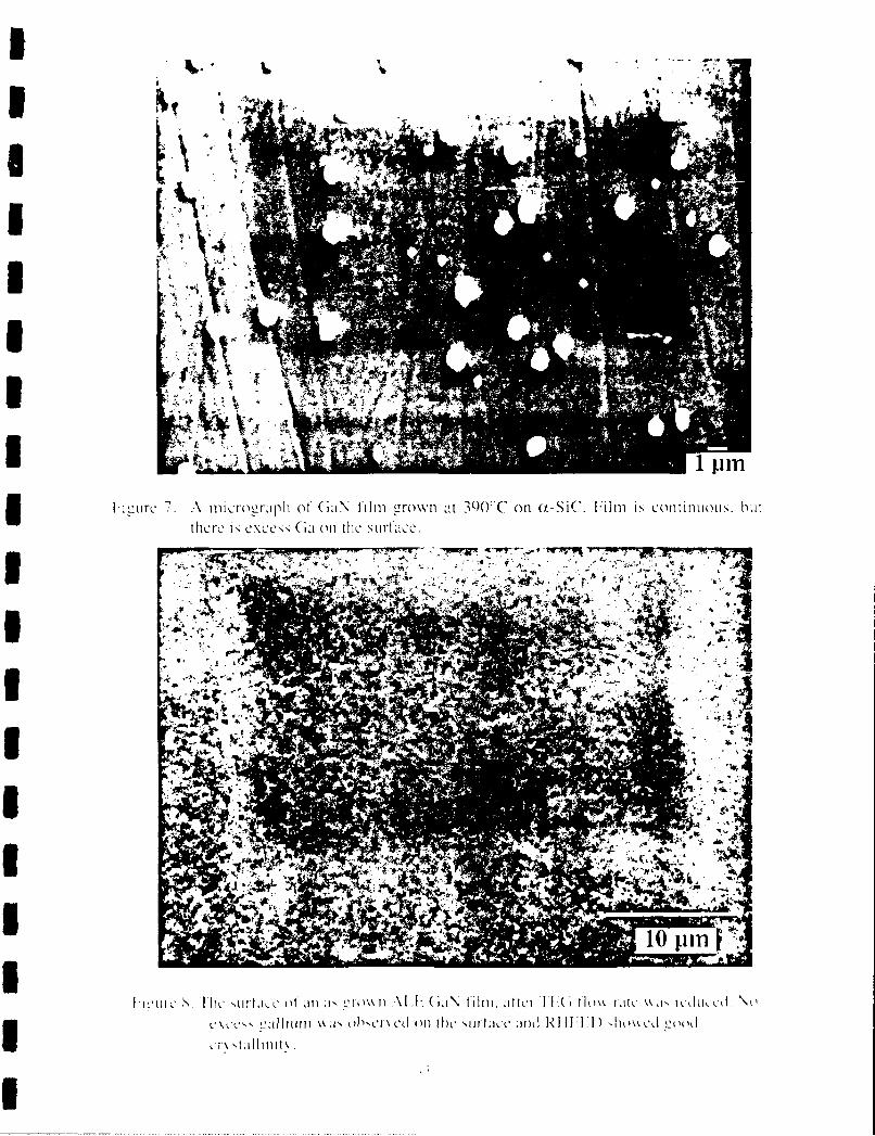
Figure 7 shows the surface of a GaN film grown at 3900 C. The film is continuous, as
confirmed by chemical analysis. The ovals on the surface of the film are conglomerates of
unreacted gallium. Apparently TEG decomposes at this temperature effectively; however, the
concentration of ammonia is insufficient for complete reaction. When the supply of TEG was
reduced by about three times, a clean GaN film without Ga precipitates was obtained, as
shown in Figure 8. However, this procedure also reduced the growth rate from 2000 A/hr to
600 A/hr.
Chemical Analysis. Scanning Auger microscopy was performed on the samples to
determine the presence of impurities and the nominal composition of the GaN layers.
Figure 9 shows an Auger spectrum taken from the untreated growth surface. The oxygen and
carbon peaks are due to surface oxidation and contamination upon exposure to the
atmosphere. No other contaminants were observed to the resolution of the instrument
(typically =0.1 at.%).
An Auger depth profile was also obtained and is shown in Figure 10. The profile shows
that indeed the oxygen and carbon contamination was only on the surface. The apparent low
nitrogen content of the film is in part due to the relative elemental sensitivity factors. Another
factor may possibly be a result of the sputtering action of the 3 kV Ar+ ions. A similar effect
has been seen in InN 9.
Electron Diffraction. Reflection high-energy electron diffraction (RHEED) was per-
formed on GaN films. Films grown at 350'C and lower showed only a diffused ring
diffraction pattern and were apparently amorphous. Films grown at 380C or higher showed a
distinct diffraction pattern indicative of the wurtzite structure. Diffraction patterns of a film
grown at 390'C and taken in two different directions are shown in Figure 11. Although
Kikuchi lines were observed which are the fingerprint of good crystallinity, the surface of the
film appears to be rough, as shown by the spotty diffraction pattern.
12

OP
'*#Ab'
Li. '~p~m-%~~Q
Il
It ufc lopo(L\o W i tSC i)%1 l 0 .N I t11II mdeIIIIit~ ld l~1 hl l lnr .IlA 11r urp a elilfi d' ftl 'liIIc- kh r ien ce to clI\\%I m oc11 C-c Io"clalnl*ealwhpIc~c r 1(1\I~ l r I11IN
1a t
II 7
I (11 l)"lC IIh'N Vt - 1lL Mc L(10

-2000
U 501000 1500 2000KDNETC EDY (GY)
I Figure 9. Auger spectrum taken from the untreated GaN surface. Only oxygen and carboncontamination was detected, which is due to exposure to the atmosphere.
70-
a.aIN
Cjj 30)
2o-
.... .. . . .. .. . .. .. ... ... ... ...
I I
5 Spuiicnng Timec Imii
Figure 10. Auger depth profile of GaN on ax-SiC (0001). Oxygen and carbon contaminationwas detected only at the surface.
15

IIUIII1IIIIIIIIII
I ] III I I) ~~!l~ri~ I ( i~N Ii III I~\ \I I (
II,

D. Conclusions
The initial results of the ALE growth of GaN are very encouraging. The system has been
performing i". a satisfactory manner. Although the growth results are improving from run to
run, the self-limiting ALE growth regime has not yet been achieved.
Apparently ammonia does not react very efficiently at the present growth temperatures.
To promote the reaction, tungsten cracker filaments were installed in each ammonia zone.
These filaments will run at 800-1200'C which is much higher than the substrate temperature
and should greatly enhance the reactivity of ammonia.
E. Future Research
The research on the ALE of GaN will be continued. A similar process for AIN and their
solid solutions and heterostructures will also be determined and employed. The conditions for
a self limiting process in the growth of all III-V nitrides will be investigated. The
effectiveness of the ammonia decomposition in the cracker filaments on the low temperature
(:350'C) deposition of stoichiometric GaN and AIN will also be determined.
H. GROWTH OF CUBIC BORON NITRIDE
A. Introduction
Boron nitride has long been known for its desirable properties as a highly insulating as
well as a chemically and thermally stable material. Thin films of cubic boron nitride (C-BN)
have many potential applications in areas such as diamond substrates and optoelectronic
devices in the vacuum ultraviolet. The cubic phase was first reported by Wentorf,[10] who3 produced it in a high pressure apparatus and even made the initial measurements on the
material's semiconducting properties. It has been used since then primarily for its high3 hardness in applications such as grinding and polishing. The cubic phase of BN is actually2the zinc blende structure or in space group notation F43m (Hermann-Mauguin) or T d
I (Schbenflies). Boron nitride is very similar to carbon in that both exist in hexagonal,
wurtzitic, and cubic forms and many of the properties in each of the phases are strikingly
similar. The rare exception is that hexagonal boron nitride is an insulator and hexa-gonal
carbon is a conductor. Among the many similarities include the fact that both diamond and c-
BN are metastable under the conditions currently used for growth of thin films.
Interest in the cubic polymorph of BN as a semiconductor material has received much
interest recently as a possible substrate for the deposition of diamond, due to the similar lat-
I tice parameters (Aa&=.34%) and its wider bandgap which is in the range of 5.8-6.5 eV.[ 11-
13] The very wide bandgap of c-BN also gives c-BN applications in its own right, as optical3 devices for the vacuum UV (X-200 nm). For a complete listing of materials-related properties
17

of c-BN see Landolt-B6rnstein:Numerical Data and Functional Relationships in Science and
Technology, Series III, Vols. 17 and 23, or Ref. [14] (which also includes a side-by-side
comparison of properties of c-BN with diamond).
Several approaches have been employed in the attempt to grow thin films of cubic boron
nitride (c-BN). These include reactive diode[15] and rf sputtering,[16] ion implantation,[17,18] plasma CVD,[19-21] microwave plasma CVD,[22, 23] and ion plating techniques.J24-
27] These attempts were successful in producing polycrystalline films of c-BN, pre-
dominantly of a mixed nature with both cubic and other phases present and of extremely fine
grain size. It appears that most researchers succeeded in the deposition of c-BN if the
technique included the input of additional energy from energetic ions during the deposition
process.
B. Selection of Substrate Materials, Deposition Technologies and Analytical TechniquesStz:bstrate Materials. In the present study, film growth has been attempted primarily on
single crystals of silicon and copper. Silicon was chosen since it is well characterized and
understood, readily available in single crystal form, and nearly all previous studies have
included silicon as a substrate. Additionally, it is a technologically important material forheteroepitaxy of c-BN in microelectronic applications. There is also some evidence that
indicates that despite the high lattice mismatch of c-BN--Si (=33%), a much lower strain
(=4%) atomic coincidence boundary does occur,[28] which might permit high quality layersto be produced with Si as a substrate.
Copper was chosen primarily because of its near perfect lattice match (Aa 0=0.022%). The
thermal expansion difference is slight (=10 ppm/°C) and actually improves the lattice match
at gro':.'th temperatures. Copper does form a nitride (Cu3N) which could pose a problem at
the growth interface, but it decomposes above 300-400'C,[29] and its lattice parameter
(3.815 A)[30] is only =5% larger than c-BN. Since growths have taken place at highertemperatures (500-700'C), formation of an interfacial phase which might interfere with the
growing layer is not expected. Surface energy difference is a problem, as copper has a much
lower surface energy than c-BN (1430 vs. 4770 erg/cm 2).[14, 31] This problem plagues c-BN
heteroepitaxial deposition in every case except c-BN on diamond. This problem will be
discussed further in the section on Future Research.
Deposition Technologies. Gas source molecular beam epitaxy (GSMBE) was chosen for
several reasons. The UHV conditions of the system provided very clean background
conditions for growth. Many if not all of the films grown in previous studies contained
oxygen in the films and contamination is a serious problem for electronic materials. The in
situ capability of RHEED as well as the additional in vacuum analytical techniques of LEED
18

I
and XPS, permit careful evaluation of the film before degradation upon exposure to the
atmosphere.
The compact ECR source (described briefly in the Experimental Procedure and in detailin Ref. [32]) produces excited as well as ground state species within the intense plasma
I conditions of the source. The presence of these excited species is important to the formationof the metastable cubic phase. Since the difference in enthalpy of formation between the
I hexagonal and cubic phases is small (=3.63 kcal/mol @ 25'C), the primary problem is a very
high activation barrier between the phases. Use of these excited state species is important to
overcoming this barrier. However, very high kinetic energy species are not desired as they
will produce many defects in the growing layer. This problem will be discussed further in the
section on Ft.tre Research.
Microwave plasma CVD was also investigated as a potential method of depositing c-BNfilms since some investigators had used it successfully in producing partially c-BN films and
might be successfully extended to single crystal films. An agreement was reached with
ASTeX, Inc., in Boston, MA, whereby one of their microwave plasma CVD systems was
I adapted for BN deposition. This involved installing a new mass flow controller and a bottle
of borazine liquid into the gas handling system. For the depositions, M. J. Paisley went to
ASTeX, Inc., and worked with Mr. Larry Bourget of ASTeX in setting process parameters
and performing the depositions.Analytical Techniques. XPS, RHEED, and LEED are iz vacuo techniques for the MBE
system and thus are natural choices for films grown in that system. RHEED (for review of the
use of RHEED see Ref. [33]) and LEED (described in detail in Ref. [34]) are very sensitive
techniques for determining crystal structures and can also give information regarding certain
details of surface morphology. XPS gives information regarding chemical purity and some
information regarding chemical state of constituent species. This is not particularly true for
nitrogen, as its electronegativity (only oxygen, chlorine and fluorine are higher) results in
only very minor shifts in peak position as a function of stoichiometry.[35] XPS can
potentially also give structural information through the plasmon loss features associated with
the elemental peaks.[36]
X-ray diffraction and TEM also give very good structural information, x-ray diffraction
on a much broader scale than RHEED and LEED, while TEM is on a much finer scale of
structure. In addition, TEM and SEM give detailed structural and morphological information
on the films and substrates.
Additional purity and local structure information can be obtained from transmission FT-
IR measurements. The infrared region corresponds to excitation of phonon modes in the
material for bond stretching and bond bending processes.[37] These energies are unique for
each type of bond, so that B-N bond stretching can be differentiated from B-H bond
19

I
Istretching, etc. This differentiation allows FT-IR to determine presence of contaminants in
general, and an ability to detect hydrogen, which is difficult by most analytical methods.
Since some of these bond excitation processes are three-dimensional in nature and arerestricted in their degrees of freedom by the surrounding crystal lattice, FT-IR also provides
Ilocal structural information which can indicate the structure of the surrounding lattice.[38]Silicon is an excellent substrate material for FT-IR measurements since it is transparent inI the infrared region scanned (400-4800 cm- 1, 0.05-0.6 eV, X=25-2 I.tm). For these reasons,
transmission FT-IR has been used by many researchers[21, 22, 27, 39-42] as a non-
destructive technique for observing the cubic and hexagonal or amorphous phases of
deposited BN films.
Raman spectroscopy excites the same phonon modes in the material as infraredspectroscopy though via different processes. Whether a phonon mode is infrared or Ramanactive (or both or neither) is dependent upon whether or not creating (or destroying) thatIphonon would change the dipole moment or electronic polarizability, respectively, of thecrystal. Since the lattice site symmetry of the molecule is different in different crystalIstructures, Raman and/or infrared spectroscopy can be used to determine crystal struc-tures.[37, 38] This can be critical in cases of single crystal films as certain phonon modes can
be suppressed when analyzing samples in specific orientations. [43]
C. Experimental Procedures
Gas Source MBE. The primary deposition technique was GSMBE wherein elementalboron is evaporated from a high temperature effusion cell and molecular nitrogen gas ispassed through a compact electron cyclotron resonance (ECR) plasma source to activate and
dissociate the nitrogen. The growth system was a Perkin-Elmer 430 MBE system modified as
described below. It consisted of three major sections: a load lock (base pressureI =5 x 10⁻⁸ Torr), a transfer tube (base pressure =3 x 10⁻¹⁰ Torr) which was used to degas the
substrates, and the growth chamber (base pressure =1 x 10⁻¹⁰ Torr). The growth chamber was
equipped with four standard 20 cc effusion cells that contained BN crucibles which were
resistively heated with Ta wire heaters used in research of other nitrides.
One modification was the addition of a special high temperature effusion cell. This cell
uses a W3%Re-W26%Re thermocouple and a tungsten alloy heater filament which is driven
by a 2700 W DC power supply. It mounts on a standard 4.5" metal seal flange along with allthe other metal evaporation sources. A BN crucible was used as it was believed that slight
decomposition of the crucible at the elevated operating temperatures would not affect the
growth of BN films. Prior to installation of the source, the BN crucible was loaded with 3 g
of 99.9999% pure boron.
20

The more significant modification was the use of a compact ECR microwave glow-
discharge plasma to dissociate/activate the N containing gas. This source was designed and
commissioned in an in-house effort by Dr. Zlatko Sitar.[32] This source has the advantages
of fitting inside the nominal two-inch diameter tube of the source flange cryoshroud and thus
minimize the source to substrate distance. As a result, the flux of activated/dissociated
species arriving at the substrate surface is increased. This source was attached in place of a
more traditional effusion (or cracker) cell for the group V element. The nitrogen gas was
taken from a bottle of compressed UHP-grade nitrogen, purified by a metallorganic resin bed
gettering material and subsequently regulated to the source by a variable leak valve.
Some depositions also included use of borazine (B3N3H6 ) in a nitrogen carrier gas as
both a source for boron and for nitrogen. Borazine was chosen as a gas source for boron to
investigate activation of the source of boron in the ECR plasma as well as an attempt to
determine if boron-nitrogen compounds provide a more suitable precursor since the B-N
bond already exists in the material. This was done by placing the borazine (which is liquid at
STP) in a temperature controlled bubbler and passing nitrogen gas through it which then
passed into the ECR source.
Substrate preparation involved a 30 min. exposure to UV which has been shown to
remove hydrocarbon contamination,[44] followed by a dilute acid etch to rcmove oxide
layers. In the case of Si, a solution of H20:HF (10:1) was used,[45] and for Cu, a solution of
H20:HCl (10:1) was used.[46] Subsequently, the substrates were mounted on a Mo holder
using either molten indium or silver paste. Silver paste was very important for the copper
substrates as they were extremely sensitive to oxidation and would oxidize heavily in
attempting to indium bond the substrates.Samples were then loaded into a cryopumped load lock. After the initial evacuation, the
samples were loaded into the transfer tube where they were degassed to a temperature of
7001C. Immediately after degassing they were loaded into the growth chamber and the
deposition cycle began. Typical deposition conditions used are shown in Table I.
Table I. Deposition Conditions used in GSMBE of BN
Nitrogen pressure 1-2x 10⁻⁴ TorrMicrowave power 20-50 WBoron temperature 1725 - 1775 0CBorazine temperature (where used) -10 0 CSubstrate temperature 600- 7000 CGrowth time (BN) 120 - 360 min.Deposited film thickness 10-850 A
21

Subsequent to deposition the sample would either be moved to the load lock for removal
from the system or transferred to the analytical system for additional characterization.
Microwave Plasma CVD. The microwave plasma CVD system consisted of a gas
manifold where gases could be injected directly into the plasma or downstream from it.Depositions were performed in two modes: (1) borazine, nitrogen and argon were introduced
in the plasma, and (2) argon and nitrogen were injected into the plasma and the borazine wasinjected downstream. The substrate support was isolated making it possible to add rf biasing
to the substrate to increase ion bombardment from the plasma. A schematic diagram of the
ASTeX system is shown in Figure 12.Substrates of Si (100) or Si (111) along with quartz and tool steel were placed into a load
lock and evacuated before loading into the main deposition chamber. Then the samples were
heated under vacuum until the deposition temperature was reached. Finally, gas flow was
begun and the plasma was ignited and deposition commenced. In situations where substrate
bias was used, the plasma was initiated and stabilized then the bias conditions established and
finally deposition began. After deposition, the samples were cooled and removed forellipsometry and eventual further analysis at NCSU. The range of conditions used for
deposition is shown in Table II.
Table 1I. Deposition Conditions used in MWCVD of BN
Borazine flow 1.5 - 10 sccmNitrogen flow 0- 20 sccmArgon flow 0- 50 sccmChamber pressure 0.9 - 5.0 mTorrMicrowave power 500 - 1000 WSubstrate temperature 590 -620°CSubstrate rf-induced voltage 0 to -65 VGrowth time (BN) 3 - 30 min.Deposited film thickness 50 - 2000 nm
Some readers might be confused by the entry for Suh.strate rf bia voltage listed in
Table I1. When the f bias was applied to the substrate, the presence of the plasma caused a
DC bias to be induced on the substratc surface. T,,,, bias resulted in ions being accelerated to
the substrate surface. This induced bias is a much more descriptive measure of the effects of
the rf biasing than the measure of f bias power applied, and thus is used instead of the
power. (Note: This rf bias was measured simply by attaching a voltmeter between ground a
the substrate holder with the addition of a lob -pass filter to protect the voltmeter from rf
voltages.)

Symmetric Microwave Components
Plasma Coupler4W Source
ECR Source
Gas Injection
.o- Window Magnet
ECR Sourcec-e-
Downstream "Gas Injection [- Exit Magnet
LoadlockTurbo Pump Gt av
50 cfmbacking pump - Induction Heater
Figure 12. Schematic diagram of microwave plasma CVD system used at ASTeX, Inc. todeposit BN films.
23

D. Results
Gas Source MBEBN on Silicon (100) Substrates. The BN films grown on silicon substrates exhibited very
good chemical purity but poor crystal structure definition as was shown in the previous
progress report of December, 1990. Only nev and additional results will be reported here.
Infrared spectroscopy (FT-IR) can be used to give further chemical and structural
information on the deposited layer. Arrangements were made to perform FT-IR mer sure-
ments in the Textile Engineering, Chemistry, and Science Department here at NCSU. Shown
in Figure 13 is an FT-IR spectra showing absorption features of the BN film after background
subtraction for the Si substrate and atmospheric absorption effects.
IBN on Si (100)ITransmission FT-IRResolution: 4 cm -1 CO2Nicolet 510P
P,-BN c-BN a-BN
I
4500 4000 3500 3000 2500 2(, 1500 1000 500Wavenumber (cm )
Figure 13. Transmission FT-IR spectra of BN deposited on Si (100) substrate. Inverted C02absorption peak is present because concentration was lower when analyzingsample than for instrument baseline spectrum.
Copper Substrates. Analyses of the initial copper substrates (99.999% pure) were
undertaken to determine the initial purity of the substrate surface as well as its surface
structure. Figure 14 shows the Auger electron spectrum of the substrate surface after 700'Cvacuum anneal. Note that no oxygen and only a trace of carbon are observed, indicative of
good substrate preparation prior to evacuation. The sulfur peak and some of the copper peaks
appear as doublets indicating that the sulfur is present in two different states. There is no
24

chlorine present which is observed in HCl-etched copper,[46] probably due to removal of the
chlorine from the surface in the vacuum annealing stage.
Cuu Cma C
SL
JAuger Electron Spectra
Cu (110) substrate700°C anneal
CU NJ 1 eV resolution
100 200 300 400 500 600 700 800 900 1000Electron Energy (eV)
Figure 14. Auger electron spectrum of Cu(l 10) substrate. Note presence of sulfur (doublet)and trace of carbon contamination.
To determine the degree of surface order, LEED patterns were taken at several differentvoltages. Shown in Figures 15 and 16 are two of the LEED patterns observed from the
Cu(1 10) surface. Note that several fractional order beams are observed clearly in Figure 15and this pattern is tentatively assigned (1 xi ) with additional spot splitting.
This is more clearly observed in Figure 16, where a more complete but more diffuse
pattern is observed. The more complete pattern is due just to the decrease in electron
wavelength as the electron energy is increased.
High resolution field emission SEM (Hitachi S-4000) photographs were taken to
determine the quality of the initial growth surface of the Cu substrates. Figure 17 shows both
low and high magnification images from the substrate surface. The relatively smooth surface
is apparent, except for occasional scratches and a very fine texturing observable only at high
magnification. Some small dimples were also observed in the surface from the
electrochemical polishing step (not shown) which were widely separated.
25

IIII I ( )
I*
II
13. I IKIKI ) ;'ut:c~n oD~c1\ H cm Cu I 1W stjh>trwc lx'w:c ~Ux\::.cm .v.: 2 I (.iflfl&.:I '1B)X\ :1: 122 1~I'2. 1 19, JXKi~2 \\it1~ :1 9\\ !&'(':2'~Y::c1:' Urn K>
IIUIIII
II

(a) (b)
Figure 17. High resolution SEM photograph of Cu (110) surface: (a) low magnificationimage with (Tray pattern of low levels of hydrocarbon contamination but smoothsurface, and (b) higher magnification showing very fine texturing of surface.
B.\ on Copp er SUbstrates. After deposition of the BN films, the samples were reanalvzed
by XPS and LEED to determine their purity and surface structure. Figure 18 show the XPS
results for the BN on Cu (I110). Note that there is no contamination apparent and that the
copper peaks are qui.1te strong. Standard sensitivity factors[47] show that copper is not present
in the ratio that appears in the figure. Whille these sensitivity factors do not necessarily' apply
for the spectrometer used, the sensitivities would not likely vary dramatically.
RtHEED performed after the growth showed a diffuse CuI (110) pattern indicating2
crystalline growth. LEED results after deposition showed that the reconstruction spots had
disappeared but the baIsic [I 1101 pattern remained as can be seen in FiguLre 19. The pattern also
11,P, ZI 11LCh1 higher background intensity than before deposition..%t highier beami energies, streaking i the I1](11 direction is ipaen s shown i
:iLII'V 2(0. This streaking indicates formation of sniall facets or steps .1 341
.\trrenloval froin the chaniber, sam11ple surfaces were again observed in a high
IrC,,0,0tlt 1 hield cm iso SEM . Ih BN s ra eiss o ni -g r 1
S:iniples % crc also examined with R,111,1T spectroscopy (in the lihoratory of' Robert
Ncmtnih>.There % Crc no o, ,cr\ahlc pc~ik , in the specra,. i.c., no pecaks froni either-, Or- CIiC p f 01' ni triC.
I2

Cu2 /2XPS-Mg anode
Resolution: 1 eVCu (110) substrate
Cu2 h,,
4 Cu ,v Cuw
BlS Cu,. Cuhp
1000 900 800 700 600 500 400 300 200 100 0Binding Energy (eV)
Figure 18. XPS spectrum of BN deposit on Cu(1 10) substrate. Cu-2p3/2 sensitivity is -50xgreater than that of B-I1s and -10x greater than N- 1 s.
[001]
I$
Figure 19. LEED patterns observed on BN deposited on a Cu (I110) substrate showing basic(110) pattern (Beam=95.0 V).
28

,I~
~~~I vncr .. ii ) It sta, i ntll t)h'C 1 101 BN JcpOt~on (uctm I 1 V ':1 h\1> iC
\\ ~ ~ ~ ~ ~ ~ ~ ~ ~ ~ ~ ~ ~~A iti-1 k nteI11) ~i~1f ct 77.
I ;; ~ ~ ' 20

I
U Microwave Plasma CVD. After removal from the system the films were analyzed using a
rotating polarizer type ellipsometer. This gave index of refraction results for the grown films
and the resulting index varied over the range of 1.65-2.28 (c-BN n=2.12) An x-ray spectrumis shown in Figure 22, where the measured index was 2.01.
i Si S BNonSi(11)(11() (222) (33) 1000 W iWaveI5 sccn borazine
20 sccm nitrogen10 sccm argonX-ray: CuK
(111)" CuKI
BNre on
I20 30 40 50 60 70 80 90 100 110 1200
Diffraction Angle (2 8)
Figure 22. Typical x-ray spectrum from BN deposited in ASTeX microwave CVD system.Note BN region which cannot be resolved into individual peaks present.
FT-IR spectra of this film shows both hexagonal and cubic BN phases present along withvery minor amounts of hydrogen incorporation under some processing conditions as is shown
in Figures 23 and 24.
Compare that spectrum with Figure 24 which shows spectra from several different
deposition conditions. Note the variation in intensity of the N-H stretch and 3240 cm- 1 peaks
as well as both peaks for h-BN.
As a companion technique to the FT-IR, samples were analyzed with Raman
spectroscopy. Figure 25 shows a spectrum from the best conditions film showing a mix of
phases.
Next cross-section TEM samples of the apparent best condition (1000 W, 10 sccm Ar,
0 V bias) were prepared using standard techniques.[48] Shown in Figure 26 is a bright field
image (z=[l 101) of the BN film with the SAD pattern in the inset. Not shown in this figure,
30

BNon Si (111)Borazine downstreamnI Nicolet SlOP FT-IRScans avg'd: 32 .1 N-H C2h-BN h-BNResolution: 4 cm jstretch CO2 N
323I 615
I ~~ ~ 9 1 1 g ~I I 4 a I I gI a I I I I I gI I* II *
4500 4000 3500 3000 2500 -)2000 1500 1000 500Wavenumber (cm 1
Figure 23. FT-LR spectra of BN on Si(1 11) showing h-RN and c-RN peaks and very littlehydrogen/argon incorporation (Ar flow= 10 sccm, 1000 W, 0 V bias).
I 3242
0)0
- 2Vba,5scnA,10W
-20 V bias, 50 sccmn Ar, 100WCO-5Vbias, 1 cmAr, 1000 W
0 .V bias,10 sccm Ar, 1500 WI~~ ~~ . . I I I . I I I I . a I . I . I I I- I I I I I I . . 9 1
4500 4000 3500 3000 2500 .12000 1500 1000 500Wavenumbcr (cm 1)
IFiszure 24. FT-IR spectra of BN on Si (Ill1) under various processing conditions showingheavily distorted h-BN and c-BN (almost invisible) pc~aks and showing stronghydrogen/argon incorporation.
31

I CTrS/SEC XIE3
1. 600-
1.400
1.200 T10.1 1.000
1000.0 110.0 1200.0 1300.014.RC?4-i
IFigure 25. Raman spectrum of BN on Si (111). Shows presence of peak from h-BN(1371cm- 1 ), c-BN (1295 cm-1 ), and unknown peak (1244 cm-1). The offscaleI peak at = 1120 cm-1 is due to overhead lights and should be ignored.
IleLn
ISi substr at .J.0.-P
Figure 26. XTEM photograph of BN on S I (I111) with z=[ 1101. Inset shows SAD pattern ofSi with oriented polycrystalline h-BN.
32

but observed were areas of amorphous nature as well. The film is measured to be 0.7 Am
thick which corresponds to a 1.4 gm/hr growth rate.
Samples grown at high substrate bias condition (50 V) delaminated from the Si
substrate. Pieces of the delaminated films were placed on nickel grids and examined in the
TEM. Figure 27 shows an SAD patterns from a typical region of the BN layer.
Figure 27. SAD pattern typical of BN layers showing diffuse rings indicative of amorphousnature with some sharper rings showing hexagonal structure.
E. Discussion
Gas Source MBE
BN on Silicon (100) Subs trates. The FT-IR spectra shown in Figure 13 indicates the
presence of a-BN and c-BN. The peaks labeled a-BN are in the same location as seen for h-
BN. This points to a minor problem in that the infrared absorption spectra cannot seemingly
differentiate between amorphous BN (a-BN) and h-BN. For example, Ikeda et a1124] reported
IR peaks for a-BN in the same location as they occur for h-BN.[49] This is because while the
c-BN peak is due to a three dimensional process (transverse optical or TO) phionon while the
h-BN peaks are due to B-N stretching and B-N-B bending, which are lower-dimensional
I processes. We sug7gest that these lower-diniensional processes are perhaps not sufficiently
sensitive to long range order to differentiate between arnorphOLus and hexagonal phases. ThuIsI
I 3

the assignment of these peaks as a-BN rather than h-BN is based on x-ray and TEM
diffraction data as well, and not just FT-IR information alone.
Copper Substrates. The initial state of the growth state is important to the formation ofhigh quality deposited films. It may be even more critical in the case of c-BN, as the cubic
periodicity of the substrate surface may help induce the metastable formation of c-BN.The initial substrates were found to have significant levels sulfur contamination as was
shown in Figure 14. The source of sulfur is unclear at present, but a common electrochemical
etching solution (used after mechanical polishing) is mercapto-sulfur based,[46] and thus is a
likely candidate source of the sulfur. This sulfur would most likely appear as Cu2 S (m.p.
=I 100'C), since sulfur has a low boiling point (--450°C) and would have been removed by
the anneal. The split peak in the sulfur Auger spectrum of Figure 14 may indicate presence
two types of sulfide, but by itself, is not sufficient evidence to determine the states of sulfur
on the copper surface.Clean Cu (110) surfaces have a simple (1 xi) structure,[20] whereas sulfur adsorbed on
Cu (110) induces several different surface reconstructions, depending on the amount of
coverage. Boulliard and Sotto[50] reported that Domange had determined the saturation
coverage of sulfur on Cu (110) to be 0.64. Boulliard and Sotto found that sulfur induced
numerous reconstructions changing with increasing normalized fraction of the saturation
level (0). At near saturation levels (0.7 0<1.0), they observed (1/2,1/2) doublets in the [110]
direction. They also observed as coverage increased, the separation of the doublets increaseduntil it became a c(8x2) structure. They also mention that at or near saturation, othersobserved a c(2x3) structure.
Figures 15 and 16 together show indications of the widely separated (1/2,1/2) doublets in
the [110] direction, indicating a near saturation coverage of sulfur. In addition the spots are
diffuse which may indicate disorder in the sulfur surface, which may explain the splitting
observed in the sulfur Auger peak.
It has been reported by Yarmoff and Williams[51] that a LEED pattern with small spot
size and low background intensity does not necessarily reflect a well-ordered surface in
copper. However, their annealing steps were at a homologous temperature of only 0.43 Tm,
while these substrates were annealed at 0.59 Tm. So it is expected that the copper near-
surface region is at the very least, approaching a well-ordered condition and the diffuse spots
are from disorder in the sulfur coverage, rather than disorder in the underlying copper lattice.
BN on Coyner Substrates. The XPS spectrum in Figure 18 showed that that the sulfur and
trace carbon are now completely gone and only copper, boron, and nitrogen remain. Note that
the copper was still very much in evidence after deposition of a film which should have been
-500 A thick. Given the surface sensitivity of the technique, this thickness would very
34

thoroughly eliminate the copper peaks from the spectrum. The large difference in elemental
sensitivities shows that the substrate is covered more completely than it first appears, but
does not explain why the copper peaks are still present.
This is most likely due to island formation which occurs when the surface energy of the
adlayer is higher than that of the substrate. As was discussed in the Introduction, the surface
energy of c-BN is over four times as much as that of copper (1430 vs. 4770 erg/cm 2).[14, 31]
This large difference is a strong driving force for the formation of islands on the surface
rather than the smooth film desired. Island formation is also indicated by the LEED
photographs shown in Figures 19 and 20. The basic Cu (110) pattern is still evident in
Figure 19 though more diffuse and Figure 20 shows that the [110] spot splitting has becomesimple streaking along the same direction. These streaks are usually attributed to formation ofdirectional steps or facets along the surface.
The idea of island formation is confirmed after examination of the surface with a high
resolution SEM as was shown in Figure 2 1(a) and (b). Islands are clearly visible in both
micrographs with a rectangular structure evident in Figure 21(b). The Raman spectra from
these samples gave no evidence of either cubic or hexagonal structure. This may be due to
being amorphous or to being microcrystalline as Ikeda et al have attributed to their films.[27]
It should be emphasized that due to the strong island formation observed, that the RHEED
and LEED results cannot be used as indicator as to the crystalline nature of the BN deposit,and will thus require further analysis to determine the structure.
Microwave Plasma CVD. The x-ray diffraction spectrum in Figure 22 shows only a broadband of reflections in the region of 42-50' 20, v as .,i,i ,,.. lv ih, from Table III covers a
number of peaks from all phases of BN. The Si (111) Cu Kp3 peak is exactly where predicted,
but is somewhat unlikely since the detector has a graphite monochromator to reduce that
peak. The h-BN (002) peak is either obscured in the lower edge of Si (111) peak, or has
shifted down slightly and is where the Cu KO peak should be. If this were the case, its relative
intensity would seem to indicate a significant portion of the broad BN region is from phases
other than h-BN. The fact that the region is continuous also indicates at least some
amorphous component.
The FT-IR spectrum shown in Figure 23 shows a fairly clean spectrum with only very
slight hydrogen/argon incorporation as indicated by the almost undetectable peaks in the
3200-3500 cm - 1 range. The peak at 615 cm - 1 has not been identified and only occurred in
this spectrum while the peak at 3230 cm - 1 is apparently related to incorporation as will be
discussed next.
35

Table m. Diffraction peaks for phases of BN using Cu Kx radiation.(Source: JCPDS card file on CD-ROM)
Crystal Phase Relative Intensity Crystal Plane Diffraction Angleh-BN 100 002 26.80
w-BN 100 100 40.80h-BN 15 100 41.60
w-BN 70 002 42.70c-BN 100 111 43.30h-BN 6 101 43.90
w-BN 45 101 46.30h-BN 9 102 50.10c-BN 5 200 50.40h-BN 6 004 55.20h-BN <1 103 59.60
w-BN 18 102 60.60w-BN 45 101 46.30h-BN 9 102 50.10c-BN 5 200 50.40h-BN 6 004 55.20h-BN <1 103 59.60
w-BN 18 102 60.50h-BN 2 104 71.40c-BN 24 220 74.10
w-BN 25 110 74.20h-BN 5 110 75.90
w-BN 16 103 80.80h-BN 5 112 82.20h-BN <1 105 85.50h-BN <1 006 87.90
w-BN 12 112 89.60c-BN 8 311 89.90h-BN <1 200 90.50h-BN 1 202 96.70h-BN 3 114 100.70h-BN <1 106 102.5'
w-BN <1 202 103.60h-BN <1 204 115.90c-BN 2 400 116.90
w-BN <1 203 124.60w-BN <1 133.00h-BN <1 008 135.60h-BN 1 116 136.10c-BN 3 331 136.40h-BN < 1 210 140.00h-BN <1 212 150.80
The spectra in Figure 24 all show strong peaks of various intensities in the 3200-
3500 cm - 1 range and broadening of the B-N stretching mode to range from 1380-1550 cm- 1.
36

The causes for these peaks is not understood at present but is believed to be due to a
combination of incorporation of hydrogen and/or argon. It seems that any of Ar flow rates
_>10 sccm, or microwave power levels above 1000 W, or bias conditions above -20 V or less,
that hydrogen and perhaps argon begin to be incorporated into the growing film.
Further crystal information can be seen in the Raman spectrum in Figure 25. Hexagonal
BN has one Raman active peak at 1368 cm- 1 while c-BN has two peaks, the TO at 1055 cm- 1
and the LO at 1308 cm - 1.I52I These values for BN were also confirmed by use of standards
in the system used here. The h-BN peak and the LO (longitudinal optical) phonon of c-BN
are clearly present, though apparently shifted slightly by stress. In addition there is another
ill-defined peak which has not been identified. More importantly, this spectrum also does not
show the TO phonon mode at 1055 cm- 1, which may be due either to stress or other effects
not yet determined.
TEM shown in Figures 26 and 27 show that the deposited layers are oriented h-BN.
Additional areas not shown showed very diffuse rings from a-BN. This was especially true of
the highest bias conditions (-65 V). While no c-BN was observed in the SAD patterns, this is
not surprising given the polycrystalline/amorphous nature of much of the film. As can be
seen from Table III, there are no c-BN plane, which do not have h-BN or w-BN planes
nearby, and so without larger single phase regions, c-BN would be extremely difficult to
unambiguously identify.
F. Conclusions
BN thin films were deposited on Si and Cu substrates via gas source MBE and analyzed
using a variety of techniques. Resulting films appeared to be amorphous with some cubic
character as determined via x-ray diffraction and noted in the previous progress report. FT-IR
confirmed those results showing peaks for a-BN (as confirmed by TEM) and c-BN (not
observed in TEM). Identification of c-BN phase via SAD in a fine grained mixed phase film
is not possible due to the fact that diffraction peaks from c-BN are typically very close to
peaks from other phases. Phase identification for Cu substrates is not complete at present, as
it will require different analytical techniques to properly determine composition. Raman
spectroscopy has proved ineffective in determining the composition of what is likely
microcrystalline in nature. The FT-IR system is currently only configured for transmission
measurements and will need to be modified to reflection mode for use on copper substrates.
BN thin films on Si via microwave plasma CVD showed a mixed composition of
amorphous, hexagonal and cubic phases of BN. Evidence of hydrogen/argon incorporation
was observed at high deposition power and bias levels, as well as high argon flo" rates.
37

I
I G. Future Research Plans/Goals
Use of Copper Substrates
Copper Cleaning. For proper use of the copper substrates, the surface will need to be
made completely clean, i.e., the sulfur will need to be removed. Given the thermal stability of
Cu2S (m.p.=1100°C), thermal desorption is not an option and thus some sort of a chemical
cleaning will be required. If wet chemical etching (Cu2S is soluble in HNO 3 and N14OH)
before loading into the MBE does not remove the sulfur from the copper, hydrogen plasma
cleaning will be required. Dosing of Cu2S with molecular hydrogen while heated will not
reduce the Cu2S back to Cu based on thermodynamic calculations, but dosing with atomic
hydrogen will reduce the Cu2S.[53, 54]
Boron Diffusion in Coiper. Boron has a low solubility in copper (=0.5 at.%). If boron
were diffused into copper at a high temperature and then cooled the boron would migrate to
the surface. Since the boron species would migrate to sites on the copper surface, they would
already possess the same symmetry as would be present in c-BN. Then bringing in atomic
nitrogen from the plasma source to react with the diffusing boron, would allow the c-BN
phase to form more readily, and more uniformly across the surface of the copper substrate.
This would not only improve the phase stability but help to resist the driving force for island
formation which is quite strong for c-BN on copper. Some boron diffusion and implantation
has already taken place. Growth on these samples will be conducted momentarily.Nitrogen as Surfactant. An additional potential advantage in use of copper substrates
relates to the use of nitrogen as a surfactant in the growth of c-BN films. Surfactants have
been used successfully in the system Si/Ge/Si to suppress island formation.[55] Dosing Cuwith atomic N does form a Cu3N phase,[29] which is cubic with a lattice parameter of
3.815 A. It is not a strongly bonded compound and decomposes at temperatures in the range
of 3-500'C.[29, 56] There has also been reported a Cu4N phase which is more difficult to
form, but is still cubic, with a lattice parameter of 3.193 A, and decomposes above
=55 0 'C.[57]
Thus the nitride phase would form if growth temperatures were in the 3-500'C range, and
would retain the same surface symmetry, and have a similar lattice parameter to the host Cu
lattice (especially for the Cu3N phase). This would provide an ideal surface for incoming
boron atoms, since the copper nitride phase would be very unstable with respect to the
formation of the c-BN, and thus an exchange reaction would be expected where boron would
exchange positions with the nitrogen in forming the c-BN. This would immediately leave the
c-BN with a nitrogen terminated surface, and is expected to reduce the mobility of the boron
atoms and thus decrease the tendency for island formation. This approach requires lowering
of growth temperatures, which has its own set of advantages and disadvantages.
38

Lowered Growth Temperatures
Best Observed Growth Temperatures. A number of researchers (see references in the
Introduction) have found that the best conditions for c-BN formation involve lowered growthtemperatures often in the range of -400"C. This low growth temperature in some manner not
yet understood, aids the metastable formation process required for c-BN, or at least inhibits
the formation of h-BN.
However, this temperature range is extremely low for a material with as high a Debye
temperature as c-BN (OD=l 7 -1 900K).[1 41 This low temperature growth greatly inhibitssurface mobility and would be expected to lead to a large amorphous component of the film,as was observed in this study. Thus, an important part of this lowered growth temperature
process must be providing a source of additional energy for surface mobility to aid the
crystallization process. This energy is provided in part by metastable species coming from the
plasma source. However, bias is often required in addition, and the high energy bombardmentcaused by this bias will cause formation of many crystal defects. An alternative to substrate
bias would be preferred and could take the form of ultraviolet (UV) irradiation.
Ultraviolet Irradiation. UV irradiation can enhance many different processes associated
with the growth process. Boron has strong spectral lines at =2497 A, and so UV radiationcould be used to create excited boron atoms which would give it a additional energy state
roughly equivalent to the energy it would attain upon condensation on the growth surface.
Using models of tungsten condensation on tungsten,[581 this would provide one or moresurface hops to find the optimum position. Addition of just one hop, enhances the density of
the film.
Laser Ablation. As was discussed in the last report, Doll et a1128, 59] has reported the
successful growth of c-BN on Si by laser ablation using a KrF excimer laser. Some
experiments were undertaken last fall in an attempt to reproduce this work, but resulted in
understoichiometric, mixed phase deposits that did not include c-BN. It was thought that part
of the problem was low laser fluences with respect to those used by Doll et al. A new laserhas since been put in place, with much higher fluences, and it is hoped that new experiments
can proceed to reproduce the results of Doll et al.
I H. Acknowledgements
The microwave plasma CVD work conducted at ASTeX, Inc. was funded by ASTeX, Inc.
HI. ReferencesI. T. Suntola and J. Atson, U.S. Patent 4 058 430, Nov. 15 (1977).2. C. H. L. Goodman and M.V. Pessa. J. Appl. Phys. 60, R65 (1986).3. S. M. Bedair. M. A. Tischler. T. Katsuyama and N.A. EI-Masry. Appl. Phys. Lett. 47. 51
(1985).
39

I
I 4. J. Nishizawa, H. Abe and T. Kurabayashi, J. Electrochem. Soc. 132, 1197 (1985).5. R. C. Weast ed., Handbook of Chemistry and Physics, 69 th Edition 1988-1989, CRC
Preess, Inc., Boca Raton, Florida.6. L. Pauling, The Chemical Bond, Cornell University Press, N.Y., 1967.7. V. I. Vedeneev, Bond Energies, Ionization Potentials and Electron Affinities, St Martin's
Press, N.Y., 1 966.8. T. L. Cottrel, The Strengths of Chemical Bonds, Butterworths Scientific Publications,
London, UK, 1954.9. C. P. Foley and J. Lyngdal, J. Vac. Sci. Technol. A 5, 1708 (1987).
10. R. H. Wentorf Jr., J. Chem. Phys. 36, 1990 (1962).11. R. M. Chrenko, Solid State Commun. 14, 511 (1974).12. C. Deshpandey and R. F. Bunshah, Thin Solid Films 163, 131 (1988).13. N. Miyata, K. Moriki, and 0. Mishima, Phys. Rev. B 40(17), 12028 (1989).14. R. C. DeVries, Cubic Boron Nitride: Handbook of Properties, Technical Information
Series, General Electric Company, Corporate Research and Development, 72CRD 178,1972.
15. K. H. Seidel, K. Reichelt, W. Schaal, and H. Dimigen, Thin Solid Films 151(2), 243(1987).
16. M. Mieno and T. Yoshida, Jpn. J. Appl. Phys. 29(7), 1175 (1990).17. M. Satou and F. Fujimoto, Jpn. J. Appl. Phys. 22(3), L171 (1983).18. Y. Andoh, et al., Nucl. Instrum. Meth. Phys. Res. B 19/20, 787 (1987).19. J. Kouvetakis, V. V. Patel, C. W. Miller, and D. B. Beach, J. Vac. Sci. Technol. A 8(6),
3929 (1990).20. H. Saitoh, T. Hirose, H. Matsui, Y. Hirotsu, and Y. Ichinose, Surf. Coat. Technol. 39-
40(1-3), 265 (1989).21. M. Okamoto, H. Yokoyama, and Y. Osaka, Jpn. J. Appl. Phys. 29(5), 930 (1990).22. A. Chayahara, H. Yokoyama, T. Imura, and Y. Osaka, Appl. Surf. Sci. 33/34, 561
(1988).23. 0. Matsumoto, M. Sasaki, H. Suzuki, H. Seshimo, and H. Uyama, in Tenth
International Conference on Chemical Vapor Deposition. G. W. Cullen, Ed. (TheElectrochemical Society, Honolulu, Hawaii, 1987), pp. 552.
24. T. Ikeda, Y. Kawate, and Y. Hirai, Kobelco Technol. Rev. 6, 1 (1989).25. M. Murakawa and S. Watanabe, Surf. Coatings Technol. 43/44(1-3), 128 (1990).26. T. Nagatomo, Y. Hatooka, and 0. Omoto, Trans. IECE Jpn. E 69(4), 482 (1986).27. T. Ikeda, Y. Kawate, and Y. Hirai, J. Vac. Sci. Technol. A 8(4), 3168 (1990).28. G. L. Doll, J. A. Sell, L. Salamanca-Riba, and A. K. Ballal, in Spring 1990 Meeting of
the Materials Research Society. J. T. Glass, Eds. Boston, MA, 1990 (in press).29. D. Heskett, A. Baddorf, and E. W. Plummer, Surf. Sci. 195(1-2), 94 (1988).30. V. R. Juza and H. Hahn, JCPDS Card #2-1156, Powder Diffraction File, JCPDS, 2-
1156, 1938.31. C. R. Barrett, W. D. Nix, and A. S. Tetelman, The Principles of Engineering Materials
(Prentice-Hall, Inc., Englewood Cliffs, New Jersey, 1973).32. Z. Sitar, M. J. Paisley, D. K. Smith, and R. F. Davis, Rev. Sci. Instrum. 61(9), 2407
(1990).33. J. E. Mahan, K. M. Geib, G. Y. Robinson, and R. G. Long, J. Vac. Sci. Technol. A 8(5),
3692 (1990).34. L. J. Clarke, Surface Crystallography: An Introduction to Low Energy Electron
Diffraction (John Wiley & Sons, New York, 1985).35. G. M. Ingo, N. Zacchetti, D. della Sala, and C. Coluzza, J. Vac. Sci. Technol. A 7(5),
I 3048 (1989).
40I

36. R. Trehan, Y. Lifshitz, and J. W. Rabalais, J. Vac. Sci. Technol. A 8(6), 4026 (1990).37. K. Nakamoto, Infrared and Raman Spectra of Inorganic and Coordination Compounds
(John Wiley and Sons, New York, 1986).38. G. Turrell, Infrared and Raman Spectra of Crystals (Academic Press, New York,
1972).39. T. Yogo and S. Naka, J. Mater. Sci. 25(la), 374 (1990).40. T. K. Paul, P. Bhattacharya, and D. N. Bose, Appl. Phys. Lett. 56(26), 2648 (1990).41. W. L. Lin, Z. Xia, Y. L. Liu, and Y. C. Fen, Mater. Sci. Eng. B B7(1), 107 (1990).42. S. Y. Shapoval, etal., Appl. Phys. Lett. 57(18), 1885 (1990).43. M. Yoshikawa, et al., Appl. Phys. Lett. 57(5), 428 (1990).44. J. R. Vig, J. Vac. Sci. Technol. A 3(3), 1027 (1985).45. H. Lamb, NCSU, personal communication, 1990.46. I. Villegas, C. B. Ehlers, and J. L. Stickney, J. Electrochem. Soc. 137(10), 3143 (1990).47. C. D. Wagner, W. M. Riggs, L. E. Davis, and J. F. Moulder, Handbook of X-ray
Photoelectron Spectroscopy (Perkin-Elmer Corporation, Eden Prarie, MN, 1979).48. J. C. Bravman and R. Sinclair, J. Electron Microsc. Techniq. 1, 53 (1984).49. R. Geick, C. H. Perry, and G. Rupprecht, Phys. Rev. 146(2), 543 (1966).50. J. C. Boulliard and M. P. Sotto, Surf. Sci. 217, 38 (1989).51. J. A. Yarmoffand R. S. Williams, Surf. Sci. 165(2-3), L73 (1986).52. D. R. Clarke and F. Adar, in Advances in Materials Characterization. D. R. Rossington,
R. A. Condrate, and R. L. Snyder, Eds. (Plenum Press, Alfred University, 1982), pp.199.
53. M. W. Chase Jr., et al., JANAF Thermochemical Tables (American Chemical Society,Midland, MI, 1985).
54. 0. Kubaschewski and C. B. Alcock, Metallurgical Thermochemistry (Pergamon PressLtd., New York, 1979).
55. M. Copel, M. C. Reuter, E. Kaxiras, and R. M. Trump, Phys. Rev. Lett. 63(6), 632(1989).
56. M. Asano, K. Umeda, and A. Tasaki, Jpn. J. Appl. Phys. 29(10), 1985 (1990).57. J. Blucher, K. Bang, and B. C. Giessen, Mater. Sci. Eng. A 117, Li (1989).58. R.D. Young and D. C. Schubert, J. Chem. Phys. 42(11), 3943 (1965).59. G. L. Doll, J. A. Sell, C. A. Taylor II, and R. Clarke, Phys. Rev. B 43(8), 6816 (1991).
41