Pseudo-Noise (PN) Ranging Systems - CCSDS.org · Pseudo-Noise (PN) Ranging Systems, Informational...
92
Report Concerning Space Data System Standards GREEN BOOK PSEUDO-NOISE (PN) RANGING SYSTEMS INFORMATIONAL REPORT CCSDS 414.0-G-2 February 2014
Transcript of Pseudo-Noise (PN) Ranging Systems - CCSDS.org · Pseudo-Noise (PN) Ranging Systems, Informational...

Report Concerning Space Data System Standards
GREEN BOOK
PSEUDO-NOISE (PN) RANGING SYSTEMS
INFORMATIONAL REPORT
CCSDS 414.0-G-2
February 2014

Report Concerning Space Data System Standards
PSEUDO-NOISE (PN) RANGING SYSTEMS
INFORMATIONAL REPORT
CCSDS 414.0-G-2
GREEN BOOK February 2014

CCSDS INFORMATIONAL REPORT CONCERNING PSEUDO-NOISE RANGING SYSTEMS
CCSDS 414.0-G-2 Page i February 2014
AUTHORITY
Issue: Informational Report, Issue 2
Date: February 2014
Location: Washington, DC, USA
This document has been approved for publication by the Management Council of the Consultative Committee for Space Data Systems (CCSDS) and reflects the consensus of technical panel experts from CCSDS Member Agencies. The procedure for review and authorization of CCSDS Reports is detailed in the Procedures Manual for the Consultative Committee for Space Data Systems.
This document is published and maintained by:
CCSDS Secretariat Space Communications and Navigation Office, 7L70 Space Operations Mission Directorate NASA Headquarters Washington, DC 20546-0001, USA

CCSDS INFORMATIONAL REPORT CONCERNING PSEUDO-NOISE RANGING SYSTEMS
CCSDS 414.0-G-2 Page ii February 2014
FOREWORD
Through the process of normal evolution, it is expected that expansion, deletion, or modification of this document may occur. This Report is therefore subject to CCSDS document management and change control procedures, which are defined in the Procedures Manual for the Consultative Committee for Space Data Systems. Current versions of CCSDS documents are maintained at the CCSDS Web site:
http://www.ccsds.org/
Questions relating to the contents or status of this document should be addressed to the CCSDS Secretariat at the address indicated on page i.
CCSDS INFORMATIONAL REPORT CONCERNING PSEUDO-NOISE RANGING SYSTEMS
CCSDS 414.0-G-2 Page iii February 2014
At time of publication, the active Member and Observer Agencies of the CCSDS were: Member Agencies
– Agenzia Spaziale Italiana (ASI)/Italy. – Canadian Space Agency (CSA)/Canada. – Centre National d’Etudes Spatiales (CNES)/France. – China National Space Administration (CNSA)/People’s Republic of China. – Deutsches Zentrum für Luft- und Raumfahrt (DLR)/Germany. – European Space Agency (ESA)/Europe. – Federal Space Agency (FSA)/Russian Federation. – Instituto Nacional de Pesquisas Espaciais (INPE)/Brazil. – Japan Aerospace Exploration Agency (JAXA)/Japan. – National Aeronautics and Space Administration (NASA)/USA. – UK Space Agency/United Kingdom.
Observer Agencies – Austrian Space Agency (ASA)/Austria. – Belgian Federal Science Policy Office (BFSPO)/Belgium. – Central Research Institute of Machine Building (TsNIIMash)/Russian Federation. – China Satellite Launch and Tracking Control General, Beijing Institute of Tracking
and Telecommunications Technology (CLTC/BITTT)/China. – Chinese Academy of Sciences (CAS)/China. – Chinese Academy of Space Technology (CAST)/China. – Commonwealth Scientific and Industrial Research Organization (CSIRO)/Australia. – Danish National Space Center (DNSC)/Denmark. – Departamento de Ciência e Tecnologia Aeroespacial (DCTA)/Brazil. – European Organization for the Exploitation of Meteorological Satellites
(EUMETSAT)/Europe. – European Telecommunications Satellite Organization (EUTELSAT)/Europe. – Geo-Informatics and Space Technology Development Agency (GISTDA)/Thailand. – Hellenic National Space Committee (HNSC)/Greece. – Indian Space Research Organization (ISRO)/India. – Institute of Space Research (IKI)/Russian Federation. – KFKI Research Institute for Particle & Nuclear Physics (KFKI)/Hungary. – Korea Aerospace Research Institute (KARI)/Korea. – Ministry of Communications (MOC)/Israel. – National Institute of Information and Communications Technology (NICT)/Japan. – National Oceanic and Atmospheric Administration (NOAA)/USA. – National Space Agency of the Republic of Kazakhstan (NSARK)/Kazakhstan. – National Space Organization (NSPO)/Chinese Taipei. – Naval Center for Space Technology (NCST)/USA. – Scientific and Technological Research Council of Turkey (TUBITAK)/Turkey. – South African National Space Agency (SANSA)/Republic of South Africa. – Space and Upper Atmosphere Research Commission (SUPARCO)/Pakistan. – Swedish Space Corporation (SSC)/Sweden. – Swiss Space Office (SSO)/Switzerland. – United States Geological Survey (USGS)/USA.

CCSDS INFORMATIONAL REPORT CONCERNING PSEUDO-NOISE RANGING SYSTEMS
CCSDS 414.0-G-2 Page iv February 2014
DOCUMENT CONTROL
Document Title Date Status
CCSDS 414.0-G-1
Pseudo-Noise (PN) Ranging Systems, Informational Report, Issue 1
March 2010 Original issue, superseded
CCSDS 414.0-G-2
Pseudo-Noise (PN) Ranging Systems, Informational Report, Issue 2
February 2014
Current issue

CCSDS INFORMATIONAL REPORT CONCERNING PSEUDO-NOISE RANGING SYSTEMS
CCSDS 414.0-G-2 Page v February 2014
CONTENTS
Section Page
1 INTRODUCTION .......................................................................................................... 1-1 1.1 PURPOSE AND SCOPE ........................................................................................ 1-1 1.2 APPLICABILITY ................................................................................................... 1-1 1.3 CONVENTIONS AND DEFINITIONS................................................................. 1-2 1.4 REFERENCES ....................................................................................................... 1-4
2 PN REGENERATIVE RANGING SYSTEMS ........................................................... 2-1
2.1 FUNDAMENTALS OF PN RANGING SCHEMES ............................................. 2-1 2.2 PN CODE STRUCTURE ....................................................................................... 2-3 2.3 MODULATION ................................................................................................... 2-12 2.4 ON-BOARD ACQUISITION ............................................................................... 2-14 2.5 ON-BOARD PN TRACKING JITTER ................................................................ 2-27 2.6 STATION ACQUISITION ................................................................................... 2-36 2.7 STATION AND END-TO-END JITTER ............................................................ 2-43 2.8 INTERFERENCE WITH TELEMETRY AND TELECOMMAND ................... 2-59
3 PN TRANSPARENT RANGING SYSTEMS ............................................................. 3-1
3.1 INTRODUCTION .................................................................................................. 3-1 3.2 THE SELECTED SEQUENCE T2B ...................................................................... 3-1 3.3 COMPARISON WITH THE REGENERATIVE CASE ....................................... 3-1
4 PN RANGING VIA NON-COHERENT TRANSPONDERS .................................... 4-1
4.1 GENERAL .............................................................................................................. 4-1 4.2 GROUND STATION OPEN LOOP RECEIVER .................................................. 4-1 4.3 GROUND STATION CLOSED-LOOP RECEIVER ............................................ 4-2
5 OCCUPIED BANDWIDTH CONSIDERATIONS .................................................... 5-1
Figure
2-1 Ranging-Sequence Waveform ...................................................................................... 2-1 2-2 T4B PN Code Generation ............................................................................................. 2-4 2-3 T2B PN Code Generation ............................................................................................. 2-5 2-4 T4B Spectrum ............................................................................................................... 2-8 2-5 T4B Spectrum Close-Up ............................................................................................... 2-9 2-6 T2B Spectrum ............................................................................................................... 2-9 2-7 T2B Spectrum Close-Up ............................................................................................. 2-10

CCSDS INFORMATIONAL REPORT CONCERNING PSEUDO-NOISE RANGING SYSTEMS
CCSDS 414.0-G-2 Page vi February 2014
CONTENTS (continued)
Figure Page
2-8 T4B ............................................................................................................................. 2-11 2-9 T2B ............................................................................................................................. 2-12 2-10 BepiColombo On-Board PN Regenerative Processing .............................................. 2-15 2-11 Signal-Space Representation for the Decision between the In-Phase
Cyclic Shift and One of Its Out-of-Phase Cyclic Shifts of an Arbitrary Probing Sequence of Length K Chips, Having In-Phase Fractional Correlation ξ and Out-of-Phase Fractional Correlation ψ .......................................... 2-17
2-12 Space Representation for the Probe Sequence Ci and Decision Boundaries .............. 2-26 2-13 CTL Block Diagram ................................................................................................... 2-28 2-14 Mid-Phase Integration ................................................................................................ 2-30 2-15 Linearized Loop Model (Synchronization Error Expressed As Timing Error) .......... 2-31 2-16 Station Architecture for PN Ranging Acquisition Processing
(Fully Parallel Approach) ........................................................................................... 2-37 2-17 Ranging Demodulation Processing: Top-Level Block Diagram ................................ 2-45 2-18 Phase Delay Estimation .............................................................................................. 2-46 2-19 ‘Equivalent Baseband Model’ for End-to-End Ranging Measurement ...................... 2-57 2-20 G/S Transmitter Structure ........................................................................................... 2-61 2-21 S/C Receiver Structure ............................................................................................... 2-61 2-22 Input of the TC Zero-Threshold Detector in the Presence of Ranging
Interference (No Noise), mTC=1 rad, mRG=0.7rad ....................................................... 2-62 2-23 S/C Transmitter Structure ........................................................................................... 2-64 2-24 G/S Receiver Structure for Pulse )(thsq ..................................................................... 2-65 2-25 G/S Receiver Structure for Pulse )(sin th .................................................................... 2-65 2-26 CTL Acquisition Transient, Only Clock Component for the Ranging
Signal, mTM=1.25 rad, mRG=0.2 rad, RTM=500 ks/s, Rc=1.9Mcps ............................... 2-68 2-27 Normalized CTL Timing Ranging Variance for the Case hsq(t),
mTM=1.25 rad, mRG=0.2 rad, RTM=500 ks/s, Rc=2Mc/s ............................................... 2-69 2-28 CTL Ranging Variance for the Case hsq(t), mTM=1.25 rad, mRG=0.2 rad, RTM=500 ks/s, Rc=1.9Mc/s ................................................................................................... 2-69 2-29 Downlink Ranging Losses (dB) with Respect to mRG, for mTM=1.25 rad ................... 2-70 2-30 Samples at the Input of the Zero-Threshold Detector of the Telemetry
Receiver. Case of Pulse hsq(t), mTM=1.25 rad, mRG=0.7 rad, Codes T2B (Left) and T4B (Right), No Noise .............................................................................. 2-71
2-31 Downlink Telemetry Losses (dB) with Respect to mRG, for mTM=1.25 rad ................ 2-72 2-32 Downlink Telemetry Losses (dB) with Respect to mRG, for mTM=1.25 rad,
and Chip Rates 1.9 Mc/s and 1.7 Mc/s ....................................................................... 2-72
CCSDS INFORMATIONAL REPORT CONCERNING PSEUDO-NOISE RANGING SYSTEMS
CCSDS 414.0-G-2 Page vii February 2014
CONTENTS (continued)
Table Page
2-1 Component PN Sequences ............................................................................................ 2-4 2-2 Code Imbalance ............................................................................................................ 2-6 2-3 Range Clock Attenuation .............................................................................................. 2-6 2-4 In-Phase and Out-of-Phase Correlation ........................................................................ 2-7 2-5 v=2 Balanced Weighted-Voting Tausworthe PN Ranging-Sequence ........................ 2-19 2-6 v=4 Balanced Weighted-Voting Tausworthe PN Ranging-Sequence ........................ 2-19 2-7 Normalized Acquisition Time (τacq-tot ) and Acquisition Time (Tacq)
in Chips and Seconds Assuming fRC=1 MHz and for the Error Probability Pe2 = 5×10⁻⁵ and a Chip Signal-to-Noise Ratio 2EC /N0 of -33 dB .......... 2-20
2-8 Maximum Search versus Threshold Comparison Acquisition Procedure .................. 2-27 2-9 Station Ranging Jitter Performances .......................................................................... 2-35 2-10 Normalized Correlation Coefficients (Unit amplitude and Correlation
Time Equal to One Sequence Length Tr).................................................................... 2-39 2-11 Comparison of Results for Station Parallel Receiver ................................................. 2-42 2-12 Station Ranging Jitter Performances .......................................................................... 2-52 2-13 Uplink Losses for the TC System at PTC(e)=10-4, mTC=1 rad, mRG=0.7 rad ............... 2-62 2-14 Uplink Losses Lsq (Left) Lsin (Right) for the RNG System at PRNG(e)=10-6,
mTC=1 rad, mRG=0.7 rad .............................................................................................. 2-63 2-15 Coefficient C(Lr/2) for Codes T2B and T4B .............................................................. 2-67 2-16 Downlink Losses Lsq (Left) Lsin (Right) for the RNG System at
PRG(e)=10-6, mTM=1.25 rad, mRG=0.7 .......................................................................... 2-70 2-17 Downlink Losses for the TM System at PTM(e)=10-4, mTM=1.25 rad, mRG=0.7 .......... 2-72 3-1 Station Ranging Jitter Performances ............................................................................ 3-2
CCSDS INFORMATIONAL REPORT CONCERNING PSEUDO-NOISE RANGING SYSTEMS
CCSDS 414.0-G-2 Page 1-1 February 2014
1 INTRODUCTION
1.1 PURPOSE AND SCOPE
The need to accurately determine a spacecraft’s position relative to its supporting ground station, other spacecraft, and its intended target is fundamental to space navigation. In its basic form, the range measurement begins with a known ranging signal modulated onto an uplink, retransmitted by the spacecraft, and then detected on the downlink. The round-trip light time associated with this cycle yields a measurement of the range.
In non-regenerative ranging techniques, such as tone ranging for example, the on-board transponder performs phase demodulation and re-modulation of the carrier only. When the ranging signal is turned around or retransmitted by the spacecraft, the uplink noise is also modulated onto the downlink carrier, incurring a path loss of 1/r4. For typical deep space missions, the noise power in the transponder ranging channel may be 30 to 40 dB greater than the ranging power, thereby degrading the ranging measurement precision.
The need for greater ranging accuracies is evident as new generations of interplanetary space missions are required to perform orbit insertions, gather radio science data, or travel to more distant planets, thereby incurring greater path losses. Regenerative ranging provides a method for removing the uplink noise contributions from the downlink signal, thereby increasing the Signal-to-Noise Ratio (SNR) at the ground station (1/r2 vs. 1/r4), resulting in better range precision and the ability for the link designer to allocate more power to the telemetry.
The CCSDS has addressed this issue by providing recommendations for two cases of regenerative ranging, one where ranging accuracy is a priority, and the other where acquisition time is of primary concern. A recommendation for transparent (non-regenerative) ranging is also put forth. These recommendations were selected based on evaluating performance in several key metrics, including: range measurement accuracy, acquisition time, interference to telecommand/telemetry, and hardware implementation.
This Green Book is an adjunct document to the CCSDS Recommended Standard, Pseudo-Noise (PN) Ranging Systems (reference [1]).
1.2 APPLICABILITY
For the reasons outlined in the previous subsection, namely the substantial gains in SNR (up to 30 dB) at the ground station, the two regenerative ranging techniques put forth in reference [1] are particularly well suited for long-range deep space missions as well as Lagrangian missions, where a low signal-to-noise environment exists. These are the Tausworthe, v=4 (T4B) ranging code, applicable to scenarios where ranging accuracy is a priority, and the Tausworthe, ν=2 (T2B), for range measurements where acquisition time is of primary concern. The latter code is also recommended for the transparent, or turnaround, ranging application, where high accuracy ranging is not required.

CCSDS INFORMATIONAL REPORT CONCERNING PSEUDO-NOISE RANGING SYSTEMS
CCSDS 414.0-G-2 Page 1-2 February 2014
These codes are not intended for Code Division Multiple Access (CDMA) applications or for power flux density reductions, because of the strong spectral component at the range clock frequency.
In no event will CCSDS or its members be liable for any incidental, consequential, or indirect damages, including any lost profits, lost savings, or loss of data, or for any claim by another party related to errors or omissions in this report.
1.3 CONVENTIONS AND DEFINITIONS
1.3.1 DEFINITIONS
The following definitions apply throughout this Report:
chip rate: Rate at which the PN code bits (or ‘chips’) are transmitted.
coherent transponder: Transponder for which the downlink carrier is phase-coherent with the received uplink carrier.
component sequences: Family of shorter-length PN sequences used to form the ranging PN code using logic operations.
range clock: PN component code with the highest frequency (i.e., shortest period); determines the range resolution.
regenerative ranging: Type of ranging where the spacecraft demodulates and acquires the ranging code by correlation with a local code replica from the uplink ranging signal, and regenerates the ranging code on the downlink.
transparent ranging: Type of ranging where the spacecraft frequency-translates the uplink ranging signal to the downlink without code acquisition (i.e., non-regenerative ranging or turnaround ranging).
one-way jitter: Ranging jitter in meters resulting from measuring the round-trip light time and halving the measurement to compute the distance.
1.3.2 CONVENTIONS
In this document, the following convention is used:
– A ‘+1’ ranging chip corresponds to a binary 0 value;
– A ‘−1’ ranging chip corresponds to a binary 1 value.

CCSDS INFORMATIONAL REPORT CONCERNING PSEUDO-NOISE RANGING SYSTEMS
CCSDS 414.0-G-2 Page 1-3 February 2014
1.3.3 ABBREVIATIONS AND ACRONYMS
BL one-sided loop noise bandwidth c speed of the light Ci components or probe sequence (i =1...6) CTL Chip Tracking Loop DTTL Data Transition Tracking Loop Ec Energy of the chip (W/Hz) 2EC /N0 chip signal-to-noise ratio (energy of the chip over single-sided noise
spectral density) Fc chip rate (Hz) fRC frequency of the ranging clock (Hz) L PN sequence length (number of chips) Li length of the probe sequence Ci (number of chips) N0 one-side noise power spectral density (W/Hz) NCO Numerically Controlled Oscillator PACQ probability of acquisition (for the ranging sequence) PN Pseudo Noise PR power of the ranging signal (Watt) PRC power of the ranging clock component (Watt) PR/ N0 ranging power over noise power spectral density (Hz) r.v. random variable TACQ ranging acquisition time (s) TACQ_S/C spacecraft ranging acquisition time (s) TACQ_G/S station ranging acquisition time (s) TC telecommand Tc chip period (s) TM telemetry Tr = LTc one sequence length T4B weighted-voting balanced Tausworthe, voting ν=4 T2B weighted-voting balanced Tausworthe, voting ν=2 ξ in-phase fractional correlation ψ out-of-phase fractional correlation. ρ*
ik normalized correlation coefficients (i.e., unit amplitude and correlation time equal to one sequence length Tr = LTc)
λ correlation scale factor

CCSDS INFORMATIONAL REPORT CONCERNING PSEUDO-NOISE RANGING SYSTEMS
CCSDS 414.0-G-2 Page 1-4 February 2014
1.4 REFERENCES
The following documents are referenced in this Report. At the time of publication, the editions indicated were valid. All documents are subject to revision, and users of this Report are encouraged to investigate the possibility of applying the most recent editions of the documents indicated below. The CCSDS Secretariat maintains a register of currently valid CCSDS documents.
[1] Pseudo-Noise (PN) Ranging Systems. Issue 2. Recommendation for Space Data System Standards (Blue Book), CCSDS 414.1-B-2. Washington, D.C.: CCSDS, January 2014.
[2] J. L. Massey, G. Boscagli, and E. Vassallo. “Regenerative Pseudo-Noise (PN) Ranging Sequences for Deep-Space Missions.” International Journal of Satellite Communications and Networking 25 , no. 3 (28 Feb 2007): 285–304.
[3] Pseudo-Noise and Regenerative Ranging. Module 214 in DSN Telecommunications Link Design Handbook. DSN No. 810-005. Pasadena California: JPL, April 8, 2013.
[4] R. C. Titsworth.1 “Optimal Ranging Codes.” IEEE Transactions on Space Electronics and Telemetry 10, no. 1 (March 1964): 19–30.
[5] G. Boscagli, et al. “PN Regenerative Ranging and Its Compatibility With Telecommand and Telemetry Signals.” Proceedings of the IEEE 95, no. 11 (November 2007): 2224–2234.
[6] G. Boscagli, et al. “On Open and Closed Loop Ranging Jitter Performance (AI_07-07).” CCSDS Ranging Working Group.
[7] M. Visintin and M. Mondin. Performance-Based Evaluation of Selected PN Ranging Codes for On-Board Regeneration. ESOC Contract 18689/04/D/C (EuroConcepts).
[8] G. Boscagli, P. Holsters, and L. Simone. “Propose[d] Figures for XPND Linearity, Gain Flatness, 3 dB Bandwidth and Group Delay Variation for the Selected PN Ranging Scheme(s).” CCSDS Ranging Working Group, 9 November–2 December 2005.
[9] W. C. Lindsey and M. K. Simon. Telecommunication Systems Engineering. Englewood Cliffs, New Jersey: Prentice-Hall, 1973.
[10] G. Boscagli, E. Vassallo, and M. Visintin. “Reciprocal Influence between Ranging Codes and TC/TM.” CCSDS Ranging Working Group, 29 November–2 December 2005.
[11] P. Holsters. “Complete the Transparent Channel Analysis by Including the TC Signal with a Low Pass Transponder Channel (AI_06-03).” CCSDS Ranging Working Group, October 2007.
1 Subsequent to publication of this paper, the author changed his surname to Tausworthe.

CCSDS INFORMATIONAL REPORT CONCERNING PSEUDO-NOISE RANGING SYSTEMS
CCSDS 414.0-G-2 Page 1-5 February 2014
[12] G. Boscagli and P. Holsters. “Influence of Transparent Ranging Channel on the Acquisition Time (AI_05-07).” CCSDS Ranging Working Group, 12–16 June 2006.
[13] M. Maffei, L. Simone, and G. Boscagli. “PN Ranging Acquisition Performance Results Based on Threshold Comparison with Soft and Hard Quantized Correlators.” CCSDS Ranging Working Group, 26–30 October 2009.
[14] Radio Frequency and Modulation Systems—Part 1: Earth Stations and Spacecraft. Issue 23. Recommendation for Space Data System Standards (Blue Book), CCSDS 401.0-B-23. Washington, D.C.: CCSDS, December 2013.
[15] E. Vassallo and M. Visintin. “PN Ranging Signal Spectra” (CCSDS Ranging Working Group, 26–30 October 2009).

CCSDS INFORMATIONAL REPORT CONCERNING PSEUDO-NOISE RANGING SYSTEMS
CCSDS 414.0-G-2 Page 2-1 February 2014
2 PN REGENERATIVE RANGING SYSTEMS
2.1 FUNDAMENTALS OF PN RANGING SCHEMES
A ranging-sequence system is a system in which a periodic binary (±1) ranging sequence modulates an uplink carrier2 to produce a signal that is transmitted from an Earth station to a transponder in the spacecraft whose range from the Earth station is to be measured. This modulated uplink carrier is received and processed by the spacecraft transponder, either in a simple turnaround (non-regenerative) manner or by detection and regeneration to remove uplink noise, and then retransmitted to the Earth station where the round-trip delay between the transmitted and received signals is measured. Regenerative ranging provides such a substantial power advantage over non-regenerative ranging, up to 30 dB in proposed systems that it can be expected to be the baseline in most of future deep space missions. The term ‘Pseudo-Noise (PN) ranging’ refers in a strict sense to the use of a ranging-sequence system in which the ranging sequence is a logical combination of the so-called range clock-sequence and several Pseudo-Noise (PN) sequences. The range clock sequence is the alternating +1 and –1 sequence of period 2. A Pseudo-Noise (PN) sequence is a binary ±1 sequence of period L whose periodic autocorrelation function has peak value +L and all (L–1) off-peak values equal to –1. Figure 2-1 illustrates a portion of such a ranging-sequence waveform and the corresponding range-clock waveform, which is just a square-wave of fundamental frequency .
21
CRC T
f =
(a) The ranging-sequence waveform for the chip pattern ...+1 –1 –1 –1 +1 –1 +1... (b) the corresponding range-clock waveform for a rectangular chip waveform.
Figure 2-1: Ranging-Sequence Waveform
In all practical ranging systems, the ranging sequence is acquired by the receiver as the result of correlations between the received sequence and certain ±1 periodic sequences (and their cyclic shifts), referred to as probing sequences, whose periods are divisors of the ranging-sequence period. The probing sequences are related in some manner to the ranging
2 For standard telemetry and communications (TT&C), phase modulation is used.

CCSDS INFORMATIONAL REPORT CONCERNING PSEUDO-NOISE RANGING SYSTEMS
CCSDS 414.0-G-2 Page 2-2 February 2014
sequence; e.g., the ranging sequence might be the sequence resulting from some sort of voting by the chips of all the probing sequences at the same chip time. A correlation (i.e., chip-by-chip multiplication followed by a summation) of the received ranging sequence is made with a model of each probing sequence and its distinct cyclic shifts to determine which cyclic shift is ‘in-phase’ with the received sequence over the portion of the received sequence where the correlation is performed. The probing sequences must have the property that, when all these ‘in-phase’ decisions are correctly made, they determine the delay (modulo the ranging sequence period L) in chips of the received ranging sequence relative to its corresponding model (local replica).
There are two important quality measures for probing sequences:
– acquisition time;
– spectral properties.
Acquisition time refers to the time required to carry out the correlations for the probing sequences and their cyclic shifts and should be as small as possible. Because it is the presence in the ranging sequence of a component proportional to a probing sequence that determines the effectiveness of correlating with that probing sequence, the spectra of the probing-sequence waveforms should be such that they are not substantially attenuated by the filtering at the transmitter of the ranging sequence as may be required to avoid interference between the ranging signal and other TT&C signal components (e.g., telemetry signals).
The two important quality parameters of the ranging measurement are
– its random-noise variation;
– its ambiguity resolution.
The first task of the receiver (after the phase demodulation of the received phase-modulated signal) is to lock onto the range clock. The clock tracking jitter (due to thermal noise) determines the standard deviation of the measurement error in meters.
After locking onto the range clock, the receiver correlates in some manner a model of the ranging sequence with the received ranging sequence to determine the integer number of chips, modulo the period L in chips of the ranging sequence, that the signal has been delayed in its round trip from the Earth station. The (one-way) ambiguity due to the period of the ranging sequence in meters is
RCc f
LcTLcU42
1 ⋅=⋅⋅=
For example, with L = 1,009,470 chips and 610=RCf Hz, U ≈ 75,710,000 m or about 75,710 km.
In the analysis for the evaluation of the acquisition time for the different ranging sequences, one of the main reference parameters is the chip SNR 0/2 NEC where CE is the received chip

CCSDS INFORMATIONAL REPORT CONCERNING PSEUDO-NOISE RANGING SYSTEMS
CCSDS 414.0-G-2 Page 2-3 February 2014
energy and 2/0N is the two-sided noise power spectral density of the additive Gaussian noise. This can be related to the ranging signal-to-noise spectral density ratio as
00
12NP
fNE R
RC
C ⋅=
It is worth pointing out that a range-clock frequency of 610=RCf Hz and 0NPR of +27 dBHz gives a signal-to-noise spectral density ratio 0/2 NEC of –33 dB.
2.2 PN CODE STRUCTURE
2.2.1 GENERAL
There are two PN codes recommended for regenerative ranging by the PN ranging standard. Both codes have similar structure and come from the same family of PN codes, but differ in the strength of the ranging clock component.
The first PN code is called the weighted-voting (ν=4) balanced Tausworthe code, and is abbreviated as T4B. This code has a stronger ranging clock component, and will provide greater ranging accuracy at the expense of slightly longer acquisition time. Thus the T4B code should be used for ranging systems where ranging accuracy is of primary concern, such as for radio science.
The other recommended PN code is the weighted-voting (ν=2) balanced Tausworthe code, abbreviated as T2B. This code has a weaker ranging clock component relative to the other components and will have a faster acquisition time at the expense of greater jitter in the ranging measurements. The T2B code should be used for ranging systems where acquisition time is of primary concern, for example, in missions where the expected ranging SNR is very low.
2.2.2 T4B PN CODE GENERATION
The structure of both the T4B and T2B codes is based on a composite code built from logical combinations of six periodic component PN sequences, originally derived by Tausworthe (reference [4]). The six component sequences are shown in table 2-1.

CCSDS INFORMATIONAL REPORT CONCERNING PSEUDO-NOISE RANGING SYSTEMS
CCSDS 414.0-G-2 Page 2-4 February 2014
Table 2-1: Component PN Sequences
Code Component Length Chip Sequence C1 2 1, −1 C2 7 1, 1, 1, −1, −1, 1, −1 C3 11 1, 1, 1, −1, −1, −1, 1, −1, 1, 1, −1 C4 15 1, 1, 1, 1, −1, −1, −1, 1, −1, −1, 1, 1, −1, 1 −1 C5 19 1, 1, 1, 1,−1, 1, −1, 1, −1, −1, −1, −1, 1, 1, −1, 1, 1, −1, −1 C6 23 1, 1, 1, 1, 1, −1, 1, −1, 1, 1, −1, −1, 1, 1, −1, −1, 1, −1, 1, −1,
−1, −1, −1
Each component sequence is placed in a circular shift register with length equal to the component length and clocked at the chip rate. The T4B composite code is formed from the combination of the shift register outputs using the following formula:
)4( 654321 CCCCCCsignC −+−−+=
The output of each shift register is fed back to the input, such that each component repeats itself with period equal to the component length. Figure 2-2 shows a functional block diagram of the T4B PN code generation.
Because of the sign function, the value of the composite code C in the formula above can be interpreted as being determined by votes from the six component sequences (the negative sign simply means that the component sequence is inverted). C1 is multiplied by four, and thus has four ‘votes’, while the other five components only have one vote. Since the C1 component is the range clock component, the T4B code has a relatively strong clock component.
where the combined sequence is C = sign(4C1+ C2 − C3 − C4 + C5 − C6)
Figure 2-2: T4B PN Code Generation

CCSDS INFORMATIONAL REPORT CONCERNING PSEUDO-NOISE RANGING SYSTEMS
CCSDS 414.0-G-2 Page 2-5 February 2014
2.2.3 T2B PN CODE GENERATION
The component sequences used for the T2B code are identical to those used for T4B. The combination logic to form the T2B composite code is given by:
)2( 654321 CCCCCCsignC −+−−+=
The combination logic is identical to that used to generate the T4B code, except the C1 component is weighted only by a factor of two (i.e., two votes). Thus this code has a weaker range clock component. Figure 2-3 shows a block diagram of the T2B PN code generation.
where the combined sequence is C = sign(2C1 + C2 − C3 − C4 + C5 − C6)
Figure 2-3: T2B PN Code Generation
2.2.4 CODE PROPERTIES
2.2.4.1 Code Length
The lengths of the component sequences for T4B and T2B are all relatively prime, so the composite code will have a period equal to the product of the component lengths. Since the component sequences are identical for both codes, the composite code length L for the T4B and T2B codes is:
chipsL 470,009,12319151172 =×××××=

CCSDS INFORMATIONAL REPORT CONCERNING PSEUDO-NOISE RANGING SYSTEMS
CCSDS 414.0-G-2 Page 2-6 February 2014
2.2.4.2 Code Imbalance
Another code property of interest is the balance between the number of 1s and −1s in the composite sequence. An imbalance will result in a DC component in the PN code spectrum. It is best to minimize the code imbalance, since energy in the DC component cannot be used for ranging. By inverting components C3, C4, and C6 (as done in the combining logic), the code imbalance can be reduced. Table 2-2 shows the code imbalance for the T4B and T2B codes.
Table 2-2: Code Imbalance
Sequence Length
Number of 1s
Number of −1s
Longest run of 1s
Longest run of −1s
Imbalance DC Value
T4B 1009470 504583 504887 7 5 304 3.01E−4
T2B 1009470 504033 505437 9 9 1404 1.39E−3
2.2.4.3 Range Clock Attenuation
The range clock attenuation is a measure of the strength of the range clock in the composite sequence relative to an unmodulated squarewave (i.e., an alternating 1, −1) pattern. This has a direct effect on the ranging accuracy. The range clock attenuation is inversely related to the number of transitions in the composite sequence, as shown in table 2-3.
Table 2-3: Range Clock Attenuation
Number of Transitions Range Clock Attenuation
T4B 945480 0.550 dB
T2B 717618 4.049 dB
2.2.4.4 Correlation Properties
The correlation between the composite PN code and the component sequences is also important. There are two correlation values to be considered. The in-phase correlation occurs when the component sequence is aligned with its respective component in the composite PN code. The out-of-phase correlation occurs when the component sequence is delayed by 1 to L−1 chips (where L is the length of the component sequence) relative to its respective component in the composite PN code. For the clock component, the out-of-phase correlation is always the negative of the in-phase correlation (antipodal signal).
CCSDS INFORMATIONAL REPORT CONCERNING PSEUDO-NOISE RANGING SYSTEMS
CCSDS 414.0-G-2 Page 2-7 February 2014
Table 2-4 shows the in-phase and out-of-phase correlation values for the T4B and T2B PN codes. The correlations are computed over the entire length of the composite PN code by repeating each component sequence until the lengths are identical. The normalized in-phase and out-of-phase correlation values can be used to compute the acquisition time of the ambiguity-resolving components (e.g., C2 through C6). The normalized in-phase correlation of C1 determines the range clock attenuation as:
Range Clock Attenuation = – 20 log (C1 in-phase correlation/sequence length)
Table 2-4: In-Phase and Out-of-Phase Correlation
T4B In-phase Correlation
T4B Out-of-phase correlation
T2B In-phase Correlation
T2B Out-of-phase correlation
C1 947566 −947566 633306 −633306
C2 61904 −10368 247020 −41404
C3 (inverted) 61904 −6160 250404 −24900
C4 (inverted) 61904 −4400 251332 −17852
C5 61904 −3456 251604 −14056
C6 (inverted) 61904 −2800 251940 −11388
2.2.5 SPECTRAL PLOTS
The measured spectra for the two recommended Tausworthe schemes (T4B and T2B) with square-wave shaping (see 2.3) are presented in the following figures (see figures 2-4, 2-5, 2-6, and 2-7) for various frequency spans and applying the following modulation parameters:
– Chip rate = 2.5 Mchip/s;
– Carrier frequency at 10 MHz;
– Modulation index = 1 rad-pk.
In general:
– strong clock component at one half of the chip rate or at the clock frequency (1.25 MHz);
– sin(x)/x shape, due to effect of the longer repetition components that determine the pseudo-randomness of the code, with nulls at multiples of the chip rate;

CCSDS INFORMATIONAL REPORT CONCERNING PSEUDO-NOISE RANGING SYSTEMS
CCSDS 414.0-G-2 Page 2-8 February 2014
– discrete component at odd multiples of the clock frequency;
– different power distribution for the PN code components for the different codes (due to different majority voting weight).
Figure 2-4: T4B Spectrum
CCSDS INFORMATIONAL REPORT CONCERNING PSEUDO-NOISE RANGING SYSTEMS
CCSDS 414.0-G-2 Page 2-9 February 2014
Figure 2-5: T4B Spectrum Close-Up
Figure 2-6: T2B Spectrum

CCSDS INFORMATIONAL REPORT CONCERNING PSEUDO-NOISE RANGING SYSTEMS
CCSDS 414.0-G-2 Page 2-10 February 2014
Figure 2-7: T2B Spectrum Close-Up
Similar plots have been obtained by measurements for the sine-wave shaped case (see 2.3) as given in figures 2-8 and 2-9:
– Chip rate = 1 Mchip/s;
– Carrier frequency at approx 9.56 MHz;
– Modulation index = 0.75 rad-pk.

CCSDS INFORMATIONAL REPORT CONCERNING PSEUDO-NOISE RANGING SYSTEMS
CCSDS 414.0-G-2 Page 2-11 February 2014
residual carrierPN clock tone__
Null-to-null bw ∼2.9 MHz
residual carrierPN clock tone__
Null-to-null bw ∼2.9 MHz
Figure 2-8: T4B
Theoretical derivations explaining the given measured spectral plots and additional theoretical and simulated spectral plots can be found in references [7] and [15]. The conclusions on the spectral properties for this case are:
– strong clock component at one half of the chip rate or at the clock frequency (0.5 MHz);
– continuous spectrum with nulls (except the first) at odd (n>3) multiples of the clock frequency and faster decay relative to squarewave shaping;
– first null position function of the modulation index and equal to three times the clock frequency (1.5 MHz) only when the modulation index is small;
– discrete component at integer even and odd multiples of the clock frequency;
– different power distribution for the PN code components for the different codes (due to different majority voting weight).

CCSDS INFORMATIONAL REPORT CONCERNING PSEUDO-NOISE RANGING SYSTEMS
CCSDS 414.0-G-2 Page 2-12 February 2014
residual carrierPN clock tone__
Null-to-null bw ∼2.9 MHz
residual carrierPN clock tone__
Null-to-null bw ∼2.9 MHz
Figure 2-9: T2B
2.3 MODULATION
2.3.1 GENERAL
The PN ranging code is linearly phase modulated on the uplink and downlink carrier; i.e., a positive transition of −1 to +1 in the baseband code results in an advance of the transmitted RF carrier phase.
Normally, the PN ranging signal has a squarewave shape. However, baseband shaping should be used to conserve bandwidth at high chip rates and high modulation indexes.3 In this case the shaping filter has the following impulse response (sinewave shaping):
sin
sin( / ) [0, ]( ) ( )
0c ct T t T
h t h telsewhere
π ∈⎧= = ⎨
⎩
where Tc is the chip duration.
3 See section 5 for the analysis of occupied bandwidth versus modulation index.

CCSDS INFORMATIONAL REPORT CONCERNING PSEUDO-NOISE RANGING SYSTEMS
CCSDS 414.0-G-2 Page 2-13 February 2014
The selected modulation scheme is such that ranging, telemetry, and telecommand as specified in CCSDS 401.0-B (2.2.4) and (2.2.7) (reference [14]) can be performed at the same time.
The effect of squarewave and sinewave shaping on the actual transmitted spectrum can be seen in 2.2.5.
2.3.2 UPLINK CHIP RATE
The PN Ranging Blue Book (reference [1]) specifies the possible chip rates to be used and the coherency with the carrier frequency. The purpose of having the code rate coherent with the uplink carrier is to ease the code acquisition by pre-steering the code PLL with the carrier frequency.
The Blue Book also specifies that:
The configuration of some CCSDS Agencies’ ground stations may not be able to easily implement the above ratios between chip rate and carrier frequency. In such cases, the offset expressed in Hz between the generated value and the theoretical value shall be < 10 mHz for all chip rates. However, the chip rate shall remain locked to the station frequency reference.
It is now quite common to generate a chip sequence by using an NCO. The frequency output of the NCO is given by the input frequency of a master clock divided by 2N multiplied by an integer value of n, where N is the number of bits of the NCO.
As an example, if the master oscillator is at 17.5 MHz and N=32, it will have a frequency resolution of 17.5 MHz/ 232 = 4.07 mHz.
The code acquisition and tracking loop will have to accurately regenerate the code clock phase using the received carrier frequency for pre-steering the code clock Phase Locked Loop (PLL).
The Blue Book also specifies a minimum PR/N0 of 10 dBHz for the ranging signal in the Earth-to-space link. The selection of the PLL loop bandwidth and loop order must therefore take into account the possible frequency offset up to 10 mHz.
The phase of the carrier and the group delay of the ranging code are affected in the opposite direction when the signal is going through a varying ionospheric layer or charged plasma. These effects should be continuously tracked in the on-board processing.
Missions operating with a low signal to noise spectral density at or near −10 dBHz at the receiving ground station will require a very narrow clock PLL bandwidth. In this case the Doppler pre-steering compensation in the receiving ground station needs to consider the actual uplink code rate. This is particularly important when the code generation is done with NCOs resulting in a numerical rounding error.

CCSDS INFORMATIONAL REPORT CONCERNING PSEUDO-NOISE RANGING SYSTEMS
CCSDS 414.0-G-2 Page 2-14 February 2014
2.4 ON-BOARD ACQUISITION
2.4.1 INTRODUCTION
The theoretical on-board acquisition time (from the Blue Book) and the analysis reported in this subsection are based on ideal linear channel and an on-board processing implementing:
a) six parallel correlators;
b) maximum search algorithm;
NOTE – It is shown in the following that the maximum search corresponds to the optimum receiver solution.
c) perfect carrier demodulation (the carrier tracking loop jitter degradation is not considered);
d) perfect chip tracking (the CTL jitter degradation is not considered);
e) no impacts due to amplitude quantization of the signal at the output of the chip detection filter (matched filter);
f) no impacts due to time quantization (number of samples per chip).
In addition the degradation due to uplink telecommand interference (although negligible) is not considered in this analysis; it is analyzed in 2.8.
2.4.2 ON-BOARD DSP ARCHITECTURE FOR REGENERATIVE CHANNEL
The on-board regenerative ranging operations are accomplished in two stages: the received ranging clock component is first acquired, and, once this has taken place, the ranging code position is searched, acquired, and tracked. Figure 2-10 shows the regenerative ranging channel as currently implemented in the BepiColombo pre-development model of the X/X/Ka deep space transponder. It includes the following functions:
a) CTL for phase and frequency recovery of the code chip and proper generation of the synchronization signal for the matched filter;
b) in-phase Integrator (matched filter);
c) one-bit quantization at matched filter output;
NOTE – The possibility to implement three-bit soft quantization (vs. ASIC complexity) is under investigation.
d) six correlators (one for each code component: C1, C2,…C6) running in parallel for ranging code sequences position recovery;
e) downlink code generator function;
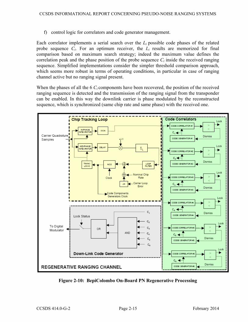
CCSDS INFORMATIONAL REPORT CONCERNING PSEUDO-NOISE RANGING SYSTEMS
CCSDS 414.0-G-2 Page 2-15 February 2014
f) control logic for correlators and code generator management.
Each correlator implements a serial search over the Li possible code phases of the related probe sequence Ci. For an optimum receiver, the Li results are memorized for final comparison based on maximum search strategy; indeed the maximum value defines the correlation peak and the phase position of the probe sequence Ci inside the received ranging sequence. Simplified implementations consider the simpler threshold comparison approach, which seems more robust in terms of operating conditions, in particular in case of ranging channel active but no ranging signal present.
When the phases of all the 6 Ci components have been recovered, the position of the received ranging sequence is detected and the transmission of the ranging signal from the transponder can be enabled. In this way the downlink carrier is phase modulated by the reconstructed sequence, which is synchronized (same chip rate and same phase) with the received one.
Figure 2-10: BepiColombo On-Board PN Regenerative Processing
CCSDS INFORMATIONAL REPORT CONCERNING PSEUDO-NOISE RANGING SYSTEMS
CCSDS 414.0-G-2 Page 2-16 February 2014
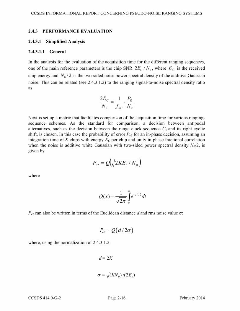
2.4.3 PERFORMANCE EVALUATION
2.4.3.1 Simplified Analysis
2.4.3.1.1 General
In the analysis for the evaluation of the acquisition time for the different ranging sequences, one of the main reference parameters is the chip SNR 0/2 NEC , where CE is the received chip energy and 2/0N is the two-sided noise power spectral density of the additive Gaussian noise. This can be related (see 2.4.3.1.2) to the ranging signal-to-noise spectral density ratio as
00
12NP
fNE R
RC
C ⋅=
Next is set up a metric that facilitates comparison of the acquisition time for various ranging-sequence schemes. As the standard for comparison, a decision between antipodal alternatives, such as the decision between the range clock sequence C1 and its right cyclic shift, is chosen. In this case the probability of error Pe2 for an in-phase decision, assuming an integration time of K chips with energy EC per chip and unity in-phase fractional correlation when the noise is additive white Gaussian with two-sided power spectral density N0/2, is given by
( )02 /2 NKEQP ce =
where
2 / 21( ) 2
t
x
Q x e dtπ
∞−= ∫
Pe2 can also be written in terms of the Euclidean distance d and rms noise value σ:
( )2 / 2eP Q d σ=
where, using the normalization of 2.4.3.1.2.
d = 2K
)2/()( 0 cEKN=σ

CCSDS INFORMATIONAL REPORT CONCERNING PSEUDO-NOISE RANGING SYSTEMS
CCSDS 414.0-G-2 Page 2-17 February 2014
Equivalently, the number Ka of chips needed for a given Pe2 with antipodal sequences having
unity in-phase fractional correlation is ( )[ ] .
2 0
22
1
NEPQK
c
ea
−
=
The number Ka of chips needed for a given Pe2 with antipodal sequences having unity in-phase fractional correlation is very mildly dependent on the value of Pe2 for any specified value of the chip SNR, as demonstrated in reference [2].
Applying the considerations reported in 2.4.3.1.3, it is shown that Pe2 ≈ 5×10⁻⁵ corresponds to a probability of successful acquisition of the ranging sequence of about 0.999 (99.9%) and Ka is about 30000 chips for 0/2 NEC = −33 dB; this is the approximate figure uses in the examples in the following subsections.
For an arbitrary probing sequence, the error probability Pe2 in the decision between the in-phase cyclic shift and one of its out-of-phase cyclic shifts is a function of the in-phase fractional correlation ξ and out-of-phase fractional correlation ψ. The signal-space representation for this situation is shown in figure 2-11. The in-phase cyclic shift and the out-of-phase cyclic shift of the probing sequence correspond to the points C and E, respectively, on the circle of radius Kξ (K being the number of correlated chips).
A
B
D C
d
K( + )/2
E
Kψ
Kξ
Kξξψ
Figure 2-11: Signal-Space Representation for the Decision between the In-Phase Cyclic Shift and One of Its Out-of-Phase Cyclic Shifts of an Arbitrary Probing Sequence of Length K Chips, Having In-Phase Fractional Correlation ξ and Out-of-Phase Fractional Correlation ψ

CCSDS INFORMATIONAL REPORT CONCERNING PSEUDO-NOISE RANGING SYSTEMS
CCSDS 414.0-G-2 Page 2-18 February 2014
Applying simple geometrical considerations to the similar triangles ABC and BCD, the squared Euclidean distance d2 between the signals at points C and E is:
4 222 λξ ⋅⋅⋅= Kd with .2ξψξλ −
=
The parameterλ is the correlation scale factor for the probing sequence. For a decision between antipodal sequences, ψ = −ξ so that λ = 1. For a decision between orthogonal sequences, ψ = 0 so that λ = 1/2.
Using the above expressions and following the approach used above for antipodal signals, it is shown that the number K of chips needed for a given Pe2 and for any specified value of the chip SNR is
( )[ ]
12 2
0
22
1
ξλ ⋅=
−
NEPQK
c
e
This motivates defining the normalized correlation time (τcor) of an arbitrary probing sequence with parameters ξ and ψ as the ratio between K for the arbitrary probing sequence and Ka for antipodal sequence with unity in-phase fractional correlation as
) /(1/ 2 λξτ ⋅== acor KK
Finally assuming an acquisition strategy based on the maximum search and a single correlator for each probing sequence, it is possible to define the normalized acquisition time τacq−Li of the probing sequence Ci as
τacq−Li = Li τcor
where Li is the length of the probing sequence or, equivalently, the number of distinct cyclic shifts of that sequence. To find the normalized total acquisition time τacq-tot, i.e., the normalized time required to acquire the phase of the entire ranging sequence, it can be assumed that all six probing sequences in the ranging-sequence scheme are correlated in parallel during the acquisition process, which requires six correlators. In this case τacq-tot is just the maximum of the normalized acquisition times τacq−Li of the six probing sequences, namely that of C6, so that
τacq-tot = τacq−23
To convert the normalized time values (τcor , τacq−Li , and τacq-tot) to time measured in chips of the probing sequence, it is necessary only to multiply by the number of chips Ka needed to obtain the desired Pe2 at the specified chip SNR for antipodal sequences with unity in-phase fractional correlation.

CCSDS INFORMATIONAL REPORT CONCERNING PSEUDO-NOISE RANGING SYSTEMS
CCSDS 414.0-G-2 Page 2-19 February 2014
Table 2-5 (for v=2 balanced weighted-voting Tausworthe PN ranging-sequence) and table 2-6 (for v=4 balanced weighted-voting Tausworthe PN ranging-sequence) give the normalized correlation time τcor, together with the correlation time in chips (equal to 30000 τcor) required to achieve a pairwise error probability Pe2 = 5×10⁻⁵ at a chip SNR 2EC /N0 of −33 dB.
Table 2-5: v=2 Balanced Weighted-Voting Tausworthe PN Ranging-Sequence
Probing Sequence ξ ψ λ τcor
Correlation Time (Chips)
C1 (range clock)
0.6274 −0.6274 1 2.54 76 200
C2 0.2447 −0.0410 0.5838 28.61 858 300
-C3 0.2481 −0.0247 0.5498 29.55 886 500
-C4 0.2490 −0.0177 0.5355 30.12 903 600
C5 0.2492 −0.0139 0.5279 30.50 915 000
-C6 0.2496 −0.0113 0.5226 30.71 921 300
In-phase fractional correlation ξ, out-of-phase fractional correlation ψ, correlation scale factor λ and normalized correlation time τcor, together with the correlation time in chips required to achieve a pairwise error probability Pe2 = 5×10⁻⁵ at a chip SNR 2EC /N0 of −33.
Table 2-6: v=4 Balanced Weighted-Voting Tausworthe PN Ranging-Sequence
Probing Sequence ξ ψ λ τcor
Correlation Time (Chips)
C1 (range clock)
0.9387 −0.9387 1 1.13 33 900
C2 0.0613 −0.0103 0.5840 455.7 13 671 000
-C3 0.0613 −0.0061 0.5498 484.0 14 520 000
-C4 0.0613 −0.0044 0.5359 496.6 14 898 000
C5 0.0613 −0.0034 0.5277 504.3 15 129 000
-C6 0.0613 −0.0028 0.5228 509.0 15 270 000
In-phase fractional correlation ξ, out-of-phase fractional correlation ψ, correlation scale factor λ and normalized correlation time τcor, together with the correlation time in chips required to achieve a pairwise error probability Pe2 = 5×10⁻⁵ at a chip SNR 2EC /N0 of −33 dB.
Applying the previous equations reveals the total acquisition time in chips to be as in table 2-7. The table indicates also the acquisition time in seconds assuming a chip rate of 2 Mc/s (range clock frequency fRC of 1 MHz and chip duration TC as 0.5 μs)

CCSDS INFORMATIONAL REPORT CONCERNING PSEUDO-NOISE RANGING SYSTEMS
CCSDS 414.0-G-2 Page 2-20 February 2014
Table 2-7: Normalized Acquisition Time (τacq-tot ) and Acquisition Time (Tacq) in Chips and Seconds Assuming fRC=1 MHz and for the Error Probability Pe2 = 5×10⁻⁵ and a Chip Signal-to-Noise Ratio 2EC /N0 of −33 dB
Sequence τacq-tot = τacq−23 =
23 × τcor Tacq (in chips) Tacq (s)
T2B 23 × 30.71 = 706.3
30,000 × 706.3 = 21,189,900
10.59
T4B 23 × 509.0 = 11,707
30,000 × 11,707 = 351,210,000
175.6
It is interesting to observe that for the on-board acquistion time (TACQ_S/C = TACQ Spacecraft) the following general expression applies:
===−
Cacq
c
e
CtotacqaCSACQ FNE
PQF
KT 12
123_
0
22
1
_/_[ ]( ) ττ ··
[ ] [ ]C
corr
C
r
e
FFN
PPQ 12312
0
22
1
=− ( ) ( )
==−
2
0
22
1 1232
NPPQ
r
eτλξ
··
[ ]( )−
=−
2
1232
0
22
1
NPPQ
r
e
ξξ ψ
·
where τcorr , λ and ξ are related to C6 (L6 = 23).
It can be seen that:
– If the acquisition time is given as a function of the Ranging Signal Power over Noise Spectral Density (PR/N0 in dBHz), then the dependence on the chip rate disappears.
– If PR/N0 is reduced by 3 dB (i.e., from 27 to 24 dBHz), the acquisition time increases by a factor of 2, if PR/N0 is increased by 10 dB (i.e., from 27 to 37 dBHz), the acquisition is 10 times smaller. So the values in table 2-7 (evaluated for 27 dBHz) become respectively 5.29 s (for T2B) and 87.8 s (for T4B) for PR/N0 = 30 dBHz. Also the variation of the acqusition time based on the exponential law 10(Pr/No−30)/10 is demonstrated.

CCSDS INFORMATIONAL REPORT CONCERNING PSEUDO-NOISE RANGING SYSTEMS
CCSDS 414.0-G-2 Page 2-21 February 2014
2.4.3.1.2 Normalization and Signal-to-Noise Ratio Definitions
The output of the phase-demodulator for the received ranging-sequence signal can be written as:
)()( tntsPR +
where
CCk kTtTksts ≤<−= )1(for )(
is the binary (±1) ranging-sequence waveform with chip values ks ∈ {+1, –1}, TC is the chip duration, PR is the power in the received ranging waveform, and n(t) is white Gaussian noise with zero mean and autocorrelation function
)(2
)( 0 τδτ NR =
The output at time t = kTC of the matched filter for the rectangular chip waveform is
( 1) ( 1)
1 1( ) ( ) ( )C C
C C
kT kT
R R kk T k TC C
P s t n t dt P s n t dtT T− −
⎡ ⎤+ = +⎣ ⎦∫ ∫
Dividing by RP yields the conveniently normalized matched-filter output
kkk nsr +=
where
( 1)
1 ( )C
C
kT
k k TR C
n n t dtP T −
= ∫
The integral nk is a Gaussian random variable with zero mean.
Since
[ ]∫ ∫∫∫ − −−−=⎥⎦
⎤⎢⎣⎡ C
C
C
C
C
C
C
C
kT
Tk
kT
Tk
kT
Tk
kT
Tkdtdttntndttndttn
)1(
)1( 2121
)1( 22
)1( 11 )()(E)()(E
C
kT
Tk
kT
Tk
kT
TkT
Ndt
Ndtdttt
N C
C
C
C
C
C 2
2 )(
20
)1( 20
)1(
)1( 21210 ==−= ∫∫ ∫ −− −δ
where E[.] denotes the expectation operator, kn is also a zero-mean Gaussian random variable with variance:
CCSDS INFORMATIONAL REPORT CONCERNING PSEUDO-NOISE RANGING SYSTEMS
CCSDS 414.0-G-2 Page 2-22 February 2014
CCRC
CR EN
TPNTN
TP 2221 000
2
==⎟⎟⎠
⎞⎜⎜⎝
⎛
where CRC TPE = is the chip energy. Because 12 ≡ks , it follows that the chip SNR is
chip0 0
2 2SNR R C CP T EN N
= =
Because the range-clock fundamental frequency is
12RC
C
fT
=
the chip SNR can also be written as
RC
R
fNP 1SNR
0chip ⋅=
2.4.3.1.3 Acquisition Probability
The probing sequence Ci will be correctly acquired if and only if its in-phase cyclic shift would win a pairwise contest with each of the Li −1 out-of-phase cyclic shifts of the probing sequence. The probability of error PeLi in acquiring this probing sequence is thus very well approximated as:
PeLi ≈ (Li −1)Pe2
when Pe2 is small. The right side of this equation is always a strict upper bound on PeLi and is also a good approximation of PeLi since the events that the in-phase cyclic shift wins the individual pairwise contests are substantially independent so that:
1 - PeLi = (1 - Pe2) Li −1 ≈ 1 - (Li −1)Pe2
From the above equation it can be seen that the probing sequence C6 has the greatest probability of acquisition error, but its acquisition time is more than 20% longer than that of the other probing sequences. Assuming that all six probing sequences are correlated in parallel and that the correlation time is the one defined by C6, it can be concluded that the probabilities of error in acquiring the other five probing sequences will be much smaller. It follows that correlating all six probing sequences in parallel over the required correlation time for probing sequence C6, makes it possible to neglect the probability of erroneous acquisition of the other five probing sequences and conclude that
PACQ ≈ 1 - Pe23 ≈ 0.999

CCSDS INFORMATIONAL REPORT CONCERNING PSEUDO-NOISE RANGING SYSTEMS
CCSDS 414.0-G-2 Page 2-23 February 2014
which is the target probability of successful acquisition. This results in Pe23 ≈ 1.1×10⁻³. Since the integraton time for C6 is also used for the other sequences, PeLi will decrease progressively from C5 to C1.
2.4.3.2 Accurate Analysis
A more accurate analysis for the on-board acquisition performances is based on the same approach applied in 2.6.3.2 for the ground station case.
( )∫∞
∞−
−
⎥⎦⎤
⎢⎣⎡ −−⋅⎥⎦
⎤⎢⎣⎡ −= dyyyerfcCP
iL
i
21
exp1)(211)( γ
π
where P(Ci) is the probability of correct decision on each code Ci and
( ) )( 6
1∏=
≅i
iACQ CPCP
)(1)( xerfxerfc −=
dtexerfx
t∫ −=0
22)(π
However, for the on-board mixed serial/parallel architecture, since each probing sequence Ci is acquired using a serial algorithm, the noise component for the Li different correlations can be assumed statistically independent4. Therefore, in this case
CORTN2
02 =ησ
and
CORRii
c
CORcii TNP
LTT
NE
L 0
210
0
210
⎟⎟⎠
⎞⎜⎜⎝
⎛ −=⎟⎟
⎠
⎞⎜⎜⎝
⎛ −=
∗∗∗∗ ρρρργ
where ρ*ik are the normalized correlation coefficients defined in 2.6.3.2.
For the on-board receiver, it can be observed that the correlation time for code Ci is TCOR,i = TACQ/Li, since Li phases are serially processed in the time interval TACQ. As an example, the correlation time applied for code C2 is 23/7 of the correlation time of the code C6 and as a consequence P(C2) >> P(C6). So one can conclude that for the on-board acquisition scheme PACQ ≈ P(C6), and TACQ = 23×TCOR6. The required correlation time TCOR6 for a probability of
4 This is the reason why the simplified analysis and the accurate analysis provide similar results for on-board applications when the serial algorithm is applied for each probing sequence Ci.

CCSDS INFORMATIONAL REPORT CONCERNING PSEUDO-NOISE RANGING SYSTEMS
CCSDS 414.0-G-2 Page 2-24 February 2014
successful acquisition PACQ equal to 99.9 % is obtained by inverting the second equation in this subsection but practically the same results are obtained by inverting the first one with i = 6 (the relative error is lower than 0.3% for this PACQ value).
2.4.3.3 Simplified versus Accurate Analysis
The theoretical acquisition time values specified in the Blue Book have been derived using the expressions and procedure reported in 2.4.3.2.
However, following the simplified approach of 2.4.3.1 and observing that
– the values of table 2-7 are related to 2Ec/N0=−33 dB or PR/N0=27 dBHz, and
– the acquisition time at 30 dBHz is one half of the acquisition time at 27 dBHz,
one finds 87.8 s for T4B and 5.3 s for T2B. This corresponds to an error of about 2% when compared with the accurate analysis results. It must be underlined that the simplified analysis is correct from a theoretical point of view,5 but because of some approximations in the calculations there is such small discrepancy in the final result. However, it is very useful since it allows finding a final closed expression for the acquisition time showing the impacts due to the SNR and the code coefficients ξ and ψ.
2.4.4 ON-BOARD H/W IMPLEMENTATIONS AND LIMITATIONS
The theoretical evaluations reported in 2.4.2 and 2.4.3 are based on a set of assumptions reported in 2.4.1, in particular:
– No quantization effects at the matched filter output.
– Code detection implemented using the maximum search algorithm.
In order to limit the DSP complexity the number of bits for signal representation at the matched filter output must be properly limited. The hard quantization (1 bit only) clearly minimizes the gate number but introduces additional losses in the acquisition performances. The 3-bit quantization represents a good compromise in terms of performances versus complexity.
The algorithm based on the maximum search represents the optimum approach (in terms of acquisition performances) for PN signal acquisition. However, this algorithm shows a limitation: also in absence of a useful input signal (i.e., with noise only) it will find a maximum.
It is true that code acquisition is executed after the CTL has declared the lock condition, but a false CTL lock could generate a false PN acquisition. To minimize this false probability one of the following approaches can be applied (for each of the Ci sequences):
5 This is not true for the station acquisition performances when implementing full parallel receiver.

CCSDS INFORMATIONAL REPORT CONCERNING PSEUDO-NOISE RANGING SYSTEMS
CCSDS 414.0-G-2 Page 2-25 February 2014
a) Approach Based on Confirmation of the Acquisition
Different solutions can be proposed, for instance:
– to confirm the PN code acquisition comparing the selected maximum value with a predefined threshold (including S+N normalization using a dedicated ranging AGC);
– to confirm the PN code acquisition checking the difference (in amplitude) between the selected maximum value and the other Li −1 values: acquisition confirmed if the difference is bigger than a predefined threshold;
– entering the tracking mode and continuously checking if the acquired code phase corresponds to the maximum for each Ci codes; PN acquisition could be declared achieved after some confirmations, for instance n success over k trials.
b) Approach Based on Proper Link Procedure
– to apply the ranging modulation on the uplink signal before enabling the on-board ranging channel: in this way the ranging processor never processes the noise alone.
For the first approach the acquisition process is (in practice) terminated when confirmation has been achieved; only at this point the turnaround function can be enabled with the application of the regenerated PN ranging signal at the downlink modulator.
An additional approach could be to replace the maximum search algorithm with the fixed threshold comparison. Of course, to optimize the performances versus different input signal power levels, S+N normalization using a dedicated ranging AGC is required. However, in the usual case where the in-phase cyclic shift is orthogonal (or nearly so as in figure 2-12) to the out-of-phase cyclic shift, the squared length of the line segment CB is twice (or nearly so) the squared length of the line segment CD. This means that one pays approximately 3 dB penalty in the required SNR to achieve a specified performance when one uses the best fixed-threshold decision rule instead of the optimum decision rule (i.e., maximum search). Only for antipodal signals (i.e., the clock component) there is no loss when using the best fixed-threshold decision rule.

CCSDS INFORMATIONAL REPORT CONCERNING PSEUDO-NOISE RANGING SYSTEMS
CCSDS 414.0-G-2 Page 2-26 February 2014
A
B
D C
d
K
Kξ
KξK( + )/2
E
Decision boundaryfor fixed threshold
Boundary foroptimum decision
received segment
ψ
ψ
ξ
Optimum Decision Boundary = Maximum Search
Figure 2-12: Space Representation for the Probe Sequence Ci and Decision Boundaries
In case of fixed threshold comparison, the threshold shall be defined considering the correct acquisition but also the false acquisition (for out-of phase correlation) probability.
The comparison between the maximum search and the Threshold Comparison acquisition procedures is shown in table 2-8 in terms of a loss in dB for the same acquisition probability (PACQ =PACQ_equiv= 99.9%). The loss for the three cases of threshold comparison is defined as the required additional dB with respect to a PR/N0 = 27 dBHz in order to have the maximum acquisition time obtained by Threshold Comparison equal to the acquisition time obtained by the maximum search (see reference [13]).
CCSDS INFORMATIONAL REPORT CONCERNING PSEUDO-NOISE RANGING SYSTEMS
CCSDS 414.0-G-2 Page 2-27 February 2014
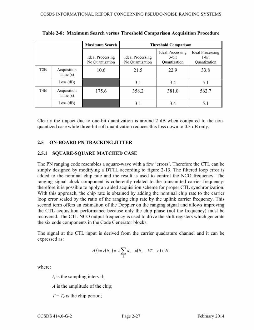
Table 2-8: Maximum Search versus Threshold Comparison Acquisition Procedure
Maximum Search Threshold Comparison
Ideal Processing No Quantization
Ideal Processing No Quantization
Ideal Processing 3-bit
Quantization
Ideal Processing 1-bit
Quantization
T2B Acquisition Time (s)
10.6 21.5 22.9 33.8
Loss (dB) 3.1 3.4 5.1 T4B Acquisition
Time (s) 175.6 358.2 381.0 562.7
Loss (dB) 3.1 3.4 5.1
Clearly the impact due to one-bit quantization is around 2 dB when compared to the non- quantized case while three-bit soft quantization reduces this loss down to 0.3 dB only.
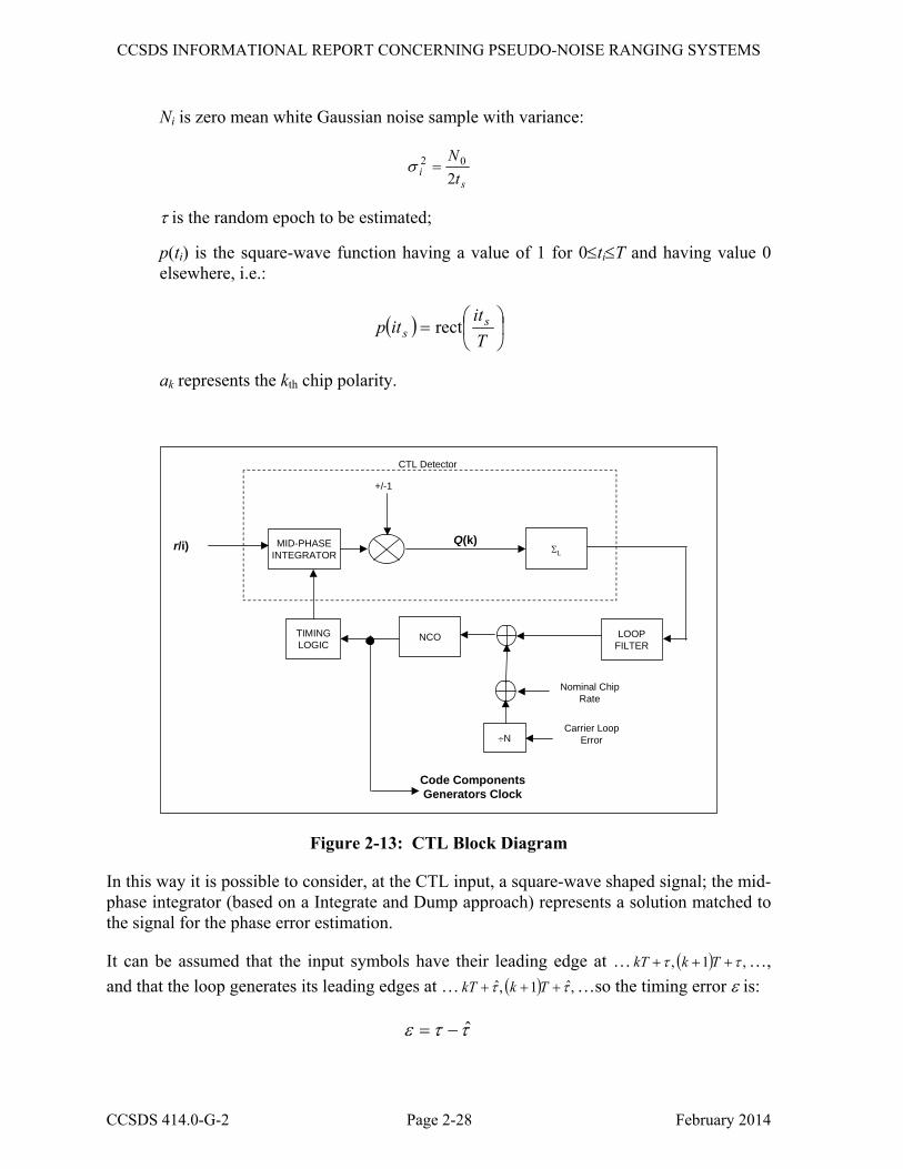
2.5 ON-BOARD PN TRACKING JITTER
2.5.1 SQUARE-SQUARE MATCHED CASE
The PN ranging code resembles a square-wave with a few ‘errors’. Therefore the CTL can be simply designed by modifying a DTTL according to figure 2-13. The filtered loop error is added to the nominal chip rate and the result is used to control the NCO frequency. The ranging signal clock component is coherently related to the transmitted carrier frequency; therefore it is possible to apply an aided acquisition scheme for proper CTL synchronization. With this approach, the chip rate is obtained by adding the nominal chip rate to the carrier loop error scaled by the ratio of the ranging chip rate by the uplink carrier frequency. This second term offers an estimation of the Doppler on the ranging signal and allows improving the CTL acquisition performance because only the chip phase (not the frequency) must be recovered. The CTL NCO output frequency is used to drive the shift registers which generate the six code components in the Code Generator blocks.
The signal at the CTL input is derived from the carrier quadrature channel and it can be expressed as:
( ) ( ) ( ) ik
sks NkTitpaAitrir +−−⋅== ∑ τ
where:
ts is the sampling interval;
A is the amplitude of the chip;
T = Tc is the chip period;
CCSDS INFORMATIONAL REPORT CONCERNING PSEUDO-NOISE RANGING SYSTEMS
CCSDS 414.0-G-2 Page 2-28 February 2014
Ni is zero mean white Gaussian noise sample with variance:
si t
N2
02 =σ
τ is the random epoch to be estimated;
p(ti) is the square-wave function having a value of 1 for 0≤ti≤T and having value 0 elsewhere, i.e.:
( ) ⎟⎠
⎞⎜⎝
⎛=
Tit
itp ss rect
ak represents the kth chip polarity.
MID-PHASEINTEGRATOR
NCOTIMINGLOGIC
r/i)
LOOPFILTER
ΣL
÷NCarrier Loop
Error
Nominal ChipRate
Code ComponentsGenerators Clock
+/-1
CTL Detector
Q(k)
Figure 2-13: CTL Block Diagram
In this way it is possible to consider, at the CTL input, a square-wave shaped signal; the mid-phase integrator (based on a Integrate and Dump approach) represents a solution matched to the signal for the phase error estimation.
It can be assumed that the input symbols have their leading edge at … ( ) ,1 , ττ +++ TkkT …, and that the loop generates its leading edges at … ( ) ,ˆ1 ,ˆ ττ +++ TkkT …so the timing error ε is:
ττε ˆ−=

CCSDS INFORMATIONAL REPORT CONCERNING PSEUDO-NOISE RANGING SYSTEMS
CCSDS 414.0-G-2 Page 2-29 February 2014
Now the tracking performance of the CTL in terms of timing jitter, namely .2εσ , can be
determined.
Using linear theory, 2εσ can be derived once the following two quantities are determined:
a) the loop S-curve;
b) the two-sided spectral density of the equivalent additive noise.
The S-curve is defined as the mean value of the error control signal conditioned on the timing error. Mathematically:
( ) ( )εε kQELS ⋅=
where E( • ) denotes the statistical expectation, Qk = Q(k) is the quadrature channel output (see figure 2-13) and L represents the accumulation length of the integrate-&-dump following the quadrature branch of the CTL. The mid-phase integrator output is given by (see figure 2-14):
( ) ( )[ ]{ }∑∑∈∈
+−−⋅==kk Ci
iskCi
k NkTitpaAirQ τ
where:
⎭⎬⎫
⎩⎨⎧
+⎟⎠⎞
⎜⎝⎛ +<≤+⎟
⎠⎞
⎜⎝⎛ −= ττ ˆ
21ˆ
21: TkitTkiC sk
The mid-phase integrator output is multiplied by ±1 in order to provide the right correction to the loop. In a certain way the multiplication by ±1 replaces the transition detector considering that the PN sequence resembles a square-wave. The mean value of the mid-phase integrator output after multiplication by +1/−1 is easily found:
( ) 2 ⎟⎟⎠
⎞⎜⎜⎝
⎛⋅=
sk t
AQE ε
( ) ⎟⎟⎠
⎞⎜⎜⎝
⎛=
stALS εε 2
The obtained relationship for the S-curve is meaningful when the loop is tracking. Besides, because of the nature of the accumulation, ε is always quantized to an integer multiple of the sampling period ts; however, the presence of noise makes the quantization effect negligible, if the number of samples per chip is high enough. The slope of the S-curve at the origin represents the loop detector gain Kε:

CCSDS INFORMATIONAL REPORT CONCERNING PSEUDO-NOISE RANGING SYSTEMS
CCSDS 414.0-G-2 Page 2-30 February 2014
( )stALSK 2
0=
∂∂
==ε
ε εε
To evaluate the loop equivalent additive noise, it is assumed the CTL is tracking (ε→0). Under this assumption the variance at the phase detector output is:
( )2
002
22Var
ssskN
tTN
LtT
tN
LQL ⋅=⎟⎟⎠
⎞⎜⎜⎝
⎛=⋅=σ
The loop timing jitter 2εσ can be estimated using a linearized model of the CTL. With this
approach, the loop error η at the phase detector output can be written as:
NK +⋅= εη ε
being N the additive Gaussian noise. The above relationship leads to the equivalent linearized loop reported in figure 2-15.
Time
Ampl
itude
τ+⎟⎠⎞
⎜⎝⎛ − Tk
21
τ+⎟⎠⎞
⎜⎝⎛ + Tk
21
ts
τ̂21
+⎟⎠⎞
⎜⎝⎛ − Tk
τ̂21
+⎟⎠⎞
⎜⎝⎛ + Tk
Mid-Phase Integration Windowε
ε
Figure 2-14: Mid-Phase Integration
CCSDS INFORMATIONAL REPORT CONCERNING PSEUDO-NOISE RANGING SYSTEMS
CCSDS 414.0-G-2 Page 2-31 February 2014
NCO
+
+
+
-
N/Kε
Kετ
τ̂
ε
Loop Filter
η
Figure 2-15: Linearized Loop Model (Synchronization Error Expressed As Timing Error)
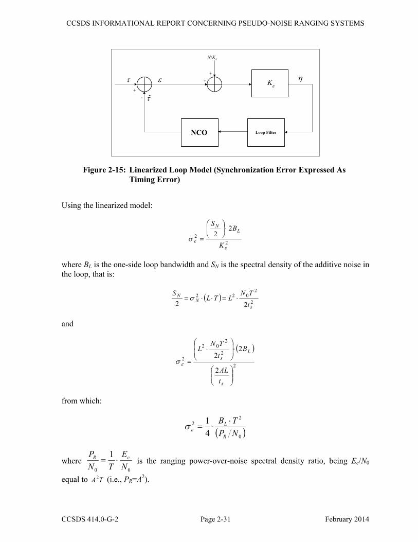
Using the linearized model:
22
22
εεσ K
BS
LN ⋅⎟⎠
⎞⎜⎝
⎛
=
where BL is the one-side loop bandwidth and SN is the spectral density of the additive noise in the loop, that is:
( )2
2022
22 sN
N
tTN
LTLS
⋅=⋅⋅= σ
and
( )
2
2
202
2
2
22
⎟⎟⎠
⎞⎜⎜⎝
⎛
⋅⎟⎟⎠
⎞⎜⎜⎝
⎛⋅
=
s
Ls
tAL
BtTN
L
εσ
from which:
( )0
22
41
NPTB
R
L ⋅⋅=εσ
where 00
1NE
TNP cR ⋅= is the ranging power-over-noise spectral density ratio, being Ec/N0
equal to TA2 (i.e., PR=A2).

CCSDS INFORMATIONAL REPORT CONCERNING PSEUDO-NOISE RANGING SYSTEMS
CCSDS 414.0-G-2 Page 2-32 February 2014
In the above calculation it has been assumed all the power of the ranging signal as useful power for the CTL, but in reality, because of the CTL filtering action, only the clock component is used for the tracking of the chip rate. So, replacing the ranging power PR with the power associated to the clock component PRC and considering that the frequency of the ranging clock component fRC is half of the chip rate value (FC = 1/Tc=2fRC):
RC
oL
RC PNB
f⋅=
41
εσ [s]
Finally, the one-way ranging jitter can be written as:
( )0___ 82 NP
Bfcc
RC
L
RCsqsqCTLRange ⋅== εσσ [m]
being c the speed of the light.
2.5.2 SINE-SQUARE MISMATCHED CASE
It must be underlined that the above analysis is based on a square-wave shaped signal and a matched receiver; in most of the cases the channel (in particular the transmit and the receive analogue front-ends) implements a filtering action removing the higher code (and ranging clock) components. For instance, assuming a chip rate of 3 Mc/s and a receiver with approximately an IF bandwidth of 6 MHz, all the clock spectral components of order higher than 1 are strongly affected by filtering action. As worst case one can consider that, because of this filtering, the ranging sequence appears as sine-wave shaped at the CTL input. In this case, assuming just the fundamental clock component, one has to consider additional power loss and SNR reduction at demodulator input (resulting from the RF front-end). For instance, one has to remember that 81% of the overall power of square-wave signal is related to the fundamental or first component.
However, in the following an ideal sine-wave shaped ranging signal (neglecting the losses due to channel filtering) is considered, and focus is on the CTL performances.
In this case the expression for the S curve above provided (see 2.5.1) is not valid anymore. To evaluate it, as in figure 2-14, two consecutive chips of different polarity sine-waved shaped with amplitude A2 are considered: this corresponds to a sinusoidal signal clock of power A2. Again a synchronization error is assumed (in the square-shaped Mid-phase integration) equal to ε:
s
sKN
K tA
TtnA επ 222cos2
)2/(
≈⎟⎠⎞
⎜⎝⎛ ⋅∑
+
where ε=Kts and T=Nts. The above approximation is valid in tracking in case of small errors ε. Therefore:

CCSDS INFORMATIONAL REPORT CONCERNING PSEUDO-NOISE RANGING SYSTEMS
CCSDS 414.0-G-2 Page 2-33 February 2014
( ) 22 ⎟⎟⎠
⎞⎜⎜⎝
⎛⋅=
sk t
AQE ε
( ) ⎟⎟⎠
⎞⎜⎜⎝
⎛=
stALS εε 22
( )stALSK 22
0
=∂
∂=
=εε ε
ε
Considering that for the noise terms the same equations of the square-matched case and applying the same considerations for the ranging clock power and the ranging clock frequency:
RC
oL
RC PNB
f⋅=
41
21
εσ (s)
Finally, the one-way ranging jitter can be written as:
( )0sin___ 82
12 NP
Bfcc
RC
L
RCsqCTLRange ⋅== εσσ [m]
2.5.3 COMPARISON OF SINE AND SQUARE SHAPING PERFORMANCE
As described and derived in 2.5.1 the performances of the CTL expressed in terms of time tracking jitter ( )sqsq __εσ are:
RC
oL
RCsqsq P
NBf
⋅=4
1__εσ [s]
where:
– fRC is the frequency of the ranging clock (half of the chip rate value), (Hz);
– PRC is the power of the ranging clock component (square-wave in this case) at CTL input (W);
– N0 is the one-sided noise power spectral density (W/Hz) at CTL input;
– BL is the one-sided loop noise bandwidth of the CTL (Hz).
This expression is related to the square-wave signal and matched receiver (square-shaped integrated and dump filtering for the Mid-phase integrator) under the following conditions:
– ideal CTL;

CCSDS INFORMATIONAL REPORT CONCERNING PSEUDO-NOISE RANGING SYSTEMS
CCSDS 414.0-G-2 Page 2-34 February 2014
– no impacts due to time quantization (number of samples per chip);
– soft quantization of the chip detection filter (matched filter);
– no interference contribution due to telecommand.
For the one-way ranging rms error:
( )0___ 8 NP
Bfc
RC
L
RCsqsqCTLRange ⋅=σ [m]
where c is the speed of the light (m/s).
In case of sine-wave shaped ranging sequence (see 2.5.2) and assuming the same ideal conditions above mentioned, the CTL performances (still implemented using a square-wave shaped Mid-Phase integrator) become:
RC
oL
RCsqe P
NBf
⋅=4
12
1_sin_εσ [s]
( )0_sin__ 82
1NP
Bfc
RC
L
RCsqeCTLRange ⋅=σ [m]
where PRC is the power of the sinusoidal clock component at CTL input.
Therefore the following relation exists:
2 __
_sin_sqsq
sqeε
ε
σσ =
The sine-square expression are applicable in case of sine-wave shaped signal in transmission, but can be applied also (as limit condition) for the situation when the square-wave shaped transmitted signal is strongly filtered in the receiver side before the CTL. In the latter case, the expression takes into account only the performances of the CTL and neglects any contribution (in terms of degradation) due to the channel filtering. Indeed in the above expressions PRC/N0 represents the power of the ranging clock (assumed sinusoidal as limit case) over noise spectral density at the CTL input.
As derived in 2.7.2.3, the one-way ranging rms error for the case of sinewave shaping with matched receiver is:
( )0_sin__ 4
1NP
Bfc
RC
L
RCsneeCTLRange ⋅=
πσ [m]
In the same conditions indicated in the Blue Book, the following is obtained:

CCSDS INFORMATIONAL REPORT CONCERNING PSEUDO-NOISE RANGING SYSTEMS
CCSDS 414.0-G-2 Page 2-35 February 2014
– BL=1 Hz;
– chip rate Fc = 2.068 Mchip/s (fRC= Fc/2);
– PR/N0 =30 dBHz:
a) T4B: ( ) 45.2920 11000 ≈−= ξLOGNPNP RRC dBHz;
b) T2B: ( ) 95.2520 11000 ≈−= ξLOGNPNP RRC dBHz.
And finally:
Table 2-9: Station Ranging Jitter Performances
Sequence sine_sine__ CTLRangeσ sqCTLRange _sine__σ sqsqCTLRange ___σ
T4B 0.78 m 0.87 m 1.22 m
T2B 1.17 m 1.29 m 1.82 m
As above underlined, the expressions for the on-board tracking jitter are relevant to a theoretical CTL behavior; for this reason the Blue Book specifies in addition a value of 2 dB for the implementation losses. These losses take into account the contributions due to signal quantization and non-perfect carrier tracking and signal demodulation.
Concerning the signal quantization effects: the signal amplitude quantization (in terms of number of bit), the time sampling (i.e., finite number of samples per chip) and the chip asymmetry.
The effects due to amplitude quantization and the chip asymmetry can be considered in general negligible. Different is the situation for the time sampling. Taking into account that the sampling frequency is equal to FS, this contribution ( Qεσ ) can be estimated as:
SQ F
1121
=εσ (s)
For instance, at FS = 20 MHz there is an rms error of 14 ns (2.1 m one-way), bigger than the theoretical values related to the thermal noise at PR/N0=30 dBHz and for BL=1 Hz. Concerning the time sampling contribution:
– it is constant and independent from the signal to noise ratio’
– at low loop SNR, it is masked by the jitter due to the thermal noise;
– as the thermal jitter, it can be reduced with average processing at ground station.

CCSDS INFORMATIONAL REPORT CONCERNING PSEUDO-NOISE RANGING SYSTEMS
CCSDS 414.0-G-2 Page 2-36 February 2014
Finally the Blue Book (reference [1]) specifies as reference point for the on-board ranging jitter the theoretical performances for a CTL loop bandwidth BL of 1Hz. In case of wider on-board loop bandwidth6 implementation, the theoretical jitter values can be recalculated using the following expression:
LHzB BL 1σσ =
The implementation loss smaller than 2 dB shall be referred to these new theoretical jitter values.
2.6 STATION ACQUISITION
2.6.1 INTRODUCTION
The theoretical on-board acquisition time and the analysis reported in this subsection are based on an ideal linear channel and a station processing implementing:
a) full parallel approach based on 76 parallel correlators;
b) maximum search algorithm;
NOTE – It is shown (see on-board analysis in 2.4.4) that the maximum search corresponds to the optimum receiver solution.
c) perfect carrier demodulation (the carrier tracking loop jitter degradation is not considered);
d) perfect chip tracking (the CTL jitter degradation is not considered);
e) no impacts due to amplitude quantization of the signal at the output of the chip detection filter (matched filter);
f) no impacts due to time quantization (number of samples per chip).
In addition the degradation due to downlink telemetry interference (although negligible) is not considered in this analysis, it is reported in 2.8.
2.6.2 STATION DSP ARCHITECTURE FOR PN RANGING PROCESSING
The Station PN ranging operations are accomplished in two stages: first the received ranging clock component is acquired and once this has taken place, the ranging code position is searched, acquired, and tracked.7
6 The specification for the on-board CTL loop bandwidth is mission dependent. 7 For the end-to-end delay measurement with the comparison between the transmitted (uplink) and received (downlink) code epoch.
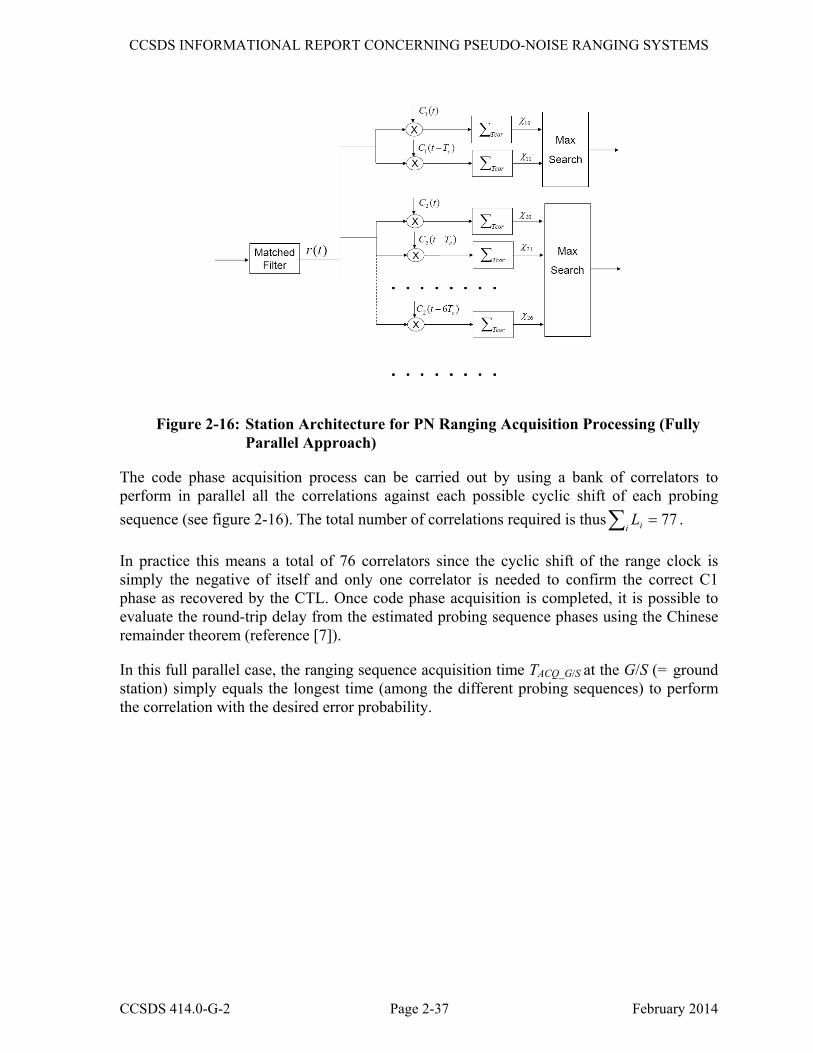
CCSDS INFORMATIONAL REPORT CONCERNING PSEUDO-NOISE RANGING SYSTEMS
CCSDS 414.0-G-2 Page 2-37 February 2014
Figure 2-16: Station Architecture for PN Ranging Acquisition Processing (Fully
Parallel Approach)
The code phase acquisition process can be carried out by using a bank of correlators to perform in parallel all the correlations against each possible cyclic shift of each probing sequence (see figure 2-16). The total number of correlations required is thus 77=∑i iL .
In practice this means a total of 76 correlators since the cyclic shift of the range clock is simply the negative of itself and only one correlator is needed to confirm the correct C1 phase as recovered by the CTL. Once code phase acquisition is completed, it is possible to evaluate the round-trip delay from the estimated probing sequence phases using the Chinese remainder theorem (reference [7]).
In this full parallel case, the ranging sequence acquisition time TACQ_G/S at the G/S (= ground station) simply equals the longest time (among the different probing sequences) to perform the correlation with the desired error probability.

CCSDS INFORMATIONAL REPORT CONCERNING PSEUDO-NOISE RANGING SYSTEMS
CCSDS 414.0-G-2 Page 2-38 February 2014
2.6.3 PERFORMANCE EVALUATION
2.6.3.1 Simplified Analysis
Making reference to the full parallel approach described in 2.6.2 and applying the results of the simplified analysis for the evaluation of the on-board acquisition performances of 2.4.3.1, the following can be written (see references [2] and [5]):
[ ]
⎪⎪⎭
⎪⎪⎬
⎫
⎪⎪⎩
⎪⎪⎨
⎧
⎟⎠⎞
⎜⎝⎛ −⋅
×⋅
−
2
1
20
22
1
/_ii
ir
eiSGACQ ψξ
ξNP
)(PQMAX=T
This closed form expression represents only an approximation for the station acqusition time8. In particular, for the derivation of this expression, the noise terms at the correlator output are assumed statistically independent (among the different correlators of the full parallel scheme). This is not true.
The above equation indicates that TACQ_G/S is shorter than TACQ_S/C by a factor L6 for the same PR/N0.
Assuming the correlator outputs as statistically independent for this parallel acquisition strategy, the probability of successful acquisition can be approximated by PACQ ≈1-22·Pe2.
2.6.3.2 Accurate Analysis
As indicated in 2.6.2, the acquisition process consists in finding the correct phase of the probing sequences Ci by correlating the received signal r(t) (combination of PN ranging signal S(t) plus noise n(t)) against a local model of each probing sequence Ci and all of its cyclic shifts. The correlation χik for time TCOR against the k-th shift of code Ci can be described as:
∫∫∫ +=−⋅+−⋅=−⋅CORCORCOR T
ikikci
T
ci
T
ciik dtkTtCtndtkTtCtSdtkTtCtr=000
)()()()()()( ηρχ
The shift by k chips (k = 0, 1, 2,…, Li −1) that gives the greatest correlation value χik is selected as the one which is in-phase with the received sequence. While ηik is merely the noise contribution at the correlator output, the component ρik represent the correlation value of the received PN sequence S(t) with a unit amplitude and shifted version of Ci after the correlation time TCOR. Assuming a ranging signal power PR = Ec/Tc, the coefficients ρik can be calculated as 8 The analysis behind this expression provides good performances estimation for the on-board mixed parallel/serial approach.
CCSDS INFORMATIONAL REPORT CONCERNING PSEUDO-NOISE RANGING SYSTEMS
CCSDS 414.0-G-2 Page 2-39 February 2014
r
CORikccci
T
c
cik T
TTEdtkTtCtsTE COR
⋅⋅=−⋅⋅= ∫ *
0
)()( ρρ
where:
– )()( tsTEtS
c
c ⋅= and CCk kTtTksts ≤<−= )1(for )( are the binary (±1) ranging-
sequence waveform with chip values ks ∈ {+1, –1};
– TC is the chip duration;
– Tr = LTc is one sequence length;
– ρ*ik are the normalized correlation coefficients (i.e., unit amplitude and correlation
time equal to one sequence length Tr = LTc).
As indicated in table 2-10, the normalized correlation coefficients are related to the in-phase (ξ) and out-of-phase (ψ ) fractional correlation coefficient as defined in 2.4.3
Table 2-10: Normalized Correlation Coefficients (Unit amplitude and Correlation Time Equal to One Sequence Length Tr)
ρ*10=Lξ1 ρ*
11=Lψ1 ρ*20=Lξ2
ρ*2k=Lψ2
(k =1..6) ρ*30=Lξ3
ρ*3k=Lψ3
( k=1..10) T2B 633306 − 633306 247020 − 41404 250404 − 24900 T4B 947566 − 947566 61904 − 10368 61904 − 6160
ρ*40=Lξ4
ρ*4k=Lψ4
k = 1..14 ρ*50=Lξ5
ρ*5k Lψ5
(k =1..18) ρ*6=Lξ6
ρ*6k =Lψ6
(k = 1..22) T2B 251332 − 17852 251604 − 14056 251940 − 11388 T4B 61904 − 4400 61904 − 3456 61904 − 2800
For code C1, assuming that k = 0 is the true phase, the probability of correct decision is simply9:
⎟⎟⎠
⎞⎜⎜⎝
⎛⋅⋅−=>+=>=
COR
cc
r
COR
TNTE
TTerfcPPCP
0
*101010101 2
11)0()0()( ρηρχ
being η10 Gaussian with zero mean and variance 2
0 CORTN 10.
9 Noting that C1 is antipodal and that both k = 0 and k = 1 are equally probable. 10 The erfc(x) function is defined in 2.4.3.2.

CCSDS INFORMATIONAL REPORT CONCERNING PSEUDO-NOISE RANGING SYSTEMS
CCSDS 414.0-G-2 Page 2-40 February 2014
For i >2 (i.e., for C2, ... C6), the random variables ηik are still Gaussian with zero mean and
variance 2
0 CORTN , but they are no longer independent since Cik(t) = Ci(t−kTc) is not
orthogonal to Cih(t) for k ≠ h11. However, it is possible to write )()()( ' tbtCtC ikik += , with
∑−
=
⋅+±
=1
0)(
11)(
iL
jij
i
i tCLL
tb
so that )(' tCik are now orthogonal. Therefore it is possible to write
ikik
T
ikik dttCtr=COR
ηρχ +=⋅∫0
)()(
[ ] ηηη +=⋅+⋅=+⋅ ∫∫∫ '
00
'
0
' )()()()()( ik
TT
ik
T
ikik
CORCORCOR
dttbtndtCtndttbCtn=
being 'ikη independent Gaussian random variables with variance:
CORi
TL
N⋅⎥
⎦
⎤⎢⎣
⎡+=
112
02'η
σ
The probability of correct decision (for the probe sequence Ci) is then given by:12
{ } { }{ }'
1'1
'010
'11
'11
'000110
,,max(
),,max()/,,max()(
−
−−−
>+−=
++>+=>=
i
iii
Lii
LiLiiiiLiii
P
PCPCP
ηηηρρ
ηρηρηρχχχ
…
……
where ρi2 = ρi3 =… = ρiLi −1 are used.
Noting that the cumulative probability distribution is13
{ }( ) ( ) ( ) ( )1
'1
'2
'1
'1
'1
'2211,...,max
−
−−⎥⎥⎦
⎤
⎢⎢⎣
⎡−=≤≤≤=≤
i
ii
L
LLxerfcxPxPxPxP
ησ
ηηηηη …
and that the probability density function of x = ρi0 − ρi1 + η'0 is
11 In addition for the parallel processor of figure 2-16 the same (correlated) input noise sample are processed by the different Li correlators for the maximum search. 12 Assuming that k = 0 , k = 1... k=Li −1 are equally probable. In the following to simplify the expressions the double index (i, k) is removed so that ηk=ηik. 13 The statistical independence of the η'k noise components is exploited.

CCSDS INFORMATIONAL REPORT CONCERNING PSEUDO-NOISE RANGING SYSTEMS
CCSDS 414.0-G-2 Page 2-41 February 2014
( ) ( )[ ]⎥⎥⎦
⎤
⎢⎢⎣
⎡ −−−= 2
210
2'' 2
exp2
1
ηησ
ρρπσ
iixxP
it is possible to write the probability of correct decision on the code phase of sequence Ci as the integral over all possible values of x; i.e.:
( )[ ]∫∞
∞−
−
⎥⎥⎦
⎤
⎢⎢⎣
⎡ −−−⋅
⎥⎥⎦
⎤
⎢⎢⎣
⎡−= dxxxerfcCP ii
L
i
i
2
210
2
1
''' 2exp
21
2211)(
ηηησ
ρρπσσ
with ρi0, ρi1 and σ'η functions of TCOR as given above.
Defining ( )'2/η
σxy = , ( ) 2210 '2
ησρργ ii −= one finds:
( )∫∞
∞−
−
⎥⎦⎤
⎢⎣⎡ −−⋅⎥⎦
⎤⎢⎣⎡ −= dyyyerfcCP
iL
i
21
exp1)(211)( γ
π
where
CORRNG
i
iii
c
CORc
i
iii TN
PL
LLT
TNE
LL
L 0
210
0
210
11 +⎟⎟⎠
⎞⎜⎜⎝
⎛ −=
+⎟⎟⎠
⎞⎜⎜⎝
⎛ −=
∗∗∗∗ ρρρργ
Finally the acquisition process of the full PN ranging sequence is completed successfully when all of the local generated probing sequences Ci are in-phase with the received ranging sequence or14
( ) )( 6
1∏=
≅i
iACQ CPCP .
For the ground station parallel receiver all the correlations are evaluated for the same amount of time and the acquisition time TACQ is equal to TCOR in the above equations. The required correlation time TCOR for a probability of successful acquisition PACQ equal to 99.9 % is obtained by inverting the equation above.
2.6.3.3 Comparison of Approximate and Accurate Analysis
The theoretical acquisition time values specified in the Blue Book (reference [1]) have been derived using the accurate expressions and procedure reported in 2.6.3.2.
However, following the simplified approach and observing that:
14 The decisions on the phases of the probing sequences are correlated, but this correlation can be practically neglected.

CCSDS INFORMATIONAL REPORT CONCERNING PSEUDO-NOISE RANGING SYSTEMS
CCSDS 414.0-G-2 Page 2-42 February 2014
– the values are related to 2Ec/N0= −33 dB or PR/N0= 27 dBHz;
– the acquisition time at 30 dBHz is one half of the acquisition time at 27 dBHz;
– the normalized correlation time is longer (maximum) for the C6 probe sequence, so it defines the overall acquisition time;
– for the fully parallel approach the acquisition time is 1/23 the acquisition time for the on-board case;
one finds 3.87 s for T4B and 0.23 s for T2B at PR/N0 of 30 dBHz. This corresponds to an error of about 10% when compared with the accurate analysis results. As above underlined, the simplified analysis is not correct from a theoretical point of view, since it considers that the noise terms at the correlator output are statistically independent (among the different correlators of the full parallel scheme). However, it is very useful since it allows finding a final closed expression for the acquisition time showing the impacts due to the SNR and the code coefficients ξ and ψ.
In practice, the acquisition performance at the station is affected by the on-board non-linearity (reference [8]) which causes a degradation in the correlation coefficients (ξi, ψi) of the sequence resulting in an increase in the acquisition time. This effect can be equivalently attributed to a decrease of PR/N0: simulations show that non-linear system yields an additional loss of about 0.7 dB with very small differences among the various codes. In principle the same applies for the uplink, but as the transmit channel at the station is much more linear, the increase in acquisition time is negligible in this case.
Table 2-11 below shows the comparison between the values computed using the exact formula and the approximation at the reference point of 30 dBHz for the case of 76 correlators.
Table 2-11: Comparison of Results for Station Parallel Receiver
Sequence
Maximum Tacq at PR/N0=30 dBHz
(exact formula)
Maximum Tacq at PR/N0=30 dBHz (approximation)
Balanced Weighted-voting Tausworthe, ν=4
ideal: 4.31 s
ideal: 3.87 s with 10% increase: 4.26 s
Balanced Weighted-voting Tausworthe, ν=2
ideal: 0.26 s
ideal: 0.23 s with 10% increase: 0.25 s
Additionally, forming the ratio between the on-board and the station acquisition time (exact values) one can see that the gain of the all-parallel receiver is of the order of 20 instead of the factor 23 (equal to the C6 sequence length) used in first approximation.
CCSDS INFORMATIONAL REPORT CONCERNING PSEUDO-NOISE RANGING SYSTEMS
CCSDS 414.0-G-2 Page 2-43 February 2014
2.7 STATION AND END-TO-END JITTER
2.7.1 INTRODUCTION
Two different solutions can be implemented for the Station Ranging measurement:
a) the closed loop approach based on the CTL as analyzed for the on-board applications in 2.5; the same equations are applicable for station performance evaluation;
b) the open loop architecture analyzed in 2.7.2.
The theoretical Station Ranging Jitter Performances and the analysis reported in this subsection are based on a processing implementing:
a) soft quantization of the chip detection filter (matched filter);
b) no impacts due to time quantization (number of samples per chip);
c) no interference contribution due to downlink telemetry;
d) no contribution due to on-board (uplink) tracking jitter.
For the end-to-end jitter, the uplink contribution (due to the on-board CTL jitter) must be considered as detailed in 2.7.3.
2.7.2 OPEN LOOP ARCHITECTURE PERFORMANCES
2.7.2.1 General
In the following the Open Loop architecture (suitable for Ground Station applications) is analyzed for the estimation of the ranging delay. It must be underlined that the accurate PN ranging measurement is performed on the ranging clock component comparing (with an I/Q correlator) the phase of the received clock signal with the phase of the local clock replica. So in the following analysis the ranging signal is represented only with its clock component neglecting the other PN terms (used for ambiguity resolution). Three examples will be considered in the following:
a) Sine-Square (Mismatched Case). Ranging clock component sinusoidal (sine-wave shaped signal) and square-wave reference signal at the I/Q demodulator:
TPN
fc
RCRCsqeOLRange
0_sin__ 16
⋅=σ [m]
b) Sine-Sine (Matched Case). Ranging clock component sinusoidal (sine-wave shaped signal) and sine-wave reference signal at the I/Q demodulator):

CCSDS INFORMATIONAL REPORT CONCERNING PSEUDO-NOISE RANGING SYSTEMS
CCSDS 414.0-G-2 Page 2-44 February 2014
TPN
f
c
RCRC
eeOLRange0
2sin_sin__32
⋅=π
σ [m]
c) Square-Square (Matched Case). Square-wave ranging clock component and square-wave reference signal at the I/Q demodulator:
16
0___ TP
Nfc
RCRCsqsqOLRange =σ [m]
In the above expressions the same symbolism applied for the on-board CTL is used, but in this case, instead of the loop bandwidth BL, is the integration time T on the I/Q branches of the phase correlator. As for the on-board CTL expressions, also in these cases PRC/N0 represents the ranging clock power over noise spectral density at the I/Q correlator input.
From the above expressions it is observed that:
eeOLRangesqsqOLRangesqeOLRange sin_sin__
2
____sin__ 1632 σπσσ ==
with 11.1816
32 2
≈=ππ
.
2.7.2.2 Sine-Square Mismatched Case
The block diagram sketched in figure 2-17 represents the block diagram for the Ranging Demodulation Processing (RDP).
The signal at the RDP input is given by:
( )[ ] ( )[ ] ( )[ ] )(2cos)(22)()()()(
00)(
0tn
tstcts
t tsintnttntmsintsinCtntstx ωωωωθωω ++++++=+=
where:
– C = carrier power [W];
– ω0 = carrier frequency [rad/s];
– ωt = 2πft ranging tone frequency [rad/s];
– ft = ranging tone frequency [Hz];
– m = ranging tone modulation index [rad-pk];
– = ranging tone phase to be estimated [rad].

CCSDS INFORMATIONAL REPORT CONCERNING PSEUDO-NOISE RANGING SYSTEMS
CCSDS 414.0-G-2 Page 2-45 February 2014
and nc(t), ns(t) are the AWGN quadrature components having noise spectral density equal to N0/2 (i.e., the signal power-over-noise spectral density ratio is equal to C/N0).
The signal y(t) at the carrier demodulator output is given by:
( ) ( ) ( )ttnttntmJCty tstct ωωθω sin)(cos)(sin)(2)( 1 +++=
having assumed that the low-pass filter suppresses the higher-order harmonics of the ranging signals.
Band-PassFilter
Low-PassFilter
Low-PassFilter
π/2
( )t0cos2 ω
( )ttωCos
( )ttωSin
∫T
WI
∫T
WQ
x(t)
y(t)
Figure 2-17: Ranging Demodulation Processing: Top-Level Block Diagram
The unknown phase delay θ (see figure 2-17) is estimated evaluating the in-phase WI and quadrature WQ components of the y(t) signals as follows:
( )∫ ⋅=T
tI dtttyW ωSin)(
( )∫ ⋅=T
tQ dtttyW ωCos)(
where T is the measurement integration time (in seconds) and:
( ) ( )( ) ( ))cos(sgn
)sin(sgnxx
xx==
CosSin

CCSDS INFORMATIONAL REPORT CONCERNING PSEUDO-NOISE RANGING SYSTEMS
CCSDS 414.0-G-2 Page 2-46 February 2014
)( tCos tω
)( tSin tω
QW
IW
θ
)tan()tan( τωθ tI
Q
WW
==
Figure 2-18: Phase Delay Estimation
From the above relationships it is possible to find the average QI WW , and the standard deviation σI, σQ of the ranging correlators output, i.e.:
( ) ( ) ( ) ( ) ( ) ( ) =⋅+≈⋅+= ∫∫T
ttT
ttI dtttmJCdtttmJCW ωπ
θωωθω sin4sin2sin2 11 Sin
TmJC )cos()(4 1 θπ
=
TmJCWQ )sin()(41 θ
π=
TNI 2
0=σ
TNQ 2
0=σ
The two-way ranging delay τ is related to the phase θ by means the following relationship:
⎟⎟⎠
⎞⎜⎜⎝
⎛=
I
Q
t WW
arc tan1ω
τ
The standard deviation στ of the two-way ranging delay estimation is given by:
21
2
2
22
⎥⎥
⎦
⎤
⎢⎢
⎣
⎡⋅⎟
⎟⎠
⎞⎜⎜⎝
⎛
∂∂
+⋅⎟⎟⎠
⎞⎜⎜⎝
⎛∂∂
II WW
στστστ
being:

CCSDS INFORMATIONAL REPORT CONCERNING PSEUDO-NOISE RANGING SYSTEMS
CCSDS 414.0-G-2 Page 2-47 February 2014
22
1
QI
Q
tI WWW
W +⋅−=
∂∂
ωτ
22
1
QI
I
tQ WWW
W +⋅=
∂∂
ωτ
From the above expressions:
=⎥⎥
⎦
⎤
⎢⎢
⎣
⎡⋅⎟
⎟⎠
⎞⎜⎜⎝
⎛
+⋅+⋅⎟
⎟⎠
⎞⎜⎜⎝
⎛
+⋅−≈
21
0
2
220
2
22 21
21 T
NWW
WT
NWW
W
QI
I
tQI
Q
t ωωστ
( ) 21220 12
1
QIt WWTN
+⋅⋅=
ω
Replacing WI and WQ with QI WW and respectively leads to:
TmJNCft
⋅⎟⎟⎠
⎞⎜⎜⎝
⎛⋅≈
)(2
181
21
0
τσ
or:
TNPf
RCt⋅⎟⎟⎠
⎞⎜⎜⎝
⎛⋅≈
0
181
τσ [s]
where πω 2ttf = is the ranging tone frequency (also indicated as frequency of the ranging clock fRC for the PN Ranging) and PRC/N0 is the ranging tone power-over-noise spectral density ratio. Finally, the one-way ranging accuracy can be determined as:
TNPf
ccRC
t
sqeOLRange
⋅⎟⎟⎠
⎞⎜⎜⎝
⎛⋅
=⋅=
0
_sin__
162τσσ [m]
where c is the speed of the light [m/s].

CCSDS INFORMATIONAL REPORT CONCERNING PSEUDO-NOISE RANGING SYSTEMS
CCSDS 414.0-G-2 Page 2-48 February 2014
2.7.2.3 Sine-Sine Matched Case
In this case the normalized (unit power) signal references (at the correlator) are
( )ttωcos 2
( )ttωsin 2
The average value on I and Q branch (at the correlator output) becomes:
( ) ( )TJCdtttyWT
tI θω cos22)( 1=⋅= ∫ sin
( ) ( )TJCdtttyWT
tQ θω sin22)( 1=⋅= ∫ cos
while it can be shown that, for the standard deviation σI and σQ, the equations in 2.7.2.2 are still valid. Substituting the above equations in the expression for the rms value:
( ) ==+
⋅⋅≈22
1
02122
0
21
2211
21
TCJTN
fWWTN
tQIt πωστ
TPN
f RCt
028
1π
= [s]
The standard deviation of one-way range measurement can be written as:
322
0
2
sin_sin__
TNPf
ccRC
t
eeOLRange
⋅⎟⎟⎠
⎞⎜⎜⎝
⎛⋅
=⋅=
π
σσ τ [m]
where c is the speed of the light and ft is also indicated as fRC (frequency of the ranging clock for the PN Ranging) and PRC/N0 is the ranging tone power-over-noise spectral density ratio.
320
2
sin_sin__
TNPf
c
RCt
eeOLRange
⋅⎟⎟⎠
⎞⎜⎜⎝
⎛⋅
=
π
σ [m]

CCSDS INFORMATIONAL REPORT CONCERNING PSEUDO-NOISE RANGING SYSTEMS
CCSDS 414.0-G-2 Page 2-49 February 2014
2.7.2.4 Square-Square Matched Case
In this case the clock is a square wave signal, so the expression of 2.7.2.2 becomes:
( )[ ] sin2)()()()(
0 ++⋅+=+=ts
t tmtCtntstx θωω Sin
( )[ ] ( )[ ] sin)(2cos)(2)(
00
tn
tstc ttnttn ωωωω ++++
The signal y(t) at the carrier demodulator output is given by:
( ) ( ) ( )ttnttntmCty tstct ωωθω sin)(cos)()sin()( +++⋅= Sin
Developing the above expressions one can find the in-phase and quadrature signal components at the integrator output (see figure 2-18):
( ) ( ) ( ) ( ) ⎥⎦⎤
⎢⎣⎡ −⋅=⋅+⋅= ∫ π
θωθω 21sinsin2 TmCdtttmCWT
ttI SinSin
( ) ( ) ( ) ( ) ⎥⎦⎤
⎢⎣⎡−⋅=⋅+⋅= ∫ π
θωθω 2sinsin2 TmCdtttmCWT
ttQ CosSin
For the noise, the expressions for the rms value at the integrator output are still valid yielding for the ranging delay τ (θ = ωtτ):
QI
Q
t WW
W
−
−
⋅=
ωπτ
2
and
( ) ( ) =⎥⎥
⎦
⎤
⎢⎢
⎣
⎡⋅⎟
⎟⎠
⎞⎜⎜⎝
⎛
−−
⋅+⋅⎟⎟⎠
⎞⎜⎜⎝
⎛
−≈
21
0
2
20
2
2 222TN
WWWTN
WWW
QI
I
QI
Q
tωπστ
( ) ( ) =⎥⎥
⎦
⎤
⎢⎢
⎣
⎡
⎟⎟⎠
⎞⎜⎜⎝
⎛
−−
⋅+⎟⎟⎠
⎞⎜⎜⎝
⎛
−=
212
2
2
20
22 QI
I
QI
Q
t WWW
WW
WT
Nωπ
( )222
0
22 QI
QI
t WW
WWTN
−
+=
ωπ
where:

CCSDS INFORMATIONAL REPORT CONCERNING PSEUDO-NOISE RANGING SYSTEMS
CCSDS 414.0-G-2 Page 2-50 February 2014
( ) [ ]22 )sin( TmCWW QI =−
2222 221)sin( ⎟
⎠⎞
⎜⎝⎛+⎟
⎠⎞
⎜⎝⎛ −=+
πθ
πθTmCWW QI
Substituting these expressions gives:
TmCTN
tt
t )sin(
221
22
22
0⎟⎠⎞
⎜⎝⎛+⎟
⎠⎞
⎜⎝⎛ −
≈πτω
πτω
ωπστ =
22
0
2211241
⎟⎠⎞
⎜⎝⎛+⎟
⎠⎞
⎜⎝⎛ −=
πτω
πτω tt
RCt TNPf
being )(sin2 mCPRC = the ranging clock signal power.
Supposing that the ‘coarse’ value of the angle θ is evaluated by using first the discrimination for the quadrant (based on the sign of WI and WQ) and then its ‘fine’ value is evaluated in the range from 0 to π/2, in this case one has:
120 <<πτωt
Letting πτω tx 2= , it is observed that the function ( ) ( )221)( xxxf +−= assumes values in
the range from 25.0 to 1 for 0≤ x ≤1 (or 2
0 πθ ≤≤ ).
So it can written:
TNPf RCt
0
1241
≤τσ
1282
0
TNPf
ccRCt
Range ≤⋅= τσσ
CCSDS INFORMATIONAL REPORT CONCERNING PSEUDO-NOISE RANGING SYSTEMS
CCSDS 414.0-G-2 Page 2-51 February 2014
The minimum value for f(x) is for x=1/2 (θ = ωtτ =π/4); in this case it is 25.0)( =xf and it can written:
128
116
00
TNPf
c
TNPf
c
RCtRange
RCt
≤≤σ
The ranging accuracy depends on the angle θ or on the delay τ to be measured. It is observed that one can achieve the best performances (smaller sigma value) in case the measurement is based on the following approach:
– preliminary estimation of the angle θ;
– rotation of the reference axes in order to have IW and QW such that θ is around π/4;
– final accurate measurement.
In this case one can write:
116
0
___
TNPf
c
RCtsqsqOLRange =σ [m]
2.7.2.5 Comparison of Open- and Closed-Loop Performance
In order to minimize the spectral occupancy, the downlink ranging signal is on-board sine-wave shaped before transmission. For this reason the following two cases can be considered as the most common:
Chip Tracking Loop: ( )0_sin__ 82
1NP
Bfc
RC
L
RCsqeCTLRange ⋅=σ [m]
Open Loop: TP
N
f
c
RCRC
eeOLRange0
2sin_sin__32
⋅=π
σ [m]
It can be seen in reference [6] that open and closed loop performances are the same if 2BL =1/T.

CCSDS INFORMATIONAL REPORT CONCERNING PSEUDO-NOISE RANGING SYSTEMS
CCSDS 414.0-G-2 Page 2-52 February 2014
Table 2-12 shows the effect of substituting in these expressions the same conditions indicated in the Blue Book (reference [1]):
– BL=1 Hz (or T=0.5 s);
– Chip rate Fc = 2.068 Mchip/s; fRC= Fc/2;
– PR/N0 =30 dBHz.
Table 2-12: Station Ranging Jitter Performances
Sequence sq_sine__ CTLRangeσ sine_sine__ OLRangeσ
T4B 0.87 m 0.78 m
T2B 1.30 m 1.17 m
It is worth while to underline that these values consider only the downlink contribution or in other words they represent the overall end-to-end value just in case the on-board jitter contribution becomes negligible with respect to the downlink. For the overall end-to-end performances see 2.7.3.
2.7.3 END-TO-END PERFORMANCES
2.7.3.1 Introduction
In this subsection the general expression for the end-to-end ranging jitter is evaluated for the case of closed loop architecture with CTL implemented both on-board and at the Ground Station. It is found that the RSS approach for the end-to-end jitter is valid only in case the CTL loop bandwidth at the ground station is much wider than the one implemented on-board.
When the station loop bandwidth BL is much narrower than the on-board bandwidth, a different expression must be applied. This might be the case when higher loop order and/or aided schemes are implemented at the ground station.
A similar expression is also derived for the case of Open Loop architecture at the ground station.

CCSDS INFORMATIONAL REPORT CONCERNING PSEUDO-NOISE RANGING SYSTEMS
CCSDS 414.0-G-2 Page 2-53 February 2014
2.7.3.2 G/S Closed Loop Architecture
2.7.3.2.1 General
In case of ‘sin_sq’ closed loop architecture implemented both for on-board and ground station (G/S), the variance for overall end-to-end ranging error in presence of thermal noise can be written as in reference [9] (see also 2.7.3.4):
⎪⎭
⎪⎬⎫
⎪⎩
⎪⎨⎧
⎥⎦
⎤⎢⎣
⎡+⎥
⎦
⎤⎢⎣
⎡⎟⎟⎠
⎞⎜⎜⎝
⎛= ∫∫
∞
∞−
∞
∞−
dffHPNdffHfH
PN
fc
RCRCRCRange
22
2
02221
1
01
22 )(
2)()(
2821σ (m2)
In this expression is used also the equation derived for the CTL tracking jitter applying the same symbolism (fRC = ranging clock frequency). The subscript 1 refers to the on-board CTL and the subscript 2 to the G/S CTL.
If the on-board and G/S CTL transfer function is known, the variance for overall end-to-end ranging error simply can be calculated by applying above equation with the evaluation of the two integrals. However, two approximations can be considered:
– G/S loop bandwidth BL,2 much wider than on-board loop bandwidth BL,1;
– G/S loop bandwidth BL,2 much narrower than on-board loop bandwidth BL,1.
These approximations allow representing and calculating the end-to-end ranging jitter in a simpler way.
2.7.3.2.2 G/S Loop Bandwidth Much Wider Than On-Board Loop Bandwidth (BL,1 << BL,2)
In this case (G/S loop bandwidth much wider than on-board loop bandwidth):
≈σ−∫∞
∞
−∫∞
∞
=+ dffHPN
dffHPN
fc
RCRCRCRange
22
2
0221
1
01
22 )(
2)(
2821
≈−∫∞
∞
−∫∞
∞
=+ dffHPN
dffHPN
fc
RCRCRC
22
2
0221
1
01
2
)(21)(
21
821
⎭⎬⎫
⎩⎨⎧
+⎟⎟⎠
⎞⎜⎜⎝
⎛= 2,
2
021,
1
01
2
821
LRC
LRCRC
BPNB
PN
fc
(m2)
[ ] [ ]22_sin___2
1_sin___ sqCTLRangesqCTLRangeRange σσσ +≈ (m)

CCSDS INFORMATIONAL REPORT CONCERNING PSEUDO-NOISE RANGING SYSTEMS
CCSDS 414.0-G-2 Page 2-54 February 2014
The condition BL,1 << BL,2 leads to a worst case condition, with the rms ranging error as the RSS of the uplink and downlink contribution calculated separately. However, in this particular case (with BL,1 << BL,2), these measurements can be further processed (averaged) in order to reduce the rms error due to the thermal noise.
2.7.3.2.3 G/S Loop Bandwidth Much Narrower Than On-Board Loop Bandwidth (BL,1 >> BL,2)
In this case (G/S loop bandwidth much narrower than on-board loop bandwidth):
=+−−
dffHPN
dffHPN
fc
RCRCRCRange
22
2
0222
1
01
22 )(
2)(
2821
≈ ∫ ∫σ∞
∞
∞
∞
+=− 2
02
1
0122
2
)(21
821
RCRCRC PN
PN
dffHfc
∫∞
∞
(m2)
⎭⎬⎫
⎩⎨⎧
+=2
02
1
012,82
1
RCRCL
RCRange P
NPNB
fcσ (m)
This loop must be able to track the received ranging clock affected by the thermal downlink noise but also by the on-board tracking jitter transmitted (to the G/S) on the regenerated PN ranging signal. So the G/S loop (and also its bandwidth BL2) must be dimensioned considering also the on-board tracking performances.
2.7.3.3 G/S Open Loop Architecture
It is not so immediate to calculate the correct expression for this case; however, for the open loop can easily be applied the approximation BL,1 >> 1/T (where BL,1 is the on-board CTL bandwidth and T is the G/S integration time). Using the same approach applied in 2.7.3.2.3 and considering the jitter expression for the open loop ‘sine_sine’ case one can write:
132 2
02
1
012 ⎥
⎦
⎤⎢⎣
⎡+≈
RCRCRC
Range PN
PN
Tfcπ
σ (m)
The advantage of the Open Loop architecture is that no tracking loop is needed on the ranging clock for the delay estimation, so the integration time T is not constrained by the on-board tracking jitter values. However, it should be noted that the Open Loop architecture requires coherency between the chip rate and the carrier frequency.
CCSDS INFORMATIONAL REPORT CONCERNING PSEUDO-NOISE RANGING SYSTEMS
CCSDS 414.0-G-2 Page 2-55 February 2014
2.7.3.4 End-to-End Analysis
The end-to-end ranging is implemented through the following functions (a CTL for on-board and G/S is assumed):
– Uplink Ground Station (G/S for short)
• generation of the uplink ranging signal;
• PM modulation of uplink carrier with the ranging signal.
– On-Board
• carrier demodulation;
• ranging signal acquisition and tracking (based on a CTL architecture);
• coherent ranging signal generation (phase synchronized with the uplink recovered ranging clock and phase);
• PM modulation of the downlink carrier with the regenerated ranging signal.
– Downlink G/S
• carrier demodulation;
• G/S ranging signal acquisition and tracking based on the CTL;
• comparison between the received and transmitted code phase for delay measurement.
In the following analysis, for simplicity, the carrier modulation and demodulation process as an ideal process is considered. In addition focus is on the ranging clock recovery, this is the component (of the ranging signal) used for accurate ranging measurement. This is equivalent to consider what is defined as the ‘Equivalent Baseband Model’ represented by the block diagram in figure 2-19, where the linear PLL theory has been applied.
In addition instead of the CTL, a classical PLL is considered (assuming the PN ranging based on the ranging clock only). The extension of the analysis results to the CTL case can be easily applied as final step with the introduction of the proper multiplication coefficients (related to the CTL architecture) and taking into account also the speed of light for the indication of the rms error in meter.
In this way it can be written for the on-board CTL:
sK
sFKsG Vd
1111 )()( = is the open loop transfer function of the on-board CTL;
1dK is the phase detector gain of the on-board CTL;

CCSDS INFORMATIONAL REPORT CONCERNING PSEUDO-NOISE RANGING SYSTEMS
CCSDS 414.0-G-2 Page 2-56 February 2014
1VK is the VCO or NCO constant of the on-board CTL;
)(1)()(
1
11 sG
sGsH+
= is the closed loop transfer function;
1RCP is the on-board ranging clock power at CTL input;
01
1
NPRC is the on-board ranging clock power over noise spectral density at
CTL input.
While for the G/S CTL:
sK
sFKsG Vd
2222 )()( = is the open loop transfer function of the G/S CTL;
2dK is the phase detector gain of the G/S CTL;
2VK is the VCO or NCO constant of the G/S CTL;
)(1)()(
2
22 sG
sGsH+
= is the closed loop transfer function;
2RCP is the G/S ranging clock power at CTL input;
02
2
NPRC is the G/S ranging clock power over noise spectral density at CTL
input.

CCSDS INFORMATIONAL REPORT CONCERNING PSEUDO-NOISE RANGING SYSTEMS
CCSDS 414.0-G-2 Page 2-57 February 2014
Figure 2-19: ‘Equivalent Baseband Model’ for End-to-End Ranging Measurement
For the thermal noise is assumed (in both cases at the CTL input) the AWGN model with 2-sided power spectral density N01/2 for on-board and N02/2 for on ground. Applying Heaviside’s notation, the on-board estimate of the uplink ranging clock phase is written:
)()()()()( 11
111 sH
PsNssHs
RCo += θθ
It should be noted that:
CCSDS INFORMATIONAL REPORT CONCERNING PSEUDO-NOISE RANGING SYSTEMS
CCSDS 414.0-G-2 Page 2-58 February 2014
– N1(s) is the Laplace transform of a test signal n1(t) necessary to evaluate the transfer function; later on n1(t) will represent the noise random process related to the on-board AWGN model with power spectral density N01/2;
– )(1 sθ is also the phase of the on-board transmitted ranging clock.
In the same way one can write the estimate of the ranging clock phase at the ground station:15
)()()()()( 22
2122 sH
PsNssHs
RC
+= θθ
where N2(s) is the equivalent of N1(s) at the station (in this case the power spectral density is N02/2.) One can write the estimate of the ranging clock phase θ2 at the ground station as a function of the ranging clock phase θ0 as transmitted by the ground station:
2
22
1
1210212
)()()()()()()()()(RCRC PsNsH
PsNsHsHssHsHs ++= θθ
Where the first term [ )()()( 021 ssHsH θ ] represents the system deterministic response, while the last two terms are relevant to the system random response.
For the variance of the error in the estimation of the phase θ0 one can write:
⎥⎦
⎤⎢⎣
⎡+⎥
⎦
⎤⎢⎣
⎡= ∫∫
∞
∞−
∞
∞−
ωωπ
ωωωπ
σ dHPN
dHHPN
RCRC
22
2
02221
1
012 )(22
1)()(22
1 (rad2)
Using the following definitions:
System Noise Equivalent Bandwidth: ∫∞
∞−
= ωωωπ
dHHB eqL2
21, )()(21
21
On-board CTL Noise Equivalent Bandwidth: ∫∞
∞−
= ωωπ
dHBL2
11, )(21
21
G/S Noise CTL Equivalent Bandwidth: ∫∞
∞−
= ωωπ
dHBL2
22, )(21
21
one can write for the variance of the error:
15 Neglected in this analysis is the phase delay relevant to the RF path (media) between the G/S and the S/C together with other delay contributions due to on-board and on-ground electronics. However this is not relevant for the jitter evaluation.

CCSDS INFORMATIONAL REPORT CONCERNING PSEUDO-NOISE RANGING SYSTEMS
CCSDS 414.0-G-2 Page 2-59 February 2014
2,2
02,
1
012L
RCeqL
RC
BPN
BPN
+=σ (rad2)
As indicated in 2.7.2.2 for the ‘sin_sq’ case the CTL performances in terms of ranging rms error are represented by the following expression:
( )0sin___ 82
1NP
Bfc
RC
L
RCsqCTLRange ⋅⎟⎟
⎠
⎞⎜⎜⎝
⎛=σ (m)
So for the overall end-to-end ranging rms error one can write:
21
22
2
02221
1
01 )(22
1)()(22
182
1⎪⎭
⎪⎬⎫
⎪⎩
⎪⎨⎧
⎥⎦
⎤⎢⎣
⎡+⎥
⎦
⎤⎢⎣
⎡⎟⎟⎠
⎞⎜⎜⎝
⎛= ∫∫
∞
∞−
∞
∞−
ωωπ
ωωωπ
σ dHPN
dHHPN
fc
RCRCRCRange
(m)
In all the equations above indicated the following units are used:
– the frequency (i.e., fRC) in Hz;
– the signal power (i.e., PRC) in Watt;
– the noise power spectral density (i.e., N01 and N02) in Watt/Hz.
2.8 INTERFERENCE WITH TELEMETRY AND TELECOMMAND
2.8.1 INTRODUCTION
The possibility of mutual interference between telecommand and ranging, and between telemetry and ranging when the signals are transmitted simultaneously on the same carrier has been analyzed and simulated. Because of the large range of possible bit rates and chip rates, it was not viable to consider all possible cases. Instead, some best (minimal spectral overlap) and worst (maximum spectral overlap) cases were considered.
2.8.2 UPLINK TC AND RANGING COMPATIBILITY
Telecommand transmission in accordance with recommendations 2.2.4 and 2.2.7 of CCSDS 401.0-B (reference [14]) can in principle be performed at the same time of ranging.
The worst case of recommendation 2.2.4 of CCSDS 401.0-B vis-à-vis ranging consists in the telecommand bits BPSK phase modulating a 16 kHz subcarrier with a maximum data rate of 4 kbps, the composite resulting signal phase modulating a residual carrier. Obviously, the spectral overlap between such telecommand signal and the PN ranging signal is minimal for chip rates higher than 250 kchip/s. Simulations (see reference [10]) performed in these cases have shown that the mutual ranging and telecommand losses are negligible independently from ranging code and shaping waveform. On the other hand, in case a chip rate around 32
CCSDS INFORMATIONAL REPORT CONCERNING PSEUDO-NOISE RANGING SYSTEMS
CCSDS 414.0-G-2 Page 2-60 February 2014
kchip/s is used, the resulting clock at 16 kHz would severely interfere with the 16 kHz telecommand subcarrier and should not be transmitted at the same time.
The signal transmitted in the uplink is (see figure 2-20):
)]()([2cos=)( txmtxmtfAtx TCTCRGRGucu ++π
where
– uf is the uplink center frequency;
– RGm is the phase modulation index for the ranging signal;
– TCm is the phase modulation index for the telecommand signal;
– )(txRG is the ranging signal:
)(=)(=
ckk
RG kTthctx −∑∞
−∞
and )(th is different from zero only for ][0, cTt ∈ , and may be either a rectangular pulse ( )(=)( thth sq ) or a half cycle sine ( )/(sin=)(=)( csin Ttthth π ), cc RT 1/= is the chip interval and cR is the chip rate (2 Mchip/s in the simulations), 1= ±kc is the periodic sequence of values determined by the chosen ranging code;
– )(txTC is the telecommand signal:
)(=)(=
TCTCkk
TC kTtgdtx −∑∞
−∞
and )(2sin=)( tftg sTC π for ][0, TCTt∈ , and zero elsewhere, TCTC RT 1/= is the telecommand bit interval and TCR is the bit rate for the telecommand data ( 4=TCR kbit/s and 16=sf kHz in the simulations), 1= ±kd is a random sequence.
If the rectangular pulse )(thsq is used for the ranging signal, then the energy used to transmit one ranging chip and one telecommand bit are, respectively
cRGTCcuRG TmmJAE )(sin)( 220
221
, = ; TCRGTCcuTC TmmJAE )(cos)( 221
2, = ;
if the sinusoidal pulse )(sin th is used, then
cRGTCcuRG TmJmJAE )()( 21
20
2, = ; TCRGTCcuTC TmJmJAE )()( 2
02
12
, = .
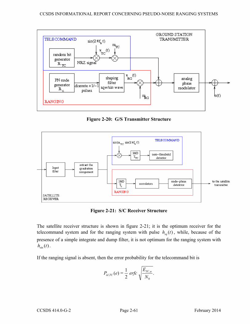
CCSDS INFORMATIONAL REPORT CONCERNING PSEUDO-NOISE RANGING SYSTEMS
CCSDS 414.0-G-2 Page 2-61 February 2014
Figure 2-20: G/S Transmitter Structure
Figure 2-21: S/C Receiver Structure
The satellite receiver structure is shown in figure 2-21; it is the optimum receiver for the telecommand system and for the ranging system with pulse )(thsq , while, because of the presence of a simple integrate and dump filter, it is not optimum for the ranging system with
)(sin th .
If the ranging signal is absent, then the error probability for the telecommand bit is
.21=)(
0
,, N
EerfceP uTC
TCid

CCSDS INFORMATIONAL REPORT CONCERNING PSEUDO-NOISE RANGING SYSTEMS
CCSDS 414.0-G-2 Page 2-62 February 2014
If the ranging signal is present, then the telecommand system suffers from a small loss (see figure 2-22) and )()( , ePeP TCidTC > . Table 2-13 lists the measured loss for
410=)( −ePTC , 0.7=RGm rad and 1.0=TCm rad. The losses shown here and in 2.8.3 were all measured through simulation.
Table 2-13: Uplink Losses for the TC System at PTC(e)=10−4, mTC=1 rad, mRG=0.7 rad
code )(=)( thth sq )(=)( thth sin
T2B 0.04 dB 0.06 dB
T4B 0.02 dB 0.05 dB
Figure 2-22: Input of the TC Zero-Threshold Detector in the Presence of Ranging Interference (No Noise), mTC=1 rad, mRG=0.7rad
As for the ranging system, the case with )(sin th suffers from a loss equal to
∫=π
π 002
0
21
10sin ))sin(sin(1)(,)()(2log10= duuxxE
mEmJL
RG
RG
because of the pulse mismatch in the integrate & dump receiver; this loss amounts to 0.85 dB when mRG=0.7 rad. Moreover, there is a further loss resulting from the interfering telecommand signal. Table 2-14 lists the losses for the ranging system at PRNG(e)=10−6 (i.e., probability that the PN code phase is wrongly estimated), with mTC=1 rad, mRG=0.7. The
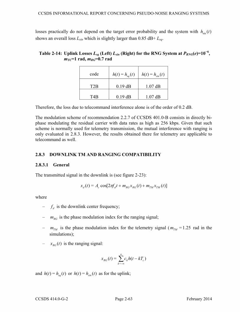
CCSDS INFORMATIONAL REPORT CONCERNING PSEUDO-NOISE RANGING SYSTEMS
CCSDS 414.0-G-2 Page 2-63 February 2014
losses practically do not depend on the target error probability and the system with )(sin th shows an overall loss Lsin which is slightly larger than 0.85 dB+ Lsq.
Table 2-14: Uplink Losses Lsq (Left) Lsin (Right) for the RNG System at PRNG(e)=10−6, mTC=1 rad, mRG=0.7 rad
code )(=)( thth sq )(=)( thth sin
T2B 0.19 dB 1.07 dB
T4B 0.19 dB 1.07 dB
Therefore, the loss due to telecommand interference alone is of the order of 0.2 dB.
The modulation scheme of recommendation 2.2.7 of CCSDS 401.0-B consists in directly bi-phase modulating the residual carrier with data rates as high as 256 kbps. Given that such scheme is normally used for telemetry transmission, the mutual interference with ranging is only evaluated in 2.8.3. However, the results obtained there for telemetry are applicable to telecommand as well.
2.8.3 DOWNLINK TM AND RANGING COMPATIBILITY
2.8.3.1 General
The transmitted signal in the downlink is (see figure 2-23):
)]()([2cos=)( txmtxmtfAtx TMTMRGRGdcd ++π
where
– df is the downlink center frequency;
– RGm is the phase modulation index for the ranging signal;
– TMm is the phase modulation index for the telemetry signal ( 1.25=TMm rad in the simulations);
– )(txRG is the ranging signal:
)(=)(=
ckk
RG kTthctx −∑∞
−∞
and )(=)( thth sq or )(=)( thth sin as for the uplink;

CCSDS INFORMATIONAL REPORT CONCERNING PSEUDO-NOISE RANGING SYSTEMS
CCSDS 414.0-G-2 Page 2-64 February 2014
– )(txTM is the telemetry signal:
)(=)(=
TMTMkk
TM kTtpdtx −∑∞
−∞
and 1=)(tpTM for /2][0, TMTt∈ , 1=)( −tpTM for ]/2,[ TMTM TTt∈ , TMTM RT 1/= is the telemetry symbol interval and TMR is the symbol rate for the telemetry data ( 500=TMR ks/s in the simulations), 1= ±kd is a random sequence.
If the rectangular pulse )(thsq is used for the ranging signal, then the energies used to transmit one ranging chip and one telemetry symbol are, respectively:
cRGTMc
dRG TmmAE ][sin][cos222
2
, = ; TMTMRGc
dTM TmmAE ][sin][cos222
2
, =
while they are
cRGTMc
dRG TmJmAE )(2]2[cos22
12
2
, = ; TMTMRGc
dTM TmmJAE ][sin)(2
220
2
, =
if the sinusoidal pulse )(sin th is used. The G/S receiver is shown in figure 2-24 for a transmitted pulse )(thsq , and in figure 2-25 for a transmitted pulse )(sin th (at the ground station a more complex receiver is feasible).
Figure 2-23: S/C Transmitter Structure

CCSDS INFORMATIONAL REPORT CONCERNING PSEUDO-NOISE RANGING SYSTEMS
CCSDS 414.0-G-2 Page 2-65 February 2014
Figure 2-24: G/S Receiver Structure for Pulse )(thsq
Figure 2-25: G/S Receiver Structure for Pulse )(sin th
2.8.3.2 CTL Tracking Jitter
The quadrature component of the noiseless received signal, used for the detection of telemetry bits and ranging chips and chip clock synchronization is:
)]([cos)]([sin=)( txmtxmAtx TMTMRGRGcq
)]([sin)]([cos txmtxmA TMTMRGRGc+
CCSDS INFORMATIONAL REPORT CONCERNING PSEUDO-NOISE RANGING SYSTEMS
CCSDS 414.0-G-2 Page 2-66 February 2014
and, for )(=)( thth sq (the only case analyzed in this subsection):
)(][sin][cos=)(=
csqkk
RGTMcq kTthcmmAtx −∑∞
−∞
)(][sin][cos=
TMTMkk
TMRGc kTtpdmmA −+ ∑∞
−∞
).()(= ,, txtx TMqRGq +
Since the ranging signal and the telemetry signal are statistically independent the power spectrum of )(txq is simply:
)(])[sin][cos()(])[sin][cos(=)( 22 fGmmAfGmmAfG TMTMRGcRGRGTMcqx + ,
where
22
/2/2)(sin=)( ⎥
⎦
⎤⎢⎣
⎡
TM
TMTMTM fT
fTTfGππ
is the power spectrum of )(= TMTMkk
kTtpd −∑∞
−∞;
)/(||=)( 2
=rk
kRG TkffG −∑
∞
−∞
δν
is the power spectrum of the periodic ranging signal )(= csqkk
kTthc −∑∞
−∞ (period crr TLT = ),
being
,/
)/(sin|)(=|||2
22⎥⎦
⎤⎢⎣
⎡
r
rn Ln
LnnCππν with .1=)( /2
1
0=
rLnkjk
rL
kr
ecL
nC π−−
∑
As far as the chip clock synchronization is concerned, of interest is the power spectrum at frequency rrccRC TLRTf /2)/(=/2=)1/(2= . At this frequency, )( fGRG includes a spectral line with coefficient
2
22/2
2|/2)(=||| ⎥⎦⎤
⎢⎣⎡π
ν rrL LC
and 2|/2)(| rLC is given in table 2-15 for the considered ranging codes (see also table 2-3).
CCSDS INFORMATIONAL REPORT CONCERNING PSEUDO-NOISE RANGING SYSTEMS
CCSDS 414.0-G-2 Page 2-67 February 2014
Table 2-15: Coefficient C(Lr/2) for Codes T2B and T4B
code /2)( rLC 210 |/2)(|log10 rLC
T2B −0.62736 −4.05 dB
T4B −0.9368 −0.55 dB
The power spectrum continuous component )( fGTM at RCf is equal to
22
)/(4))/(4(sin=))(1/(2 ⎥⎦
⎤⎢⎣
⎡
cTM
cTMTMcTM TT
TTTTGππ
Therefore, as far as the chip synchronization is concerned, the ratio between the useful component of the ranging signal and the interference component of the telemetry signal in a bandwidth LB is
22
222
2
))]/(4(sin[)]/(4[2|/2)(|
)(tan)(tan=
TMcLTM
TMcr
TM
RG
RRBTRRLC
mm
ππ
πη ⎥⎦
⎤⎢⎣⎡
⎥⎦
⎤⎢⎣
⎡
Of course, the higher is η , the better is the CTL performance. It is seen that η depends on the ratio )/(4 TMc RR : if 2=cR Mchip/s and 500=TMR kbit/s, then 1=)/(4 TMc RR and
∞→η ; for other values of cR there are finite values of η . The system was therefore analyzed for 2=cR Mchip/s and 1.9=cR Mchip/s. Figure 2-26 shows the CTL transient in the simpler case in which only the clock component of the ranging signal is generated (so that the CTL is the optimum synchronizer and C(Lr/2)=1); the effects of the telemetry signal can be seen as a mean offset with respect to the ideal synchronization time (which corresponds to a mean error in the estimation of the distance, i.e., lack of accuracy), but the offset is present only when the CTL bandwidth is very large. Therefore telemetry interference on the ranging chip synchronization is present, but it can be considered negligible for normal loop bandwidths.

CCSDS INFORMATIONAL REPORT CONCERNING PSEUDO-NOISE RANGING SYSTEMS
CCSDS 414.0-G-2 Page 2-68 February 2014
Figure 2-26: CTL Acquisition Transient, Only Clock Component for the Ranging Signal, mTM=1.25 rad, mRG=0.2 rad, RTM=500 ks/s, Rc=1.9Mc/s
As for the CTL timing jitter (i.e., estimation precision), figures 2-27 and 2-28 show the measured normalized variance 22 / cTεσ for chip rates 2 Mc/s and 1.9 Mc/s. The curve labelled ‘ideal baseband’ is related to the case in which the CTL has an input equal to the clock component plus noise at baseband (no telemetry), so that
)/4/()/4/(/ 0022 NETBNPBT ccLrLc ==εσ (as obtained in 2.5.1). The other curves are related
to the PN ranging codes T2B and T4B interfered by the telemetry signals: the theoretical ranging variance in the absence of telemetry interference is
)/|)2/(|4/()/4/(/ 0,2
022 NELCTBNPBT dRGrcLrLc ==εσ
and therefore a given ranging variance is obtained with a ratio 0, / NE dRG which is 0.55 or 4.05 dB higher than in the ideal case for codes T4B and T2B, respectively. The curves shown in the figures for codes T2B and T4B are shifted by 0.55 and 4.05 dB when the variance is around 10−3, while the shift becomes slightly larger for smaller variances (further loss of about 0.5 dB at 10−5). The extra loss is equal for the two codes. In conclusion, telemetry has a negligible effect on the CTL precision and accuracy.
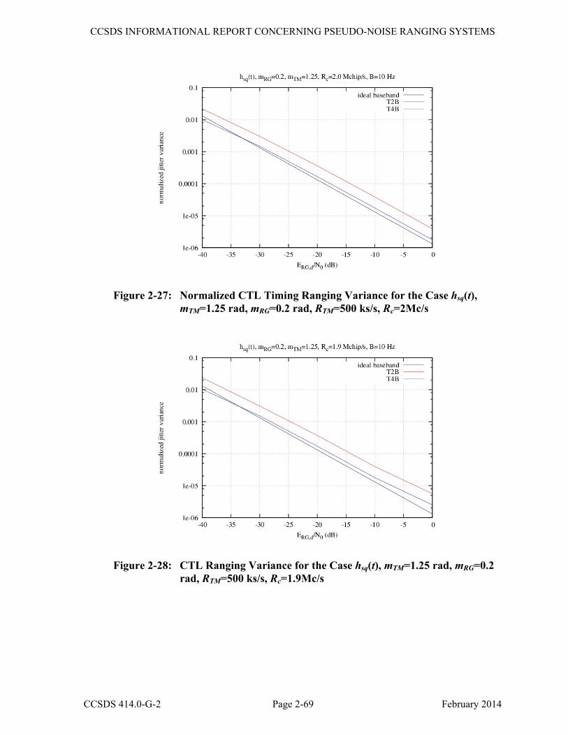
CCSDS INFORMATIONAL REPORT CONCERNING PSEUDO-NOISE RANGING SYSTEMS
CCSDS 414.0-G-2 Page 2-69 February 2014
Figure 2-27: Normalized CTL Timing Ranging Variance for the Case hsq(t), mTM=1.25 rad, mRG=0.2 rad, RTM=500 ks/s, Rc=2Mc/s
Figure 2-28: CTL Ranging Variance for the Case hsq(t), mTM=1.25 rad, mRG=0.2 rad, RTM=500 ks/s, Rc=1.9Mc/s

CCSDS INFORMATIONAL REPORT CONCERNING PSEUDO-NOISE RANGING SYSTEMS
CCSDS 414.0-G-2 Page 2-70 February 2014
2.8.3.3 PN Ranging Acquisition
As for the ranging system, the losses due to the interfering telemetry signal were measured through simulation, and they are given in table 2-16 for the case mTM=1.25 rad, mRG=0.7 rad: code T4B suffers from higher losses and pulse )(thsq is more robust against the interference. Figure 2-29 shows the ranging losses due to the telemetry signal as function of mRG, when mTM=1.25 rad and 2=cR Mchip/s, 500=TMR kbit/s: the loss decreases with mRG, and the best case is that with code T2B and )(thsq . Smaller losses result if telemetry and ranging are not synchronous as is normally the case.
Table 2-16: Downlink Losses Lsq (Left) Lsin (Right) for the RNG System at PRG(e)=10−6, mTM=1.25 rad, mRG=0.7
code )(=)( thth sq )(=)( thth sin
T2B 0.06 dB 0.10 dB
T4B 0.63 dB 1.16 dB
Figure 2-29: Downlink Ranging Losses (dB) with Respect to mRG, for mTM=1.25 rad

CCSDS INFORMATIONAL REPORT CONCERNING PSEUDO-NOISE RANGING SYSTEMS
CCSDS 414.0-G-2 Page 2-71 February 2014
2.8.3.4 TM BER
In the absence of ranging, the telemetry symbol error probability is
0
,, 2
1=)(N
EerfceP dTM
TMid .
Ranging introduces interference, as shown in figure 2-30: in the absence of noise and ranging, the detector input only takes the two values ±0.7, while in the presence of ranging 4 levels appear, and the lowest level in absolute value (i.e., 0.5) is more frequent for code T2B (left) than T4B (right). Table 2-17 lists the losses of the telemetry system at PTM(e)=10−4, mTM=1.25 rad, mRG=0.7, and it is possible to observe that code T4B generates a smaller loss, and that pulse )(sin th produces less interference than pulse )(thsq . Figure 2-31 shows the telemetry losses due to the ranging signal as function of mRG, when mTM=1.25 rad: the loss increases with mRG, and the best case is that with code T4B and )(sin th . Further simulations were run in order to measure the losses when a non-integer ratio exists between the chip rate and the TM symbol rate; figure 2-32 shows the cases of RTM=500 ks/s and Rc=1.7 Mc/s or 1.9 Mc/s: the differences between the cases )(sin th and )(thsq is much reduced, and pulse
)(thsq is now to be preferred, while code T2B again introduces a higher loss on the telemetry system than code T4B. In conclusion, the ranging signal worsens the telemetry system performance and code T2B has a greater impact than code T4B; the measured losses are below 1 dB, but the exact loss depends on the chosen parameters.
Figure 2-30: Samples at the Input of the Zero-Threshold Detector of the Telemetry Receiver; Case of Pulse hsq(t), mTM=1.25 rad, mRG=0.7 rad, Codes T2B (Left) and T4B (Right), No Noise

CCSDS INFORMATIONAL REPORT CONCERNING PSEUDO-NOISE RANGING SYSTEMS
CCSDS 414.0-G-2 Page 2-72 February 2014
Table 2-17: Downlink Losses for the TM System at PTM(e)=10−4, mTM=1.25 rad, mRG=0.7
code )(=)( thth sq )(=)( thth sin
T2B 0.84 dB 0.29 dB
T4B 0.18 dB 0.09 dB
Figure 2-31: Downlink Telemetry Losses (dB) with Respect to mRG, for mTM=1.25 rad
Figure 2-32: Downlink Telemetry Losses (dB) with Respect to mRG, for mTM=1.25
rad, and Chip Rates 1.9 Mc/s and 1.7 Mc/s
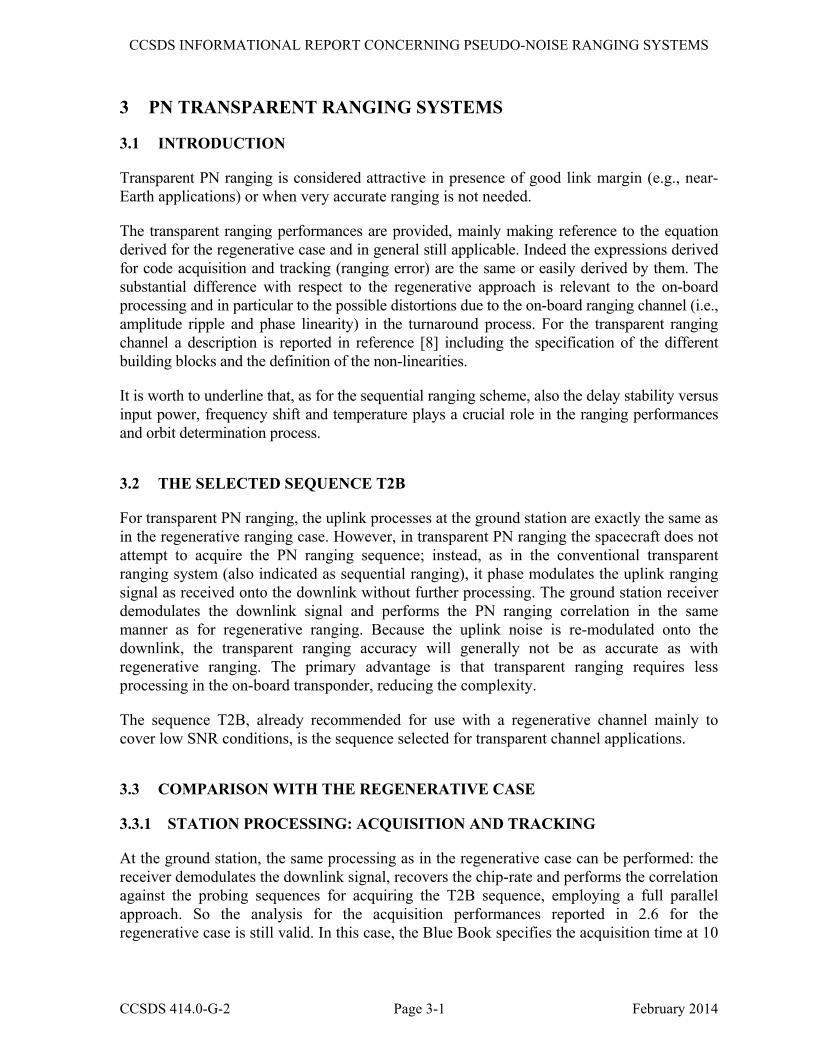
CCSDS INFORMATIONAL REPORT CONCERNING PSEUDO-NOISE RANGING SYSTEMS
CCSDS 414.0-G-2 Page 3-1 February 2014
3 PN TRANSPARENT RANGING SYSTEMS
3.1 INTRODUCTION
Transparent PN ranging is considered attractive in presence of good link margin (e.g., near-Earth applications) or when very accurate ranging is not needed.
The transparent ranging performances are provided, mainly making reference to the equation derived for the regenerative case and in general still applicable. Indeed the expressions derived for code acquisition and tracking (ranging error) are the same or easily derived by them. The substantial difference with respect to the regenerative approach is relevant to the on-board processing and in particular to the possible distortions due to the on-board ranging channel (i.e., amplitude ripple and phase linearity) in the turnaround process. For the transparent ranging channel a description is reported in reference [8] including the specification of the different building blocks and the definition of the non-linearities.
It is worth to underline that, as for the sequential ranging scheme, also the delay stability versus input power, frequency shift and temperature plays a crucial role in the ranging performances and orbit determination process.
3.2 THE SELECTED SEQUENCE T2B
For transparent PN ranging, the uplink processes at the ground station are exactly the same as in the regenerative ranging case. However, in transparent PN ranging the spacecraft does not attempt to acquire the PN ranging sequence; instead, as in the conventional transparent ranging system (also indicated as sequential ranging), it phase modulates the uplink ranging signal as received onto the downlink without further processing. The ground station receiver demodulates the downlink signal and performs the PN ranging correlation in the same manner as for regenerative ranging. Because the uplink noise is re-modulated onto the downlink, the transparent ranging accuracy will generally not be as accurate as with regenerative ranging. The primary advantage is that transparent ranging requires less processing in the on-board transponder, reducing the complexity.
The sequence T2B, already recommended for use with a regenerative channel mainly to cover low SNR conditions, is the sequence selected for transparent channel applications.
3.3 COMPARISON WITH THE REGENERATIVE CASE
3.3.1 STATION PROCESSING: ACQUISITION AND TRACKING
At the ground station, the same processing as in the regenerative case can be performed: the receiver demodulates the downlink signal, recovers the chip-rate and performs the correlation against the probing sequences for acquiring the T2B sequence, employing a full parallel approach. So the analysis for the acquisition performances reported in 2.6 for the regenerative case is still valid. In this case, the Blue Book specifies the acquisition time at 10

CCSDS INFORMATIONAL REPORT CONCERNING PSEUDO-NOISE RANGING SYSTEMS
CCSDS 414.0-G-2 Page 3-2 February 2014
dBHz, which gives a theoretical acquisition time of 26.2 s, which is a factor of 100 larger than the transparent case.
Also the tracking performances (in terms of jitter) can be derived from the same expressions evaluated for the regenerative ranging. In particular for the closed loop case (based on CTL) the analysis reported in 2.5 is still valid, while for the open loop architecture the results of 2.7.2 are applicable. Of course the end-to-end performances analysis of 2.7.3 is not applicable anymore since the on-board contribution to the tracking jitter disappears. Table 3-1 show the result with the same conditions indicated in the Blue Book (reference [1]):
– BL=0.1 Hz (or T=5 s);
– Chip rate Fc = 2.068 Mchip/s; fRC= Fc/2;
– PR/N0 =10 dBHz.
Table 3-1: Station Ranging Jitter Performances
Sequence sq_sine__ CTLRangeσ sine_sine__ OLRangeσ
T2B 4.1 m 3.7 m
It is worth to underline that the above results for station acquisition and performances are based on theoretical evaluations assuming an ideal on-board turnaround operation (with no impacts due to non-linearity).
3.3.2 ON-BOARD PROCESSING
The theoretical acquisition performances derived in the previous subsection and obtained using the same equations derived for the regenerative case can be affected by the impacts due to the on-board ranging processing, in particular in-band ripple and phase linearity. Analysis was done in order to define requirements for:
– the channel non-linearities (in-band group delay variations and gain flatness);
– the 3 dB bandwidth;
– and the noise bandwidth.
The analysis is performed in a parametric way considering:
– different high cut-off frequencies;
– the presence or not of a TC echo rejection filter (low cut-off frequency).
It is shown in references [8], [11], and [12] that:
CCSDS INFORMATIONAL REPORT CONCERNING PSEUDO-NOISE RANGING SYSTEMS
CCSDS 414.0-G-2 Page 3-3 February 2014
– A pure low-pass channel offers better acquisition performances compared to a channel with a high pass filter to remove the TC.
– In case of a high pass filter with cut-off at around 350 kHz, calculated acquisition times for Fc = 3 Mchip/s increased by about 50%. At very low PR/N0, the effect is that the acquisition time becomes impractically long.
– To keep the on-ground PN sequence acquisition close to the theoretical value, a wideband channel is desirable.
– The one-sided bandwidth has to be at least 1.5*Fc wide for a maximum 10% increase of acquisition time.

CCSDS INFORMATIONAL REPORT CONCERNING PSEUDO-NOISE RANGING SYSTEMS
CCSDS 414.0-G-2 Page 4-1 February 2014
4 PN RANGING VIA NON-COHERENT TRANSPONDERS
4.1 GENERAL
For missions that desire to range using a transceiver or a non-coherent transponder and do not require high accuracy ranging, it is possible to perform two-way non-coherent ranging. This technique has the advantage that it can allow for simpler hardware onboard the spacecraft. It can be applied to either transparent or regenerative ranging.
With two-way non-coherent ranging, the on-board processing of the uplink signal is identical to the coherent ranging described in previous subsections. The spacecraft either phase modulates the noisy received uplink PN ranging signal onto the downlink carrier (in the transparent ranging case), or acquires the PN ranging sequence and regenerates the uplink ranging signal as described in 2.4 (in the regenerative ranging case). However, because the downlink carrier frequency is referenced to an onboard oscillator rather than the uplink carrier, the ground station will not be able to perform carrier Doppler pre-steering of the ranging signal. This is because the received chip rate has Doppler contributions from both the uplink and downlink, while the received carrier frequency only has Doppler contribution from the downlink plus a frequency error component due to the onboard oscillator. Doppler pre-steering requires that the received carrier Doppler and chip rate Doppler be matched.
When using non-coherent ranging and an open loop receiver at the station, there will generally be a chip rate mismatch between the received PN code and the local model correlated against at the ground station. This is due to uncompensated Doppler. The difference in the chip rates will cause the ranging correlation to be degraded, and introduce a range bias in the measurement. If the spacecraft trajectory is well known, then the uplink frequency and chip rate can be adjusted to minimize the Doppler seen at the spacecraft.
Additionally, there is also a chip rate mismatch due to the spacecraft oscillator frequency error component. This can be mitigated, but in general not entirely removed, by adjusting the uplink frequency and chip rate to compensate for the spacecraft oscillator frequency drift in addition to the uplink Doppler. Another solution would be to use a Ultra-Stable Oscillator (USO) as a reference for the downlink carrier and PN chip rate onboard the spacecraft.
4.2 GROUND STATION OPEN LOOP RECEIVER
For the open loop model of the ground station receiver, the range clock mismatch between the received PN code and the local model has two primary effects. The first effect is a reduction in correlation amplitude, which in turn reduces the ranging SNR and makes the range measurement noisier. The reduction in correlation amplitude, Ac, is given by reference [3]:
TfTf
Achip
chipc Δ
Δ=
ππ )sin(
CCSDS INFORMATIONAL REPORT CONCERNING PSEUDO-NOISE RANGING SYSTEMS
CCSDS 414.0-G-2 Page 4-2 February 2014
where Δfchip is the frequency difference between the received chip rate and the local model (the chip rate is twice the range clock frequency), and T is the integration time. The reduction in correlation amplitude reduces the ranging SNR and increases the jitter due to thermal noise and the acquisition time.
The second effect is a range bias introduced because of the frequency mismatch. The difference in frequency between the local model and the received range clock causes the phase difference between them to drift during the measurement interval. Provided that the range measurement is referenced to the start of the integration interval instead of the middle, the range error is equal to one-half the total drift during the integration time, T, as follows reference [3]:
chip
chip
fTfc
biasRange4Δ
=
where Δfchip is the difference in frequency between the received chip rate and the local chip rate. The frequency error will in general have contributions due to both spacecraft oscillator frequency drift and imperfect uplink Doppler predicts. The range bias error is proportional to the integration time for a given chip rate difference. Thus for non-coherent ranging measurements, it is preferable to use the shortest integration time allowed by the thermal noise constraint.
4.3 GROUND STATION CLOSED-LOOP RECEIVER
For the closed-loop model of the ground station ranging receiver, the CTL bandwidth must be made wide enough to track the changes in chip rate caused by on-board oscillator drift and uncompensated Doppler. This will limit the jitter performance as described by equations in 2.7 (for the regenerative case) and 3.3 (for the transparent ranging case). In addition, there will be a range bias as described by the equation in the previous subsection.

CCSDS INFORMATIONAL REPORT CONCERNING PSEUDO-NOISE RANGING SYSTEMS
CCSDS 414.0-G-2 Page 5-1 February 2014
5 OCCUPIED BANDWIDTH CONSIDERATIONS
Theoretical analysis, simulations and measurements have been done in the frame of the BepiColombo mission that selected this PN ranging techniques for use at 7, 8, 32 and 34 GHz with large modulation indexes assigned to the ranging signal.
Table 5-1 below presents the obtained measurements of the ITU 99% power bandwidth (the bandwidth that contains 99% of the total power) for three representative values of the ranging modulation index, and for both T2B and T4B codes.
The column “unfiltered bandwidth” is the bandwidth obtained by modulating the squarewave ranging signal directly on the carrier whereas the column “sinewave” is obtained with the sinewaving shaping specified in 2.3.1. The values given are normalized to the chip rate. For a modulation index of 1.0 rad and 1 Mchip/s, the use of unfiltered T4B code results in an occupied bandwidth of 27 MHz which is extremely wide. The whole deep space allocation at 7 GHz is 45 MHz wide!
The use of sinewave shaping in the same conditions results in only 2 MHz of bandwidth. This major difference is due to the rich harmonic contents of squarewaves that play an increasingly significant role for higher modulation indexes.
Table 5-1: Normalized Occupied Bandwidth Values
Code 99% BW
unfiltered squarewave
99% BW
filtered squarewave
99% BW
sinewave
m
(rad)
T2B 3.0 2.5 1.0 0.3 11.6 7.1 2.0 0.7 20.9 10.0 2.0 1.0
T4B 3.0 3.0 1.0 0.3 15.0 7.0 1.5 0.7 27.0 10.0 2.0 1.0
For modulation indexes of 0.3 rad or below, the difference between sinewave and squarewave is not so large and the latter may be acceptable. Squarewave shaping may also be acceptable for chip rates below 250 kchip/s with modulation indexes below 1.0 rad.