PSCAD modeling of a two-level space vector pulse width ... · PSCAD includes comprehensive library...
15
Available online at www.sciencedirect.com ScienceDirect Journal of Electrical Systems and Information Technology 3 (2016) 333–347 PSCAD modeling of a two-level space vector pulse width modulation algorithm for power electronics education Ahmet Mete Vural Electrical and Electronics Engineering Department, University of Gaziantep, 27310 S ¸ehitkamil, Gaziantep, Turkey Received 21 October 2015; received in revised form 7 January 2016; accepted 24 January 2016 Available online 4 August 2016 Abstract This paper presents the design details of a two-level space vector pulse width modulation algorithm in PSCAD that is able to generate pulses for three-phase two-level DC/AC converters with two different switching patterns. The presented FORTRAN code is generic and can be easily modified to meet many other kinds of space vector modulation strategies. The code is also editable for hardware programming. The new component is tested and verified by comparing its output as six gating signals with those of a similar component in MATLAB library. Moreover the component is used to generate digital signals for closed-loop control of STATCOM for reactive power compensation in PSCAD. This add-on can be an effective tool to give students better understanding of the space vector modulation algorithm for different control tasks in power electronics area, and can motivate them for learning. © 2016 Electronics Research Institute (ERI). Production and hosting by Elsevier B.V. This is an open access article under the CC BY-NC-ND license (http://creativecommons.org/licenses/by-nc-nd/4.0/). Keywords: Space vector pulse width modulation; Simulation model; Voltage source inverter; Power electronics; Graduate education 1. Introduction The conversion of electrical power from one form into another and its control have always been live research topics that can be implemented with various power electronic circuit topologies (Rashid, 2013). Among these, force- commutated voltage source inverters (VSIs) with different topologies, ranging from different voltage and power levels, can synthesize variable AC voltage and frequency from a fixed DC voltage source efficiently to convert a DC voltage to an AC, sinusoidal, three-phase voltage of controllable frequency, phase angle, and amplitude (Colak et al., 2011). Space vector pulse width modulation (SVPWM) is an industry accepted algorithm for up-to-date VSIs beside the widely used E-mail addresses: [email protected], [email protected] Peer review under the responsibility of Electronics Research Institute (ERI). http://dx.doi.org/10.1016/j.jesit.2016.01.005 2314-7172/© 2016 Electronics Research Institute (ERI). Production and hosting by Elsevier B.V. This is an open access article under the CC BY-NC-ND license (http://creativecommons.org/licenses/by-nc-nd/4.0/).
Transcript of PSCAD modeling of a two-level space vector pulse width ... · PSCAD includes comprehensive library...
A
gifaSo©B
K
1
tccav
2B
Available online at www.sciencedirect.com
ScienceDirect
Journal of Electrical Systems and Information Technology 3 (2016) 333–347
PSCAD modeling of a two-level space vector pulse widthmodulation algorithm for power electronics education
Ahmet Mete VuralElectrical and Electronics Engineering Department, University of Gaziantep, 27310 Sehitkamil, Gaziantep, Turkey
Received 21 October 2015; received in revised form 7 January 2016; accepted 24 January 2016Available online 4 August 2016
bstract
This paper presents the design details of a two-level space vector pulse width modulation algorithm in PSCAD that is able toenerate pulses for three-phase two-level DC/AC converters with two different switching patterns. The presented FORTRAN codes generic and can be easily modified to meet many other kinds of space vector modulation strategies. The code is also editableor hardware programming. The new component is tested and verified by comparing its output as six gating signals with those of
similar component in MATLAB library. Moreover the component is used to generate digital signals for closed-loop control ofTATCOM for reactive power compensation in PSCAD. This add-on can be an effective tool to give students better understandingf the space vector modulation algorithm for different control tasks in power electronics area, and can motivate them for learning.
2016 Electronics Research Institute (ERI). Production and hosting by Elsevier B.V. This is an open access article under the CCY-NC-ND license (http://creativecommons.org/licenses/by-nc-nd/4.0/).
eywords: Space vector pulse width modulation; Simulation model; Voltage source inverter; Power electronics; Graduate education
. Introduction
The conversion of electrical power from one form into another and its control have always been live researchopics that can be implemented with various power electronic circuit topologies (Rashid, 2013). Among these, force-ommutated voltage source inverters (VSIs) with different topologies, ranging from different voltage and power levels,
an synthesize variable AC voltage and frequency from a fixed DC voltage source efficiently to convert a DC voltage ton AC, sinusoidal, three-phase voltage of controllable frequency, phase angle, and amplitude (Colak et al., 2011). Spaceector pulse width modulation (SVPWM) is an industry accepted algorithm for up-to-date VSIs beside the widely usedE-mail addresses: [email protected], [email protected] review under the responsibility of Electronics Research Institute (ERI).
http://dx.doi.org/10.1016/j.jesit.2016.01.005314-7172/© 2016 Electronics Research Institute (ERI). Production and hosting by Elsevier B.V. This is an open access article under the CCY-NC-ND license (http://creativecommons.org/licenses/by-nc-nd/4.0/).
334 A.M. Vural / Journal of Electrical Systems and Information Technology 3 (2016) 333–347
carrier based pulse-width modulation, in which a triangular carrier signal is compared to a reference waveform, usuallyin the form of pure sinusoidal, sinusoidal plus third harmonic component, or a trapezoidal waveform to obtain theappropriate firing pulses to each of the bidirectional switches. The main benefits of the SVPWM when compared tothe carrier based modulation approaches are (Valan Rajkumar and Manoharan, 2013; Holmes and Lipo, 2003a): higherDC voltage utilization with 15%, less total harmonic distortion (THD), and reduction in switching loss (Stumpf et al.,2013). But the disadvantage of SVPWM is that it requires complex online computation (Durgasukumar and Pathak,2012). There are variations of SVPWM that result in different quality and computational requirements (Chen et al.,2013; Huang et al., 2012). SVPWM strategies are broadly applied in the open literature to variable frequency drives(Lu and Qu, 2007; Vafakhah and Salmon, 2010; Ün and Hava, 2009), active power filters (Asiminoaei and Rodriguez,2008a,b; Demirkutlu and Hava, 2009; Xiang et al., 2011), renewable energy systems (Valan Rajkumar and Manoharan,2013; Valan Rajkumar et al., 2013; Karimi-Davijani et al., 2008), and FACTS/HVDC applications (Wang and Cathey,2003; Geethalakshmi and Dananjayan, 2008; Norouzizadeh et al., 2010; Xiao et al., 2011; Omar and Rahim, 2009;Xiaojie and Yi, 2011).
Perhaps, due to the complexity in experimental set-up and hardware programming, the study of VSI applications isusually performed on dynamic simulations, which is more practical and economical than the studies on an experimentalprototype. Moreover, simulation models generally give quick and accurate results with shorter time of design for teach-ing or research purposes. On the other hand, laboratory facilities associated to certain power courses in undergraduateengineering curricula are getting smaller due to the budget constraints (Costa et al., 2012). Dynamic simulation studiesmay also be preferred to be an initial phase of hardware programming for SVPWM based algorithms.
In the last decade increasing attention has been given to VSI control based on SVPWM algorithm for differentcontrol purposes in power systems. In Muyeen et al. (2007), the application of SVPWM technique is presented usingPSCAD standard library components. Although the model is graphically well-described, the chosen parameters of thelibrary components are not provided which makes it difficult to understand the algorithm in full. In Liu et al. (2010), acustom two-level SVPWM component in PSCAD is prepared. Although the theory of the algorithm and the flowchartof the program are given, the script of the custom component is not provided. In Xiang et al. (2011), a three-levelVSI based active filter is controlled using a simplified version of SVPWM in PSCAD, but the implementation ofthe modified algorithm is not clearly stated. In Xiao et al. (2011), a VSC-HVDC system is established in PSCADand validated through case studies. The efficiency of the converters is indirectly increased with the high DC voltageutilization property of the SVPWM algorithm. But the implementation details of the SVPWM algorithm is not provided.In Omar and Rahim (2009), the modeling and simulation of a dynamic voltage restorer to mitigate voltage sags ispresented in PSCAD. SVPWM algorithm produces the switching signals of the converter, but its modeling details arenot given in the paper. In Karimi-Davijani et al. (2008), a black box model of the SVPWM is provided that controlsthe two converters of a doubly fed induction generator for wind turbine application. Xiaojie and Yi (2011) describethe modeling and analysis of a three-level STATCOM based on SVPWM without presenting the modeling details. Thecommon observed situation in the above works and in the open literature is that although the SVPWM algorithm issuccessfully applied to the control of the VSIs, the papers mainly focus on the transient performance of the controlsystem rather than the SVPWM algorithm itself.
The author is aware of the fact that the older versions of PSCAD (v4.2, v4.3) do not include SVPWM componentand only the two recent versions of PSCAD (v4.4, v4.5) include a standard SVPWM component in the master library.Unfortunately the available model is not open-source and does not provide full FORTRAN code for customization(Monitoba Hydro). In this paper, two variations of SVPWM algorithm that result in different harmonic quality andcomputational requirements are fully presented. Moreover, SVPWM algorithm is applied for the pulse generation ofa two-level STATCOM for model verification. The presented SVPWM algorithm is open and extendable, which ishighly suitable for power electronics education/research.
2. Principle of SVPWM
The theory of SVPWM is well known and well documented in the literature (Holmes, 1996; Holtz, 1992; Holmes
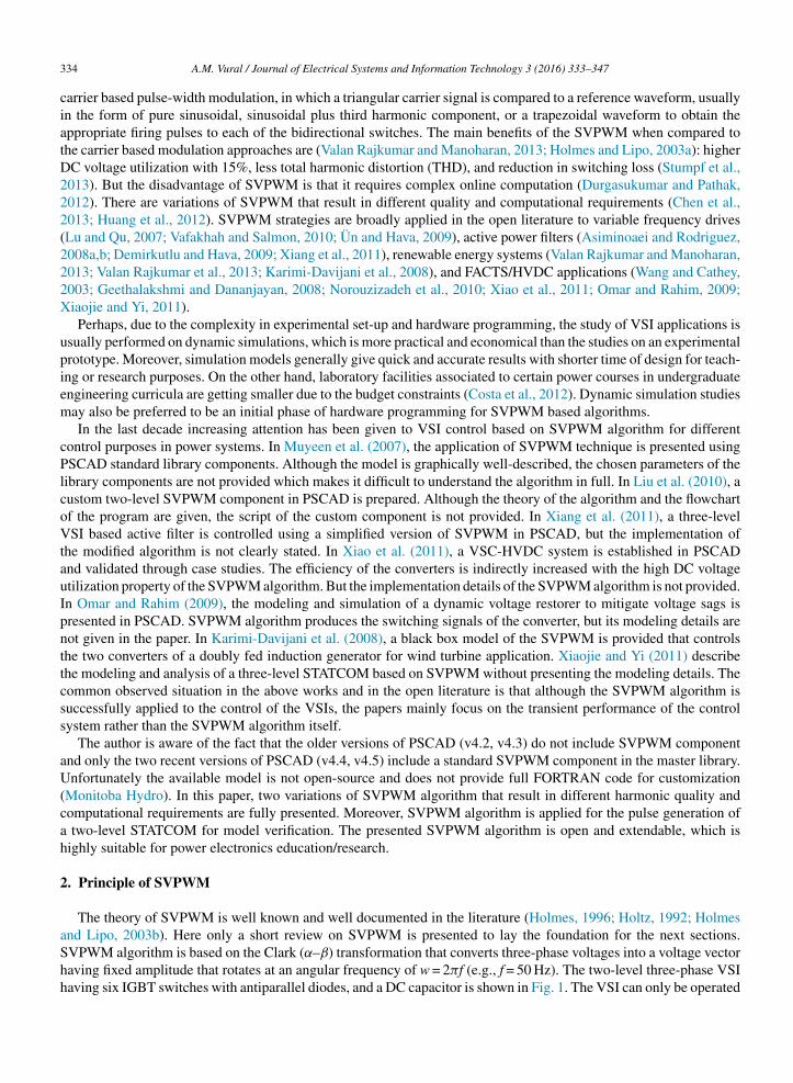
and Lipo, 2003b). Here only a short review on SVPWM is presented to lay the foundation for the next sections.SVPWM algorithm is based on the Clark (α–β) transformation that converts three-phase voltages into a voltage vectorhaving fixed amplitude that rotates at an angular frequency of w = 2πf (e.g., f = 50 Hz). The two-level three-phase VSIhaving six IGBT switches with antiparallel diodes, and a DC capacitor is shown in Fig. 1. The VSI can only be operated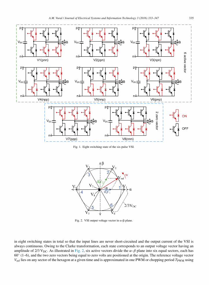
A.M. Vural / Journal of Electrical Systems and Information Technology 3 (2016) 333–347 335
Fig. 1. Eight switching state of the six-pulse VSI.
Fig. 2. VSI output voltage vector in �-� plane.
iaa6V
n eight switching states in total so that the input lines are never short-circuited and the output current of the VSI is
lways continuous. Owing to the Clarke transformation, each state corresponds to an output voltage vector having anmplitude of 2/3 VDC. As illustrated in Fig. 2, six active vectors divide the α–β plane into six equal sectors, each has0◦ (1–6), and the two zero vectors being equal to zero volts are positioned at the origin. The reference voltage vectorref lies on any sector of the hexagon at a given time and is approximated in one PWM or chopping period TPWM using
336 A.M. Vural / Journal of Electrical Systems and Information Technology 3 (2016) 333–347
a combination of the two adjacent active vectors in the projected sector and one zero vector (Holmes and Lipo, 2003a).For example if Vref is in sector 1, it can be approximated by the summation of two adjacent active vectors (V1, V2), asgiven in Eq. (1), where da and db are the duty cycles of V1 and V2, respectively. The duty cycle of the zero vector, d0,can be calculated as given in Eq. (2). The duty cycle is the duration time for the related switching state, which producesthe related voltage vector at the output. The duty cycle is generally expressed as per unit of TPWM so that d = T/TPWMwhere T is the time-share of the current switching state. Although zero vectors have no direct effect on the synthesisof Vref, they are used in SVPWM algorithm to reduce harmonics, output ripples, and THD (Rashid, 2013; Holmes andLipo, 2003a; Huang et al., 2012).
Vref = daV1 + dbV2 (1)
d0 = 1 − da − db (2)
3. Coding of SVPWM algorithm
PSCAD includes comprehensive library of system models covering many passive elements and control functionsfor studying the transient behavior of electrical apparatus and networks (Monitoba Hydro). It is also very flexiblein building user-defined models. A free version of PSCAD is available for students who wish to model and analyzecustom written algorithms such as SVPWM. This section presents the overall PSCAD model of the SVPWM algorithmincluding its graphical view and flow chart. Besides the full FORTRAN code is provided in Appendix A. Center-alignedsymmetrical switching patterns for SVPWM can be classified according to the distribution style and the realizationmeans of the zero vector. For example, switching states of ppp and nnn can be combined within each single switchingcycle. Or alternatively, switching state ppp can be considered for some of the full switching cycles, while switchingstate nnn is considered for the subsequent full switching cycles. With this respect, the user is able to choose these twotypes of the switching patterns, namely, pattern #1 and pattern #2 (Yu, 2016). Using PSCAD new component wizard,the custom component for SVPWM algorithm is designed as in Fig. 3 which consists of three parts: (i) Graphic, (ii)Parameters, (iii) Script. Graphical part is shown in Fig. 3(a) which has four inputs and one six-dimensional output,each of which is assigned for one IGBT gate to turn it on or off. The “Parameters” part is designed as in Fig. 3(b) thatcan be reached when double clicked on the graphic. It includes one radio button and one drop list to allow the user toselect PLL type and switching pattern type, respectively. “m” is the modulation index input to control the magnitudeof the VSI output voltage either in the under-modulation (0 ≤ m < 0.907) or over-modulation region (0.907 ≤ m ≤ 1)(Bose, 2002). “PLL signal” is the phase locked loop (PLL) input having two options. When “Internal PLL” is selected,the component produces a saw tooth signal with the fundamental frequency (i.e., 50 or 60 Hz), (Fig. 3(c)), specified bythe user with “Fund freq” input. The “PLL signal” input port is then used to set the required phase shift to the saw toothwaveform. FORTRAN does not include a standard command for saw tooth waveform generation so that the waveformis produced by the following function in the range −1 to 1, where t is simulation time and a is period (Wikipedia):
f (t) = 2
(t
a− int
(1
2+ t
a
))(3)
int(x) function returns the largest integer which is not greater than x (e.g., int(2.4) = int(2.7) = 2). The internal PLLsignal is used to simulate the algorithm virtually by incrementing the sector number (1–6) for testing purposes. It isprogrammed that when “PLL signal” is set to zero, the reference voltage vector Vref is aligned on the α-axis (Fig. 2)at time t = 0 and begins to rotate in counter clock wise direction once the model is run. When “External PLL” ischosen, the component accepts the PLL signal from outside so that VSI output voltage can be synchronized with athree-phase reference voltage and closed-loop control of VSI can be made, such as in STATCOM or in active powerfilter applications. The “PWM freq” is the input to set the frequency of two periodic waveforms, saw tooth waveform forpattern #1 and triangular waveform for pattern #2, both are used to determine the switching intervals of the active/zerovectors in one switching period. Sector finding is a prerequisite for both pattern #1 and #2, which finds the projectionof voltage vector on the α–β plane on the execution time. A typical sector distribution may be obtained as in Fig. 3(d)
over time if internal “PLL signal” is set to zero. The sector number is used to calculate the timing of active/zero vectorsin pattern #1, and to execute the conversion table in pattern #2, respectively. The full Fortran code of pattern #1 and#2, are given in Appendix A, including optimum switching sequences for both patterns. Fig. 4 shows how switchingintervals of active and zero vectors are determined for pattern #1 at a switching frequency of 10 kHz. In Fig. 4, Ta,
A.M. Vural / Journal of Electrical Systems and Information Technology 3 (2016) 333–347 337
Fig. 3. SVPWM algorithm implementation in PSCAD.
TibepIsa#oa
b, and T0 represent the application durations of the active and the zero vectors, respectively. For example, if Vref isn sector 1, the subscripts a and b becomes 1 and 2, respectively. For pattern #1, the switching sequence is obtainedy comparing the saw tooth signal with the vector transition time to define the interval (1–7). Later on, the algorithmvaluates the interval and the sector number together to find the optimum switching combination in one switchingeriod. For comparison, the switching signals of pattern #2 in one switching period are given in Fig. 5. Note that eachGBT switches twice per every switching period in pattern #1, while one IGBT remains in the ON-state for the entirewitching period in pattern #2. Consequently, the number of switching times for this pattern is less than pattern #1. As
result, switching losses are reduced with pattern #2. When viewed from the conduction losses point of view, pattern1 has the advantage of equal heating of the six semiconductors due to the realization of zero vector by equal applyingf ppp and nnn zero vectors. However this situation is not the case of pattern #2, in which unequal applying of pppnd nnn zero vectors exist.

338 A.M. Vural / Journal of Electrical Systems and Information Technology 3 (2016) 333–347
Fig. 4. Determination of switching instants of pattern #1 for a switching frequency of 10 kHz.
Fig. 5. Switching signals of pattern #2 in one switching period.

A.M. Vural / Journal of Electrical Systems and Information Technology 3 (2016) 333–347 339
Fig. 6. Test case in PSCAD.
4
wbs
4
V
. Test cases
In this section, the SVPWM algorithm written in PSCAD is tested and verified through various simulation scenarioshen solution time step is set to 2 �s. The simulation model is depicted in Fig. 6 that has a flexible structure using circuitreakers so that two different types of simulation scenarios can be considered which are mentioned in the followingub-sections.
.1. VSI open-loop control
In this case study, SVPWM algorithm which produces the firing pulses to the IGBTs in the two-level six-pulseSI is investigated in open-loop conditions without any feedback measurement. So only the “Power Circuit”, “Gat-

340 A.M. Vural / Journal of Electrical Systems and Information Technology 3 (2016) 333–347
Fig. 7. VSI voltage waveforms and upper-leg gating signals in open-loop conditions.
ing Signal Generation”, and “THD and RMS Measurement” blocks presented in Fig. 6 are used. To observe thesimulated waveforms, AC side and DC side terminals of the VSI is connected to a three-phase resistive load anda DC voltage source, respectively, by turning on the breaker 1. At the same time, VSI should be isolated from thethree-phase source by turning off the breaker 2. This circuit configuration yields a clean waveform observation thatthe VSI produces at its AC terminals when it is fed from a pure DC voltage source without any ripples. The fun-damental and the switching frequency of the SVPWM block is set to 50 Hz and 15 kHz, respectively. When thebreaker 1 is closed, the PSCAD signal “BRK1” becomes 0 so that the inputs “m” and “PLL signal” of the SVPWMblock are set to 0.7 and 0, respectively and the VSI operates in open-loop conditions that produces a three-phasebalanced voltage waveform with a fixed magnitude and zero phase shift according to the internally generated PLL
saw tooth signal. In Fig. 7(a), the line-to-neutral voltage (VAn), the line-to-line voltage (VAB), and upper leg gat-ing signals of the VSI (g1-3) are shown for a duration of two fundamental cycles when pattern #1 is applied. Thesame sort of simulated waveforms are presented in Fig. 7(b) for pattern #2. It is observed that the voltage wave-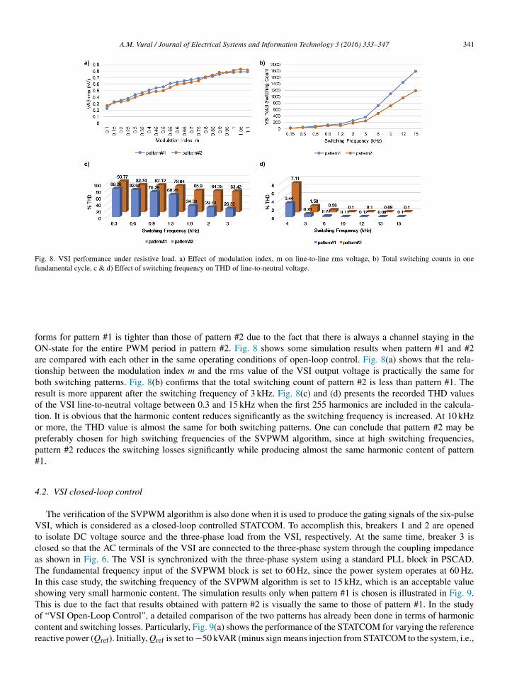
A.M. Vural / Journal of Electrical Systems and Information Technology 3 (2016) 333–347 341
Fig. 8. VSI performance under resistive load. a) Effect of modulation index, m on line-to-line rms voltage, b) Total switching counts in onefundamental cycle, c & d) Effect of switching frequency on THD of line-to-neutral voltage.
fOatbrotopp#
4
VtcaTIsTocr
orms for pattern #1 is tighter than those of pattern #2 due to the fact that there is always a channel staying in theN-state for the entire PWM period in pattern #2. Fig. 8 shows some simulation results when pattern #1 and #2
re compared with each other in the same operating conditions of open-loop control. Fig. 8(a) shows that the rela-ionship between the modulation index m and the rms value of the VSI output voltage is practically the same foroth switching patterns. Fig. 8(b) confirms that the total switching count of pattern #2 is less than pattern #1. Theesult is more apparent after the switching frequency of 3 kHz. Fig. 8(c) and (d) presents the recorded THD valuesf the VSI line-to-neutral voltage between 0.3 and 15 kHz when the first 255 harmonics are included in the calcula-ion. It is obvious that the harmonic content reduces significantly as the switching frequency is increased. At 10 kHzr more, the THD value is almost the same for both switching patterns. One can conclude that pattern #2 may bereferably chosen for high switching frequencies of the SVPWM algorithm, since at high switching frequencies,attern #2 reduces the switching losses significantly while producing almost the same harmonic content of pattern1.
.2. VSI closed-loop control
The verification of the SVPWM algorithm is also done when it is used to produce the gating signals of the six-pulseSI, which is considered as a closed-loop controlled STATCOM. To accomplish this, breakers 1 and 2 are opened
o isolate DC voltage source and the three-phase load from the VSI, respectively. At the same time, breaker 3 islosed so that the AC terminals of the VSI are connected to the three-phase system through the coupling impedances shown in Fig. 6. The VSI is synchronized with the three-phase system using a standard PLL block in PSCAD.he fundamental frequency input of the SVPWM block is set to 60 Hz, since the power system operates at 60 Hz.
n this case study, the switching frequency of the SVPWM algorithm is set to 15 kHz, which is an acceptable valuehowing very small harmonic content. The simulation results only when pattern #1 is chosen is illustrated in Fig. 9.
his is due to the fact that results obtained with pattern #2 is visually the same to those of pattern #1. In the studyf “VSI Open-Loop Control”, a detailed comparison of the two patterns has already been done in terms of harmonicontent and switching losses. Particularly, Fig. 9(a) shows the performance of the STATCOM for varying the referenceeactive power (Qref). Initially, Qref is set to −50 kVAR (minus sign means injection from STATCOM to the system, i.e.,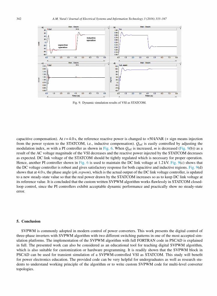
342 A.M. Vural / Journal of Electrical Systems and Information Technology 3 (2016) 333–347
Fig. 9. Dynamic simulation results of VSI as STATCOM.
capacitive compensation). At t = 4.0 s, the reference reactive power is changed to +50 kVAR (+ sign means injectionfrom the power system to the STATCOM, i.e., inductive compensation). Qref is easily controlled by adjusting themodulation index, m with a PI controller as shown in Fig. 6. When Qref is increased, m is decreased (Fig. 9(b)) as aresult of the AC voltage magnitude of the VSI decreases and the reactive power injected by the STATCOM decreasesas expected. DC link voltage of the STATCOM should be tightly regulated which is necessary for proper operation.Hence, another PI controller shown in Fig. 6 is used to maintain the DC link voltage at 1.2 kV. Fig. 9(c) shows thatthe DC voltage controller is robust and gives satisfactory response for both capacitive and inductive regions. Fig. 9(d)shows that at 4.0 s, the phase angle (ph svpwm), which is the actual output of the DC link voltage controller, is updatedto a new steady-state value so that the real power drawn by the STATCOM increases so as to keep DC link voltage atits reference value. It is concluded that the custom written SVPWM algorithm works flawlessly in STATCOM closed-loop control, since the PI controllers exhibit acceptable dynamic performance and practically show no steady-stateerror.
5. Conclusion
SVPWM is commonly adopted in modern control of power converters. This work presents the digital control ofthree-phase inverters with SVPWM algorithm with two different switching patterns in one of the most accepted sim-ulation platforms. The implementation of the SVPWM algorithm with full FORTRAN code in PSCAD is explainedin full. The presented work can also be considered as an educational tool for teaching digital SVPWM algorithm,which is also suitable for customization or hardware programming. It is readily shown that the SVPWM block inPSCAD can be used for transient simulation of a SVPWM-controlled VSI as STATCOM. This study will benefitfor power electronics education. The provided code can be very helpful for undergraduates as well as research stu-dents to understand working principle of the algorithm or to write custom SVPWM code for multi-level convertertopologies.
A
T
A.M. Vural / Journal of Electrical Systems and Information Technology 3 (2016) 333–347 343
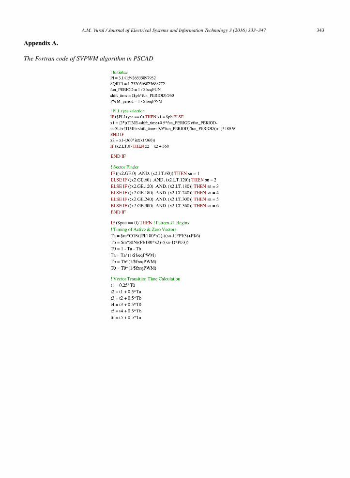
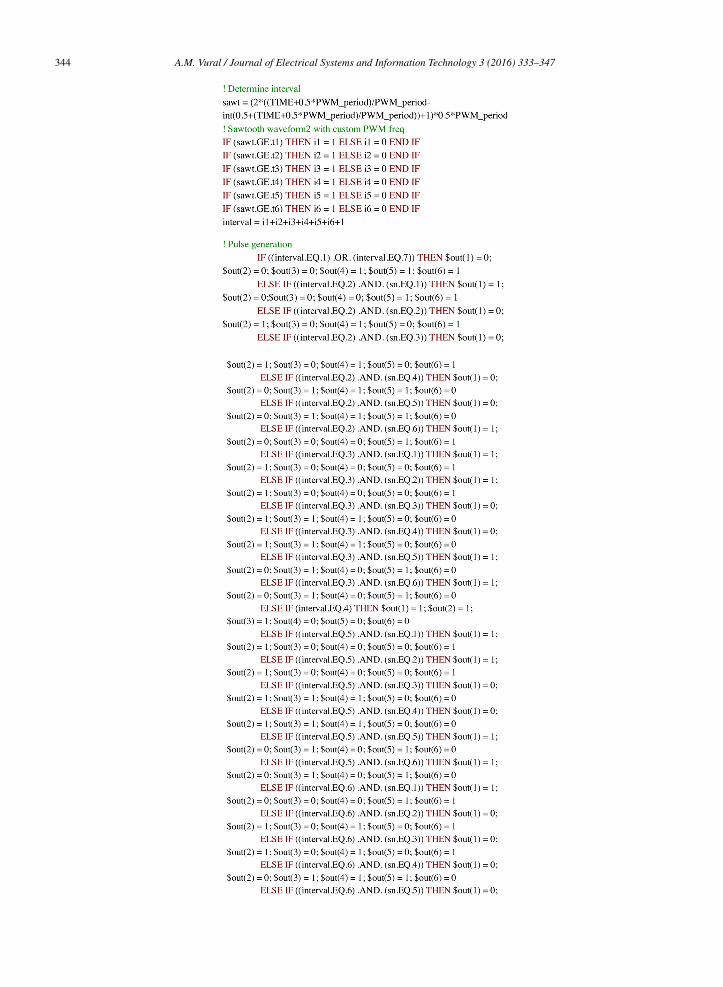
ppendix A.
he Fortran code of SVPWM algorithm in PSCAD
344 A.M. Vural / Journal of Electrical Systems and Information Technology 3 (2016) 333–347

A.M. Vural / Journal of Electrical Systems and Information Technology 3 (2016) 333–347 345

346 A.M. Vural / Journal of Electrical Systems and Information Technology 3 (2016) 333–347
References
Asiminoaei, L., Rodriguez, P., 2008a. Reduction of switching losses in active power filters with a new generalized discontinuous-PWM strategy.IEEE Trans. Ind. Electron. 55 (January (1)), 467–471.
Asiminoaei, L., Rodriguez, P., 2008b. Application of disconti-nuous PWM modulation in active power filters. IEEE Trans. Power Electron. 23 (July(4)), 1692–1706.
Bose, B.K., 2002. Modern Power Electronics and AC Drives. Prentice Hall, PTR, Upper Saddle River, New Jersey.Chen, Guoqiang, Kang, Jianli, Zhao, Junwei, 2013. Numeric analysis and simulation of space vector pulse width modulation. Adv. Eng. Softw. 65
(November), 60–65.Colak, Ilhami, Kabalci, Ersan, Bayindir, Ramazan, 2011. Review of multilevel voltage source inverter topologies and control schemes. Energy
Convers. Manag. 52 (February (2)), 1114–1128.Costa, A., Vilaragut, M., Travieso-Torres, J.C., Duarte-Mermoud, M., Munoz, J., Yznaga, I., 2012. Matlab based simulation toolbox for the study
and design of induction motor FOC speed drives. Comput. Appl. Eng. Educ. 20 (June (2)), 295–312.Demirkutlu, E., Hava, A.M., 2009. A scalar resonant-filter-bank-based output-voltage control method and a scalar minimum-switching-loss dis-
continuous PWM method for the four-leg-inverter-based three-phase four-wire power supply. IEEE Trans. Ind. Appl. 45 (May/June (3)),982–991.
Durgasukumar, G., Pathak, M.K., 2012. Comparison of adaptive neuro-fuzzy-based space-vector modulation for two-level inverter. Int. J. Electr.Power Energy Syst. 38 (June (1)), 9–19.
Geethalakshmi, B., Dananjayan, P., 2008. Investigation of performance of UPFC without DC link capacitor. Electr. Power Syst. Res. 78 (April (4)),736–746.
Holmes, D.G., 1996. The significance of zero space vector placement for carrier-based PWM schemes. IEEE Trans. Ind. Appl. 32 (September/October(5)), 1122–1129.
Holmes, D.G., Lipo, T.A., 2003a. Pulse Width Modulation for Power Converters. IEEE Press/Wiley Interscience, Piscataway, NJ/New York, ch. 6,ch. 6.
Holmes, D.G., Lipo, T.A., 2003b. Pulse Width Modulation for Power Converters: Principles and Practice. Wiley–IEEE Press, Piscataway, NJ.Holtz, J., 1992. Pulsewidth modulation—a survey. IEEE Trans. Ind Electron. 39 (October (5)), 410–420.Huang, Shoudao, Pham, D.C., Huang, Keyuan, Cheng, Shuangyin, 2012. Space vector PWM techniques for current and voltage source converters:
a short review. In: 15th International Conference on Electrical Machines and Systems (ICEMS), 2012, 21–24 October, pp. 1–6.Karimi-Davijani, H., Sheikholeslami, A., Ahmadi, R., Livani, H., 2008. Active and reactive power control of DFIG using SVPWM converter. In:
Universities Power Engineering Conference, 2008. UPEC 2008. 43rd International, 1–4 September, pp. 1–5.Liu, Jiajun, Yao, Lixiao, Wu, Tiansen, An, Yuan, 2010. Implementation of two-level SVPWM algorithm in PSCAD/EMTDC. In: 2010 Asia–Pacific
Power and Energy Engineering Conference (APPEEC), 28–31 March, pp. 1–5.Lu, H., Qu, W., 2007. A novel PWM technique with two-phase modulation. IEEE Trans. Power Electron. 22 (November (6)), 2403–2409.Monitoba Hydro International Ltd. https://hvdc.ca/pscad/versions.Muyeen, S.M., Mannan, M.A., Ali, M.H., Takahashi, R., Murata, T., Tamura, J., 2007. Simulation technique & application of space-vector PWM
method in PSCAD/EMTDC. In: International Conference on Information and Communication Technology, 2007. ICICT ‘07, 7–9 March, pp.1–4.
Norouzizadeh, R., Dastfan, A., Rafiei, S.M.R., Amirahmadi, A., 2010. Design and simulation of unified power flow controllers using matrixconverters. In: 2010 IEEE International Symposium on Industrial Electronics (ISIE), 4–7 July, pp. 773–778.
Omar, R., Rahim, N.A., 2009. Implementation and control of a dynamic voltage restorer using space vector pulse width modulation (SVPWM) forvoltage sag mitigation. In: 2009 International Conference for Technical Postgraduates (TECHPOS), 14–15 December, pp. 1–6.
Rashid, Muhammad H., 2013. Power Electronics: Circuits, Devices and Applications. Prentice Hall.Stumpf, Péter, Járdán, Rafael K., Nagy, István, 2013. Analysis of the impact of space vector modulation techniques on the operation of ultrahigh
speed induction machines. Math. Comput. Simul. 90, 132–144.Ün, E., Hava, A.M., 2009. A near-state PWM method with reduced switching losses and reduced common-mode voltage for three-phase voltage
source inverters. IEEE Trans. Ind. Appl. 45 (March/April (2)), 782–793.
Vafakhah, B., Salmon, J., 2010. Interleaved discontinuous space-vector PWM for a multilevel PWM VSI using a three-phase split-wound coupledinductor. IEEE Trans. Ind. Appl. 46 (April (5)), 2015–2024.Valan Rajkumar, M., Manoharan, P.S., 2013. FPGA based multilevel cascaded inverters with SVPWM algorithm for photovoltaic system. Sol.
Energy 87, 229–245.

V
W
WX
X
X
Y
A.M. Vural / Journal of Electrical Systems and Information Technology 3 (2016) 333–347 347
alan Rajkumar, M., Manoharan, P.S., Ravi, A., 2013. Simulation and an experimental investigation of SVPWM technique on a multilevel voltagesource inverter for photovoltaic systems. Int. J. Electr. Power Energy Syst. 52, 116–131.
ang, Bingsen, Cathey, Jimmie J., 2003. DSP-controlled, space-vector PWM, current source converter for STATCOM application. Electric PowerSyst. Res. 67 (November (2)), 123–131.
ikipedia, The Free Encyclopedia 2016. http://en.wikipedia.org/wiki/Sawtooth wave.iang, Liang, Wang, Yong, Zi, Zhenning, Huang, Jie, 2011. Research on space vector modulation control strategy based on 60◦ coordinate for
three-level active power filter. In: 2011 International Conference on Electrical Machines and Systems (ICEMS), 20–23 August, pp. 1–4.iao, Shiwu, Wang, Yuxi, Liu, Jianhui, 2011. SVPWM realization and application on passive network. In: Power and Energy Engineering Conference
(APPEEC), 2011 Asia–Pacific, 25–28 March, pp. 1–3.
iaojie, Zhou, Yi, Ruan, 2011. Modeling and simulation analysis of 3-level VSC-STATCOM based on SVPWM. 8–9 September In: PowerEngineering and Automation Conference (PEAM), 2011 IEEE, vol. 2, pp. 111–114.u, Zhenyu, 2016. Space-Vector PWM With TMS320C24x/F24x Using Hardware and Software Determined Switching Patterns, Application Report
SPRA524. Texas Instruments.