PROPERTIES OF GRAPHENE NANORIBBONS OBTAINED BY …PROPERTIES OF GRAPHENE NANORIBBONS OBTAINED BY...
38
PROPERTIES OF GRAPHENE NANORIBBONS OBTAINED BY CHEMICAL VAPOR DEPOSITION BY AUSTIN S. LYONS THESIS Submitted in partial fulfillment of the requirements for the degree of Master of Science in Electrical and Computer Engineering in the Graduate College of the University of Illinois at Urbana-Champaign, 2011 Urbana, Illinois Adviser: Assistant Professor Eric Pop
Transcript of PROPERTIES OF GRAPHENE NANORIBBONS OBTAINED BY …PROPERTIES OF GRAPHENE NANORIBBONS OBTAINED BY...

PROPERTIES OF GRAPHENE NANORIBBONS
OBTAINED BY CHEMICAL VAPOR DEPOSITION
BY
AUSTIN S. LYONS
THESIS
Submitted in partial fulfillment of the requirements
for the degree of Master of Science in Electrical and Computer Engineering
in the Graduate College of the
University of Illinois at Urbana-Champaign, 2011
Urbana, Illinois
Adviser:
Assistant Professor Eric Pop

ii
ABSTRACT
We use chemical vapor deposition (CVD) to synthesize graphene films on copper foil.
After transferring the graphene to SiO2/Si substrates, we pattern the film into graphene nanorib-
bons (GNRs) of width < ~50 nm and length < ~ 700 nm with Ti/Au contacts. We perform low-
bias, high-bias, and temperature-dependent electrical measurements. CVD-grown GNRs have
mobility values from 100 to 500 cm2V
-1s
-1 and current densities up to ~3 mA/µm, suggesting that
polycrystalline graphene grain boundaries play a limited role in the CVD-GNR electrical proper-
ties. CVD-GNR Raman spectra are comparable to lithographically patterned GNRs from exfoli-
ated graphene. We fit our experimental data using a self-consistent model that includes GNR
fringing capacitance and observe a weak temperature dependence of CVD-GNR mobility. We
find a square root dependence of maximum current density on GNR resistance, implying that
breakdown is primarily due to Joule heating. The electrical characteristics of CVD-GNRs illus-
trate the promise of wafer-scale graphene integration while revealing variability, contacts, and
impurities as future challenges for improving performance.

iii
To my wife Emily for her love and support

iv
ACKNOWLEDGMENTS
I would like to thank my adviser Eric Pop for the opportunity to join his research team at
the University of Illinois at Urbana-Champaign. I am grateful for his support and guidance. I
thank my Pop Lab colleagues for welcoming me into their group and spending countless hours
sharing their knowledge with me; they are a remarkable group of people. A special thanks to
Myung-Ho Bae, Ashkan Behnam, Vince Dorgan, David Estrada, Albert Liao, and Josh Wood for
the experimental training and assistance they provided. Thanks to Sharnali Islam for her simula-
tion and modeling help. For their technical support, I thank the staff of the Micro and Nanotech-
nology Laboratory (MNTL) clean room. In particular, Edmond Chow helped with the electron-
beam lithography in this work. I am very appreciative of the seminars hosted in MNTL because
they regularly provided two of my favorite things: intellectual stimulation and free pizza. Final-
ly, I thank my wife, family, and friends for all of their love and support. This work was support-
ed in part by the Air Force Office of Scientific Research (AFOSR).
v
TABLE OF CONTENTS
CHAPTER 1 INTRODUCTION ................................................................................................... 1
1.1 Introduction to Graphene .............................................................................................. 1
1.2 Graphene Nanoribbon Field-Effect Transistors ............................................................ 3
1.3 Graphene Nanoribbon Interconnects ............................................................................ 4
1.4 Chemical Vapor Deposition of Graphene ..................................................................... 4
1.5 Figures........................................................................................................................... 7
CHAPTER 2 EXPERIMENTAL PROCEDURES ...................................................................... 12
2.1 Graphene Growth and Transfer .................................................................................. 12
2.2 GNR Fabrication ......................................................................................................... 13
2.3 Raman Characterization of CVD GNRs ..................................................................... 14
2.4 Figures......................................................................................................................... 15
CHAPTER 3 ELECTRICAL CHARACTERIZATION OF CVD GRAPHENE
NANORIBBONS .......................................................................................................................... 18
3.1 Low-Bias Measurements ............................................................................................ 18
3.2 Temperature-Dependent Measurements ..................................................................... 20
3.3 High-Bias Measurements ............................................................................................ 20
3.4 Figures......................................................................................................................... 23
CHAPTER 4 CONCLUSION...................................................................................................... 29
APPENDIX DERIVATION OF EQUATION (3.3) .................................................................... 30
REFERENCES ............................................................................................................................. 32

1
CHAPTER 1
INTRODUCTION
1.1 Introduction to Graphene
Silicon transistors have been the fundamental building blocks of the semiconductor industry
for several decades. Improvements in fabrication techniques and technologies allowed device
designers to iteratively shrink silicon transistor dimensions, resulting in faster and cheaper elec-
tronics. In turn, these powerful and cheap transistors spawned a spectrum of silicon-based elec-
tronics, enabling technical, economic, and social improvements. However, silicon transistor scal-
ing trends are approaching the physical limits of silicon.1 With the future of the semiconductor
industry in limbo, forward-thinking researchers in industry and academia have been searching
for new materials with better electronic properties to supplement or replace silicon. Graphene is
one such material.
Graphene, a two-dimensional sheet of hexagonally arranged carbon atoms, was first isolated
and electrically measured in 2004 by scientists at the University of Manchester.2 Realizing that
graphite is simply stacked layers of graphene, the scientists (now Nobel laureates) devised a
method dubbed “mechanical exfoliation” to obtain single layer graphene. In general, mechanical
exfoliation uses a type of adhesive tape (e.g. ScotchTM
tape) to peel away layers of graphite with
the hope that enough peeling will thin some of the graphite down to only a few layers. The
graphite flakes are then transferred to a substrate; in our lab we simply press the Scotch tape
against a substrate and then slowly peel it off, leaving some of the graphite behind. After trans-
ferring the graphite to a substrate, one must undertake the monumental task of finding single lay-
er graphene (Fig. 1.1(a)) (placed at end of chapter) in the midst of a graphite mess (Fig. 1.1(b)).
Monolayer graphene is only one atom thick, yet it produces a slight change in optical contrast if

2
the underlying substrate is a particular thickness.3 Therefore, with the right substrate, a good mi-
croscope, and patience, one can find single layers graphene up to ~50 μm in size.
After graphene was successfully isolated, its electrical properties were explored.2,4-6
Experi-
ments revealed an ambipolar electric field effect in graphene (Fig 1.2(a)), which means that con-
duction can occur via electrons, holes, or a combination of both (Fig 1.2(b)). Charge carrier con-
centrations as high as 1013
cm-2
with mobility values μ > 15,000 cm2 V
-1 s
-1 were reported. Be-
cause mobility is a measure of how quickly charge carriers can move through a material, the high
mobility of graphene is desirable for high-frequency applications. High-speed graphene transis-
tors were fabricated and intrinsic cutoff frequencies over 100 GHz were demonstrated.7 In addi-
tion to desirable electronic properties, the atomically thin planar structure of graphene is suitable
for modern integrated circuit manufacturing processes. A thin MOSFET channel suppresses
short-channel effects in semiconducting transistors.8 Graphene promises manufacturable transis-
tor technology that can be scaled to the ultimate thickness limit8 (single atom) while operating at
very high frequencies7,9,10
and large current densities.
Though it has many desirable properties for electronic applications, graphene also has some
important shortcomings. First and foremost, graphene lacks an energy band gap, which is neces-
sary for the operation of low-power, high-fidelity digital circuits with large ION/IOFF ratios > 104
at (and above) room temperature. Without a band gap, the on/off ratio of graphene is only modu-
lated by the density of states and is typically only 10 ~ 100. In digital applications with billions
of transistors, leaky graphene devices would consume a prohibitive amount of power. Secondly,
fabricated devices behave differently than ideal graphene; many devices have asymmetric con-
duction, varying minimum conductivity (Dirac) voltages V0, and hysteretic curves (Fig 1.3).
Therefore, an open research problem is to fabricate graphene transistors with repeatable charac-

3
teristics, a Dirac voltage V0 = 0 Volts, and a high ION/IOFF ratio. Regardless of its shortcomings,
the discovery of such a promising electronic material has had an enormous impact on the direc-
tion of semiconductor research.4
1.2 Graphene Nanoribbon Field-Effect Transistors
Initial graphene experiments were on micrometer-sized graphene. However, state-of-the-art
silicon field-effect transistors (FETs) for digital applications have minimum feature sizes on the
order of tens of nanometers.1 Therefore, a reasonable question is whether nanometer graphene
will have the same excellent electrical properties as micrometer graphene. To answer this, re-
searchers began studying the properties of graphene strips with widths less than 100 nm. Such
small structures are called graphene nanoribbons (GNRs). Early theoretical studies determined
that GNRs with zizag edges (Fig. 1.4(a)) behave as metallic conductors, while GNRs with arm-
chair edges (Fig 1.4(b)) are semiconductors.11
Another theoretical study revealed an inverse rela-
tionship between armchair GNR width and band gap magnitude.12
In 2007, a team from Colum-
bia University experimentally confirmed this inverse relationship by lithographically patterning
GNRs and measuring their conductance at low temperatures (Fig 1.5).13
We note that such exper-
imental GNR edges have a combination of zigzag and armchair segments, most likely terminated
by H or O atoms.14
Further experimental studies used alternative methods15-17
to create narrow
(<10 nm) GNRs with finite transport or energy band gaps and room temperature ION/IOFF ratios
up to 107.
While these experiments demonstrate that it is possible to engineer a band gap for GNRs,
several challenges still remain. The Columbia study used mechanical exfoliation to obtain gra-
phene, which is not a scalable fabrication technique. Alternative fabrication methods suffer from

4
low yield, result in a random distribution of GNR sizes, and are unable to precisely position the
GNRs.15-17
All GNRs suffer from edge scattering and therefore have mobility values much lower
than micron-scale graphene,18
sometimes even lower than silicon. Because experimental data
reveal gaps much larger than theoretical predictions, it has been suggested that the observed
transport gap is actually dominated by localized states from edge roughness and disorder.19
Fu-
ture work is needed to understand the cause of the transport gap. Nevertheless, it is clear that en-
ergy gaps appear in graphene nanoribbons and provide the band gap necessary for GNRs to be a
viable material for digital FETs.
1.3 Graphene Nanoribbon Interconnects
As silicon FET dimensions are shrinking, so are the conductive wires used to connect FET
terminals.20
These interconnects need to have low resistivity, high current capability, resistance
to electromigration, high mobility, and the ability to be defined using conventional fabrication
methods.21
Mechanically exfoliated GNRs have been shown to have resistivity comparable to
copper interconnects,22
breakdown current density >108 A/cm
2,22
immunity to electromigra-
tion,23
and can be defined using standard lithography and etching techniques.22
In addition, with
a thermal conductivity comparable to or higher than that of copper,24
GNR interconnects could
double as heat dissipaters to combat the growing interconnect Joule heating problem.20
These
desirable properties have generated interest in using GNRs as interconnects in hybrid graphene-
Si circuits25
and all graphene circuits.26
1.4 Chemical Vapor Deposition of Graphene
While mechanical exfoliation is a suitable method for obtaining high-quality flakes of gra-
phene for laboratory experiments, it is not capable of scaling for wafer-scale applications. In-

5
stead, large-area graphene films are needed. Graphene films were first synthesized by epitaxy,27
which produces graphene on an insulating SiC substrate. However, this method requires ex-
tremely high temperatures (over 1500 ºC), ultra-low pressures, and expensive ultra-high vacuum
equipment. A cheaper, lower temperature, higher pressure method of growing predominantly
monolayer graphene uses chemical vapor deposition (CVD) of carbon-containing gases on a me-
tallic substrate. A promising method of growing graphene on copper (Cu) foil was developed in
2009 by a group at the University of Texas at Austin.28
CVD synthesis of graphene on Cu begins by loading a 25 μm thick Cu foil into a hot wall
CVD furnace. Next, the foil is heated to 1000 ºC under a 2 sccm H2 flow at a pressure of 40
mTorr. When the system reaches 1000 ºC, 35 sccm of CH4 is introduced to begin the graphene
growth. During this key step of the process, methane molecules crack on the hot Cu surface.
Carbon atoms from the methane chemically adsorb to the Cu at nucleation sites while the hydro-
gen atoms from the methane float away. As the carbon atoms cluster to the nucleation sites, indi-
vidual graphene domains are created (Fig. 1.6). The growth rate of each graphene domain is a
function of the underlying Cu substrate crystallography.29
This surface catalyzed growth is self-
limited, resulting in graphene films with over 90% monolayer coverage28
(the rest is multilayer).
The synthesized graphene grows on both sides of the copper, and the dimensions are only limited
by the size of foil.
CVD graphene has its share of imperfections. It contains resistive grain boundaries (GBs) at
the intersection of graphene domains.30
The difference in thermal expansion between Cu and
graphene creates wrinkles in the graphene film. Finally, the CVD graphene must be removed
from the copper foil and transferred to a more suitable substrate for electronic applications,
which requires significant handling and chemical processing. These problems are known to de-
6
crease the mobility of micron-scale graphene. Regardless, large-area CVD graphene has already
been used by Samsung to create graphene-based touch panels and 30 inch graphene films (Fig.
1.7).31
Graphene films synthesized by chemical vapor deposition are very useful for future wafer-
scale nanoelectronics that use GNRs as interconnects or transistors. It is well known that micron-
scale exfoliated graphene has better electrical properties than CVD graphene. However, very lit-
tle CVD GNR data exists today. GNRs made from CVD-grown graphene could be comparable
to or smaller than the average graphene grain size, and therefore have few or no grain bounda-
ries, few or no wrinkles, and fewer impurities than large-area CVD graphene. In this case, the
electrical characteristics of CVD GNRs and exfoliated GNRs may be quite similar, enabling
large-scale integration of high-quality CVD GNR transistors or interconnects.
In this thesis we present a comprehensive analysis of CVD GNRs. We perform low-bias,
high-bias, and temperature-dependent measurements on GNRs with various dimensions. The
mobility, current density, and Raman spectra of CVD-grown GNRs are comparable to exfoliated
and chemically derived GNRs, suggesting that polycrystalline grain boundaries play a limited
role in the CVD GNR electrical properties. We fit the data using a self-consistent model that in-
cludes GNR fringing capacitance. Our model reveals a weak temperature dependence of CVD
GNR mobility. Square root power dependence of maximum current density on the resistance of
the GNRs implies that breakdown is mainly due to Joule heating. The electrical characteristics of
CVD GNRs illustrate the promise of wafer scale graphene integration while revealing variability,
contacts, and impurities as future challenges for improving performance.

7
1.5 Figures
Figure 1.1(a) A large piece of single-layer exfoliated graphene on a 90 nm SiO2/Si++ sub-
strate. The bottom left corner is thick graphite. The slight difference in optical contrast of the
atomically thin graphene makes it very difficult to find graphene flakes. This picture is taken
with a 50x microscope lens. (b) A 5x image of exfoliated graphite. The arrow points to the
graphite which the graphene is located near.
(a)
(b)

8
Figure 1.2(a) The ambipolar electric field effect in graphene.4 A positive (negative) gate
voltage VG induces electrons (holes) in the graphene. (b) A MATLAB analysis of charge carrier
density in graphene as a function of gate voltage for a graphene FET on 90 nm SiO2 at room
temperature. Holes are the majority carriers for VG-V0 < 0, electrons are majority carriers for VG-
V0 > 0, and near V0 holes and electrons are similar in density.
-4 -2 0 2 410
9
1010
1011
1012
VG (V)
n,p
(cm
-2)
(a)
(b)
holes electrons
total

9
Figure 1.3 R-VG curve in air at room temperature for an exfoliated monolayer graphene FET
on SiO2/Si with width W = 14 μm, length L = 21 μm on 90 nm SiO2. The drain voltage VDS = 20
mV. VG was swept from 0 to +20, down to -20, and back to 0 in 200 mV increments. The Dirac
voltage of this device is V0 13~16 V, with the uncertainty due to hysteresis. ION/IOFF of this de-
vice is ~5 and hole mobility is μp ~ 1500 cm2V
-1s
-1. Inset, borrowed from Liao,
32 is a schematic
of the graphene FET.
Figure 1.4 (a) Semiconducting GNRs have a band gap that depends on ribbon width and
length,12,33
while (b) zigzag GNRs are metallic.34
(b) (a)

10
Figure 1.5 Experimental results from a Columbia University study demonstrating the inverse
relationship between band gap and GNR width.13
We observe that GNRs with widths W > 25 nm
have band gaps smaller than the room temperature thermal excitation energy (kBT/q, ~26 millie-
lectron volt, where kB is the Boltzmann constant and T is the absolute temperature).
Figure 1.6 Scanning electron microscope (SEM) image of graphene on Cu foil after a one
minute partial growth.28
The graphene domains begin at a nucleation site and fan outward as time
progresses. The intersections of graphene domains are called grain boundaries.

11
Figure 1.7 Researchers from Samsung have demonstrated (a) a graphene-based touch screen
and (b) a 30 inch graphene film.31
(a) (b)

12
CHAPTER 2
EXPERIMENTAL PROCEDURES
2.1 Graphene Growth and Transfer
Our CVD graphene growth and GNR device process steps are illustrated in Fig. 2.1. We
begin by loading 1 mil copper foil (~99.9% purity, Basic Copper, Carbondale, IL) into an Ato-
mate CVD system. The foil is cut into a rectangle and wrapped around a quartz boat. We load the
boat with Cu foil into a quartz tube. This tube is dedicated to growing graphene in an effort pre-
vent cross contamination with other CVD processes. The Cu foil is kept as smooth as possible
during these steps to minimize wrinkles and tears in the synthesized graphene. The temperature
is ramped to 1000 °C under H2/Ar flow and the Cu foil is kept at 1000 °C under H2/Ar flow for
one hour to increase Cu foil grain size.28
Graphene growth is performed by flowing 100 sccm
CH4 at 1000° C and 500 mTorr chamber pressure for 30 minutes, which results primarily in
monolayer graphene growth on both sides of the Cu foil28
(Fig. 2.1(a)). The system was cooled at
a rate of ~20 °C under H2/Ar flow.
We remove the foil from the quartz tube and prepare the graphene for transfer from the foil
to an SiO2/Si++ substrate. The foil with graphene on it is gently cut into squares roughly the size
of the substrates used (22 mm x 22 mm). One side of the foil is covered with ~250 nm thick lay-
er of polymethyl methacrylate (PMMA) to protect the graphene, while the other side is left ex-
posed. We remove the graphene from the exposed side of the Cu foil with a 20 sccm O2 plasma
reactive ion etch (RIE) for 10 seconds (Fig. 2.1(b)). It is worth noting that we use the graphene
from the side of the foil that was in contact with the quartz boat because it tended to have better
Raman spectra (smaller D peak) than graphene from the opposite side of the foil. After RIE, the
remaining Cu foil/graphene/PMMA stack is placed in a beaker of aqueous FeCl3 overnight to

13
etch away the Cu (Fig. 2.1(c)). After the foil is completely etched, we are left with the gra-
phene/PMMA film floating on the surface of the FeCl3. The PMMA/graphene film is transferred
via a glass slide to an HCl bath to functionalize Cu particle contamination35
and then to two sep-
arate deionized water baths to wash away the HCl (Fig. 2.1(d)). After the film is clean, it is trans-
ferred to an SiO2 (90 nm ± 5 nm) on Si (N doped 5 mΩ⋅cm) substrate and left overnight to dry
(Fig. 2.1(e)). The PMMA is removed by submerging the substrate in a 1:1 mixture of methylene
chloride and methanol for one hour. Finally, the graphene is annealed with a one hour Ar/H2 an-
neal at 400 °C at atmospheric pressure to remove the PMMA and other organic residue36
(Fig.
2.1(f)). This step does not completely remove the PMMA residue (Fig 2.2), preventing metal
electrodes from completely contacting the graphene and leading to a higher contact resistance.
Improving GNR contacts is a very important challenge that must still be addressed to increase
GNR performance while reducing variability.
2.2 GNR Fabrication
GNR devices are fabricated by defining large Ti/Au (0.5/40 nm) probing contacts using opti-
cal lithography and electron-beam (e-beam) evaporation (Fig 2.2). An additional step of e-beam
lithography and evaporation is performed to create smaller finger contacts defining the length of
the devices in the nanometer regime (Fig. 2.3(a)). We use a bilayer resist (495 PMMA A2 & 950
PMMA A4 from MicroChem) to help with metal liftoff for all e-beam lithography steps. The
width of the GNR is defined with a second e-beam lithography step, and after the PMMA is de-
veloped, 1 to 2 nm of Al is deposited using e-beam evaporation. The thin evaporated Al film ox-
idizes when the chip is removed from the low-pressure e-beam evaporation chamber.37
PMMA
liftoff leaves behind an AlOx nanoribbon covering the graphene and stretching between finger
electrodes (Fig. 2.3(a)). Because liftoff of a 1-2 nm evaporated Al film can be surprisingly diffi-
14
cult (Fig. 2.4), one may opt to evaporate a thicker (e.g. 20 nm) metal mask for etching the CVD
graphene into ribbons.38
A 10 second O2 plasma RIE at 40 Watts and 40 mTorr removes all un-
protected graphene and leaves a GNR under the etch mask (Fig. 2.1(g)). The etch parameters can
be tuned during this step to laterally etch the protected GNR at the edges, thus achieving GNR
widths smaller than the minimum resolution afforded by e-beam lithography.38
The CVD gra-
phene under the contacts is also protected during the plasma etch, achieving a larger graphene-
metal contact area and reduced contact resistance. Because the AlOx etch mask can double as a
seed layer for future top gate deposition,37
we left the AlOx etch mask on some devices (batch
b1) for the measurements. For comparison, we also removed the AlOx etch mask (Figure 2.3(b))
using Al etch type A (Transene Company Inc.) on a subset of the devices (batch b2) to compare
the AlOx covered CVD GNRs with bare CVD GNRs.
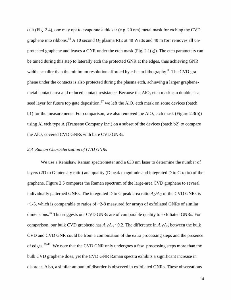
2.3 Raman Characterization of CVD GNRs
We use a Renishaw Raman spectrometer and a 633 nm laser to determine the number of
layers (2D to G intensity ratio) and quality (D peak magnitude and integrated D to G ratio) of the
graphene. Figure 2.5 compares the Raman spectrum of the large-area CVD graphene to several
individually patterned GNRs. The integrated D to G peak area ratio AD/AG of the CVD GNRs is
~1-5, which is comparable to ratios of ~2-8 measured for arrays of exfoliated GNRs of similar
dimensions.39
This suggests our CVD GNRs are of comparable quality to exfoliated GNRs. For
comparison, our bulk CVD graphene has AD/AG ~0.2. The difference in AD/AG between the bulk
CVD and CVD GNR could be from a combination of the extra processing steps and the presence
of edges.39,40
We note that the CVD GNR only undergoes a few processing steps more than the
bulk CVD graphene does, yet the CVD GNR Raman spectra exhibits a significant increase in
disorder. Also, a similar amount of disorder is observed in exfoliated GNRs. These observations

15
suggest that disorder in GNR Raman spectra is more likely due to GNR edges than the extra pro-
cessing steps of CVD graphene.
2.4 Figures
Figure 2.1 Schematic of the CVD growth on Cu and transfer process to SiO2 (90 nm)/Si sub-
strates (a-e) and fabrication of devices (f-h). The substrate is used as the back gate in electrical
measurements. A thin AlOx layer is used as an etch mask to form GNRs (h), which is later re-
moved for some of the devices (batch b1).
Figure 2.2 Optical micrograph of a row of devices on a test chip. Micron-scale PMMA residues
(light blue) are sometimes visible even after annealing. Dark purple areas are bilayer graphene.
Scale bar is 300 μm.
Source electrode Drain electrode
Finger electrodes
PMMA residue Bilayer graphene

16
Figure 2.3 (a) An SEM image of a W = 75 nm L = 110 nm GNR between two Ti/Au (1/40 nm)
finger contacts (scale bar = 1 μm). The AlOx ribbon can be seen over the contacts. (b) AFM of a
W = 60 nm L = 400 nm CVD GNR. Scale bar is 100 nm.
Figure 2.4 Optical micrograph of an unsuccessful AlOx liftoff. The optical contrast is from the
~2 nm AlOx film. Scale bar is 300 μm.
(a) (b)
AlOx covered region
Source electrode
No AlOx
Source electrode
Edge of AlOx film
contact

17
Figure 2.5 Raman spectra for bulk CVD graphene and GNR devices, indicating good quality
and predominantly monolayer coverage for the bulk CVD graphene and the presence of defects
and edge states for the GNR. Some GNRs have visible D′ peaks, another indication of defects.
D G 2D
D
W/L = 30/100 nm
W/L = 30/500 nm
W/L = 40/600 nm
W/L = 40/600 nm
W/L = 50/500 nm

18
CHAPTER 3
ELECTRICAL CHARACTERIZATION OF CVD GRAPHENE NANORIBBONS
3.1 Low-Bias Measurements
We apply a low-field drain bias VD and measure the drain current ID of the CVD GNRFET
as a function of the back gate voltage VG. All sourced voltages and measured currents are manip-
ulated and recorded via a Keithley 4200 Semiconductor Characterization System. VG is applied
to the heavily doped Si++ back gate on the bottom of the substrate which behaves like a metal
electrode. Modulation of VG shifts the Fermi level of the GNR, modulating the density of charge
carriers. Measuring ID as a function of VG allows us to view the modulation of charge density and
quantitatively characterize the electrical behavior of our CVD GNRs.
Measurements of both AlOx capped and bare CVD GNRs in vacuum (~10-5
Torr) at room
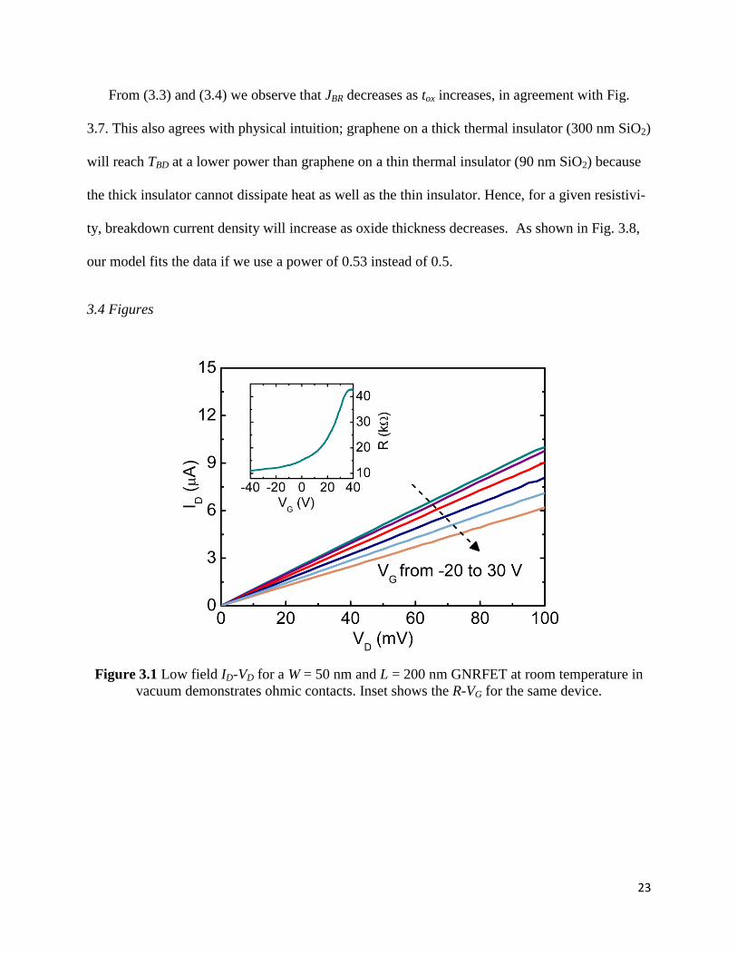
temperature reveal p-doped GNRs with ohmic contacts and varying ION/IOFF. Some devices have
visible minimum conductivity voltages V0, while other devices have a V0 beyond our maximum
“safe” back gate voltage (~40 V) (Fig. 3.1). Annealing the GNRs at 300 ºC for two hours in vac-
uum removes the physisorbed ambient impurities such as water2 and oxygen.
41 After annealing,
measurements in vacuum show the devices are less p-doped than in air and in some cases n-
doped (Fig. 3.2). The data are fitted with a transport model42
(Fig. 3.3) revealing channel mobili-
ty μ = 100~500 cm2V
-1s
-1 and contact resistance RCW ≥ 500 Ω⋅μm. The model includes thermal-
ly generated carriers, contact resistance as a function of gate voltage and temperature, puddle
charge density, and the effect of fringing fields on the capacitance between the back-gate and
GNR through the SiO2 substrate32,43
(Fig. 3.4). Our equation for the classical capacitance per unit

19
area is modified to include the fringing field capacitance based on the approach introduced by
Liao32
oxox
oxoxtWWt
C1
16ln0
(3.1)
The first term in Equation 3.1 represents the GNR fringing capacitance and the second term is
the GNR parallel plate capacitance. In the limit W→ ∞, the equation reduces to the classical
ox
oxox
tC 0
(3.2)
as expected. In our case, quantum capacitance44
can be neglected due to the thickness of the bur-
ied oxide (~90 nm). Including the fringing capacitance of the GNR is important, as it leads to a
correct extraction of the mobility, which appears lower than if the fringing effect is not included.
Therefore, it is important that device and circuit engineers include GNR fringing capacitance in
their analysis and models.
The extracted mobility values of our CVD GNRs (up to ~500 cm2V
-1s
-1) are comparable
to lithographically patterned exfoliated GNRs45
(200~1000 cm2V
-1s
-1 ) and mostly lower than
chemically derived GNRs17,32, 46
(300~1500 cm2V
-1s
-1). The similarity of exfoliated and CVD
GNR mobilities is different than micron-scale CVD devices,28
which consistently show lower
mobility than exfoliated graphene. This suggests GBs play less of a role in lowering GNR mobil-
ity than edge roughness scattering introduced from lithography. We believe that this is a conse-
quence of the GNR dimensions being comparable to or smaller than the GB size of CVD-grown
graphene.

20
3.2 Temperature-Dependent Measurements
We perform low-field measurements on AlOx capped GNRs in a vacuum probe station as a
function of temperature. After pumping down to ~10-5
torr vacuum, we heat the chuck that the
substrate sits on to 300 ºC and let the GNR anneal for two hours. Next, we use liquid nitrogen to
cool the vacuum probe station to ~80 K. After measurements at 80 K , we turn the heater on to
increase the temperature of the probe station. When the temperature reaches ~120 K, we turn the
heater off and repeat our measurements. Data is obtained in ~40 K increments until ~360 K. We
fit the experimental results with our model and observe a weak dependence of mobility on tem-
perature for two W = 40 nm GNRs over a temperature range of 80 to 360 K (Fig. 3.5). The mo-
bility of a W = 20 nm GNR mobility increases up to room temperature and then slightly decreas-
es with above room temperature. An increase in mobility with temperature can be an indication
of charged impurity scattering limited low-field transport.18,42
Alternatively, recent works47,19
treat GNRs as electron and hole puddles approximately the size of their width. From this point of
view, the apparent increase in mobility could be due to temperature-activated puddle hopping
transport. Further systematic study is needed to determine the mechanism behind the temperature
dependence of mobility in CVD GNRs.
3.3 High-Bias Measurements
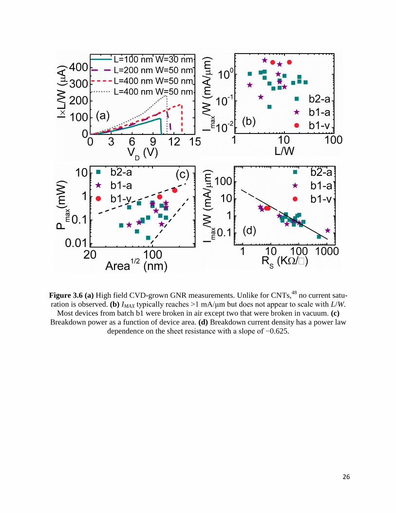
To investigate the maximum current capacity (Imax) of the CVD GNRs, we perform room
temperature, high-field ID-VD measurements in air for 22 GNRs with widths W = 15 to 50 nm
and lengths L = 100 to 700 nm. VD is incrementally increased until the GNR stops conducting
due to physical breakdown which occurs at ~600 ºC in air for graphene nanoribbons.32,48
We
measure the drain current ID as a function of drain voltage VD. Figure 3.6(a) shows representative

21
data obtained from four GNRs. Unlike in carbon nanotube FETs48
and large-area exfoliated gra-
phene FETs,49
current saturation is not observed in these GNRFETs before breakdown.
Maximum current densities in each batch are relatively high.50
The devices capped by an
AlOx layer (Fig. 3.6(b), batch b1) show average Imax ~ 0.7 mA/μm, with the highest Imax ~ 1.2
mA/μm. For other devices (without the protective AlOx layer, batch b2) we found peak current
density Imax ~ 1.3 mA/μm, with the highest value of ~3.4 mA/μm in air for the widest device
measured (W ~ 50 nm). Due to variation and small sample size, it is not clear if the GNRs with
an AlOx capping layer will always break at higher current densities than uncovered CVD GNRs.
Two AlOx capped GNRs measured in vacuum both exhibited Imax ~ 2.8 mA/μm.
As shown in Fig 3.6(b), no clear scaling between Imax and device dimensions (L/W ratio) is
found. Each batch of CVD GNRs has devices of similar L/W ratios that exhibit an order of mag-
nitude in Imax variation. This suggests that sample-to-sample variability from impurities,18,51
edg-
es,13,52,53
non-uniform graphene growth,29
and contacts54,55
remains a concern and must be further
improved.
The GNR breakdown power PBD scales approximately proportionally with GNR area (Fig.
3.6(c)), indicative of the role of heat dissipation from the GNR to the SiO2 under such high-bias
conditions.32,56
These GNRs also demonstrate a reciprocal relationship between breakdown cur-
rent density and nanoribbon resistivity as shown in Fig. 3.6(d), similar to exfoliated graphene
nanoribbons24
and CVD graphene microribbons.50
Using the relation Imax/W = Aρ-n
, the best fit
for the data yields n = 0.625 with R2 ≈ 0.75. Generally, a value of n close to unity suggests that
the breakdown is primarily due to the electric field, while a value close to 0.5 corresponds to
breakdown due to local heating at a certain temperature.50
Therefore, the value n ≈ 0.625 ob-

22
tained here suggests that breakdown is first initiated at locations that are heated. For narrow
GNRs, this probably results in the complete failure of the structure rather than being field-
dependent.
As shown in Fig. 3.7, the dependence of breakdown current density with resistivity is similar
to that of exfoliated GNRs and CVD graphene. However, for a given resistivity, the current car-
rying capacity of our CVD GNRs on 90nm SiO2 is higher than the capacity of exfoliated GNRs
and CVD graphene on 300 nm SiO2. To understand the relationship between breakdown current
density JBR, resistivity ρ, and oxide thickness tox, we use equations from Liao32
to obtain the fol-
lowing (see Appendix A for the full derivation)
5.0
12
sinh2
cosh
2sinh
2cosh
)( 0
H
TH
H
H
TH
H
g
BDBR
L
LRgL
L
L
L
LRgL
L
L
Wt
TTgJ
(3.3)
Here, TBD is the breakdown temperature, T0 is ambient temperature, tg is the thickness of gra-
phene, W is the width of the GNR, L is the length of the GNR, LH is the healing length along the
graphene, and RT is the thermal resistance at the metal contacts.
The heat loss coefficient into the substrate g is defined as
W
RW
t
k
Wt
kg Cox
ox
ox
ox
ox
1
1
)1/(6ln
, (3.4)
where RCox is the thermal boundary resistance at the graphene/oxide interface, kox is the thermal
conductivity of the oxide, and W is the width of the graphene nanoribbon.
23
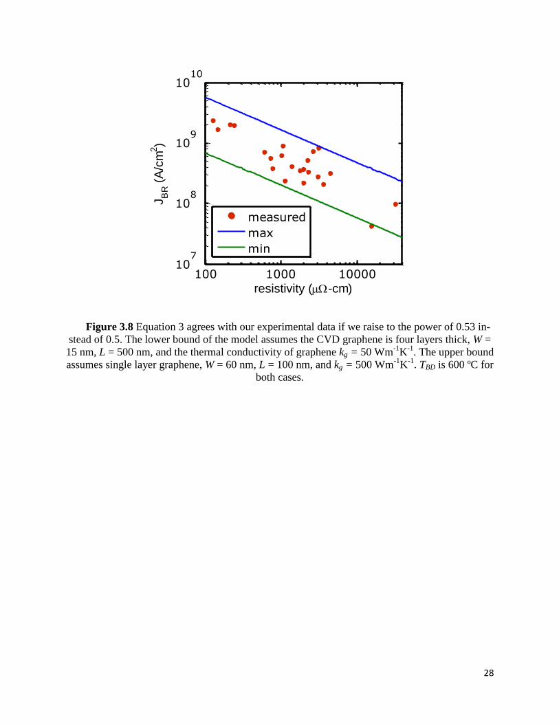
From (3.3) and (3.4) we observe that JBR decreases as tox increases, in agreement with Fig.
3.7. This also agrees with physical intuition; graphene on a thick thermal insulator (300 nm SiO2)
will reach TBD at a lower power than graphene on a thin thermal insulator (90 nm SiO2) because
the thick insulator cannot dissipate heat as well as the thin insulator. Hence, for a given resistivi-
ty, breakdown current density will increase as oxide thickness decreases. As shown in Fig. 3.8,
our model fits the data if we use a power of 0.53 instead of 0.5.
3.4 Figures
Figure 3.1 Low field ID-VD for a W = 50 nm and L = 200 nm GNRFET at room temperature in
vacuum demonstrates ohmic contacts. Inset shows the R-VG for the same device.

24
Figure 3.2 Annealing in vacuum at 300 ºC removes water and oxygen, shifting the Dirac point
closer to zero for a W = 40 nm, L = 400 nm CVD GNR.
Figure 3.3 An example of fitting experimental GNR data (circles) with our model (lines). To fit
the data for this W = 20 nm, L = 200 nm GNR, we use contact resistance RCON =700~1000 Ω⋅μm
and puddle charge density n0 = 1~4×10¹²
cm-2
.
-40 -20 0 20 400.5
1
1.5
2
2.5
3x 10
5
VG (V)
R (
)

25
Figure 3.4(a) A fringing field capacitance exists between the conductive GNR and the Si++
back gate.
Figure 3.5 Extracted hole mobility for three AlOx capped CVD GNRs. The GNRs exhibit a weak
dependence on temperature. The variation in mobility between the 20 nm and 40 nm CVD GNRs
is common; our CVD GNRs did not show a clear relationship between mobility and width. For
these GNRs, our model used puddle charge density n0 = 1~3×10¹²
cm-2
and contact resistance
RCON = 500~1000 Ω⋅μm to fit the experimental data.
26
Figure 3.6 (a) High field CVD-grown GNR measurements. Unlike for CNTs,48
no current satu-
ration is observed. (b) IMAX typically reaches >1 mA/μm but does not appear to scale with L/W.
Most devices from batch b1 were broken in air except two that were broken in vacuum. (c)
Breakdown power as a function of device area. (d) Breakdown current density has a power law
dependence on the sheet resistance with a slope of −0.625.

27
Figure 3.7 A similar dependence of breakdown current density on resistivity exists for large area
CVD graphene on 300 nm SiO2 (Lee et al.50
), CVD graphene nanoribbons on 90 nm SiO2 (our
work), and graphene nanoribbons patterned from exfoliated graphene on 300 nm SiO2 (Murali et
al.24
). Representative error bars are shown on four of the data points, and the CVD GNR data is
fit (black line) using the equation . Our devices on 90 nm oxide reach
higher JBR than the devices on 300 nm oxide due to better heat dissipation of the thinner oxide.
28
Figure 3.8 Equation 3 agrees with our experimental data if we raise to the power of 0.53 in-
stead of 0.5. The lower bound of the model assumes the CVD graphene is four layers thick, W =
15 nm, L = 500 nm, and the thermal conductivity of graphene kg = 50 Wm-1
K-1
. The upper bound
assumes single layer graphene, W = 60 nm, L = 100 nm, and kg = 500 Wm-1
K-1
. TBD is 600 ºC for
both cases.
100 1000 1000010
7
108
109
1010
resistivity (-cm)
JB
R (
A/c
m2)
measured
max
min

29
CHAPTER 4
CONCLUSION
We demonstrate large-scale fabrication of GNRs patterned from graphene grown by CVD.
Our CVD GNRs have higher current carrying capacities and similar mobilities compared to
GNRs fabricated using less scalable methods, suggesting that graphene grain boundaries play a
negligible role in CVD GNRs. CVD graphene has a small D peak in its Raman spectra, whereas
GNRs from both CVD and exfoliated graphene have sizeable disorder induced D and D′ peaks in
their Raman spectra. This supports the theory that CVD grain boundaries are negligible and
points to nanoribbon edges as a major concern affecting performance and variability. The excel-
lent current carrying capacity and the low ION/IOFF ratios suggest that lithographically patterned
CVD GNRs of dimensions W = 15–50 nm could be used in future large-scale integrated circuits
as interconnects, but are not yet adequate for field-effect transistors. Future work to narrow the
CVD ribbons and appropriately terminate edge dangling bonds is necessary to determine if a
band gap suitable for digital electronics will result from quantum confinement. Temperature-
dependent low-bias measurements reveal a weak temperature dependence of mobility. For a first
order approximation, circuit design engineers could model the mobility of CVD GNR intercon-
nects as temperature independent. In conclusion, CVD GNRs illustrate the promise of wafer-
scale graphene integration while revealing variability, contacts, and impurities as future chal-
lenges for improving performance.

30
APPENDIX
DERIVATION OF EQUATION (3.3)
To understand the relationship between breakdown current density JBR, resistivity ρ, and ox-
ide thickness tox, we begin with the heat equation along graphene devices from Liao32
.
12
sinh2
cosh
2sinh
2cosh
)( 0
H
TH
H
H
TH
H
BDBD
L
LRgL
L
L
L
LRgL
L
L
TTgLP (A.1)
Here, PBD is the breakdown power, TBD is the breakdown temperature, T0 is the ambient tem-
perature, L is the length of the graphene nanoribbon, LH is the thermal healing length along the
graphene, and RT is the thermal resistance at the metal contacts. The heat loss coefficient into the
substrate g is defined as
W
RW
t
k
Wt
kg Cox
ox
ox
ox
ox
1
1
)1/(6ln
, (A.2)
where RCox is the thermal boundary resistance at the graphene/oxide interface, kox is the thermal
conductivity of the oxide, and W is the width of the graphene nanoribbon.
To get PBD as a function of JBR and ρ, we first write PBD in terms of I and R. Combining the
definition of power IVPBD and Ohm’s law IRV we get
RIPBD
2 (A.3)

31
Next we define I in terms of JBR as gBRWtJI , where tg is the thickness of the graphene.
Defining R in terms of ρ gives gWt
LR
. Substituting these definitions into (A.3) gives PBD as a
function of JBR and ρ.
WLtJP gBRBD 2
(A.4)
Substituting (A.4) into (A.1) and rearranging yields JBR as a function of ρ and tox.
5.0
12
sinh2
cosh
2sinh
2cosh
)( 0
H
TH
H
H
TH
H
g
BDBR
L
LRgL
L
L
L
LRgL
L
L
Wt
TTgJ
(A.5)

32
REFERENCES
1 M. Ieong, B. Doris, J. Kedzierski, K. Rim, and M. Yang, Science 306, 2057 (2004).
2 K. S. Novoselov et al., Science 306, 666 (2004).
3 P. Blake et al., Applied Physics Letters 91, 063124 (2007).
4 A. K. Geim and K. S. Novoselov, Nature Materials 6, 183 (2007).
5 K. S. Novoselov et al., Nature 438, 197 (2005).
6 K. S. Novoselov et al., Proceedings of the National Academy of Sciences 30, 102 (2005).
7 L. Liao et al., Nature 467, 305 (2010).
8 F. Schwierz, Nature Nanotechnology 5, 487 (2010).
9 Y. M. Lin et al., Science 327, 662 (2010).
10 J. A. Robinson, M. Hollander, M. LaBella, K. Trumbull, R. Cavalero, and D. W. Snyder, Nano
Letters 11, 3875 (2011).
11 K. Nakada, M. Fujita, G. Dresselhaus, and M. Dresselhaus, Physical Review B 54, 17954 (1996).
12 V. Barone, O. Hod, and G. E. Scuseria, Nano Letters 6, 2748 (2006).
13 M. Y. Han, B. Özyilmaz, Y. Zhang, and P. Kim, Physical Review Letters 98, 206805 (2007).
14 K. A. Ritter and J. W. Lyding, Nature Materials 8, 235 (2009).
15 X. Li et al., Science 319, 1229 (2008).
16 X. Wang, Y. Ouyang, X. Li, S. Lee, H. Dai, Physical Review Letters 100, 206803 (2008).
17 L. Jiao, X. Wang, G. Diankov, H. Wang, and H. Dai, Nature Nanotechnology 6, 132 (2010).
18 T. Fang, A. Konar, H. Xing, and D. Jena, Physical Review B 78, 205403 (2008).
19 P. Gallagher, K. Todd, and D. Goldhaber-Gordon, Physical Review B 81, 115409 (2010).
20 J. Warnock, presented at the Design Automation Conference (DAC), 2011 48th
ACM/EDAC/IEEE, New York, NY 2011 (unpublished).
21 P. Kapur, J. P. McVittie, and K. C. Saraswat, Electron Devices, IEEE Transactions on 49, 590
(2002).
22 R. Murali, K. Brenner, Y. Yang, T. Beck, J. D. Meindl, Electron Device Letters, IEEE 30, 611
(2009).
23 T. Ragheb and Y. Massoud, presented at the Computer-Aided Design, 2008. ICCAD 2008.
IEEE/ACM International Conference on, 2008 (unpublished).
24 R. Murali, Y. Yang, K. Brenner, T. Beck, J. D. Meindl, Applied Physics Letters 94, 243114
(2009).
25 X. Chen et al., presented at the Electron Devices Meeting (IEDM), 2009 IEEE International,
2009 (unpublished).
26 Y. Tan, M. Qiang, S. Chilstedt, M. D. F. Wong, and D. Chen, presented at the Design
Automation Conference (ASP-DAC), 2011 16th Asia and South Pacific, 2011 (unpublished).
27 C. Berger et al., Science 312, 1191 (2006).
28 X. Li et al., Science 324, 1312 (2009).
29 J. D. Wood, S. W. Schmucker, A. S. Lyons, E. Pop, and J. W. Lyding, Nano Letters 11, 4547
(2011).
30 Q. Yu et al., Nature Materials 10, 443 (2011).
31 S. Bae et al., Nature Nanotechnology 5, 574 (2010).
32 A. Liao et al., Physical Review Letters 106, 256801 (2011).
33 F. J. Owens, The Journal of Chemical Physics 128, 194701 (2008).
34 N. Gorjizadeh and Y. R. Kawazoe, Journal of Nanomaterials 2010 (2010).
35 B. Aleman et al., ACS Nano 4, 4762 (2010).
36 M. Ishigami, J. H. Chen, W. G. Cullen, M. S. Fuhrer, and E. D. Williams, Nano Letters 7, 1643
(2007).
37 S. Kim et al., Applied Physics Letters 94, 062107 (2009).
38 C. Lian, K. Tahy, T. Fang, G. Li, H. G. Xing, and D. Jena, Applied Physics Letters 96, 103109
(2010).
33
39 S. Ryu, J. Maultzsch, M. Y. Han, P. Kim, and L. E. Bruis, ACS Nano 5, 4123 (2011).
40 D. Bischoff, J. Güttinger, S. Dröscher, T. Ihn, K. Ensslin, and C. Stampfer, Journal of Applied
Physics 109, 073710 (2011).
41 L. Liu et al., Nano Letters 8, 1965 (2008).
42 V. E. Dorgan, M.-H. Bae, and E. Pop, Applied Physics Letters 97, 082112 (2010).
43 A. A. Shylau, J. W. Klos, and I. V. Zozoluenko, Physical Review B 80, 205402 (2009).
44 T. Fang, A. Konar, H. Xing, and D. Jena, Applied Physics Letters 91, 092109 (2007).
45 Y. Yang and R. Murali, Electron Device Letters, IEEE 31, 237 (2010).
46 X. Wang, Y. Ouyang, X. Li, H. Wang, J. Guo, and H. Dai, Physical Review Letters 100, 206803
(2008).
47 F. Molitor, C. Stampfer, J. Güttinger, A. Jacobsen, T. Ihn, and K. Ensslin, Semiconductor
Science and Technology 25, 034002 (2010).
48 A. Liao et al., Physical Review B 82, 205406 (2010).
49 I. Meric, M. Y. Han, A. F. Young, B. Ozyilmaz, P. Kim, and K. L. Shepard, Nature
Nanotechnology 3, 654 (2008).
50 K. J. Lee, A. P. Chandrakasan, and J. Kong, Electron Device Letters, IEEE 32, 557 (2011).
51 L. Cheng et al., Nanotechnology 22, 325201 (2011).
52 C. Stampfer, J. Güttinger, S. Hellmüller, F. Molitor, K. Ensslin, and T. Ihn, Physical Review
Letters 102, 056403 (2009).
53 M. Evaldsson and I.V. Zozoulenko, Physical Review B 78, 161407 (2008).
54 A. Hsu, H. Wang, K. K. Kim, J. Kong, and T. Palacios, Electron Device Letters, IEEE 32, 1008
(2011).
55 J. A. Robinson, M. LaBella, M. Zhu, M. Hollander, R. Kasarda, and D. Snyder, Applied Physics
Letters 98, 053103 (2011).
56 E. Pop, Nano Research 3, 147 (2010).