PROJECT FINAL REPORT (Public Part) -...
44
FP7-ICT-2009.3.8 Final Report (Public Part) Deliverable 1.7b Project-No. 248609 SOFI – D1.7b PROJECT FINAL REPORT (Public Part) Grant Agreement number: 248609 Project acronym: SOFI Project title: Silicon-Organic hybrid Fabrication platform for Integrated circuits Funding Scheme: Collaborative project, small or medium-scale focused research project Date of latest version of Annex I against which the assessment will be made: 2012-03-20 (Version 2.3, approved by EC on 2012-05-10) Periodic report: 3 rd Period covered: from 2012-07-01 to 2013-06-31 Name, title and organization of the scientific representative of the project's coordinator: Prof. Dr. Juerg Leuthold Primary Affiliation: ETH-Zurich (ETH) Inst. of Electromagnetic Fields (IFH) Prof. Dr. J. Leuthold Head of Institute ETZ K 81, Gloriastrasse 35, CH-8092 Zurich, Switzerland Phone: +41 44 633-8010 Phone, secretary: +41 44 633-8011 Phone, mobile: +41 79 879-1915 Secondary Affiliation: Karlsruhe Institute of Technology (KIT) Engesserstr. 5, D-76131 Karlsruhe Germany Inst. of Photonics & Quantum Electronics (IPQ) Phone, secretary IPQ: +49 721 608--42481 Institute of Microstructure Technology (IMT) Phone, secretary IMT: +49 721 608--22740 E-mail: [email protected], (cc [email protected]) Project website address: www.sofi-ict.eu
Transcript of PROJECT FINAL REPORT (Public Part) -...

FP7-ICT-2009.3.8 Final Report (Public Part) Deliverable 1.7b
Project-No. 248609
SOFI – D1.7b
PROJECT FINAL REPORT (Public Part)
Grant Agreement number: 248609
Project acronym: SOFI
Project title: Silicon-Organic hybrid Fabrication platform for Integrated circuits
Funding Scheme: Collaborative project, small or medium-scale focused research project
Date of latest version of Annex I against which the assessment will be made: 2012-03-20 (Version 2.3, approved by EC on 2012-05-10)
Periodic report: 3rd
Period covered: from 2012-07-01 to 2013-06-31
Name, title and organization of the scientific representative of the project's coordinator:
Prof. Dr. Juerg Leuthold
Primary Affiliation: ETH-Zurich (ETH) Inst. of Electromagnetic Fields (IFH) Prof. Dr. J. Leuthold Head of Institute ETZ K 81, Gloriastrasse 35, CH-8092 Zurich, Switzerland Phone: +41 44 633-8010 Phone, secretary: +41 44 633-8011 Phone, mobile: +41 79 879-1915
Secondary Affiliation: Karlsruhe Institute of Technology (KIT) Engesserstr. 5, D-76131 Karlsruhe Germany Inst. of Photonics & Quantum Electronics (IPQ) Phone, secretary IPQ: +49 721 608--42481 Institute of Microstructure Technology (IMT) Phone, secretary IMT: +49 721 608--22740
E-mail: [email protected], (cc [email protected])
Project website address: www.sofi-ict.eu
FP7-ICT-2009.3.8 Final Report (Public Part) Deliverable 1.7b
Project-No. 248609 Last update 2013-12-17
SOFI – D1.7b Version 2.0
2
Silicon-Organic hybrid Fabrication platform for Integrated circuits
FINAL REPORT (Public Part)
Deliverable no.: D1.7
Due date: 2013-08-29 (60 days after end of review period)
Actual Submission date: 2012-07-15 (before review meeting)
2013-12-17 (update)
Authors: KIT, SELEX, IMEC, RB, AIT, GO, CUDOS
Work package(s): all
Distribution level: PU1
Nature: document, available online at the SOFI webpage
List of Partners concerned
Partner number Partner name Partner
short name
Country Date
enter
project
Date
exit
project
1 (coordinator) Karlsruhe Institute of Technology
(formerly University of Karlsruhe) KIT Germany
M1 M42
2 SELEX - Sistemi Integrati SELEX Italy M1 M42
3 Interuniversity Microelectronics Centre -
IMEC IMEC Belgium
M1 M42
4 Rainbow Photonics AG RB Switzerland M1 M42
5 GigOptix-Helix AG GO Switzerland M1 M42
6 Research and Education Laboratory in
Information Technologies AIT Greece
M1 M42
7
The University of Sydney, Centre for
Ultrahigh bandwidth Devices for Optical
Systems
CUDOS Australia M1 M42
1 PU = Public
PP = Restricted to other programme participants (including the Commission Services)
RE = Restricted to a group specified by the consortium (including the Commission Services)
CO = Confidential, only for members of the consortium (including the Commission Services)

FP7-ICT-2009.3.8 Final Report (Public Part) Deliverable 1.7b
Project-No. 248609 Last update 2013-12-17
SOFI – D1.7b Version 2.0
3
Deliverable Responsible
Organization: Karlsruhe Institute of Technology
Contact Person: Dietmar Korn
Address: Karlsruher Institut fuer Technologie
Kaiserstrasse 12,
76131 Karlsruhe,
Germany Phone: +49 721 608-4-2487
Fax: +49 721 608-4-2786
E-mail: [email protected]
FP7-ICT-2009.3.8 Final Report (Public Part) Deliverable 1.7b
Project-No. 248609 Last update 2013-12-17
SOFI – D1.7b Version 2.0
4
Contents 1 Executive summary ..................................................................................................................................................... 5 2 Summary description of project context and objectives ............................................................................................. 6
Vision & Aim ............................................................................................................................................................ 7 Main Objectives ........................................................................................................................................................ 7 Technical Approach and Achievements .................................................................................................................... 8 Expected impact ...................................................................................................................................................... 10
3 Main S&T results/foregrounds .................................................................................................................................. 11 3.1 Identified SOH modulator application scenarios............................................................................................... 11 3.2 SOH modulator power consumption in communication system scenario ......................................................... 12 3.3 Identified additional disruptive SOH application scenarios .............................................................................. 14 3.4 SOH fabrication based on CMOS technology ................................................................................................... 16 3.5 SOH functionalization ....................................................................................................................................... 18 3.6 Packaging of SOH devices ................................................................................................................................ 19 3.7 SOH modulator characterization and benchmarking ......................................................................................... 21 3.8 Driver solution for SOH modulators ................................................................................................................. 24
4 Potential impact ........................................................................................................................................................ 28 5 Use and dissemination of foreground – Section A (dissemination measures, scientific publications) ..................... 31
SOFI project promotion events ............................................................................................................................... 34 RB - Latest dissemination activities ........................................................................................................................ 37 AIT - Latest dissemination activities....................................................................................................................... 37 SELEX - Latest dissemination activities ................................................................................................................. 39 GO - Latest dissemination activities ....................................................................................................................... 39 IMEC - Latest dissemination activities ................................................................................................................... 40 KIT - Latest dissemination activities....................................................................................................................... 42

FP7-ICT-2009.3.8 Final Report (Public Part) Deliverable 1.7b
Project-No. 248609 Last update 2013-12-17
SOFI – D1.7b Version 2.0
5
1 Executive summary The SOFI project responded to the disruptive photonics FP7-call 4, and reached its very ambitious objectives. New
active optical waveguides and integrated optoelectronic circuits based on a novel silicon-organic hybrid (SOH)
technology are introduced in the domain of Silicon Photonics. The technology is based on the low-cost CMOS process
technology for fabrication of the optical waveguides - allowing for the convergence of electronics with optics. It is
complemented by an organic layer that brings in new functionalities so far not available in silicon.
SOFI provides a proof-of-concept implementation of ultra-fast, ultra-low energy optical modulators such as needed in
optical communications and microwave photonics. The demonstrated prototypes address the most important principal
challenges of today, concerning:
Data transmission capacity: SOH IQ modulators can operate at 28 GBd using 16QAM to transmit 112 Gbit/s on
a single channel and single polarization [1].
Bandwidth: SOH phase modulators can exceed 100 GHz [2].
Energy consumption objectives have been reached [3] (further results in publication).
Driving voltage: Ultra-low VL products have been realized [3] enabling, e.g., efficient comb line generation [4].
However, the SOFI technology is even more fundamental. By varying the characteristics of the organic layer highly
energy efficient switches employing liquid crystals have been demonstrated [5]. Using dye molecules as cladding, SOH
lasers [6], [7] surpass any other laser on silicon by an order of magnitude in peak output power. The SOFI Consortium,
which created this Silicon-Organic Hybrid Fabrication Platform, consists of:
KIT designed and in part built the device prototypes and performed the demonstrations mentioned above in its labs. In
addition KIT coordinated the SOFI project and disseminated its results on numerous conferences and industry meetings.
AIT as a centre of excellence for research and education in the fields of ICT found the participation in SOFI as a great
opportunity to spread generated knowledge through educational and industry oriented courses, to prepare specialized
teaching material and to improve further its industrial collaborations. In SOFI, AIT was mainly involved to identify the
linear and non-linear potential applications for the developed integrated photonic components, to investigate the system
level specifications by simulation for each of the respective potential applications. Aiming for future low-cost, energy
efficient and ultra-high bandwidth optical subsystems, AIT evaluated the efficiency of the proposed solutions in terms
of cost and green aspects with respect to the existing technology solutions.
IMEC’s commitment in SOFI is to extend its silicon photonics platform to silicon-organic hybrid devices. This
includes the development of low-loss slot waveguides, specific dopant implantation steps, and the final opening of the
cladding layers to infiltrate the electro-optic polymers. Slot waveguide losses fell short of the objectives at 10dB/cm,
but good enough to demonstrate working devices. The back-end opening process was successfully demonstrated at
sample level, and is currently under development at wafer-scale level. In the fabrication of the functional demonstration
devices, IMEC has incurred significant delays, due to a combination of delayed designs, tool failures and maintenance.
Rainbow Photonics has developed thin-film organic crystalline deposition techniques on top of structured silicon
chips. Melt growth has been found in particular promising for the aims of SOFI, due to the possibility of filling
nanostructures like slot waveguides with less than 100-nm in size. First demonstration of high-speed modulation at
12.5 Gbit/s and VL of 12 V mm has been possible in an SOH device utilizing a single crystalline organic film of BNA.
The results of the SOFI project open up a new opportunity for organic single crystals to replace poled polymers in SOH
applications where high long-term stability, resistance to high optical powers and temperatures, and parallelism is
required.
CUDOS provided deposition of Chalcogenide glasses, as an inorganic alternative for benchmarking purposes.
SELEX ES used the SOFI project as an opportunity to develop critical optical components and to acquire expertise in
the Silicon Photonics technology. The role of SELEX in the project was the RF design and to supply the packaging
solutions.
GigOptix-Helix provided the core competences related to the modulator driver electronics and electro-optical polymer
material. In particular GigOptix-Helix performed a study for an optimized driver for the SOFI modulator and proved
with KIT the feasibility of driving a SOFI modulator with an integrated Silicon-Germanium (SiGe) driver. This result is
of particular importance since the possibility to drive the SOFI modulator with SiGe drivers paves the way to extremely
compact low power multi-channel TOSAs in which the SOFI modulators shall provide a distinct advantage with respect
to competing technologies. Regarding the electro-optic polymer material, GigOptix supported the design activities and
process developments for the SOFI modulator. GigOptix-Helix was also in charge of the supply of the actual electro-
optical material produced at GigOptix which was used in SOFI modulators.
The SOFI approach proved to be disruptive and practical on a prototype scale. It combines the silicon CMOS
technology and its standardized processes with the manifold possibilities offered by novel organic materials.

FP7-ICT-2009.3.8 Final Report (Public Part) Deliverable 1.7b
Project-No. 248609 Last update 2013-12-17
SOFI – D1.7b Version 2.0
6
2 Summary description of project context and objectives

FP7-ICT-2009.3.8 Final Report (Public Part) Deliverable 1.7b
Project-No. 248609 Last update 2013-12-17
SOFI – D1.7b Version 2.0
7
Silicon-Organic hybrid Fabrication platform
for Integrated circuits
Vision & Aim In the SOFI project, new active optical waveguides and integrated
optoelectronic circuits based on a novel silicon-organic hybrid
technology are introduced. The technology is based on the low-cost
CMOS process technology for fabrication of the optical waveguides
- allowing for the convergence of electronics with optics. It is
complemented by an organic layer that brings in new
functionalities so far not available in silicon.
SOFI focuses on a proof-of-concept implementation of ultra-fast,
ultra-low energy optical phase modulator waveguides such as
needed in optical communications. These devices will ultimately be
used to demonstrate an integrated circuit enabling the aggregation of
low-bitrate electrical signals into a 400 Gbit/s OFDM data-stream
having low energy consumption. By varying the characteristics of the organic layer one may also
envision new sensing applications for environment and medicine.
The suggested approach is practical and disruptive. It combines the
silicon CMOS technology and its standardized processes with the
manifold possibilities offered by novel organic materials. This way, for
instance, the processing speed limitations inherent in silicon are
overcome, and an order-of-magnitude improvement can be achieved.
More importantly, the new technology provides the lowest power
consumption. The potential for low power consumption is attributed to
the tiny dimensions of the devices and to the fact, that optical switching
is performed in the highly nonlinear cladding organic material rather
than in silicon.
Main Objectives 1. Development of a silicon-organic hybrid (SOH) integrated
optics platform
Overcome silicon related limitations such as the
missing electro-optic effect
Deal with all technological aspects such as deposition
of organics, poling, metallization & prototype
packaging
2. Realization of EO phase modulator with 100 GHz electro-
optic bandwidth at 1550 nm
This will ultimately increase optical processing
speeds beyond today’s limits of silicon
3. Demonstration of integrated optical circuit for higher order
signal modulation formats at 100 Gbit/s
Mach Zehnder modulator configuration
50 Gbit/s QPSK, 100 Gbit/s using advanced
modulation formats in system application scenario
4. Look into silicon-organic hybrid technology for other
purposes than data / telecom applications
5. Benchmarking with respect to other data / telecom
technologies
Evaluate potential of organic vs. inorganic material
Comparison to state-of-the-art LiNbO3, GaAs
modulators
At A Glance
www.sofi-ict.eu
Project Coordinator
Prof. Juerg Leuthold
Primary Affiliation
ETH-Zurich
Inst. of Electromagnetic Fields
ETZ K 81, Gloriastrasse 35,
CH-8092 Zurich, Switzerland
Phone: + 41 44 633-8010
Secondary Affiliation
Karlsruhe Institute of Technology
Engesserstr. 5,
D-76131 Karlsruhe Germany
Timeline
Start Date: 01/01/2010
End Date: 31/06/2013
Budget
Overall Cost: >3.5 M€
EC Funding: 2.5 M€
Delivered a proof-of-concept of
The silicon-organic hybrid fabrication
platform
Implementation of high speed
electro-optic modulators at 112 Gbit/s
to show the platform’s potential
Ultra-low energy modulators at
12.5 Gbit/s
Applications beyond data / telecom
domain, demonstrating lasers and
switches
Project Partners
Karlsruhe Institute of Technology
(KIT), DE
Selex ES, IT
IMEC, BE
Rainbow Photonics AG, CH
GigOptix-Helix AG, CH
Research And Education Laboratory
In Information Technologies
(AIT), GR
Australian National University, the
University of Sydney
(CUDOS), AU

FP7-ICT-2009.3.8 Final Report (Public Part) Deliverable 1.7b
Project-No. 248609 Last update 2013-12-17
SOFI – D1.7b Version 2.0
8
Technical Approach and Achievements SOFI provided a proof-of-concept implementation of ultra-fast, ultra-low energy optical modulators such as needed in
optical communications and microwave photonics. Claddings made of polymers containing optically nonlinear
chromophores have been used, as well as claddings of organic crystals. The demonstrated prototypes address the most
important principal challenges of today, in terms of:
Data transmission capacity: SOH IQ modulators can operate at 28 GBd using QPSK for 56 Gbit/s or 16QAM to
transmit 112 Gbit/s on a single channel and single polarization.
Bandwidth: SOH phase modulators can exceed 100 GHz.
Energy consumption goals realized by achieving ultra-low drive voltages. This enables, e.g., efficient comb line
generation.
In addition, transmission using orthogonal frequency division multiplexing (OFDM) has been investigated. However,
the SOFI technology is even more fundamental. By varying the characteristics of the organic layer highly energy
efficient switches employing liquid crystals have been demonstrated. Using dye molecules as cladding, SOH lasers
surpass any other laser on silicon in peak output power.
For these accomplishments the interplay of SOFI partners is crucial and is described in the brief summary below.
Guiding SOFI to address actual challenges of
commercial relevance, AIT identified a number of
potential applications of SOFI devices which exploit
electrical and linear / nonlinear optical properties of
SOH technology. Using the VPI transmission maker
software tool, AIT built a simulation platform to study
the impact of characteristics and device parameters of
SOFI modulators on the systems performance in
network systems scenarios, e.g. 56 QPSK systems, 112
Gbit/s DP-QPSK systems and 100 Gbit/s optical
OFDM. A block diagram of the 100 Gbit/s DP-QPSK
transmitter and receiver is shown in Figure 2. After
identifying the SOFI potential applications, the system
specifications and component requirements for the
silicon organic hybrid (SOH) devices were
investigated. These activities took into account current
standardization efforts, recent advances in 100 Gb/s
and beyond high speed transmission systems as well as
10 Gb/s and beyond access networks which all rely on
the generation of advanced modulation formats (Figure
1). These advances represent a promising context for
the application of the SOFI SOH as a low-cost and
high performance technology capable to provide
modulator components, meeting the specifications of
new generation high speed optical transmission
interfaces.
FEC
De-coderP/ S
TE
Clock
recovery
retiming
Equalizer
DSPCarrier
recovery
Clock
recovery
retiming
Equalizer
DSPCarrier
recovery
TM
MZM
MZM
MZM
MZMPBS PBS
I
Q
Q
I
TE
TM
LASER
Data
100 Gbit/s
DP-QPSK
TransmitterQPSK
Coder
28Gbd/s
28Gbd/s
QPSK
Coder
28Gbd/s
28Gbd/s
FEC
EncoderS/P
Data Out
100 Gbit/s
PBSCW
LDPBS
900
Hybrid
900
Hybrid
Balance
DetectionADC
Balance
DetectionADC
DP-QPSK
Receiver
DP-QPSK
56 Gbit/s
56 Gbit/s
PHASE
PHASE
FEC
De-coderP/ S
TE
Clock
recovery
retiming
Equalizer
DSPCarrier
recovery
Clock
recovery
retiming
Equalizer
DSPCarrier
recovery
TM
MZM
MZM
MZM
MZMPBS PBS
I
Q
Q
I
TE
TM
LASER
Data
100 Gbit/s
DP-QPSK
TransmitterQPSK
Coder
28Gbd/s
28Gbd/s
QPSK
Coder
28Gbd/s
28Gbd/s
FEC
EncoderS/P
Data Out
100 Gbit/s
PBSCW
LDPBS
900
Hybrid
900
Hybrid
Balance
DetectionADC
Balance
DetectionADC
DP-QPSK
Receiver
DP-QPSK
56 Gbit/s
56 Gbit/s
FEC
De-coderP/ S
TE
Clock
recovery
retiming
Equalizer
DSPCarrier
recovery
Clock
recovery
retiming
Equalizer
DSPCarrier
recovery
TM
MZM
MZM
MZM
MZMPBS PBS
I
Q
Q
I
TE
TM
MZM
MZM
MZM
MZM
MZM
MZM
MZM
MZM
MZM
MZM
MZM
MZM
MZM
MZM
MZM
MZMPBS PBS
I
Q
Q
I
TE
TM
LASER
Data
100 Gbit/s
DP-QPSK
TransmitterQPSK
Coder
28Gbd/s
28Gbd/s
QPSK
Coder
28Gbd/s
28Gbd/s
FEC
EncoderS/P
Data Out
100 Gbit/s
PBSCW
LDPBS
900
Hybrid
900
Hybrid
Balance
DetectionADC
Balance
DetectionADC
PBSCW
LDPBS
900
Hybrid
900
Hybrid
Balance
DetectionADC
Balance
DetectionADC
DP-QPSK
Receiver
DP-QPSK
56 Gbit/s
56 Gbit/s
PHASE
PHASE
Figure 1. Block diagram of 100 Gbit/s DP-QPSK
transmitter and receiver configurations.
Figure 2. Specification definition structure of SOH
modulator technology for long and short reach optical
networks.
Finally, analytical results on the power consumption
and cost related issues of the proposed SOFI’s
modulators were demonstrated, emphasizing on novel
applications targeting 400 Gb/s. These studies included
the investigation of the benefits when SOFI devices are
applied in real communication systems taking into
account the low power consumption of the developed
materials. These studies also include a comparison of
the SOFI devices with other commercially available
and prototype solutions in terms of power
consumption. Based on these studies it was extracted
that a significant lower network energy requirement in
the order of 22-25% can be achieved compared to
standard commercially available solutions if SOFI’s
modulator technology is applied to a real
communication system.
IMEC’s role in SOFI is to extend its silicon photonics
technology platform to accommodate hybridization,
with a focus on silicon-organic hybrid devices. For
this, the platform needed to be extended in a way that

FP7-ICT-2009.3.8 Final Report (Public Part) Deliverable 1.7b
Project-No. 248609 Last update 2013-12-17
SOFI – D1.7b Version 2.0
9
does not impact the other components in a detrimental
way. This includes the development of generic
platform modules (not specific to SOFI) and extensions
modules (specific to SOFI, but compatible with the rest
of the platform process. These latter modules are the
patterning of low-loss slot waveguides, specific dopant
implantation steps, and the final opening of the
metallization layers to infiltrate the electro-optic
polymers. Non-specific modules that were developed
during the project are silicidation, tungsten contacting
and copper/aluminium metallization.
Slot waveguide performance fell short of the
objectives: Using the best lithographic patterning
available in the 200 mm line, we could not produce slot
waveguides with the targeted loss of 5 dB/cm, but still
managed to be on par with the state-of-the-art at
10 dB/cm. The implantation conditions for slot
modulators were explored and have yielded functional
devices designed by KIT. The back-end opening
process was successfully demonstrated at sample level,
and is currently under development at wafer-scale
level.
The figure below shows a cross- section of a device
from the SOFI 2 run with a slot waveguide, electrical
contacts and an etched back-end opening.
Figure 3. Cross-section of a device from the SOFI 2
run with a strip-loaded slot waveguide, electrical
contacts and an etched back-end opening
Figure 4. Cross-section of a strip-loaded slot
waveguide, magnification of previous figure.
The most important task of IMEC was the fabrication
of the functional devices for further experiments by the
other partners. Here, IMEC has incurred significant
delays, due to a combination of difficult process
development in the low-loss slot waveguides, delayed
design contributions, processing tool failures and
maintenance.
Rainbow Photonics is the worldwide only
commercial producer of high-optical-nonlinearity
organic single crystals such as DAST, DSTMS and
OH1, in a bulk form for applications such as frequency
conversion, THz-wave generation and electro-optics. In
the SOFI project, RB has developed several thin-film
organic crystalline deposition techniques on top of
structured silicon chips, which has a high potential to
improve the efficiency compared to bulk applications
by several orders of magnitude. In particular, melt
growth has been found promising for the aims of SOFI,
due to the possibility of filling nanostructures like slot
waveguides with less than 100-nm in size. Figure 5
shows an example of a single crystalline BNA film
covering a SOFI2 waveguide.
Figure 5: Example of a SOFI2 modulator covered with
a single crystalline BNA film oriented with the polar
axis (white arrow) normal to the waveguide direction,
which is ideal for electro-optic modulation.
A first demonstration of high-speed amplitude
modulation at 12.5 Gbit/s and VL of 12 V mm has
been possible in an SOH Mach-Zehnder device
utilizing a single crystalline organic film of BNA. The
results of the SOFI project open up a new opportunity
for organic single crystals to replace poled polymers in
SOH applications where high long-term stability,
resistance to high optical powers and temperatures, and
parallelism is required.
CUDOS has provided deposition of Chalcogenide
glasses, as an inorganic alternative for benchmarking
purposes. A complete filling of the slot waveguide has
been achieved.
Design of the optical waveguides and high-speed RF-
electrodes was done by Karlsruhe Institute of
Technology (KIT). After fabrication by IMEC and
deposition of material by/from RB, GO and CUDOS
prototypes have been characterized in KIT’s

FP7-ICT-2009.3.8 Final Report (Public Part) Deliverable 1.7b
Project-No. 248609 Last update 2013-12-17
SOFI – D1.7b Version 2.0
10
laboratories. 16QAM has been demonstrated using an
SOH IQ modulator at 28 GBd delivering 112 Gbit/s, as
shown in the next figure. Also energy consumption and
bandwidth records have been set in the domain of
Silicon Photonics.
(a) (b)
Figure 6. Constellation diagrams of SOH IQ modulator
operated at 28 GBd providing a data rate of (a)
56 Gbit/s and (b) 112 Gbit/s below standard forward
error correction limits using driving signal pre-
emphasis. [Figure source: Optics Express, Vol. 21,
Issue 11, pp. 13219-13227 (2013)]
SELEX ES is involved in several research activities in
the field of the microwave photonics for civil and
military applications. It focuses on the improvement of
its line of products performances at system level
(RADAR optical Link) and at component level (optical
modulator, switch, filters).
The SOFI project represented an opportunity to
develop optical components which are fundamental
blocks that promise to move a step forward from the
current technologies in terms of costs, efficiency and
size.
SELEX realized its main objective, i.e., to acquire
more expertise in the Silicon Photonics technology,
exploring also electro optical properties of the organic
materials, to test new microwave concepts for device
packaging and RF connections.
The tasks performed by Selex rely on the RF design, on
the packaging solutions and on the device
characterization. In particular Selex contributed to the
design of the RF electrodes of the modulator, to the
definition of the flip-chip method for the packaging, to
the design and realization of the casing, and design and
realization of the tool used for fiber pigtails.
Finally a packaged prototype has been realized.
Figure 7. SOFI2 Final packaged prototype.
GigOptix is a fabless semiconductor company
designing solutions for the cloud and high speed
networks and applications. Its customer base includes
global Tier 1 & 2 equipment OEMs and ODMs.
GigOptix focused mission is to be an industrial leader
in analog devices that enable high-speed information
streaming links over the networks, end to end. The
most relevant aspects in SOFI as far as GigOptix is
concerned are:
- The development of a technology yielding very
compact and complex modulators capable of high
speed operations and that can be operated in linear
mode.
- The monolithic CMOS integration of the
transmitter electronics with the modulator.
Expected impact Technical results come to the benefit of the participating industrial partners and people reading our publications.
However, the impact of the project must be seen in the wider context of several European and international incentives in
the domain of Silicon Photonics.
Being part of the European Silicon Photonics Cluster (see www.siliconphotonics.eu), SOFI demonstrated that the
silicon-organic hybrid platform contributes a viable technology to face today’s global questions on capacity of
communication channels (be it long distance connections for the internet or some optical port to connect PCs, servers)
and their related energy consumption.
Given the fact that huge microelectronics companies are driving research in this field, SOFI creates know-how
specifically in Europe in a field where nobody yet can claim leadership.
Considering the almost infinite range of applications which come into view at the moment of convergence between
electronics and photonics, SOFI identified the particular set of applications which can be served best by using the
silicon organic hybrid approach. In this sense, SOFI is a piece in an ensemble of European projects driving
innovation in Silicon Photonics in the EU and thereby creating potential for employment and wealth in general.

FP7-ICT-2009.3.8 Final Report (Public Part) Deliverable 1.7b
Project-No. 248609 Last update 2013-12-17
SOFI – D1.7b Version 2.0
11
3 Main S&T results/foregrounds
3.1 Identified SOH modulator application scenarios From the very first steps of the project, AIT had identified a number of different applications based on projected
capabilities of the SOH technology.
Taking into account the requirements for the realization of such applications, AIT provided the initial definitions of
SOFI modulator and module specifications for device and system applications. Considering this initial input and with
respect to high-speed optical transmission systems, the target applications identified included 100 Gb/s and beyond
coherent systems based on PM-QPSK and super channel Co-OFDM that were applied and investigated for new
generation high capacity optical transport networks.
The target specifications and requirements for the SOFI SOH modulators took into account the latest standardization
efforts in 100 Gb/s transmission systems and feedback from the SOFI devices characterization. More specifically a
specification analysis for long reach optical networks for 100 Gbit/s and 1 Tbit/s systems was performed. The
analysis was based on transmission modeling studies that involved benchmarking of the SOH modulator technology
against commercially available electro-optic modulators (e.g. LiNbO3) and currently researched low-cost silicon
modulator approaches.
In addition, the specification study was expanded to cover optical access networks taking into account recent advances
in short-reach (access) optical networks that foresee the penetration of OFDM in passive optical networks (PONs) in
order to satisfy the need for speed and bandwidth flexibility in Next Generation PONs (NGPONs). Figure 8 and Figure
9 show the simulation setups used to evaluate the performance of SOH modulators against other solutions for long haul
and PON networks respectively.
Figure 8. Multi-carrier Co-OFDM simulation testbed, inset: OFDM signal spectrum, inset: optical spectra of the five
30 GHz spaced Co-OFDM channels.
Figure 9. Transmission link model for OFDM-PON transmission study.
The simulation results showed that in order to be considered a competitive solution for future optical transport systems
SOH modulators must first be compliant with the 100G baseline specifications set by OIF standards. The specification
analysis for 100G systems revealed that SOH modulators are capable to meet the device bandwidth specifications

FP7-ICT-2009.3.8 Final Report (Public Part) Deliverable 1.7b
Project-No. 248609 Last update 2013-12-17
SOFI – D1.7b Version 2.0
12
(23 GHz) and the operating voltage specifications (5 V) given the SOH technology advances with respect to poling
efficiency, RF electrode/waveguide distance and slot size. In addition, due to their small size, SOH modulators are able
to fit into the specified 100G PM-QPSK modulator mechanical packages and represent an ideal solution for size
reduction of new generation optical transport systems due to the dense array integration potential.
With respect to future 1 Tb/s OFDM-based optical transport systems, SOH modulators have the potential to over-pass
mainstream LiNbO3 components since they can provide the necessary 3-dB bandwidth in a much smaller size, but this
has to be accommodated with a comparable ER of >20 dB. In addition, the specification studies showed that given the
present development status, new low-cost silicon modulator approaches cannot compete with SOH components, unless
great effort is spent to circumvent their inherent slower dynamics which limits the operating speed as well as the
<10 dB extinction ratios, which restrict their employment in short reach applications (see the following specification
analysis for short reach).
Moreover in the case of NG-PON OFDM-based networks it was clear that the SOH devices can provide an ideal
solution for developing low-cost optical transceivers. In terms of device specifications, the device bandwidth is
sufficient to cover the speed targets of NG-PONs. Considerable performance improvement compared to silicon
modulators is feasible given that the SOH technology can provide devices with an ER >10 dB. Figure 10 a) and b) show
constellation diagrams indicating the performance of SOFI devices against other available solutions for long haul and
PON networks respectively.
(a) (b)
Figure 10. (a) Typical recovered subcarrier constellations for 500 km. (b) Typical recovered subcarrier constellations
for the SOH and silicon modulators.
3.2 SOH modulator power consumption in communication system scenario After the performance evaluation of the SOFI devices in a system simulation environment, analytical results on the
power consumption and cost related issues of the proposed SOFI’s modulators were demonstrated, emphasizing on
novel applications targeting 400Gb/s. These studies included the investigation of the benefits when SOFI devices are
applied in real communication systems taking into account the low power consumption of the developed materials.

FP7-ICT-2009.3.8 Final Report (Public Part) Deliverable 1.7b
Project-No. 248609 Last update 2013-12-17
SOFI – D1.7b Version 2.0
13
Table 1 shows the power consumption calculations extracted when using devices of different technologies in OFDM
transmitters/transponders for 16-QAM and QPSK modulation formats. These studies also included a comparison of the
SOFI devices with other commercial available and prototype solutions in terms of power consumption. Based on the
above studies relevant network planning studies were performed showing that a significant lower network energy
requirement in the order of 22-25% can be achieved compared to standard transceiver solutions if SOFI’s modulator
technology is applied to a real network. Moreover, a relevant study based on cost of proposed transponders targeting
100GHz bandwidth compared to currently available 50 GHz bandwidth transponders was performed highlighting the
benefits of the SOFI’s technology from a wider point of view in terms of cost reduction.

FP7-ICT-2009.3.8 Final Report (Public Part) Deliverable 1.7b
Project-No. 248609 Last update 2013-12-17
SOFI – D1.7b Version 2.0
14
Table 1. Power consumption calculations extracted when using devices of different technologies in OFDM
transmitters/transponders for 16-QAM and QPSK modulation formats
Output Voltage OFDM
400Gb/s
Transmitter
Power
consumption
OFDM 16-QAM
400Gb/s
transponder
Power
consumption
OFDM QPSK
200Gb/s
Transmitter
Power
consumption
OFDM QPSK
200Gb/s
transponder
Power
consumption
SOFI targeted 1Vp-p 23.28W 92.22W 19.04W 73.28W
SOFI expected 2.5Vp-p 28.60W 97.54W 21.70W 75.94W
SOH achieved 4Vp-p 42.96W 111.90W 28.88W 83.12W
SOFI achieved 6Vp-p 58.96W 127.90W 36.88W 91.12W
SOFI achieved 5Vp-p 50.12W 118.23W 32.73W 93.47W
Typical LiNbO3 7Vp-p 67.44W 136.38W 41.12W 95.36W
InP modulators 4Vp-p 42.96W 111.90W 28.88W 83.12W
Polymer based 2.5-3Vp-p 28.60W 97.54W 21.70W 75.94W
LiNbO3 prototypes 1Vp-p 23.28W 92.22W 19.04W 73.28W
3.3 Identified additional disruptive SOH application scenarios The core of the SOFI project’s idea was to unite the advantages of the silicon platform with the virtually unlimited
possibilities of organic cover materials for a variety of purposes. In this framework the range of SOH applications
proven to work extended by introducing:
1. The first SOH laser.
2. Ultra-low power phase shifters useful for adjusting inevitable phase deviations in the fabrication of IQ
modulators and optical FFT circuits for OFDM.
The first SOH laser at a telecommunication wavelength of 1310 nm has been demonstrated in silicon-organic slot
waveguides with dye-doped PMMA cladding and presented the first demonstration of an active, light emitting silicon-
organic hybrid waveguide. It is not suited for telecommunication, due to its low duty cycle and limited lifetime, but its
emission wavelength makes it compatible to existing, highly optimized technological solutions for processing and
sensitive high-speed detection in other application areas, such as sensing and spectroscopy. More recent devices as
shown in Figure 11 surpass any other IR silicon-based laser in terms of peak power. This is enough power to consider
using the laser for applications on-chip based on the nonlinear effect. This is a proof-of-principle and relies on an
external pump laser (13.7 Hz pulsed beam at 1064 nm, 0.8 mJ and 1 ns per pulse) hitting a slot waveguide from the top.
The cover material was simply spin-coated and baked at low temperature.
(a) (b)
Figure 11. SOH Laser emission. (a) Output pulse peak power in fiber vs. averaged pump. The inset shows the slot
waveguide with simulated mode field. (b) Emission spectrum at resolution bandwidth of 5 nm. Image source [6].
Liquid Crystal Phase Shifters have been built with VpiL = 0.085 Vmm and nW-power consumption. The device
exploits slot-waveguides filled with liquid crystals. A drive voltage of 5 V leads to a 35 π phase shift as shown in Figure
12.

FP7-ICT-2009.3.8 Final Report (Public Part) Deliverable 1.7b
Project-No. 248609 Last update 2013-12-17
SOFI – D1.7b Version 2.0
15
Figure 12. SOH Liquid crystal phase shifter on SOI. Measured phase shift of strip loaded slot waveguide filled with
liquid crystals and driven with a 100 Hz triangular signal of 5 V. Image source [5].
Parametric amplification using organic (2)
-nonlinear claddings should be particularly efficient, because of the strong
confinement of light known in silicon photonics. KIT proposed a waveguide structure to overcome phase-matching
limitations by involving high order modes to achieve mode phase-matching [8]. The proposed waveguide is shown in
the next figure.
(a) (b)
Figure 13. Silicon organic-hybrid (SOH) double slot waveguide for second-order nonlinear applications. (a) The
waveguide consists of three silicon strips on a glass substrate, it is multimode and dimensioned such that modal phase-
matching is achieved. The waveguide is covered by a nonlinear cladding, which is poled during fabrication by applying
the voltages –V and + V to the outermost strips while the central strip is grounded. As a result the nonlinear second-
order susceptibility is high only inside the slots. (b) Signal and idler frequencies vs. pump frequency for three different
geometries. The black curves specify for a given pump frequency the signal and idler frequencies which satisfy the
energy conservation and the phase-matching condition. The cyan-colored regions indicate the frequency space where
the coherent buildup length is equal to 1 cm or longer. The three different curves represent waveguides where the side-
strip width is set to 520 nm, 580 nm and 650 nm. The central-strip width is 800 nm and the slot width is 200 nm in all
the three cases. For a side-strip width of e.g. 580 nm and a pump wavelength of 1.5 µm (200 THz), signal and idler
wavelengths of 2.6 μm and 3.5 μm would result (square symbols). Image source: [8].
A patent application has been filed by KIT. ‘Wellenleiter-Bauteil fuer nichtlinear-optische Prozesse zweiter Ordnung,’
L. Alloatti, J. Leuthold, W. Freude, C. Koos, D. Korn, and C. Weimann, Germany 102012016328.2 (2012).
Microwave Photonics. Finally AIT collaborated with SELEX to further investigate the potential applicability of
SOFI devices on both military and civil fields. In particular, the activity was mainly focused on the improvement of the
advanced generation of Multifunction Phased Array Radars (M-PAR), where high performance optical components are
needed. Specifically, the integration of the SOFI modulators in such RADAR systems is used to perform Optical Beam
Forming Networks as well as WDM based simultaneous functions and scalability. Figure 14 shows the architecture of
an optical beam forming network (OBFN) architecture based on wavelength division multiplexing (WDM)
designed by SELEX and AIT where a large number of SOFI modulators can be integrated within the same
substrate exploiting several optical functions, such as the grating for wavelength routing.

FP7-ICT-2009.3.8 Final Report (Public Part) Deliverable 1.7b
Project-No. 248609 Last update 2013-12-17
SOFI – D1.7b Version 2.0
16
Figure 14. Microwave photonics for radar application. Optical beam forming network (OBFN) architecture based on
wavelength division multiplexing (WDM).
3.4 SOH fabrication based on CMOS technology IMEC’s work focused on the extension of its technology platform to enable silicon-organic hybrids, and in particular
the highly efficient, high-speed SOH modulators. At the start of the SOFI project, IMEC’s silicon photonics technology
platform consisted of world-class passive silicon photonics devices on 200mm SOI wafers. The platform development
roadmap planned for an extension to incorporate plasma-dispersion modulators and germanium photodetectors, finished
with a CMOS-compatible back-end process.
In the SOFI project, IMEC would develop additional modules to this platform. Together with the modules already in the
roadmap, IMEC has developed during the SOFI project the following process capabilities:
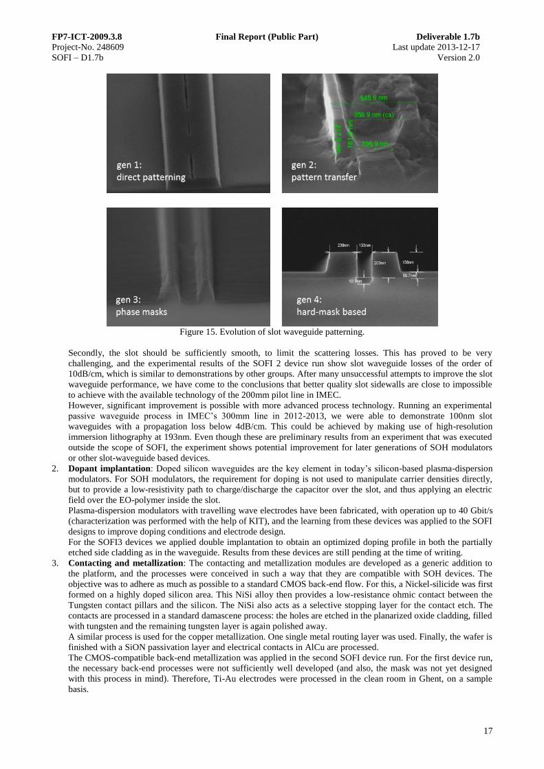
1. Slot waveguide patterning: Efficient SOH modulators require low-loss slot waveguides. There are two main
challenges in making good slot waveguides. First of all, the slot should be sufficiently narrow, i.e. ~100nm or less.
This is a very aggressive feature for the optical lithography used in IMEC’s 200mm line. In the SOFI project,
IMEC experimented with several techniques to achieve such narrow slot waveguides: pattern transfer and phase-
shift masks did not work. In the end, the introduction of a hard mask solved the problem. This process was carried
and over from a parallel development to improve the future integration of active devices and tuned to yield 100nm
slot waveguides. The results of the different processes are shown in the pictures below.
FP7-ICT-2009.3.8 Final Report (Public Part) Deliverable 1.7b
Project-No. 248609 Last update 2013-12-17
SOFI – D1.7b Version 2.0
17
Figure 15. Evolution of slot waveguide patterning.
Secondly, the slot should be sufficiently smooth, to limit the scattering losses. This has proved to be very
challenging, and the experimental results of the SOFI 2 device run show slot waveguide losses of the order of
10dB/cm, which is similar to demonstrations by other groups. After many unsuccessful attempts to improve the slot
waveguide performance, we have come to the conclusions that better quality slot sidewalls are close to impossible
to achieve with the available technology of the 200mm pilot line in IMEC.
However, significant improvement is possible with more advanced process technology. Running an experimental
passive waveguide process in IMEC’s 300mm line in 2012-2013, we were able to demonstrate 100nm slot
waveguides with a propagation loss below 4dB/cm. This could be achieved by making use of high-resolution
immersion lithography at 193nm. Even though these are preliminary results from an experiment that was executed
outside the scope of SOFI, the experiment shows potential improvement for later generations of SOH modulators
or other slot-waveguide based devices.
2. Dopant implantation: Doped silicon waveguides are the key element in today’s silicon-based plasma-dispersion
modulators. For SOH modulators, the requirement for doping is not used to manipulate carrier densities directly,
but to provide a low-resistivity path to charge/discharge the capacitor over the slot, and thus applying an electric
field over the EO-polymer inside the slot.
Plasma-dispersion modulators with travelling wave electrodes have been fabricated, with operation up to 40 Gbit/s
(characterization was performed with the help of KIT), and the learning from these devices was applied to the SOFI
designs to improve doping conditions and electrode design.
For the SOFI3 devices we applied double implantation to obtain an optimized doping profile in both the partially
etched side cladding as in the waveguide. Results from these devices are still pending at the time of writing.
3. Contacting and metallization: The contacting and metallization modules are developed as a generic addition to
the platform, and the processes were conceived in such a way that they are compatible with SOH devices. The
objective was to adhere as much as possible to a standard CMOS back-end flow. For this, a Nickel-silicide was first
formed on a highly doped silicon area. This NiSi alloy then provides a low-resistance ohmic contact between the
Tungsten contact pillars and the silicon. The NiSi also acts as a selective stopping layer for the contact etch. The
contacts are processed in a standard damascene process: the holes are etched in the planarized oxide cladding, filled
with tungsten and the remaining tungsten layer is again polished away.
A similar process is used for the copper metallization. One single metal routing layer was used. Finally, the wafer is
finished with a SiON passivation layer and electrical contacts in AlCu are processed.
The CMOS-compatible back-end metallization was applied in the second SOFI device run. For the first device run,
the necessary back-end processes were not sufficiently well developed (and also, the mask was not yet designed
with this process in mind). Therefore, Ti-Au electrodes were processed in the clean room in Ghent, on a sample
basis.

FP7-ICT-2009.3.8 Final Report (Public Part) Deliverable 1.7b
Project-No. 248609 Last update 2013-12-17
SOFI – D1.7b Version 2.0
18
Both the Cu/AlCu back-end, as well as the Ti-Au electrodes performed well and offered sufficiently high
bandwidth for modulator operation well beyond 40 Gbps.
4. Back-end opening: Because the electro-optic polymers cannot be inserted during the processing of the slot, the
waveguides need to be exposed again after the wafer has gone through the entire back-end metallization and
passivation. This is not a trivial step, because there is no selective stop layer at the waveguide level to ensure the
exact amount of cladding oxide is removed.
For the SOFI1 devices, a non-CMOS backend was processed, and the slots were protected with a polymer to ensure
they could easily be opened after the electrode processing.
For the SOFI2 devices, the BEOL opening process was conducted in two stages: First, a dry etch was applied at
wafer scale, and the remaining thickness was mapped over the entire wafer. Then the wafer was diced. Based on
the thickness map, the individual samples were etched in the Ghent or KIT clean room with a timed HF etch. Loss
measurements on modulator devices show that there is no significant impact on the waveguide quality because of
this process, if timed correctly and an under-etch is avoided.
For the SOFI3 devices, this process is adapted for wafer scale processing in imec. At the time of writing, the
development is ongoing, and a dedicated wafer batch has been assigned for this development. A critical challenge
in this development is avoiding the undercut in the slot.
The result of these different process modules is shown in the SEM pictures below: the slot waveguide in the center,
sitting in an etched trench in the backend, where the copper and tungsten metallization is visible.
Figure 16. Strip-loaded slot waveguide exposed by back-end opening.
During the project, IMEC manufactured 3 batches of SOH devices, with increasing levels of complexity, both in design
(mainly by KIT) and in process flow. While the manufacturing runs have suffered from serious delays, the resulting
devices performed well on most accounts.
3.5 SOH functionalization To equip passive silicon structures produced according to the methods present above, an organic cladding has to be
added to “functionalize” (= add its new function) the waveguides and provide them with unique and superior properties
not available from the pure SOI platform.
Rainbow Photonics selected and synthesized the best EO organic crystals known up to date. With these materials, two
different deposition approaches have been investigated: solution growth and melt growth. We have shown that melt
growth is much more compatible with silicon nanostructures requiring filling of silicon slot waveguides, therefore melt
growth has been optimized for different materials and substrates considering seeding conditions, growth temperatures,
temperature gradients and cooling rates to control the growth rates on differently structures SOI substrates.
The details of the deposition parameters depend on the particular material and may also vary depending on the chip
type, i.e. wetting properties of the chip, which depend on the fabrication procedures prior to organic material deposition,
in our case the fabrication procedures of the passive SOI structures by IMEC. Besides wetting properties, the deposition
of organic crystals is obviously also affected by the geometry of the structures, for example by the depth and by the
orientation of the trenches. However, the general growth procedure developed does not change considerably and is
described below for the particular case of BNA material. With other materials, the main difference is the growth

FP7-ICT-2009.3.8 Final Report (Public Part) Deliverable 1.7b
Project-No. 248609 Last update 2013-12-17
SOFI – D1.7b Version 2.0
19
temperature (e.g., for OH1 it is above 200 ºC), seeding conditions (for OH1 only one heating cycle is used instead or
two as best for BNA) and growth direction: with BNA it is optimal to grow the crystal along the waveguide direction,
while for OH1 perpendicular to it.
The alignment of the optical axis of the organic crystal of BNA created on-chip can be verified with a reflection
microscope by placing and rotating the sample between crossed polarizers relying on the birefringence of BNA, see .
The achieved crystalline orientation is only approximately close to the optimal direction, which is because the growth
direction was not restricted enough in the ac-plane, respectively xz-plane. (a) illustrates a deviation from the optimum
by 15º. (b) shows the chip used for the data generation experiment by KIT. Its polar axis is 34° off the ideal direction.
Additional growth-guiding trenches in unused regions of the chip or the cover glass could optimize this step, since for
well-defined micro-size channels the growth direction is always perfectly aligned [9].
Figure 17. Microscope images of details on SOI chips (SOFI2-CMOS metal stack) covered with BNA single crystal
between crossed polarizers utilizing the birefringence of the cladding BNA material. In case (a), the crystal is oriented
about 15º from the optimal direction with the polar axis c normal to the WGs, while in case (b) this angle is about 34º.
In both cases one single crystalline domain across multiple MZMs has been achieved.
In summary, we have been developed new melt deposition techniques for organic crystals to enable EO functionality of
silicon waveguides. This we demonstrated using high-speed amplitude modulation at 12.5 Gbit/s in an SOH Mach-
Zehnder device utilizing a single crystalline organic film.
GigOptix-Helix (GO) Related to the objective of identifying electro-optic polymers for operations at 85°C and high
electro-optic coefficient (>100 pm/V at 1.55 μm light wavelength) suitable for use within SOFI, GO monitored the
evolution of the GigOptix-Bothell electro-optic material. GO coordinated the intense exchange of sample material and
work instructions between GigOptix Bothell (supplier to the consortium) and KIT.
Bonding the modulators by flip chip requires a temperature around 100°C. The M1 polymer from GO has a glass
transition temperature Tg of 138°C. It is expected that the polymer properties degrade during flip chip bonding. GO has
developed a new polymer M3, which has a higher Tg of 167°C, but also a higher optical loss (1.3 dB/cm instead of
1 dB/cm). GO provided the new polymer to KIT and KIT successfully poled the material.
3.6 Packaging of SOH devices The SOFI project relies on vertically coupled SOI optical devices. Facing this issue, SELEX found a procedure
enabling a stable chip to fiber alignment and fastening. The solution was to extend the contacting area of the fiber by
the use of zirconium capillaries. Gluing the contact interfaces between the fiber and the SOI substrate results in a stable
assembly.
A specific tool for fiber alignment and pigtailing has been designed and realized (see Figure 18). It consists of suitable
fiber holders, stages for movement, support capillaries and polarization maintaining fibers. The fiber capillary is
polished at an angle of 10° for an optimized optical coupling with the grating.

FP7-ICT-2009.3.8 Final Report (Public Part) Deliverable 1.7b
Project-No. 248609 Last update 2013-12-17
SOFI – D1.7b Version 2.0
20
Figure 18. Tools for fiber alignment and pigtailing.
The first results of the fiber pigtailing were obtained with the chips coming from the SOFI1 run. Optical losses between
6.8 dB and 10 dB have been reported in 3mm long straight waveguides sampled from the wafer D07, D11 and D12 (see
Figure 19). This includes two grating couplers which have 3 dB loss each, in the very best case.
One structure from the wafer D12, consisting on a longer curved waveguide (5.5mm) has been also pigtailed and
electrically connected on a test carrier sample. The losses experienced are 14 dB.
Figure 19. Polarization maintaining fiber glued on SOFI1 chip. Losses range from 6.8 dB to 10 dB for 3 mm straight
waveguides, including 2 grating couplers. A longer curved waveguides (5.5 mm) has been also packaged in a chip
carrier and electrically wired (optical losses 14 dB).
Several approaches have been investigated in order to connect the SOI input electrode to a standard input connector.
The proposed final method consists of the flip-chip approach (see Figure 20). It has been chosen to reduce the wiring
length as well as the RF losses and the related inductance.
The flip-chip approach is also more suitable for the industrialization of the connection procedure. For this aim, a
suitable package has been realized. Considered the novelty of this approach, as well as the need to finalize a prototype,
the package has been designed as flexible as possible, in order to allow for both flip-chip and standard wiring.

FP7-ICT-2009.3.8 Final Report (Public Part) Deliverable 1.7b
Project-No. 248609 Last update 2013-12-17
SOFI – D1.7b Version 2.0
21
Figure 20: Flip-chip package, design (Si-chip in blue, alumina chip in white) and realization.
The main packaging difficulties stem from the integration of the SOI chip with the organic polymers that is used for the
electro optic features.
In fact, on one side the flip-chip method is hard to realize (the polymer on the top of the chip avoids both electrical
contacting between the SOI electrodes and the bumps, which serve as a fastening between SOI chip and the alumina
substrate). On the other side, if standard wiring is exploited, the UV light used for fiber gluing damages the polymer (in
the case of flip chip the alumina shadows the polymer).
3.7 SOH modulator characterization and benchmarking SOH modulators have been characterized in the labs of KIT. Several subcomponents have been developed for this
purpose.
A strip-to-slot waveguide converter was simulated, realized and characterized, see Figure 21. The work was published
as [10].
Figure 21. Simulation of a strip-to-slot waveguide converter. (a) Topview with electric field distribution in the
logarithmically tapered strip-to-striploaded slot mode converter. (b) Transmission and reflection factors.
Image source: [10].
SOH MZMs and SOH IQ modulators have been built following the concept shown in the next figure. Two nested
MZMs constitute one IQ modulator. The phase modulator sections in each MZM are the strip-loaded socket
waveguides. The slots are filled with the nonlinear material.

FP7-ICT-2009.3.8 Final Report (Public Part) Deliverable 1.7b
Project-No. 248609 Last update 2013-12-17
SOFI – D1.7b Version 2.0
22
Figure 22. IQ modulator based on the SOH concept. (a) Topview of the IQ modulator with nested Mach-Zehnder
modulators (MZM), displaying optical waveguides (WG) in blue and electrical lines in orange. (b) Cross section of an
SOH MZM, showing two silicon striploaded slot WGs, which act as phase shifters. They are filled and covered with a
nonlinear cladding (not shown for clarity). The coplanar RF transmission line (GSG, ground-signal-ground) is
impedance matched to the driving signal generator. The RF voltage at the S-electrode creates oppositely directed
electric slot fields (red arrows). During the fabrication process, the χ(2)-nonlinearity is created by applying a poling
voltage between both RF ground (G) electrodes at an elevated temperature. This aligns (poles) the active cladding
molecules in a direction indicated by green arrows. In combination with the poled cladding, the modulating RF voltage
leads to opposite phase shifts in both interferometer arms. (c) Color-coded dominant x-component |Ex| of the optical
electrical field in the slot WG cross section. (d) Modulating electrical RF field. Both fields are strongly confined to the
slot, resulting in high modulation efficiency. Figure source: [1].
To make SOH modulators, this concept has been implemented by making use of a CMOS like metal stack as shown in
the next figure. The results stem from a 2nd
generation SOFI device.
Figure 23. Detailed cross section of MZM as implemented, showing two phase modulators with striploaded slot WGs,
filled with nonlinear cladding; not to scale. Rails are connected to ground-signal-ground electrodes by tungsten vias, a
silicide layer and the Si striploads. This electrode arrangement allows crossings of optical WGs and electrical
transmission lines. Furthermore, it corresponds to the first part of standard metal stacks as known from CMOS
technology. Figure source: [1].
A data generation experiment at 28 GBd using QPSK and 16QAM reaching 112 Gbit/s confirmed that this device
with a length of 1.5 mm performs well within the limits of standard forward error correction (FEC), see Figure 24. The
polymer produced by GigOptix called M3 has been used in this experiment.

FP7-ICT-2009.3.8 Final Report (Public Part) Deliverable 1.7b
Project-No. 248609 Last update 2013-12-17
SOFI – D1.7b Version 2.0
23
Figure 24. Data generation on a single channel and polarization with SOH IQ modulator at 28 GBd detected using post-
equalization with 19-taps. Error free operation is measured and displayed in (a) constellation and (b, c) eye diagrams.
(d) Constellation and (b, c) eye diagrams as observed when employing an 8-tap (1 tap per symbol) pre-emphasis at the
transmitter, and no equalization at the receiver. The BER is 1.2 × 10⁻³
, and the EVM is 10.3%. Figure source: [1].
Energy efficiency: Switching to a new, experimental polymer improved the voltage-length product considerable and is
a nice example illustrating the SOH concept. “Simply” find a new cladding and a device can be considerably improved,
whereas pure SOI modulators require iterative optimization. The resulting low voltage length product allows ultra-low
drive voltages [11].
Comb line generation is another task well suited to SOH MZMs, due to their low drive voltages. These frequency
combs can be used to create OFDM signals all-optically on-chip. An intermediate step to verify was to create a comb
with a larger spacing (and incidentally generating a comb with properties of interest to SELEX) to do wavelength
division multiplexing (WDM). The next figure illustrates that a data signal of 784 Gbit/s can be generated as follows:
(a) Use an SOH dual-drive MZM of 2 mm length operated at 40 GHz to create a frequency comb with 40 GHz spacing.
(b) Encode with an LN modulator the same 28 GBd QPSK signal on each carrier.
(c) Separate into even and odd channels, and decorrelate these channels.
(d) Appling an polarization multiplexing.
(e) Receive using an optical modulation analyzer (OMA).
Figure 25. Data transmission setup after generation of comb with SOH MZM: Each comb line is modulated with a
28 GBd QPSK signal. Even and odd channels are separated with a wavelength-selective switch (WSS) to decorrelate
neighboring channels. Both data streams are merged and are polarization multiplexed (PolMUX). After amplification,
the channels are demultiplexed and detected by an optical modulation analyzer (OMA) and a tunable laser acting as a
local oscillator (LO). Figure source: [4]

FP7-ICT-2009.3.8 Final Report (Public Part) Deliverable 1.7b
Project-No. 248609 Last update 2013-12-17
SOFI – D1.7b Version 2.0
24
The viability of using an SOH comb line generator for WDM is proven in the next figure, which shows that each
channel can be transmitted with an EVM within the limits of standard FEC.
Figure 26. Frequency comb generated by SOH modulator to do WDM using a LN modulator: Data transmission of
784 Gbit/s using QPSK signals on 7 carriers generated by an integrated SOH comb source. Comb spectrum (left) and
constellation diagrams for all channels and both polarization are depicted along with measured EVM values. BER
below hard-decision threshold are achieved for all signals. Figure source: [4]
The characterization of SOH modulators together with design and simulation generated numerous publications and also
prompted KIT to start 2 patent applications focusing on increasing modulation speed by enhancing the modulator’s RC
constant. The applications are listed here:
‘Electro-optical device and method for processing an optical signal, EU,’ L. Alloatti, J. Leuthold, W. Freude, C. Koos,
D. Korn, and R. Palmer, EP 11003562.3-1228 (2012).
‘Electro-optical device and method for processing an optical signal, USA,’ L. Alloatti, J. Leuthold, W. Freude, C. Koos,
D. Korn, and R. Palmer, U.S.A. 13/460,395 (2012).
Benchmarking studies were extended to real experimental measurements using research prototypes developed under
the FP7 project GALACTICO as a reference. A number of GaAs chips provided by the GALACTICO consortium were
measured at KIT facilities by KIT and AIT researchers to compare their performance with the SOFI modulators. A
3 dB bandwidth of about 32 GHz and constellation diagrams for up to 64QAM modulation at 25 GBd were obtained.
Although GaAs devices delivered better results in terms of modulation quality, it is hard to draw conclusions without
defining the desired balance with other important devices characteristics, such as foot print and integrability with further
functionality on chip (electronics, making arrays). This will require further study outside the SOFI project.
Figure 27. Constellation diagrams generated by KIT and AIT with the GALACTICO GaAs IQ modulators. Figure
source: [12].
3.8 Driver solution for SOH modulators GigOptix-Helix AG, a leading fabless supplier of semiconductor components for optical interconnects and CE
applications, is a wholly owned subsidiary of GigOptix, Inc (GigOptix), which is serving the wider market of high
speed data streaming and telecommunications with a broad offering of semiconductor and optical components.
GigOptix has developed and produces Telcordia proven electro-optical polymer materials which GigOptix used to
develop optical modulators addressing all relevant applications in optical transport, including DPSK, RZ-DQPSK, DP-
QPSK and 16QAM with speed up to 100 Gbit/s with OOK and 200 Gbit/s with 16QAM. GigOptix-Helix focuses on
chipset for optical interconnect with single channel, quad channels and twelve channels VCSEL drivers and TIA w post
amp with channel speed up to 28 Gbit/s and are currently used mainly in MMF optical links for datacentres. The

FP7-ICT-2009.3.8 Final Report (Public Part) Deliverable 1.7b
Project-No. 248609 Last update 2013-12-17
SOFI – D1.7b Version 2.0
25
receiver arrays have been recently massively introduced in 40 Gbit/s ER and LR links in response to the request from
the market for higher level of integration and power dissipation reduction.
The SOFI project aims to implement a silicon-organic hybrid platform which allows for very compact modulators
capable of high speed operations and that can be operated in linear mode. These features make the SOFI modulators of
potential great interest to GigOptix for standalone use into TOSAs for metro and client side links. Moreover, the
possibility of monolithic CMOS integration of the driving electronics with the modulator may make the SOH approach
suitable for deployment of EO systems in CE, an area in which GigOptix-Helix in particular is already active.
Figure 28. Applications space for GigOptix products.
GigOptix is present in the target applications space with the following optics related products:
- Drivers for EO modulators. Single channel to 4 channels, bit rate per channel up to 32 Gbit/s. SMT, GPPO or
coplanar interfaces. Used in 10G to 400G optical transport transmitters.
- MZ modulators. Single and nested MZ modulators, also dual polarization. Used in DPSK, RZ-DQPSK, DP-
QPSK and 16QAM with speed up to 100 Gbit/s with OOK and 200 Gbit/s with 16QAM.
- TIAs for coherent receivers. Linear, dual channel, integrated VGA stage with PLD, TIA gain and BW control.
Up to 32 Gbit/s per channel. Used in 100G and above coherent receivers.
- VCSEL drivers. Single channel, quad channels, twelve channels with speed up to 28 Gbit/s per channel. Used
in transmitter side of optical interconnects.
- Limiting TIA Arrays with post-amp. Single channel, quad channels, twelve channels with speed up to
28 Gbit/s. Used in receiver side of optical interconnects and receivers for client side optical interfaces.
- Specialized TIAs for 3D cameras.
Within the continuous efforts to ever increase networks capacity and speed, the following trends have been identified:
- Long Haul Optical Transport. The increase in capacity and speed is a primary value and accelerated innovation
is pursued in some cases at the expense of integration and cost. This approach is justified by the relatively
small volumes (10Ks/Y units for the highest speed optical transport interfaces at any given time) and the
benefit OEMs have by releasing to the market new products – since this somewhat drives CAPEX on the
operators side.
- METRO. Due to the significantly larger volumes with respect to LH/ULH, focus is on the most cost effective
solutions, which includes consideration of small foot print and low power dissipation. The increase in
performance is achieved through optimization of technology which had become legacy in LH/ULH or
adapted from other application areas.
GigOptix worked on the study for an integrated driver. In a first step the SiGe and CMOS technologies were compared
based on the transit frequency ft. The required transit frequency for a 25 Gbit/s driver is above 200 GHz. The slowest
BiCMOS technology which fulfills the requirements is a 120 nm BiCMOS process. For the CMOS-only case, a 40 nm
technology has to be chosen.
The BiCMOS process has lower mask costs (~300 k$), but higher variable costs per chip, while the CMOS process has
much higher mask costs (~2 M$), but lower variable costs per chip.

FP7-ICT-2009.3.8 Final Report (Public Part) Deliverable 1.7b
Project-No. 248609 Last update 2013-12-17
SOFI – D1.7b Version 2.0
26
Figure 29. Comparison of the total costs for a certain number of produced chips.
From a cost perspective, SiGe is the better suited technology if less than 10 Mio chips are sold.
Furthermore, the 120 nm BiCMOS process can operate with higher supply voltages than the 40 nm CMOS process. A
higher supply voltage (around 3.3 V) enables higher swing sizes.
In order to test the capability to drive a modulator with a SiGe driver, GO worked on an evaluation board. For the
evaluation board, a prototype trans-impedance amplifier (TIA) with integrated limiting amplifier from GO has been
used. The TIA has normally a current input and is directly bonded to a photo diode (PD). The evaluation board was
modified, so that a single ended electrical signal can be fed to the TIA. Because the chip has a very high
transimpedance, the electrical signal has to be attenuated between the pattern generator and the board.
Figure 30. Evaluation board for the 25 Gbit/s driver with electrical input and electrical output.
The chip has an I2C interface. The main settings of the chip can be controlled from a PC with a GUI, these settings
include the output swing and pre-emphasis.
GO measured output swings up to 600mV. The eye is not fully open. The measured jitter is mainly limited by the
measurement setup. The evaluation board has been shipped to KIT and KIT verified the electrical performance and
were able to drive a polymer modulator.

FP7-ICT-2009.3.8 Final Report (Public Part) Deliverable 1.7b
Project-No. 248609 Last update 2013-12-17
SOFI – D1.7b Version 2.0
27
Figure 31. Measured single ended eye diagram at 20 Gbit/s. The measurement was limited by the measurement setup
and its limited jitter performance.
In the meantime, an improved version of this prototype chip was designed. The new version should have more
bandwidth, improved pre-emphasis and channel inversion. The device was successfully characterized by GigOptix.
On SOFI3 run, KIT designed an array of IQ modulators with 4 QPSK channels. The electrodes have the same spacing
as our 12 channel prototype chip. The aim is to directly bond the driver chip to the MZMs and drive all 8
simultaneously at 25 Gbit/s or 12.5 Gbit/s. In order to do this, GO started with the design of a dedicated EVB.
Figure 32. Sketch of the dedicated PCB to drive the 8 MZM
Figure 33. Integration Trend for METRO optical interfaces.
In particular METRO applications are calling for DP-QPSK modulators with small footprint, low Vpi, BW capable of
28 GBd to 32 GBd. Possibility to integrate the drivers with the modulator is considered a plus. In the future, to extend
further the capacity, there may be need to support complex modulation formats, like 16QAM also, which will call for
modulators capable of linear operations. All the above requirements are among the targets of SOFI and supporting the
interest at GigOptix in the SOFI project.

FP7-ICT-2009.3.8 Final Report (Public Part) Deliverable 1.7b
Project-No. 248609 Last update 2013-12-17
SOFI – D1.7b Version 2.0
28
Another relevant use case for the components and technologies developed in SOFI is the emerging need for high speed
links for the campus and very large datacenters. Until recently the size of datacenters was such that the vast majority of
links was below 30 m with very few links of 100 m and above and maximum length of 300 m. Such requirements
allowed for the implementation of optical links for datacenters using MMF and 850 nm VCSELs. Due to the great
increase in size of datacenters and the introduction of new network architectures to improve the speed and reliability of
the datacenters operations, the requirement for 1 km to 2 km links has recently emerged. Current implementations for
such links are based on OOK and CWDM, however such solutions are offering between 40 Gbit/s and 100 Gbit/s with
a path to 400G that can be achieved only increasing the complexity of the optics. Following successful commercial
introduction of ultrafast DAC it is being proposed to use multilevel amplitude signaling (8PAM or 16PAM) to increase
the capacity for this class of optical links. This application requires the MZ modulator to operate in linear mode driven
by DSP generated signals. The electronic needed to generate the transmitted signal would include high complexity large
real estate mixed signal circuitry with significant size/cost benefits coming from the monolithic CMOS integration of
the electronics with the optical modulators, one of the main investigation areas of the SOFI project.
Very large volume deployment of optical links in consumer electronics has not happened yet but there are ever growing
indications it will happen soon. 10 Gbit/s and 20 Gbit/s serial links to connect the PC to external peripherals have been
already proposed by leading manufacturers (APPLE/INTEL, Thunderbold) and the extension of existing PC interfaces
to support optical physical layer (USB and PCIe) is ongoing. For these applications, for which annual volumes of tenths
of millions devices per year are likely and cost will need to reach the level of a few $s per port, monolithic integration
of CMOS electronics with the E/O components looks attractive.
To summarize, GigOptix interest related to the SOFI project is manifold and relates to a number of the market GigOptix
is active in. The most relevant aspects in SOFI as far as GigOptix is concerned are:
- The development of a technology yielding very compact and complex modulators capable of high speed
operations and that can be operated in linear mode.
- The monolithic CMOS integration of the transmitter electronics with the modulator.
4 Potential impact It is now widely recognized that reducing the level of global energy consumption is of paramount importance and must
be addressed with urgency. Silicon photonic technologies and more specifically silicon hybrid technologies offer
significant advantages towards achieving this goal. Currently, the total energy required to power the Internet, including
data centers, network nodes and user terminals, amounts to about 4% of today’s electricity generation. With Internet
traffic doubling every 18 months, a 64-fold increase in the Internet’s total power consumption is expected in less than
10 years, and this would require a more than doubling of the required total capacity for global electricity generation.
In accordance to the above, the EU’s climate and energy policy has set a target for cutting energy consumption by 20%
of projected 2020 levels by improving energy efficiency. Information and Communication Technologies (ICT) play a
key role in the roadmap strategy towards reduction of carbon footprint in assisting the performance of other sectors in
the world economy. However, in recent years the carbon emissions of ICT itself have rapidly increased due to the
associated growth of internet traffic owing to social networking and video services which at the end of 2012 will
account for more than half of the global internet traffic. Despite the fact that, at the current capacity levels
telecommunication networks power consumption is at moderate values, the forecasted traffic growth predicts that in the
upcoming years it will become a major problem for the operators strategic planning.
The studies of AIT show that SOH will be a competitive modulator technology that is capable to meet the specifications
of new generation long haul and access networks, which will require high speed modulators with ultra-high bandwidth,
i.e., modulators showing superior performance with respect to commercial available technologies (e.g LiNbO3), low
power consumption and at reduced cost. Extended analyses and a number of simulations show that a total network
energy lowering in the order of 22% is achievable using the SOFI devices leading to new more efficient subsystems and
meeting the EU requirements for greener technologies.
From IMEC’s point of view, the direct impact of the project is a significant enhancement of the technology platform:
The incorporation of high-quality exposed slot waveguides in a CMOS-compatible silicon photonics platform is not
only relevant for high-speed and low-power modulators, but also for sensors. This can be a key differentiator of silicon
photonics.
As one of the technology providers for ePIXfab, IMEC has also recently started to offer the full platform (passives +
modulators + detectors) in multi-project wafer (MPW) runs. The SOFI-specific modules are not yet a part of that

FP7-ICT-2009.3.8 Final Report (Public Part) Deliverable 1.7b
Project-No. 248609 Last update 2013-12-17
SOFI – D1.7b Version 2.0
29
offering, but if there is a clear demand for back-end opening, IMEC will consider to integrate this as a standard module
in the platform. This injects the SOFI technology into the silicon photonics supply chain in Europe.
Within the SOFI project, silicon-organic hybrid modulation at a high speed has been demonstrated for the first time
with organic crystals from Rainbow Photonics. This opens up a new opportunity for organic crystals to replace poled
polymers in SOH applications where high long-term stability, resistance to high optical powers and temperatures, and
parallelism is required, (for polymers it is difficult to pole several on-chip devices simultaneously). This is not only
interesting for high-speed electro-optic modulation, but also other applications where high-speed (2) nonlinear optical
functionality is required. For example, organic electro-optic crystals are very promising for THz-wave generation in a
broad range 0.1–20 THz and above, presently used exclusively in a bulk form by several research groups worldwide
and in commercial THz sources offered by Rainbow Photonics. The integrated SOH platform could offer more than
three orders of magnitude better optical-to-THz conversion efficiencies compared to present (bulk) applications,
considerably reduced size compatible with applications such as endoscopy and THz micro-testing, as well as new
functionalities offered by silicon structures.
Many commercial products prove that it is possible to design chromophores hosted polymers for durable, resilient
products. In the SOFI project the material M3 of GigOptix Inc. has been used to produce SOH modulators. This is the
very same material employed in Telecordia certified modulators sold by GigOptix. Also new polymers/chromophores
can be further enhanced. Demand for high performing, energy efficient modulators will drive these developments in
chemistry.
The potential applications from the output of the project envisaged by SELEX ES rely on both military and civil fields
that are mainly focused on the improvement of advanced generation of Multifunction Phased Array Radars (M-PAR).
The SOH modulator developed in SOFI is a useful building block to be used within already existing products as well as
for future RADAR architecture.
It has been identified as a potential replacement for the modulators based on other technologies (such as LiNbO3, GaAs,
GaN, Si EAM) in both analogue and digital optical links, with the advantages of increased bandwidth, power efficiency,
scalability, and reduced volume and costs.
In SOFI, GigOptix-Helix performed a study for an optimized driver for the SOFI modulator. Also, the feasibility of
driving a SOFI modulator with an integrated Silicon-Germanium (SiGe) driver was proved. This result is of particular
relevance since the possibility to drive the SOFI modulator with SiGe drivers may allow the deployment of the SOFI
modulators even in cases in which the volumes do not justify the investment in the monolithic integration of the
electronics with the modulator. Also the possibility to use compact low power SiGe drivers still support extremely
compact low power multi-channel TOSAs in which the SOFI modulators shall provide a distinct advantage with respect
to competing technologies.
Support in the design activities and process developments for the SOFI modulator. It is worth mentioning that the
material supplier by GigOptix-Helix allowed an early validation of the SOFI concept and proved to be well suited for
the realization of complex optical components on silicon optical waveguides, like the SOFI IQ modulator.
The SOFI project helped to establish that SOH modulators and SOH photonic integrated circuits support advanced
modulation formats, provide exceptionally high bandwidth, also because devices can be made especially short thanks to
very low VL products. Moreover by using modulators of 1 mm length this modulation efficiency translates into the
most energy efficient high-speed Mach-Zehnder modulators to-date, which are not bound to a specific, hard to control
wavelength.

FP7-ICT-2009.3.8 Final Report (Public Part) Deliverable 1.7b
Project-No. 248609 Last update 2013-12-17
SOFI – D1.7b Version 2.0
30
References
These are selected SOFI publications used for illustration above.
[1] D. Korn, R. Palmer, H. Yu, P. C. Schindler, L. Alloatti, M. Baier, R. Schmogrow, W. Bogaerts, S. K. Selvaraja, G.
Lepage, M. Pantouvaki, J. M. D. Wouters, P. Verheyen, J. Van Campenhout, B. Chen, R. Baets, P. Absil, R. Dinu,
C. Koos, W. Freude, and J. Leuthold, “Silicon-organic hybrid (SOH) IQ modulator using the linear electro-optic
effect for transmitting 16QAM at 112 Gbit/s,” Opt. Express, vol. 21, no. 11, pp. 13219–13227, Jun. 2013.
[2] J. Leuthold, C. Koos, W. Freude, L. Alloatti, R. Palmer, D. Korn, J. Pfeifle, M. Lauermann, R. Dinu, S. Wehrli, M.
Jazbinsek, P. Gunter, M. Waldow, T. Wahlbrink, J. Bolten, H. Kurz, M. Fournier, J.-M. Fedeli, H. Yu, and W.
Bogaerts, “Silicon-Organic Hybrid Electro-Optical Devices,” IEEE J. Sel. Top. Quantum Electron., vol. 19, no. 6,
pp. 3401413–3401413, 2013.
[3] R. Palmer, L. Alloatti, D. Korn, P. C. Schindler, M. Baier, J. Bolten, T. Wahlbrink, M. Waldow, R. Dinu, W.
Freude, C. Koos, and J. Leuthold, “Low power Mach-Zehnder modulator in silicon-organic hybrid technology,”
IEEE Photonics Technol. Lett., vol. 25, no. 13, pp. 1226–1229, 2013.
[4] C. Weimann, S. Wolf, D. Korn, R. Palmer, S. Koeber, R. Schmogrow, P. C. Schindler, L. Alloatti, A. Ludwig, W.
Heni, D. Bekele, D. L. Elder, H. Yu, W. Bogaerts, L. R. Dalton, W. Freude, J. Leuthold, and C. Koos, “Silicon-
organic hybrid (SOH) frequency comb source for data transmission at 784 Gbit/s,” 39th Eur. Conf. Exhib. Opt.
Commun. ECOC, no. Th.2.B.1, 2013.
[5] J. Pfeifle, L. Alloatti, W. Freude, J. Leuthold, and C. Koos, “Silicon-organic hybrid phase shifter based on a slot
waveguide with a liquid-crystal cladding,” Opt. Express, vol. 20, no. 14, pp. 15359–15376, Jul. 2012.
[6] D. Korn, M. Lauermann, P. Appel, L. Alloatti, R. Palmer, W. Freude, J. Leuthold, and C. Koos, “First Silicon-
Organic Hybrid Laser at Telecommunication Wavelength,” in CLEO: Science and Innovations, 2012, p. CTu2I.1.
[7] M. Lauermann, D. Korn, P. Appel, L. Alloatti, W. Freude, J. Leuthold, and C. Koos, “Silicon-Organic Hybrid
(SOH) Lasers at Telecommunication Wavelengths,” in Advanced Photonics Congress, 2012, p. IM3A.3.
[8] L. Alloatti, D. Korn, C. Weimann, C. Koos, W. Freude, and J. Leuthold, “Second-order nonlinear silicon-organic
hybrid waveguides,” Opt. Express, vol. 20, no. 18, pp. 20506–20515, Aug. 2012.
[9] M. Jazbinsek, H. Figi, C. Hunziker, B. Ruiz, S.-J. Kwon, O.-P. Kwon, Z. Yang, and P. Günter, “Organic electro-
optic single crystalline films for integrated optics,” presented at the Linear and Nonlinear Optics of Organic
Materials X, San Diego, California, USA, 2010, p. 77740Q–77740Q–10.
[10] R. Palmer, L. Alloatti, D. Korn, W. Heni, P. C. Schindler, J. Bolten, M. Karl, M. Waldow, T. Wahlbrink, W.
Freude, C. Koos, and J. Leuthold, “Low-Loss Silicon Strip-to-Slot Mode Converters,” IEEE Photonics J., vol. 5,
no. 1, pp. 2200409–2200409, 2013.
[11] R. Palmer, S. Koeber, W. Heni, D. L. Elder, D. Korn, H. Yu, L. Alloatti, S. Koenig, P. C. Schindler, W. Bogaerts,
M. Pantouvaki, G. Lepage, P. Verheyen, J. Campenhout, P. Absil, R. Baets, L. R. Dalton, W. Freude, J. Leuthold,
and C. Koos, “High-Speed Silicon-Organic Hybrid (SOH) Modulator with 1.6 fJ/bit and 180 pm/V In-Device
Nonlinearity,” presented at the ECOC 2013, London, UK, 2013, p. We.3.B.3.
[12] D. Korn, P. C. Schindler, C. Stamatiadis, M. F. O’Keefe, L. Stampoulidis, R. M. Schmogrow, P. Zakynthinos, R.
Palmer, N. Cameron, Y. Zhou, R. G. Walker, E. Kehayas, I. Tomkos, L. Zimmermann, K. Petermann, W. Freude,
C. Koos, and J. Leuthold, “First monolithic GaAs IQ electro-optic modulator, demonstrated at 150 Gbit/s with 64-
QAM,” in Optical Fiber Communication Conference/National Fiber Optic Engineers Conference 2013, 2013, p.
PDP5C.4.

FP7-ICT-2009.3.8 Final Report (Public Part) Deliverable 1.7b
Project-No. 248609 Last update 2013-12-17
SOFI – D1.7b Version 2.0
31
5 Use and dissemination of foreground – Section A (dissemination measures, scientific publications) This chapter is also implemented as deliverable D6.7, D6.8, D6.10 and reproduced here to make this a standalone document.
A1: LIST OF SCIENTIFIC (PEER REVIEWED) PUBLICATIONS, STARTING WITH THE MOST IMPORTANT ONES
NO. Title Main
author
Title of the
periodical or
the series
Number, date or
frequency Publisher
Place of
publication
Year of
publication
Relevant
pages
Permanent identifiers[1]
(if available)
Is/Will
open
access[2]
provided to
this
publication?
1 ‘Silicon-organic hybrid
(SOH) IQ modulator using
the linear electro-optic effect
for transmitting 16QAM at
112 Gbit/s’
KIT Optics Express 2013 doi: 10.1364/OE.21.013219 yes
2 Low Power Mach-Zehnder
Modulator in Silicon-
Organic Hybrid Technology
KIT IEEE Photonic
Technol. Lett.;
2013
doi: 10.1109/LPT. 2013.2260858
3 'Silicon-Organic Hybrid
MZI Modulator Generating
OOK, BPSK and 8-ASK
Signals for up to 84 Gbit/s'
KIT IEEE
Photonics J.
2013
doi:
10.1109/JPHOT.2013.2258142
4 'Low-Loss Silicon Strip-to-
Slot Mode Converters,'
KIT IEEE
Photonics J.
2013
doi:
10.1109/JPHOT.2013.2239283
5 'Second-order nonlinear
silicon-organic hybrid
waveguide
KIT Optics Express
2012
dx.doi.org/10.1364/OE.20.020506 yes
6 Silicon-organic hybrid phase KIT Optics Express 2012 dx.doi.org/10.1364/OE.20.015359 yes
[1] A permanent identifier should be a persistent link to the published version full text if open access or abstract if article is pay per view) or to the final manuscript accepted for publication (link
to article in repository). [2] Open Access is defined as free of charge access for anyone via Internet. Please answer "yes" if the open access to the publication is already established and also if the embargo period for open
access is not yet over but you intend to establish open access afterwards.

FP7-ICT-2009.3.8 Final Report (Public Part) Deliverable 1.7b
Project-No. 248609 Last update 2013-12-17
SOFI – D1.7b Version 2.0
32
shifter based on a slot
waveguide with a liquid-
crystal cladding
7 42.7 Gbit/s electro-optic
modulator in silicon
technology
KIT Optics Express
2011
doi:10.1364/OE.19.011841 yes
8 Monolithic GaAs Electro-
Optic IQ Modulator
Demonstrated at 150 Gbit/s
with 64 QAM
KIT Lightwave
Technology
2013
10.1109/JLT.2013.2278381 yes
A2: LIST OF DISSEMINATION ACTIVITIES
NO. Type of
activities[3] Main
leader Title
Date/ Period
Place Type of
audience[4
]
Size of audience
Countries addressed
1 Conference KIT ECOC 2013 London, UK scientific >1000 international
2 Conference KIT CLEO Europe 2013 Munich, Germany scientific >1000 international
3 Conference KIT CLEO US 2013 San Jose, USA scientific >1000 international
4 Conference KIT OFC 2013 Los Angeles,USA scientific >1000 international
5 Conference KIT ECOC 2012 Europe scientific >1000 international
6 Conference KIT CLEO US 2012 San Jose, USA scientific >1000 international
7 Conference KIT OFC 2012 US scientific >1000 international
5 Conference KIT ECOC 2011 Europe scientific >1000 international
6 Conference KIT CLEO US 2011 Baltimore, USA scientific >1000 international
[3] A drop down list allows choosing the dissemination activity: publications, conferences, workshops, web, press releases, flyers, articles published in the popular press, videos, media
briefings, presentations, exhibitions, thesis, interviews, films, TV clips, posters, Other. [4] A drop down list allows choosing the type of public: Scientific Community (higher education, Research), Industry, Civil Society, Policy makers, Medias, Other ('multiple choices' is
possible).

FP7-ICT-2009.3.8 Final Report (Public Part) Deliverable 1.7b
Project-No. 248609 Last update 2013-12-17
SOFI – D1.7b Version 2.0
33
7 Conference KIT OFC 2011 USA scientific >1000 international
8 Exhibition GO ECOC 2012 Amsterdam,The Netherlands Industry >1000 international
9 Exhibition GO OFC 2013 Anaheim, USA Industry >1000 international
10 Exhibition GO ECOC 2011 Europe Industry >1000 international
11 Exhibition GO OFC 2012 USA Industry >1000 international
12 Exhibition GO ECOC 2010 Europe Industry >1000 international
13 Exhibition GO OFC 2011 USA Industry >1000 international
14 Exhibition RB SPIE Photonics West 2013 San. Francisco, USA insustry >1000 International
15 Exhibition RB Laser World of Photonics 2013 Munich, Germany Industry >1000 International
16 Conference KIT Frontiers in Optics 2013 Orlando, FL, USA Scientific >1000 International
17 Workshop AIT ICTON 2013 Cartagena, Spain Scientific >1000 International
18 Spring School
AIT Europhotonics 2013 Pforzheim, Germany Scientific >150 International
19 Conference AIT Micro&Nano 2012 Heraklion, Greece Scientific >300 International
20 Conference KIT ICTON 2012 Coventry, UK Scientific >1000 International
21 Workshop AIT ICTON 2012 Coventry, UK Scientific >1000 International
22 Conference AIT ICTON 2011 Stockholm, Sweden Scientific >1000 International
23 Conference AIT IEEE-ICT 2011 Cyprus Scientific >1000 International
24 Scientific Symposium
AIT Niki Award2012 2012 Athens, Greece Scientific >100 International
25 Seminar AIT Internal presentation 2011 Athens, Greece Scientific >1000 National
All partners of the SOFI consortium have been committed to mobilize their contacts in the international research society and industry to promote the project results.
The participation in conferences, workshops and EU events not only falls in the project scope but it is one of the main project objectives.
Scientific contributions have and will continue to be submitted, throughout the project lifetime, for publication to journals/conferences, provided that they will enhance project
visibility and release useful conclusions to the telecom community.
The dissemination plan includes the creation and maintenance of a professional project website containing all public information and facilitating contacts and exchanges with
other research and industrial initiatives on the relevant topics. This consortium WEB site was created and is maintained by KIT with inputs from all partners.

FP7-ICT-2009.3.8 Final Report (Public Part) Deliverable 1.7b
Project-No. 248609 Last update 2013-12-17
SOFI – D1.7b Version 2.0
34
SOFI project promotion events SOFI project has organized the following promotion events:
a. A Special Session on “Silicon Photonics Based Components”, co-located with ICTON 2012, held in Coventry,
England, on July 2 – 5, 2012.
b. An ECOC 2012 Workshop on “Silicon Hybrid Photonics” held in Amsterdam, Netherlands, on September 16,
2012
c. A joint SOFI/NAVOLCHI Special Session on "CMOS Fabrication-Based Photonic Technologies for
Communications" co-located with ICTON 2013, held in Cartagena, Spain on June 23-27, 2013.
The purpose of these events was to present the outcomes of the undertaken research activities on Silicon photonics
components and systems and to stimulate useful discussions among experts in this topic on the new technology trends,
achievements and solutions.
Also SOFI participated in the Erasmus Mundus Spring School 2013, held in Hohenwart Forum, Germany on April 08-
10, 2013 and organized by the SOFI partner KIT.
The following paragraphs provide details on the structure of the organized events and evaluate their outcome and
impact to the SOFI project.
Special Session on Silicon Photonics Based Components at ICTON 2012
This promotion event has been organized by the SOFI partners AIT and KIT as a full half day session on the 5th
of July
2012. The main goal of this event was to solicit invited and contributed presentations on the hot topic of silicon
photonics based components for telecommunications and high performance computing applications.
The final structure of the session program is shown below:
SESSION Th.A5 (9:30 – 11:40)
SOFI
9:30 Th.A5.1 Chip-to-chip plasmonic interconnects and the activities of EU project NAVOLCHI (Invited)
A. Melikyan, M. Sommer, A. Muslija, M. Kohl, S. Muehlbrandt, A. Mishra, V. Calzadilla, Y. Justo, J.P. Martínez-Pastor, I. Tomkos, A. Scandurra, D. Van Thourhout, Z. Hens, M. Smit, W. Freude, C. Koos, J. Leuthold
9:50 Th.A5.2 Surface plasmon-polariton amplifiers (Invited)
I. Suárez, P. Rodriguez-Cantó, R. Abargues, J. Martinez-Pastor, E.P. Fitrakis, I. Tomkos
10:10 Th.A5.3 Low energy routing platforms for optical interconnects using active plasmonics integrated with silicon photonics (Invited)
K. Vyrsokinos, S. Papaioannou, N. Pleros, D. Kalavrouziotis, G. Giannoulis, D. Apostolopoulos, H. Avramopoulos, J-C. Weeber, K. Hassan, L. Markey, A. Dereux, A. Kumar, S.I. Bozhevolnyi, M. Baus
10:30 Th.A5.4 Broadband and picosecond intraband absorption in lead based colloidal quantum dots (Invited)
B. De Geyter, P. Geiregat, D. Van Thourhout, Yunan Gao, S.T. Cate, A.J. Houtepen, J.M. Schins, L.D.A. Siebbeles,Z. Hens
10:50 Th.A5.5 Silicon-organic hybrid fabrication platform for integrated circuits (Invited)
D. Korn, L. Alloatti, M. Lauermann, J. Pfeifle, R. Palmer, P.C. Schindler, W. Freude, C. Koos, J. Leuthold, Hui Yu, W. Bogaerts, K. Komorowska, R. Baets, J. Van Campenhout, P. Verheyen, J. Wouters, M. Moelants, P. Absil, A. Secchi, M. Dispenza, S. Wehrli, M. Bossard, P. Zakynthinos, I. Tomkos
11:10 Th.A5.6 Exploiting photosensitive As2S3chalcogenide glass in photonic integrated circuits
S. Grillanda, A. Canciamilla, F. Morichetti, Juejun Hu, V. Singh, A. Agarwal, L.C. Kimerling, A. Melloni
11:25 Th.A5.7 Towards plasmonic lasers for optical interconnects
V. Dolores-Calzadilla, A. Fiore, M.K. Smit
The speakers identified the great potentials of the silicon photonics technology as it is based on the mature low-cost
CMOS fabrication process technology, thus allowing for the convergence of electronics with optics on the same
platform. This was highlighted in many presentations, showing the requirements and fabrication processes of platforms
for integrated circuit systems. Moreover, the session presented the new technology advancements, like the silicon-
organic hybrid technology developed within the framework of SOFI, that enable the creation of new components with
functionalities that so far are not available in silicon and achievable bit-rates beyond 100 Gbit/s.
The participation in this session was exceeded 40 people; (no official participation data per session are available by the
organizers). The session closed with a 15min open discussion among the invited presenters in which all highlighted the

FP7-ICT-2009.3.8 Final Report (Public Part) Deliverable 1.7b
Project-No. 248609 Last update 2013-12-17
SOFI – D1.7b Version 2.0
35
future potential of silicon photonics mainly towards: a) the creation of low energy consumption and high bandwidth
components and b) integrated system solutions primarily for applications in data interconnects.
Workshop on “Silicon Hybrid Photonics” at ECOC 2012
The most significant promotion event for SOFI project was organized at ECOC 2012 held on Amsterdam, Netherlands
on September 16-20, 2012. ECOC is the largest conference on photonic technologies, system and network applications
in Europe and the second largest in the world attracting over 1000 researchers to present their work and be updated on
the latest research achievements. The first day of the conference is devoted to limited number of specialized and
targeted half day workshops.
The SOFI workshop on Silicon Hybrid Photonics was organized by the SOFI partner IMEC in collaboration with
Rainbow Photonics partner and Ghent University. A list of the presentations in this workshop is provided in the table
below:
Sunday, 16 September • 09:00–12:30
Room B
WS2: Silicon Hybrid Photonics
III-V on Silicon Integration for Active-passive Photonic Integrated Circuits
John Bowers,
University of California, Santa Barbara, USA
Silicon-organic Hybrids for Modulators and Nonlinear Applications
Juerg Leuthold,
Karlsruhe Institute of Technology, Germany
Monolithic Optical Isolators for Silicon Microphotonics
Lionel Kimerling,
Massachusetts Institute of Technology, USA
SiGeSn Photodiodes with Tunable Band Gaps Integrated Directly on Si and Ge Platforms
John Kouvetakis,
Arizona State University, USA
New Trends in Carbon Nanotubes Based Photonics on Silicon
Nicolas Izard,
Université Paris Sud, France
Bringing New Materials in a Silicon Fab: A Good Idea?
Peter Verheyen,
IMEC, Belgium
The event hosted a total of six 30 minute presentations and allocated another 30 minutes at the end for discussions and
questions between the audience and panel of presenters. It is noted that half of the presentations were provided by
researchers in European institutes and the half by researcher form renowned institutes in the USA. All presenters are
among the worlds’ experts in the field of silicon photonics, and as a result the latest research trends in the field were
summarized in this workshop.
The presenters identified silicon photonics as one of the most promising technologies for large-scale photonic
integration. They have highlighted the new capabilities that are offered for the development of high index contrast,
compact and complex passive circuits based on CMOS manufacturing technology today. However, it was commonly
agreed that since silicon on its own is impossible to be a material for active optical elements (e.g. modulators, switches,
detectors, and especially light sources), the hybridization of the silicon platform with novel materials is strongly
required. The key though to successful hybrid platform is the identification of solutions that does not compromise the
advantages of silicon technology. Many presentations in the workshop have focused on the properties, the advantages
and the disadvantages of different materials that have examined by various research groups but also on the integration
approaches and the related technical challenges for a variety of on-chip optical functions. The final discussions between
the audience and the panel were concentrated mainly on the optimum choice of materials for improved optical
performance, the most promising solutions for the integrated silicon platforms and functionality of the integrated
systems that can be achieved according to the selection of the material and the platform.

FP7-ICT-2009.3.8 Final Report (Public Part) Deliverable 1.7b
Project-No. 248609 Last update 2013-12-17
SOFI – D1.7b Version 2.0
36
It is noted that the workshop have attracted more than 120 attendees, including a large number of renowned researchers
in the field from around the world that have actively contributed to the commenting of the presented work and the final
panel discussions.
Special Session on CMOS Fabrication-Based Photonic Technologies for Communications at ICTON 2013
The last promotion event was a joint activity between the projects SOFI and ICT FP7-NAVOLCHI and organised by
the partners AIT and KIT. The main goal of this event was to show the latest research outcomes of both projects before
their completion and highlight the future potentials and capabilities of the developed technologies. The primary foci of
this session talks was on the plasmonic-silicon and organic-silicon based components for communication applications.
The final structure of the session program is shown below:
SESSION We.D6
NAVOLCHI/SOFI
Chair: Ioannis Tomkos
9:30 We.D6.1 Waveguide-coupled nanolasers in III-V membranes on silicon (Invited)
V. Dolores-Calzadilla, D. Heiss, A. Fiore, M. Smi
9:50 We.D6.2 Optical properties of SOI waveguides functionalized with close-packed quantum dot films (Invited)
Z. Hens, A. Omari, P. Geiregat, D. Van Thourhout
10:10 We.D6.3 Light coupling from active polymer layers to hybrid dielectric-plasmonic waveguides (Invited)
I. Suárez, E.P. Fitrakis, H. Gordillo, P. Rodriguez-Cantó, R. Abargues, I. Tomkos, J. Martinez-Pastor
10:30 We.D6.4 Low energy routing platforms for optical interconnects using active plasmonics integrated with silicon photonics (Invited)
K. Vyrsokinos, S. Papaioannou, D. Kalavrouziotis, F. Zacharatos, L. Markey, J-C. Weeber, A. Dereux, A. Kumar,
S.I. Bozhevolnyi, M. Waldow, G. Giannoulis, D. Apostolopoulos, T. Tekin, H. Avramopoulos, N. Pleros
The speakers presented the latest research outcomes on SOI waveguide based systems as well as plasmonic waveguide
platforms highlighting the light coupling properties achieved at low energy consumption levels. The event also hosted a
presentation from the project PLATON presenting an integrated platform with active plasmonics on silicon photonics.
The participation in this session was exceeded 50 people; (no official participation data per session are available by the
organizers). The session closed with a 15min summary of the research achievements in projects SOFI and NAVOLCHI
while each speaker identified the future trend of these technologies and their requirements for the creation of functional
low-energy systems.
SOFI in Erasmus Mundus Spring School 2013
The Europhonics Erasmus Mundus Spring School is an annual workshop designed to gather together Master students,
PhD students and professors and is a privileged moment for exchanging experiences and preparing future careers.
The program consists of talks and courses in selected areas of photonics given by invited researchers. All Europhotonics
second year Master students and all PhD students attend the Spring School. The School is also open to other students
from across Europe/
SOFI project has offered a general educative presentation to all students attending the Erasmus Mundus Spring School.
This spring school was a two and a half day event organized by SOFI partner KIT and included a mixture of
presentations on new material and technologies as well as their application in our lives. The spring school program can
be found at:
http://ksop.idschools.kit.edu/downloads/EM_Spring_School_2013_Program_final(1).pdf
The SOFI presentation was created in a form of an 1 hour lecture presentation and presented in the spring school event
by AIT. This presentation included an introduction to silicon photonics research activities and photonic integration
technologies as well the scope and focus of the SOFI project and its major achievements. The SOFI presentation
attracted more than 30 students which showed a great interest in silicon photonics technologies with various questions
to the AIT speaker.

FP7-ICT-2009.3.8 Final Report (Public Part) Deliverable 1.7b
Project-No. 248609 Last update 2013-12-17
SOFI – D1.7b Version 2.0
37
Figure 1 a) Prof. Uli Lemmer welcomes the spring school attendees, b) snapshot from the oral sessions c) snapshot from
the poster session
RB - Latest dissemination activities
Conferences and Symposiums Rainbow Photonics was present at the following international exhibitions with the company booth, where we were also
promoting our work within the SOFI project:
SPIE Photonics West exhibition, Febr. 4–7 2013 in San Francisco USA
Laser World of Photonics exhibition, May 13-16 2013 in Munich, Germany
In the reporting period Rainbow Photonics promoted the activities within SOFI in the following papers:
‘Organic DSTMS crystals for high-field wide bandwidth THz spectroscopy’ (Invited, Keynote
Presentation); Peter Günter, Mojca Jazbinsek, Tobias Bach, Blanca Ruiz, Carolina Medrano, SPIE Photonics
West (February 2-7, 2013); San Francisco, USA. This presentation promoted organic electro-optic crystals for
generation and detection of THz waves, but also their potential for high-speed integrated optics.
‘Generation of frequency tunable and broadband THz pulses in the frequency range 1-20 THz with
organic electro-optic crystals OH1 and DSTMS’ (Oral presentation); Mojca Jazbinsek, Tobias Bach, Blanca
Ruiz, Carolina Medrano, Peter Günter; SPIE Photonics West (February 2-7, 2013), San Francisco, USA.
Experimental results on frequency tunable THz-wave generation with bulk organic crystals, also mentioning
their potential for high-speed integrated optics.
‘Broadband THz-Wave Generation with Organic Crystals OH1 and DSTMS’; Mojca Jazbinsek, Blanca
Ruiz, Carolina Medrano, Peter Günter; CLEO Europe (May 12-16, 2013), Munich, Germany. Experimental
results on ultra-broadband THz-wave generation with bulk organic crystals based on their ultra-fast electro-
optic response.
SOFI partners presented an invited paper to ICTON 2012 (July 2 – 5, 2012, Coventry, UK), ‘Silicon organic
hybrid fabrication platform for integrated circuits’; Korn, D.; Alloatti, L.; Lauermann, M.; Pfeifle, J.;
Palmer, R.; Schindler, P. C.; Freude, W.; Koos, C.; Leuthold, J.; Yu, H.; Bogaerts, W.; Komorowska, K.;
Baets, R.; Van Campenhout, J.; Verheyen, P.; Wouters, J.; Moelants, M.; Absil, P.; Dispenza, M.; Secchi, A.;
Jazbinsek, M.; Gunter, P.; Wehrli, S.; Bossard, M.; Zakynthinos, P.; Tomkos, I.;
One journal paper by KIT, RB and IMEC on hybrid integration of organic crystals in silicon platform is in
preparation.
AIT - Latest dissemination activities
Conferences and Symposiums
AIT presented a paper at Fifth International Conference on Micro - Nanoelectronics, Nanotechnologies and
MEMS "Micro&Nano2012" (October 7-10, 2012, Heraklion, Greece). This work included the results from the

FP7-ICT-2009.3.8 Final Report (Public Part) Deliverable 1.7b
Project-No. 248609 Last update 2013-12-17
SOFI – D1.7b Version 2.0
38
simulation studies performed under WP2 on the potentials of the SOFI devices in high speed telecom systems.
Paper title and author list: “Silicon-Organic Hybrid Modulators for High Speed Transmission Systems” ,
Panagiotis Zakynthinos, Leontios Stampoulidis, Efstratios Kehayas and Ioannis Tomkos
KIT and AIT submitted a successful post-deadline paper to OFC 2013 conference (March 17-21, 2013, LA,
USA) presenting the results obtained during the SOFI-GALACTICO experimental activity. Paper title and
author list: “Experimental Demonstration of up to 64-QAM Modulation Formats Using the First High-
Speed Monolithic IQ GaAs Electro-optic Modulator”, D. Korn, P. C. Schindler, C. Stamatiadis,
M. F. O’Keefe, L. Stampoulidis, R. Schmogrow, P. Zakynthinos, N. Cameron, Y. Zhou, R. G. Walker,
E. Kehayas, I. Tomkos, L. Zimmermann, R. Palmer, W. Freude, C. Koos, J. Leuthold
KIT, GO, IMEC and AIT partners prepared and submitted an invited paper to OSA’s Annual Meeting,
Frontiers in Optics 2013 (October 6-10, 2013, Orlando, FL, USA.). Paper title and author list: “Nonlinear
Nano-Photonics”, W. Freude, L. Alloatti, M. Lauermann1 A. Melikyan, D. Korn, R. Palmer, J. Pfeifle,
P. C. Schindler, C. Weimann1 R. Dinu, J. Bolten, T. Wahlbrink, M. Waldow, S. Walheim, P. M. Leufke,
S. Ulrich, J. Ye, P. Vincze, H. Hahn, H. Yu, W. Bogaerts, K. Hartinger, V. Brasch, T. Herr, R.
Holzwarth, C. Stamatiadis, M. F. O’Keefe, L. Stampoulidis, L. Zimmermann, R. Baets, Th. Schimmel, I.
Tomkos, K. Petermann, T. Kippenberg, C. Koos, J. Leuthold
SOFI partners submitted an invited paper to ICTON 2012 (July 2 – 5, 2012, Coventry, UK, presenting the
project concept, technology and achievements. Paper title and author list: “Silicon-organic hybrid fabrication
platform for integrated circuits”, D. Korn, L. Alloatti, M. Lauermann, J. Pfeifle, R. Palmer, P.C.
Schindler, W. Freude, C. Koos, J. Leuthold, Hui Yu, W. Bogaerts, K. Komorowska, R. Baets, J. Van
Campenhout, P. Verheyen, J. Wouters, M. Moelants, P. Absil, A. Secchi, M. Dispenza, S. Wehrli, M.
Bossard, P. Zakynthinos, I. Tomkos
Journals
KIT and AIT partners submitted an invited paper to Journal of Lightwave Technology presenting the results
obtained during the SOFI-GALACTICO collaboration experimental activities. Paper title and author list:
“Monolithic GaAs Electro-Optic IQ Modulator Demonstrated at 150 Gbit/s with 64QAM”, P.
C. Schindler, D. Korn, C. Stamatiadis, M.F. O’Keefe, L. Stampoulidis, R. Schmogrow, P. Zakynthinos,
R. Palmer, N. Cameron, Y. Zhou, R. G. Walker, E. Kehayas, I. Tomkos, L. Zimmermann, K Petermann,
W. Freude, C. Koos, and J. Leuthold.
Other Dissemination Activities
During a short seminar event, AIT has presented the SOFI technology platform to interested
AIT graduate students and researchers.
AIT organised two conference workshops: a) A Special Session on “Silicon Photonics Based Components”, co-located with ICTON 2012, held in
Coventry, England, on July 2 – 5, 2012.
b) A joint Special Session in collaboration with ICT FP7-NAVOLCHI on "CMOS Fabrication-Based
Photonic Technologies for Communications" co-located with ICTON 2013, held in Cartagena, Spain on
June 23-27, 2013
More details about these two events are provided in D6.7
During the “Niki Award 2012” event, AIT’s researchers presented the SOFI project and its
achievements to the director of Lawrence Berkeley National Laboratory and to a large number
of scientists.
AIT prepared an extended presentation for the Europhotonics Spring School 2013 (April 8-10,
Pforzheim, Germany) organized by KIT. More details about this event is provided in D6.7

FP7-ICT-2009.3.8 Final Report (Public Part) Deliverable 1.7b
Project-No. 248609 Last update 2013-12-17
SOFI – D1.7b Version 2.0
39
SELEX - Latest dissemination activities
Conferences and Symposiums In the reporting period Selex contributed to the following papers:
SOFI partners presented an invited paper to ICTON 2012 (July 2 – 5, 2012, Coventry, UK), ‘Silicon organic
hybrid fabrication platform for integrated circuits’; Korn, D.; Alloatti, L.; Lauermann, M.; Pfeifle, J.;
Palmer, R.; Schindler, P. C.; Freude, W.; Koos, C.; Leuthold, J.; Yu, H.; Bogaerts, W.; Komorowska, K.;
Baets, R.; Van Campenhout, J.; Verheyen, P.; Wouters, J.; Moelants, M.; Absil, P.; Dispenza, M.; Secchi, A.;
Jazbinsek, M.; Gunter, P.; Wehrli, S.; Bossard, M.; Zakynthinos, P.; Tomkos, I.;
SOFI partners contributed to a joint Special Session in collaboration with ICT FP7-NAVOLCHI on "CMOS
Fabrication-Based Photonic Technologies for Communications" co-located with ICTON 2013, held in
Cartagena, Spain on June 23-27, 2013
GO - Latest dissemination activities
Conferences and Symposiums GigOptix was present at the following international exhibitions with the company booth, where we were also promoting
our work within the SOFI project:
ECOC 2012, September 16–20 2012 in Amsterdam, The Netherlands
OFC 2013, March 19-21 2013 in Anaheim, USA
In the reporting period GigOptix contributed to the following papers:
‘Nonlinear Nano-Photonic’, W. Freude, L. Alloatti, M. Lauermann1 A. Melikyan, D. Korn, R. Palmer, J.
Pfeifle, P. C. Schindler, C. Weimann1 R. Dinu, J. Bolten, T. Wahlbrink, M. Waldow, S. Walheim, P. M.
Leufke, S. Ulrich, J. Ye, P. Vincze, H. Hahn, H. Yu, W. Bogaerts, K. Hartinger, V. Brasch, T. Herr, R.
Holzwarth, C. Stamatiadis, M. F. O’Keefe, L. Stampoulidis, L. Zimmermann, R. Baets, Th. Schimmel, I.
Tomkos, K. Petermann, T. Kippenberg, C. Koos, J. Leuthold; Invited paper to OSA’s Annual Meeting,
Frontiers in Optics 2013, October 6-10, 2013, Orlando, FL, USA.
'Silicon-organic hybrid (SOH) IQ modulator for 16QAM at 112 Gbit/s';
Korn, D.; Palmer, R.; Yu, H.; Schindler, P. C.; Alloatti, L.; Baier, M.; Schmogrow, R.; Bogaerts, W.;
Selvaraja, S.; Lepage, G.; Pantouvaki, M.; Wouters, J.; Verheyen, P.; Van Campenhout, J.; Absil, P.; Baets, R.;
Dinu, R.; Koos, C.; Freude, W.; Leuthold, J.;
Conference on Lasers and Electro-Optics Europe (CLEO-Europe/IQEC 2013), International Congress Centre
Munich, Germany; Paper CK-9. 2 THU ; May 12–16, 2013;
'Silicon-Organic Hybrid (SOH) Modulator Generating up to 84 Gbit/s BPSK and M-ASK Signals';
Palmer, R.; Alloatti, L.; Korn, D.; Schindler, P.C.; Schmogrow, R.; Baier, M.; Koenig, S.; Hillerkuss,
D.; Bolten, J.; Wahlbrink, T.; Waldow, M.; Dinu, R.; Freude, W.; Koos, C. and Leuthold, J.;
Optical Fiber Communication Conference (OFC2013) Anaheim, CA; Novel Modulators (OW4J); pp. OW4J.6;
March 17, 2013
'Silicon-organic hybrid devices' ;
Alloatti, L.; Korn, D.; Pfeifle, J.; Palmer, R.; Koeber, S.; Baier, M.; Schmogrow, R.; Diebold, S.; Pahl, P.;
Zwick, T.; Yu, H.; Bogaerts, W.; Baets, R.; Fournier, M.; Fedeli, J.; Dinu, R.; Koos, C.; Freude, W.; Leuthold,
J.;
OPTO SPIE Photonics West (OPTO-SPIE'13), San Francisco (CA), USA, paper 8629-24; Feb. 2-7,
2013,[invited]
doi:10.117/12.2005866

FP7-ICT-2009.3.8 Final Report (Public Part) Deliverable 1.7b
Project-No. 248609 Last update 2013-12-17
SOFI – D1.7b Version 2.0
40
'Silicon organic hybrid fabrication platform for integrated circuits' Korn, D.; Alloatti, L.; Lauermann, M.; Pfeifle, J.; Palmer, R.; Schindler, P. C.; Freude, W.; Koos, C.; Leuthold,
J.; Yu, H.; Bogaerts, W.; Komorowska, K.; Baets, R.; Van Campenhout, J.; Verheyen, P.; Wouters, J.;
Moelants, M.; Absil, P.; Dispenza, M.; Secchi, A.; Jazbinsek, M.; Gunter, P.; Wehrli, S.; Bossard, M.;
Zakynthinos, P.; Tomkos, I.;
14th Intern. Conf. on Transparent Optical Networks (ICTON'12), University of Warwick, Coventry, UK, July
2012 [SOFI, invited]
Journals
In the reporting period GigOptix contributed to the following journals publications:
‘Silicon-organic hybrid (SOH) IQ modulator using the linear electro-optic effect for transmitting
16QAM at 112 Gbit/s’,D. Korn, R. Palmer, H. Yu, P. Schindler, L. Alloatti, M. Baier, R. Schmogrow, W.
Bogaerts, S. Selvaraja, G. Lepage, M. Pantouvaki, J. Wouters, P. Verheyen, J. Van Campenhout, B. Chen, R.
Baets, P. Absil, R. Dinu, C. Koos, W. Freude, and J. Leuthold, Opt. Express 21, 13219-13227 (2013).doi:
10.1364/OE.21.013219
'Low Power Mach-Zehnder Modulator in Silicon-Organic Hybrid Technology', Palmer, R.; Alloatti, L.;
Korn, D.; Schindler, P.; Baier, M.; Bolten, J.; Wahlbrink, T.; Waldow, M.; Dinu, R.; Freude, W.; Koos, C.;
Leuthold, J.; IEEE Photonic Technol. Lett.; Vol. 25?, Issue 99, pp. xx-yy, April 2013, doi: 10.1109/LPT.
2013.2260858
'Silicon-Organic Hybrid MZI Modulator Generating OOK, BPSK and 8-ASK Signals for up to 84
Gbit/s'; Palmer, R.; Alloatti, L.; Korn, D.; Schindler, P. C.; Schmogrow, R.; Heni, W.; Koenig, S.; Bolten, J.;
Wahlbrink, T.; Waldow, M.; Yu, H.; Bogaerts, W.; Verheyen, P.; Lepage, G.; Pantouvaki, M.; Van
Campenhout, J.; Absi, P.; Dinu, R.; Freude, W.; Koos, C.; Leuthold, J.; IEEE Photonics J.; Vol. 5; Issue 2; pp.
6600907; 2013; doi: 10.1109/JPHOT.2013.2258142
IMEC - Latest dissemination activities Conferences and Symposiums
L. Alloati, D. Korn, J. Pfeifle, R. Palmer, S. Koeber, M. Baier, R. Schmogrow, S. Diebold, P. Dahl, T. Zwick,
H. Yu, W. Bogaerts, R. Baets, M. Fournier, J.-M. Fedeli, R. Dinu, C. Koos, W. Freude, J. Leuthold, Silicon-
Organic Hybrid Devices,(invited) publication in Proc. SPIE, United States, (to be published).
L. Alloati, D. Korn, D. Hillerkuss, T. Valliatis, J. Li, R. Bonk, R. Palmer, T. Schellinger, A. Barklund, R.
Dinu, J. Wieland, M. Fournier, J.-M. Fedeli, P. Dumon, R. Baets, C. Koos, W. Freude, J. Leuthold, 40 Gbit/s
Silicon-Organic Hybrid (SOH) Phase Modulator,accepted for publication in European Conference on
Optical Communications 2010 (ECOC), Italy, (to be published).
J. M. Brosi, C. Koos, L. C. Andreani, P. Dumon, R. Baets, J. Leuthold, W. Freude, 100 Gbit/s / 1 V Optical
Modulator with Slotted Slow-Light Polymer-Infiltrated Silicon Photonic Crystal,accepted for publication
in 2008 Slow and Fast Light Topical Meeting, United States, (to be published) .
D. Korn, H. Yu, D. Hillerkuss, L. Alloatti, C. Mattern, K. Komorowska, W. Bogaerts, R. Baets, J. Van
Campenhout, P. Verheyen, J. Wouters, M. Moelants, P. Absil, C. Koos, W. Freude, J. Leuthold, Detection or
Modulation at 35 Gbit/s with a standard CMOS-processed optical waveguide,the Conference on Lasers
and Electro-Optics 2012, p.CTu1A.1 (2012) .
Melikyan, M. Sommer, A. Muslija, M. Kohl, S. Muehlbrandt, A. Mishra, V. Calzadilla, Y. Justo, J.P.
Martinez-Pastor, I. Tomkos, A. Scandurra, D. Van Thourhout, Z. Hens, M. Smit, W. Freude, C. Koos, J.
Leuthold, Chip-to-chip plasmonic interconnects and the activities of EU project NAVOLCHI,14th
International Conference on Transparant Optical Networks (ICTON 2012) (invited), United Kingdom, p.paper
Th.A5.1 (2012) .
D. Korn, L. Alloati, M. Lauermann, J. Pfeifle, R. Palmer, P.C. Schindler, W. Freude, C. Koos, J. Leuthold, H.
Yu, W. Bogaerts, K. Komorowska, R. Baets, J. Van Campenhout, P. Verheyen, J. Wouters, M. Moelants, P.
Absil, A. Secchi, M. Dispenza, M. Jazbinsek, P. Gunter, S. Wehrli, M. Bossard, P. Zakynthinos, I. Tomkos,
Silicon-Organic Hybrid Fabrication Platform for Integrated Circuits,ICTON 2012 (invited), United
Kingdom, p.paper Th.A5.5 (2012) .

FP7-ICT-2009.3.8 Final Report (Public Part) Deliverable 1.7b
Project-No. 248609 Last update 2013-12-17
SOFI – D1.7b Version 2.0
41
H. Yu, M. Pantouvaki, J. Van Campenhout, K. Komorowska, P. Dumon, P. Verheyen, G. Lepage, P. Absil, D.
Korn, D. Hillerkuss, J. Leuthold, R. Baets, W. Bogaerts, Silicon carrier-depletion-based mach-zehnder and
ring modulators with different doping patterns for telecommunication and optical interconnect,14th
International Conference on Transparant Optical Networks (ICTON 2012) (invited), United Kingdom, p.paper
Th.A4.3 (2012) .
H. Yu, W. Bogaerts, K. Komorowska, R. Baets, Korn dietmar, Alloatti Luca, Hillerkuss David, Koos
Christian, Freude Wolfgang, Leuthold Juerg, Van Campenhout Joris, Verheyen Peter, Wouters Johan,
Moelants Myriam, Absil Philippe, Doping Geometries for 40G Carrier-Depletion-Based Silicon Optical
Modulators,The Optical Fiber Communication Conference and Exposition (OFC) and The National Fiber
Optic Engineers Conference (NFOEC) 2012, United States, p. OW4F.4 (2012) .
W. Freude, L. Alloatti, A. Melikyan, R. Palmer, D. Korn, N. Lindenmann, T. Vallaitis, D. Hillerkuss, J. Li, A.
Barkund, R. Dinu, J. Wieland, M. Fournier, J. Fedeli, S. Walheim, P.M. Leufke, S. Ulrich, J. Ye, P. Vincze, H.
Hahn, H. Yu, W. Bogaerts, P. Dumon, R. Baets, B. Breiten, F. Diederich, M.T. Beels, I. Biaggio, Th.
Schimmel, C. Koos, J. Leuthold, Nonlinear optics on the silicon platform,The Optical Fiber Communication
Conference and Exposition (OFC) and The National Fiber Optic Engineers Conference (NFOEC) 2012, United
States, p.paper OTh3H.6 (2012) .
Koos, L. Alloatti, D. Korn, R. Palmer, D. Hillerkuss, J. Li, A. Barklund, R. Dinu, J. Wieland, M. Fournier, J.-
M. Fedeli, H. Yu, W. Bogaerts, P. Dumon, R. Baets, W. Freude, J. Leuthold, Silicon-Organic Hybrid (SOH)
Electro-Optical Devices,Integrated Photonics Research, Silicon and Nano-Photonics (IPR) (invited), Canada,
p.IWF1 (2011) .
Koos, L. Alloati, D. Korn, R. Palmer, T. Valliatis, R. Bonk, D. Hillerkuss, J. Li, W. Bogaerts, P. Dumon, R.
Baets, M.L. Scimeca, I. Biaggio, A. Bjarklund, R. Dinu, J. Wieland, M. Fournier, J.M. Fedeli, W. Freude, J.
Leuthold, Silicon nanophotonics and silicon-organic hybrid (SOH) integration,Gerneral Assembly and
Scientific Symposium, 2011 XXXth URSI , Turkey, (2010).
W. Freude, L. Alloatti, T. Vallaitis, D. Korn, D. Hillerkuss, R. Bonk, R. Palmer, J. Li, T. Schellinger, M.
Fournier, J. Fedeli, W. Bogaerts, P. Dumon, R. Baets, A. Barklund, R. Dinu, J. Wieland, M.L. Scimeca, I.
Biaggio, B. Breiten, F. Diederich, C. Koos, J. Leuthold, High-speed signal processing with silicon-organic
hybrid devices,EOS Annual Meeting 2010 (EOSAM 2010) (invited), France, p.paper 3601 (2010) .
L. Alloatti, D. Korn, D. Hillerkuss, T. Vallaitis, J. Li, R. Bonk, R. Palmer, T. Schellinger, A. Barklund, R.
Dinu, J. Wieland, M. Fournier, J. Fedeli, P. Dumon, R. Baets, C. Koos, W. Freude, J. Leuthold, 40 Gbit/s
silicon-organic hybrid (SOH) phase modulator,36th European Conference and exhibition on Optical
Communication, Italy, p.paper Tu.5.C.4 (2010) .
L. Alliotti , D. Korn, D. Hillerkuss , T. Vallaitis , J. Li, R. Bonk , R. Palmer , T. Schellinger , C. Koos , W.
Freude, J. Leuthold , A. Barklun , R. Dinu , J. Wieland , J. Fournier , J. Fedeli, W. Bogaerts, P. Dumon, R.
Baets, Silicon high-speed electro-optic modulator,7th IEEE International Conference on Group IV
Photonics, China, p.195-197 (ThC2) (2010) .
J. Leuthold, C. Koos, W. Freude, T. Vallaitis, L. Alloatti, D. Korn, P. Dumon, W. Bogaerts, R. Baets, I.
Biaggio, F. Diederich, Signal processing with silicon-organic hybrid waveguides,Integrated Photonics
Research, Silicon and Nano Photonics (IPR), Photonics in Switching (PS), United States, p.IWC1.pdf (3
pages) (2010) .
W. Freude, J. Leuthold, L. Aolloatti, T. Vallaitis, P. Dumon, R. Baets, B. Breiten, F. Diederich, J.-M. Brosi,
M.L. Scimeca, I. Biaggio, A. Barklund, R. Dinu, J. Wieland, 100 Gbit/s electro-optic modulator and 56
Gbits/s wavelength converter for DQPSK data in silicon-organic hybrid (SOH) technology,2010 IEEE
Photonics Society Summer Topicals (invited), Mexico, p.96-97 (2010) .

FP7-ICT-2009.3.8 Final Report (Public Part) Deliverable 1.7b
Project-No. 248609 Last update 2013-12-17
SOFI – D1.7b Version 2.0
42
Journals
IMEC’s journal publication with relation to SOFI are mainly joint publication with KIT.
R. Palmer, L. Alloati, D. Korn, P.C. Schindler, R. Schmogrow, W. Heni, S. Koenig, J. Bolten, T. Wahlbrink,
M. Waldow, H. Yu, W. Bogaerts, P. Verheyen, G. Lepage, M. Pantouvaki, J. Van Campenhout, P. Absil, R.
Dinu, W. Freude, C. Koos, J. Leuthold, Silicon-Organic Hybrid MZI Modulator Generating OOK, BPSK
and 8-ASK Signals for up to 84 Gbit/s,Photonics Journal, 5(2), p.6600907 (2013) .
H. Yu, D. Korn, M. Pautouvaki, J. Van Campenhout, K. Komorowska, P. Verheyen, G. Lepage, P. Absil, D.
Hillerkuss, J. Leuthold, R. Baets, W. Bogaerts, Using carrier-depletion silicon modulators for optical
power monitoring ,Optics letters, (2012) .
H. Yu, M. Pantouvaki, J. Van Campenhout, D. Korn, K. Komorowska, P. Dumon, Y. Li, P. Verheyen, P.
Absil, L. Alloatti, D. Hillerkuss, J. Leuthold, R. Baets , W. Bogaerts, Performance tradeoff between lateral
and interdigitated doping patterns for high speed carrier-depletion based silicon modulators,Optics
express, 20(12), p.12926-12938 (2012) .
L. Alloatti, D. Korn, R. Palmer, D. Hillerkuss, J. Li, A. Barklund, R. Dinu, J. Wieland, R. Fournier, J.-M.
Fedeli, H. Yu, W. Bogaerts, P. Dumon, R. Baets, C. Koos, W. Freude, J. Leuthold, 42.7 Gbit/s electro-optic
modulator in silicon technology,Optics Express, 19(12), p.11841-11851 (2011) .
J. Leuthold, C. Koos, W. Freude, L. Alloati, R. Palmer, D. Korn, J. Pfeifle, M. Lauermann, R. Dinu, S. Wehrli,
M. Jazbinsek, P. Gunter, M. Waldow, T. Wahlbrink, J. Bolten, J.-M. Fedeli, H. Yu, W. Bogaerts, Silicon-
Organic Hybrid Electro-Optical Devices,(invited) publication in J. Sel. Quantum Electron, (submitted).
D. Korn, R. Palmer, H. Yu, P.C. Schindler, L. Alloati, M. Baier, R. Schmorow, W. Bogaerts, S. Selvaraja, G.
Lepage, M. Pantouvaki, J.M.D. Wouters, P. Verheyen, J. Van Campenhout, B. Chen, R. Baets, P. Absil, R.
Dinu, C. Koos, W. Freude, J. Leuthold, 112 Gbit/s silicon-organic hybrid (SOH) IQ modulator using the
linear electro-optic effect,submitted for publication in Optics Express, (submitted).
Other Dissemination Activities
IMEC Organized a workshop on Hybrid Silicon Photonics at the European Conference on Optical Communication
(ECOC) in Amsterdam, September 2012. The half-day workshop was attended by over 50 people and had several high-
profile international speakers
John Bowers, UCSB
Juerg Leuthold, KIT,
Lionel Kimerling, MIT
John Kouvetakis, ASU
Nicolas Izard, UP-Sud
Peter Verheyen, IMEC
The focus of the workshop was on the integration of novel photonic materials in the CMOS-like environment of silicon
photonics, and the benefits that this integration can bring. The SOFI project was organizer of this project, and the results
of the project were prominently present in the presentation by Prof. Leuthold.
KIT - Latest dissemination activities
Conferences and Symposiums
‘Silicon-Organic Hybrid (SOH) Frequency Comb Source for Data Transmission at 784 Gbit/s’
C. Weimann et al.; ECOC 2013
‘High-Speed Silicon-Organic Hybrid (SOH) Modulator with 1.6 fJ/bit and 180 pm/V In-Device Nonlinearity’
Palmer et al.; ECOC 2013
'Silicon-organic hybrid (SOH) IQ modulator for 16QAM at 112 Gbit/s';
Korn, D.; Palmer, R.; Yu, H.; Schindler, P. C.; Alloatti, L.; Baier, M.; Schmogrow, R.; Bogaerts, W.; Selvaraja, S.;
Lepage, G.; Pantouvaki, M.; Wouters, J.; Verheyen, P.; Van Campenhout, J.; Absil, P.; Baets, R.; Dinu, R.; Koos, C.;
Freude, W.; Leuthold, J.;
Conference on Lasers and Electro-Optics Europe (CLEO-Europe/IQEC 2013), International Congress Centre Munich,
Germany; Paper CK-9. 2 THU ; May 12–16, 2013;

FP7-ICT-2009.3.8 Final Report (Public Part) Deliverable 1.7b
Project-No. 248609 Last update 2013-12-17
SOFI – D1.7b Version 2.0
43
‘Surface Plasmon Polariton High-Speed Modulator’
A. Melikyan et al; Postdeadline Paper CLEO 2013
'First monolithic GaAs IQ electro-optic modulator, demonstrated at 150 Gbit/s with 64-QAM,' ;
Korn, D.; Schindler, P. C.; Stamatiadis, C.; O’Keefe, M. F.; Stampoulidis, L.; Schmogrow, R.; Zakynthinos, P.; Palmer,
R.; Cameron, N.; Zhou, Y.; Walker, R. G.;Kehayas, E.; Tomkos, I.; Zimmermann, L.; Petermann, K.; Freude, W.;
Koos, C.; Leuthold, J.;
Optical Fiber Communication Conference (OFC'13), Los Angeles, Anaheim (CA), USA, 17.–21.03.2013
Postdeadline Paper PDP5C.4
'Silicon-Organic Hybrid (SOH) Modulator Generating up to 84 Gbit/s BPSK and M-ASK Signals';
Palmer, R.; Alloatti, L.; Korn, D.; Schindler, P.C.; Schmogrow, R.; Baier, M.; Koenig, S.; Hillerkuss, D.; Bolten, J.;
Wahlbrink, T.; Waldow, M.; Dinu, R.; Freude, W.; Koos, C. and Leuthold, J.;
Optical Fiber Communication Conference (OFC2013) Anaheim, CA; Novel Modulators (OW4J); pp. OW4J.6; March
17, 2013
'Silicon-organic hybrid devices' ;
Alloatti, L.; Korn, D.; Pfeifle, J.; Palmer, R.; Koeber, S.; Baier, M.; Schmogrow, R.; Diebold, S.; Pahl, P.; Zwick, T.;
Yu, H.; Bogaerts, W.; Baets, R.; Fournier, M.; Fedeli, J.; Dinu, R.; Koos, C.; Freude, W.; Leuthold, J.;
OPTO SPIE Photonics West (OPTO-SPIE'13), San Francisco (CA), USA, paper 8629-24; Feb. 2-7, 2013,[invited]
doi:10.117/12.2005866
'Ultracompact CMOS-compatible Modulators' ;
Leuthold, J.; Melikyan, A.; Korn, D.; Alloatti, L.; Palmer, R.; Koos, C.; Freude, W;
Proc. Frontiers in Optics Conference, OSA, Rochester, NY, paper FTu4A.1, Oct. 2012
http://www.opticsinfobase.org/abstract.cfm?URI=FiO-2012-FTu4A.1
'Silicon-Organic Hybrid - a path towards active silicon photonic devices' ;
Leuthold, J.; Koos, C.; Freude, W.; Alloatti, L.; Palmer, R.; Korn, D.; Pfeifle, L.; Lauermann, L.;
Proc. EOS Annual Meeting (EOSAM 2012), paper 6441, Sept. 2012
'Silicon-Organic Hybrid Integration and Photonic Wire Bonding: Technologies for Terabit/s Interconnects' ;
Koos., C.; Leuthold, J.; Freude, W.; Alloatti, L.; Korn, D.; Palmer, R.; Lauermann, M.; Lindenmann, N.; Koeber, S.;
Pfeifle, J.; Schindler, P.C; Hillerkuss, D.; Schmogrow, R.;
Joint Symposium on Opto- andMicroelectronic Dvices and Circuits (SODC2012), Hangzhou, China, Sept. 24-27, 2012
[invited]
'Ultracompact CMOS-compatible Modulators' Leuthold, J.; Melikyan, A.; Korn, D.; Alloatti, L.; Palmer, R.; Koos, C.; Freude, W;
Proc. Frontiers in Optics Conference, OSA, Rochester, NY, paper FTu4A.1, Oct. 2012
http://www.opticsinfobase.org/abstract.cfm?URI=FiO-2012-FTu4A.1
'Silicon organic hybrid fabrication platform for integrated circuits' Korn, D.; Alloatti, L.; Lauermann, M.; Pfeifle, J.; Palmer, R.; Schindler, P. C.; Freude, W.; Koos, C.; Leuthold, J.; Yu,
H.; Bogaerts, W.; Komorowska, K.; Baets, R.; Van Campenhout, J.; Verheyen, P.; Wouters, J.; Moelants, M.; Absil, P.;
Dispenza, M.; Secchi, A.; Jazbinsek, M.; Gunter, P.; Wehrli, S.; Bossard, M.; Zakynthinos, P.; Tomkos, I.;
14th Intern. Conf. on Transparent Optical Networks (ICTON'12), University of Warwick, Coventry, UK, July 2012
[SOFI, invited]
Journals
‘Silicon-Organic Hybrid Electro-Optical Devices’
Leuthold et al., JSTQE 2013
‘High-Speed Plasmonic Phase Modulator’
A. Melikyan et al., submitted to Nature Photonics 2013
‘Silicon-organic hybrid (SOH) IQ modulator using the linear electro-optic effect for transmitting 16QAM at 112
Gbit/s’

FP7-ICT-2009.3.8 Final Report (Public Part) Deliverable 1.7b
Project-No. 248609 Last update 2013-12-17
SOFI – D1.7b Version 2.0
44
D. Korn, R. Palmer, H. Yu, P. Schindler, L. Alloatti, M. Baier, R. Schmogrow, W. Bogaerts, S. Selvaraja, G. Lepage, M. Pantouvaki, J. Wouters, P. Verheyen, J. Van Campenhout, B. Chen, R. Baets, P. Absil, R. Dinu, C. Koos, W. Freude, and J. Leuthold, Opt. Express 21, 13219-13227 (2013).doi: 10.1364/OE.21.013219
'Low Power Mach-Zehnder Modulator in Silicon-Organic Hybrid Technology' Palmer, R.; Alloatti, L.; Korn, D.; Schindler, P.; Baier, M.; Bolten, J.; Wahlbrink, T.; Waldow, M.; Dinu, R.; Freude,
W.; Koos, C.; Leuthold, J.;
IEEE Photonic Technol. Lett.; Vol. 25?, Issue 99, pp. xx-yy, April 2013
doi: 10.1109/LPT. 2013.2260858
'Silicon-Organic Hybrid MZI Modulator Generating OOK, BPSK and 8-ASK Signals for up to 84 Gbit/s' ;
Palmer, R.; Alloatti, L.; Korn, D.; Schindler, P. C.; Schmogrow, R.; Heni, W.; Koenig, S.; Bolten, J.; Wahlbrink, T.;
Waldow, M.; Yu, H.; Bogaerts, W.; Verheyen, P.; Lepage, G.; Pantouvaki, M.; Van Campenhout, J.; Absi, P.; Dinu, R.;
Freude, W.; Koos, C.; Leuthold, J.;
IEEE Photonics J.; Vol. 5; Issue 2; pp. 6600907; 2013
doi: 10.1109/JPHOT.2013.2258142
'Low-Loss Silicon Strip-to-Slot Mode Converters,'
Palmer, R.; Alloatti, L.; Korn, D.; Heni, W.; Schindler, P. C.; Bolten, J.; Karl, M.; Waldow, M.; Wahlbrink, T.; Freude,
W.; Koos, C.; Leuthold, J.; February 2013
IEEE Photonics J.; Vol. 5; issue 1; pp. 2200409
doi: 10.1109/JPHOT.2013.2239283
'Using carrier-depletion silicon modulators for optical power monitoring' Yu, H.; Korn, D.; Pantouvaki, M.; V. Campenhout, J.; Komorowska, K.; Verheyen, P.; Lepage, G.; Absil, P.;
Hillerkuss, D.; Alloatti, L.; Leuthold, J.; Baets, R.; Bogaerts, W.;
Optics Letters, Vol.37, Issue 22, pp. 4681-4683, Sept., 2012
'Second-order nonlinear silicon-organic hybrid waveguide' ;
Alloatti, L.; Korn, D.; Weimann, C; Koos, C.; Freude, W.; Leuthold, J.;
Optics Express, Vol. 20, Issue 18, pp. 20506-20515, Aug. 27, 2012
http://dx.doi.org/10.1364/OE.20.020506
'Silicon-organic hybrid phase shifter based on a slot waveguide with a liquid-crystal cladding' Pfeifle, J.; Alloatti, L.; Freude, W.; Leuthold, J. and Koos, Ch.;
Optics Express, Vol. 20, Issue 14, pp. 15359-15376, July 2012
http://dx.doi.org/10.1364/OE.20.015359
'Performance tradeoff between lateral and interdigitated doping patterns for high speed carrier-depletion based
silicon modulators' Yu, H.; Pantouvaki, M.; Van Campenhout, J.; Korn , D.; Komorowska, K.; Dumon, P.; Li, Y.; Verheyen, P.; Absil, P.;
Alloatti, L.; Hillerkss, D.; Leuthold, J.; Baets, R. and Bogaerts, W.;
Optics Express, Vol. 20, Issue 12, pp. 12926-12938, June 2012
dx.doi.org/10.1364/OE.20.012926