PROGRAMMABLE LCD CONTROLLER/DRIVER -...
48
MOS INTEGRATED CIRCUIT µ µ µPD7225 PROGRAMMABLE LCD CONTROLLER/DRIVER DATA SHEET Document No. S14308EJ6V1DS00 (6th edition) Date Published May 2002 NS CP (K) Printed in Japan © 1986, 1999 The mark shows major revised points. The µPD7225 is a software-programmable LCD (Liquid Crystal Display) controller/driver. The µPD7225 can be serially interfaced with the CPU in a microcomputer and can directly drive 2, 3, or 4-time division LCD. The µPD7225 contains a segment decoder which can generate specific segment patterns. In addition, the µPD7225 can be used to control on/off (blinking) operation of a display. FEATURES • Can directly drive LCD • Programmable time-division multiplexing • Static drive • Divide-by-2, 3, or -4 time division multiplexing • Number of digits displayed • 7-segment Divide-by-4 time division ............... 16 digits Divide-by-3 time division ............... 10 2/3 digits Divide-by-2 time division ............... 8 digits Static ................................................. 4 digits • 14-segment Divide-by-4 time division ............... 8 digits • Bias method Static, 1/2, 1/3 • Segment decoder output • 7-segment : Numeric characters 0 to 9, six symbols • 14-segment : 36 alphanumeric characters, 13 symbols • Blinking operation • Multi-chip configuration possible • 8-bit serials interface 75X series and 78K series compatible • CMOS • Single power supply ORDERING INFORMATION Part Number Package µPD7225G00 52-pin plastic QFP (14 × 14 mm) µPD7225G01 52-pin plastic QFP (straight) ( 14 × 14 mm) µPD7225GB-3B7 56-pin plastic QFP (10 × 10 mm) µPD7225GC-AB6 52-pin plastic QFP (14 × 14 mm) The information in this document is subject to change without notice. Before using this document, please confirm that this is the latest version. Not all devices/types available in every country. Please check with local NEC representative for availability and additional information.
-
Upload
doannguyet -
Category
Documents
-
view
219 -
download
1
Transcript of PROGRAMMABLE LCD CONTROLLER/DRIVER -...

DATA SHEET
MOS INTEGRATED CIRCUIT
µµµµPD7225PROGRAMMABLE LCD CONTROLLER/DRIVER
DATA SHEET
Document No. S14308EJ6V1DS00 (6th edition)Date Published May 2002 NS CP (K)Printed in Japan
© 1986, 1999
The mark shows major revised points.
The µPD7225 is a software-programmable LCD (Liquid Crystal Display) controller/driver. The µPD7225 can beserially interfaced with the CPU in a microcomputer and can directly drive 2, 3, or 4-time division LCD. The µPD7225contains a segment decoder which can generate specific segment patterns. In addition, the µPD7225 can be used tocontrol on/off (blinking) operation of a display.
FEATURES• Can directly drive LCD• Programmable time-division multiplexing
• Static drive• Divide-by-2, 3, or -4 time division multiplexing
• Number of digits displayed• 7-segment
Divide-by-4 time division ...............16 digitsDivide-by-3 time division ...............10 2/3 digitsDivide-by-2 time division ...............8 digitsStatic .................................................4 digits
• 14-segmentDivide-by-4 time division ...............8 digits
• Bias methodStatic, 1/2, 1/3
• Segment decoder output• 7-segment : Numeric characters 0 to 9, six symbols• 14-segment : 36 alphanumeric characters, 13 symbols
• Blinking operation• Multi-chip configuration possible• 8-bit serials interface
75X series and 78K series compatible• CMOS• Single power supply
ORDERING INFORMATION
Part Number Package
µPD7225G00 52-pin plastic QFP (14 × 14 mm)
µPD7225G01 52-pin plastic QFP (straight) ( 14 × 14 mm)
µPD7225GB-3B7 56-pin plastic QFP (10 × 10 mm)
µPD7225GC-AB6 52-pin plastic QFP (14 × 14 mm)
The information in this document is subject to change without notice. Before using this document, pleaseconfirm that this is the latest version.Not all devices/types available in every country. Please check with local NEC representative foravailability and additional information.

Data Sheet S14308EJ6V1DS2
µµµµPD7225
PIN CONFIGURATION: (Top View)
µµµµPD7225G00 52-pin plastic QFP (14 ×××× 14 mm)µµµµPD7225G01 52-pin plastic QFP (straight) ( 14 ×××× 14 mm)µµµµPD7225GC-AB6 52-pin plastic QFP (14 ×××× 14 mm)
521
2
3
4
5
6
7
8
9
10
11
12
13
S19
S18
S17
S16
S15
S14
VDD
S13
S12
S11
S10
S9
S8
CL1
S31
S30
S29
S28
S27
S26
S25
S24
S23
S22
S21
S20
NC
CO
M0
CO
M1
CO
M2
CO
M3
S0
S1
S2
S3
S4
S5
S6
S7
CL2
/SYNC
VLC1
VLC2
VLC3
VSS
VDD
/SCK
SI
/CS
/BUSY
C, /D
/RESET
39
38
37
36
35
34
33
32
31
30
29
28
27
51 50 49 48 47 46 45 44 43 42 41 40
14 15 16 17 18 19 20 21 22 23 24 25 26
SI : Serial Input CL1 : External Resistor 1 (External Clock)/SCK : Serial Clock CL2 : External Resistor 2C, /D : Command/Data RESET : Reset/CS : Chip Select VLC1-VLC3 : Power Supply For LCD Drive/BUSY : Busy VDD : Power SupplySYNC : Sync VSS : GroundS0-S31 : Segment IC : Internally ConnectedCOM0-COM3 : CommonNC : Non-connection
Remark /××× indicates active low signal.

Data Sheet S14308EJ6V1DS 3
µµµµPD7225
µµµµPD7225GB-3B7 56-pin plastic QFP (10 ×××× 10 mm)
1
2
3
4
5
6
7
8
9
10
11
12
13
14
IC
S7
S6
S5
S4
S3
S2
S1
S0
COM3
COM2
COM1
COM0
NC
IC S19
S18
S17
S16
S15
S14
VD
D
S13
S12
S11
S10
S9
S8
CL2
/SY
NC
VLC
1
VLC
2
VLC
3
VS
S
VD
D
/SC
K SI
/CS
/BU
SY
C, /
D
/RE
SE
T IC
S20
S21
S22
S23
S24
S25
S26
S27
S28
S29
S30
S31
CL1
IC
42
41
40
39
38
37
36
35
34
33
32
31
30
29
56 55 54 53 52 51 50 49 48 47 46 45 44 43
15 16 17 18 19 20 21 22 23 24 25 26 27 28
Note IC Pin must be connected to VDD or left unconnected.

Data Sheet S14308EJ6V1DS4
µµµµPD7225
BLOCK DIAGRAM
COM
0
COM
1
COM
2S0
COM
3S1S29S30S31
DISPLAY DATA LATCH
DATA
MEMORY
DATA
POINTER
BLINKING
DATA
MEMORY
SEGMENT
DECODER
WRITE
CONTROL
COMMAND/DATA REGISTER
SERIAL INTERFACE
COMMAND
DECODER
/SCKSI
VLC1
VLC2
VLC3
/SYNC
CL1
CL2
VDD
VSS
/RESET
/CS
C, /D
/BUSY
OSC
LCD
TIMING
CONTROL
LCD DRIVER

Data Sheet S14308EJ6V1DS 5
µµµµPD7225
1. PIN FUNCTIONS
1.1 SI (Serial Input)……………………Input
This pin is used for inputting serial data (commands/data). Data to be displayed as well as 19 different commandsfor controlling the operation of the µPD7225 can be input to this pin.
1.2 /SCK (Serial Clock)……………………Input
This pin is used for inputting the shift clock for serial data (SI input). The content of the SI input is read into theserial register at the rising edge of this clock one bit at a time. /SCK input is effective when /CS = 0 and /BUSY = 1.If /BUSY = 0, this input is ignored. If /CS = 1, this signal is ignored regardless of the /BUSY status.
1.3 C, /D (Command/Data)……………………Input
This input indicates whether the signal input from the SI pin is a command or data. A low level indicates data; ahigh level indicates a command.
1.4 /BUSY……………………Tri-state output
This is an active-low output pin that is used to control serial data input disable/enable. A low level disables serialdata input; a high level enables serial data input. This pin becomes high impedance when /CS = 1.
1.5 /CS (Chip Select)……………………Input
When /CS is changed from high level to low level, the SCK counter in the µPD7225 is cleared and serial datainput is enabled. At the same time, the data pointer is initialized to address 0. When /CS is set to high level afterserial data is input, the contents of the data memory are transferred to the display latch and displayed on the LCD.
1.6 /SYNC (SYNChronous)……………………Input/Output
The /SYNC pin is used to make a wired-OR connection when the common pins are shared or when blinkingoperation is synchronized in a multi-chip configuration.
When the µPD7225 is reset (/RESET = 0), the /SYNC pin outputs the clock frequency (fCL) divided by four (refer toFigure 1-1), and synchronizes the system clock (fCL/4) of the µPD7225. When the reset is released (/RESET =1), thedisplay timing of each µPD7225 is synchronized with the common drive signal timing shown in Figure 1-2.
Figure 1-1. /SYNC Pin Status During Reset (/RESET = 0)
fCL
/SYNC

Data Sheet S14308EJ6V1DS6
µµµµPD7225
Figure 1-2. /SYNC Pin Status after Reset (/RESET = 1)
/SYNC
COM0
1 frame
1 frame
1 frame
1 frame
Static
/SYNC
COM0
Divie-by-2time division
/SYNC
COM0
Divie-by-3time division
/SYNC
COM0
Divie-by-4time division
1.7 /RESET……………………Input
This is an active low reset input pin.
1.8 S0-S31 (Segment)……………………Output
These pins output segment drive signals.
1.9 COM0-COM3 (COMmon)……………………Output
These pins output common drive signals.
1.10 CL1, CL2 (Clock)
A resistor is connected across these pins for internal clock generation. When inputting an external clock, use theCL1 pin for input.
1.11 VLC1, VLC2, VLC3
LCD driver power supply pin.

Data Sheet S14308EJ6V1DS 7
µµµµPD7225
1.12 VDD
Positive power supply pin. Either pin 7 or pin 33 can be used.
1.13 VSS
GND pin.

Data Sheet S14308EJ6V1DS8
µµµµPD7225
2. INTERNAL SYSTEM CONFIGURATION
2.1 Serial Interface
The serial interface consists of an 8-bit serial register and a 3-bit SCK counter.The serial register clocks in the serial data from the SI pin at the rising edge of /SCK. At the same time, the SCK
counter increments (+1) the serial clock. As a result, if an overflow occurs (when eight pulses are counted), inputfrom the SI pin is disabled (/BUSY = 0), and the contents of the serial register is output to the command/data register.
The /SCK should be set to high before serial data is input and after the data has been input (after eight clocks areinput to /SCK).
Serial data must be input to the SI pin beginning with MSB first.
MSB
D7
PD7225µ
SI pin
LSB
D6 D5 D4 D3 D2 D1 D0
2.2 Command/Data Register
The command/data register latches the contents of the serial register in order to process the serial data clockedinto the serial register. After the serial data is latched, if the clocked in data is specified as command, thecommand/data register transfers its contents to the command decoder. If specified as data the command/dataregister transfers its contents to data memory or the segment decoder.
2.3 Command Decoder
When the contents of the command/data register are specified as a command (C, /D was high when data wasinput), the command decoder, clocks in the contents of the command/data register and controls the µPD7225.
2.4 Segment Decoders
The µPD7225 has a 7-segment decoder for use with divide-by-3 and divide-by-4 time division, and a 14-segmentdecoder for use divide-by-4 time division.
The 7-segment decoder can generate signals for numeric characters 0 to 9 and six different symbols. The 14-segment decoder can generate signals for 36 alphanumeric characters and 13 different symbols. When the WITHSEGMENT DECODER command is executed, if the contents of the command/data register are specified as data, thecontents will be input to the segment decoder, and converted to display codes, and then automatically written to thedata memory. Whether to select the 7-segment decoder or 14-segment decoder is determined by the mostsignificant bit (bit 7) of the data input to the segment decoder. It the most significant bit is 0, the 7-segment decoderwill be selected. If it is 1, the 14-segment decoder will be selected. If the 7-segment decoder is selected (however,divide-by-3 and divide-by-4 time division), the lower 4 bits (bit 3 to bit 0) of the input data (C, /D = 0) will be decodedand written to the data memory.
If the 14- segment decoder is selected (however, divide-by-4 time division), the lower 7 bits of the input data (C, /D= 0) will be decoded and written to the data memory.

Data Sheet S14308EJ6V1DS 9
µµµµPD7225
0
7 03
Decode data
Specifies 7-segmentdecoder
1
7 06
Decode data
Specifies 14-segmentdecoder
When displaying the output of the segment decoder (display data) on the LCD, use an LCD configured as shownin Figure 2-1 or Figure 2-2.
If another type of LCD is used, the displayed pattern will be different.
Figure 2-1. 7-Segment Type LCD
When configuring the LCD for divide-by-3 time division mode, connect as follows:
SEGn
COM1
COM0
COM2
SEGn + 1
SEGn + 2
SEGn
SEGn +1
SEGn + 2
COM0
COM1
COM2
: b, c, DP
: a, d, g
: e, f
: a, b, f
: c, e, g
: d, DP
a
b
c
d
e
f
DP
g

Data Sheet S14308EJ6V1DS10
µµµµPD7225
When configuring the LCD for divide-by-4 time division mode, connect as follows:
SEGn
COM1COM0
COM2
COM3
SEGn + 1
SEGn
SEGn + 1
COM0
COM1
COM2
COM3
: a, b, c, DP
: d, e, f, g
: a, f
: b, g
: c, e
: d, DP
a
b
c
d
e
f
DP
g

Data Sheet S14308EJ6V1DS 11
µµµµPD7225
Figure 2-2. 14-Segment LCD
The 14-segment type LCD can be used only in the divide-by-4 time division mode. For the 14-segment LCD type,connect segments and commons as follows:
SEGn + 3 SEGn + 2
SEGn + 1 SEGnCOM3
COM2
COM1
COM0
a
d
bihgf
cnml
kj
e
DP
SEGn
SEGn + 1
SEGn + 2
SEGn + 3
COM0
COM1
COM2
COM3
: h, i, k, n
: d, e, f
: a, b, c, DP
: g, j, l, m
: a, g, h
: b, i, j, f
: c, e, k, l
: d, m, n, DP
The following shows the input data and display pattern, and the configuration of the display data which isautomatically written into the data memory. For the 7-segment type, the lower 4 bits (D3 to D0) are decoded. For the14-segment type, the input data and display pattern correspond to 8-bit ASCII code. The first address to which thedisplay data is written is indicated as address N.

Data Sheet S14308EJ6V1DS12
µµµµPD7225
Figure 2-3. 7-Segment LCD
Data
(HEX)
Display
pattern
Divide-by-3time division
Divide-by-4time division
Data memory
NN +1 NN +1N +2
3
3
1
3
3
2
2
3
5
0
7
7
2
7
7
1
7
6
3
7
6
5
5
7
D
0
E
A
3
B
F
0
3
0
2
0
1
1
3
0
00
01
02
03
04
05
06
07
Data
(HEX)
Display
pattern
Divide-by-3time division
Divide-by-4time division
Data memory
NN +1 NN +1N +2
3
3
0
0
0
0
2
0
7
7
2
7
5
6
6
0
7
7
0
1
1
0
4
0
F
B
2
F
D
A
E
0
3
1
0
3
3
0
2
0
08
09
0A
0B
0C
0D
0E
0F

Data Sheet S14308EJ6V1DS 13
µµµµPD7225
Figure 2-4. 14-Segment LCD
0
0
0
5
F
A
2
4
A
Displaypattern
Data memory
N+3
Data(HEX)
0
1
2
3
4
5
6
7
8
9
A
B
C
D
E
F
N+2 N+1 N
0
0
0
0
0
0
0
0
0
0
0
0
0
0
0
0
0
2
A
0
F
5
4
2
4
0
2
2
2
2
2
0
2
2
4
2
1
B
Displaypattern
Data memory
N+3 N+2 N+1 N
7
6
3
7
6
5
5
7
7
7
0
0
0
E
0
C
8
2
A
E
0
E
A
8
8
8
2
0
4
4
4
4
4
0
4
4
2
4
8
A
2
8
0
8
2
2
0
2
8
0
2
0
1
1
0
C
Displaypattern
Data memory
N+3 N+2 N+1 N
7
7
7
1
7
1
1
5
6
1
6
0
0
6
6
7
C
6
8
E
8
E
6
E
6
8
C
6
E
6
6
E
0
4
5
0
1
4
4
4
4
1
0
A
0
2
8
0
2
0
2
1
8
0
4
4
5
9
4
1
D
Displaypattern
Data memory
N+3 N+2 N+1 N
3
7
3
5
1
6
0
6
0
0
1
0
6
E
6
8
0
E
6
6
0
0
8
0
4
8
C
4
1
0
2
8
A
2
2
8
Upper bit
Low
er b
its

Data Sheet S14308EJ6V1DS14
µµµµPD7225
2.5 Data Memory/Data Pointer
The data memory is a memory which stores display data (32 × 4 bits). Data input by serial transfer, commandimmediate data, etc., is written to the data memory.
Specified by data pointer
Address
0 1 2 3 4 5 6 7 8 9 10 29 30 31
0
1
2
3
In the data memory, either data from the serial register (when the segment decoder is not used) or data from thesegment decoder (when the segment decoder is used) is written as display data.
When the segment decoder is not used, all bits or the lower 4 bits of the serial data (C, /D = 0) input to the serialregister are assigned and written to the specific bits in location 2 to location 4 in the data memory according to thespecified time division. When the segment decoder is used, the contents of the serial register (C, /D = 0) aredecoded by the segment decoder, and the corresponding display data are allocated to the location specified in datamemory by the time division specification (devide-by-3, -4 time division) and the MSB (Most Significant Bit) of theserial data. (1) to (4) below describe these operations.
The contents of the data memory can be modified in 4-bit units or in bit units using a command.
(1) StaticThe lower 4 bits of the contents of the serial register are written to bit 0 in each address (the upper 4 bits areignored).
bit3 bit0
D3 D2 D1 D0
n + 3 n + 2 n + 1 Address n
Only the content of bit 0 in each address are effective as display data.After the data is written, the data pointer points to address n + 4.
(2) Divide-by-2 time divisionThe contents of the 4 even bits of the serial register are written to bit 0 in the four addresses, and the contentsof 4 odd bits of the serial register are written to bit 1.
bit3 bit0
D7 D6 D5 D4 D3 D2 D1 D0
n + 3 n + 2 n + 1 Address n
The contents of bits 0 and 1 of each address are effective as display data.After the data is written, the data pointer points to address n + 4.
Bit

Data Sheet S14308EJ6V1DS 15
µµµµPD7225
(3) Divide-by-3 time divisionThe contents of the 8 bits of the serial register of the segment decoder output (8 bits) are written to bits 0, 1, and2 of each address. In this case, 0 will be automatically written to bit 2 of address n + 2. For segment decoderoutput, 0 will also be automatically written to bit 2 (D2) of address n.
bit3 bit0
0 D7 D6 D5 D4 D3 D20 D1 D0
n + 2 n + 1 Address n
The contents of bits 0, 1, and 2 of each address are effective as display data.After the data is written, the data pointer points to address n + 3.The segment decoder output written to the data memory corresponds to segments (a to g, DP) shown in Figure2-1 as follows:
bit3 bit0
e f d g a DP c b
n + 2 n + 1 Address n
(4) Divide-by-4 time divisionThe contents of the 8 bits of the serial register or the segment decoder output (8 bits) are written to bits 0, 1, 2,and 3 of each address. For segment decoder output, 0 is automatically written to bit 3 (D3) of address n.
bit3 bit0
D7 D6 D5 D4 D30 D2 D1 D0
n + 1 Address n
The contents of all bits of each address are effective as display data.After the data is written, the data pointer points to address n + 2.When 7 segments are used, the segment decoder output written to the data memory corresponds to segments(a to g, DP) shown in Figure 2-1 as follows:
bit3 bit0
d e g f DP c b a
n + 1 Address n
When 14 segments are used, the segment decoder output is written to bits 0, 1, 2, and 3 of each address. Inthis case, 0s are automatically written to bit 3 of address n + 2, and bit 0 of address n+ 1.
bit3 bit0
D15 D14 D13 D12 D11
0
D10 D9 D8 D7 D6 D5 D40 D3 D2 D1 D0
n + 3 n + 2 n + 1 Address n

Data Sheet S14308EJ6V1DS16
µµµµPD7225
All bits of each address are effective. After the data is written, the data pointer points to address n + 4.The segment decoder output written to the data memory corresponds to segments (a to n, DP) shown in Figure2-2 as follows:
m l j g DP c b a d e f 0 n k i h
n + 3 n + 2 n + 1 Address n
All contents of the 32 × 4-bit data memory are transferred to the 32 × 4-bit display data latch when the /CS is setto high. In this case, if the DISPLAY ON command has been set, the contents of the display data latch areconverted to the segment drive signal in 32-bit units in synchronization with COM0-COM3 signals, and outputfrom the segment pins.The figure below shows the relationship of the data memory, segment pins, and common signal selection timing.
Figure 2-5. Data Memory, Segment Pins, and Common Signal Selection Timing
COM 0
COM 1
COM 2
COM 3
0
1
2
3
Bit
0 1 2 3 4 5 6 7 8
Address
9 10 28 29 30 31
S0 S1 S2 S3 S4 S5 S6 S7 S8 S9 S10 S28 S29 S30 S31
The data pointer (5 bits) specifies the address (0-31) of the data memory to which the display data will bewritten (at the same time, the data pointer specifies the blinking data memory address (0-31)). The LOADDATA POINTER command is used to set the address to the data pointer (the data pointer can be initialized bysetting the /CS to low). When the data pointer is counted up to 31, it then becomes 0 at the next count, andthus it repeats the operation shown below.
0 31
It should be noted that, if display data is written sequentially from address 0 in the divide-by-3 time divisionmode, addresses 30 and 31 will not be written. However, if the data is written in the divide-by-3 time divisionmode again, data will be written from addresses 30, 31, followed by 0 so that the display data previously writtento address 0 will be modified.

Data Sheet S14308EJ6V1DS 17
µµµµPD7225
2.6 Blinking Data Memory
The blinking data memory stores blinking data used to control display on/off operation (blinking). Blinkingoperation can be performed in segment units. Each bit in blinking data memory corresponds to a bit in the datamemory; if a bit in the blinking data memory is set to 1, the corresponding segment will blink.
The blinking data memory is addressed by the data pointer at the same time the data memory is addressed. Datais written by using the WRITE BLINKING DATA MEMORY command, and bit manipulation can be performed byusing the AND BLINKING DATA MEMORY, or OR BLINKING DATA MEMORY command. The BLINKING ONcommand is used to initiate blinking operation or select the blinking interval (refer to 3.2 Blinking FrequencySetting)
2.7 Display Data Latch
The display data latch stores the data of the 32 × 4-bit segment driver. Each bit of the display data latchcorresponds to a bit in the data memory. All contents of the data memory are transferred to the display data latch atthe rising edge of /CS, and the contents displayed on the LCD are modified. If blinking is set, the contents of datamemory are modified by the contents of blinking data memory and the resulting values are transferred to the displaydata latch.
The display data written to the display data latch is successively selected by the control function performed by theLCD timing control, and converted to segment drive signal before output.
2.8 LCD Driver
The LCD driver consists of the segment driver and the common driver, and generates the segment drive signaland common drive signal.
The segment driver outputs a segment signal so that the relationship with the common drive signal is select level ifthe drive data stored in the display data latch is 1. If the drive data stored in the display data latch is 0, the output ofthe segment driver will be non-select level.
The common drive signal sequentially drives the LCD common poles according to the time divison specificaion.
2.9 LCD Timing Control
The LCD timing control generates the LCD drive timing according to the number of time divisions, the frequencydivision ratio, and bias method, and supplies it to the LCD driver. In addition, the LCD timing control outputs a /SYNCsignal from the /SYNC pin in order to synchronize the display timing of each µPD7225 when configured in a multi-chip configuration.
In a multi-chip configuration, the common signal can be used in common or blinking operation can besynchronized by making a wired-OR connection with the /SYNC pin of each µPD7225.

Data Sheet S14308EJ6V1DS18
µµµµPD7225
3. FRAME FREQUENCY AND BLINKING FREQUENCY SETTING
3.1 Frame Frequency Setting
The frame frequency is set according to M1, M0 (number of time-divisions setting), and F1, F0 (frequency divisionratio) as indicated in the figure below.
Figure 3-1. Frame Frequency Setting
StaticDivide- by-2 time
divisionDivide- by-3 time
divisionDivide- by-4 time
division
M1, M0F1,F0
0 1 1 1 1 0 0 0
0 0fCL
27fCL
27 × 2fCL
27 × 3fCL
27 × 4
0 1fCL
28fCL
28 × 2fCL
28 × 3fCL
28 × 4
1 0fCL
29fCL
29 × 2fCL
29 × 3fCL
29 × 4
1 1fCL
211fCL
211 × 2fCL
211 × 3fCL
211 × 4
Remark fCL = Clock oscillation frequency
3.2 Blinking Frequency Setting
The blinking frequency can be set in two settings by K0 in the BLINKING ON command.
Figure 3-2. Blinking Frequency Setting
K0 Blinking frequency
0fCL
217
1fCL
216
Remark fCL = Clock oscillation frequency

Data Sheet S14308EJ6V1DS 19
µµµµPD7225
4. LCD DRIVE POWER SUPPLY PIN VOLTAGE SETTING
The bias method for setting the LCD drive power supply pin allows a different voltage to be supplied to each pin.
Figure 4-1. Voltage Setting
VLC1 VLC2 VLC3
Static VDD VDD − VLCD VDD − VLCD
1/2 bias VDD − VLCD VDD − VLCD VDD − VLCD
1/3 bias VDD − VLCD VDD − VLCD VDD − VLCD
Remark VLCD : LCD voltage
The following shows a circuit example which supplies voltages between VDD and VSS as the LCD drive referencevoltage.
(1) Static
VLCDR1 = × R2
VDD − VLCD
• VLCD: LCD drive voltage• R2 is used for contrast adjustment.
(2) Divide-by-2, -3 time division (1/2 bias)
VLCDR1 = × R2
2(VDD − VLCD)
12
13
12
13
VDD
VDD
VLC1
VLC2
VLC3
R1
R2VSS
GND
PD7225µ
VDD
VDD
VLC1
VLC2
VLC3
R1
R1
R2VSS
GND
PD7225µ

Data Sheet S14308EJ6V1DS20
µµµµPD7225
(3) Divide-by-3, -4 time division (1/3 bias)
VLCDR1 = × R2
3(VDD − VLCD)
VDD
VDD
VLC1
VLC2
VLC3
R1
R1
R1
R2VSS
GND
PD7225µ
Data Sheet S14308EJ6V1DS 21
µµµµPD7225
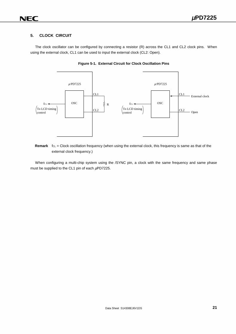
5. CLOCK CIRCUIT
The clock oscillator can be configured by connecting a resistor (R) across the CL1 and CL2 clock pins. Whenusing the external clock, CL1 can be used to input the external clock (CL2: Open).
Figure 5-1. External Circuit for Clock Oscillation Pins
OSC
CL1
R
CL2
fCL
To LCD timingcontrol
PD7225µ
OSC
CL1External clock
OpenCL2
fCL
To LCD timingcontrol
PD7225µ
Remark fCL = Clock oscillation frequency (when using the external clock, this frequency is same as that of theexternal clock frequency.)
When configuring a multi-chip system using the /SYNC pin, a clock with the same frequency and same phasemust be supplied to the CL1 pin of each µPD7225.

Data Sheet S14308EJ6V1DS22
µµµµPD7225
6. RESET FUNCTION
When a low level of 12 clock cycles or more is input to the /RESET pin, the µPD7225 will be reset to the followingconditions:
• This condition is the same as when M2 − M0 = 0, F1, F0 = 0 are executed by the MODE SET command.• Display data transfer from the data memory to the display data latch −−− This condition is the same as when
the UNSYNCHRONIZED TRANSFER command is executed.• Command/data register output −−− This condition is the same as when the WITHOUT SEGMENT DECODER
command is executed.• LCD display −−− This condition is the same as when the DISPLAY OFF or the BRINKING OFF command is
executed.
Function when the µPD7225 is reset
• S0-S31 and COM0-COM3 pins output VDD
• Serial data input −−− Disabled (/BUSY = 0) (However, /CS = 0)
When used in a multi-chip system, the reset state must be released (rising edge of /RESET) within 5 µs.
Figure 6-1. Reset Signal in Multi-Chip System
/RESET0.7VDD
0.3VDD
12 clock cycles 5 s max.µ

Data Sheet S14308EJ6V1DS 23
µµµµPD7225
7. SERIAL DATA INPUT
Serial data is input to the SI pin with MSB first in synchronization with the serial clock in 8-bits units. When /CS isset to low, the µPD7225 sets the /BUSY to low (this initializes the SCK counter and the data pointer to 0) in order toperform internal processing. Therefore, after the µPD7225 completes internal processing, the first bit (MSB) shouldbe input in synchronization with the /SCK after the /BUSY signal is set to high. The serial data is transferred to theserial register in bit units at the rising edge of /SCK. Inputting eight serial clocks completes the transfer of all 8 bits ofdata to the serial register. At the rising edge of the eighth serial clock, the /BUSY is set to low, and the status of theC, /D pin is clocked in to specify whether the data is a command or data. Afterwards, the contents of the serialregister are clocked into the command/data register.
When successively inputting 2 or more bytes of serial data, /CS must be set to low until all bytes of data are input.The /BUSY is set to low each time a byte of data is input. The /BUSY becomes high when the serial data is clockedin from the serial register to the command/data register, so that the next serial data can be input.
When input of all serial data is complete, the data memory contents can be displayed by setting /CS to high. /CSmust not be set to high while display data is being transferred (before eight clocks has elapsed.) If it becomesnecessary to interrupt serial data transfer when transferring two or more bytes of data due to an interrupt for the CPUinterrupt, execute the PAUSE TRANSFER command after checking that the byte has been transferred, then set /CSto high. In this case, even if /CS is set to high, the contents of the data memory will not be transferred to the displaydata latch.
To resume serial data transfer, set /CS to low in the same way as when initiating a normal transfer. However, inthis case, the contents of the data pointer are not cleared so that data write operation starts from the next datamemory address when serial data transfer is resumed (C, /D = 0).
Note In a multi-chip system in which the /BUSY pins of chips are made a wired-OR connection, avoid setting the/CS pins of two or more chips simultaneously.
Figure 7-1. Inputting Byte
Serial data(SI pin)
Highimpedance
D7 D6 D5 D0D1D2
Highimpedance
/SCK
/CS
/BUSY
C, /D
Figure 7-2. Inputting 5 Bytes Successively
Serial data Byte 2Byte 1 Byte 3 Byte 4 Byte 5
/CS
/BUSY

Data Sheet S14308EJ6V1DS24
µµµµPD7225
8. COMMAND
8.1 MODE SET
0 1 0 M2 M1 M0 F1 F0
This command sets the number of time divisions for the LCD display static drive or the time-division drive, biasmethod, and frame frequency.
(1) M1 and M0 specify the number of time divisions for static drive or time-division drive.
M1 M00 0 ------------------- Divide-by-4 time division drive1 0 ------------------- Divide-by-3 time division drive1 1 ------------------- Divide-by-2 time division drive0 1 ------------------- Static drive
(2) M2 specifies the bias method.
M20--------------------------- 1/3 bias method1--------------------------- 1/2 bias method
0/1 ------------------------- Static
(3) F1 and F0 specify the frequency division ratio which determines the frame frequency (refer to Figure 3-1).
F1 F0 Frequency division ratio0 0 ------------------- 1/27
0 1 ------------------- 1/28
1 0 ------------------- 1/29
1 1 ------------------- 1/211
8.2 SYNCHRONIZED TRANSFER
0 0 1 1 0 0 0 1
This command controls display data modification.Normally, modification of display data is performed at the rising edge of the /CS signal (transferring display data
from the data memory to the display data latch). However, after this command is executed, display data is modifiedat the first alternate current drive cycle (Frame frequency x Number of time divisions) after the /CS signal is set tohigh.

Data Sheet S14308EJ6V1DS 25
µµµµPD7225
8.3 UNSYNCHRONIZED TRANSFER
0 0 1 1 0 0 0 0
This command controls display data modification.After this command is executed, display data is modified at the rising edge of the /CS pin.
8.4 PAUSE TRANSFER
0 0 1 1 1 0 0 0
This command disables display data modification.After this command is executed, display data can not be modified at the first rising edge of the /CS pin; instead,
modification is put off until the second rising edge of the /CS pin. In addition, the data pointer is not cleared at thefirst rising edge of the /CS pin (refer to 2.5 Data Memory/Data Pointer).
This command is used when it becomes necessary to set the /CS pin to high due to an interrupt for the CPU in themiddle of serial data input operation.
8.5 BLINKING ON
0 0 0 1 1 0 1 K0
This command sets the blinking operation status. The blinking frequency is set by the least significant bit of thecommand (bit K0).
K0 Blinking frequency (Hz)
0 fCL/217
1 fCL/216
Remark fCL: Clock oscillation frequency
8.6 BLINKING OFF
0 0 0 1 1 0 0 0
This command stops blinking operation.
8.7 DISPLAY ON
0 0 0 1 0 0 0 1
After this command is executed, LCD display operation starts according to the display data contained in thedisplay data latch.

Data Sheet S14308EJ6V1DS26
µµµµPD7225
8.8 DISPLAY OFF
0 0 0 1 0 0 0 0
When this command is executed, the relationship of all common drive signals and segment drive signals entersthe non-select state. As a result, the display is turned off. Transferring display data from the data memory to thedisplay data latch is not affected by this command execution.
8.9 WITH SEGMENT DECODER
0 0 0 1 0 1 0 1
After this command is executed, input data is sent to the segment decoder, and the decoded code is written to thedata memory.
8.10 WITHOUT SEGMENT DECODER
0 0 0 1 0 1 0 0
After this command is executed, input data is written to the data memory without going through the segmentdecoder.
8.11 LOAD DATA POINTER
1 1 1 D4 D3 D2 D1 D0
This command sets immediate data D4-D0 to the data pointer.
8.12 WRITE DATA MEMORY
1 1 0 1 D3 D2 D1 D0
This command stores immediate data D3-D0 to the data memory addressed by the data pointer, and increments(+1) the contents of the data pointer.
8.13 OR DATA MEMORY
1 0 1 1 D3 D2 D1 D0
This command ORs the contents of the data memory addressed by the data pointer and immediate data D3-D0,and stores the result to the data memory, then increments (+1) the contents of the data pointer.

Data Sheet S14308EJ6V1DS 27
µµµµPD7225
8.14 AND DATA MEMORY
1 0 0 1 D3 D2 D1 D0
This command ANDs the contents of the data memory addressed by the data pointer and immediate data D3-D0,and stores the result to the data memory, then increments (+1) the contents of the data pointer.
8.15 CLEAR DATA MEMORY
0 0 1 0 0 0 0 0
This command clears the contents of the data memory and the data pointer.
8.16 WRITE BLINKING DATA MEMORY
1 1 0 0 D3 D2 D1 D0
This command stores immediate data D3-D0 to the blinking data memory addressed by the data pointer, andincrements (+1) the contents of the data pointer.
8.17 OR BLINKING DATA MEMORY
1 0 1 0 D3 D2 D1 D0
This command ORs the contents of the blinking data memory addressed by the data pointer and immediate dataD3-D0, and stores the result to the blinking data memory, then increments (+1) the contents of the data pointer.
8.18 AND BLINKING DATA MEMORY
1 0 0 0 D3 D2 D1 D0
This command ANDs the contents of the blinking data memory addressed by the data pointer and immediate dataD3-D0, and stores the result to the blinking data memory, then increments (+1) the contents of the data pointer.
8.19 CLEAR BLINKING DATA MEMORY
0 0 0 0 0 0 0 0
This command clears the contents of the blinking data memory and the data pointer.

Data Sheet S14308EJ6V1DS28
µµµµPD7225
9. DISPLAY OUTPUT
The following describes the serial data organization, display data organization in the data memory, segment drivesignal, and common drive signal when the display is active in the static and divide-by-2, -3, -4 time division modes.
9.1 Static
When displaying just the digit “6” in the static mode:
(1) Serial data organization: 0D, 07(2) Display data organization in the data memory
Address
n + 7 n + 6 n + 5 n + 4 n +3 n + 2 n + 1 n
Bit Contents of bit 0 0 1 1 1 1 1 0 1
(3) Power supply (static)VLC0 = VLC1 = VDD
VLC2 = VLC3 = VDD − VLCD
(4) Relationship between common and segment
SEGn + 1
SEGn
SEGn + 3
SEGn + 6
SEGn + 2
SEGn + 5
SEGn + 4
COM0
SEGn +7

Data Sheet S14308EJ6V1DS 29
µµµµPD7225
(5) Segment and common drive signals
VLC0
VLC3
SEGn, SEGn + 2 − SEGn + 6
VLC0
VLC3
SEGn + 1, SEGn + 7
VLC0
VLC3
COM0
VLC0
0
−VLC0
0
COM0 − SEGn
COM0 − SEGn + 1

Data Sheet S14308EJ6V1DS30
µµµµPD7225
9.2 Divide-by-2 Time Division
When displaying just the digit “6” in the divide-by-2 time division mode:
(1) Serial data organization: F5(2) Display data organization in the data memory
Address
n +3 n + 2 n + 1 n
Contents of bit 0 1 1 1 1
Contents of bit 1 1 1 0 0
(3) Power supply (1/2 bias)VLC0 = VDD
VLC1 = VLC2 = VDD − 1/2 VLCD
VLC3 = VDD − VLCD
(4) Relationship between common and segment
SEGn
COM0
COM1
SEGn + 3
SEGn + 2
SEGn + 1
Bit

Data Sheet S14308EJ6V1DS 31
µµµµPD7225
(5) Segment and common drive signals
VLC0
VLC3
SEGn + 3
VLC0
VLC3
SEGn + 2
VLC0
VLC3
SEGn + 1
VLC0
VLC3
SEGn
VLC0
VLC3
VLC1
VLC1
COM0
VLC0
VLC3
COM1
VLC0
0
0
−VLC0
VLC1
−VLC1
COM0 − SEGn + 3
VLC1
−VLC1
COM1 − SEGn
t0 t1 t2 t3 t0 t1 t2 t3 t0 t1

Data Sheet S14308EJ6V1DS32
µµµµPD7225
9.3 Divide-by-3 Time Division
When displaying the digit “6.” in the divide-by-3 time division mode:
(1) Serial data organization• Without segment decoder : FE• With segment decoder : 06
(However, the floating point is set to “1” by command.)(2) Display data organization in the data memory
Address
n + 2 n + 1 n
Contents of bit 0 1 1 0
Bit Contents of bit 1 1 1 1
Contents of bit 2 0 1 1
(3) Power supply (1/3 bias)VLC0 = VDD
VLC1 = VDD − 1/3 VLCD
VLC2 = VDD − 2/3 VLCD
VLC3 = VDD − VLCD
(4) Relationship between common and segment
SEGn + 1
COM2
SEGn
COM1
SEGn + 2
COM0

Data Sheet S14308EJ6V1DS 33
µµµµPD7225
(5) Segment and common drive signals
VLC0
VLC3
SEGn + 1
VLC0
VLC1
VLC2
VLC1
VLC2
VLC1
VLC2
VLC1
VLC2
VLC1
VLC2
VLC1
VLC2
VLC3
SEGn
VLC0
VLC3
SEGn + 2
VLC0
VLC3
COM0
VLC0
VLC3
COM1
VLC0
VLC0
COM2
VLC0
0
0
−VLC0
VLC2
−VLC2
COM1 − SEGn + 2
VLC2
−VLC2
COM2 − SEGn + 2
t0 t1 t2 t3 t4 t5 t0 t1 t2 t3

Data Sheet S14308EJ6V1DS34
µµµµPD7225
9.4 Divide-by-4 Time Division
When displaying the digit “6.” in the divide-by-4 time division mode:
(1) Serial data organization• Without segment decoder : FD• With segment decoder : 06
(However, the floating point is set to “1” by command.)
Address
n + 1 n
Contents of bit 0 1 1
Contents of bit 1 1 0
Contents of bit 2 1 1
Contents of bit 3 1 1
(2) Power supply (1/3 bias)VLC0 = VDD
VLC1 = VDD − 1/3 VLCD
VLC2 = VDD −2/3 VLCD
VLC3 = VDD − VLCD
(3) Relationship between common and segment
SEGn
SEGn + 1
COM1
COM3
COM0
COM2
Bit

Data Sheet S14308EJ6V1DS 35
µµµµPD7225
(4) Segment and common drive signals
VLC0
t7 t0 t1 t2 t7 t0 t1 t2t3 t4 t5 t6
VLC1
VLC2
VLC3
SEGn + 1
VLC0
VLC1
VLC2
VLC3
SEGn
VLC0
VLC1
VLC2
VLC3
COM0
VLC0
VLC1
VLC2
VLC3
COM3
VLC0
VLC1
VLC2
VLC3
COM1
VLC0
VLC1
VLC2
VLC3
COM2
VLC0
VLC2
0
−VLC2
−VLC0
COM0 − SEGn + 1
VLC2
0
−VLC2
COM1 − SEGn

Data Sheet S14308EJ6V1DS36
µµµµPD7225
10. ELECTRICAL CHARACTERISTICS
Absolute Maximum Rating (TA = 25 °°°°C)
Item Symbol Condition Rating Units
Power supply voltage VDD −0.3 to +7.0 V
Input voltage VI −0.3 to VDD +0.3 V
Output voltage VO −0.3 to VDD +0.3 V
Operating ambient temperature TA −10 to +70 °C
Storage temperature Tstg −65 to +150 °C
Caution If the absolute maximum rating of even one of the above parameters is exceededeven momentarily, the quality of the product may be degraded. Absolute maximumratings, therefore, specify the values exceeding which the product may be physicallydamaged. Be sure to use the product within the range of the absolute maximumratings.
Capacitance (TA = 25 °°°°C, VDD = 0 V)
Item Symbol Condition MIN. TYP. MAX. Units
Input capacitance CIN 10 pF
Output capacitance COUT1 Except /BUSY 20 pF
Output capacitance COUT2 /BUSY 15 pF
Input/output capacitance CIO /SYNC 15 pF
Clock capacitance CC CL1 30 pF
f = 1 MHz pinsother than thoseused formeasurement
are 0 V.

Data Sheet S14308EJ6V1DS 37
µµµµPD7225
DC Characteristics (TA = −−−−10 to +70 °°°°C, VDD = 5 V ±±±± 10%)
Item Symbol Condition MIN. TYP. MAX. Unit
High level input voltage VIH 0.7 VDD VDD V
Low level input voltage VIL 0 0.3 VDD V
High level output voltage VOH /SYNC, /BUSY, IOH = −10 µA VDD − 0.5 V
Low level output voltage VOL1 /BUSY, IOL = 100 µA 0.5 V
VOL2 /SYNC, IOL = 900 µA 1.0 V
Output short-circuit current IOS /SYNC, VO = 1 V −300 µA
High level input leakage current ILIH VI = VDD 2 µA
Low level input leakage current ILIL VI = 0 V −2 µA
High level output leakage current ILOH VO = VDD 2 µA
Low level output leakage current ILOL VO = 0 V −2 µA
Common output impedance RCOM COM0 to COM3Note 1, VDD ≥ VLCD 5 7 kΩ
Segment output impedance RSEG S0 to S31Note 1, VDD ≥ VLCD 7 14 kΩ
Power supply voltage IDD CL1 external clock, fC = 200 kHzNote 2 100 250 µA
Notes 1. Applies to Static, 1/2 bias, 1/3 bias2. Abnormal current will flow if the external clock supply is removed.
DC Characteristics (TA = 0 to +70 °°°°C, VDD = 2.7 to 5.5 V)
Item Symbol Condition MIN. TYP. MAX. Units
High level input voltage VIH1 Except /SCK 0.7 VDD VDD V
VIH2 /SCK 0.8 VDD VDD V
Low level input voltage VIL1 Except /SCK 0 0.3 VDD V
VIL2 /SCK 0 0.2 VDD V
High level output voltage VOH /SYNC, /BUSY, IOH = −7 µA VDD − 0.75 V
Low level output voltage VOL1 /BUSY, IOL = 100 µA 0.5 V
VOL2 /SYNC, IOL = 400 µA 0.5 V
Output short-circuit current IOS /SYNC, VO = 0.5 V −200 µA
High level input leakage current ILIH VI = VDD 2 µA
Low level input leakage current ILIL VI = 0 V −2 µA
High level output leakage current ILOH VO = VDD 2 µA
Low level output leakage current ILOL VO = 0 V −2 µA
Common output impedance RCOM COM0 to COM3Note 1, VDD ≥ VLCD 6 kΩ
Segment output impedance RSEG S0 to S31Note 1, VDD ≥ VLCD 12 kΩ
Power supply voltage IDD CL external clock, VDD = 3 V ± 10%,fC = 140 kHzNote 2
30 100 µA
Notes 1. Applies to Static and 1/3 bias2. Abnormal current will flow if the external clock supply is removed.
Data Sheet S14308EJ6V1DS38
µµµµPD7225
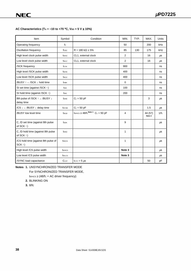
AC Characteristics (TA = −−−−10 to +70 °°°°C, VDD = 5 V ±±±± 10%)
Item Symbol Condition MIN. TYP. MAX. Units
Operating frequency fC 50 200 kHz
Oscillation frequency fOSC R = 180 kΩ ± 5% 85 130 175 kHz
High level clock pulse width tWHC CL1, external clock 2 16 µs
Low level clock pulse width tWLC CL1, external clock 2 16 µs
/SCK frequency tCYK 900 ns
High level /SCK pulse width tWHK 400 ns
Low level /SCK pulse width tWLK 400 ns
/BUSY ↑→ /SCK ↓ hold time tHBK 0 ns
SI set time (against /SCK ↑) tSIK 100 ns
SI hold time (against /SCK ↑) tHKI 200 ns
8th pulse of /SCK ↑→ /BUSY ↓delay time
tDKB CL = 50 pF 3 µs
/CS ↓→ /BUSY ↓ delay time tDCSB CL = 50 pF 1.5 µs
/BUSY low level time tWLB tWHCS ≥ 48/fCNote 1 CL = 50 pF 4 44 (57)Note 2
1/fC
C, /D set time (against 8th pulseof SCK ↑)
tSDK 9 µs
C, /D hold time (against 8th pulseof SCK ↑)
tHKD 1 µs
/CS hold time (against 8th pulse ofSCK ↑)
tHKCS 1 µs
High level /CS pulse width tWHCS Note 3 µs
Low level /CS pulse width tWLCS Note 3 µs
/SYNC load capacitance CLSY tCYC = 5 µs 50 pF
Notes 1. UNSYNCHRONIZED TRANSFER MODEFor SYNCHRONIZED TRANSFER MODE,tWHCS ≥ (48/fC + AC driver frequency)
2. BLINKING ON3. 8/fc

Data Sheet S14308EJ6V1DS 39
µµµµPD7225
AC Characteristics (TA = 0 to +70 °°°°C, VDD = 2.7 V to 5.5 V)
Item Symbol Condition MIN. TYP. MAX. Unit
Operating frequency fC 50 140 kHz
Oscillation frequency fOSC R = 180 kΩ ± 5%, VDD = 3 V ± 10 % 50 100 140 kHz
High level clock pulse width tWHC CL1, external clock 3 16 µs
Low level clock pulse width tWLC CL1, external clock 3 16 µs
/SCK frequency tCYK 4 µs
High level /SCK pulse width tWHK 1.8 µs
Low level /SCK pulse width tWLK 1.8 µs
/BUSY ↑→ /SCK hold time tHBK 0 ns
SI set time (against /SCK ↑) tSIK 1 µs
SI hold time (against /SCK ↑) tHKI 1 µs
8th pulse of /SCK ↑→ /BUSY ↓delay time
tDKB CL = 50 pF 5 µs
/CS ↓→ /BUSY ↓ delay time tDCSB CL = 50 pF 5 µs
/BUSY low level time tWLB tWHCS ≥ 48/fCNote 1 CL = 50 pF 4 44 (57)Note 2
1/fC
C, /D set time (against 8th pulseof SCK ↑)
tSDK 18 µs
C, /D hold time (against 8th pulseof SCK ↑)
tHKD 1 µs
/CS hold time (against 8th pulse ofSCK ↑)
tHKCS 1 µs
High level /CS pulse width tWHCS Note 3 µs
Low level /CS pulse width tWLCS Note 3 µs
/SYNC load capacitance CLSY tCYC = 7.1 µs 50 pF
Notes 1. UNSYNCHRONIZED TRANSFER MODFor SYNCHRONIZED TRANSFER MODE,tWHCS ≥ (48/fC + AC driver frequency)
2. BLINKING ON3. 8/fc
AC Timing Measurement Voltage
Measurementpoints
0.7VDD
0.3VDD
0.7VDD
0.3VDD

Data Sheet S14308EJ6V1DS40
µµµµPD7225
Timing Wave-Form
CL1
/CS
/BUSY
/SCK
SI
C, /D
tCYC (1/fe)
tWHC
tWLC
tWLCS
tHBK
0.5 V 0.5 VtCYK
tWLK
tWHK
tSIK tHKI
tSDK tHKD
tDKB tWLR
tDCSB
Note 1
Note 2
Note 3
tWHCS
tHKCS
Notes 1. VDD − 0.5 V when VDD = 5 V ± 10 %, VDD − 0.75 V when VDD = 2.7 to 5.5 V2. 0.8 V when VDD = 2.7 V to 5.5 V3. 0.2 V when VDD = 2.7 V to 5.5 V

Data Sheet S14308EJ6V1DS 41
µµµµPD7225
Typical Characteristic Curve (Ta = 25 °°°°C)
External resistor and oscillation frequency
External resistor R (k ohms)
Osc
illat
ion
freq
uenc
y (k
Hz)
200
50
100
200
500100
CL2 CL1
R
Power supply voltage and operating current
Power supply voltage VDD (V)
Ope
ratin
g cu
rren
t (
A)
4
20
50
100
5 63
CL2 CL1
External clock
Power supply voltage and oscillation frequency
Power supply voltage VDD (V)O
scill
atio
n fr
eque
ncy
(kH
z)
4 5
80
100
120
140
63
CL2 CL1
R
fC = 200 kHz
fC = 140 kHz
VDD = 3 V
VDD = 5 V
R = 180 kΩ
µ
Data Sheet S14308EJ6V1DS42
µµµµPD7225
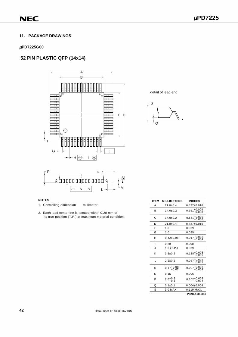
11. PACKAGE DRAWINGS
µµµµPD7225G00
M
S
52 PIN PLASTIC QFP (14x14)
NOTES
1. Controlling dimension millimeter.
2. Each lead centerline is located within 0.20 mm of its true position (T.P.) at maximum material condition.
I
ITEM MILLIMETERS INCHES
B 14.0±0.2 0.551
D 21.0±0.4 0.827±0.016
F 1.0 0.039
A 21.0±0.4 0.827±0.016
H 0.42±0.08 0.017
I 0.20 0.008
Q 0.1±0.1 0.004±0.004
S 3.0 MAX. 0.119 MAX.
P52G-100-00-3
+0.009−0.008
+0.003−0.004
G 1.0 0.039
J 1.0 (T.P.) 0.039
K 3.5±0.2 0.138+0.008−0.009
L 2.2±0.2 0.087+0.008−0.009
detail of lead end
Q
K
L
P
H
G
F
S
J
N
C 14.0±0.2 0.551+0.009−0.008
M 0.17 0.007+0.003−0.004
+0.08−0.07
N 0.15 0.006
P 2.6 0.102+0.009−0.004
+0.2−0.1
3940 26
27
152 14
13
S
A
B
C D
M

Data Sheet S14308EJ6V1DS 43
µµµµPD7225
µµµµPD7225G01
52-PIN PLASTIC QFP (STRAIGHT) (14x14)
ITEM MILLIMETERS
A
B
D
G
H
22.0±0.4
14.0±0.2
1.0 (T.P.)
0.40±0.10
1.0
J
22.0±0.4
K
P52G-100-01-3
C 14.0±0.2
I 0.20
4.0±0.2
F 1.0
T
U
1.0
1.45
M 0.15+0.10−0.05
P 2.6+0.2−0.1
NOTE
Each lead centerline is located within 0.20 mm ofits true position (T.P.) at maximum material condition.
3940
521 1413
2726
J
C D
A
B
K
M
P
U
T
I
G
F
MH

Data Sheet S14308EJ6V1DS44
µµµµPD7225
µµµµPD7225GB-3B7
56-PIN PLASTIC QFP (10x10)
ITEM MILLIMETERS
A
B
D
G
H
13.2±0.4
10.0±0.2
0.65 (T.P.)
0.30±0.10
0.75
J
13.2±0.4
K
S56GB-65-3B7-4
C 10.0±0.2
I 0.13
1.6±0.2L 0.8±0.2
F 0.75
N
P
Q
S
0.10
2.7
0.1±0.1
3.0 MAX.
R 5°±5°
M 0.15+0.10−0.05
NOTE
Each lead centerline is located within 0.13 mm ofits true position (T.P.) at maximum material condition.
4243 28
561
1514
29
S
SN
J
detail of lead end
C D
A
B
R
K
M
L
P
I
S
Q
G
F
MH
Data Sheet S14308EJ6V1DS 45
µµµµPD7225
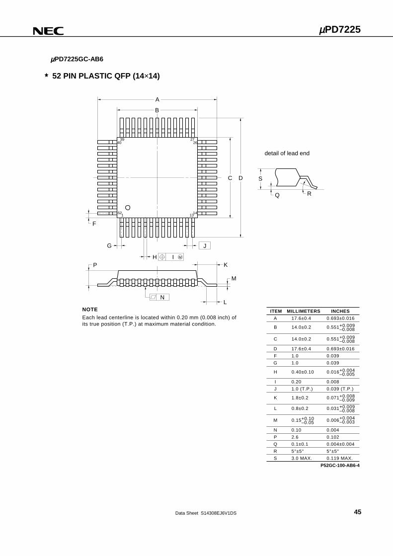
µµµµPD7225GC-AB6
52 PIN PLASTIC QFP (14×14)
ITEM MILLIMETERS INCHESNOTE
Each lead centerline is located within 0.20 mm (0.008 inch) ofits true position (T.P.) at maximum material condition.
P52GC-100-AB6-4
L 0.8±0.2 0.031+0.009–0.008
M 0.15 0.006
N 0.10 0.004
P 2.6 0.102
A 17.6±0.4 0.693±0.016
B 14.0±0.2 0.551+0.009–0.008
C 14.0±0.2 0.551+0.009–0.008
D 17.6±0.4 0.693±0.016
F 1.0 0.039
G 1.0 0.039
H 0.40±0.10 0.016+0.004–0.005
I 0.20 0.008
J 1.0 (T.P.) 0.039 (T.P.)
K 1.8±0.2 0.071+0.008–0.009
Q 0.1±0.1 0.004±0.004
+0.10–0.05
+0.004–0.003
M
M
K
J
H
Q
P
N
R
detail of lead end
I
G
R 5°±5° 5°±5°S 3.0 MAX. 0.119 MAX.
3940
521
2627
1413
A
B
C D
L
F
S

Data Sheet S14308EJ6V1DS46
µµµµPD7225
12. RECOMMENDED SOLDERING CONDITIONS
When mounting the µPD7225 by soldering, soldering should be performed under the following recommendedconditions.
Should other than recommended conditions be used, consult with our sales personnel.
Surface Mount Type
µPD7225G00 : 52-pin plastic QFP (14 × 14 mm)µPD7225G01 : 52-pin plastic QFP (straight) ( 14 × 14 mm)µPD7225GC-AB6 : 52-pin plastic QFP (14 × 14 mm)
Soldering Method Soldering ConditionSymbol of
RecommendedSoldering Condition
Partial heating Pin temperature: 300 °C MAX., Time: 3 seconds MAX. (per pin row) −
µPD7225GB-3B7 : 56-pin plastic QFP (10 × 10 mm)
Soldering Method Soldering ConditionSymbol of
RecommendedSoldering Condition
Infrared reflow Package peak temperature: 235 °C, Time: 30 seconds MAX. (210 °C or higher),Count: 3 times or less
IR35-00-3
VPS Package peak temperature: 215 °C, Time: 40 seconds MAX. (200 °C or higher),Count: 3 times or less
VP-15-00-3
Wave soldering Solder bath temperature: 260 °C MAX., Time: 10 seconds MAX., Counts: 1,Preheating temperature: 120 °C MAX. (package surface temperature)
WS-60-00-1
Partial heating Pin temperature: 300 °C MAX., Time: 3 seconds MAX. (per pin row) −
Caution Do not use two or more soldering methods in combination (except the partial heating method).
Reference DocumentsNEC Semiconductor Device Reliability / Quality Control System (C10983E)Quality Grades to NEC’s Semiconductor Devices (C11531E)Semiconductor Device Mounting Technology Manual (C10535E)

Data Sheet S14308EJ6V1DS 47
µµµµPD7225
NOTES FOR CMOS DEVICES
1 PRECAUTION AGAINST ESD FOR SEMICONDUCTORS
Note:
Strong electric field, when exposed to a MOS device, can cause destruction of the gate oxide and
ultimately degrade the device operation. Steps must be taken to stop generation of static electricity
as much as possible, and quickly dissipate it once, when it has occurred. Environmental control
must be adequate. When it is dry, humidifier should be used. It is recommended to avoid using
insulators that easily build static electricity. Semiconductor devices must be stored and transported
in an anti-static container, static shielding bag or conductive material. All test and measurement
tools including work bench and floor should be grounded. The operator should be grounded using
wrist strap. Semiconductor devices must not be touched with bare hands. Similar precautions need
to be taken for PW boards with semiconductor devices on it.
2 HANDLING OF UNUSED INPUT PINS FOR CMOS
Note:
No connection for CMOS device inputs can be cause of malfunction. If no connection is provided
to the input pins, it is possible that an internal input level may be generated due to noise, etc., hence
causing malfunction. CMOS devices behave differently than Bipolar or NMOS devices. Input levels
of CMOS devices must be fixed high or low by using a pull-up or pull-down circuitry. Each unused
pin should be connected to VDD or GND with a resistor, if it is considered to have a possibility of
being an output pin. All handling related to the unused pins must be judged device by device and
related specifications governing the devices.
3 STATUS BEFORE INITIALIZATION OF MOS DEVICES
Note:
Power-on does not necessarily define initial status of MOS device. Production process of MOS
does not define the initial operation status of the device. Immediately after the power source is
turned ON, the devices with reset function have not yet been initialized. Hence, power-on does
not guarantee out-pin levels, I/O settings or contents of registers. Device is not initialized until the
reset signal is received. Reset operation must be executed immediately after power-on for devices
having reset function.

µµµµPD7225
M8E 00. 4
The information in this document is current as of May, 2002. The information is subject to change without notice. For actual design-in, refer to the latest publications of NEC's data sheets or data books, etc., for the most up-to-date specifications of NEC semiconductor products. Not all products and/or types are available in every country. Please check with an NEC sales representative for availability and additional information.No part of this document may be copied or reproduced in any form or by any means without prior written consent of NEC. NEC assumes no responsibility for any errors that may appear in this document.NEC does not assume any liability for infringement of patents, copyrights or other intellectual property rights of third parties by or arising from the use of NEC semiconductor products listed in this document or any other liability arising from the use of such products. No license, express, implied or otherwise, is granted under any patents, copyrights or other intellectual property rights of NEC or others.Descriptions of circuits, software and other related information in this document are provided for illustrative purposes in semiconductor product operation and application examples. The incorporation of these circuits, software and information in the design of customer's equipment shall be done under the full responsibility of customer. NEC assumes no responsibility for any losses incurred by customers or third parties arising from the use of these circuits, software and information.While NEC endeavours to enhance the quality, reliability and safety of NEC semiconductor products, customers agree and acknowledge that the possibility of defects thereof cannot be eliminated entirely. To minimize risks of damage to property or injury (including death) to persons arising from defects in NEC semiconductor products, customers must incorporate sufficient safety measures in their design, such as redundancy, fire-containment, and anti-failure features.NEC semiconductor products are classified into the following three quality grades:"Standard", "Special" and "Specific". The "Specific" quality grade applies only to semiconductor products developed based on a customer-designated "quality assurance program" for a specific application. The recommended applications of a semiconductor product depend on its quality grade, as indicated below. Customers must check the quality grade of each semiconductor product before using it in a particular application. "Standard": Computers, office equipment, communications equipment, test and measurement equipment, audio
and visual equipment, home electronic appliances, machine tools, personal electronic equipmentand industrial robots
"Special": Transportation equipment (automobiles, trains, ships, etc.), traffic control systems, anti-disastersystems, anti-crime systems, safety equipment and medical equipment (not specifically designedfor life support)
"Specific": Aircraft, aerospace equipment, submersible repeaters, nuclear reactor control systems, lifesupport systems and medical equipment for life support, etc.
The quality grade of NEC semiconductor products is "Standard" unless otherwise expressly specified in NEC's data sheets or data books, etc. If customers wish to use NEC semiconductor products in applications not intended by NEC, they must contact an NEC sales representative in advance to determine NEC's willingness to support a given application.(Note)(1) "NEC" as used in this statement means NEC Corporation and also includes its majority-owned subsidiaries.(2) "NEC semiconductor products" means any semiconductor product developed or manufactured by or for
NEC (as defined above).
•
•
•
•
•
•