
Prof. V.G. OklobdzijaAdvanced Digital Integrated Circuits1 VLSI Prof. Vojin G. Oklobdzija References...
35
Prof. V.G. Oklobdzija Advanced Digital Integrated Circuits 1 VLSI Prof. Vojin G. Oklobdzija References (used for creation of the presentation material): [1] Mead, Conway, “Introduction to VLSI Systems”, Addison Wesley Publishing. [2] Glasser, Dobberpuhl, “The Design and Analysis of VLSI Circuits”, Addison Wesley Publishing. [3] Weste, Eshraghian, “Principles of CMOS VLSI Design”, Addison Wesley Publishing. [4] Shoji, “CMOS Digital Circuits Technology” , Prentice Hall.
-
Upload
virginia-tench -
Category
Documents
-
view
216 -
download
0
Transcript of Prof. V.G. OklobdzijaAdvanced Digital Integrated Circuits1 VLSI Prof. Vojin G. Oklobdzija References...
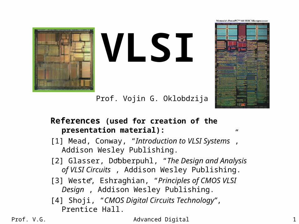
Prof. V.G. Oklobdzija Advanced Digital Integrated Circuits 1
VLSIProf. Vojin G. Oklobdzija
References (used for creation of the presentation material):
[1] Mead, Conway, “Introduction to VLSI Systems”, Addison Wesley Publishing.
[2] Glasser, Dobberpuhl, “The Design and Analysis of VLSI Circuits”, Addison Wesley Publishing.
[3] Weste, Eshraghian, “Principles of CMOS VLSI Design”, Addison Wesley Publishing.
[4] Shoji, “CMOS Digital Circuits Technology”, Prentice Hall.

Prof. V.G. Oklobdzija Advanced Digital Integrated Circuits 2
Historical Overview
• nMOS era: 1970-85• Pass-transistor design• Domino CMOS, 1982
– NORA– DCVSL
• CPL, DPL– DCVS-PG– SRPL– LEAP
• SOI-CMOS

Prof. V.G. Oklobdzija Advanced Digital Integrated Circuits 3
n-MOS Design Era
LSI started with nMOS:• pass-transistor design experience:
- Flourished at the beginning of the nMOS era
(popularized by Mead-Conway book)
- Allows high density layout and compact design style
- Fast: outperforming gate based design
- Low in power
• Drawbacks:– Not compatible with existing design tools
– Exhibiting testability and reliability problems

Prof. V.G. Oklobdzija Advanced Digital Integrated Circuits 4
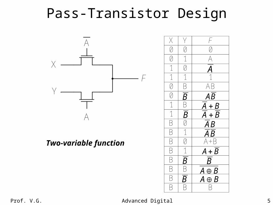
Pass-Transistor Design
Another way of looking at Karnaugh Map: AND function
0 10
1
0 1
B
A
1 0
A
A
B
B
F
F
B B
Prof. V.G. Oklobdzija Advanced Digital Integrated Circuits 5
Pass-Transistor Design
Two-variable function
A
A
X
Y
F
X Y F0 0 00 1 A1 01 1 10 B AB01 B1B 0B 1B 0 A+BB 1BB BBB B B
B
B
B
B
B
A
BA
BABA
BABA
BA
BA
BA

Prof. V.G. Oklobdzija Advanced Digital Integrated Circuits 6
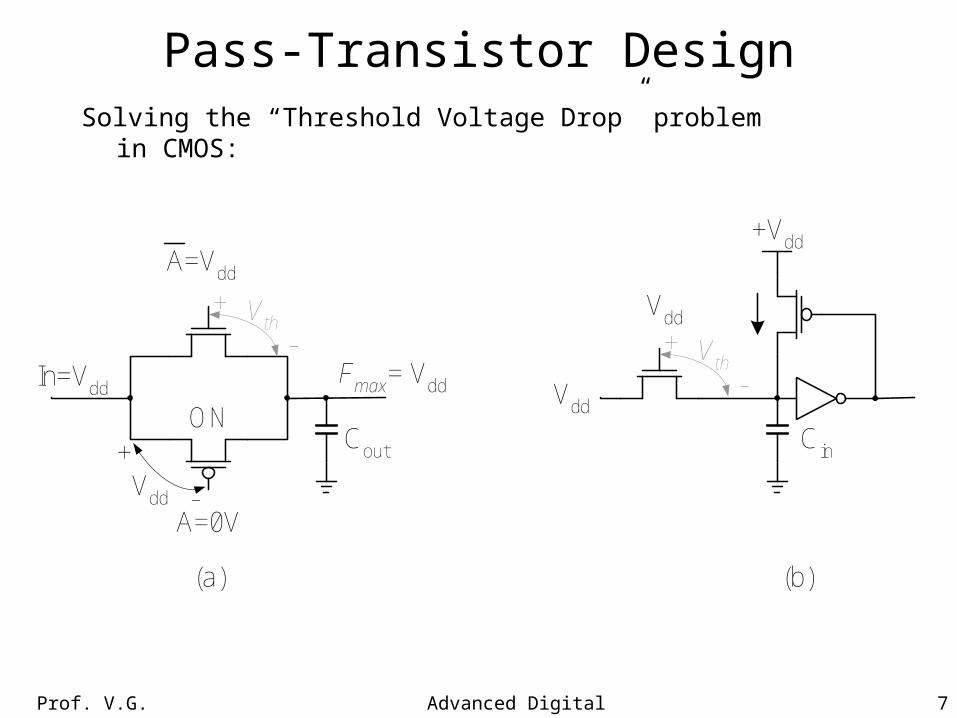
Pass-Transistor Design“Threshold Voltage Drop” problem:
A
B=Vdd
B
Fmax = Vdd-Vth
A=Vdd
Vth+
-
Cout
Vdd
Vdd
Fmax = Vdd-Vth
Cout
Vth+
-Vth
+
-
Vdd
(a) (b)
Prof. V.G. Oklobdzija Advanced Digital Integrated Circuits 7
Pass-Transistor DesignSolving the “Threshold Voltage Drop” problem in CMOS:
A=0V
In=VddFmax= Vdd
A=Vdd
Vth+
-
Cout
Vdd
Vdd
Cin
Vth+
-
(a) (b)
+
-Vdd
ON
+Vdd

Prof. V.G. Oklobdzija Advanced Digital Integrated Circuits 8
Pass-Transistor Design
Function Generator
A A B B
P0
P1
P2
P3
F(A,B)

Prof. V.G. Oklobdzija Advanced Digital Integrated Circuits 9
Pass-Transistor Design
Full 1-bit Adder A
A
A
S
A
A
S
OC
OC
B B C C
Prof. V.G. Oklobdzija Advanced Digital Integrated Circuits 10
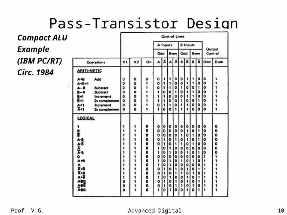
Pass-Transistor DesignCompact ALU
Example
(IBM PC/RT)
Circ. 1984
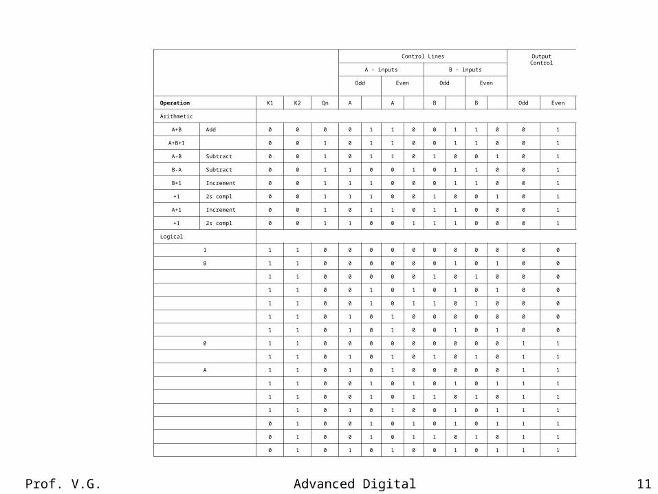
Prof. V.G. Oklobdzija Advanced Digital Integrated Circuits 11
Control Lines OutputControl
A - inputs B - inputs
Odd Even Odd Even
Operation K1 K2 Qn A A B B Odd Even
Arithmetic
A+B Add 0 0 0 0 1 1 0 0 1 1 0 0 1
A+B+1 0 0 1 0 1 1 0 0 1 1 0 0 1
A-B Subtract 0 0 1 0 1 1 0 1 0 0 1 0 1
B-A Subtract 0 0 1 1 0 0 1 0 1 1 0 0 1
B+1 Increment 0 0 1 1 1 0 0 0 1 1 0 0 1
+1 2s compl 0 0 1 1 1 0 0 1 0 0 1 0 1
A+1 Increment 0 0 1 0 1 1 0 1 1 0 0 0 1
+1 2s compl 0 0 1 1 0 0 1 1 1 0 0 0 1
Logical
1 1 1 0 0 0 0 0 0 0 0 0 0 0
B 1 1 0 0 0 0 0 0 1 0 1 0 0
1 1 0 0 0 0 0 1 0 1 0 0 0
1 1 0 0 1 0 1 0 1 0 1 0 0
1 1 0 0 1 0 1 1 0 1 0 0 0
1 1 0 1 0 1 0 0 0 0 0 0 0
1 1 0 1 0 1 0 0 1 0 1 0 0
0 1 1 0 0 0 0 0 0 0 0 0 1 1
1 1 0 1 0 1 0 1 0 1 0 1 1
A 1 1 0 1 0 1 0 0 0 0 0 1 1
1 1 0 0 1 0 1 0 1 0 1 1 1
1 1 0 0 1 0 1 1 0 1 0 1 1
1 1 0 1 0 1 0 0 1 0 1 1 1
0 1 0 0 1 0 1 0 1 0 1 1 1
0 1 0 0 1 0 1 1 0 1 0 1 1
0 1 0 1 0 1 0 0 1 0 1 1 1

Prof. V.G. Oklobdzija Advanced Digital Integrated Circuits 12
Pass-Transistor Design
Compact ALU
Example
(IBM PC/RT)
A B
K2 A
B
K1
A B K2
IC
OC
OCK2
A
B
f
HV
HV
Carry Generator
Function Generator
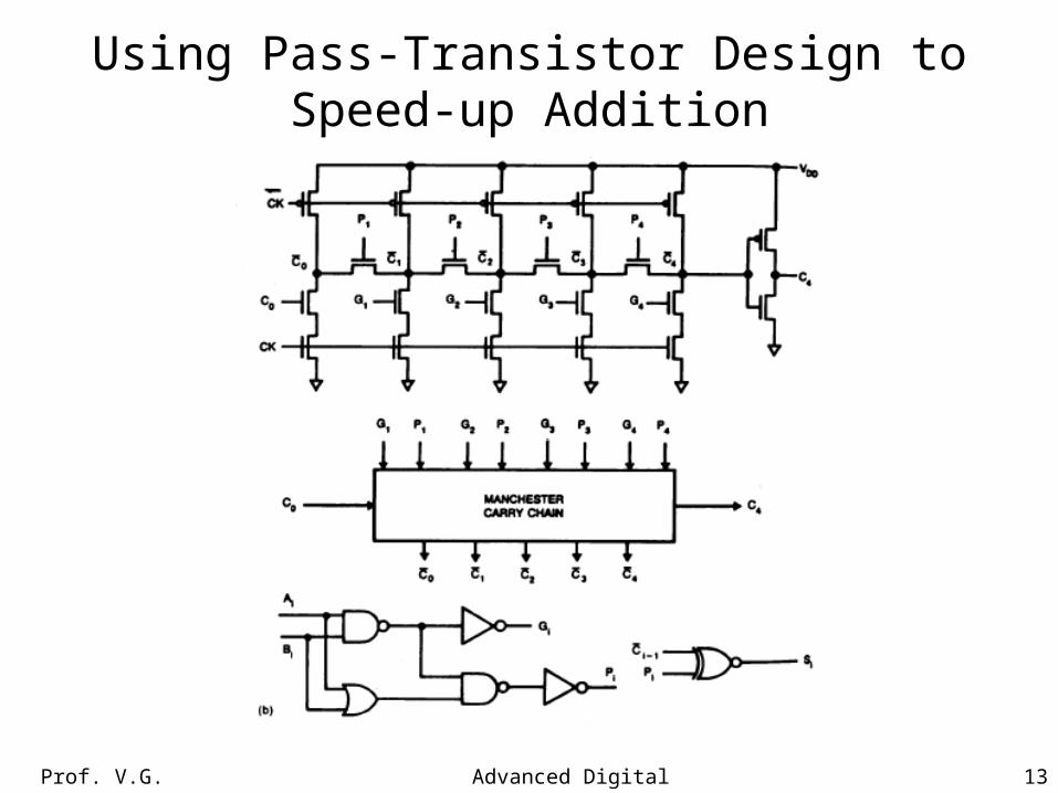
Prof. V.G. Oklobdzija Advanced Digital Integrated Circuits 13
Using Pass-Transistor Design to Speed-up Addition
Prof. V.G. Oklobdzija Advanced Digital Integrated Circuits 14
Review of CMOS
Prof. Vojin G. Oklobdzija
Prof. V.G. Oklobdzija Advanced Digital Integrated Circuits 15
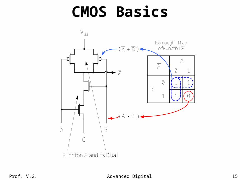
CMOS Basics
A B
C
Vdd
0
1B
A
10
1 1
1 0
)( A B+
( )BA
Function F and its Dual
Karnaugh Mapof Function F
FF

Prof. V.G. Oklobdzija Advanced Digital Integrated Circuits 16
CMOS Basics
Prof. V.G. Oklobdzija Advanced Digital Integrated Circuits 17
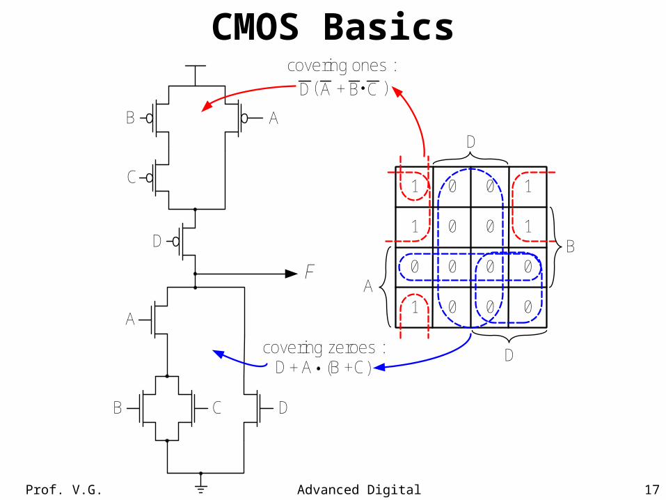
CMOS Basics
B A
C
D
A
B C D
1
1 0 0 0
0000
1001
100
( )BA +C+Dcovering zeroes :
( )+D A CB
covering ones :
A
B
D
D
F

Prof. V.G. Oklobdzija Advanced Digital Integrated Circuits 18
CMOS BasicsA complex path example:
VDD
A B
C DE
A
B
C
DE
Output

Prof. V.G. Oklobdzija Advanced Digital Integrated Circuits 19
CMOS BasicsMore complex blocks are realizable in CMOSPrimitive gates:

Prof. V.G. Oklobdzija Advanced Digital Integrated Circuits 20
CMOS Deficiencies: Muli-Input NOR function in CMOS is slow
Various remedies:

Prof. V.G. Oklobdzija Advanced Digital Integrated Circuits 21
CMOS Deficiencies and Remedies
A
B
B
A B + BA
A
BA B + BA
XOR Faster, one-levelrealizations of XOR
function
(a) (b)
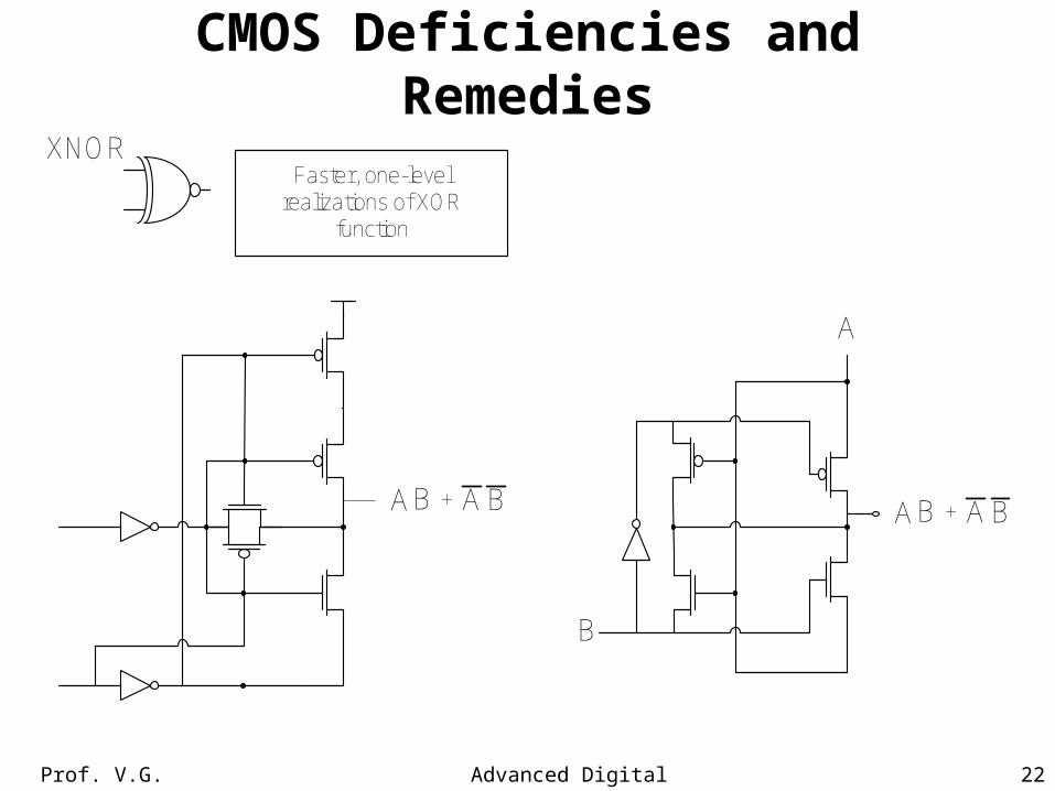
Prof. V.G. Oklobdzija Advanced Digital Integrated Circuits 22
CMOS Deficiencies and Remedies
AB + BA
A
B
XNOR
AB + BA
Faster, one-levelrealizations of XOR
function

Prof. V.G. Oklobdzija Advanced Digital Integrated Circuits 23
CMOS Basic
Inverter Transfer function:
Logic voltage levels are VOH and VOL
and VIL and VIH
The inverter transfer function lie
within the shaded region
VDD
VOH
VIH
Vout
VIL
VOL
0VOL VIL
Vin
VIH VOH VDD

Prof. V.G. Oklobdzija Advanced Digital Integrated Circuits 24
CMOS Basic: Inverter Characteristicp “ON”n “OFF’’
p ”OFF”n ”ON”
VDD
VDD
0.5VDD
0
0 0.5VDD VDD + VtpVtn
AB
C
DE
BOTH p & n “ON”

Prof. V.G. Oklobdzija Advanced Digital Integrated Circuits 25
CMOS Basic: Inverter Characteristic
+ VDD
t
t
0
+ VDD
0.9 VDD
0.1 VDD
VDD
Vin(t) 1T
2TV0(t)
LC
VDD
t
dt
ftrt

Prof. V.G. Oklobdzija Advanced Digital Integrated Circuits 26
CMOS Basic: Inverter CharacteristicTransistors during the transition

Prof. V.G. Oklobdzija Advanced Digital Integrated Circuits 27
CMOS Basic: Inverter Switching
CL
t = 0
VDDp-DEVICE
n-DEVICE
SATURATION :
VO
Ic
CL
VDDp-DEVICE
n-DEVICE
LINEAR :
VO
Ic
CL
t = 0
VDDp-DEVICE
n-DEVICE
SATURATION
VO
Ic
p-DEVICE
n-DEVICE
LINEAR
Rc
CL
VDD
VO
Ic
Rc
inDDO VVV inDDO VVV 0

Prof. V.G. Oklobdzija Advanced Digital Integrated Circuits 28
CMOS Basic: Power
• During the static state there is no current
• Current is only present during transistion:
- Short circuit current (crow-bar current)
- Charging and discharging of the output capacitor
- Leakage Current
t
t
t
VDD
VDD
VDD
0
0
0
V
V
I
tp
tftr

Prof. V.G. Oklobdzija Advanced Digital Integrated Circuits 29
CMOS Basic: Power
This is an E=mc2 of low-power designThere are three ways to control power:- Reducing Power-Supply Voltage (most effective !!)
- Reducing the switching activity k (various ways)
- Reducing CL (technology scaling etc.)
- Reducing the required frequency of operation (?)
PCMOS=kCLV2DDfo

Prof. V.G. Oklobdzija Advanced Digital Integrated Circuits 30
CMOS Basic: Delay • Which one of the three designs is the fastest ?
• How can we find this out without simulation ?
CL
Case 1
0a
7a
(a)
CL
Case 27a
4a
3a
0a
(b)
CL
Case 3
0a1a
3a2a
5a6a
4a
7a
(c)
Learn about Logical Effort !

Prof. V.G. Oklobdzija Advanced Digital Integrated Circuits 31
CMOS Basic: Delay
Cin1 Cin2Cout
DischargeId
Charge:Ic
DischargeId

Prof. V.G. Oklobdzija Advanced Digital Integrated Circuits 32
CMOS Basic: Delay
Delay can be approximated with:
RND7Cin1+RNORCin2+RND2Cout
CoutCin1 Cin2
Id Id
Ic
RND7
RNOR
RND2

Prof. V.G. Oklobdzija Advanced Digital Integrated Circuits 33
CMOS Basic: DelayDelay of a signal path in CMOS logic is dependent
on:• Fan-in of a gate
– Represented as a resistance of the pull-up/down transistor path of the gate
• Fan-out of a gate– Represented as a capacitive load at the output
• Number of CMOS blocks in the path.• Wire delay connecting various blocks.

Prof. V.G. Oklobdzija Advanced Digital Integrated Circuits 34
CMOS Basic: Delay
Delay of a signal path in CMOS logic can be reduced by:
• Making the transistors larger in order to minimize resistance of a pull-up/down path in the gate
• Making the transistors smaller in order to minimize the capacitive load of each gate
• Reducing the number of CMOS blocks in the path.• Bringing the blocks closer and/or choosing the
less wire intensive topology.– Note that these requirements are often contradictory

Prof. V.G. Oklobdzija Advanced Digital Integrated Circuits 35
CMOS Basic: Delay
• How to estimate delay and critical timing in CMOS circuits ?
• How to determine the proper transistor sizing in order to make a compromise with contradicting requirements ?
• How to choose the right circuit topology ?
The Answer:
“Logical Effort”


![VLSIVLSI Prof. Vojin G. Oklobdzija References (used for creation of the presentation material): [1] Mead, Conway, “Introduction to VLSI Systems”, Addison.](https://static.fdocuments.us/doc/165x107/56649ca65503460f94968ef2/vlsivlsi-prof-vojin-g-oklobdzija-references-used-for-creation-of-the-presentation.jpg)


