PRODUCT/PROCESS - mouser.com · change Qualification Plan results availability 19-Mar-2014 ... c2...
16
PCN IPG-DIS/14/8398 Dated 26 Mar 2014 Selected Power Rectifiers Additional Assembly and Test Location in China for D2PAK package 1/16 PRODUCT/PROCESS CHANGE NOTIFICATION ®
-
Upload
nguyenduong -
Category
Documents
-
view
213 -
download
0
Transcript of PRODUCT/PROCESS - mouser.com · change Qualification Plan results availability 19-Mar-2014 ... c2...

PCN IPG-DIS/14/8398Dated 26 Mar 2014
Selected Power Rectifiers
Additional Assembly and Test Location in China for D2PAK package
1/16
PRODUCT/PROCESSCHANGE NOTIFICATION®

PCN IPG-DIS/14/8398 - Dated 26 Mar 2014
Table 1. Change Implementation ScheduleForecasted implementation date for 19-Mar-2014 change
Forecasted availability date of samples 19-Mar-2014 for customer
Forecasted date for STMicroelectronicschange Qualification Plan results availability 19-Mar-2014
Estimated date of changed product first 25-Jun-2014 shipment
Table 2. Change IdentificationProduct Identification Selected Power Rectifiers (Product Family/Commercial Product)
Type of change Assembly additional location
Reason for change to increase the manufacturing capacity
Description of the change see attached
Change Product Identification marking, internal codification, QA number
Manufacturing Location(s)
® 2/16

PCN IPG-DIS/14/8398 - Dated 26 Mar 2014
DOCUMENT APPROVAL
Name Function
Paris, Eric Marketing Manager
Duclos, Franck Product Manager
Cazaubon, Guy Q.A. Manager
® 4/16

STMicroelectronics IPG - ASD & IPAD™ Division
1
BU Diodes and Rectifiers
(1) IPG: Industrial & Power Group - ASD: Application Specific Device – IPAD™: Integrated Passive and Active Devices
Issue date 19-03-2014 1/3
PCN Product/Process Change Notification
Selected Power Rectifiers
Additional Assembly and Test Location in China for D2PAK package
Notification number: IPG-DIS/14/8398 Issue Date 19/03/2014
Issued by Aline AUGIS
Product series affected by the change STPS10150CG-TR STTH2003CG-TR STPS10170CG-TR STTH2004SG-TR STPS10H100CG-TR STTH20L03CG-TR STPS10L25G-TR STTH20P035SGTR STPS10L40CG-TR STTH20R04G-TR STPS10LCD80CG-TR STTH802G STPS10M80CG-TR STTH802G-TR STPS10SM80CG-TR STTH803G-TR STPS1545CG-TR STTH8R04G-TR STPS1545G STPS1545G-TR STPS15LCD80CG-TR STPS15M80CG-TR STPS15SM80CG-TR STPS16170CG-TR STPS16H100CG-TR STPS20150CG STPS20150CG-TR STPS20170CG-TR STPS2045CG-TR STPS20H100CG STPS20H100CG-TR STPS20L15G-TR STPS20L45CG-TR STPS20LCD80CG-TR STPS20M100SG-TR STPS20M80CG-TR STPS20SM100SG-TR STPS20SM60CG-TR STPS20SM60SG-TR STPS20SM80CG-TR STPS2545CG-TR STPS30150CG-TR STPS30170CG-TR STPS3045CG-TR STPS30LCD80CG-TR STPS30SM100SG-TR STPS30SM80CG-TR STPS40LCD80CG-TR STPS745G-TR STPS8H100G STPS8H100G-TR STTH1002CG-TR STTH10P04SG-TR STTH10R04G-TR STTH1302CG-TR STTH15P035SG-TR STTH1602CG-TR STTH16R04CG-TR STTH2002CG STTH2002CG-TR STTH2002G-TR STTH2003CG

STMicroelectronics IPG - ASD & IPAD™ Division
1
BU Diodes and Rectifiers
(1) IPG: Industrial & Power Group - ASD: Application Specific Device – IPAD™: Integrated Passive and Active Devices
Issue date 19-03-2014 2/3
Type of change Additional assembly and test location
Description of the change
STMicroelectronics decided to expand the manufacturing capacity Power Rectifiers housed in D2PAK
package with one additional assembly and test plant in China.
In order to cover both manufacturing locations D2PAK package outline dimensions, the package dimension table
of the impacted products will be updated as below:
Min. Max. Min. Max.
A 4.36 4.6 A 4.40 4.60
A1 2.49 2.69
A1 0 0.23 A2 0.03 0.23
b 0.7 0.93 B 0.70 0.93
b2 1.14 1.7 B2 1.14 1.70
c 0.38 0.694 C 0.45 0.60
c2 1.19 1.36 C2 1.23 1.36
D 8.6 9.35 D 8.95 9.35
D1 6.9 -
E 10 10.55 E 10.00 10.40
G 4.88 5.28
E1 8.1 -
e
H 15 15.85 L 15.00 15.85
L 1.9 2.79
L1 - 1.65 L2 1.27 1.40
L2 - 1.78 L3 1.40 1.75
L3
L4 4.78 5.28
M 2.40 3.20
R 0.40 typ.
V2 0° 8°
Ref.
Dimensions
Millimeters
NEW D2PAK dimensions specified in datasheets Original D2PAK dimensions specified in datasheets
2.54 typ.
Dimensions
Millimeters
0.25 typ.
Ref.
D
This D2PAK above drawing is an illustration provided for information only.D2PAK real shape may slightly differ from this particular example.
Nevertheless, the mechanical dimensions specified in the table will remain
applicable.
Reason for change
This additional multi-sourcing will increase our manufacturing capacity for a better service on the considered
Power Rectifier devices.
Former versus changed product: The changed products do not present modified electrical,
parameters, leaving unchanged the current information
published in the product datasheet, except for the POA.
The Moisture Sensitivity Level of the part (according to the
IPC/JEDEC JSTD-020D standard) remains unchanged.
The footprint recommended by ST remains the same.
There is no change in the packing modes and the standard
delivery quantities either.
Disposition of former products
As the purpose is to expand the manufacturing capacity, shipments of the products processed in the initial test and assembly site will continue.

STMicroelectronics IPG - ASD & IPAD™ Division
1
BU Diodes and Rectifiers
(1) IPG: Industrial & Power Group - ASD: Application Specific Device – IPAD™: Integrated Passive and Active Devices
Issue date 19-03-2014 3/3
Marking and traceability
Parts produced in the new China location are differentiated by their marking as indicated below
Assembly location Date code marking
Assy plant code Assy year Assy week
China 1 (ST) GK Y (1 digit indicating
the year)
WW (2 digits
indicating
the week number) New location :
China 2 (subco)
GE
Traceability for the implemented change will be ensured by an internal codification and by the Q.A. number.
Qualification complete date August 2011
Forecasted sample availability
Product family Sub-family Commercial part
Number Availability date
Diodes & Rectifiers
All
All
Upon request with
from 4 to 8 weeks
of delay
Change implementation schedule
Sales types Estimated production start Estimated first shipments
All Week 15-2014 Week 25-2014
Comments:
Customer’s feedback
Please contact your local ST sales representative or quality contact for requests concerning this change
notification.
Absence of acknowledgement of this PCN within 30 days of receipt will constitute acceptance of the change
Absence of additional response within 90 days of receipt of this PCN will constitute acceptance of the change
Qualification program and results 11143QRP-Rev 1.0

29-Jul-2011 Report ID 11143QRP-Rev1.0
Page 1/8
Qualification of New ECOPACK®2 resin for Rectifiers products
in D²PAK package at Subcontractor in China
General Information
Product Line Power Schottky & Ultrafast Bipolar up to 400V (BU78)
Product Description Rectifiers in D²PAK package: New ECOPACK®2 resin
Product Group APM Product division ASD & IPAD Package D²PAK Maturity level step Qualified
Locations
Wafer fab STM Tours (France) STM Ang Mo Kio (Singapore)
Assembly plant Subcontrator (China) Reliability Lab STM Tours (France)
DOCUMENT INFORMATION
Version Date Pages Prepared by Comment
1.0 29-Jul-2011 8 I. BALLON
First issue Qualification of Power Schottky & Bipolar up to 400V (BU78) in D²PAK package: New ECOPACK®2 resin
(Reference document:
Product Information Letter PIL APM-DIS/11/6705, APM-DIS/11/6706,
APM-DIS/11/6707, APM-DIS/11/6708) Note: This report is a summary of the reliability trials performed in good faith by STMicroelectronics in order to evaluate the potential reliability risks during the product life using a set of defined test methods. This report does not imply for STMicroelectronics expressly or implicitly any contractual obligations other than as set forth in STMicroelectronics general terms and conditions of Sale. This report and its contents shall not be disclosed to a third party without previous written agreement from STMicroelectronics.
29-Jul-2011 Report ID 11143QRP-Rev1.0
Page 2/8
TABLE OF CONTENTS 1 APPLICABLE AND REFERENCE DOCUMENTS ............................................................................................ 3 2 GLOSSARY ........................................................................................................................................................ 3 3 RELIABILITY EVALUATION OVERVIEW......................................................................................................... 3
3.1 OBJECTIVES ............................................................................................................................................... 3 3.2 CONCLUSION .............................................................................................................................................. 3
4 DEVICE CHARACTERISTICS ........................................................................................................................... 4 4.1 DEVICE DESCRIPTION .................................................................................................................................. 4 4.2 CONSTRUCTION NOTE ................................................................................................................................. 4
5 TESTS RESULTS SUMMARY ........................................................................................................................... 5 5.1 TEST VEHICLES ........................................................................................................................................... 5 5.2 TEST PLAN AND RESULTS SUMMARY ............................................................................................................. 5
6 ANNEXES .......................................................................................................................................................... 6 6.1 DEVICE DETAILS ......................................................................................................................................... 6 6.2 TESTS DESCRIPTION ................................................................................................................................... 8

29-Jul-2011 Report ID 11143QRP-Rev1.0
Page 3/8
1 APPLICABLE AND REFERENCE DOCUMENTS
Document reference Short description JESD47 Stress-Test-Driven Qualification of Integrated Circuits FMEA 8343019 RER 1051002
2 GLOSSARY
DUT Device Under Test PCB Printed Circuit Board SS Sample Size HTRB High Temperature Reverse Bias TC Temperature Cycling PCT Pressure Cooker Test (Pressure Pot) THB Temperature Humidity Bias SD Solderability
3 RELIABILITY EVALUATION OVERVIEW
3.1 Objectives The objective of this report is to qualify new “Halogen-Free” encapsulation molding compound for Rectifiers housed in D²PAK package at Subcontractor in China. The encapsulation molding compound chosen for the qualification is the same, which have been qualified at ST Shenzhen plant (China). The reliability methodology used in this qualification follows the JESD47-G: «Stress Test Driven Qualification Methodology».
3.2 Conclusion The perimeter addressed in this campaign qualifies the production of Rectifiers housed in D²PAK package with the new “Halogen-Free” encapsulation molding compound. Reliability tests are positive. Qualification Plan requirements have been fulfilled without exception. It is stressed that reliability tests have shown that the devices behave correctly against environmental tests (no failure). Moreover, the stability of electrical parameters during the accelerated tests demonstrates the ruggedness of the products and safe operation, which is consequently expected during their lifetime.

29-Jul-2011 Report ID 11143QRP-Rev1.0
Page 4/8
4 DEVICE CHARACTERISTICS
4.1 Device description Rectifiers (Power Schottky & Ultrafast Bipolar up to 400V) in D²PAK package with new ECOPACK®2
Molding compound assembled at subcontractor in China.
4.2 Construction note
Power Schottky & Ultrafast Bipolar up to 400V in D²PAK package with new ECOPACK®2 Molding compound
Wafer/Die fab. information Wafer fab manufacturing location STM Ang Mo Kio (Singapore)
STM Tours (France) Wafer Testing (EWS) information Electrical testing manufacturing location STM Ang Mo Kio (Singapore)
STM Tours (France) Assembly information Assembly site Subcontractor in China Package description D²PAK Molding compound ECOPACK®2 (“Halogen-free”) molding compound Frame material Copper Die attach process Soft solder Die attach material Preform Pb/Sn/Ag Wire bonding process Ultra Sonic wire bonding Wires bonding materials Aluminium Lead finishing process Plating Lead finishing material Tin (Sn 100%) Final testing information Testing location Subcontractor in China

29-Jul-2011 Report ID 11143QRP-Rev1.0
Page 5/8
5 TESTS RESULTS SUMMARY
5.1 Test vehicles
Lot #
Process/ Package Product Family
Product
1
D²PAK Power Schottky
STPS3045CG-TR
2 STPS30170CG-TR
3 Ultrafast Bipolar STTH2004SG-TR
5.2 Test plan and results summary Die Oriented Tests
Test PC Std ref. Conditions SS StepsFailure/SS
Note Lot 2 Lot 3
HTRB N JESD22 A-108
Tj, Vr = 0.8xVrrm 154168 H 0/77 0/77 500 H 0/77 0/77 1000 H 0/77 0/77
Package Oriented Tests
Test PC Std ref. Conditions SS StepsFailure/SS
Note Lot 1 Lot 2 Lot 3
THB N JESD22 A-101
Ta = 85°C, RH = 85%, Vr = 0.8xVrrm
or 100V max 73
168 H 0/24 0/24 0/25 500 H 0/24 0/24 0/25 1000 H 0/24 0/24 0/25
SS StepsFailure/SS
Note Lot 1 Lot 2 Lot 3
TC N JESD22 A-104
Ta = -65°C to 150°C 75 100 cy 0/25 0/25 0/25 500 cy 0/25 0/25 0/25 1Kcy 0/25 0/25 0/25
SS StepsFailure/SS
Note Lot 1 Lot 2 Lot 3
PCT N JESD22 A-102
121°C, 100% RH, 2bars 75 96hrs 0/25 0/25 0/25
SS Steps
Failure/SS Note
Lot 1 Lot 2 Lot 3
Solderability N J-STD-002
245°C SnAgCu bath Dry aging 30 0/10 0/10 0/10 245°C SnAgCu bath Wet aging 30 0/10 0/10 0/10
SS StepsFailure/SS
Note Lot 1 Lot 2 Lot 3
220°C SnPb bath Dry aging 30 0/10 0/10 0/10 220°C SnPb bath Wet aging 30 0/10 0/10 0/10

29-Jul-2011 Report ID 11143QRP-Rev1.0
Page 6/8
6 ANNEXES
6.1 Device details
6.1.1 Pin connection
Package
Pin connection
For Single diode configuration STPSxxxxSG STTHxxxxSG
For Double diodes configuration STPSxxxxCG STTHxxxxCG
D²PAK

29-Jul-2011 Report ID 11143QRP-Rev1.0
Page 7/8
6.1.2 Package outline/Mechanical data
D²PAK
29-Jul-2011 Report ID 11143QRP-Rev1.0
Page 8/8
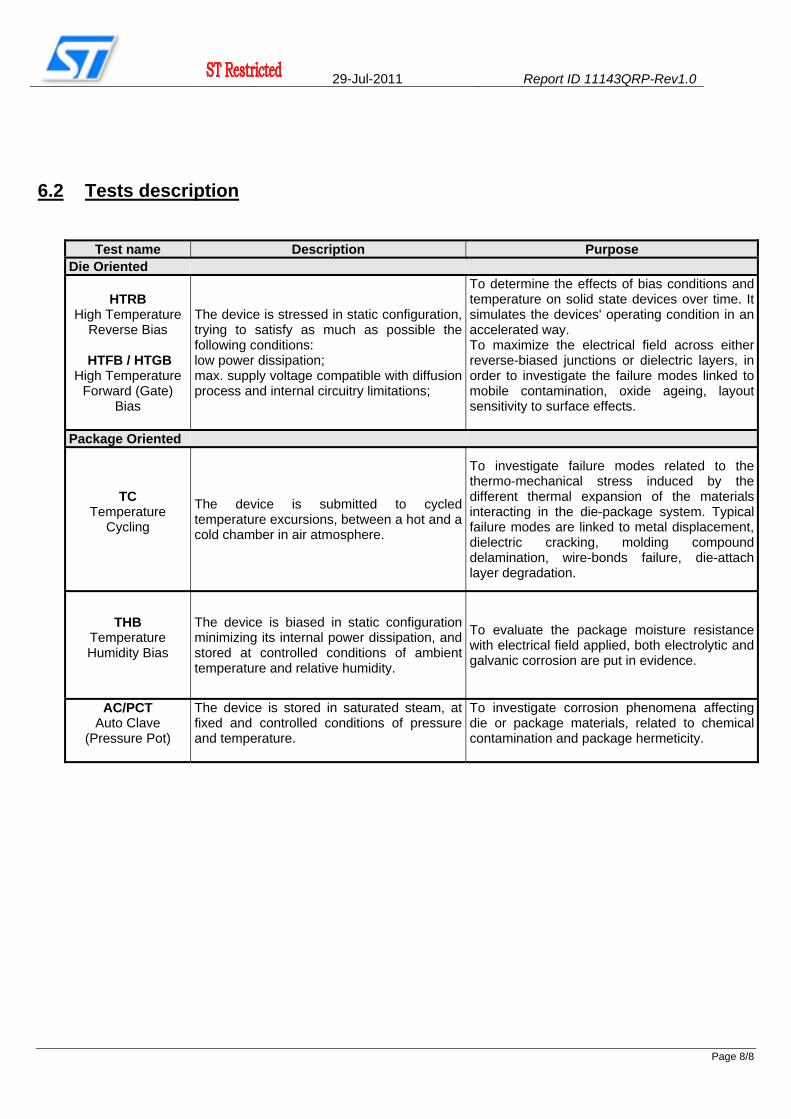
6.2 Tests description
Test name Description Purpose Die Oriented
HTRB High Temperature
Reverse Bias
HTFB / HTGB High Temperature
Forward (Gate) Bias
The device is stressed in static configuration, trying to satisfy as much as possible the following conditions: low power dissipation; max. supply voltage compatible with diffusion process and internal circuitry limitations;
To determine the effects of bias conditions and temperature on solid state devices over time. It simulates the devices' operating condition in an accelerated way. To maximize the electrical field across either reverse-biased junctions or dielectric layers, in order to investigate the failure modes linked to mobile contamination, oxide ageing, layout sensitivity to surface effects.
Package Oriented
TC Temperature
Cycling
The device is submitted to cycled temperature excursions, between a hot and a cold chamber in air atmosphere.
To investigate failure modes related to the thermo-mechanical stress induced by the different thermal expansion of the materials interacting in the die-package system. Typical failure modes are linked to metal displacement, dielectric cracking, molding compound delamination, wire-bonds failure, die-attach layer degradation.
THB Temperature Humidity Bias
The device is biased in static configuration minimizing its internal power dissipation, and stored at controlled conditions of ambient temperature and relative humidity.
To evaluate the package moisture resistance with electrical field applied, both electrolytic and galvanic corrosion are put in evidence.
AC/PCT Auto Clave
(Pressure Pot)
The device is stored in saturated steam, at fixed and controlled conditions of pressure and temperature.
To investigate corrosion phenomena affecting die or package materials, related to chemical contamination and package hermeticity.

Public Products List®
PCN Title : Selected Power Rectifiers//Additional Assembly and Test Location in China for D2PAK package PCN Reference : IPG-DIS/14/8398 PCN Created on : 20-MAR-2014
Subject : Public Products List
Dear Customer,
Please find below the Standard Public Products List impacted by the change:
ST COMMERCIAL PRODUCT
STPS10150CG-TR STPS10170CG-TR STPS10H100CG-TR STPS10L25G-TR STPS10L40CG-TR STPS10M80CG-TR STPS10SM80CG-TR STPS1545CG-TR STPS1545G STPS1545G-TR STPS15M80CG-TR STPS15SM80CG-TR STPS16170CG-TR STPS16H100CG-TR STPS20150CG STPS20150CG-TR STPS20170CG-TR STPS2045CG-TR STPS20H100CG STPS20H100CG-TR STPS20L15G-TR STPS20L45CG-TR STPS20M100SG-TR STPS20M80CG-TR STPS20SM100SG-TR STPS20SM60CG-TR STPS20SM60SG-TR STPS20SM80CG-TR STPS2545CG-TR STPS30150CG-TR STPS30170CG-TR STPS3045CG-TR STPS30SM100SG-TRSTPS30SM80CG-TR STPS745G-TR STPS8H100G STPS8H100G-TR STTH1002CG-TR STTH10R04G-TR STTH1302CG-TR STTH1602CG-TR STTH16R04CG-TR STTH2002CG STTH2002CG-TR STTH2002G-TR STTH2003CG STTH2003CG-TR STTH20L03CG-TR STTH20R04G-TR STTH802G STTH802G-TR STTH803G-TR STTH8R04G-TR
1/1

Please Read Carefully:
Information in this document is provided solely in connection with ST products. STMicroelectronics NV and its subsidiaries(‘‘ST’’) reserve theright to make changes, corrections, modifications or improvements, to this document, and the products and services described herein at anytime, without notice.
All ST products are sold pursuant to ST’s terms and conditions of sale.
Purchasers are solely responsible for the choice, selection and use of the ST products and services described herein, and ST assumes noliability whatsoever relating to the choice, selection or use of the ST products and services described herein.
No license, express or implied, by estoppel or otherwise, to any intellectual property rights is granted under this document. If any part of thisdocument refers to any third party products or services it shall not be deemed a license grant by ST for the use of such third party productsor services, or any intellectual property contained therein or considered as a warranty covering the use in any manner whatsoever of suchthird party products or services or any intellectual property contained therein.
UNLESS OTHERWISE SET FORTH IN ST’S TERMS AND CONDITIONS OF SALE ST DISCLAIMS ANY EXPRESS OR IMPLIEDWARRANTY WITH RESPECT TO THE USE AND / OR SALE OF ST PRODUCTS INCLUDING WITHOUT LIMITATION IMPLIEDWARRANTIES OF MERCHANTABILITY, FITNESS FOR A PARTICULAR PURPOSE ( AND THEIR EQUIVALENTS UNDER THE LAWSOF ANY JURISDICTION ), OR INFRINGEMENT OF ANY PATENT, COPYRIGHT OR OTHER INTELLECTUAL PROPERTY RIGHT.
ST PRODUCTS ARE NOT DESIGNED OR AUTHORIZED FOR USE IN: (A) SAFETY CRITICAL APPLICATIONS SUCH AS LIFESUPPORTING, ACTIVE IMPLANTED DEVICES OR SYSTEMS WITH PRODUCT FUNCTIONAL SAFETY REQUIREMENTS;(B) AERONAUTIC APPLICATIONS; (C) AUTOMOTIVE APPLICATIONS OR ENVIRONMENTS, AND/OR (D) AEROSPACEAPPLICATIONS OR ENVIRONMENTS. WHERE ST PRODUCTS ARE NOT DESIGNED FOR SUCH USE, THE PURCHASER SHALLUSE PRODUCTS AT PURCHASER’S SOLE RISK, EVEN IF ST HAS BEEN INFORMED IN WRITING OF SUCH USAGE, UNLESS APRODUCT IS EXPRESSLY DESIGNATED BY ST AS BEING INTENDED FOR ‘‘AUTOMOTIVE, AUTOMOTIVE SAFETY OR MEDICAL’’INDUSTRY DOMAINS ACCORDING TO ST PRODUCT DESIGN SPECIFICATIONS. PRODUCTS FORMALLY ESCC, QML ORJAN QUALIFIED ARE DEEMED SUITABLE FOR USE IN AEROSPACE BY THE CORRESPONDING GOVERNMENTAL AGENCY.
RESTRICTIONS OF USE AND CONFIDENTIALITY OBLIGATIONS:
THIS DOCUMENT AND ITS ANNEXES CONTAIN ST PROPRIETARY AND CONFIDENTIAL INFORMATION. THE DISCLOSURE,DISTRIBUTION, PUBLICATION OF WHATSOEVER NATURE OR USE FOR ANY OTHER PURPOSE THAN PROVIDED IN THISDOCUMENT OF ANY INFORMATION CONTAINED IN THIS DOCUMENT AND ITS ANNEXES IS SUBMITTED TO ST PRIOR EXPRESS AUTHORIZATION. ANY UNAUTHORIZED REVIEW, USE, DISCLOSURE OR DISTRIBUTION OF SUCH INFORMATION ISEXPRESSLY PROHIBITED.
Resale of ST products with provisions different from the statements and/or technical features set forth in this document shall immediately voidany warranty granted by ST for the ST product or service described herein and shall not create or extend in any manner whatsoever, anyliability of ST.
ST and the ST logo are trademarks or registered trademarks of ST in various countries.
Information in this document supersedes and replaces all information previously supplied.
The ST logo is a registered trademark of STMicroelectronics. All other names are the property of their respective owners
c 2014 STMicroelectronics - All rights reserved.
STMicroelectronics group of companies
Australia - Belgium - Brazil - Canada - China - Czech Republic - Finland - France - Germany - Hong Kong - India - Israel - Italy - Japan -
Malaysia - Malta - Morocco - Philippines - Singapore - Spain - Sweden - Switzerland - United Kingdom - United States of America
www.st.com