Product Specification T700A04X00 - Crystal Clear … -T400A01X00_REV2/7.0... · Product...
32
Product Specification T700A04X00 (REVISION 3) Crystal Clear Technology Sdn. Bhd. 16 Jalan TP5, Taman Perindustrian Sime UEP, 47600 Subang Jaya, Selangor DE Tel: +603-80247099 Website: www.cct.com.my _____________________________________________________________________________________
Transcript of Product Specification T700A04X00 - Crystal Clear … -T400A01X00_REV2/7.0... · Product...

Product Specification
T700A04X00
(REVISION 3)
Crystal Clear Technology Sdn. Bhd. 16 Jalan TP5, Taman Perindustrian Sime UEP,
47600 Subang Jaya, Selangor DE
Tel: +603-80247099
Website: www.cct.com.my
_____________________________________________________________________________________

CRYSTAL CLEAR TECHNOLOGY SDN. BHD Spec No. T700A04X00 REV3
1
1.0 Table of Contents
No Title Page
1 Table of Contents 1
2 Record of revision 2
3 General Specification 3
4 Absolute Maximum Ratings 4
5 Electrical Characteristics and Instruction Code 5
6 Optical Characteristics 9
7 Signal Timing Specification 13
8 Power Sequence 16
9 RA Test Condition 17
10 Inspection Criteria 18
11 Precaution and Limited Warranty 19
12 Mechanical Specification 23
13 Attachment:-
1. Capacitive touch panel – TP0085

CRYSTAL CLEAR TECHNOLOGY SDN. BHD Spec No. T700A04X00 REV3
2
2.0 Records of Revision
Rev Date Item Page Comment Originator Checked By 1.0 2.0 3.0
25.11.15 21.12.16 21.04.17
Initial Release Revise drawing Revise drawing T700A04C00C
- CTP pin out
Azhar Adam
Azhar
Liew Azhar
Azhar

CRYSTAL CLEAR TECHNOLOGY SDN. BHD Spec No. T700A04X00 REV3
3
3.0 General Specification T700A04X00 is a color active matrix TFT LCD module using amorphous
silicon TFT's (Thin Film Transistors) as an active switching devices. This module has
a 7.0inch diagonally measured active area with WSVGA resolutions (1024 horizontal
by 600 vertical pixel array). Each pixel is divided into RED, GREEN, BLUE dots
which are arranged in vertical stripe and this module can display 16.7M colors. The
TFT-LCD panel used for this module is adapted for a low reflection and higher color
type.
Item Contents Unit Note
LCD Type 7.0” TFT -
Display color 16.7M - 1
Viewing Direction (Optimum View)
All angle -
Operating temperature -20~+65 ℃
Storage temperature -30~+80 ℃
Module size 164.05 x 100.86 x 2.35 mm 2
Active Area (W×H) 153.6 x 90.0 mm
Number of Dots 1024(RGB) × 600 dots
Controller - -
Backlight 20 White LEDs pcs
Brightness 400 (typ) cd/m2
Interface Mode LVDS -
Technology Type a-Si
Surface Treatment 3H HC + LR -
Note 1: Color tone is slightly changed by temperature and driving voltage. Note 2: FPC or wire are not included.
CRYSTAL CLEAR TECHNOLOGY SDN. BHD Spec No. T700A04X00 REV3
4
4.0 Absolute Maximum Ratings 4.1 Electrical Absolute Maximum ratings (Vss = 0V, Ta = 25°C)
Item Symbol Min. Max. Unit Note
Power Supply Voltage VDD -0.3 4.2 V
1, 2 Power Supply for LED VLED -0.3 40 V
Notes:
1. If the module is above these absolute maximum ratings. It may become permanently damaged.
2. VDD >VSS must be maintained. 3. Please be sure users are grounded when handing LCD Module.
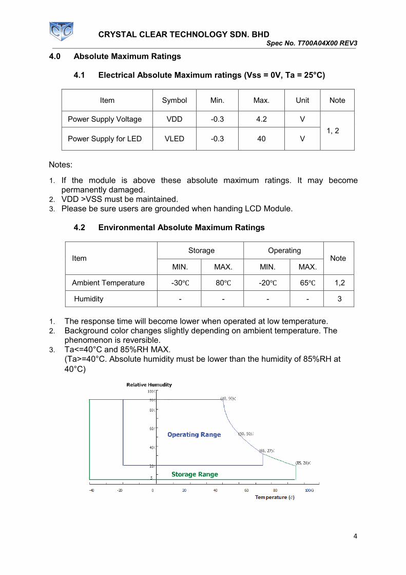
4.2 Environmental Absolute Maximum Ratings
Item Storage Operating
Note MIN. MAX. MIN. MAX.
Ambient Temperature -30℃ 80℃ -20℃ 65℃ 1,2
Humidity - - - - 3
1. The response time will become lower when operated at low temperature. 2. Background color changes slightly depending on ambient temperature. The
phenomenon is reversible. 3. Ta<=40°C and 85%RH MAX.
(Ta>=40°C. Absolute humidity must be lower than the humidity of 85%RH at
40°C)

CRYSTAL CLEAR TECHNOLOGY SDN. BHD Spec No. T700A04X00 REV3
5
5.0 Electrical Characteristics and Instruction Code
5.1 Electrical Characteristics (Vss = 0V, Ta = 25°C)
Notes:
1. The supply voltage is measured and specified at the interface connector of
LCM. The current draw and power consumption specified is for 3.7V at 25°C
2. Calculated value for reference (VLED X ILED)
3. CTF of Power Supply Current: PD /PBL
CRYSTAL CLEAR TECHNOLOGY SDN. BHD Spec No. T700A04X00 REV3
6
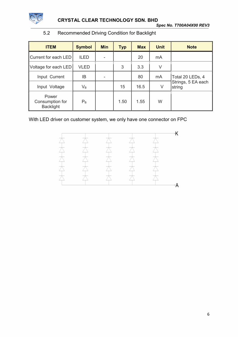
5.2 Recommended Driving Condition for Backlight
ITEM Symbol Min Typ Max Unit Note
Current for each LED ILED - 20 mA
Voltage for each LED VLED 3 3.3 V
Input Current IB - 80 mA Total 20 LEDs, 4 Strings, 5 EA each string Input Voltage VB 15 16.5 V
Power Consumption for
Backlight PB 1.50 1.55 W
With LED driver on customer system, we only have one connector on FPC
K
A
CRYSTAL CLEAR TECHNOLOGY SDN. BHD Spec No. T700A04X00 REV3
7
5.3 Interface Connection
The electronics interface connector is PF030-B31B-N09 5.3.1 The connector pin assignment are listed below:-
No. Symbol Description
1 VDDIN
Power Supply VDDIN = 3.7V (typ)
2 VDDIN
3 VDDIN
4 VDDIN
5 VDDIN
6 VDDIN
7 VDDIN
8 NC No connection
9 NC No connection
10 NC No connection
11 GND Ground
12 GND Ground
13 RIN0- -LVDS differential data input
14 RIN0+ +LVDS differential data input
15 GND Ground
16 RIN1- -LVDS differential data input
17 RIN1+ +LVDS differential data input
18 GND Ground
19 RIN2- -LVDS differential data input
20 RIN2+ +LVDS differential data input
21 GND Ground
22 LVDS_CLK- -LVDS differential clock input
23 LVDS_CLK+ +LVDS differential clock input
24 GND Ground
25 RIN3- -LVDS differential clock input
26 RIN3+ +LVDS differential clock input
27 GND Ground
28 LED_EN LED Enable
29 GND Ground
30 DVDDT Only for SEC test. Other customers NC
31 GND Ground

CRYSTAL CLEAR TECHNOLOGY SDN. BHD Spec No. T700A04X00 REV3
8
5.3.2 LVDS Interface
5.3.3 LVDS Input Signal
5.3.4 Data Input Format
Display Position of Input Data (V-H)

CRYSTAL CLEAR TECHNOLOGY SDN. BHD Spec No. T700A04X00 REV3
9
6.0 Optical Characteristics
Items Symbol Condition Min Typ Unit Remark
Response Time Tr + Tf
Θ = 0°
Ø = 0°
Ta = 25°C
- 30 - ms Note5
Contrast Ratio Cr 700 900 - - Note4
Uniformity Δ
White 70 - - % Note2
Surface Luminance Lv 340 400 - cd/m2 Note1
Viewing Angle
θ3 = 90
CR>10
- 80 -
° Note3 θ9 = 270 - 80 -
θ12 = 0 - 80 -
θ6 = 180 - 80 -
CIE (X, Y)
Chromaticity
White XW
Θ = 0°
Ø = 0°
Ta = 25°C
-0.02
0.303
+0.02
-
Note6
YW 0.333 -
Red XR 0.600 -
YR 0.340 -
Green XG 0.345 -
YG 0.565 -
Blue XB 0.145 -
YB 0.125 -
Gamma Scale 2.0 2.2 2.4
Note: The parameter is slightly changed by temperature, driving voltage and materiel

CRYSTAL CLEAR TECHNOLOGY SDN. BHD Spec No. T700A04X00 REV3
10
Note 1: The data are measured after LEDs are turned on for 5 minutes. LCM displays full white. The brightness is the average value of 9 measured spots. Measurement equipment PR-705 (Φ8mm) Measuring condition: - Measuring surroundings: Dark room.
- Measuring temperature: Ta=25℃.
- Adjust operating voltage to get optimum contrast at the center of the display. Measured value at the center point of LCD panel after more than 5 minutes while backlight turning on.
Note 2: The luminance uniformity is calculated by using following formula. ⊿Bp = Bp (Min.) / Bp (Max.)×100 (%)
Bp (Max.) = Maximum brightness in 9 measured spots Bp (Min.) = Minimum brightness in 9 measured spots.

CRYSTAL CLEAR TECHNOLOGY SDN. BHD Spec No. T700A04X00 REV3
11
Note 3: The definition of viewing angle: Refer to the graph below marked by θ and Ф
Note 4: Definition of contrast ratio. (Test LCD using DMS501)
Contrast ratio (Cr) = Brightness of selected dots
Brightness of non−selected dots
Note 5: Definition of Response time. (Test LCD using DMS501):
The output signals of photo detector are measured when the input signals are
changed from “black” to “white” (falling time) and from “white” to “black”(rising time),
respectively. The response time is defined as the time interval between the 10% and
90% of amplitudes. Refer to figure as below.

CRYSTAL CLEAR TECHNOLOGY SDN. BHD Spec No. T700A04X00 REV3
12
Note 6: Definition of Color of CIE Coordinate and NTSC Ratio.
Note 7: Definition of cross talk.
Cross talk ratio (%) = [pattern A Brightness-pattern B Brightness]/pattern A
Electric volume value = 3F+/-3Hex
CRYSTAL CLEAR TECHNOLOGY SDN. BHD Spec No. T700A04X00 REV3
13
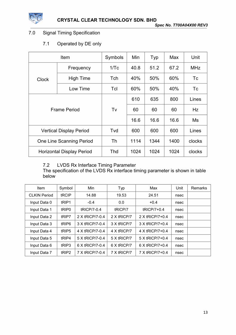
7.0 Signal Timing Specification 7.1 Operated by DE only
Item Symbols Min Typ Max Unit
Clock
Frequency 1/Tc 40.8 51.2 67.2 MHz
High Time Tch 40% 50% 60% Tc
Low Time Tcl 60% 50% 40% Tc
Frame Period Tv
610 635 800 Lines
60 60 60 Hz
16.6 16.6 16.6 Ms
Vertical Display Period Tvd 600 600 600 Lines
One Line Scanning Period Th 1114 1344 1400 clocks
Horizontal Display Period Thd 1024 1024 1024 clocks
7.2 LVDS Rx Interface Timing Parameter The specification of the LVDS Rx interface timing parameter is shown in table below
Item Symbol Min Typ Max Unit Remarks
CLKIN Period tRCIP 14.88 19.53 24.51 nsec
Input Data 0 tRIP1 -0.4 0.0 +0.4 nsec
Input Data 1 tRIP0 tRICP/7-0.4 tRICP/7 tRICP/7+0.4 nsec
Input Data 2 tRIP7 2 X tRICP/7-0.4 2 X tRICP/7 2 X tRICP/7+0.4 nsec
Input Data 3 tRIP6 3 X tRICP/7-0.4 3 X tRICP/7 3 X tRICP/7+0.4 nsec
Input Data 4 tRIP5 4 X tRICP/7-0.4 4 X tRICP/7 4 X tRICP/7+0.4 nsec
Input Data 5 tRIP4 5 X tRICP/7-0.4 5 X tRICP/7 5 X tRICP/7+0.4 nsec
Input Data 6 tRIP3 6 X tRICP/7-0.4 6 X tRICP/7 6 X tRICP/7+0.4 nsec
Input Data 7 tRIP2 7 X tRICP/7-0.4 7 X tRICP/7 7 X tRICP/7+0.4 nsec

CRYSTAL CLEAR TECHNOLOGY SDN. BHD Spec No. T700A04X00 REV3
14
* Vdiff = (RXO/Ez+)-(RXO/Ez-),f. ,(RXO/ECLK+)-(RXO/ECLK-)
7.3 Signal Timing Waveforms of Interface Signal

CRYSTAL CLEAR TECHNOLOGY SDN. BHD Spec No. T700A04X00 REV3
15
7.4 Input signals, basic display colors and grey scale of colors
CRYSTAL CLEAR TECHNOLOGY SDN. BHD Spec No. T700A04X00 REV3
16
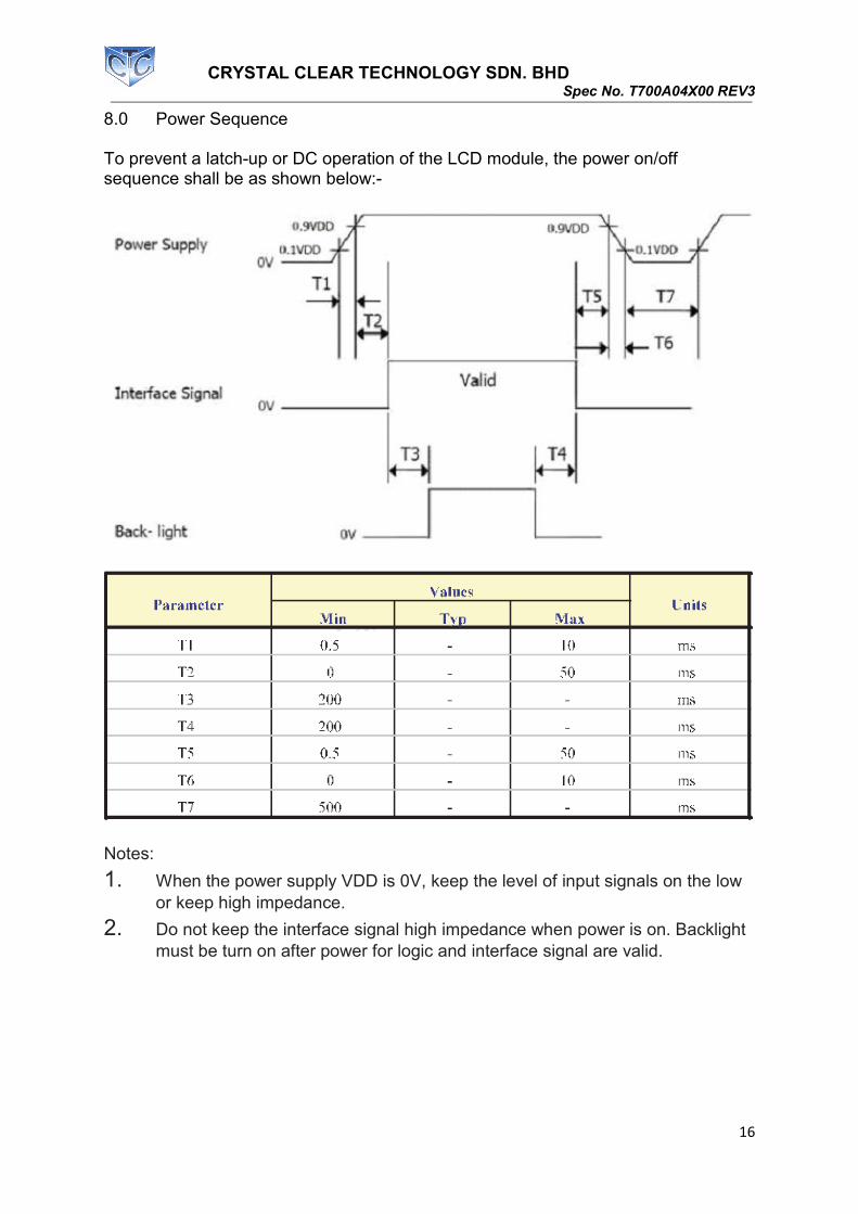
8.0 Power Sequence To prevent a latch-up or DC operation of the LCD module, the power on/off sequence shall be as shown below:-
Notes:
1. When the power supply VDD is 0V, keep the level of input signals on the low
or keep high impedance.
2. Do not keep the interface signal high impedance when power is on. Backlight
must be turn on after power for logic and interface signal are valid.

CRYSTAL CLEAR TECHNOLOGY SDN. BHD Spec No. T700A04X00 REV3
17
9.0 Reliability Test Condition
Item Test Condition
Operating
High Temperature 65degC, 240 hrs
Low Temperature -20degC,240 hrs
Storage
High Temperature 80degC, 240hrs and recovery for 2hrs
Low Temperature -30degC, 240hrs and recovery for 2hrs
High Temperature and High Humidity
50degC, 90%RH, 240hrs and recovery for 2 hrs
Thermal
Cycle RT � 30degC � Rt � 80degC � RT 0min 30min 5min 30min 5min 50 cycles (Power off)
Shock RT � 30degV � 80degC 0min 30min 30min 50 cycles (Power off)
Note: Rt means Room temperature

CRYSTAL CLEAR TECHNOLOGY SDN. BHD Spec No. T700A04X00 REV3
18
10.0 Inspection Criteria No Defect Definition of defect Inspection Criteria
1
a) Definition of dot
The size of defective dot over ½ of whole is regards as one defective dot. Smaller than ½ Larger than ½
‘No dot defect’ ‘1 dot defect’ (ignore) (counted)
A – Viewing area B – Viewing area C – Outside Viewing area
b) Bright Dot
Dot appear bright and unchanged in size when LCD panel is displaying black pattern Defect A B C
Bright Dot 1 1
NC Dark Dot 2 2
Total 4
NC – Not Count
c) Dark Dot
Dot appear dark and unchanged in size when LCD panel is displaying pure color (RED, GREEN or BLUE) pattern
d) 2 dot adjacent
1 pair = 2 dots
Type 1 Type 2
or Type 3
Defect Acc. Count
2 Bright dot Adjacent 0
2 Dark dot Adjacent 1
2
Black spot White Spot Bright spot Pin Hole Foreign Particle
-Black/Dark/Bright Spot is points on display which appear dark/bright and usually result from contamination - These defect do not vary in size intensity (contrast) when contras is varied.
Defect Category A B
D < 0.10 NC
NC 0.10 ≤ D ≤ 0.20 2
0.20 ≤ D ≤ 0.30 1
D > 0.30 0
3
Black Line White line Particle between POL and Glass Scratch on Glass
Defect Category A B
W < 0.03 NC
NC 0.03 ≤ W ≤ 0.08, L ≤2.0 2
W > 0.08 0
4
POL Bubble POL Dented
Defect Category A B
D < 0.20 NC
NC 0.20 ≤ D ≤ 0.30 3
0.30 ≤ D ≤ 0.50 2
D > 0.5 0
5 Mura (50% Grey)
Judged by Limit sample

CRYSTAL CLEAR TECHNOLOGY SDN. BHD Spec No. T700A04X00 REV3
19
11.0 Precaution and Limited Warranty
1. Handing Precautions a. The display panel is made of glass and polarizer. As glass is fragile. It tends to chip
during handling especially on the edges. Please avoid dropping or jarring. Do not subject it to a mechanical shock of impact or by dropping it.
b. If the display panel is damaged and the liquid crystal substance leaks out, be sure not to get any in your mouth. If the substance is in contact with your skin or clothes, wash it off using soap and water.
c. Do not apply excessive force to the display surface or the adjoining areas since this may cause the color tone to vary. Do not touch the display with bare hands. This will stain the display area and degrade the insulation between terminals. Scratch and dents may occur on polarizer too.
d. The polarizer covering the display surface of the LCD module is soft and easily scratched. Handle this polarizer carefully. Do not touch, push or rub the exposed polarizers with anything harder than a HB pencil lead (glass, tweezers, etc.). Do not put or attach anything on the display area to avoid leaving marks on it. Condensation on the surface and contact with terminals due to cold will damage, stain or dirty the polarizer. After products are tested at low temperature they must be warmed up in a container before coming in to contact with room temperature air.
e. If the display surface becomes contaminated, breathe on the surface and gently wipe it with a soft dry cloth. If it is heavily contaminated, moisten cloth with one of the following solvents
- Isopropyl alcohol - Ethyl alcohol - Do not scrub hard to avoid damaging the display surface.
f. Solvents other than those above-mentioned may damage the polarizer. Especially, do not use the following.
- Water - Ketone - Aromatic solvents - Wipe off saliva or water drops immediately, contact with water over a long
period of time may cause deformation or colour fading. Avoid contact with oil and fats.
g. Exercise care to minimize corrosion of the electrode. Corrosion of the electrodes is accelerated by water droplets, moisture condensation or a current flow in a high-humidity environment.
h. Install the LCD Module by using the mounting holes. When mounting the LCD module make sure it is free of twisting, warping and distortion. In particular, do not forcibly pull or bend the I/O cable or the backlight cable.
i. Do not attempt to disassemble or process the LCD module. j. NC terminal should be open. Do not connect anything. k. If the logic circuit power is off, do not apply the input signals. l. Electro-Static Discharge Control. Since this module uses a CMOS LSI, the same
careful attention should be paid to electrostatic discharge as for an ordinary CMOS IC. To prevent destruction of the elements by static electricity, be careful to maintain an optimum work environment.
- Before removing LCM from its packing case or incorporating it into a set, be sure the module and your body have the same electric potential. Be sure to ground the body when handling the LCD modules.
- Tools required for assembly, such as soldering irons, must be properly grounded. Make certain the AC power source for the soldering iron does not leak. When using an electric screwdriver to attach LCM, the screw driver should be of ground potentiality to minimize as much as possible any

CRYSTAL CLEAR TECHNOLOGY SDN. BHD Spec No. T700A04X00 REV3
20
transmission of electromagnetic waves produced sparks coming from the commutator of the motor.
- To reduce the amount of static electricity generated, do not conduct assembly and other work under dry conditions. To reduce the generation of static electricity be careful that the air in the work environment is not too dry. A relative humidity of 50%-60% is recommended. As far as possible make the electric potential of your work clothes and that of the work bench the ground potential.
- The LCD module is coated with a film to protect the display surface. Exercise care when peeling off this protective film since static electricity may be generated.
m. Since LCM has been assembled and adjusted with a high degree of precision, avoid applying excessive shocks to the module or making any alterations or modifications to it.
- Do not alter, modify or change the shape of the tab on the metal frame. - Do not make extra holes on the printed circuit board, modify its shape or
change the positions of components to be attached. - Do not damage or modify the pattern writing on the printed circuit board. - Absolutely do not modify the zebra rubber strip (conductive rubber) or heat
seal connector. - Except for soldering the interface, do not make any alterations or
modifications with a soldering iron. - Do not drop, bend or twist the LCM.
2. Storage Precautions When storing the LCD modules, the following precaution are necessary.
a. Store them in a sealed polyethylene bag. If properly sealed, there is no need for the desiccant.
b. Store them in a dark place. Do not expose to sunlight or fluorescent light, keep the temperature between 0C and 35C, and keep the relative humidity between 40%RH and 60%RH.
c. The polarizer surface should not come in contact with any other objects.
3. Others a. Liquid crystals solidify under low temperature (below the storage temperature range)
leading to defective orientation or the generation of air bubbles (black or white). Air bubbles may also be generated if the module is subject to a low temperature.
b. If the LCD modules have been operating for a long time showing the same display patterns, the display patterns may remain on the screen as ghost images and a slight contrast irregularity may also appear. A normal operating status can be regained by suspending use for some time. It should be noted that this phenomenon does not adversely affect performance reliability.
c. To minimize the performance degradation of the LCD modules resulting from destruction caused by static electricity etc. Exercise care to avoid holding the following sections when handling the modules.
Exposed area of the printed circuit board.
Terminal electrode sections.
4. Using LCD Modules a. Installing LCD Modules
The hole in the printed circuit board is used to fix LCM as shown in the picture
below.
Attend to the following items when installing the LCM.

CRYSTAL CLEAR TECHNOLOGY SDN. BHD Spec No. T700A04X00 REV3
21
b. Cover the surface with a transparent protective plate to protect the polarizer and LC cell.
c. When assembling the LCM into other equipment, the spacer to the bit between the LCM and the fitting plate should have enough height to avoid causing stress to the module surface, refer to the individual specifications for measurements. The measurement tolerance should be 0.1mm.
d. Precaution for assemble the module with BTB connector: Please note the position of the male and female connector position, don’t
assemble or assemble like the method which the following picture shows
5. Precaution for soldering the LCM
Manual soldering Machine drag
soldering
Machine press
soldering
No RoHS
Product
290°C ~350°C.
Time: 3-5S.
330°C ~350°C.
Speed: 4-8 mm/s.
300°C ~330°C.
Time: 3-6S.
Press: 0.8~1.2Mpa
RoHS
Product
340°C ~370°C.
Time: 3-5S.
350°C ~370°C.
Time: 4-8 mm/s.
330°C ~360°C.
Time: 3-6S.
Press: 0.8~1.2Mpa
a. If soldering flux is used, be sure to remove any remaining flux after finishing the soldering operation (This does not apply in the case of a non-halogen type of flux). It is recommended that you protect the LCD surface with a cover during soldering to prevent any damage due to flux spatters.
b. When soldering the electroluminescent panel and PC board, the panel and board should not be detached more than three times. This maximum number is determined by the temperature and time conditions mentioned above, though there may be some variance depending on the temperature of the soldering iron.
c. When removing the electroluminescent panel from the PC board, be sure the solder has completely melted, the soldered pad on the PC board could be damaged.

CRYSTAL CLEAR TECHNOLOGY SDN. BHD Spec No. T700A04X00 REV3
22
6. Precautions for Operation a. Viewing angle varies with the change of liquid crystal driving voltage (VLCD).
Adjust VLCD to show the best contrast. b. It is recommended to drive LCD's within the specified voltage limit since over limit
will cause shorter LCD life. An electrochemical reaction due to direct current causes LCD deterioration. Avoid the use of direct current drive.
c. Response time will be extremely delayed at lower temperature compared to room operating temperature range and on the other hand, at higher temperature LCD shows dark color in them. However those phenomena do not mean malfunction. The LCD will return to normal performance when ambient temperature revert to room condition.
d. If the display area is pushed hard during operation, the display will become abnormal. However, it will return to normal if it is turned off and on.
e. A slight dew depositing on terminals is a cause for electro-chemical reaction resulting in terminal open circuit.
f. Input logic voltage before apply analogue high voltage such as LCD driving voltage when power on. Remove analogue high voltage before logic voltage when power off the module. Input each signal after the positive/negative voltage becomes stable.
g. Please keep the temperature within the specified range for use and storage. Polarization degradation, bubble generation or polarizer peel-off may occur with high temperature and high humidity.
7. Safety a. It is recommended to crush damaged or unnecessary LCDs into pieces and wash
them off with solvents such as acetone and ethanol, which should later be burned. b. If any liquid leaks out of a damaged glass cell and comes in contact with the hands,
wash off thoroughly with soap and water.
8. Limited Warranty Unless otherwise agreed between Crystal Clear Technology and customer, Crystal Clear Technology will replace or repair any of its LCD and LCM which is found to be defective electrically and visually when inspected in accordance with Crystal Clear Technology acceptance standards, for a period of one year from date of shipment. Confirmation of such date shall be based on freight documents. The warranty liability of Crystal Clear Technology is limited to repair and/or replacement on the terms set forth above. Crystal Clear Technology will not responsible for any subsequent or consequential events.
9. Return LCM under Warranty
No warranty can be granted if the precautions stated above have been disregarded. The typical examples of violations are: - Broken LCD glass - PCB eyelet’s damaged or modified - PCB conductors damaged - Circuit modified in any way, including addition of components. - PCB tampered with by grinding, engraving or painting varnish. - Soldering to, or modifying the bezel in any manner. Module repairs will be invoiced to customer upon mutual agreement. Modules must be returned with sufficient description of failure or defects. Any connectors or cable installed by customer must be removed completely without damaging the PCB eyelet’s, conductors and terminals.
H
1 2 3 4 5 6
G
F
E
C
D
B
A
1 2 3 4 5 6
REMARKSNO MATERIALMODEL NAME
PART NAME
DRAWING NUMBER
16, JLN TP5, TMN PERINDUSTRIAN SIME UEP,
47500 SUBANG JAYA, SELANGOR DARUL EHSAN
CRYSTAL CLEAR TECHNOLOGY SDN BHD
CHECKED
7 8
Crystal-Clear Technology
APPROVED
AZHAR12-12-2016 NTS
UNIT : MM
9
DRAWNSHEET
MECHANICAL
SPECIFICATION
T700A04N00
10
H21
1
11
REV.
1G
F
E
C
D
B
7 8 9 10
A
11
NOTE:
1. GENERAL TOLERANCE TO BE ±0.3MM
2. DISPLAY 16.7M COLORS (HI FRC)
3. OPERATING VOLTAGE: 3.7V (TYP)
4. OPERATING TEMPERATURE: -20°C ~ -65°C
5. STORAGE TEMPERATURE: -40°C ~ -85°C
6. RoSH COMPLIANCE
7. ( ) INDICATED FOR REFERENCE AND REPEATED DIMENSION ONLY
31
SYMBOLPIN
302928272625242322212019181716151413121110987654321 VDDIN
NCNCNC
GNDGNDRIN0-RIN0+GNDRIN1-
RIN1+GND
RIN2-RIN2+GND
LVDS_CLK-
GNDRIN3-RIN3+GNDLED_EN
GNDDVDDTGND
PIN OUT TABLE
VDDINVDDINVDDINVDDINVDDINVDDIN
LVDS_CLK+
164.05±0.15 - OUTLINE
158.4 - TFT
157.8±0.3 - UP POL
153.6 - A/A
100.86±
0.15 - OUTLINE
97.2 - TFT
94.4 - CF
93.3±
0.3 - UP POL
90 - A/A
48.5
81.14.3
Active Area
(76.15)(28.75)
(22.21)
2.36±0.15
(26.23)
(14.5)
131
123.0±10.0
11.8±1.0
(66.56)
163.45
ADD FPC
ADAM 21/12/20162
2
2
2
(13.03)
FPC - PITCH 0.3mm
0.30
0.30
0.60
P0.3 X (31-1)=9.0±0.1
9.60±0.1
2.40
2
STIFFENERCONTACT SIDE
0.20±0.03
2
2
2

24
IC
153.6 - A/A
154.6 - V/A
90.0
- A
/A
91.0
- V
/A
11
7.2
±0.3
183.0±0.3
14.2
14.7
13.6
13.1
3.4±0.1
7.02±0.3
82
.38±1.0
45.87±0.5
(3.5)
41.1
(14.6
4)
(41.2
8)
(76.15)(37.3)
(22.2
1)
0.30
0.50
2.50
3.50
0.50
3.5
0
5.0
0
0.30±0.05
H
1 2 3 4 5 6
G
F
E
C
D
B
A
1 2 3 4 5 6
REMARKSNO MATERIALMODEL NAME
PART NAME
DRAWING NUMBER
16, JLN TP5, TMN PERINDUSTRIAN SIME UEP,
47500 SUBANG JAYA, SELANGOR DARUL EHSAN
CRYSTAL CLEAR TECHNOLOGY SDN BHD
CHECKED
7 8
Crystal-Clear Technology
APPROVED
AZHAR04-02-2016 NTS
UNIT : MM
9
DRAWNSHEET
MECHANICAL
SPECIFICATION
T700A04C00C
10
H31
1
11
REV.
1G
F
E
C
D
B
7 8 9 10
A
11
NOTE:
1. GENERAL TOLERANCE TO BE ±0.3MM
2. DISPLAY 16.7M COLORS (HI FRC)
3. OPERATING VOLTAGE: 3.7V (TYP)
4. OPERATING TEMPERATURE: -20°C ~ -65°C
5. STORAGE TEMPERATURE: -40°C ~ -85°C
6. RoSH COMPLIANCE
7. ( ) INDICATED FOR REFERENCE AND REPEATED
DIMENSION ONLY
31
SYMBOLPIN
302928272625242322212019181716151413121110987654321 VDDIN
NCNCNCGNDGNDRIN0-RIN0+GNDRIN1-
RIN1+GND
RIN2-RIN2+GND
LVDS_CLK-
GNDRIN3-RIN3+GNDLED_EN
GNDDVDDTGND
PIN OUT TABLE - TFT
VDDINVDDINVDDINVDDINVDDINVDDIN
LVDS_CLK+
(14.5)
(25.9
5)
(20.0)
SYMBOLPIN
54321
VDDVSSIRQSDASCL
PIN OUT TABLE - CTP
91.5
58.6
131
116.0
±10.0
11
.8±1.0
(76.95)
ADD FPC
ADAM 21/12/20162
2
2
2
(19.5
5)
FPC - PITCH 0.3mm
0.30
0.30
0.60
P0.3 X (31-1)=9.0±0.1
9.60±0.1
2.4
0
2
STIFFENERCONTACT SIDE
CONTACT SIDE
0.20±0.03
STIFFENER
2
2
2
6
RST
REVISE PIN TABLE - CTP
AZHAR 21-04-20173
3
Product Specification
TP0085
Crystal Clear Technology sdn. bhd. 16Jalan TP5—Taman Perindustrian Sime UEP
47600 Subang Jaya—Selangor DE
Malaysia. T: +603 80247099 F: +603 80247098
CRYSTAL CLEAR TECHNOLOGY SDN. BHD.
Spec. No: TP0085
1
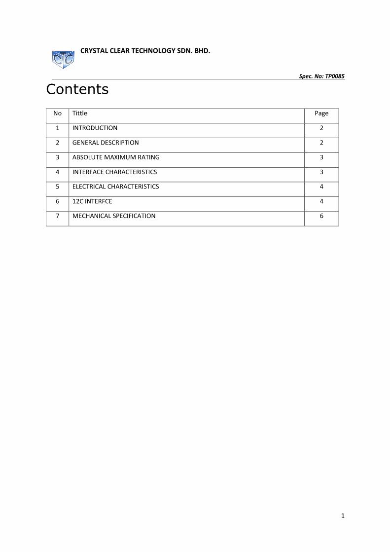
Contents
No Tittle Page
1 INTRODUCTION 2
2 GENERAL DESCRIPTION 2
3 ABSOLUTE MAXIMUM RATING 3
4 INTERFACE CHARACTERISTICS 3
5 ELECTRICAL CHARACTERISTICS 4
6 12C INTERFCE 4
7 MECHANICAL SPECIFICATION 6
CRYSTAL CLEAR TECHNOLOGY SDN. BHD.
Spec. No: TP0085
2
1. Introduction
The purpose of this specification is defined the general provision and
quality requirement apply to 7 inch Capacitive Touch module integrated by
Crystal Clear Technology. This document, together with the module drawing, is the highest level specification for this product. When users touch module by finger, the module can send coordinates of point at the contact point to host. The finger position information is sent to host by I2C bus which is
determined by host through IRQ line.
2. General Description
This document contains the Capacitive Touch module specification. The maximum rating, characteristics, hardware, and inspection of the module
are described in the subsequent sections. In special, I2C protocol will be introduced in detail.
2.1. Touch sensor characteristics
� Technology: Use the character of capacitive among the touch electrodes on touch panel to identify the positions of touch signals
� Touch method: Ten fingers multi touch with pressure sensing
� Interface: I2C
2.2. General Specification
Item Specification Unit
Screen Diagonal 7.0 Inch
Applied Resolution 800 x 480 pixel
Module Outline 100(H) x 164.1(W) x 1.4(T) (Excluded FPC) Mm
Touch Area (H) x (W) Mm
Cover Lens Material Glass -
Transparency 85 %
Origin - -
Controller GT911 -

CRYSTAL CLEAR TECHNOLOGY SDN. BHD.
Spec. No: TP0085
3
3. Absolute Maximum Ratings
Absolute Maximum rating of touch panel module is as following
Symbol Parameter Value Unit
VCORE Supply Voltage for Logic -0.3 to +2.8 V
VDDIO Supply Voltage for I/O -0.3 to +3.3 V
TA Operating Temperature -20 to +85 °C
TSTG Storage Temperature -30 to +85 °C
Note: If the module exceeds the absolute maximum ratings, it may be damaged
permanently. Also, if the module operated with the absolute maximum ratings for a long
time, its reliability may drop.
4. Electrical Characteristics
DC Characteristics (Unless otherwise specified, Voltage Referenced to VSS, TA = -20 to 85°C)
Symbol Parameter Conditions Min Typ Max Unit
AVDD Analog power supply 2.8 - 3.3 V
VDDIO Digital I/O power supply 1.8 - 3.3 V
IDD Operating mode current - 8 14.5 mA
IGR Green mode current - 3.3 - mA
Isleep Sleep mode current 70 - 120 uA
VOH1 Logic High Output Voltage 0.85*
VDDIO - - V
VOL1 Logic Low Output Voltage - - 0.15*
VDDIO V
VIH1 Logic High Input voltage
0.75*
VDDIO -
VDDIO
+3 V
VIL1 Logic Low Input voltage -0.3 - 0.25*
VDDIO V

CRYSTAL CLEAR TECHNOLOGY SDN. BHD.
Spec. No: TP0085
4
5. Pin Definition
No. Symbol I/O Function
1 RST I Sensor system global reset
2 VDD P Power supply
3 VSS P Ground
4 IRQ O Sensor data ready request
5 SDA I/O I2C serial data
6 SCL I I2C serial clock
6. I2C Interface
Touch panel is used as I2C Slave Device, I2C Slave address is 0x14.
6.1. Interface Diagram
The system block diagram is as shown in below. There are three
communication pins connected between CPU and Touch Panel Module which
are including external interrupt IRQ, I2C pins SCL and SDA. The IRQ is
active low while the touch state is calculated by Touch Panel Module and the
touch information can be translated via I2C communication interface. The
I2C data format, protocol and report packet are described as following.
Touch Panel Module
Host
CPU
Touch Screen
RST
IRQ
SCL
SDA
CRYSTAL CLEAR TECHNOLOGY SDN. BHD.
Spec. No: TP0085
5
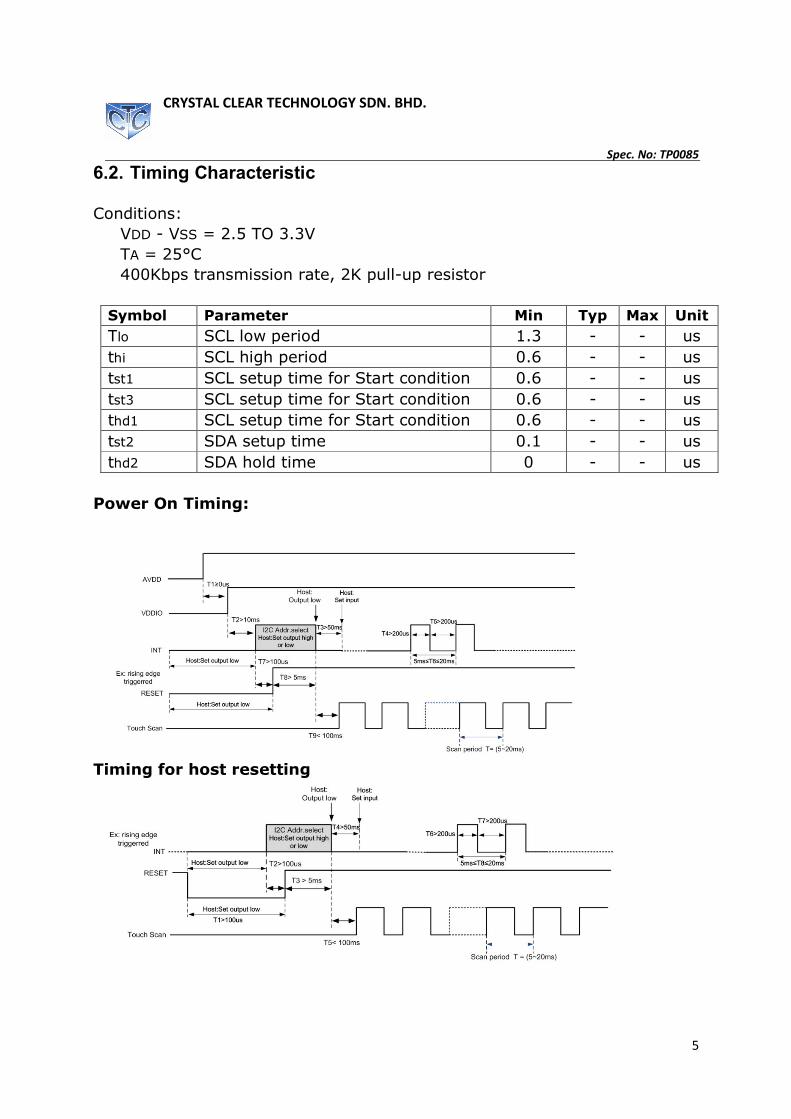
6.2. Timing Characteristic
Conditions:
VDD - VSS = 2.5 TO 3.3V
TA = 25°C
400Kbps transmission rate, 2K pull-up resistor
Symbol Parameter Min Typ Max Unit
Tlo SCL low period 1.3 - - us
thi SCL high period 0.6 - - us
tst1 SCL setup time for Start condition 0.6 - - us
tst3 SCL setup time for Start condition 0.6 - - us
thd1 SCL setup time for Start condition 0.6 - - us
tst2 SDA setup time 0.1 - - us
thd2 SDA hold time 0 - - us
Power On Timing:
Timing for host resetting