Product Portfolio - Nanofabrication systems for EBL … Downloads/Raith...• High kV lithography...
12
Product Portfolio
-
Upload
nguyenhuong -
Category
Documents
-
view
218 -
download
2
Transcript of Product Portfolio - Nanofabrication systems for EBL … Downloads/Raith...• High kV lithography...

Product Portfolio
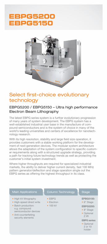
The latest EBPG series system is a further evolutionary progression of many years of system development. The EBPG system has a well-established industrial user base in the manufacture of com-pound semiconductors and is the system of choice in many of the world’s leading universities and centers of excellence for nanotech-nology research.
With its high resolution, stability and large field size operation, it pro vides customers with a stable working platform for the develop-ment of next-generation devices. The modular system architecture allows the adaptation of the system configuration to specific custom-er requirements along with a structured upgrade strategy, providing a path for tracking future technology trends as well as protecting the customer’s initial system investment.
Where higher throughputs are required for specialized industrial markets, the ability to deliver higher current density, fast 100 MHz pattern generator/deflection and stage operation single out the EBPG series as offering the highest throughput in its class.
Select first-choice evolutionary technologyEBPG5200 / EBPG5150 – Ultra high performance Electron Beam Lithography
• High kV lithography • High-speed direct write • Batch production:
e.g. compound semi conductor devices
• Anti-counterfeiting security elements
• EBPG• Electron• 100 kV
EPBG5150:• 6“ Stage
EBPG5200:• 8“ Stage• Optional
Z lift
EBPG series:• Optional
2 or 10 holder
Main Applications Column Technology Stage

EB
PG
DE
DIC
AT
ED
EL
EC
TR
ON
BE
AM
LIT
HO
GR
AP
HY
VO
YA
GE
R
VOYAGERTM is recommended for all industrial and academic Elec-tron Beam Lithography applications where the important objectives are high write throughput and high-resolution. As well as the newly developed, innovative eWRITE system architecture, Raith attaches great importance to an attractive price/performance ratio throughout the lifetime of the system.
The hardware and software have been consistently designed for auto-mated exposure operations. The state-of-the-art high-performance pattern generator and electron optics have been optimally aligned.
Samples of up to 8 inches are exposed at high speed. The neces-sary system stability is ensured, even in difficult environments, by a thermally stabilized and environmentally tolerant housing.
Speed up! – Fast, smart, innovative and economical VOYAGER – a new class of Electron Beam Lithography technology
• Nanolithography• High speed direct write • Diffractive optical
elements • Anti-counterfeiting
security elements • Small-batch compount
semiconductor devices manufacturing
• eWrite• Electron• 50 kV• High-speed ET SE
detector and high-speed post-lens BSE detector
• 6˝ full travel
• Large Z travel
Main Applications Column Technology Stage
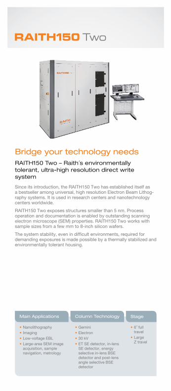
Since its introduction, the RAITH150 Two has established itself as a bestseller among universal, high resolution Electron Beam Lithog-raphy systems. It is used in research centers and nanotechnology centers worldwide.
RAITH150 Two exposes structures smaller than 5 nm. Process operation and documentation is enabled by outstanding scanning electron microscope (SEM) properties. RAITH150 Two works with sample sizes from a few mm to 8-inch silicon wafers.
The system stability, even in difficult environments, required for demanding exposures is made possible by a thermally stabilized and environmentally tolerant housing.
Bridge your technology needsRAITH150 Two – Raith´s environmentally tolerant, ultra-high resolution direct write system
• Nanolithography• Imaging• Low-voltage EBL• Large-area SEM image
acquisition, sample navigation, metrology
• Gemini• Electron• 30 kV• ET SE detector, in-lens
SE detector, energy selective in-lens BSE detector and post-lens angle selective BSE detector
• 6˝ full travel
• Large Z travel
Main Applications Column Technology Stage

RA
ITH
15
0 T
wo
DE
DIC
AT
ED
EL
EC
TR
ON
BE
AM
LIT
HO
GR
AP
HY
/ FIB
NA
NO
FA
BR
ICA
TIO
Nio
nL
INE
Plu
s
High-resolution and versatile nanofabrication employs advanced FIB techniques with lithography instrumentation.
ionLINE Plus breaks new ground for your nanofabrication challenges by realizing the synergy of a focused ion beam with mature lithog-raphy architecture. It combines direct FIB processing techniques with the unrivaled stability, automation, and high resolution of a lithography instrument. Featuring the latest-generation ion column, pattern generator, and software platform, ionLINE Plus offers unique capabilities for advanced FIB nanofabrication.
FIB techniques can make nanofabrication more efficient by employ-ing direct patterning (milling, deposition, etching) or hard masking. Moreover, IONselect technology offers a range of ions with excellent handling, opening the door for various nanofabrication techniques yet to be explored. It also supports processing by surface functional-ization or maskless ion implantation, paving the way for new break-throughs in next-generation research.
Finally, a range of options for extended functionalities like in-situ gas injection, nanoprobing or nanoprofilometry enhance the versatility of ionLINE Plus, while its highly configurable chamber and upgrade paths ensure the tool is future proof.
FIB nanofabrication at its excellenceionLINE Plus – FIB meets LITHO
• Direct and 3D nano-fabrication
• Nanolithography• Deposition and Gas
Assisted Etching • Nanoengineering
platform• Ga-free nanofabrication
• nanoFIBTM Three• Ion Ga (Au, Si, Ge) • 35 kV• IONselect
• 4˝ full travel
• Large Z travel
• Rotation and tilt sample holder
Main Applications Column Technology Stage

eLINE PlusTM is the optimum, widely distributed system for univer-sities and research centers that want to combine an efficient and uncompromising Electron Beam Lithography system with an open platform for further nano fabrication processes and techniques.
In order to be prepared for the broadest bandwidth of applications, modern nanotechnology research today requires multiple tech -niques beyond classic and pure Electron Beam Lithography (EBL) – preferentially in-situ.
In addition to fully integrated nanomanipulators and a mechanism for electron beam induced deposition and etching, a range of further options is available that identifies eLINE Plus as currently the most versatile and unique nanoengineering EBL system.
Discover nanoengineering beyond Electron Beam LithographyeLINE Plus – the swiss army knife for nano-fabrication
• Nanolithography• (Large-area) SEM image
acquisition, sample navigation, metrology
• Focused Electron Beam Induced Processes (FEBIP)
• Nanoprobing, nanomani-pulation, nanoprofilometry
• Material and structural analysis
• Customized applications using open platform concept
• Gemini • Electron• 30 kV • ET SE detector, in-lens
SE detector, energy selective in-lens BSE detector and post-lens angle selective BSE detector
• 4˝ full travel
• Large Z travel
• Rotation and tilt sample holder (option)
Main Applications Column Technology Stage
eL
INE
Plu
sM
ULT
I TE
CH
NIQ
UE
EL
EC
TR
ON
BE
AM
LIT
HO
GR
AP
HY
PIO
NE
ER
Tw
o
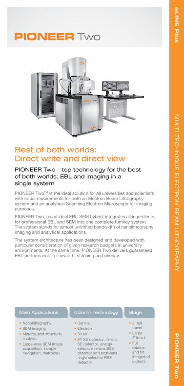
PIONEER TwoTM is the ideal solution for all universities and scientists with equal requirements for both an Electron Beam Lithography system and an analytical Scanning Electron Microscope for imaging pur poses.
PIONEER Two, as an ideal EBL-SEM hybrid, integrates all ingredients for professional EBL and SEM into one complete turnkey system. The system stands for almost unlimited bandwidth of nanolithography, imaging and analytical applications.
The system architecture has been designed and developed with particular consideration of given research budgets in university environments. At the same time, PIONEER Two delivers guaranteed EBL performance in linewidth, stitching and overlay.
Best of both worlds: Direct write and direct viewPIONEER Two – top technology for the best of both worlds: EBL and imaging in a single system
• Nanolithography • SEM imaging • Material and structural
analysis• Large-area SEM image
acquisition, sample navigation, metrology
• Gemini • Electron • 30 kV • ET SE detector, in-lens
SE detector, energy selective in-lens BSE detector and post-lens angle selective BSE detector
• 2˝ full travel
• Large Z travel
• Full rotation and tilt integrated (option)
Main Applications Column Technology Stage

Raith offers the ELPHYTM product family, a nanolithography upgrade kit, that enables scanning electron microscopes (SEMs), focused ion beam microscopes (FIBs), helium ion microscopes (HIMs), or combined systems (FIB-SEMs) to deliver professional nanolitho g-raphy applications.
This spectrum of solutions begins with ELPHY Quantum, the most widely distributed Raith SEM/FIB attachment in the market. The entire range of processes (CAD layout and processing, control of exposure parameters, remote control of each microscope etc.) is integrated within a single user interface, the Raith NanoSuite. The specially developed hardware is supplied on Windows-based PCs.
ELPHY Plus was developed for more demanding applications or on field-emission SEMs with higher current density and in connection with a Laser Interferometer Controlled Sample Stage. A well-engineered and fast pattern generator hardware delivers the required performance.
Raith has set new standards in the market for nanolithographic solutions (“Attachments”) with ELPHY MultiBeam. The ELPHY MultiBeam combines the latest technology for three-dimensional IBL and other 3D nanofabrication techniques with the very best EBL performance, and helps to exploit the full nanofabrication potential of any FIB-SEM or FIB system.
ELPHY – the easiest and most economical access to professional nanolithography and nanofabrication
• Nanolithography• SEM lithography• FIB-SEM lithography and nanopatterning• Helium Ion Microscopy –
HIM-lithography and nanopatterning• (3D) nanoprototyping• Attach to analytical SEM, FIB-SEM,
FIB, HIM supplier instrumentation
• Standard stage delivered by analytical SEM, FIB-SEM, FIB, HIM supplier
Main Applications Stage
Unlock the full nanopatterning potential of your SEM, FIB-SEM, or HIM
EL
PH
Y U
PG
RA
DE
KIT
SR
EV
ER
SE
EN
GIN
EE
RIN
G C
HIP
SC
AN
NE
R
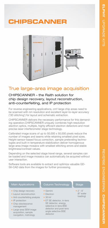
For reverse engineering applications, cm²-large chip areas need to be scanned with nm resolution and excellent layer-to-layer accuracy (‘3D stitching’) for layout and schematic extraction.
CHIPSCANNER delivers the necessary performance for this demand-ing operation.CHIPSCANNER uniquely combines high-resolution electron optics, multiple, highly efficient electron detectors and most precise laser interferometer stage technology.
Calibrated image scans of up to 50,000 x 50,000 pixels reduce the number of images and seams while retaining smallest pixel sizes. Height-sensor-based focus correction, sample preleveling techno-logies and built-in temperature stabilization deliver homogenous large-area image mosaics with smallest stitching errors and stable brightness/contrast values.
Depending on the selected stage travel range, several samples can be loaded and image mosaics can automatically be acquired without user interaction.
Software tools are available to extract and optimize valuable GD-SII-CAD data from the images for further processing.
True large-area image acquisitionCHIPSCANNER – the Raith solution for chip design recovery, layout reconstruction, anti-counterfeiting, and IP protection
• Chip design recovery• Layout reconstruction• Anti-counterfeiting analysis• IP protection• Chip obsolescence management• Large-area SEM image
acquisition, sample navigation, metrology
• Gemini• Electron• 30 kV• ET SE detector, in-lens
SE detector, energy selective in-lens BSE detector and post-lens angle selective BSE detector
• 2˝ - 6˝ (8˝ wafer loading)
Main Applications Column Technology Stage
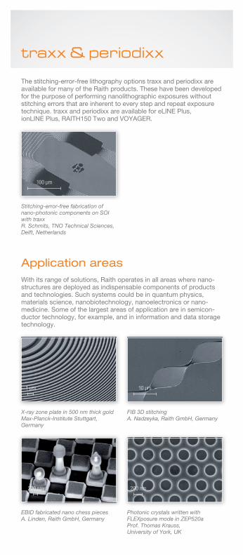
The stitching-error-free lithography options traxx and periodixx are available for many of the Raith products. These have been developed for the purpose of performing nanolithographic exposures without stitching errors that are inherent to every step and repeat exposure technique. traxx and periodixx are available for eLINE Plus, ionLINE Plus, RAITH150 Two and VOYAGER.
With its range of solutions, Raith operates in all areas where nano-structures are deployed as indispensable components of products and technologies. Such systems could be in quantum physics, materials science, nanobiotechnology, nanoelectronics or nano-medicine. Some of the largest areas of application are in semicon-ductor technology, for example, and in information and data storage technology.
Application areas
X-ray zone plate in 500 nm thick goldMax-Planck-Institute Stuttgart, Germany
1 µm
Photonic crystals written with FLEXposure mode in ZEP520a Prof. Thomas Krauss, University of York, UK
200 nm
Stitching-error-free fabrication of nano-photonic components on SOI with traxxR. Schmits, TNO Technical Sciences, Delft, Netherlands
100 µm
FIB 3D stitchingA. Nadzeyka, Raith GmbH, Germany
10 µm
EBID fabricated nano chess pieces A. Linden, Raith GmbH, Germany
200 nm

Founded in 1980 and headquartered in Dortmund, Germany, Raith employs around 200 people. The company works as closely as pos-sible with customers in the most important global markets through subsidiaries in the Netherlands, the USA and Asia, and through an extensive partner and service network.
In February 2013, Raith joined forces with Vistec Gaussian Beam Lithography, another leading lithography equipment manufacturer with more than 45 years of experience. With this ideal extension to the product portfolio, customers now are able to select from a com-prehensive range of nanofabrication systems.
Raith customers benefit from innovative, intelligently configured high-tech systems at an excellent price-performance ratio. With the world´s largest service and support infrastructure in the area of nano-fabrication, the world´s greatest customer community, and highly trained personnel, customers can be sure of making a solid invest-ment with the company.
About RaithRaith is a leading precision technology manu-facturer for electron and ion beam lithography, nanofabrication, nanoengineering and reverse engineering. The company offers solutions for researchers and engineers in both academic and industry settings.
Pictures Raith building:© Ortwein/Drahtler
trax
x &
pe
roid
ixx
Ap
plic
atio
ns
Ab
ou
t Ra
ith

www.raith.com
Raith GmbH Konrad-Adenauer-Allee 8 44263 DortmundGermany
Phone +49 231 95004 0 Fax +49 231 95004 460 [email protected]
Raith Asia Ltd. Two Chinachem Exchange Square, No. 338 King‘s RoadFloor 7, Unit 05-06North Point Hong Kong
Phone +852 2887 6828 Fax +852 2887 6122 [email protected]
Raith India Pvt. Ltd.Sri Krishna ComplexNo. 36, 2nd FloorOpp. Mother Teresa SchoolM. E. S. Ring RoadBangalore - 560054, India
Phone +91 990 2991 786 Fax +91 990 2991 786 [email protected]
Raith B.V. De Dintel 27a 5684 PS Best The Netherlands
Phone +31 499 336 880 Fax +31 499 336 899 [email protected]
Raith America, Inc. 1377 Long Island Motor Parkway, Suite 101 Islandia, New York 11749 USA
Phone +1 631 738 9500 Fax +1 631 738 2055 [email protected]