Product Documentation CC7V-T1A - Micro Crystal
12
CC7V-T1A Product Documentation March 2021 1/12 Rev. 1.1 Product Documentation CC7V-T1A Quartz Crystal Unit 32.768 kHz
Transcript of Product Documentation CC7V-T1A - Micro Crystal

CC7V-T1A Product Documentation
March 2021 1/12 Rev. 1.1
Product Documentation
CC7V-T1A
Quartz Crystal Unit 32.768 kHz

Micro Crystal
Product Documentation CC7V-T1A
March 2021 2/12 Rev. 1.1
2. Product Description
The CC7V-T1A is a low frequency SMT Quartz Crystal Unit that incorporates a tuning fork Quartz Crystal Resonator. The Quartz Crystal Resonator operates under vacuum condition in a hermetically sealed ceramic package with ceramic lid. Suitable oscillator-circuitries can operate the CC7V-T1A Quartz Crystal Units in fundamental mode consuming very low power. For technical assistance for optimizing oscillator-circuitries please contact Micro Crystal under [email protected]
2.1. Application Examples
IoT Metering Industrial Automotive Health Care Wearables, Portables
2.2. Ordering Information
Example: CC7V-T1A 32.768 kHz CL: 12.5 pF -20/+20ppm TA QC
Code Operating temperature range
TA (Standard) -40 to +85°C
TB -40 to +125°C
TC -55 to +125°C
Code Qualification
QC (Standard) Commercial Grade QA Automotive Grade AEC-Q200
QM Medical Grade

Micro Crystal
Product Documentation CC7V-T1A
March 2021 3/12 Rev. 1.1
3. Electrical Characteristics
3.1. Equivalent Electrical Model
The Quartz Crystal Unit is a passive component with no polarity. The equivalent circuit of the quartz crystal at its fundamental resonance frequency is represented by the Equivalent Electrical Model: Electrical Symbol: Equivalent Electrical Model:
L1 C1 R1
C0
L1 Motional Inductance C1 Motional Capacitance R1 Motional Resistance (ESR) C0 Static Capacitance (Shunt capacitance)
3.2. Frequency vs Temperature Characteristics
-180
-160
-140
-120
-100
-80
-60
-40
-20
0
20
-50 -40 -30 -20 -10 0 10 20 30 40 50 60 70 80 90
f/f [p
pm
]
T0 = 25°C (± 5°C)
-0.035 * (T-T0)2 ppm (±10%)
Temperature [°C]

Micro Crystal
Product Documentation CC7V-T1A
March 2021 4/12 Rev. 1.1
4. Mechanical Properties
4.1. Package Dimension
0,750,75
3,20
,08
TY
P.
RE
F.
1,5
ma
x.0
,90
0,08TYP.REF.
Tolerances: unless otherwise specified ± 0.1mm Drawing: CC7V-T1A_Pack-drw_20170301

Micro Crystal
Product Documentation CC7V-T1A
March 2021 5/12 Rev. 1.1
6 Year
37 Week
A1 Batch
M Micro Crystal
Laser Marking
4.2. Recommended Solderpad Layout
1,0
1,8
1,01,5
4.3. Product Marking
Product Marking:
M 6 3 7 A 1

Micro Crystal
Product Documentation CC7V-T1A
March 2021 6/12 Rev. 1.1
5. Material Composition Declaration & Environmental Information
5.1. Homogenous Material Composition Declaration
Homogenous material information according to IPC-1752 standard
Material Composition CC7V-T1A:
3
4
3
5
6
2
1
No. Item Component
Name
Sub Item Material Name
Material Weight
Substance Element
CAS Number
Comment
(mg) (%)
1 Resonator Quartz Crystal 0.13 100% SiO2 14808-60-7
2 Electrodes Cr+Au 0.01
6% Cr 7440-47-3
94% Au 7440-57-5
3 Housing Ceramic 11.11 100% Al2O3 1344-28-1
4 Seal Solder Preform 0.54
80% Au80 / Sn20
Au: 7440-57-5
20% Sn: 7440-31-5
5 Terminations Internal and external terminals 0.59
80% W W: 7440-33-7 Tungsten
15% Ni Ni: 7440-02-0 Nickel plating
5% Au 0.5 micron Au: 7440-57-5 Gold plating
6 Conductive adhesive
Silver filled Silicone glue
0.09
88% Ag Ag: 7440-22-4
12% Siloxanes and silicones
68083-19-2 di-Me, vinyl group-terminated
0% Distillates, petroleum hydrotreated
64742-47-8
Does not appear in finished product
Unit weight 12.5
(Symbolic drawing)

Micro Crystal
Product Documentation CC7V-T1A
March 2021 7/12 Rev. 1.1
5.2. Material Analysis & Test Results
Homogenous material information according to IPC-1752 standard
No. Item Component
Name
Sub Item Material Name
RoHS Halogen Phthalates
Pb
Cd
Hg
Cr+
6
PB
B
PB
DE
F
CI
Br
I BB
P
DB
P
DE
HP
DIN
P
1 Resonator Quartz Crystal nd nd nd nd nd nd nd nd nd nd nd nd nd nd
2 Electrodes Cr+Au nd nd nd nd nd nd nd nd nd nd nd nd nd nd
3 Housing Ceramic nd nd nd nd nd nd nd nd nd nd nd nd nd nd
4 Seal Solder Preform nd nd nd nd nd nd nd nd nd nd nd nd nd nd
5 Terminations Int. & ext. terminals nd nd nd nd nd nd nd nd nd nd nd nd nd nd
6 Conductive adhesive
Silver filled Silicone glue nd nd nd nd nd nd nd nd nd nd nd nd nd nd
MDL Measurement Detection Limit
2 ppm 5 ppm 50 ppm 0.003% 0.01%
nd = not detectable Test methods: RoHS Test method with reference to IEC 62321-5: 2013 MDL: 2 ppm (PBB / PBDE: 5 ppm) Halogen Test method with reference to BS EN 14582:2007 MDL: 50 ppm Phthalates Test method with reference to EN 14372 MDL: 0.003 % (DINP 0.01%)
5.3. Recycling Material Information
Recycling material information according to IPC-1752 standard. Element weight is accumulated and referenced to the unit weight of 12.5 mg.
Item Material Name
No. Item Component
Name
Material Weight
Substance Element
CAS Number
Comment
(mg) (%) Quartz Crystal 1 Resonator 0.13 1.04 SiO2 14808-60-7
Chromium 2 Electrodes 0.0006 0.005 Cr 7440-47-3
Ceramic 3 Housing 11.11 89.09 Al2O3 1344-28-1
Gold 2 4 5
Electrodes Seal Terminations
0.47 3.78 Au 7440-57-5
Tin 4 Seal 0.11 0.87 Sn Sn: 7440-31-5
Nickel 5 Terminations 0.09 0.71 Ni Ni: 7440-02-0
Tungsten 5 Terminations 0.47 3.79 W W: 7440-33-7
Silver 6a Conductive adhesive 0.08 0.64 Ag Ag: 7440-22-4
Siloxanes and silicones
6b Conductive adhesive 0.011 0.087
Siloxanes and silicones
68083-19-2 di-Me, vinyl group-terminated
Distillates 6c Conductive adhesive
0 0 Distillates 64742-47-8
hydrotreated petroleum, does not appear in finished products
Unit weight (total) 12.5 100

Micro Crystal
Product Documentation CC7V-T1A
March 2021 8/12 Rev. 1.1
5.4. Environmental Properties & Absolute Maximum Ratings
Package Description
DFN-2 ceramic package Dual Flat No Leads (DFN), hermetically sealed ceramic package with ceramic lid.
Parameter Directive Conditions Value
Product weight (total) 12.5 mg
Storage temperature Store as bare product -55 to +125°C
Moisture sensitivity level (MSL) IPC/JEDEC J-STD-020D MSL 1
FIT / MTBF available on request
Terminal finish:
Ceramic
Tungsten
Nickel
Gold
0.5
µm
5 µ
m

Micro Crystal
Product Documentation CC7V-T1A
March 2021 9/12 Rev. 1.1
6. Application Information
6.1. Soldering Information
Maximum Reflow Conditions in accordance with IPC/JEDEC J-STD-020C “Pb-free”
25
Time
Tem
pe
ratu
re
TP
TL
tP
tL
t 25°C to Peak
Ramp-up
tsPreheat
Tsmin
Critical ZoneTL to TP
Tsmax
Ramp-down
Temperature Profile Symbol Condition Unit
Average ramp-up rate (Tsmax to TP) 3°C / second max °C / s
Ramp down Rate Tcool 6°C / second max °C / s
Time 25°C to Peak Temperature Tto-peak 8 minutes max min
Preheat
Temperature min Tsmin 150 °C
Temperature max Tsmax 200 °C
Time Tsmin to Tsmax ts 60 – 180 sec
Soldering above liquidus
Temperature liquidus TL 217 °C
Time above liquidus tL 60 – 150 sec
Peak temperature
Peak Temperature Tp 260 °C
Time within 5°C of peak temperature tp 20 – 40 sec

Micro Crystal
Product Documentation CC7V-T1A
March 2021 10/12 Rev. 1.1
6.2. Handling Instructions for Quartz Crystal Units
The built-in tuning-fork crystal consists of pure Silicon Dioxide in crystalline form. The cavity inside the package is evacuated and hermetically sealed in order for the crystal blank to function undisturbed from air molecules, humidity and other influences. Shock and vibration: Keep the crystal / module from being exposed to excessive mechanical shock and vibration. Micro Crystal guarantees that the crystal / module will bear a mechanical shock of 5000 g / 0.3 ms. The following special situations may generate either shock or vibration:
Multiple PCB panels - Usually at the end of the pick & place process the single PCBs are cut out with a router. These machines sometimes generate vibrations on the PCB that have a fundamental or harmonic frequency close to 32.768 kHz. This might cause breakage of crystal blanks due to resonance. Router speed should be adjusted to avoid resonant vibration. Ultrasonic cleaning - Avoid cleaning processes using ultrasonic energy. These processes can damage the crystals due to the mechanical resonance frequencies of the crystal blank.
Overheating, rework high temperature exposure: Avoid overheating the package. The package is sealed with a seal ring consisting of 80% Gold and 20% Tin. The eutectic melting temperature of this alloy is at 280°C. Heating the seal ring up to >280°C will cause melting of the metal seal which then, due to the vacuum, is sucked into the cavity forming an air duct. This happens when using hot-air-gun set at temperatures >300°C. Use the following methods for rework:
Use a hot-air- gun set at 270°C.
Use 2 temperature controlled soldering irons, set at 270°C, with special-tips to contact all solder-joints from both sides of the package at the same time, remove part with tweezers when pad solder is liquid.
Micro Crystal
Product Documentation CC7V-T1A
March 2021 11/12 Rev. 1.1
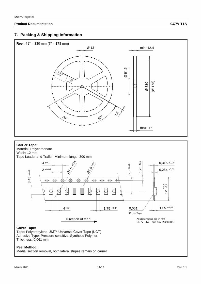
7. Packing & Shipping Information
Reel: 13” = 330 mm (7” = 178 mm)
max. 17
min. 12.4 Ø 13
(Ø 1
78
)
Carrier Tape: Material: Polycarbonate Width: 12 mm Tape Leader and Trailer: Minimum length 300 mm
2 ±0,05
4 ±0,1
3,4
5±
0,0
5
4 ±0,1
12
5,5
±0
,05
1,7
5±
0,1
0,254 ±0,02
1,75 ±0,05 0,061
Cover Tape
0,315 ±0,05+
0,3
-0
,1
All dimensions are in mm
CC7V-T1A_Tape-drw_20210311Direction of feed
1,05 ±0,05
Cover Tape: Tape: Polypropylene, 3M™ Universal Cover Tape (UCT) Adhesive Type: Pressure sensitive, Synthetic Polymer Thickness: 0.061 mm Peel Method: Medial section removal, both lateral stripes remain on carrier

Micro Crystal
Product Documentation CC7V-T1A
March 2021 12/12 Rev. 1.1
8. Compliance Information
Micro Crystal confirms that the standard product Quartz Crystal Unit CC7V-T1A is compliant with “EU RoHS Directive” and “EU REACh Directives”. Please find the actual Certificate of Conformance for Environmental Regulations on our website: CoC_Environment_CC&CM-Series.pdf
9. Document Revision History
Date Revision # Revision Details
March 2017 1.0 First release
March 2021 1.1
Adapted Application Examples, 2.1. Added package designation DFN-2, 5.4. Corrected Carrier Tape drawing, 7. Added new disclaimer
The information contained in this document is believed to be accurate and reliable. However, Micro Crystal assumes no responsibility for any consequences resulting from the use of such information nor for any infringement of patents or other rights of third parties, which may result from its use. In accordance with our policy of continuous development and improvement, Micro Crystal reserves the right to modify specifications mentioned in this publication without prior notice and as deemed necessary. Any use of Products for the manufacture of arms is prohibited. Customer shall impose that same obligation upon all third-party purchasers. Without the express written approval of Micro Crystal, Products are not authorized for use as components in safety and life supporting systems as well as in any implantable medical devices. The unauthorized use of Products in such systems / applications / equipment is solely at the risk of the customer and such customer agrees to defend and hold Micro Crystal harmless from and against any and all claims, suits, damages, cost, and expenses resulting from any unauthorized use of Products. No licenses to patents or other intellectual property rights of Micro Crystal are granted in connection with the sale of Micro Crystal products, neither expressly nor implicitly. In respect of the intended use of Micro Crystal products by customer, customer is solely responsible for observing existing patents and other intellectual property rights of third parties and for obtaining, as the case may be, the necessary licenses.
Micro Crystal AG Muehlestrasse 14 CH-2540 Grenchen Switzerland
Phone +41 32 655 82 82 [email protected] www.microcrystal.com