Procontrol P14 83SR51/R1210 Control Module for … · Control Module for Analog Control Functions...
30
Procontrol P14 83SR51R1210 Module and Application Description Control Module for Analog Control Functions with Continuous Output
Transcript of Procontrol P14 83SR51/R1210 Control Module for … · Control Module for Analog Control Functions...

Procontrol P14
83SR51R1210 Module and Application Description Control Module for Analog Control Functions with Continuous Output


Procontrol P14
83SR51R1210 Control Module for Analog Control Functions with Continuous Output

NOTICE This document contains information about one or more ABB products and may include a description of or a reference to one or more standards that may be generally relevant to the ABB products. The presence of any such description of a standard or reference to a standard is not a representation that all of the ABB products referenced in this document support all of the features of the described or referenced standard. In order to determine the specific features supported by a particular ABB product, the reader should consult the product specifications for the particular ABB product. ABB may have one or more patents or pending patent applications protecting the intellectual property in the ABB products described in this document. The information in this document is subject to change without notice and should not be construed as a commitment by ABB. ABB assumes no responsibility for any errors that may appear in this document. In no event shall ABB be liable for direct, indirect, special, incidental or consequential damages of any nature or kind arising from the use of this document, nor shall ABB be liable for incidental or consequential damages arising from use of any software or hardware described in this document. This document and parts thereof must not be reproduced or copied without written permission from ABB, and the contents thereof must not be imparted to a third party nor used for any unauthorized purpose. The software or hardware described in this document is furnished under a license and may be used, copied, or disclosed only in accordance with the terms of such license. This product meets the requirements specified in EMC Directive 2014/30/EC.
TRADEMARKS Procontrol is a registered trademark of ABB AG. All rights to copyrights, registered trademarks, and trademarks reside with their respective owners. Copyright © 2016 ABB. All rights reserved. Release: July 2016 Document number: 2VAA007465

TABLE OF CONTENTS
1. APPLICATION ................................................................................................. 8
2. FEATURES ...................................................................................................... 8
3. DESIGN OF THE MODULE ............................................................................. 9
3.1 Process Interface ............................................................................................... 9
3.2 Station-Bus Interface ......................................................................................... 9
3.3 Processing Section ........................................................................................... 9
4. STRUCTURING ............................................................................................. 10
5. ADRESSING .................................................................................................. 10
5.1 General ............................................................................................................. 10
5.2 Address Formation .......................................................................................... 10
5.3 Address List for Module Inputs ...................................................................... 10
5.4 Address List for Module Outputs ................................................................... 11
6. PARAMETER LIST ........................................................................................ 11
7. EVENT GENERATION .................................................................................. 11
8. SIMULATION ................................................................................................. 12
9. DISTURBANCE BIT EVALUATION, RECEIVE MONITORING .................... 12
10. DIAGNOSIS AND ANNUNCIATION FUNCTIONS ........................................ 12
10.1 Disturbance Annunciations on the Module ................................................... 12
10.2 Disturbance Annunciation Signals to the Annunciation System ................ 12
10.3 Diagnosis ......................................................................................................... 12
11. OPERATING STATES OF THE MODULE .................................................... 14
11.1 Initialization and Bootstrapping with User Lists ........................................... 14
11.2 Normal Operation ............................................................................................ 14
11.3 Changing the User Program ........................................................................... 14
11.4 Changing Fixed Values ................................................................................... 14
11.5 Changing Parameters ...................................................................................... 14
11.6 Simulation ........................................................................................................ 14

12. PROCESS INPUTS AND OUTPUTS ............................................................. 15
12.1 Output of Commands to the Process Interface ............................................ 15
12.2 Check Back Signals from the Process .......................................................... 15
13. CONFIGURATION OF INPUTS/OUTPUTS ................................................... 15
13.1 Setting of the system hum filter ..................................................................... 15
13.2 Setting of the analog inputs and outputs ...................................................... 15
13.3 Setting of the jumpers ..................................................................................... 15
14. MODULE CYCLE TIME ................................................................................. 15
15. APPLICATION OF FUNCTION BLOCKS ..................................................... 16
15.1 Overview ........................................................................................................... 16
16. FUNCTION DIAGRAM ................................................................................... 19
17. CONNECTION DIAGRAMS ........................................................................... 20
17.1 Connection diagram for an electrohydraulic or electropneumatic actuator (Process Interface 1) ....................................................................................... 20
17.2 Connection diagram for an electric motor - driven actuator (Process Interface 1) ....................................................................................................... 21
17.3 Connection diagram for an electrohydraulic or electropneumatic actuator (Process Interface 1) ....................................................................................... 22
17.4 Connection diagram for an electric motor - driven actuator (Process Interface 1) ....................................................................................................... 23
18. MODULE DESIGN ......................................................................................... 24
19. SYSTEM DATA .............................................................................................. 26
20. TECHNICAL DATA ........................................................................................ 26
20.1 Power supply ................................................................................................... 26
20.2 Process Interface ............................................................................................. 26
20.2.1 Input values .......................................................................................... 26
20.2.2 Output values ....................................................................................... 27
20.3 Analog signals ................................................................................................. 27
20.3.1 Input values .......................................................................................... 27

TABLE OF CONTENTS
20.3.2 Output values ....................................................................................... 27
20.3.3 Accuracy ............................................................................................... 28
20.3.4 Initialization time ................................................................................... 28
20.4 Interference immunity (of process inputs and outputs) ............................... 28
21. ORDERING DATA ......................................................................................... 28
22. REVISION HISTORY ..................................................................................... 29
Process Interface APPLICATION
1. APPLICATION The module is used for stored-program analog control on the drive control, group control and unit control levels. It is suitable for controlling the following actuators:
• Electrohydraulic actuators • Electropneumatic actuators • Electric motor-driven actuators
The positioning of the actuators takes place at the local transformer or, in the case of electric motor-driven actuators, in continuously operating power electronics system. In addition to the single-variable analog control functions, a super-ordinated master control function can be implemented. The module includes the function blocks needed for continuous single-variable control. For signal handling, further function blocks are available. The module is intended to be used with the Process Operator Station (POS30). The module uses 2 process interfaces for the power controllers and for the process.
2. FEATURES The module can be plugged into any station of the PROCONTROL bus system. It incorporates a standard interface for the PROCONTROL station bus. The module address is set automatically when the module is plugged into the PROCONTROL station. The telegrams received over the bus are checked by the module for error-free transmission based on their parity bits. The telegrams sent from the module to the bus are provided with parity bits, in order to ensure error-free transmission. The user program is stored on a nonvolatile memory (Flash–PROM). Loading and changing of the user program is done from the PDDS over the bus. The module is ready for operation as soon as a valid user program has been loaded. For communication with process and switchgear, the module requires the following voltages: USA/USB, branched internally into the following voltages:
• UK1 Supply for contacts, process interface 1 • UK2 Supply for contacts, process interface 2 • S11/S13 Supply for transducer, process interface 1 • S21/S23 Supply for transducer, process interface 2
The voltages are short-circuit-proof and non-interfering. The operating voltages and the external logic signals are related to reference conductor Z. In case the internal monitoring circuits or the input signal monitor respond, disturbance annunciation ST (general disturbance) will be indicated on the front panel of the module. Response of the internal monitoring circuits is indicated as disturbance annunciation SG (module disturbance) on the front panel of the module.
8 2VAA007465

DESIGN OF THE MODULE Process Interface
3. DESIGN OF THE MODULE The module essentially consists of:
• Process interfaces • Station-bus interface • Processing section
3.1 Process Interface In the process interfaces, the process signals are adapted to the signal levels.
3.2 Station-Bus Interface In the station-bus interface, the module signals are adapted to the bus. Mainly a parallel/serial conversion takes place. The module transfers the data telegrams through a standard interface to the station bus. Data transfer is serial.
3.3 Processing Section For processing the signals coming from the process and from the bus, the module is equipped with a microprocessor which cooperates with the following memory areas:
Contents Storage medium
Operating program Flash PROM
Function blocks Flash PROM
User program (structure, address and simulation list)
Flash PROM
History values RAM
Current module input and output signals (shared memory)
RAM
The operating program enables the microprocessor to perform the elementary operations of the module. The memory for the function blocks contains standard programs for implementing the different functions. All the function blocks, their inputs and outputs, can be called by the user via the Programming, Diagnosis and Display System (PDDS). The memory for the user program contains information on:
• how the function blocks are interconnected, • which module inputs and outputs are assigned to which inputs and outputs of the function blocks, • which fixed values are specified at the individual inputs of the function blocks, • which parameters are specified at the individual inputs of the function blocks, • which plant signals are assigned to which module inputs and outputs, • which function blocks support the process interfaces, • which function results, module input and output signals are simulated.
These information are defined by the user depending on the plant conditions. The entire user program is stored in a flash PROM. The settings (mainly for analog control) can be preset directly by the user at the respective function block inputs in the form of values (fixed values) or be specified as parameters. Fixed values and parameters can be modified at any time during operation (on-line). In this case they are changed and stored in the Flash PROM. The exchange of information between the module and the bus system takes place via the memory for the module's input and output signals (shared memory). This memory is used for buffering the signals.
2VAA007465 9

General STRUCTURING
4. STRUCTURING For structuring, the neutral inputs and outputs of the individual function blocks are assigned certain logic combinations. Inputs of function blocks can be connected to a module input, an output of another function block on the module (function results), or to fixed values and parameters. Outputs of function blocks can be logically combined with module outputs and function blocks on the module. For structuring, the following limit values of the module need to be taken into consideration:
• max. number of module inputs (EG) 510 • max. number of simulatable signals 32 • max. number of module outputs (AG) 255 • max. number of function results (AF) 255 • max. number of timers 256 • max. number of parameters 80 • max. number of lines in structure list 2886 • length of history value list (bytes) 2048 • dimensioning of the shared memory (cf. ”Addressing”)
A line is understood as one entry on the PDDS. For the precise procedure of structuring the function blocks please refer to the respective function block descriptions.
5. ADRESSING
5.1 General Signal exchange between the module and the bus system takes place via a shared memory. In this shared memory, incoming telegrams that the module is to receive and function results that are to leave the module are buffered. For this purpose, the shared memory includes send registers for telegrams to be sent and receive registers for telegrams to be received.
Dimensioning of the shared memory:
• Receive register: register numbers 0 - 254 • Send register: register numbers 0 - 199 • System register: register numbers 200 - 255
The allocations of the module's input and output signals to the registers of the shared memory are defined as specified by the user via the PDDS. The user data are contained in address lists.
5.2 Address Formation System address and station address are set at the station-bus coupling module or at the station-bus control module and are transferred by that module to all the modules of the relevant PROCONTROL station. The module addresses are defined through the connections on the backplane so that the modules are adjusted automatically when being plugged into a slot.
5.3 Address List for Module Inputs In the address list for module inputs, each module input is assigned the send-location address or the process interface of the signal to be received. In the case of module inputs which receive their signals over the bus, the addressing is effected by allocating the send-location address to EGn, e.g.:
10 2VAA007465

PARAMETER LIST Address List for Module Outputs
Input Address EG1 1, 32, 24, 8, 7 Bit no. (0 – 15) Register no. (0 – 255) Module no. (1 – 58) Station no. (1 – 249) System no. (0 – 3) In the case of module inputs that receive their signals from the Process Operator Station (POS30), addressing is done by allocating L,m to EGn, m being the register no. (0 - 199) of the module. This register number is no longer available for module outputs. For example: Input Address EG1 L,10
Destination telegram from the POS
The address list for inputs is translated by the PDDS into two internal lists, i.e. into the ”Bus address list” and the ”Module inputs allocation list”. The bus address list contains, for all telegrams to be used by the module, the send-location address and the receive register number. Incoming telegrams, whose addresses are contained in the bus address list, are registered in the receive register of the shared memory. The module ignores incoming telegrams, whose addresses are not part of the bus address list. The "Module inputs allocation list" contains for each module input the associated receive register number and, in the case of binary values, the bit position.
5.4 Address List for Module Outputs In the address list for module outputs, a send register is defined for each signal that is to leave the module and, in case of binary signals; a send bit is defined additionally, e.g.:
6. PARAMETER LIST The parameter list contains up to 80 parameters for function blocks. Parameter values can be changed on-line on the PDDS anytime.
7. EVENT GENERATION For each system cycle, the module is prompted once by the PROCONTROL system to send the information stored in the send registers of the shared memory. If values change within one cycle time, this will be treated as an event. The module recognizes the following conditions as an event:
• a change of the status in the case of binary values • a change of an analog value by a fixed threshold of 0.39 % and the expiration of a time-out of 200 msec after the
last transmission activity (cyclically or per event).
Function block EZS can be used to set these response values separately for each analog value (cf. Function block description). When an event occurs, the cyclic mode is interrupted, and the new values are given priority and transmitted over the bus.
Output Address
AG1 1, 5
Bit no.Register no.
(1 - 15)(0 - 199)
2VAA007465 11

Disturbance Annunciations on the Module SIMULATION
8. SIMULATION With the PDDS, a maximum of 32 module signals (function results, module inputs and outputs) can be overwritten with constant values (”simulated”). Simulation values can be changed on-line on the PDDS anytime. When a simulation is cancelled on the PDDS, a simulation data record is deleted and the module will go on operating with the data received from the bus or with the values formed inside the module.
9. DISTURBANCE BIT EVALUATION, RECEIVE MONITORING The telegrams received over the bus may be provided with a fault flag on bit position 0. This fault flag is generated by the sending module based on plausibility checks and is set to ”1” if certain disturbances occur (cf. the respective Module or Function Block Descriptions). In order to be able to detect errors occurring during signal transmission, the module is provided with a monitoring function for the cyclic renewal of the input telegrams. If a signal is not renewed for a certain amount of time (e.g. caused by a failure of the sending module), in the assigned receive register of the shared memory, the bit of position 0 will be set to ”1”. At the same time, in the case of binary value telegrams, all binary values will be set to ”0”. For analog values, the old value is maintained. A set disturbance bit does not automatically cause a reaction in the module. If the disturbance bit of a telegram is to be evaluated, this must be taken into consideration in the structuring process. Disturbance bits from telegrams received can be used inside the module only. They are not included in telegrams to be sent. Function blocks with processing functions for measured values do include disturbance bits in the telegrams to be sent. Further information on disturbance bit evaluation is given in the respective function block descriptions.
10. DIAGNOSIS AND ANNUNCIATION FUNCTIONS
10.1 Disturbance Annunciations on the Module On the module front, light-emitting diodes indicate the following conditions:
LED designation
• Disturbance ST • Module disturbance SG
The LED ST signals all disturbances of the module and disturbances in the data communication with the module. The LED SG signals module disturbances only.
10.2 Disturbance Annunciation Signals to the Annunciation System The annunciation system or the Control Diagnosis System CDS receives disturbance messages from the control module over the bus.
10.3 Diagnosis In the processing section of the module the received telegrams, the generation of the telegrams to be transmitted and the internal signal processing are monitored for errors (self-diagnosis). If a disturbance occurs, the type of the disturbance is stored in the diagnosis register and a disturbance signal is transmitted to the PROCONTROL system at the same time. When requested, the module transmits a telegram which contains the data stored in the diagnosis register (register 246) The contents of the diagnosis register, the signals on the general disturbance lines, the messages on the CDS, and lamps ST and SG are shown in Fig. 1. If message ”Process channel fault” is indicated in the diagnosis register, this may be due to the following causes:
• Short-circuit at outputs UK1, UK2, AF1, AF2, S11/S13 or S21/S23. • Analog input value not plausible, i.e. the values are lower than -6.25 % or higher than 150 %. • Wire break at analog outputs AY1 or AY2, in the case of a configuration for 4 ... 20 mA.
12 2VAA007465

DIAGNOSIS AND ANNUNCIATION FUNCTIONS Diagnosis
If message ”Processing fault” is indicated in the diagnosis register, this may be due to the following causes:
• Invalid structuring. • Relay driver for the analog inputs or outputs of function unit 1 (E11/E12, E13/E14, AY1)
or function unit 2 (E21/E22, E23/E24, AY2) defective. • Analog section for analog outputs AY1 or AY2 defective. • Disturbance of the internal module voltages. • Disturbance of the internal reference values of the analog inputs and outputs.
Figure 1: Diagnosis messages of 83SR51R1210 *) The Control Diagnosis System (CDS) provides a description for every message number. This description comprises:
• Information about cause and effect of the disturbance • Recommendations for elimination.
Thus, fast disturbance elimination is ensured
Bit 15 14 13 12 11 10 9 8 7 6 5 4 3 2 1 0
Type S S S S 0 S D S 0 0 0 S 0 S 0 0
Parameter fault Process channel fault Processing fault Checksum error detected
Timer defective Module restart executed Bus deactivation defective
Receive monitoring responded
Event mode fault
Wrong firmware PROM Hardware defect of processing section EEPROM not valid Processing initialization active
by bus control module Module address not within 1 - 58 Hardware defect of bus interface
Module not operating
Module not accessible from bus
Module operating Diagnosis register 246
6615 6600 6601 6602
6604 6605 6606
6610
6612
CDS messages *)
ST
SST ≥ 1 ≥ 1
D = Dynamic annunciations are cancelled after the contents of the diagnosis register has been transmitted S = Static annunciations disappear automatically upon deactivation
SG
SSG ≥ 1
0 = Not used
Module transmitter disconnected
2VAA007465 13

Initialization and Bootstrapping with User Lists OPERATING STATES OF THE MODULE
11. OPERATING STATES OF THE MODULE
11.1 Initialization and Bootstrapping with User Lists The initialization is effected either upon plugging-in of the module or after the voltage is connected. By initialization, the module is put into a defined initial state. During initialization, disturbance light-emitting diodes ST and SG are on. There is no user program available when the module is first started. The module signals ”Processing fault” and disturbance light-emitting diodes ST and SG are on. First, the user program of the PDDS has to be transmitted via bus into the RAM of the module. The procedure will start with the structure list, and the PDDS will call up the other lists automatically. The PDDS checks locations and addresses for each transmission activity in order to avoid wrong lists. The module checks each list received for plausibility. Now, the complete user program can be transferred per PDDS command into the Flash-PROM. After this procedure, the module is ready for operation and the disturbance light-emitting diodes ST and SG will go off.
11.2 Normal Operation The initialization is effected either upon plugging-in of the module or after the voltage is connected. By initialization, the module is put into a defined initial state. During initialization, disturbance light-emitting diodes ST and SG are on. There is no user program available when the module is first started. The module signals ”Processing fault” and disturbance light-emitting diodes ST and SG are on. First, the user program of the PDDS has to be transmitted via bus into the RAM of the module. The procedure will start with the structure list, and the PDDS will call up the other lists automatically. The PDDS checks locations and addresses for each transmission activity in order to avoid wrong lists. The module checks each list received for plausibility. Now, the complete user program can be transferred per PDDS command into the Flash-PROM. After this procedure, the module is ready for operation and the disturbance light-emitting diodes ST and SG will go off.
11.3 Changing the User Program User programs (structure, address, parameter and simulation list) can be transferred from the module into the PDDS or can be taken over from the data base. Changed user programs can be transferred back to the module. This may be done as described below:
• The changed user program is transferred by the PDDS into the RAM of the module. • Then, the module checks the user program in the background. If no faults are detected, the new list is activated
and transferred into the nonvolatile Flash-PROM.
When the new lists are activated, the old user program is compared to the new one. Only in the case of a discrepancy, an initialization phase will be carried out in the new user program. This means, all controllers and binary group control systems will enter ”Manual” mode, memory and timer elements are reset, and the commands present at the process interface are deactivated. In the case of changed addresses at module inputs (EGn), the respective shared-memory entries are set to zero until new data is received for the first time. If the lists are identical, the processing will not be interrupted by an initialization phase.
11.4 Changing Fixed Values Some fixed values in the structure list can be changed on-line via the PDDS. The changes made are stored in the Flash–PROM.
11.5 Changing Parameters Some parameters in the parameter list can be changed on-line via the PDDS. The changes made are stored in the Flash–PROM.
11.6 Simulation Via the PDDS, module signals can be specified and deleted. The simulation data is stored in the Flash-PROM.
14 2VAA007465

PROCESS INPUTS AND OUTPUTS Output of Commands to the Process Interface
12. PROCESS INPUTS AND OUTPUTS
12.1 Output of Commands to the Process Interface The output of setpoints to the process interface takes place at analog outputs AY1 and AY2, drive releases at binary outputs AF1 and AF2. Signal output to the process interface is effected via function block AP04 (output of analog and binary process signals).
12.2 Check Back Signals from the Process The checkback signals from the process can be connected to contact inputs STA1/2, TS1/2, EZ1/2, EO1/2 (cf. Connection diagrams). The supply of the contacts is provided via short-circuit-proof, monitored and non-interfering voltages UK1/2. Signal input from the process interface is via function block EP04 (input of analog and binary process signals).
13. CONFIGURATION OF INPUTS/OUTPUTS
13.1 Setting of the system hum filter The system hum filter is defined in the first EP04 function block for both analog inputs.
Indication PDDS
Input PDDS
Filtering
FIL 0 16 50 60
from 16 2/3 Hz
50 Hz standard setting 60 Hz
13.2 Setting of the analog inputs and outputs The configuration is defined by means of function blocks EP04 and AP04 (cf. Function block descriptions).
13.3 Setting of the jumpers Using jumpers X200 ... X203, the type of the analog-value transmitter connected to the analog input is set. X200 ... X203 mounted: Analog input n, grounded, for connecting 2-wire transducers fed from the module. X200 ... X203 mounted: Analog input n, non-grounded, for connecting 4-wire transducers fed from the module or
external sources.
14. MODULE CYCLE TIME A user program is run through with a fixed cycle time. The cycle time is defined in function block TXT2 at the beginning of the structure list. The module cycle time results from number and type of the function blocks listed in the structure list. The fixed cycle time in function block TXT2 is a time minimum. It applies if the time resulting from the processing of the structure list is shorter. The actual cycle time is stored in register 205 and can be read from the PDDS. In case the cycle time in register 205 exceeds the fixed module cycle time in the TXT2 function block, that time needs to be increased. On the module, cycle times of 20 msec up to 700 msec can be set in steps of 10 msec. For each module, the following scope of functions can be implemented at a cycle time of 50 msec:
• 2 drive control functions (ASP2)
In order to avoid major time errors in function blocks with time-value inputs, for time values of less than 10 sec only integer multiples of the module cycle time should be used.
2VAA007465 15

Overview APPLICATION OF FUNCTION BLOCKS
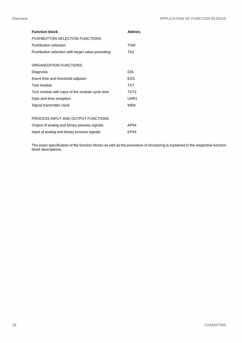
15. APPLICATION OF FUNCTION BLOCKS
15.1 Overview Function block Abbrev.
BINARY FUNCTIONS
Switch-off delay element ASV
2-out-of-3 selection, binary B23
2-out-of-4 selection, binary B24
M-out-of-N selection BMN
Bit marshalling BRA2
Dual-BCD-converter DBC1
Dual-decimal-converter DDC
Dynamic OR element DOD
Switch-on delay element ESV
Monostable flipflop, break MOA
Monostable flipflop, constant MOK
OR element ODR
RS flipflop RSR
AND element AND
Counter ZAE
BINARY GROUP CONTROL
Group control function for sequential control GSA2
Group control function for logic control GSV
Criteria call KRA1
Criteria call without time monitoring KRA3
Step function for multifunction SCH1
Preselection function, two-fold VW2
Preselection function, three-fold VW3
Preselection function, four-fold VW4
Selector switch, two-fold to four-fold WS41
DRIVE CONTROL
Drive control function, unidirectional drive ASE1
Drive control function, incremental output ASI2
Drive control function, solenoid valve ASM1
Drive control function, proportional output ASP2
Drive control function, actuator ASS1
Drive control function, reversible drive ASW
LIMIT-SIGNAL ELEMENTS
Limit signal for upper limit value GOG
Limit signal for lower limit value GUG
16 2VAA007465

APPLICATION OF FUNCTION BLOCKS Overview
Function block Abbrev.
ANALOG FUNCTIONS
Absolute value generator ABS
Limiter BEG
Divider DIV
Function generator FKG
Integrator INT1
Factor variation KVA
ANALOG FUNCTIONS
Maximum value selector MAX
Minimum value selector MIN
Multiplier MUL
Monitoring and selecting function MVN
Differentiator PDT
Dead-time element PT0
Delay element, 1st order PT1
Delay element, 2nd order PT2
Delay element, Nth order PTN
Square-root extractor RAD
Summing multiplier SMU
Time variation TVA
Change-over switch UMS
SIGNAL CONDITIONING FUNCTIONS
Enthalpy function ENT1
Correcting element for water level measurement NIV1
Non-linear filter FIL1
Correcting function, steam-flow measurement KOD
Correcting function, gas flow measurement KOG
Calculation of saturated-steam pressure SDD
Calculation of saturated-steam temperature SDT
ANALOG CONTROL
Auto/Manual station HST1
PID controller PID3
PI controller PIR3
P controller PRE
Differentiator with derivative-action time PTV
Setpoint integrator SWI1
Setpoint adjuster SWV1
Disturbance bit suppression SZU
2VAA007465 17
Overview APPLICATION OF FUNCTION BLOCKS
Function block Abbrev.
PUSHBUTTON SELECTION FUNCTIONS
Pushbutton selection TAW
Pushbutton selection with target value presetting TAZ
ORGANIZATION FUNCTIONS
Diagnosis DIA
Event time and threshold adjuster EZS
Text module TXT
Text module with input of the module cycle time TXT2
Date and time reception UHR1
Signal transmitter clock WEK
PROCESS INPUT AND OUTPUT FUNCTIONS
Output of analog and binary process signals AP04
Input of analog and binary process signals EP04
The exact specification of the function blocks as well as the procedure of structuring is explained in the respective function block descriptions.
18 2VAA007465

FUNCTION DIAGRAM Overview
16. FUNCTION DIAGRAM Terminal designations: The module consists of a printed circuit board (see “Module design”). The printed circuit board is equipped with connectors X21 and X11. Connector X21 contains all process inputs. Connector X11 incorporates the standard interface with the station bus and the operating voltages of the module.
* For proper functioning of the module, connector X11/d18 has to be connected to ZD (once per subrack)
+
UK1
X21
SGST
83SR
51-E
/R12
10
Stat
ion
bus
USA
ZZD
ZDZD
X11
d32
b32
b02
b14
d26
Z z32
Proc
ess
inte
rface
2
S11/
UK2
S21/
d18
z22
b24
z24
b22
b18
b20
AF2
UK2
STA2
TS2
EZ2
EO2
z18
z20
b28
AY2
Z21
S21
Mon
itorin
g
USB
d30
# =
# =
Pos.
setp
oint
Proc
ess
varia
ble
SRA
S23
S13
AF1
AF2
z28
S23
z30
z26
E24
E23
X203
z32
Z24
# =
b30
b26
E22
E21
X202
b32
Z22
Proc
ess
inte
rface
1
z06
b08
z08
b06
b02
b04
AF1
UK1
STA1
TS1
EZ1
EO1
z02
z04
b12
AY1
Z11
S11
# =
# =
Pos.
setp
oint
Proc
ess
varia
ble
z12
S13
z14
z10
E14
E13
X201
z16
Z14
# =
b14
b10
E12
E11
X200
b16
Z12
Para
llel/s
eria
lco
nver
sion
Shar
ed
mem
ory
Proc
esso
rO
pera
ting
prog
ram
Func
tion
bloc
ksR
AM
SS
Use
r fu
nctio
nsFl
ash
PRO
M
+
+
+
+
MU
su
pply
MU
su
pply
2VAA007465 19

Connection diagram for an electrohydraulic or electropneumatic actuator (Process Interface 1) CONNECTION DIAGRAMS
17. CONNECTION DIAGRAMS Each connection diagram can be applied to each channel.
17.1 Connection diagram for an electrohydraulic or electropneumatic actuator (Process Interface 1)
2-wire-transducer
83SR
51-E
/R12
10
Stat
ion
bus
Plan
t
SRA
ZDSS
Z
AY1
Z11
UK1
EZ1
EO1
USB
E11
S11
Anal
og in
put
e.g.
PO
S
USA
E
H2-
wire
trans
duce
r
X200
Ri
E13
S13
Anal
og in
put
any
proc
ess
varia
ble
2-w
iretra
nsdu
cer
X201
Ri
20 2VAA007465

CONNECTION DIAGRAMS Connection diagram for an electric motor - driven actuator (Process Interface 1)
17.2 Connection diagram for an electric motor - driven actuator (Process Interface 1)
2-wire transducer
83SR
51-E
/R12
10
Stat
ion
bus
Pow
er e
lect
roni
cs,
SRA
ZDSS
Z
AF1
AY1
Z11
STA1
UK1
EZ1
EO1
M
USB
TS1
cont
inuo
usly
USA
Plan
t
E11
S11
Anal
og in
put
e.g.
PO
S
2-w
iretra
nsdu
cer
X200
Ri
E13
S13
Anal
og in
put
any
proc
ess
varia
ble
2-w
iretra
nsdu
cer
X201
Ri
2VAA007465 21

Connection diagram for an electrohydraulic or electropneumatic actuator (Process Interface 1) CONNECTION DIAGRAMS
17.3 Connection diagram for an electrohydraulic or electropneumatic actuator (Process Interface 1)
4-wire transducer
83SR
51-E
/R12
10
Stat
ion
bus
Plan
t
SRA
ZDSS
Z
AY1
Z11
UK1
EZ1
EO1
USB
E11
Z12
Anal
og in
put
e.g.
PO
SUSA
E
H4-
wire
trans
duce
r
X200
Ri
Anal
og in
put
any
proc
ess
varia
ble
E12
S11
E13
Z14
4-w
iretra
nsdu
cer
X201
Ri
E14
S13
22 2VAA007465

CONNECTION DIAGRAMS Connection diagram for an electric motor - driven actuator (Process Interface 1)
17.4 Connection diagram for an electric motor - driven actuator (Process Interface 1)
4-wire transducerSt
atio
n bu
s
Pow
er e
lect
roni
cs,
SRA
ZDSS
Z
AF1
AY1
Z11
STA1
UK1
EZ1
EO1
M
USB
TS1
cont
inuo
usly
USA
Plan
t
83SR
51-E
/R12
10
E11
Z12
Anal
og in
put
e.g.
PO
S
4-w
iretra
nsdu
cer
X200
Ri
Anal
og in
put
any
proc
ess
varia
ble
E12
S11
E13
Z14
4-w
iretra
nsdu
cer
X201
Ri
E14
S13
2VAA007465 23

Connection diagram for an electric motor - driven actuator (Process Interface 1) MODULE DESIGN
18. MODULE DESIGN Board size: 6 units, 1 division, 160 mm deep Connector: acc. to DIN 41 612 / IEC 60603-2
1 x for station bus connection, 48-pole edge-connector, type F (connector X11) 1 x for process connection, 32-pole edge-connector, type F (connector X21)
Weight: approx. 0.55 kg View of connector side:
Contact assignments of process connector X21 View of contact side
b z
02 EZ1 AY1
04 EO1 Z11
06 TS1 AF1
08 UK1 STA1
10 E11 E13
12 S11 S13
14 E12 E14
16 Z12 Z14
18 EZ2 AY2
20 EO2 Z21
22 TS2 AF2
24 UK2 STA2
26 E21 E23
28 S21 S23
30 E22 E24
32 Z22 Z24
X 11
X 21
24 2VAA007465

MODULE DESIGN Connection diagram for an electric motor - driven actuator (Process Interface 1)
Side view and view of module front
83SR51
ST
X11
X21
ST
ABB
SG Disturbance
SG Module disturbance
X200
X201
X202
X203
ABB
2VAA007465 25

Power supply SYSTEM DATA
19. SYSTEM DATA Kind of influence Environmental Parameter Standard Characteristic/Value Operating conditions Climatic environment Ambient temperature IEC/EN 60068-2-2 0°C to +70°C, 16h
Relative humidity IEC/EN 60068-2-78 5% to 95% RH Atmospheric pressure IEC/EN 60068-1 86 kPa to 106 kPa
Electromagnetic compatibility (EMC)
Electrostatic discharge immunity IEC/EN 61000-4-2 Class 3 Class 2
Air discharge 8 kV Contact discharge 4 kV
Radiated, radio-frequency, electromagnetic field immunity
IEC/EN 61000-4-3 Class 3
80 MHz to 3000 MHz, 10 V/m, 80 % AM (1 kHz)
Electrical fast transient/burst immunity
- Supply lines for AC 120/230 V (burst)
- Supply lines for DC 24 V - Signal lines (I/O and bus lines)
IEC/EN 61000-4-4 Class 3
5/50 ns 2 kV 2 kV 2 kV
Surge immunity - Supply lines for AC 120/230 V
(burst) - Supply lines for DC 24 V - Signal lines (I/O and bus lines)
IEC/EN 61000-4-5 Class 4/3 Class 1/1 Class 3
1.2/50 ns 4/2 kV 0.5/0.5 kV 2 kV
Immunity to conducted disturbances, induced by radio-frequency fields
IEC/EN 61000-4-6 Class 3
0.15 MHz to 80 MHz, 10 V, 80% AM (1 kHz), Source impedance 150 Ω
Radiated emission CISPR16 / EN 55016 Class A
30 MHz to 1000 MHz, Limit Class A, group 1
Conditions of storage and transport Climatic environment Ambient temperature IEC/EN 60068-2-2 -40°C to +85°C, 16h
Relative humidity IEC/EN 60068-2-30 5% to 100% RH +25°C to 40°C (6 cycles)
Atmospheric pressure IEC/EN 60068-1 70 kPa to 106 kPa
20. TECHNICAL DATA
20.1 Power supply Operating voltage USA/USB 19.5 ... 30 V, typ. 24 V
Current consumption at USA/USB = 24 V 150 mA + output values
Power dissipation at USA/USB = 24 V 3.6 ... 8.4 W, depending on operating and signal status
Reference potential, process side Z = 0 V
Reference potential, bus side ZD = 0 V
binary signals
20.2 Process Interface
20.2.1 Input values Inputs EZn, EOn, TSn, STAn (n = 1, 2)
”0” signal 0 ... 3 V
”1” signal 11.2 ... 60 V
Input resistance 10 kOhm ± 5 %
Input current at UKn = 48 V 4.8 mA
Line resistance (supply and return line) ≤ 100 Ohm
Line length ≤ 1000 m
26 2VAA007465

TECHNICAL DATA Analog signals
20.2.2 Output values Contact voltages UKn (n = 1, 2)
Output voltage 48 V ± 10 %
Output current ≤ 30 mA
Response time of the monitoring function ≤ 1 s
The outputs are short-circuit-proof and non-interfering.
Drive release AFn (n = 1, 2)
Output voltage USA/USB - max. 4 V
Output current ≤ 100 mA
Line resistance (supply and return line) ≤ 50 Ohm
Line length ≤ 500 m
Response time of the monitoring ≤ 1 s
The outputs are short-circuit-proof and non-interfering.
20.3 Analog signals
20.3.1 Input values Inputs En1, En3 (n = 1, 2)
2-wire transducer,
jumpers X200, X201, X202 and X203 mounted
Input current, rated range (corresponding to 0 ... 100 %) 0/4 ... 20 mA
Maximum range -1 ... 50 mA
Input resistance (to Z) 50 Ohm
Line resistance (supply and return line) ≤ 50 Ohm
Line length ≤ 500 m
Response time of the monitoring function (at 4 ... 20 mA) ≤ 1 sec
Inputs En1/En2, En3/En4 (n = 1, 2)
4-wire transducer,
jumpers X200, X201, X202 and X203 not mounted
Input current, rated range (corresponding to 0 ... 100 %) 0/4 ... 20 mA
Maximum range -1 ... 50 mA
Input resistance (to En2 or En4) 50 Ohm
Line resistance (supply and return line) ≤ 50 Ohm
Line length ≤ 500 m
Response time of the monitoring function (at 4 ... 20 mA) ≤ 1 s
20.3.2 Output values Transducer supply Sn1, Sn3 (n = 1, 2)
Output voltage USA/USB - max. 4 V
Output current ≤ 50 mA
Line resistance (supply and return line) ≤ 50 Ohm
Line length ≤ 500 m
Response time of the monitoring function ≤ 1 s
2VAA007465 27

Interference immunity (of process inputs and outputs) ORDERING DATA
The outputs are short-circuit-proof and non-interfering. The outputs Sn1 and Sn3 are logically combined inside the module.
Analog outputs AYn/Zn1 (n = 1, 2)
Output current (impressed current) 0/4 ... 20 mA
Maximum output current 23 mA
Output voltage ≤ 13 V
Burden ≤ 500 Ohm
Line resistance (supply and return line) ≤ 50 Ohm
Line length ≤ 500 m
Response time of the monitoring function (at 4 ... 20 mA) ≤ 1 s
The outputs are short-circuit-proof, non-interfering and open-circuit-proof.
20.3.3 Accuracy For analog inputs and outputs
Accuracy, related to 100 % ≤ 0.5 %
Faults upon delivery ≤ 0.1 %
Quantization faults ≤ 0.02 %
Linearity faults ≤ 0.1 %
Temperature sensitivity ≤ 50 ppm/K (typ. 30 ppm/K)
Resolution 12 bits
Only for analog inputs
Common-mode rejection regarding potential Z 120 dB
Common-mode rejection at 16 2/3, 50 and 60 Hz 50 dB
20.3.4 Initialization time When the voltage is connected or the module plugged in 2 ... 22 s
20.4 Interference immunity (of process inputs and outputs) The product is in conformity with the provisions of the following European Directive: 2014/30/EC Directive of the European Parliament and of the Council of
26. Februar 2014 on the harmonization of the laws of member States relating to electromagnetic compatibility (EMC Directive)
Conformity to the stated Directive is assured through the application of the following harmonized standards:
Environment: Industry EMC, Emission: EN 61000-6-4: 2007/A1:2011 EMC, Immunity: EN 61000-6-2: 2005/AC:2005
See 2VAA002182R0301_CE-Conformity-P14.pdf for detailed technical data.
21. ORDERING DATA Order no. for complete module: Type designation: 83SR51R1210 Order number: GJR2396200R1210 Technical data are subject to change without notice!
28 2VAA007465

REVISION HISTORY Interference immunity (of process inputs and outputs)
22. REVISION HISTORY Rev. Date / Initial 1.0 Replaces 1 KGF 100 860 2016-07-12
CG
2VAA007465 29

ABB Inc. Power Generation Wickliffe, Ohio, USA E-Mail: [email protected] www.abb.com/controlsystems ABB AG Power Generation Mannheim, Germany E-Mail: [email protected] www.abb.com/controlsystems ABB Pte. Ltd. Power Generation Singapore E-Mail: [email protected] www.abb.com/controlsystems
Doc
umen
t Num
ber 2
VA
A00
7465
30 MD_2VAA007465_83SR51R1210.docx