Printed organic photodetectors for large area detection...
26
1 Printed organic photodetectors for large area detection on conformable substrates Jean-Marie VERILHAC [email protected] CEA Liten LCOI (Grenoble, France) (Printed Optoelectronic Components Laboratory)
Transcript of Printed organic photodetectors for large area detection...

1
Printed organic photodetectors for large area detection on
conformable substrates
Jean-Marie VERILHAC [email protected] CEA Liten LCOI (Grenoble, France) (Printed Optoelectronic Components Laboratory)

JM Verilhac_NDIP2014 2
Photodetecting devices
« Conventional » inorganic photodetectors Organic photodetectors
Phototransistors K.S. Karayan et al, Appl. Phys. Lett. 79, 1891 (2001)
Photoresistors D. Natali et al, Proceedings of ESSDERC 2002, Firenze, 2002, 523-526
CCD C.P. Watson et al, Appl. Phys. Lett. 99, 223304 (2011)
Photodiodes G. Yu et al, Science 270, 1789 (1995)
(1)
(2)
(4)
(5)
(1) Photomultiplier tubes (2) Si photodiode (p-n; p-i-n) (3) Phototransistor (4) Pyroelectric photodetector (5) Photoresistor (6) Charge-Coupled Device (CCD) (7) Bolometer
(3)
(6) (7)

Ease for large surface integration, Use of flexible plastic substrates, Compatibility with high throughput
printing tools, Short development cycles, Well adapted for non standard designs, Ease of hybridization on existing
technologies,
3
Organic vs inorganic: complementary technologies
Organic Inorganic
High performances, Robust and reliable devices, Well established technologies and
industrial context,
Lower performances (still under improvement),
Industrial field under construction.
Needs for cost effective tools, Long development cycles, Low versatility (difficulties for exotic
integration).
but…
but…
JM Verilhac_NDIP2014

4
Unique properties: Electrical properties of semiconductors and conductors (if doped), High absorption coefficients of organic materials, Mechanical properties of polymers, Ease of process of polymers.
π-conjugated organic materials
Benzene Polyparaphenylene vinylene Ethylene
JM Verilhac_NDIP2014
Chem. Commun., p578 (1977)
5
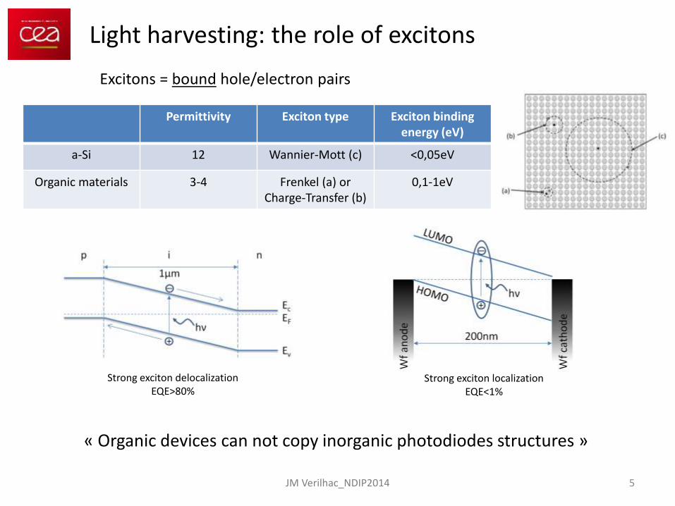
Light harvesting: the role of excitons
Excitons = bound hole/electron pairs
Permittivity Exciton type Exciton binding energy (eV)
a-Si 12 Wannier-Mott (c) <0,05eV
Organic materials 3-4 Frenkel (a) or Charge-Transfer (b)
0,1-1eV
Strong exciton delocalization EQE>80%
Strong exciton localization EQE<1%
« Organic devices can not copy inorganic photodiodes structures »
JM Verilhac_NDIP2014

6
1. Light Absorption - ηabs 2. Exciton Diffusion- ηED
3. Exciton Dissociation - ηCT 4. Charge Collection- ηCC
ηEQE= ηabs ηED ηCT ηCC
C.W. Tang, Appl. Phys. Lett. 1985, 48, 183
hν
+
-
X X
X
Combination of Donor and Acceptor material
JM Verilhac_NDIP2014

7
Planar heterojunction vs bulk heterojunction
Typical exciton diffusion length in conjugated polymers: Ld~10nm (Optimum domains length ~2Ld)
Top electrode
Bottom electrode
Top electrode
Bottom electrode
Acceptor Donor
Bilayer heterojunction Poorly efficient devices
EQE~1%
Bulk heterojunction Highly efficient devices
EQE~50-100%
20nm
10
0-2
00
nm
Donor
Acceptor
R.H. Friend et al., Nature 1995, 376, 498 A.J. Heeger et al., Science 1995, 270, 1789
JM Verilhac_NDIP2014

8
Visualisation of the bulk heterojunction
A.J. Heeger et al., Nano Lett. 2009, 9, 230
Transmission Electron Microscopy (TEM)
JM Verilhac_NDIP2014

9
Quantum Efficiency (1/2)
A.J. Heeger et al, Nat. Photonics 3 (2009), 297
P0 incident light Pabs absorbed light
JM Verilhac_NDIP2014

10 Y. Kim et al., Nat. Mater., 2006, 5, 197
S
S
S
n
S
S
S
n
Regioregular P3HT
Amorphous P3HT
Solid lines: without annealing Dashed lines: with annealing
Quantum Efficiency (2/2)
“Major impact of materials and blend morphology”
JM Verilhac_NDIP2014
B. Ray et al., Sol. Energ. Mat. Sol. C., 2012, 99, 204

-5 -4 -3 -2 -1 0 1 210
-10
10-9
10-8
10-7
10-6
10-5
10-4
10-3
10-2
Curr
ent density (
A/c
m²)
Voltage (V)
illumination
dark
11
Reverse dark current
Topological defects (pinholes, spikes, dusts), Injection from electrodes: barrier height, Gap states (thermal generation, tunneling current), Unintentional doping, Morphology (material percolation), Ground state charge transfer.
Charge generation through gap states Defects (scratch) revaled by Dark Lock In Thermography
JM Verilhac_NDIP2014

Reverse dark current: impact of contact barrier height
12 JM Verilhac_NDIP2014 J.M. Verilhac et al., Adv. Mater. 2013, 25, 6534

13
Photocurrent linearity
Others figures of merit
Response time
Low light intensity Photocurrent mainly limited by traps,
High light intensity photocurrent limited by Langevin recombination.
J. Huang et al., Chapter6, Organic Electronics in Sensors and biotechnology
Organic slower than Si Rooms for optimizations
Ref Si photodiode~50ns
10-6
10-5
10-4
10-3
10-2
10-1
10-10
10-9
10-8
10-7
10-6
10-5
10-4
10-3
Ph
oto
cu
rre
nt
(A)
Light Intensity (lumens)
Data taken from Benjamin Bouthinon PhD (CEA/IMEP)
JM Verilhac_NDIP2014

14
Mechanical strain: organic vs inorganic photodiodes on plastic substrate
a-Si:H photodiode Organic photodiode
“Failure limits of organic photodiodes exceed those of a-Si:H under tension and compression strains”
T.N Ng et al., Adv. Mater. 2009, 21, 1855
Min radius of curvature under Organic PD a-Si:H PD
Tension 7,5mm 20mm
Compression <2,5mm 12,5mm
JM Verilhac_NDIP2014

15
Organic layer for photoconversion
Vacuum evaporation (small molecules)
Solution-process (small molecules/polymers)
« Infinity of solutions offered by organic chemical synthesis and chemical designs »
JM Verilhac_NDIP2014

16
Donors polymers: Band Gap tuning
1st strategy: Planarizing the polymer backbone
2nd strategy: Push-Pull: combination of electron-
deficient and electron-rich units
Gap~2eV
Gap~1eV
E.W. Meijer et al. Mater. Sci. Eng. R., 2001, 32, 1 JM Verilhac_NDIP2014
17
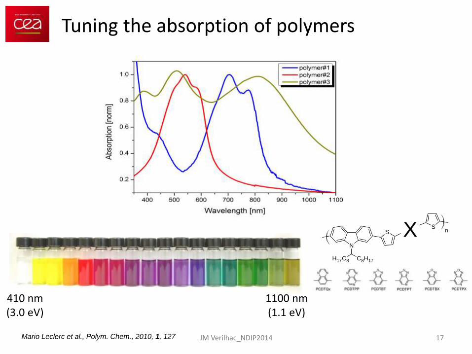
Tuning the absorption of polymers
410 nm (3.0 eV)
1100 nm (1.1 eV)
Mario Leclerc et al., Polym. Chem., 2010, 1, 127
N
C8H17H17C8
S X Sn
JM Verilhac_NDIP2014

18
Photodetection in the near-infrared
JM Verilhac_NDIP2014
400 600 800 1000 12000
10
20
30
40
50
60
70
Exte
rna
l Q
ua
ntu
m E
ffic
iency (
%)
Wavelength (nm)
Photoconversion layer A
Photoconversion layer B
Photoconversion layer C
Max light harvesting near 1100nm, due to currently available materials.
Polymer (tunable band gap)
Acceptor molecule (« almost frozen »)
LUMO
LUMO
Op
tica
l gap
HOMO
HOMO
Driving force for charge separation

19
Acceptors: Fulleren derivatives
Good solubility, Good electron mobility, Low lying LUMO (well matched with
conventional polymeric semiconductors), Good miscibility with polymers, Low absorption in the visible. [60]PCBM
Examples of some fulleren derivatives
Bis-[60]PCBM Tris-[60]PCBM
Bis-indene
[70]PCBM
“Current best material choice for organic bulk-heterojunction systems”
1nm H.W. Kroto et al., Nature 1985, 318, 162
JM Verilhac_NDIP2014

20
Printing: « the » disruptive technology?
Graphic art printing techniques well adapted for organic macroelectronic: ► Thicknesses of printed layer<100nm, ► Good layer homogeneity, ► Micrometric resolution and alignment, ► Sheet to sheet or roll to roll.
(1)
(2)
(3)
(4)
(5) (6)
(7)
(1) Screen-printing
(2) Inkjet (3) Spray-coating
(4) Slot-die
(5) Inkjet (lab tool) (6) Local spray coating (7) Gravure printing
Images taken from CEA JM Verilhac_NDIP2014

21
Some challenges about printing
with « Almost » without
Edge effect (coffee stain) Wetting
Resolutions (line/space)
γsubstrate > γink
400µm
Decreasing spacing
Inks formulation
JM Verilhac_NDIP2014

22
Printed OPD devices on large area (Gen1)
Fully printed OPD devices (>1000/sheet) Custom printed OPD designs
Image from CEA/ISORG Image from CEA/ISORG
380mm
32
0m
m
JM Verilhac_NDIP2014

23
Organic photodetectors on Active matrix
JM Verilhac_NDIP2014
Fully solution-processed and flexible visible imager (OTFT + OPD),
Collaboration between CEA/ISORG/plastic Logic (Flexi Award 2014),
Demo substrate size: 50x50mm, 96x96 pixels, Pixel size = 175µm, Pixels spacing = 200µm (<30µm for next demo), Process compatible with large area.

24 OP
D d
ata
shee
t
21 employees, Technological developments supported by
CEA, Manufacturing plants by mid 2016, Customized discrete OPD and imager
designs on large area, rigid and flexible substrates,
Fields of applications: medical, industrial, scientific, security, consumer…
Contact: [email protected] Website: www.isorg.fr
JM Verilhac_NDIP2014
ISORG (Image Sensor ORGanic)

25
Conclusions
JM Verilhac_NDIP2014
Organic photodetectors have gained in maturity in the last ten years, and are now on the way to be commercialized,
Organic photodetectors take unique advantages of organic materials (opto-electronic properties and processability),
Photoconversion from UV up to the near infrared,
Organic photodetectors are compatible with large area and flexible substrates, and could be hybridized on many existing inorganic technologies.

26
Thank you for your attention
JM Verilhac_NDIP2014