
PRINCIPLES OF POWER INTEGRITY FOR PDN DESIGN...
72
P RINCIPLES OF P OWER I NTEGRITY FOR PDN D ESIGN — S IMPLIFIED
Transcript of PRINCIPLES OF POWER INTEGRITY FOR PDN DESIGN...

PRINCIPLES OF POWER INTEGRITY FOR PDN DESIGN—SIMPLIFIED
9780132735551_print.indb i9780132735551_print.indb i 23/02/17 9:07 PM23/02/17 9:07 PM

9780132735551_print.indb ii9780132735551_print.indb ii 23/02/17 9:07 PM23/02/17 9:07 PM
PRINCIPLES OF POWER INTEGRITY FOR PDN DESIGN—SIMPLIFIEDR O B U S T A N D C O S T
E F F E C T I V E D E S I G N F O R H I G H S P E E D D I G I TA L P R O D U C T S
Larry D. Smith
Eric Bogatin
Boston • Columbus • Indianapolis • New York • San Francisco • Amsterdam Cape Town • Dubai • London • Madrid • Milan • Munich • Paris • Montreal
Toronto • Delhi • Mexico City • São Paulo • Sydney • Hong Kong • Seoul Singapore • Taipei • Tokyo
9780132735551_print.indb iii9780132735551_print.indb iii 23/02/17 9:07 PM23/02/17 9:07 PM

Many of the designations used by manufacturers and sellers to distinguish their products are claimed as trademarks. Where those designations appear in this book, and the publisher was aware of a trademark claim, the designations have been printed with initial capital letters or in all capitals.
The authors and publisher have taken care in the preparation of this book, but make no expressed or implied warranty of any kind and assume no responsibility for errors or omissions. No liability is assumed for incidental or consequential damages in connection with or arising out of the use of the information or programs contained herein.
For information about buying this title in bulk quantities, or for special sales opportunities (which may include electronic versions; custom cover designs; and content particular to your business, training goals, marketing focus, or branding interests), please contact our corporate sales department at [email protected] or (800) 382-3419.
For government sales inquiries, please contact [email protected].
For questions about sales outside the U.S., please contact [email protected].
Visit us on the Web: informit.com/aw
Library of Congress Control Number: 2017930426
Copyright © 2017 Pearson Education, Inc.
All rights reserved. Printed in the United States of America. This publication is protected by copyright, and permission must be obtained from the publisher prior to any prohibited reproduction, storage in a retrieval system, or transmission in any form or by any means, electronic, mechanical, photocopying, recording, or likewise. For information regarding permissions, request forms and the appropriate contacts within the Pearson Education Global Rights & Permissions Department, please visit www.pearsoned.com/permissions/.
ISBN-13: 978-0-13-273555-1ISBN-10: 0-13-273555-5
1 17
PublisherMark Taub
Editor-in-ChiefGreg Wiegand
Acquisitions EditorKim Boedigheimer
Managing EditorSandra Schroeder
Senior Project EditorLori Lyons
Production ManagerDhayanidhi
CopyeditorPaula Lowell
IndexerErika Millen
ProofreaderSam Sunder Singh
Editorial AssistantOlivia Basegio
Cover CompositorChuti Prasertsith
CompositorcodeMantra
9780132735551_print.indb iv9780132735551_print.indb iv 23/02/17 9:07 PM23/02/17 9:07 PM

The creation of this book took more than the 5,000 person-hours of writing, simulating, and editing and more than 500 hours of
conference calls. We could not have done this without the unfailing support and confi dence from our wives, Susan and
Marty, who kept the faith and gave us encouragement even during the long hours of writing, rewriting, and more rewriting.
Larry would also like to dedicate this book to his father, who was his undergrad Professor of Electrical Engineering.
9780132735551_print.indb v9780132735551_print.indb v 23/02/17 9:07 PM23/02/17 9:07 PM

9780132735551_print.indb vi9780132735551_print.indb vi 23/02/17 9:07 PM23/02/17 9:07 PM
vii
C O N T E N T S A T A G L A N C E
Preface .................................................................................................................. xix
Acknowledgments ................................................................................................ xxvii
About the Authors ................................................................................................ xxix
Chapter 1 Engineering the Power Delivery Network .............................................1
Chapter 2 Essential Principles of Impedance for PDN Design ............................ 17
Chapter 3 Measuring Low Impedance ................................................................ 69
Chapter 4 Inductance and PDN Design ............................................................ 137
Chapter 5 Practical Multi-Layer Ceramic Chip Capacitor Integration .............. 205
Chapter 6 Properties of Planes and Capacitors ................................................. 275
Chapter 7 Taming Signal Integrity Problems When Signals Change Return Planes ...................................................................... 363
Chapter 8 The PDN Ecology ............................................................................ 427
Chapter 9 Transient Currents and PDN Voltage Noise ..................................... 547
Chapter 10 Putting It All Together: A Practical Approach to PDN Design ........ 643
Index .................................................................................................................... 761
9780132735551_print.indb vii9780132735551_print.indb vii 23/02/17 9:07 PM23/02/17 9:07 PM

9780132735551_print.indb viii9780132735551_print.indb viii 23/02/17 9:07 PM23/02/17 9:07 PM
ix
C O N T E N T S
Preface .................................................................................................................. xix
Acknowledgments ................................................................................................ xxvii
About the Authors ................................................................................................ xxix
Chapter 1 Engineering the Power Delivery Network ...............................................1
1.1 What Is the Power Delivery Network (PDN) and Why Should I Care? ...............................................................1
1.2 Engineering the PDN ...................................................................5
1.3 “Working” or “Robust” PDN Design ...........................................8
1.4 Sculpting the PDN Impedance Profi le ........................................ 12
1.5 The Bottom Line ........................................................................ 14
Reference .................................................................................... 15
Chapter 2 Essential Principles of Impedance for PDN Design .............................. 17
2.1 Why Do We Care About Impedance? ......................................... 17
2.2 Impedance in the Frequency Domain ......................................... 18
2.3 Calculating or Simulating Impedance ......................................... 21
2.4 Real Circuit Components vs. Ideal Circuit Elements .................. 26
2.5 The Series RLC Circuit ............................................................... 30
2.6 The Parallel RLC Circuit ............................................................ 34
9780132735551_print.indb ix9780132735551_print.indb ix 23/02/17 9:07 PM23/02/17 9:07 PM
x Contents
2.7 The Resonant Properties of a Series and Parallel RLC Circuit ............................................................................36
2.8 Examples of RLC Circuits and Real Capacitors ......................42
2.9 The PDN as Viewed by the Chip or by the Board ....................46
2.10 Transient Response ..................................................................52
2.11 Advanced Topic: The Impedance Matrix .................................56
2.12 The Bottom Line .....................................................................66
References ................................................................................68
Chapter 3 Measuring Low Impedance ...............................................................69
3.1 Why Do We Care About Measuring Low Impedance? ............69
3.2 Measurements Based on the V/I Defi nition of Impedance .......70
3.3 Measuring Impedance Based on the Refl ection of Signals ......71
3.4 Measuring Impedance with a VNA .........................................76
3.5 Example: Measuring the Impedance of Two Leads in a DIP ...................................................................................81
3.6 Example: Measuring the Impedance of a Small Wire Loop .....86
3.7 Limitations of VNA Impedance Measurements at Low Frequency ....................................................................89
3.8 The Four-Point Kelvin Resistance Measurement Technique ....93
3.9 The Two-Port Low Impedance Measurement Technique .........95
3.10 Example: Measuring the Impedance of a 1-inch Diameter Copper Loop ...............................................................102
3.11 Accounting for Fixture Artifacts ...........................................105
3.12 Example: Measured Inductance of a Via ...............................109
3.13 Example: Small MLCC Capacitor on a Board ......................114
3.14 Advanced Topic: Measuring On-Die Capacitance .................120
3.15 The Bottom Line ...................................................................134
References ..............................................................................136
Chapter 4 Inductance and PDN Design ...........................................................137
4.1 Why Do We Care About Inductance in PDN Design? ...........137
4.2 A Brief Review of Capacitance to Put Inductance in Perspective .........................................................................138
9780132735551_print.indb x9780132735551_print.indb x 23/02/17 9:07 PM23/02/17 9:07 PM

xi
4.3 What Is Inductance? Essential Principles of Magnetic Fields and Inductance ............................................141
4.4 Impedance of an Inductor .....................................................147
4.5 The Quasi-Static Approximation for Inductance ..................150
4.6 Magnetic Field Density, B .....................................................155
4.7 Inductance and Energy in the Magnetic Field .......................159
4.8 Maxwell’s Equations and Loop Inductance ...........................163
4.9 Internal and External Inductance and Skin Depth ................167
4.10 Loop and Partial, Self- and Mutual Inductance ....................172
4.11 Uniform Round Conductors ..................................................175
4.12 Approximations for the Loop Inductance of Round Loops .........................................................................179
4.13 Loop Inductance of Wide Conductors Close Together ..........182
4.14 Approximations for the Loop Inductance of Any Uniform Transmission Line .......................................188
4.15 A Simple Rule of Thumb for Loop Inductance .....................194
4.16 Advanced Topic: Extracting Loop Inductance from the S-parameters Calculated with a 3D Field Solver .....195
4.17 The Bottom Line ...................................................................202
References ..............................................................................204
Chapter 5 Practical Multi-Layer Ceramic Chip Capacitor Integration ............205
5.1 Why Use Capacitors? .............................................................205
5.2 Equivalent Circuit Models for Real Capacitors .....................206
5.3 Combining Multiple Identical Capacitors in Parallel .............209
5.4 The Parallel Resonance Frequency Between Two Different Capacitors .......................................................211
5.5 The Peak Impedance at the PRF ...........................................215
5.6 Engineering the Capacitance of a Capacitor ..........................220
5.7 Capacitor Temperature and Voltage Stability ........................222
5.8 How Much Capacitance Is Enough? ......................................225
5.9 The ESR of Real Capacitors: First- and Second-Order Models ...................................................................................229
Contents xi
9780132735551_print.indb xi9780132735551_print.indb xi 23/02/17 9:07 PM23/02/17 9:07 PM
5.10 Estimating the ESR of Capacitors from Spec Sheets .............234
5.11 Controlled ESR Capacitors ...................................................238
5.12 Mounting Inductance of a Capacitor ....................................240
5.13 Using Vendor-Supplied S-parameter Capacitor Models ........251
5.14 How to Analyze Vendor-Supplied S-Parameter Models ........254
5.15 Advanced Topics: A Higher Bandwidth Capacitor Model .....258
5.16 The Bottom Line ...................................................................272
References ..............................................................................274
Chapter 6 Properties of Planes and Capacitors ...............................................275
6.1 The Key Role of Planes .........................................................275
6.2 Low-Frequency Property of Planes: Parallel Plate Capacitance ...........................................................................278
6.3 Low-Frequency Property of Planes: Fringe Field Capacitance ..................................................................279
6.4 Low-Frequency Property of Planes: Fringe Field Capacitance in Power Puddles ...............................................285
6.5 Loop Inductance of Long, Narrow Cavities ..........................290
6.6 Spreading Inductance in Wide Cavities ..................................292
6.7 Extracting Spreading Inductance from a 3D Field Solver ......304
6.8 Lumped-Circuit Series and Parallel Self-Resonant Frequency ..............................................................................307
6.9 Exploring the Features of the Series LC Resonance ..............312
6.10 Spreading Inductance and Source Contact Location .............315
6.11 Spreading Inductance Between Two Contact Points ..............317
6.12 The Interactions of a Capacitor and Cavities.........................325
6.13 The Role of Spreading Inductance: When Does Capacitor Location Matter? ...................................................................327
6.14 Saturating the Spreading Inductance .....................................332
6.15 Cavity Modal Resonances and Transmission Line Properties ......................................................................334
6.16 Input Impedance of a Transmission Line and Modal Resonances ............................................................................340
xii Contents
9780132735551_print.indb xii9780132735551_print.indb xii 23/02/17 9:07 PM23/02/17 9:07 PM

xiii
6.17 Modal Resonances and Attenuation ......................................343
6.18 Cavity Modes in Two Dimensions .........................................347
6.19 Advanced Topic: Using Transfer Impedance to Probe Spreading Inductance ..............................................354
6.20 The Bottom Line ...................................................................361
References ..............................................................................362
Chapter 7 Taming Signal Integrity Problems When Signals Change Return Planes ....................................................................363
7.1 Signal Integrity and Planes ....................................................363
7.2 Why the Peak Impedances Matter .........................................364
7.3 Reducing Cavity Noise through Lower Impedance and Higher Damping .............................................................367
7.4 Suppressing Cavity Resonances with Shorting Vias ...............372
7.5 Suppressing Cavity Resonances with Many DC Blocking Capacitors ........................................................... 383
7.6 Estimating the Number of DC Blocking Capacitors to Suppress Cavity Resonances ..............................................387
7.7 Determining How Many DC Blocking Capacitors Are Needed to Carry Return Current ...........................................393
7.8 Cavity Impedance with a Suboptimal Number of DC Blocking Capacitors ...................................................397
7.9 Spreading Inductance and Capacitor Mounting Inductance .............................................................................401
7.10 Using Damping to Suppress Parallel Resonant Peaks Created by a Few Capacitors .......................................403
7.11 Cavity Losses and Impedance Peak Reduction ......................408
7.12 Using Multiple Capacitor Values to Suppress Impedance Peak.....................................................................411
7.13 Using Controlled ESR Capacitors to Reduce Peak Impedance Heights ................................................................414
7.14 Summary of the Most Important Design Principles for Managing Return Planes ..................................................418
Contents xiii
9780132735551_print.indb xiii9780132735551_print.indb xiii 23/02/17 9:07 PM23/02/17 9:07 PM
7.15 Advanced Topic: Modeling Planes with Transmission Line Circuits ....................................................419
7.16 The Bottom Line ...................................................................423
References ..............................................................................425
Chapter 8 The PDN Ecology ..........................................................................427
8.1 Putting the Elements Together: The PDN Ecology and the Frequency Domain ...................................................428
8.2 At the High-Frequency End: The On-Die Decoupling Capacitance ...........................................................................430
8.3 The Package PDN .................................................................440
8.4 The Bandini Mountain ..........................................................447
8.5 Estimating the Typical Bandini Mountain Frequency ............452
8.6 Intrinsic Damping of the Bandini Mountain .........................456
8.7 The Power Ground Planes with Multiple Via Pair Contacts ...................................................................460
8.8 Looking from the Chip Through the Package into the PCB Cavity ...............................................................465
8.9 Role of the Cavity: Small Boards, Large Boards, and “Power Puddles” .............................................................469
8.10 At the Low Frequency: The VRM and Its Bulk Capacitor ......................................................................476
8.11 Bulk Capacitors: How Much Capacitance Is Enough? ..........479
8.12 Optimizing the Bulk Capacitor and VRM .............................483
8.13 Building the PDN Ecosystem: The VRM, Bulk Capacitor, Cavity, Package, and On-Die Capacitance ............488
8.14 The Fundamental Limits to the Peak Impedance ..................492
8.15 Using One Value MLCC Capacitor on the Board-General Features .........................................................498
8.16 Optimizing the Single MLCC Capacitance Value ..................502
8.17 Using Three Different Values of MLCC Capacitors on the Board ........................................................507
8.18 Optimizing the Values of Three Capacitors ...........................511
xiv Contents
9780132735551_print.indb xiv9780132735551_print.indb xiv 23/02/17 9:07 PM23/02/17 9:07 PM

xv
8.19 The Frequency Domain Target Impedance Method (FDTIM) for Selecting Capacitor Values and the Minimum Number of Capacitors ....................................514
8.20 Selecting Capacitor Values with the FDTIM .........................516
8.21 When the On-Die Capacitance Is Large and Package Lead Inductance Is Small ...............................................................521
8.22 An Alternative Decoupling Strategy Using Controlled ESR Capacitors ...................................................527
8.23 On-Package Decoupling (OPD) Capacitors ...........................532
8.24 Advanced Section: Impact of Multiple Chips on the Board Sharing the Same Rail .................................................540
8.25 The Bottom Line ...................................................................543
References ......................................................................................545
Chapter 9 Transient Currents and PDN Voltage Noise ....................................547
9.1 What’s So Important About the Transient Current? ..............547
9.2 A Flat Impedance Profi le, a Transient Current, and a Target Impedance ..................................................................550
9.3 Estimating the Transient Current to Calculate the Target Impedance with a Flat Impedance Profi le ..............................552
9.4 The Actual PDN Current Profi le Through a Die ...................553
9.5 Clock-Edge Current When Capacitance Is Referenced to Both Vss and Vdd..............................................................558
9.6 Measurement Example: Embedded Controller Processor ......562
9.7 The Real Origin of PDN Noise—How Clock-Edge Current Drives PDN Noise ....................................................565
9.8 Equations That Govern a PDN Impedance Peak ..................572
9.9 The Most Important Current Waveforms That Characterize the PDN ...........................................................577
9.10 PDN Response to an Impulse of Dynamic Current ...............579
9.11 PDN Response to a Step Change in Dynamic Current ..........582
9.12 PDN Response to a Square Wave of Dynamic Current at Resonance ..........................................................................585
Contents xv
9780132735551_print.indb xv9780132735551_print.indb xv 23/02/17 9:07 PM23/02/17 9:07 PM

9.13 Target Impedance and the Transient and AC Steady-State Responses ...................................................589
9.14 Impact of Reactive Elements, q-Factor, and Peak Impedances on PDN Voltage Noise .......................................595
9.15 Rogue Waves ..........................................................................602
9.16 A Robust Design Strategy in the Presence of Rogue Waves ...610
9.17 Clock-Edge Current Impulses from Switched Capacitor Loads ....................................................................613
9.18 Transient Current Waveforms Composed of a Series of Clock Impulses .....................................................622
9.19 Advanced Section: Applying Clock Gating, Clock Swallowing, and Power Gating to Real CMOS Situations .....629
9.20 Advanced Section: Power Gating ...........................................633
9.21 The Bottom Line ...................................................................638
References ..............................................................................640
Chapter 10 Putting It All Together: A Practical Approach to PDN Design ...............................................................................643
10.1 Reiterating Our Goal in PDN Design ....................................643
10.2 Summary of the Most Important Power Integrity Principles ................................................................645
10.3 Introducing a Spreadsheet to Explore Design Space ..............654
10.4 Lines 1–12: PDN Input Voltage, Current, and Target Impedance Parameters ...........................................................658
10.5 Lines 13–24: 0th Dip (Clock-Edge) Noise and On-Die Parameters .............................................................................661
10.6 Extracting the Mounting Inductance and Resistance .............665
10.7 Analyzing Typical Board and Package Geometries for Inductance .......................................................................674
10.8 The Three Loops of the PDN Resonance Calculator (PRC) Spreadsheet .................................................................677
10.9 The Performance Figures of Merit ........................................682
10.10 Signifi cance of Damping and q-factors ...............................685
xvi Contents
9780132735551_print.indb xvi9780132735551_print.indb xvi 23/02/17 9:07 PM23/02/17 9:07 PM

xvii
10.11 Using a Switched Capacitor Load Model to Stimulate the PDN ..............................................................694
10.12 Impulse, Step, and Resonance Response for Three-Peak PDN: Correlation to Transient Simulation ..........................696
10.13 Individual q-factors in Both the Frequency and Time Domains .....................................................................703
10.14 Rise Time and Stimulation of Impedance Peak ...................710
10.15 Improvements for a Three-Peak PDN: Reduced Loop Inductance of the Bandini Mountain and Selective MLCC Capacitor Values .....................................................718
10.16 Improvements for a Three-Peak PDN: A Better SMPS Model .........................................................722
10.17 Improvements for a Three-Peak PDN: On-Package Decoupling (OPD) Capacitors ............................................724
10.18 Transient Response of the PDN: Before and After Improvement ..............................................................731
10.19 Re-examining Transient Current Assumptions ....................736
10.20 Practical Limitations: Risk, Performance, and Cost Tradeoffs .....................................................................739
10.21 Reverse Engineering the PDN Features from Measurements .....................................................................740
10.22 Simulation-to-Measurement Correlation .............................747
10.23 Summary of the Simulated and Measured PDN Impedance and Voltage Features .........................................754
10.24 The Bottom Line .................................................................757
References ......................................................................................759
Index .................................................................................................................761
Contents xvii
9780132735551_print.indb xvii9780132735551_print.indb xvii 23/02/17 9:07 PM23/02/17 9:07 PM

9780132735551_print.indb xviii9780132735551_print.indb xviii 23/02/17 9:07 PM23/02/17 9:07 PM
xix
P R E F A C E
The Focus of This BookPower integrity is a confusing topic in the electronics industry—partly because it is not well-defi ned and can encompass a wide range of problems, each with their own set of root causes and solutions. There is universal agreement that the fi eld of power integrity includes everything from the voltage regulator module (VRM) to the on-die core power rails and on-die capacitance.
Between the VRM and die are interconnects on the package and board, which often carry discrete capacitors with their associated mounting inductance. The power distribution network (PDN) refers to all interconnects (usually inductive), the intentional energy storage devices (usually capacitive), and loss mechanisms (damping) between the VRM and the on-die Vdd-Vss power rails.
Power integrity is all about the quality of the power seen by the circuits on the die. What about noise created on the board power and ground planes by signals passing through cavities? Is this a signal integrity problem or a power integrity problem? Is the voltage noise generated by I/O switching currents and seen by the on-die Vcc and Vss rails a power integrity or signal integrity problem? Current that comes in through the common package lead inductance, which is ultimately connected to the VRM, generates this noise, which is sometimes referred to as switching noise or ground bounce.
This gray area between signal and power integrity has a profound impact on solutions that are offered for “power integrity” problems. Adding decoupling capacitors on the board often provide a solution for reducing Vdd core noise but seldom improve the cavity noise induced by high bandwidth signals. In general,
9780132735551_print.indb xix9780132735551_print.indb xix 23/02/17 9:07 PM23/02/17 9:07 PM

board-level capacitors offer little or no improvement to return-plane bounce noise. In some cases, the parallel resonances they create can actually increase the cavity-to-signal cross talk.
The fi rst step to solving a problem is to clearly identify the problem and then correctly identify its root cause. A well-defi ned problem is often only a few steps away from a solution. Effi cient solutions to problems are developed based on the actual root cause.
This book focuses on the specifi c power integrity problems related to noise on the Vdd rail, which powers the on-die core logic and enables it to perform functions. The gates powered by the on-die Vdd rail switch signals that communicate to other gates on the same die, and do not necessarily travel off die as I/O. Transient current caused by core activity causes noise on the Vdd rail, which is sometimes referred to as “self-aggression.” The principles, analysis methods, and recommended best design practices to minimize this problem can also apply to other signal integrity, power integrity, and EMI problems; however, the focus in this book is on self-aggression of the Vdd rail.
Other Power Integrity or Signal Integrity Problems and SolutionsThe term “power integrity” paints with too broad a brush to address all problems with general design recommendations. Instead, we need clear identifi cation of the specifi c problem we are trying to solve, along with best design practices for each specifi c problem.
Some peripheral problems in a complete system design are sometimes categorized as power integrity:
• Noise on the Vcc-Vss rails from I/O switching, ground bounce, and switching noise: self-aggression by the Vcc rails
• Noise on the VRM output from its changing load impedance: self-aggression by the VRM
• Signal distortion as it travels through return path discontinuities: self-aggression by signals paths
• Noise from the power rails and VRM transferring onto and polluting the board-level PDN interconnects
• Cross talk between the voltage noise on the package and board-level PDN interconnects from all sources, coupling onto a Vdd rail
• Cross talk between the voltage noise on the package and board-level PDN interconnects from all sources, coupling to an I/O power rail
xx Preface
9780132735551_print.indb xx9780132735551_print.indb xx 23/02/17 9:07 PM23/02/17 9:07 PM
• Cross talk between the voltage noise on the package and board-level PDN interconnects and a signal which couples to the PDN
Each of these problems has a very different root cause and a different set of best design practices to reduce their impact. These topics are sometimes lumped under the signal integrity umbrella and sometimes the power integrity umbrella.
To avoid the possible confusion of assuming all power integrity problems are the same—and hence one set of solutions apply to all problems—engineers and designers should get in the habit of carefully articulating which problem is being addressed rather than using the general heading of power integrity or signal integrity.
A wealth of PDN design recommendations are offered in publications, at conferences, or by your favorite uncle. Blindly following any of them is dangerous. Unfortunately, many recommendations are either wrong or contradictory. This is partly because they are oriented toward only one of the specifi c problems listed above, but incorrectly generalized as the cure for all power integrity problems.
Be specifi c about the problem, the root cause, and the recommended best design practices.
Meeting the Challenge of Robust PDN DesignA poorly designed PDN can result in the product failing, usually at the worst possible time. PDN failures are diffi cult to diagnose because they are hard to reproduce. Sometimes they result from a very specifi c combination of microcode running a specifi c set of problems. This makes it diffi cult to “test in the quality” of a PDN. A robust PDN must be designed in.
Some PDNs may actually be robust with no additional considerations on the board other than a low impedance VRM. Other PDNs may require very specifi c combinations of capacitor values mounted in very specifi c positions, and then only run restricted microcode to be robust.
Every PDN is unique and has its own story. Each has its own combination of performance requirements, chip features, microcode, and design constraints on cost, performance, risk, and schedule. This makes it diffi cult to effi ciently design a robust PDN by just following someone else’s best design principles. That’s where a solid design methodology plays an important role.
Preface xxi
9780132735551_print.indb xxi9780132735551_print.indb xxi 23/02/17 9:07 PM23/02/17 9:07 PM

A common answer to many questions in any engineering fi eld, including power integrity, is “…it depends.” The only way to answer “…it depends” questions is by clearly defi ning the problem and then putting in the numbers and performing analysis of the specifi c problem, the root cause, and the various solution options.
The most effi cient design process for the PDN (and most aspects of high-performance product design) so that there is a high probability of “getting it right the fi rst time” is based on four elements:
• Start with the established best design practices.• Understand the essential principles of how signals interact with
interconnects—basically the principles of applied Maxwell’s Equations.• Identify the common problems to avoid and their root causes.• Leverage analysis tools to effi ciently explore design space and fi nd the
appropriate cost-performance-risk-schedule tradeoffs for each specifi c product’s details and constraints.
The goal for many projects is to fi nd an acceptable design that meets the performance objectives at acceptable cost, risk, and schedule.
This book is designed to be a handbook for the practicing power integrity engineer to establish a fi rm foundation in the principles of power integrity, identify the root cause of the common problems found in PDN design, follow the best design practices, and perform engineering trade-off analysis to balance cost, performance, schedule, and risk.
Who This Book Is Really ForAs with all books in the Prentice Hall “Simplifi ed” series, Principles of Power Integrity for PDN Design—Simplifi ed minimizes the mathematical formalism to reveal the important engineering principles behind power integrity. If you are looking for detailed mathematical derivations and complicated numerical simulations, look elsewhere.
This is not to say that mathematical rigor is not important—every student of electrical engineering should have studied this in college. As a practicing engineer, being able to apply these principles to solve real problems is often more important than deriving every detail from Maxwell’s Equations.
This book is based on a specifi c design methodology for high-performance systems. The starting place is to use established best design principles.
xxii Preface
9780132735551_print.indb xxii9780132735551_print.indb xxii 23/02/17 9:07 PM23/02/17 9:07 PM
Unfortunately, every design is custom, they each have their own story. They each have their own set of performance goals and cost, risk, and schedule constraints. This means you cannot blindly follow every design guideline, but must use your engineering judgement.
This does not mean grab your 3D full-wave simulator and simulate everything. This would be an incredibly ineffi cient process with no guarantee of successfully converging on an acceptable solution.
The basis of engineering judgement is understanding the essential principles—which are really applied Maxwell’s Equations—identifying the problems to avoid and their root cause, and leveraging analysis tools to effi ciently explore design space to fi nd an acceptable answer. This book is a guideline for applying this methodology to designing robust PDN systems.
As two experts in the signal and power integrity fi elds, with more than 70 years of engineering experience between us, we have distilled into this book what we consider to be the most important engineering principles upon which power integrity engineering is based.
Our experience is based on having personally worked on many designs, helping many engineers, and having to rescue many failed designs. We’ve seen the consequence of carrying around misconceptions based on a recommendation from the person you sat next to on your last airplane fl ight who has a nephew who once built a board that worked so must have done it correctly.
Engineers involved in the design process must become their own expert and not rely on what the last expert they talked to said about a product that has nothing to do with the one they are currently working on.
Enough mathematics is included to accelerate a practicing engineer up the learning curve to immediately perform trade-off analysis and identify what is important—and equally of value—what is not important.
Equations are used as a shorthand to clarify which terms are important and how they combine to infl uence the result. They are used to restate the principle with more detail. They are the fi rst line of attack when “putting in the numbers.”
Where possible, we show examples of simple simulations to illustrate the analytical approximations. Where appropriate, measurements from test vehicles and real systems are introduced to provide an anchor to reality that these principles actually work, as long as they are applied with good engineering judgement.
If PDN design is in your future, you’ll fi nd this book essential to your success.
Preface xxiii
9780132735551_print.indb xxiii9780132735551_print.indb xxiii 23/02/17 9:07 PM23/02/17 9:07 PM

Five Features That Make This Book Easy to NavigateTo engineer a more effi cient process for using this book, we’ve incorporated fi ve valuable features.
As with all books in the Prentice Hall Simplifi ed series, we’ve tried hard to take the complexity of real-world problems and break them down to their simplest form to identify the essential principles and how they apply. Approx-imations are included as a way of quantifying the principles and applying them to specifi c problem examples. They are a fi rst step to help calibrate our engineering judgement so we can make sense of simulation results.
Where possible, the results of an analysis are shown graphically in fi gures. The fi gures with their extended captions tell a story in parallel with the text and equations.
In each section, we’ve pulled out what we consider to be some of the most important conclusions or observations as TIPS. These reinforce the section’s essences and make it easy when skimming the book to pick up or recall the highlights.
At the end of each chapter we’ve added “The Bottom Line” as a quick 10-point summary of the chapter’s most important points. After reading the chapter, the 10 points should be obvious and expected.
Finally, the PDN resonance calculator spreadsheet used extensively in the last chapter is available on the book’s companion web site at informit.com/title/9780132735551 and on the www.beTheSignal.com web site. Additional supplemental information on power integrity is available on these two web resource sites.
Outline for This BookPrinciples of Power Integrity for PDN Design—Simplifi ed is organized as a training manual for the power integrity engineer to learn the strategies, tactics, essential principles, and skills for successful PDN design.
Chapter 1, “Engineering the Power Delivery Network,” provides a brief perspective on what the PDN is and why engineering a low impedance is so important. We introduce the idea of the impedance profi le as an important design feature and indicator of PDN performance. We also introduce the most important fi gure of merit to describe the PDN design goal—the target impedance. Our goal is to engineer a PDN impedance profi le below the target impedance with acceptable cost, risk, and meet performance and schedule targets.
xxiv Preface
9780132735551_print.indb xxiv9780132735551_print.indb xxiv 23/02/17 9:07 PM23/02/17 9:07 PM
Chapter 2, “Essential Principles of Impedance for PDN Design,” provides a thorough review of impedance, which is the fundamental basis of evaluating a robust PDN. In particular, the properties of series and parallel RLC circuits are reviewed. These circuits determine the fundamental features of the PDN impedance profi le. Simulation of the impedance profi le of a collection of components is introduced as an essential skill. We show how any free version of a SPICE simulator can be used as an impedance analyzer.
Chapter 3, “Measuring Low Impedance,” introduces measurement techniques for low impedance. Typical PDN target impedances range from 1 Ω to lower than 1 mΩ. Special techniques are used to measure the very low impedance of components and the entire PDN ecology.
Chapter 4, “Inductance and PDN Design,” covers the essence of inductance, what it is, how it is affected by physical design, and how to estimate the loop inductance from physical design features. Engineering low loop inductance in the PDN interconnects is an important way to reduce peak impedances. When inductance cannot be eliminated, it is important to know how much there is so that its impact can be evaluated.
Chapter 5, “Practical Multi-Layer Ceramic Chip Capacitor Integration,” reviews the properties of capacitors and how they behave individually and together. They are the primary component used to sculpt the impedance profi le and manage the peaks. The fi ve general tactics to reducing peak impedances from combinations of capacitors are introduced. In particular, the critical step of engineering low mounting inductance is introduced.
Chapter 6, “Properties of Planes and Capacitors,” introduces the proper-ties of critically important power and ground planes in the PDN interconnect, and how the capacitors interact with the planes. The most important property of the planes—the spreading inductance—is explored in detail. In addition, we show that the plane cavity resonances are not important at all for the qual-ity of power seen by die circuits.
Chapter 7, “Taming Signal Integrity Problems When Signals Change Return Planes,” explores another function of PDN interconnects: to provide a low impedance for the signal return currents. Switching noise, a form of ground bounce, is a problem that results in noise on the planes when signals pass through them. This is the realm of signal integrity and is separate and distinct from power integrity. Because the root cause of switching noise is different from PDN noise on the core Vdd rails, the solutions are very different. We are careful to distinguish this important signal integrity problem from power integrity.
Preface xxv
9780132735551_print.indb xxv9780132735551_print.indb xxv 23/02/17 9:07 PM23/02/17 9:07 PM
Chapter 8, “The PDN Ecology,” addresses the most important PDN feature: the peak impedance created by the on-die capacitance and the package lead inductance, and what can be done at the board level to reduce this peak. We show how to leverage all the design principles introduced up to this point to overcome the limitations created by this peak.
Chapter 9, “Transient Currents and PDN Voltage Noise,” describes the features of the current drawn by CMOS circuitry, and how this current spectrum interacts with the PDN impedance profi le. Three important tran-sient current waveforms are introduced: a clock-edge impulse, a step transient current, and a repetitive square wave of current. These waveforms interact with different PDN features. Most importantly, we show how the three elements—impedance profi le, transient current, and stimulated voltages—all interact. Knowing any two elements enables us to evaluate the third.
Chapter 10, “Putting It All Together: A Practical Approach to PDN Design,” brings together all the principles and processes to illustrate how to design the specifi c features in the PDN to meet the performance goals. In particular, a simple spreadsheet–based analysis technique is introduced, which dramatically speeds up the process of creating a fi rst-pass design. We walk through a few design scenarios and show an example of the power of the principles introduced in this book. From measured data, PDN parameters are developed that match measured performance incredibly well.
Larry Smith and Eric BogatinJanuary, 2017
Register your copy of Principles of Power Integrity for PDN Design—Simplifi ed at informit.com for convenient access to downloads, updates, and corrections as they become available. To start the registration process, go to informit.com/register and log in or create an account.* Enter the product ISBN, 9780132735551, and click Submit. Once the process is complete, you will fi nd any available content under “Registered Products.”
*Be sure to check the box that you would like to hear from us in order to receive exclusive discounts on future editions of this product.
xxvi Preface
9780132735551_print.indb xxvi9780132735551_print.indb xxvi 23/02/17 9:07 PM23/02/17 9:07 PM
xxvii
A C K N O W L E D G M E N T S
The authors gratefully acknowledge the time and hard work of our reviewers who provided important comments and feedback on what worked and what didn’t in the initial draft. They helped to make this book more valuable to our readers. Our thanks to Todd Hubing, Chris Padilla, Jay Diepenbrock, and Istvan Novak.
9780132735551_print.indb xxvii9780132735551_print.indb xxvii 23/02/17 9:07 PM23/02/17 9:07 PM

9780132735551_print.indb xxviii9780132735551_print.indb xxviii 23/02/17 9:07 PM23/02/17 9:07 PM
xxix
A B O U T T H E A U T H O R S
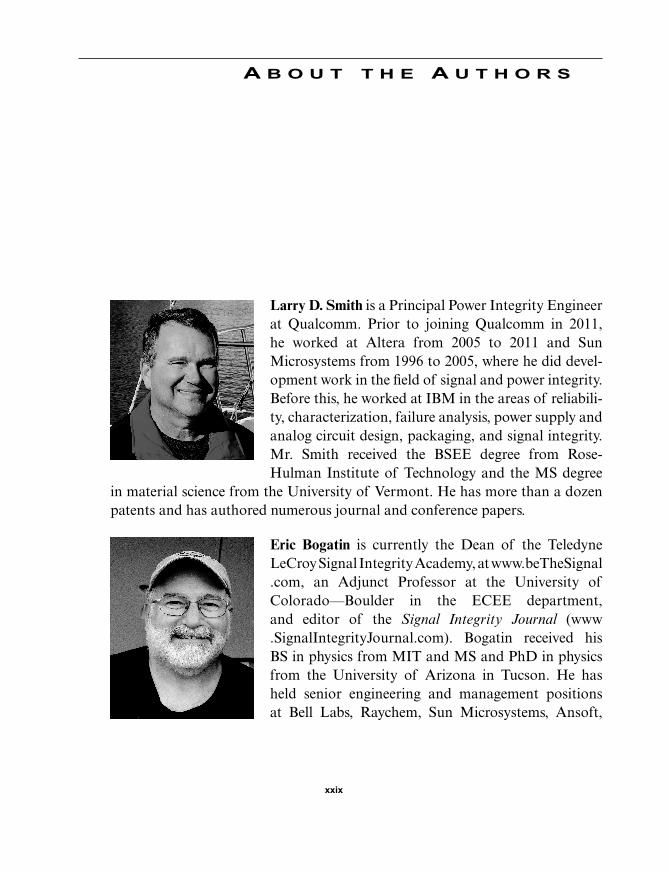
Larry D. Smith is a Principal Power Integrity Engineer at Qualcomm. Prior to joining Qualcomm in 2011, he worked at Altera from 2005 to 2011 and Sun Microsystems from 1996 to 2005, where he did devel-opment work in the fi eld of signal and power integrity. Before this, he worked at IBM in the areas of reliabili-ty, characterization, failure analysis, power supply and analog circuit design, packaging, and signal integrity. Mr. Smith received the BSEE degree from Rose- Hulman Institute of Technology and the MS degree
in material science from the University of Vermont. He has more than a dozen patents and has authored numerous journal and conference papers.
Eric Bogatin is currently the Dean of the Teledyne LeCroy Signal Integrity Academy, at www.beTheSignal.com, an Adjunct Professor at the University of Colorado—Boulder in the ECEE department, and editor of the Signal Integrity Journal (www.SignalIntegrityJournal.com). Bogatin received his BS in physics from MIT and MS and PhD in physics from the University of Arizona in Tucson. He has held senior engineering and management positions at Bell Labs, Raychem, Sun Microsystems, Ansoft,
9780132735551_print.indb xxix9780132735551_print.indb xxix 23/02/17 9:07 PM23/02/17 9:07 PM

and Interconnect Devices. He has written six technical books in the fi eld and presented classes and lectures on signal integrity worldwide. In 2011, his company Bogatin Enterprises, which he founded with his wife Susan in 1990, was acquired by Teledyne LeCroy. After concluding his live public classes in 2013, he devoted his efforts into creating the Signal Integrity Academy, a web portal to provide all of his classes and training content online for individuals and for companies. In addition to lecturing and writing on signal and power integrity topics, Bogatin also writes science fi ction novels. The fi rst in a series, Shadow Engineer, was published in 2016.
xxx About the Authors
9780132735551_print.indb xxx9780132735551_print.indb xxx 23/02/17 9:07 PM23/02/17 9:07 PM

1
C H A P T E R 1
Engineering the Power Delivery Network
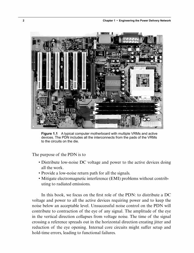
1.1 What Is the Power Delivery Network (PDN) and Why Should I Care?The power delivery network consists of all the interconnects in the power supply path from the voltage regulator modules (VRMs) to the circuits on the die. Generally, these include the power and ground planes in the boards, cables, connectors, and all the capacitors associated with the power supply. Figure 1.1 is an example of a typical computer board with multiple VRMs and paths delivering the power and ground to the pads of all the active devices.
9780132735551_print.indb 19780132735551_print.indb 1 23/02/17 9:07 PM23/02/17 9:07 PM
2 Chapter 1 • Engineering the Power Delivery Network
Figure 1.1 A typical computer motherboard with multiple VRMs and active devices. The PDN includes all the interconnects from the pads of the VRMs to the circuits on the die.
The purpose of the PDN is to
• Distribute low-noise DC voltage and power to the active devices doing all the work.
• Provide a low-noise return path for all the signals.• Mitigate electromagnetic interference (EMI) problems without contrib-
uting to radiated emissions.
In this book, we focus on the fi rst role of the PDN: to distribute a DC voltage and power to all the active devices requiring power and to keep the noise below an acceptable level. Unsuccessful noise control on the PDN will contribute to contraction of the eye of any signal. The amplitude of the eye in the vertical direction collapses from voltage noise. The time of the signal crossing a reference spreads out in the horizontal direction creating jitter and reduction of the eye opening. Internal core circuits might suffer setup and hold-time errors, leading to functional failures.
9780132735551_print.indb 29780132735551_print.indb 2 23/02/17 9:07 PM23/02/17 9:07 PM
What Is the Power Delivery Network (PDN) and Why Should I Care? 3
T I P The consequence of not correctly designing the PDN is increased bit error ratios from enhanced vertical noise and jitter on both I/O circuits and internal-to-the-chip circuits. Excessive horizontal noise in core circuits might lead to setup and hold-time violations.
Depending on the circuit of the switching gates, the PDN noise will add to the signal coming from the transmitter (TX). This can also appear as noise on the voltage reference at the receiver (RX). In both cases, the PDN noise will reduce the noise margin available from other sources.
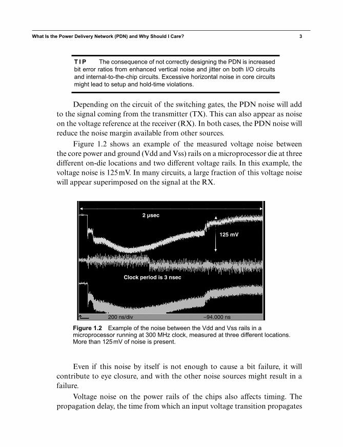
Figure 1.2 shows an example of the measured voltage noise between the core power and ground (Vdd and Vss) rails on a microprocessor die at three different on-die locations and two different voltage rails. In this example, the voltage noise is 125 mV. In many circuits, a large fraction of this voltage noise will appear superimposed on the signal at the RX.
2 µsec
Clock period is 3 nsec
200 ns/div –94.000 ns
125 mV
Figure 1.2 Example of the noise between the Vdd and Vss rails in a microprocessor running at 300 MHz clock, measured at three different locations. More than 125 mV of noise is present.
Even if this noise by itself is not enough to cause a bit failure, it will contribute to eye closure, and with the other noise sources might result in a failure.
Voltage noise on the power rails of the chips also affects timing. The propagation delay, the time from which an input voltage transition propagates
9780132735551_print.indb 39780132735551_print.indb 3 23/02/17 9:07 PM23/02/17 9:07 PM
4 Chapter 1 • Engineering the Power Delivery Network
through the sequence of gates contributing to an output voltage transition, depends on the instantaneous voltage level between the In CMOS technology, the higher the drain-to-source voltage, the larger the electric fi elds in the chan-nels and the shorter the propagation delay. Likewise, the lower the Vdd to Vss voltage, the longer the propagation delay.
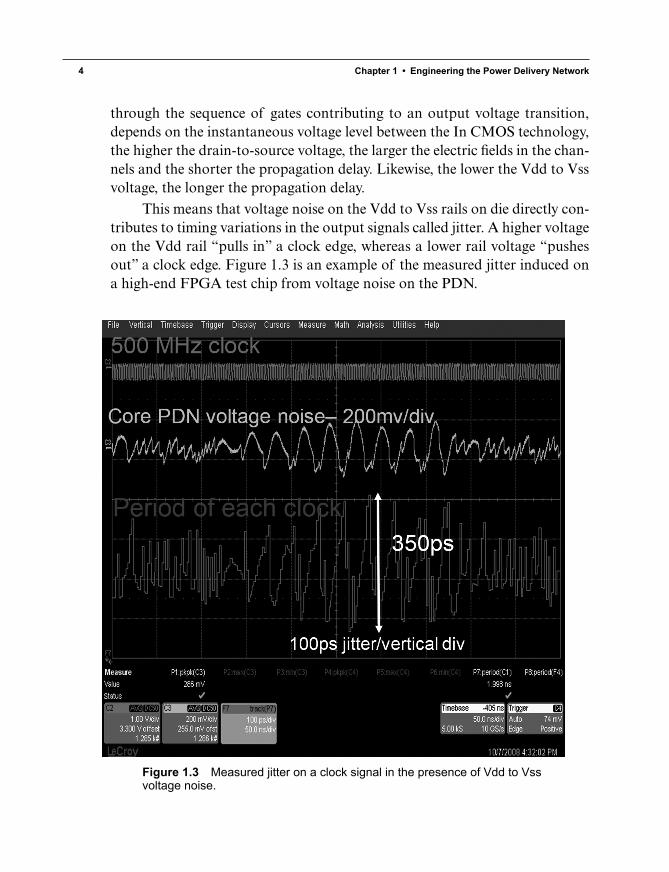
This means that voltage noise on the Vdd to Vss rails on die directly con-tributes to timing variations in the output signals called jitter. A higher voltage on the Vdd rail “pulls in” a clock edge, whereas a lower rail voltage “pushes out” a clock edge. Figure 1.3 is an example of the measured jitter induced on a high-end FPGA test chip from voltage noise on the PDN.
Figure 1.3 Measured jitter on a clock signal in the presence of Vdd to Vss voltage noise.
M01_Bogatin_Ch01_p001-016.indd 4M01_Bogatin_Ch01_p001-016.indd 4 23/02/17 9:14 PM23/02/17 9:14 PM
Engineering the PDN 5
In this example, a clock distribution net shares the Vdd rail with a number of other gates. These gates were switching with a pseudo-random bit sequence (PRBS), drawing large currents from the PDN and generating large transient voltage noise. This voltage noise, as applied to the clock distribution network gates, caused timing variations in the clock signal. The period jitter measure-ment, the period of time from one clock edge to the next clock edge, appears as the period of each clock. This measurement demonstrates the direct correla-tion between the voltage noise on the die and the jitter on the clock.
In this example, the sensitivity of the jitter from PDN noise is about 1 ps of jitter per mV of voltage noise. A 100 mV peak-to-peak PDN noise would contribute to 100 ps peak-to-peak jitter. In a 2 GHz clocked system, the period is only 500 psec. The jitter from the PDN noise alone would consume the entire timing budget.
T I P In this example, the jitter sensitivity to PDN noise is about 1 ps/mV. This is a rough estimate of the sensitivity to expect in many devices.
1.2 Engineering the PDNTo meet both voltage noise and the timing budgets, the voltage noise on the PDN must be kept below some specifi ed value. Depending on the system details, this voltage noise limit is roughly about ±5% of the supply voltage. In typical CMOS-based digital systems with single-ended signals, the total noise margin for the receiver is about 15% of the signal swing. Unless there is a com-pelling reason not to do so, we usually partition this budget equally between the three dominate sources of noise: refl ection noise, crosstalk, and PDN noise. This is the origin of the typical specifi cation being 5% PDN noise allowed.
In some applications, such as analog-to-digital converters (ADCs) or phase locked loops (PLLs), performance is very sensitive to voltage noise and the PDN noise must be kept below 1%. The voltage noise must be kept below the limits from DC all the way up to the bandwidth of the signals, which might be as high as 5 GHz to 10 GHz.
As with all signal integrity problems, the fi rst step in eliminating them is to identify the root cause. At low frequency, the voltage noise across the PDN is usually due to the voltage noise from the VRM and so the fi rst step in PDN design is selecting a VRM with low enough voltage noise under a suitable load current.
9780132735551_print.indb 59780132735551_print.indb 5 23/02/17 9:07 PM23/02/17 9:07 PM

6 Chapter 1 • Engineering the Power Delivery Network
However, even with the world’s most stable VRM, voltage noise still exists on the pads of the die. This arises from the voltage drop across the impedance of the entire PDN from transient power currents through the gates on the die. Between the pads of the VRM and the pads on the die are all the interconnects associated with the PDN. We refer to this entire network as the PDN ecology.
T I P The PDN ecology is the entire series of interconnects from the pads on the die to the pads of the VRM. These all interact to create the impedance profi le applied to the die and infl uence PDN noise.
As applied to the pads of the die, these interconnects contribute to an impedance profi le. Figure 1.4 shows a typical example.
1
1E1
1E–1
1E–2
1E–3
Impe
danc
e, Ω
1E3 1E4 1E5 1E6 1E7 1E8 1E9
Frequency, Hz
Figure 1.4 Example of an impedance profi le of the entire PDN ecology, as applied to the pads of the die.
Any transient currents through this impedance profi le generates voltage noise on the pads of the chip, independent of the VRM stability.
For example, Figure 1.5 shows the transient current spectrum drawn by the core power rail for a device when executing a specifi c microcode. Super-imposed on the current spectrum is the impedance profi le through which this current fl ows. The combination of the current amplitude and impedance at each frequency generates a voltage noise spectrum. This noise spectrum, when viewed in the time domain, results in a transient voltage noise.
9780132735551_print.indb 69780132735551_print.indb 6 23/02/17 9:07 PM23/02/17 9:07 PM

Engineering the PDN 7
1.3
1.2
1.1
1.0
0.9
0.8
0.7
0.0 0.2 0.4 0.6 0.8 1.0
Volt
age
on
ch
ip1.3
1.2
1.1
1.0
0.9
0.8
0.7
Volt
age
on
ch
ip
Time, µsec0.0 0.2 0.4 0.6 0.8 1.0
Time, µsec
“Working” “Failed!”
1
1E1
1E–1
1E–2
1E–3
1
1E1
1E–1
1E–2
1E–31E2 1E3 1E4 1E5 1E6 1E7 1E8 1E9
Frequency, Hz1E2 1E3 1E4 1E5 1E6 1E7 1E8 1E9
Frequency, Hz
Cur
rent
, im
peda
nce
Cur
rent
, im
peda
nce
Figure 1.5 Left Side: PDN impedance profi le and transient current spectrum result in acceptable voltage noise. Right Side: Slight change in current spectrum gives unacceptable voltage noise.
The left side of Figure 1.5 shows the transient current spectrum, PDN impedance profi le, and resulting voltage noise on the power rail. This com-bination of current spectral peaks and impedance peaks results in acceptable noise. On the right is the same impedance profi le, but with slightly different microcode algorithm driving the same gates at a slightly different frequency. A current spectral peak ended up overlapping a larger impedance peak and generating a rail voltage noise above the acceptable limit.
The actual voltage noise generated by the transient current through the impedance profi le depends on the overlap of the current frequency components and the peaks in the impedance profi le. If the voltage noise is below a specifi ed level, PDN induced errors will not occur. If the microcode changes resulting current amplitude peaks and frequency component changes, their overlap with impedance peaks might create more voltage noise and product failure.
T I P The noise on the PDN depends as much on the impedance profi le applied to the die as the spectrum of the transient current through the die. Microcode details and gate utilization have a strong impact on the PDN noise generated.
9780132735551_print.indb 79780132735551_print.indb 7 23/02/17 9:07 PM23/02/17 9:07 PM

8 Chapter 1 • Engineering the Power Delivery Network
1.3 “Working” or “Robust” PDN DesignThe variability in performance due to the specifi c microcode driving the switching of on-die gates makes testing a product for adequate PDN design diffi cult. A product might work just fi ne at boot up, or when running a specifi c software test suite if the combination of current spectral peaks and impedance peaks results in less than the specifi ed transient noise. The product design may “pass” this test and be stamped as “working.”
However, if another software suite were to run that drives more gates and causes them to switch at a different dominant loop frequency, which coincidently overlaps a peak in the PDN impedance profi le, larger instanta-neous voltage drops might result and the same product could fail.
Although having the product boot up, run a test suite and apparently work is encouraging, it does not guarantee “robust” operation. Products often “work” in evaluation but have fi eld failures when driven by a broad range of customer software.
A robust PDN design means that any software code may run and gener-ate the maximum transient current at any arbitrary frequency with any time domain signature. The resulting worst-case voltage generated by this current through the impedance profi le is always less than an amount that would cause a failure.
The combination of the worst-case transient current and the voltage noise specifi cation work together to set a limit for the maximum allowable PDN impedance such that the voltage noise will never exceed the specifi cation.
This maximum allowable PDN impedance with guaranteed performance is referred to as the target impedance in PDN design, and we derive it with [1]
ZV
Itargetnoise
max transient
= Δ−
(1.1)
where
Ztarget = the maximum allowable PDN impedance at any frequency
∆Vnoise = the maximum specifi ed voltage rail noise to meet performance requirements
Imax-transient = the worst-case transient current under any possible operation
9780132735551_print.indb 89780132735551_print.indb 8 23/02/17 9:07 PM23/02/17 9:07 PM
“Working” or “Robust” PDN Design 9
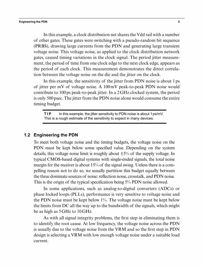
For example, if the noise spec is set as ±50 mV and the worst-case tran-sient current is 1 A, the target impedance is
ZV
I0.05V
1A50 mtarget
noise
max transient
= Δ = = Ω−
(1.2)
If either ∆Vnoise or Imax-transient is a function of frequency, then Ztarget is a function of frequency.
In principle, the combination of the entire spectral distribution of cur-rents and the entire impedance profi le is what creates the worst-case peak voltage noise. Unfortunately, this can only be determined with a transient sim-ulation including the details of the transient current waveform and the imped-ance profi le of the entire PDN. In practice, the target impedance is a useful approximation as a fi gure of merit to help focus the design of the PDN on a good starting place.
T I P The target impedance is a useful fi gure of merit for the PDN. It is a good approximation of a design goal for a robust PDN design. The fi nal evaluation of robust PDN design would come from a transient simulation of the entire PDN and the transient current waveforms.
A fully robust PDN is defi ned by this target impedance. If the impedance of the entire PDN ecology, as applied to the pads of the die, is below the tar-get impedance at all frequencies, the maximum worst-case rail collapse noise generated by the transient current fl owing through the PDN impedance will not exceed the noise spec except in a very rare rogue wave situation. Figure 1.6 shows an example of the impedance profi le below the target impedance of 50 mΩ at all frequencies and an example of the resulting rail voltage noise with a high current load.
T I P The target impedance is the most important metric when evaluating PDN performance. The farther the PDN impedance is above the target impedance, the greater the risk of a failure.
9780132735551_print.indb 99780132735551_print.indb 9 23/02/17 9:07 PM23/02/17 9:07 PM

10 Chapter 1 • Engineering the Power Delivery Network
Target impedance
PDN impedance profile
Power rail voltage
Transient chip current
Vol
tage
Frequency, Hz
Impe
danc
e, Ω
1E2 1E3 1E4 1E5 1E6 1E7 1E8 1E9 1E10
1E–3
1E–2
1E–1
1E1
1
1.2
1.0
0.8
0.6
0.4
0.2
0.0
–0.2
0 20 40 60 80 100Time, nsec
Figure 1.6 Top: The impedance profi le of the PDN ecology engineered to be below the target impedance from DC up to a very high bandwidth. Bottom: The resulting Vdd rail noise under large transient current load showing the noise is always below the 5% spec limit. The square wave trace is the transient current as driven by a clock. It is plotted on a relative scale.
In practice, the maximum, worst-case transient current through the die will not be fl at at all frequencies. The maximum current amplitude generally drops off at the high-frequency end, related to how quickly the maximum number of switching gates can be turned on. The precise details depend on the chip architecture, the number of bits in the pipeline, and the nature of the microcode. The effective rise time could be from the rise time of the clock edge to 100 clock cycles.
For example, if the clock frequency is 2 GHz, with a 0.5 ns clock period, and the maximum number of switching gates requires 20 cycles to build up, the shortest rise time for the turn on of the worst-case transient current would be 0.5 ns × 20 cycles = 10 ns. The amplitude of the maximum transient current frequency components will begin to roll off above about 0.35/10 ns = 35 MHz.
9780132735551_print.indb 109780132735551_print.indb 10 23/02/17 9:07 PM23/02/17 9:07 PM

“Working” or “Robust” PDN Design 11
Above 35 MHz, the worst-case transient current spectrum would drop off at −20 dB/decade and the resulting target impedance would increase with fre-quency. The target impedance, in this example, assuming a 50 mV rail voltage noise spec and worst-case current amplitude of 1 A, is shown in Figure 1.7.
Frequency, Hz
Targ
et im
ped
ance
, Ω
1.E+04 1.E+05 1.E+06 1.E+07 1.E+08 1.E+09 1.E+10
100
10
1
0.1
0.01
Figure 1.7 Target impedance when the transient current turns on in 20 clock cycles to a maximum of 1 A.
The consequence of this behavior is that the target impedance spec is relaxed at higher frequency. Estimating where this knee frequency begins is often diffi cult unless we know the details of the transient current and worst-case microcode.
This analysis points out that, in practice, accurately calculating the tran-sient currents and the precise requirements for the target impedance of the PDN is extremely diffi cult. One must always apply engineering judgment in translat-ing the information available into the requirements for a cost-effective design.
The process to engineer the PDN is to
• Establish a best guess for the target impedance based on what is known about the functioning and applications of the chips.
• Make engineering decisions to try to meet this impedance profi le where possible.
• Balance the trade-offs between the cost of implementing the PDN impedance compared to the target impedance, and the risk of a fi eld failure.
9780132735551_print.indb 119780132735551_print.indb 11 23/02/17 9:07 PM23/02/17 9:07 PM
12 Chapter 1 • Engineering the Power Delivery Network
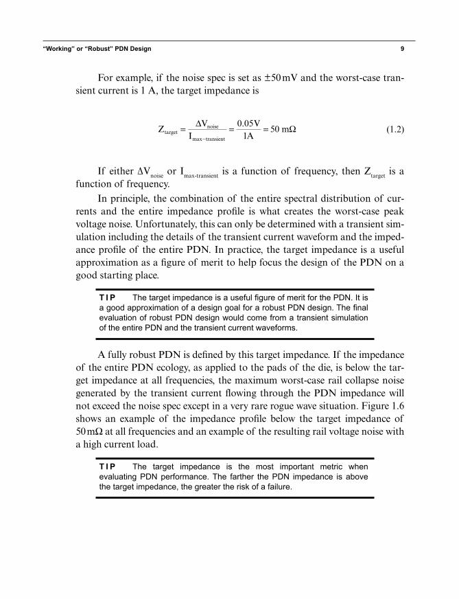
A rough measure of the risk of a failure of circuits to run at rated per-formance is the ratio of the actual PDN impedance to the target impedance, termed the PDN ratio:
=PDN ratioActual PDN Impedance
Target Impedance (1.3)
A ratio of less than 1 indicates low risk of a PDN-related failure. As this ratio increases, the risk increases as well. From practical experience, a ratio of 2 might still offer an acceptable risk, but a ratio of 10 will almost surely result in unacceptable risk. Even though many microcodes run at rated performance, some are likely to stimulate the PDN resonance and generate product stability issues.
Generally, achieving a lower impedance PDN, and consequently a lower risk ratio, costs more either due to more components required, tighter assembly design rules impacting yield, more layers in the board or package, increased area for die capacitance, or the use of more expensive materials. The balance between cost and risk is often a question of how much risk you are comfortable with. By paying more for added design margin, you can always “buy insurance” and reduce the risk. This is the fundamental trade-off in PDN design.
T I P An important metric of risk in PDN design is the PDN ratio, which is the ratio of the peak impedance to the target impedance. A PDN ratio of 2 or lower is a low risk whereas a PDN ratio of 10 or more is a high risk.
In consumer applications, often strongly cost driven, engineering for a higher risk ratio with a lower cost design might be a better balance. However, in avionic systems, for example, paying extra for a risk ratio less than 1 might be the cost-effective solution. Different applications have a different balance between cost and risk ratio.
1.4 Sculpting the PDN Impedance Profi leThe goal in PDN design is to engineer an acceptable impedance profi le from DC to the highest frequency component of any power rail currents. All the elements of the PDN should be engineered together to sculpt the
9780132735551_print.indb 129780132735551_print.indb 12 23/02/17 9:07 PM23/02/17 9:07 PM
Sculpting the PDN Impedance Profi le 13
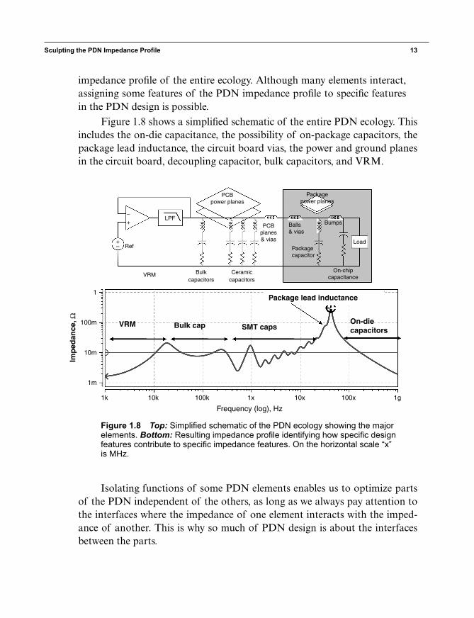
impedance profi le of the entire ecology. Although many elements interact, assigning some features of the PDN impedance profi le to specifi c features in the PDN design is possible.
Figure 1.8 shows a simplifi ed schematic of the entire PDN ecology. This includes the on-die capacitance, the possibility of on-package capacitors, the package lead inductance, the circuit board vias, the power and ground planes in the circuit board, decoupling capacitor, bulk capacitors, and VRM.
Ref
LPFBalls& vias
Bulk cap SMT capsOn-diecapacitors
VRM
Imp
edan
ce, Ω
Package lead inductance
On-chipcapacitance
Packagecapacitor
Bumps
Load
Packagepower planes
PCBplanes& vias
PCBpower planes
VRM Ceramiccapacitors
Bulkcapacitors
100m
1
10m
1m
Frequency (log), Hz
1k 10k 100k 1x 10x 100x 1g
+–
+–
Figure 1.8 Top: Simplifi ed schematic of the PDN ecology showing the major elements. Bottom: Resulting impedance profi le identifying how specifi c design features contribute to specifi c impedance features. On the horizontal scale “x” is MHz.
Isolating functions of some PDN elements enables us to optimize parts of the PDN independent of the others, as long as we always pay attention to the interfaces where the impedance of one element interacts with the imped-ance of another. This is why so much of PDN design is about the interfaces between the parts.
9780132735551_print.indb 139780132735551_print.indb 13 23/02/17 9:07 PM23/02/17 9:07 PM

14 Chapter 1 • Engineering the Power Delivery Network
In the journey ahead, we explore each of these elements that make up the PDN and how they interact to result in a robust and cost-effective PDN design. Ultimately, the power integrity engineer is responsible for fi nding an acceptable balance between cost, risk, performance, and schedule. The more we know about the details of the specifi c PDN elements, the more quickly we can reach an acceptable solution.
1.5 The Bottom Line 1. The PDN consists of all the interconnects from the pads on the die to
the VRM and all of the components in between. 2. The purpose of the PDN is to provide a clean, low-noise voltage and
ground supply to the devices and a low impedance return path for signals, and to mitigate EMC problems.
3. The typical noise spec on the PDN of 5% tolerance is based on an allocation of 1/3 the noise budget to each of the main sources of noise: refl ection noise, cross talk, and PDN.
4. Voltage noise on the PDN is a result of transient power currents pass-ing through the impedance of the PDN. The amount of noise is due to the combination of the impedance profi le and the transient current spectrum.
5. Noise on the PDN can contribute to jitter. A typical value of the sensitivity is 1 psec/mV of noise. This number varies depending on the chip design and device technology node.
6. The impedance profi le, as applied to the chip pads, is the most important metric for the quality and performance of the PDN. This is from DC to the highest frequency components of the switching signals.
7. The target impedance is a measure of the maximum impedance, which will keep the worst-case voltage noise below the acceptable spec.
8. The PDN ratio is the ratio of the actual PDN peak impedance to the target impedance. It is a good metric of risk. A PDN ratio greater than 10 is a high-risk design.
9. Sculpting the impedance profi le requires optimizing both the individual elements of the PDN and their interactions. The entire PDN ecology must be optimized to reduce the peak values.
10. If you care about PDN design, this book is for you.
9780132735551_print.indb 149780132735551_print.indb 14 23/02/17 9:07 PM23/02/17 9:07 PM

15
R E F E R E N C E
[1] L. D. Smith, R. E. Anderson, D. W. Forehand, T. J. Pelc, and T. Roy, “Power distribution system design methodology and capacitor selection for modern CMOS technology,” IEEE Trans. Adv. Packag., vol. 22, no. 3, pp. 284–291, 1999.
9780132735551_print.indb 159780132735551_print.indb 15 23/02/17 9:07 PM23/02/17 9:07 PM

9780132735551_print.indb 169780132735551_print.indb 16 23/02/17 9:07 PM23/02/17 9:07 PM
761
I N D E X
Numbers0th droop. See clock edge current1-inch diameter copper loop, measuring
impedance of, 102–1051st droop, 6612nd droop, 6613D fi eld solver
0th droop, 195–202extracting spreading inductance from,
304–3064-point Kelvin resistance measurement
technique, 93–95182 nF ideal capacitor, 27–290603 multilayer ceramic chip (MLCC)
capacitor, 27
AAconductor, 343, 370Adielectric, 344, 370abAmps, 146abHenrys, 146AC steady state responses, 589–595AC tolerance, 660ADCs (analog-to-digital converters), 5ADS (Advanced Design System), 22, 84–85
Agilent Technologies, 22Ampere’s Law, 168analog-to-digital converters (ADCs), 5approximations, inductance
parallel plate approximation for loop inductance, 183
round loop inductance, 179–182uniform transmission line inductance,
188–193artifacts in impedance measurements,
105–109measured inductance of a via, 109–114small MLCC capacitor on board,
114–119Atotal, 343attenuation, modal resonance and, 343–347
BB (magnetic fi eld density), 155–159back emf (electromotive force), 149ball grid array (BGA), 240Bandini Fertilizer Company, 448Bandini Mountain
characteristic impedance, 456–457frequency, 452–456
9780132735551_print.indb 7619780132735551_print.indb 761 23/02/17 9:13 PM23/02/17 9:13 PM
762 Index
intrinsic damping, 456–460overview of, 447–452peak impedance, 451–452, 494reduced loop inductance, 718–722
BGA (ball grid array), 240boundary conditions, 337–338building PDN (power delivery network)
ecology, 488–492bulk capacitance, 225–229
minimum amount of capacitance required, 478–483
optimizing, 483–487
Ccapacitance. See also capacitors
bulk capacitance, 225–229minimum amount of capacitance
required, 476–478optimizing, 483–487
capacitance referenced to both Vss and Vdd rails, 558–562
defi nition of, 138density, 435fringe fi eld capacitance
overview of, 279–285in power puddles, 285–289
gate, 430MLCC (multilayer ceramic chip)
capacitors, 220–222ODC (on-die decoupling capacitance)
clock edge noise, 431ESR (equivalent series resistance),
436–439estimating, 431–435historic trends in, 435–436measuring, 434–435relaxation time, 438sources of, 430
on-die capacitancelarge on-die capacitance with small
package lead inductance, 521–527
measuring impedance of, 120–134overview of, 138–140parallel plate capacitance, 278–279
capacitor mounting inductance, 401–403capacitors. See also capacitance; impedance;
MLCC (multilayer ceramic chip) capacitors
bulk capacitorsminimum amount of capacitance
required, 476–478optimizing, 483–487
capacitor mounting inductance, 401–403
capacitor/cavity interaction, 325–327classes of, 222controlled ESR capacitors, 527–532damping to suppress parallel resonant
peaks, 403–408DC blocking capacitors
number required to suppress cavity resonance, 387–393
number to carry return current, 393–401
overview of, 383–386ESL (equivalent series inductance), 207ESR (equivalent series resistance), 207,
229–234FDTIM (Frequency Domain Target
Impedance Method)selecting capacitor values with,
516–521selecting number of capacitors with,
514–516location, spreading inductance and,
327–332lossy transmission line models,
260, 269–272OPD (on-package decoupling
capacitors), 532–539, 724–731real versus ideal, 26–30, 206reverse aspect ratio capacitors, 246
9780132735551_print.indb 7629780132735551_print.indb 762 23/02/17 9:13 PM23/02/17 9:13 PM
Index 763
SCL (Switched Capacitor Load)impulses from, 613–622
PRC (PDN Resonance Calculator) spreadsheet, 694–696
X2Y capacitors, 248–250cavity
capacitor/cavity interaction, 325–327cavity modes in two dimensions, 347–353defi nition of, 275fringe fi eld capacitance
overview of, 279–285in power puddles, 285–289
impedance profi les, 276–277long, narrow cavities, loop inductance in,
290–292modal resonances, 334–340parallel plate capacitance, 278–279parameters, 370PCB cavity
impedance as seen by die pads, 465–469role of, 469–476S-parameters, 461–462VRM (voltage regulator module),
460–465peak impedance, 364–367series LC resonance, 312–314signal integrity design
capacitor mounting inductance, 401–403
cavity losses and impedance peak reduction, 408–411
damping to suppress parallel resonant peaks, 403–408
DC blocking capacitors to carry return current, 393–397
DC blocking capacitors to suppress cavity resonance, 383–393
lower impedance and higher damping, 367–371
multiple capacitor values, 411–414shorting vias, 372–383
suboptimal numbers of DC capacitors, 397–401
summary of, 418–419thin dielectric, 367–371transmission line circuit models,
419–423uncontrolled ESR capacitors, 414–417
spreading inductancecapacitor location and, 327–332between contact points, 317–324extracting from 3D fi eld solver,
304–306probing with transfer impedance,
353–360role of, 327–332saturating, 332–334source contact location, 315–317in wide cavities, 292–304
transmission line properties, 334–340Cbulk, 226, 480Ccap, 262Ccavity, 375, 402, 422Cdie, 50Cdown, 634cgs units, 146characteristic impedance, 33, 335
Bandini Mountain, 456–457calculating, 574, 647
charge, 139. See also capacitancecheckerboard reduction factor, 669–671circuits. See also impedance
circuit topology, identifying, 46–52lumped circuit
PRF (parallel resonant frequency), 307–312
SRF (series resonance frequency), 307–312
models for real capacitors, 206–209parallel RLC circuits
ESR (equivalent series resistance), 229–237
9780132735551_print.indb 7639780132735551_print.indb 763 23/02/17 9:13 PM23/02/17 9:13 PM
764 Index
examples of, 42–46impedance of, 34–35impedance profi les, 209resonant properties of, 36–42
series RLC circuitsexamples of, 42–46impedance of, 30–33resonant properties of, 36–42
Class 1 capacitors, 222Class 2 capacitors, 222–223Class 3 capacitors, 222–223CLen, 298CLen-fringe, 286CLen-fringe-image, 280CLen-image, 280CLen-pp, 286CLen-pp-image, 280, 281CLen-total, 286Cload, 432clock edge current
capacitance referenced to both Vss and Vdd rails, 558–562
as cause of PDN noise, 565–572clock edge droop, 579, 683–684clock edge noise, 431, 557–558, 661–664example of, 557–558impulses from SCL (Switched Capacitor
Load), 613–622measurement example: embedded
controller processor, 562–565waveforms composed of series of clock
impulses, 622–629clock edge droop, 579, 683–684clock gating, 629–633clock swallowing, 629–633CMEs (coronal mass ejections), 156–157cobalt, 147, 168CODC, 432, 453combining capacitors in parallel, 209–211constant current amplitude, 22–23constricting resistance, 93
contact points, spreading inductance between, 317–324
contact resistanceconstricting, 93ESR (equivalent series resistance), 118four-point Kelvin resistance measurement
technique, 93–95traditional two-wire resistance
measurements, 94controlled ESR capacitors, 238–240,
527–532copper loop, measuring impedance of,
102–105core power rails. See Vdd railscoronal mass ejections (CMEs), 156–157Coulombs, 143Cpp, 284, 286Cpp-image, 281Csect, 262Ctotal, 284Cup, 634current
clock edge currentcapacitance referenced to both Vss
and Vdd rails, 558–562as cause of PDN noise, 565–572clock edge droop, 579, 683–684clock edge noise, 431, 557–558,
661–664example of, 557–558impulses from SCL (Switched
Capacitor Load), 613–622measurement example: embedded
controller processor, 562–565waveforms composed of series of
clock impulses, 622–629current waveforms, 577–579
impulse current waveform, 577, 579–581, 613–629, 696–702
resonance current waveform, 577, 585–589
9780132735551_print.indb 7649780132735551_print.indb 764 23/02/17 9:13 PM23/02/17 9:13 PM
Index 765
rogue wave effect, 602–613step current waveform, 577, 582–584
inrush current, 633–634leakage current, 659max current consumed, 659maximum dynamic current, 659minimum current consumed, 659minimum dynamic current, 659PRC (PDN Resonance Calculator)
spreadsheet, 658–661ratio of voltage to. See impedancethrough ideal capacitor, 19transient currents
calculating target impedance with, 550–553
clock gating, 629–633clock swallowing, 629–633estimating, 646importance of, 547–549impulse current waveform, 579–581on-die PDN current draw, 553–558peak impedance, 595–602power gating, 633–638PRC (PDN Resonance Calculator)
spreadsheet, 731–738q-factor, 595–602reactive elements, 595–602resonance current waveform, 585–589rogue wave effect, 602–613step current waveform, 582–584target impedance, 589–595
current waveforms, 577–579impulse current waveform
defi nition of, 577impulses from SCL (Switched
Capacitor Load), 613–622PDN response to, 579–581PRC (PDN Resonance Calculator)
spreadsheet, 696–702waveforms composed of series of
clock impulses, 622–629
resonance current waveformdefi nition of, 577PDN response to, 585–589
rogue wave effect, 602–613step current waveform
defi nition of, 577PDN response to, 582–584
Ddamping
Bandini Mountain, 456–460lower impedance and, 367–371PRC (PDN Resonance Calculator)
spreadsheet, 685–693suppressing parallel resonant peaks
with, 403–408dB, 166DC blocking capacitors
number to carry return current, 393–397number to suppress cavity resonances,
387–393overview of, 383–386suboptimal numbers of DC capacitors,
397–401Dcavity, 305, 310decoupling
controlled ESR capacitors, 527–532OPD (on-package decoupling
capacitors), 532–539density
capacitance density, 435energy density in magnetic fi eld, 159–162inductance density, 162magnetic fi eld density (B), 155–159power density, 435
densitycaps, 395densitysig, 395design (PDN)
goals of, 643–645power integrity principles, summary of,
645–653
9780132735551_print.indb 7659780132735551_print.indb 765 23/02/17 9:13 PM23/02/17 9:13 PM
766 Index
PRC (PDN Resonance Calculator) spreadsheet
clock edge noise and on-die parameters, 661–664
goal of, 658impulse, step, and resonance response,
696–702inductance, analyzing board and
package geometries for, 674–677input voltage, current, and target
impedance parameters, 658–661mounting inductance and resistance,
665–673OPD (on-package decoupling
capacitors), 724–731overview of, 654–658performance fi gures of merit,
682–685q-factors in frequency and time
domains, 703–710reduced loop inductance, 718–722reverse-engineering of PDN from
measurements, 740–747rise time and stimulation of
impedance peak, 710–717risk, performance, and cost
tradeoffs, 739SCL (Switched Capacitor Load)
model, 694–696signifi cance of damping and q-factors,
685–693simulated and measured PDN
impedance and voltage features, 754–757
simulation-to-measurement correlation, 747–754
SMPS (switch mode power supply) model, 722–724
three loops of, 677–682
transient current assumptions, 736–738
transient response of PDN, 731–735robust design, 8–12rogue waves and, 610–613working design, 8–12
device under test (DUT), 70Df, 229diamagnetic properties, 146–147die pads, impedance and, 465–469dielectric
impact on magnetic fi eld lines, 146–147thickness of, 367–371
dielectric constant (Dk), 180, 370–371, 376, 422
diffusion junctions, 430DIP (dual in-line package), two leads in,
81–85dispersion (material), 288Dk (dielectric constant), 180, 370–371,
376, 422Dkeff, 189dl, 166dL/dv, 161dLLoop, 301domains
frequency domain, 428–430FDTIM (Frequency Domain Target
Impedance Method), 514–521impedance in, 18–21PRC (PDN Resonance Calculator)
spreadsheet, 703–710time domain
current through ideal capacitor, 19impedance in, 19PRC (PDN Resonance Calculator)
spreadsheet, 703–710driving a resonance, 337DUT (device under test), 70
9780132735551_print.indb 7669780132735551_print.indb 766 23/02/17 9:13 PM23/02/17 9:13 PM

Index 767
Dvia, 305, 310dynamic current
impulse current waveformdefi nition of, 577PDN response to, 579–581
resonance current waveformdefi nition of, 577PDN response to, 585–589
rogue wave effect, 602–613step current waveform
defi nition of, 577PDN response to, 582–584, 585–589
Ee (energy density in magnetic fi eld),
159–162ecology (PDN). See PDN (power delivery
network) ecologyeffective dielectric constant, 189EIA (Electronics Industries Alliance), 223electromagnetic compatibility (EMC), 364ElectroMagnetic Units (EMU), 146Electronics Industries Alliance (EIA), 223embedded controller processor, measuring
clock edge currents in, 562–565EMC (electromagnetic compatibility), 364EMU (ElectroMagnetic Units), 146energy density in magnetic fi eld, 159–162equivalent circuit models for real capacitors,
206–209equivalent series inductance (ESL), 118, 207equivalent series resistance. See ESR
(equivalent series resistance)ESL (equivalent series inductance),
118, 207, 516ESR (equivalent series resistance), 118, 207
calculating, 681controlled ESR capacitors, 238–240,
527–532
effective ESR, 403–408estimating from spec sheets, 234–237fi rst and second order models, 229–234ODC (on-die decoupling capacitance),
436–439package PDN (power delivery network),
446estimating
ESR (equivalent series resistance), 234–237ODC (on-die decoupling capacitance),
431–435transient currents, 646
external inductance, 167–172
FFclock, 453–454FDTIM (Frequency Domain Target
Impedance Method)selecting capacitor values with, 516–521selecting number of capacitors with,
514–516ferrite materials, 147ferromagnetic materials, 147, 168fi eld lines, fl ux of, 144–147fi elds, magnetic
energy density in, 159–162fringe fi eld capacitance
overview of, 279–285in power puddles, 285–289
inductanceinductor impedance, 147–150in long, narrow cavities, 290–292magnetic fi eld density (B), 155–159principles of, 141–147quasi-static approximation, 150–155spreading inductance in wide cavities,
292–304mutual fi eld lines, 173self-fi eld lines, 173
9780132735551_print.indb 7679780132735551_print.indb 767 23/02/17 9:13 PM23/02/17 9:13 PM

768 Index
fi xture, 106fi xture artifacts, 105–109
measured inductance of a via, 109–114small MLCC capacitor on board,
114–119fl at impedance profi les, 550–553fl ux of fi eld lines, 144–147fmax_lim, 516four-point Kelvin resistance measurement
technique, 93–95frequency
Bandini Mountain, 452–456FDTIM (Frequency Domain Target
Impedance Method)selecting capacitor values with,
516–521selecting number of capacitors with,
514–516frequency domain, 428–430
FDTIM (Frequency Domain Target Impedance Method), 514–521
impedance in, 18–21PRC (PDN Resonance Calculator)
spreadsheet, 703–710peak impedance frequency, 35–36, 42PRF (parallel resonant frequency),
35, 307–312resonance frequencies, 336, 347–353SRF (series resonance frequency),
32–33, 307–312frequency domain
FDTIM (Frequency Domain Target Impedance Method)
selecting capacitor values with, 516–521
selecting number of capacitors with, 514–516
impedance in, 18–21PRC (PDN Resonance Calculator)
spreadsheet, 703–710
fres, 308, 375–376, 441, 647fringe fi eld capacitance
overview of, 279–285in power puddles, 285–289
fVRM-max, 226, 480
Ggating
clock gating, 629–633gate capacitance, 430power gating, 633–638
Gleakage, 688GLen, 344Gload, 689ground bounce, 571ground rails. See Vss rails
Hhacking the interconnect, 85hcavity, 422Henrys, 146higher bandwidth capacitor models,
258–272high-frequency range (ODC)
clock edge noise, 431ESR (equivalent series resistance),
436–439estimating, 431–435historic trends in, 435–436measuring, 434–435relaxation time, 438sources of, 430
IIclk_edge, 557IDC (interdigitated capacitor), 249ideal capacitors
current through, 19impedance, 205–206versus real capacitors, 26–30, 206
9780132735551_print.indb 7689780132735551_print.indb 768 23/02/17 9:13 PM23/02/17 9:13 PM
Index 769
Imax-pair, 444–445, 453–454Imax-transient, 8impedance
Bandini Mountaincharacteristic impedance, 456–457frequency of, 452–456intrinsic damping of, 456–460overview of, 447–452peak impedance, 451–452, 494
boundary conditions, 337–338calculating, 21–26characteristic impedance, 33, 335
Bandini Mountain, 456–457calculating, 574, 647
circuit topology, identifying, 46–52in frequency domain, 18–21of ideal capacitors, 205–206impedance matrix, 56–66
self-impedances, 60simulating, 64–66transfer impedances, 60–64
impedance profi lescontrolled ESR capacitors, 527–532fl at impedance profi les, 550–553package PDN (power delivery
network), 441PCB cavity, 469–474
importance of, 17–18of inductors, 147–150input impedance of transmission lines,
340–342magnitude of, 25measurement
based on refl ection of signals, 71–76based on V/I defi nition of impedance,
70–71fi xture artifacts, 105–109four-point Kelvin resistance
measurement technique, 93–95
impedance of one-inch diameter copper loop, 102–105
impedance of small wire loop, 86–89impedance of two leads in DIP, 81–85importance of, 69inductance of via, 109–114limitations of measurements at low
frequency, 89–93measurement-based modeling, 85MLCC capacitor on board, 114–119on-die capacitance, 120–134two-port low impedance measurement
technique, 95–102with VNA, 76–93
parallel resonant peak, 35parallel RLC circuits
calculating, 34–35examples of, 42–46resonant properties of, 36–42
PDN ratio, 12peak impedance
Bandini Mountain, 451–452, 494calculating, 650equations governing, 572–576frequency, 35–36, 42limits to, 492–497at PRF, 215–220rise time and stimulation of impedance
peak, 710–717phase of, 25of planes, 276–277PRC (PDN Resonance Calculator)
spreadsheet, 754–757profi les
engineering, 12–14parallel RLC circuits, 209planes, 276–277sculpting, 12–14
q-factor, 38–42
9780132735551_print.indb 7699780132735551_print.indb 769 23/02/17 9:13 PM23/02/17 9:13 PM
770 Index
reactance, 20–21real capacitors, 42–46real versus ideal circuit components,
26–30, 206–209resistance term, identifying, 46–52as seen by die pads, 465–469series RLC circuits
calculating, 30–33examples of, 42–46resonant properties of, 36–42
signal integrity designcapacitor mounting inductance,
401–403cavity losses and impedance peak
reduction, 408–411damping to suppress parallel resonant
peaks, 403–408DC blocking capacitors to carry
return current, 393–397DC blocking capacitors to suppress
cavity resonance, 383–393lower impedance and higher damping,
367–371lower impedance/higher damping,
367–371multiple capacitor values, 411–414peak impedance, 364–367shorting vias, 372–383suboptimal numbers of DC capacitors,
397–401summary of, 418–419thin dielectric, 367–371transmission line circuit models,
419–423uncontrolled ESR capacitors,
414–417simulating, 21–26target impedance, 8–11, 589–595, 660
calculating with fl at impedance profi les, 550–553
PRC (PDN Resonance Calculator) spreadsheet, 658–661
in time domaincurrent through ideal capacitor, 19impedance of capacitor, 19
transfer impedances, 60–64, 353–360transient response, 52–56VRM (voltage regulator module),
476–478impedance matrix, 56–66
self-impedances, 60simulating, 64–66transfer impedances, 60–64
impedance profi les, 12–14Bandini Mountain
characteristic impedance, 456–457frequency of, 452–456intrinsic damping of, 456–460overview of, 447–452peak impedance, 451–452, 494
controlled ESR capacitors, 527–532engineering, 12–14fl at impedance profi les, 550–553MLCC (multilayer ceramic chip)
capacitor, 44–46package PDN (power delivery network),
441parallel RLC circuits, 209PCB cavity, 469–474peak impedance frequency, 35–36, 42sculpting, 12–14
impulse current waveformdefi nition of, 577impulses from SCL (Switched Capacitor
Load), 613–622PDN response to, 579–581PRC (PDN Resonance Calculator)
spreadsheet, 696–702waveforms composed of series of clock
impulses, 622–629
9780132735551_print.indb 7709780132735551_print.indb 770 23/02/17 9:13 PM23/02/17 9:13 PM
Index 771
inductance. See also capacitancecapacitor mounting inductance, 401–403checkerboard reduction factor, 669–671density, 162EMU (ElectroMagnetic Units), 146energy density in magnetic fi eld, 159–162ESL (equivalent series inductance),
118, 207external, 167–172fl ux of fi eld lines, 144–147higher bandwidth capacitor models,
258–272importance of, 137–138inductance density, 162inductance per square, 183–185inductor impedance, 147–150internal, 167–172International System of Units, 142loop inductance
approximations for, 176–178extracting from S-parameters with 3D
fi eld solver, 195–202in long, narrow cavities, 290–292Maxwell’s Equations, 163–167of mounted capacitors, 240–250package PDN (power delivery
network), 441–446parallel plate approximation for loop
inductance, 183versus partial inductance, 172–175PRC (PDN Resonance Calculator)
spreadsheet, 674–677, 718–722round loop inductance, approxima-
tions for, 179–182rule of thumb for, 194–195uniform round conductors, 175–178uniform transmission line inductance,
approximations for, 188–193wide conductors close together,
182–187
magnetic fi eld density (B), 155–159Maxwell’s Equations, 163–167measurement of, 109–114mutual, 172–175package lead inductance, 521–527partial, 172–175, 194PRC (PDN Resonance Calculator)
spreadsheet, 665–673principles of, 141–147quasi-static approximation, 150–155self-inductance, 172–175sheet inductance, 183–185, 290, 673skin depth, 167–172spreading inductance
capacitor location and, 327–332capacitor mounting inductance and,
401–403between contact points, 317–324extracting from 3D fi eld solver,
304–306PCB cavity, 470probing with transfer impedance,
353–360role of, 327–332saturating, 332–334source contact location, 315–317in wide cavities, 292–304
via inductance, 109–114VRM (voltage regulator module), 478
inductors, impedance of, 20–21, 147–150input impedance of transmission lines,
340–342input voltage (PRC), 658–661inrush current, 633–634integrity of signals. See signal integrity
designinterconnect, hacking, 85interdigitated capacitor (IDC), 249internal inductance, 167–172International System of Units, 142
9780132735551_print.indb 7719780132735551_print.indb 771 23/02/17 9:13 PM23/02/17 9:13 PM
772 Index
Ipk-pk, 585, 651iron, 147, 168Itransient, 585, 651
J-Kjitter, sensitivity to PDN noise, 5Kelvin resistance measurement technique,
93–95Kenworthy, Dave, 448Keysight Technologies’ ADS (Advanced
System Design), 22, 84–85Kramers-Kronig relationship, 25
LLblocking_cap, 387Lbottom, 262–263Lcap, 263Lcaps, 401LDO (low drop out) regulators, 225leakage current, 659leakage resistance, 664Lencavity, 422LLen, 176–178, 298LLen-via, 387Lloop, 182, 290, 442, 445, 453, 672Lmount, 262–263, 387Lmounting, 327–328load, 430loop impedance. See impedanceloop inductance
of mounted capacitors, 240–250package PDN (power delivery network),
441–446PRC (PDN Resonance Calculator)
spreadsheet, 674–677, 718–722loop inductance per square. See sheet
inductanceloop resistance (PRC), 665–673loops. See also inductance
measuring impedance of, 95–102
loop resistance, 49one-inch diameter copper loop,
102–105small wire loop, 86–89two-port low impedance measurement
technique, 95–102PRC (PDN Resonance Calculator)
spreadsheet, 677–682lossy transmission line models, 260, 269–272low drop out (LDO) regulators, 225low impedance, measuring
based on refl ection of signals, 71–76based on V/I defi nition of impedance,
70–71fi xture artifacts, 105–109
measured inductance of a via, 109–114small MLCC capacitor on board,
114–119four-point Kelvin resistance measurement
technique, 93–95impedance of one-inch diameter copper
loop, 102–105importance of, 69measurement-based modeling, 85MLCC capacitor on board, 114–119on-die capacitance, 120–134two-port low impedance measurement
technique, 95–102via inductance, 109–114with VNA, 76–80
impedance of small wire loop, 86–89impedance of two leads in DIP, 81–85limitations of measurements at low
frequency, 89–93low-frequency properties of planes
fringe fi eld capacitanceoverview of, 279–285in power puddles, 285–289
parallel plate capacitance, 278–279Lpackage, 50
9780132735551_print.indb 7729780132735551_print.indb 772 23/02/17 9:13 PM23/02/17 9:13 PM

Index 773
Lper-len, 442, 445, 453–454Lplates, 262–263Lpoint-cavity, 322Lpoint-point, 322–324Lsect, 261Lself , 194Lspread, 402Lspreading, 327Lsq, 183, 184, 290, 322, 672Ltline, 266Ltotal, 113lumped circuit
PRF (parallel resonant frequency), 307–312
SRF (series resonance frequency), 307–312
Lvia, 295, 375, 387LVRM, 480
Mmagnetic fi eld density (B), 155–159magnetic fi elds
energy density in, 159–162fl ux of, 144–147fringe fi eld capacitance
overview of, 279–285in power puddles, 285–289
inductanceinductor impedance, 147–150in long, narrow cavities, 290–292magnetic fi eld density (B), 155–159principles of, 141–147quasi-static approximation, 150–155spreading inductance in wide cavities,
292–304mutual fi eld lines, 173self-fi eld lines, 173
magnitude of impedance, 25material dispersion, 288matrix (impedance), 56–66
self-impedances, 60simulating, 64–66transfer impedances, 60–64
max current consumed, 659maximum dynamic current, 659Maxwells, 142Maxwell’s Equations, 163–167measurement
clock edge noise, 562–565impedance
based on refl ection of signals, 71–76based on V/I defi nition of impedance,
70–71fi xture artifacts, 105–109four-point Kelvin resistance
measurement technique, 93–95impedance of one-inch diameter
copper loop, 102–105impedance of small wire loop, 86–89impedance of two leads in DIP,
81–85importance of, 69inductance of via, 109–114limitations of measurements at low
frequency, 89–93measurement-based modeling, 85MLCC capacitor on board, 114–119on-die capacitance, 120–134PRC (PDN Resonance Calculator)
spreadsheet, 754–757two-port low impedance measurement
technique, 95–102with VNA, 76–93
measurement-based modeling, 85ODC (on-die decoupling capacitance),
434–435reverse-engineering of PDN features
from, 740–747simulation-to-measurement correlation,
747–754
9780132735551_print.indb 7739780132735551_print.indb 773 23/02/17 9:13 PM23/02/17 9:13 PM

774 Index
metallization, 430, 435minimum amount of capacitance
required, 478–483minimum current consumed, 659minimum dynamic current, 659MLCC (multilayer ceramic chip)
capacitors. See also impedancebulk capacitance, 225–229combining in parallel, 209–211controlled ESR capacitors, 238–240engineering capacitance of, 220–222equivalent circuit models for real
capacitors, 206–209ESR (equivalent series resistance)
controlled ESR capacitors, 238–240estimating from spec sheets, 234–237fi rst and second order models, 229–234
FDTIM (Frequency Domain Target Impedance Method)
selecting capacitor values with, 516–521selecting number of capacitors with,
514–516higher bandwidth models, 258–272impedance
impedance profi les, 44–46measuring, 114–119
importance of, 205–206one value MLCC capacitor
impact of, 498–501optimizing, 502–507
PRF (parallel resonant frequency)calculating, 211–215peak impedance at PRF, 215–220
reduced loop inductance of, 718–722temperature and voltage stability,
222–225three values of MLCC capacitors
impact of, 507–511optimizing, 511–514
vendor-supplied S-parameter models, 251–258
modal resonanceattenuation, 343–347cavity modal resonances, 334–340cavity modes in two dimensions, 347–353input impedance and, 340–342suppression of
capacitor mounting inductance, 401–403
cavity losses and impedance peak reduction, 408–411
damping to suppress parallel resonant peaks, 403–408
DC blocking capacitors to carry return current, 393–397
DC blocking capacitors to suppress cavity resonance, 383–393
lower impedance and higher damping, 367–371
multiple capacitor values, 411–414shorting vias, 372–383suboptimal numbers of DC capacitors,
397–401thin dielectric, 367–371uncontrolled ESR capacitors, 414–417
modelingmeasurement-based, 85planes with transmission line circuits,
419–423modes of transmission line, 334–340mounted capacitors, loop inductance of,
240–250mounting inductance (PRC), 665–673multilayer ceramic chip capacitors. See
MLCC (multilayer ceramic chip) capacitors
multiple capacitor values to suppress impedance peak, 411–414
9780132735551_print.indb 7749780132735551_print.indb 774 23/02/17 9:13 PM23/02/17 9:13 PM
Index 775
multiple via pair contacts, 460–465mutual (transfer) impedances, 60–64mutual fi eld lines, 173mutual inductance, 172–175
NnanoHenrys (nH), 146narrow cavities, loop inductance in, 290–292ncaps, 388, 394n-channel, 560nH (nanoHenry), 146nickel, 147, 168noise, voltage
clock edge current, 431capacitance referenced to both Vss
and Vdd rails, 558–562as cause of PDN noise, 565–572example of, 557–558impulses from SCL (Switched
Capacitor Load), 613–622measurement example: embedded
controller processor, 562–565PRC (PDN Resonance Calculator)
spreadsheet, 661–664waveforms composed of series of
clock impulses, 622–629peak impedance, 364–367, 595–602peak-to-peak voltage noise,
585–588, 651performance and, 3–7q-factor, 595–602reactive elements, 595–602ringing voltage noise, 54–56rogue wave effect, 602–613signal integrity design
capacitor mounting inductance, 401–403
cavity losses and impedance peak reduction, 408–411
damping, 367–371
damping to suppress parallel resonant peaks, 403–408
DC blocking capacitors to carry return current, 393–397
DC blocking capacitors to suppress cavity resonance, 383–393
lower impedance/higher damping, 367–371
peak impedance, 364–367shorting vias, 372–383suboptimal numbers of DC capacitors,
397–401thin dielectric, 367–371
target impedance, 8–11transient current
calculating target impedance with, 550–553
importance of, 547–549on-die PDN current draw, 553–558
upper limit of, 5–7npairs, 442, 444–445n-port circuits, impedance in. See impedance
matrixnsig, 394
OODC (on-die decoupling capacitance),
48–52clock edge noise, 431, 565–572ESR (equivalent series resistance),
436–439estimating, 431–435historic trends in, 435–436impedance, 120–134large on-die capacitance with small
package lead inductance, 521–527
measuring, 434–435relaxation time, 438sources of, 430
9780132735551_print.indb 7759780132735551_print.indb 775 23/02/17 9:13 PM23/02/17 9:13 PM

776 Index
on-die decoupling capacitance. See ODC (on-die decoupling capacitance)
on-die parameters (PRC), 661–664on-die PDN current draw, 553–558on-die series resistance, 663one value MLCC capacitor
impact of, 498–501optimizing single MLCC capacitance
value, 502–507one-inch diameter copper loop, measuring
impedance of, 102–105OPD (on-package decoupling capacitors),
455, 532–539, 724–731optimization
bulk capacitors, 483–487MLCC (multilayer ceramic chip)
capacitorssingle MLCC, 502–507three values of MLCC capacitors,
511–514oscilloscopes, 76–77oxides, 93
Ppackage lead inductance, 521–527package PDN (power delivery network)
components of, 440ESR (equivalent series resistance), 446impedance profi les, 441loop inductance, 441–446
parallel, connecting multiple capacitors in, 209–211
parallel elements, 30, 46parallel plate approximation for loop
inductance, 183parallel plate capacitance, 278–279parallel resonant frequency (PRF), 35
calculating, 211–215lumped circuit, 307–312peak impedance at PRF, 215–220
parallel resonant peaks, 35, 403–408
parallel RLC circuitsexamples of, 42–46impedance of, 34–35peak impedance at PRF, 215–220PRF (parallel resonant frequency),
211–215resonant properties of, 36–42scaled values, 209–211SRF (series resonance frequency), 211
paramagnetic properties, 146–147partial inductance, 172–175, 194PCB cavity
impedance as seen by die pads, 465–469impedance profi le, 469–474role of, 469–476S-parameters, 461–462VRM (voltage regulator module), 460–465
p-channel, 555, 560PDN (power delivery network) design.
See design (PDN)PDN (power delivery network) ecology, 6.
See also impedanceBandini Mountain
characteristic impedance, 456–457frequency of, 452–456intrinsic damping of, 456–460overview of, 447–452peak impedance, 494
building, 488–492bulk capacitors
minimum amount of capacitance required, 478–483
optimizing, 483–487controlled ESR capacitors, 527–532engineering, 5–7FDTIM (Frequency Domain Target
Impedance Method)selecting capacitor values with,
516–521selecting number of capacitors with,
514–516
9780132735551_print.indb 7769780132735551_print.indb 776 23/02/17 9:13 PM23/02/17 9:13 PM

Index 777
frequency domain, 428–430impedance profi le, 12–14large on-die capacitance with small
package lead inductance, 521–527MLCC (multilayer ceramic chip)
capacitorsimpact of one value MLCC capacitor,
498–501impact of three values of MLCC
capacitors, 507–511optimizing single MLCC
capacitance value, 502–507optimizing values of three
capacitors, 511–514multiple chips sharing rail, 540–543ODC (on-die decoupling capacitance)
clock edge noise, 431ESR (equivalent series resistance),
436–439estimating, 431–435historic trends in, 435–436measuring, 434–435relaxation time, 438sources of, 430
OPD (on-package decoupling capacitors), 532–539
overview of, 1–5package PDN
components of, 440ESR (equivalent series resistance), 446impedance profi les, 441loop inductance, 441–446
PCB cavityimpedance as seen by die pads,
465–469impedance profi le, 469–474role of, 469–476S-parameters, 461–462VRM (voltage regulator module),
460–465
PDN ratio, 12peak impedance, limits to, 492–497power ground planes with multiple via
pair contacts, 460–465power puddles, 476purpose of, 2robust design, 8–12schematic of, 6VRM (voltage regulator module)
impedance, 476–478inductance, 478
working design, 8–12PDN (power delivery network) ratio, 12PDN (power delivery network) response
to impulse of dynamic current, 579–581PRC (PDN Resonance Calculator)
spreadsheet, 696–702to square wave of dynamic current at
resonance, 585–589to step change in dynamic current,
582–584target impedance and, 589–595
PDN Resonance Calculator spreadsheet. See PRC (PDN Resonance Calculator) spreadsheet
peak impedanceBandini Mountain, 451–452, 494calculating, 650equations governing, 572–576frequency, 35–36, 42impact on voltage noise, 595–602limits to, 492–497at PRF (parallel resonant frequency),
215–220rise time and stimulation of impedance
peak, 710–717signal integrity design
capacitor mounting inductance, 401–403cavity losses and impedance peak
reduction, 408–411
9780132735551_print.indb 7779780132735551_print.indb 777 23/02/17 9:13 PM23/02/17 9:13 PM
778 Index
damping to suppress parallel resonant peaks, 403–408
DC blocking capacitors to carry return current, 393–397
DC blocking capacitors to suppress cavity resonance, 383–393
lower impedance/higher damping, 367–371
multiple capacitor values, 411–414peak impedance, 364–367shorting vias, 372–383suboptimal numbers of DC capacitors,
397–401summary of, 418–419thin dielectric, 367–371transmission line circuit models,
419–423uncontrolled ESR capacitors, 414–417
peak impedance frequency, 35–36, 42peak-to-peak voltage noise, 585–588, 651performance fi gures of merit (PRC),
682–685permeability, relative, 168pH (picoHenrys), 146phase locked loops (PLLs), 5phase of impedance, 25picoHenrys (pH), 146planes, 305. See also cavity
impedance, 276–277loop inductance in long, narrow cavities,
290–292low-frequency properties
fringe fi eld capacitance, 279–285fringe fi eld capacitance in power
puddles, 285–289parallel plate capacitance, 278–279
lumped-circuit PRF, 307–312lumped-circuit SRF, 307–312modal resonance
attenuation, 343–347
cavity modal resonances, 334–340cavity modes in two dimensions,
347–353input impedance and, 340–342
power ground planes with multiple via pair contacts, 460–465
role of, 275–277series LC resonance, 312–314signal integrity design
capacitor mounting inductance, 401–403
cavity losses and impedance peak reduction, 408–411
damping to suppress parallel resonant peaks, 403–408
DC blocking capacitors to carry return current, 393–397
DC blocking capacitors to suppress cavity resonance, 383–393
lower impedance and higher damping, 367–371
multiple capacitor values, 411–414peak impedance, 364–367shorting vias, 372–383suboptimal numbers of DC capacitors,
397–401summary of, 418–419thin dielectric, 367–371transmission line circuit models,
419–423uncontrolled ESR capacitors, 414–417
spreading inductancecapacitor location and, 327–332between contact points, 317–324extracting from 3D fi eld solver,
304–306probing with transfer impedance,
353–360role of, 327–332saturating, 332–334
9780132735551_print.indb 7789780132735551_print.indb 778 23/02/17 9:13 PM23/02/17 9:13 PM
Index 779
source contact location, 315–317in wide cavities, 292–304
transmission linesinput impedance of, 340–342properties, 334–340
PLLs (phase locked loops), 5Poisson profi le, 616–617Polar Instruments SI 9000 2D fi eld solver, 282ports, 57
defi nition of, 76two-port low impedance measurement
technique, 95–102power density, 435power gating, 633–638power ground planes with multiple via pair
contacts, 460–465power integrity principles, summary of,
645–653power puddles
defi nition of, 476fringe fi eld capacitance in, 285–289
power rails, voltage noise on, 3–5PRBS (pseudo random bit sequence), 5PRC (PDN Resonance Calculator)
spreadsheetclock edge noise and on-die parameters,
661–664goal of, 658impulse, step, and resonance response,
696–702inductance, analyzing board and package
geometries for, 674–677input voltage, current, and target
impedance parameters, 658–661mounting inductance and resistance,
665–673OPD (on-package decoupling
capacitors), 724–731overview of, 654–658performance fi gures of merit, 682–685
q-factors in frequency and time domains, 703–710
reduced loop inductance, 718–722reverse-engineering of PDN from
measurements, 740–747rise time and stimulation of impedance
peak, 710–717risk, performance, and cost tradeoffs, 739SCL (Switched Capacitor Load) model,
694–696signifi cance of damping and q-factors,
685–693simulated and measured PDN impedance
and voltage features, 754–757simulation-to-measurement correlation,
747–754SMPS (switch mode power supply)
model, 722–724three loops of, 677–682transient current assumptions, 736–738transient response of PDN, 731–735
PRF (parallel resonant frequency), 35calculating, 211–215lumped circuit, 307–312peak impedance at PRF, 215–220
probing spreading inductance, 353–360profi les, impedance
Bandini Mountaincharacteristic impedance, 456–457frequency of, 452–456intrinsic damping of, 456–460overview of, 447–452peak impedance, 451–452, 494
controlled ESR capacitors, 527–532engineering, 12–14fl at impedance profi les, 550–553MLCC (multilayer ceramic chip)
capacitor, 44–46package PDN (power delivery
network), 441
9780132735551_print.indb 7799780132735551_print.indb 779 23/02/17 9:13 PM23/02/17 9:13 PM
780 Index
parallel RLC circuits, 209PCB cavity, 469–474peak impedance frequency, 35–36, 42planes, 276–277sculpting, 12–14
propertiesof planes
fringe fi eld capacitance, 279–285fringe fi eld capacitance in power
puddles, 285–289parallel plate capacitance, 278–279
of transmission lines, 334–340pseudo random bit sequence (PRBS), 5psi, 142–143puddles (power), fringe fi eld capacitance
in, 285–289pulse swallowing, 629–633
QQclk_edge, 557q-factor, 38–42, 236–237, 587
Bandini Mountain, 457–459calculating, 648impact on voltage noise, 595–602PRC (PDN Resonance Calculator)
spreadsheetq-factors in frequency and time
domains, 703–710signifi cance of damping and
q-factors, 685–693quasi-static approximation (inductance),
150–155QUCS (Quite Universal Circuit
Simulator), 22, 84–85
RRcavity, 295–296Rdc, 231reactance, 20–21reactive elements, impact on voltage noise,
595–602
real capacitorsequivalent circuit models for, 206–209ESR (equivalent series resistance),
229–234versus ideal capacitors, 26–30, 206
reduced loop inductance, 718–722refl ection coeffi cient, 73, 79–80refl ection of signals, 71–76relative permeability, 168Requivalent, 50resistance
constricting, 93ESR (equivalent series resistance), 118, 207
controlled ESR capacitors, 238–240estimating from spec sheets, 234–237fi rst and second order models, 229–234
four-point Kelvin resistance measurement technique, 93–95
leakage resistance, 664on-die series resistance, 663PRC (PDN Resonance Calculator)
spreadsheet, 665–673resistance term, identifying, 46–52sheet resistance, 673traditional two-wire resistance
measurements, 94resonance
driving, 337frequencies, 336modal resonance
attenuation, 343–347cavity modal resonances, 334–340cavity modes in two dimensions,
347–353input impedance and, 340–342
PRF (parallel resonant frequency)calculating, 211–215lumped circuit, 307–312peak impedance at PRF, 215–220
resonance current waveformdefi nition of, 577
9780132735551_print.indb 7809780132735551_print.indb 780 23/02/17 9:13 PM23/02/17 9:13 PM
Index 781
PDN response to, 585–589PRC (PDN Resonance Calculator)
spreadsheet, 696–702series LC resonance, 312–314signal integrity design
damping, 367–371shorting vias, 372–383thin dielectric, 367–371
SRF (series resonance frequency), 209–210, 307–312
transmission line properties, 334–340resonance current waveform
defi nition of, 577PDN response to, 585–589PRC (PDN Resonance Calculator)
spreadsheet, 696–702resonant properties
of parallel RLC circuits, 36–42of series RLC circuits, 36–42
responses (PDN)to impulse of dynamic current, 579–581PRC (PDN Resonance Calculator)
spreadsheet, 696–702to square wave of dynamic current at
resonance, 585–589to step change in dynamic current,
582–584target impedance and, 589–595
return current, DC blocking capacitors needed to carry, 393–401
reverse aspect ratio capacitors, 246reverse-engineering PDN, 740–747ringing voltage noise, 54–56rise time, stimulation of impedance peak
and, 710–717RLC circuits
ESR (equivalent series resistance)controlled ESR capacitors, 238–240fi rst and second order models,
229–234examples of, 42–46
parallel RLC circuitsexamples of, 42–46impedance of, 34–35impedance profi les, 209peak impedance at PRF, 215–220PRF (parallel resonant frequency),
211–215resonant properties of, 36–42scaled values, 209–211SRF (series resonance frequency), 211
series RLC circuitsimpedance of, 30–33resonant properties of, 36–42
Rleads, 50Rleakage, 688RLen, 344, 369Rload, 689Rloop-ESR, 689Rmetalization, 50robust PDN design, 8–12RODC-ESR, 689rogue wave effect, 602–613round loop inductance, 179–182Rsect, 262Rseries, 39Rvia, 295–296
Ssaturating spreading inductance, 332–334scaled values, 209–211scattering parameter, 78–80, 102–103
extracting loop inductance from, 195–202PCB cavity, 461–462vendor-supplied S-parameter capacitor
models, 251–258SCL (Switched Capacitor Load)
impulses from, 613–622PRC (PDN Resonance Calculator)
spreadsheet, 694–696sculpting PDN impedance profi le, 12–14self-fi eld lines, 173
9780132735551_print.indb 7819780132735551_print.indb 781 23/02/17 9:13 PM23/02/17 9:13 PM

782 Index
self-impedances, 60self-inductance, 172–175self-resonant frequency (SRF), 307–312series elements, 30, 46series LC resonance, 312–314series resonance frequency (SRF),
32–33, 209–210series RLC circuits
examples of, 42–46impedance of, 30–33resonant properties of, 36–42
sheet inductance, 183–185, 290, 673sheet resistance, 673shorting vias, cavity resonance suppression
with, 372–383SI 9000 2D fi eld solver (Polar Instruments),
282SI units, 142–143signal integrity design
capacitor mounting inductance, 401–403cavity losses, 408–411damping to suppress parallel resonant
peaks, 403–408DC blocking capacitors to carry return
current, 393–397DC blocking capacitors to suppress
cavity resonance, 383–393lower impedance and higher damping,
367–371lower impedance/higher damping,
367–371multiple capacitor values, 411–414overview of, 363–364peak impedance, 364–367shorting vias, 372–383suboptimal numbers of DC capacitors,
397–401summary of, 418–419thin dielectric, 367–371transmission line circuit models, 419–423
uncontrolled ESR capacitors, 414–417signal propagation, 72signals, refl ected, 71–76Simbeor, extracting loop inductance with,
195–202simulations
impedance, 21–26impedance matrix, 64–66PRC (PDN Resonance Calculator)
spreadsheetsimulated and measured PDN
impedance and voltage features, 754–757
simulation-to-measurement correlation, 747–754
simultaneous switch noise (SSN) problem, 564–565
sine wavesof constant current amplitude, 22–23in frequency domain, 19–20highest expected sine wave frequency, 54scattering parameter, 78–80, 102–103sine wave output voltage, 23VNA (vector network analyzer) ports
and, 78skin depth, 167–172SMPS (switch mode power supply) model,
722–724source contact location, spreading
inductance and, 315–317S-parameter, 78–80, 102–103
extracting loop inductance from, 195–202
PCB cavity, 461–462vendor-supplied S-parameter capacitor
models, 251–258spec sheets, estimating ESR from, 234–237SpiCAP, 236spreading inductance
capacitor location and, 327–332
9780132735551_print.indb 7829780132735551_print.indb 782 23/02/17 9:13 PM23/02/17 9:13 PM

Index 783
capacitor mounting inductance and, 401–403
between contact points, 317–324extracting from 3D fi eld solver, 304–306PCB cavity, 470probing with transfer impedance,
353–360role of, 327–332saturating, 332–334source contact location, 315–317in wide cavities, 292–304
spreading resistance, 93spreadsheet, PRC (PDN Resonance
Calculator), 343clock edge noise and on-die parameters,
661–664goal of, 658impulse, step, and resonance response,
696–702inductance, analyzing board and package
geometries for, 674–677input voltage, current, and target
impedance parameters, 658–661mounting inductance and resistance,
665–673OPD (on-package decoupling
capacitors), 724–731overview of, 654–658performance fi gures of merit, 682–685q-factors in frequency and time domains,
703–710reduced loop inductance, 718–722reverse-engineering of PDN from
measurements, 740–747rise time and stimulation of impedance
peak, 710–717risk, performance, and cost tradeoffs, 739SCL (Switched Capacitor Load) model,
694–696signifi cance of damping and q-factors,
685–693
simulated and measured PDN impedance and voltage features, 754–757
simulation-to-measurement correlation, 747–754
SMPS (switch mode power supply) model, 722–724
three loops of, 677–682transient current assumptions, 736–738transient response of PDN, 731–735
SRF (series resonance frequency), 32–33, 209–210, 307–312
SSN (simultaneous switch noise) problem, 564–565
stability, 222–225step current waveform
defi nition of, 577PDN response to, 582–584PRC (PDN Resonance Calculator)
spreadsheet, 696–702suppression of modal resonance
capacitor mounting inductance, 401–403
cavity losses and impedance peak reduction, 408–411
damping to suppress parallel resonant peaks, 403–408
DC blocking capacitors to carry return current, 393–397
DC blocking capacitors to suppress cavity resonance, 383–393
lower impedance and higher damping, 367–371
multiple capacitor values, 411–414shorting vias, 372–383suboptimal numbers of DC capacitors,
397–401thin dielectric, 367–371uncontrolled ESR capacitors, 414–417
svia-via, 376switch mode power supply (SMPS) model,
722–724
9780132735551_print.indb 7839780132735551_print.indb 783 23/02/17 9:13 PM23/02/17 9:13 PM

784 Index
Switched Capacitor Load (SCL)impulses from, 613–622PRC (PDN Resonance Calculator)
spreadsheet, 694–696
Ttantalum capacitor, 43target impedance, 8–11, 589–595, 660
calculating with fl at impedance profi les, 550–553
PRC (PDN Resonance Calculator) spreadsheet, 658–661
TD (time delay), 188, 335Teledyne LeCroy HDO 12-bit resolution
scope, 563Telegrapher’s Equations, 93temperature (MLCC), 222–225thin dielectric, cavity noise reduction via,
367–371Thomson, William, 93three values of MLCC capacitors
impact of, 507–511optimizing, 511–514
three-terminal cap, 248–250time delay (TD), 188, 335time domain
current through ideal capacitor, 19impedance of capacitor in, 19PRC (PDN Resonance Calculator)
spreadsheet, 703–710topology, identifying, 46–52traditional two-wire resistance
measurements, 94transfer impedances, 60–64, 353–360transient currents
calculating target impedance with, 550–553
clock edge currentcapacitance referenced to both Vss
and Vdd rails, 558–562as cause of PDN noise, 565–572
clock edge droop, 579, 683–684example of, 557–558impulses from SCL (Switched
Capacitor Load), 613–622measurement example: embedded
controller processor, 562–565waveforms composed of series of
clock impulses, 622–629clock gating, 629–633clock swallowing, 629–633current waveforms, 577–579estimating, 646importance of, 547–549impulse current waveform
defi nition of, 577PDN response to, 579–581
on-die PDN current draw, 553–558peak impedance
equations governing, 572–576impact on voltage noise, 595–602
power gating, 633–638PRC (PDN Resonance Calculator)
spreadsheettransient current assumptions,
736–738transient response of PDN, 731–735
q-factor, 595–602reactive elements, 595–602resonance current waveform
defi nition of, 577PDN response to, 585–589
rogue wave effect, 602–613step current waveform
defi nition of, 577PDN response to, 582–584
target impedance, 589–595transient response, 52–56, 731–735transimpedances, 60–61transmission lines
circuit models, 419–423input impedance of, 340–342
9780132735551_print.indb 7849780132735551_print.indb 784 23/02/17 9:13 PM23/02/17 9:13 PM

Index 785
modal resonanceattenuation, 343–347cavity modal resonances, 334–340input impedance and, 340–342
properties, 334–340two leads in DIP, measuring impedance
of, 81–85two-port low impedance measurement
technique, 95–102two-wire resistance measurements, 94
Uuncontrolled ESR capacitors, 414–417uniform round conductors, 175–178uniform transmission line inductance,
approximations for, 188–193
VV1, 56Vdd, 557Vdd−634Vdd rails
clock edge current, 557–562clock edge noise, 431probing confi guration for, 120voltage droop on, 432voltage noise on, 3–5
Vdd+, 634Vdd0, 432Vdd1, 432vector network analyzer. See VNA
(vector network analyzer)vendor-supplied S-parameter models,
251–258V(f), 70Vi, 73V/I defi nition of impedance, measurements
based on, 70–71vias. See also spreading inductance
inductance of, 109–114
power ground planes with multiple via pair contacts, 460–465
shorting vias, 372–383Vincident, 79, 96Vj, 57VNA (vector network analyzer)
defi nition of, 76impedance measurement with, 76–80
impedance of small wire loop, 86–89impedance of two leads in DIP, 81–85limitations of measurements at low
frequency, 89–93Vnoise, 8, 394voltage, defi nition of, 139voltage droop, 432voltage noise. See also capacitance;
impedanceclock edge current
capacitance referenced to both Vss and Vdd rails, 558–562
as cause of PDN noise, 565–572clock edge noise, 431, 661–664example of, 557–558impulses from SCL (Switched
Capacitor Load), 613–622measurement example: embedded
controller processor, 562–565waveforms composed of series of
clock impulses, 622–629current through ideal capacitor, 19peak impedance, 364–367, 595–602peak-to-peak voltage noise, 585–588, 651performance and, 3–5q-factor, 595–602reactive elements, 595–602ringing voltage noise, 54–56rogue wave effect, 602–613signal integrity design
capacitor mounting inductance, 401–403
9780132735551_print.indb 7859780132735551_print.indb 785 23/02/17 9:13 PM23/02/17 9:13 PM

786 Index
cavity losses and impedance peak reduction, 408–411
damping, 367–371damping to suppress parallel resonant
peaks, 403–408DC blocking capacitors to carry return
current, 393–397DC blocking capacitors to suppress
cavity resonance, 383–393lower impedance/higher damping,
367–371peak impedance, 364–367shorting vias, 372–383suboptimal numbers of DC capacitors,
397–401thin dielectric, 367–371
transient currentcalculating target impedance with,
550–553importance of, 547–549on-die PDN current draw, 553–558
upper limit of, 5–7voltage regulator module. See VRM
(voltage regulator module)voltage stability, 222–225Vpk-pk, 651Vr, 73Vrefl ected, 79, 96VRM (voltage regulator module), 225
impedance, 476–478impedance profi le of, 53–54inductance, 478PCB cavity, 460–465
Vsig, 394Vss rails
clock edge current, 557–562probing confi guration for, 120voltage noise on, 3–5
Vtotal, 79
Wwaveforms (current), 577–579
impulse current waveformdefi nition of, 577impulses from SCL (Switched
Capacitor Load), 613–622PDN response to, 579–581waveforms composed of series of
clock impulses, 622–629resonance current waveform
defi nition of, 577PDN response to, 585–589
rogue wave effect, 602–613step current waveform
defi nition of, 577PDN response to, 582–584
Webers, 142Weir, Steve, 448wide cavities, spreading inductance in,
292–304wide conductors, loop inductance for,
182–187Wild River Technologies, 380wire loop, measuring impedance of, 86–89working PDN design, 8–12
XX (reactance), 20–21X2Y Attenuators, 114X2Y capacitors, 248–250
Y-ZZC, 205ZDUT(f), 82Zpeak, 215–220Zport, 340Ztarget, 8, 226, 480, 516
9780132735551_print.indb 7869780132735551_print.indb 786 23/02/17 9:13 PM23/02/17 9:13 PM