Principles of Computer Engineering: Lecture 8: Basic TTL Logic Circuits.
27
Principles of Computer Engineering: Lecture 8: Basic TTL Logic Circuits
-
Upload
julie-marske -
Category
Documents
-
view
221 -
download
4
Transcript of Principles of Computer Engineering: Lecture 8: Basic TTL Logic Circuits.

Principles of Computer Engineering: Lecture 8: Basic TTL Logic Circuits

Introduction Digital Electronics Logic Gates De Morgan’s Theorem Summary Lab Experiment
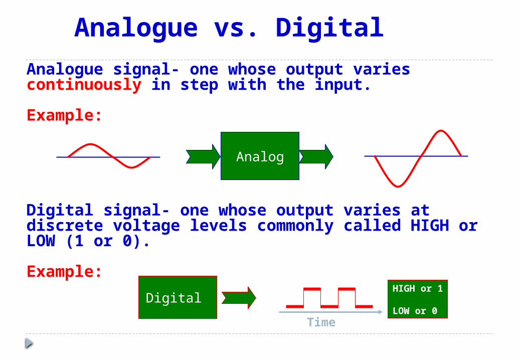
Analogue vs. DigitalAnalogue signal- one whose output varies continuously in step with the input.
Example:
Analog
Digital signal- one whose output varies at discrete voltage levels commonly called HIGH or LOW (1 or 0).
Example:
Digital HIGH or 1
LOW or 0Time

Why Digital?
Data can be stored (memory characteristic of digital). Data can be processed for error control and encryption. Compatible with display technologies. Compatible with computer technologies. Systems can be programmed. Digital IC families make design easier.

Why Analogue?
Most “real-world” events are analog in nature. Analogue processing is usually simpler. Analogue processing is usually faster. Traditional electronic systems were mostly analogue in
nature.

Defining Logic Levels
100%
90%
80%
70%
60%
50%
40%
30%
20%
10%
0%
HIGH
LOW
HIGH
LOW
Undefined
Undefined
TTLFamily of ICs
CMOSFamily of ICs
Vol
tage
• Logic devices interpret input voltages as either HIGH or LOW.• TTL or CMOS IC families have their unique voltage profiles.• TTl: +5V, CMOS: +12V, +9V or +5V.
CAUTION:Input voltages in the UNDEFINED region may yield unpredictable results.
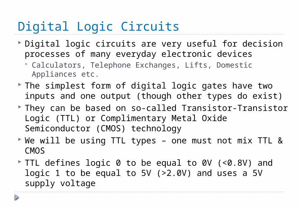
Digital Logic Circuits Digital logic circuits are very useful for decision processes of many
everyday electronic devices Calculators, Telephone Exchanges, Lifts, Domestic Appliances etc.
The simplest form of digital logic gates have two inputs and one output (though other types do exist)
They can be based on so-called Transistor-Transistor Logic (TTL) or Complimentary Metal Oxide Semiconductor (CMOS) technology
We will be using TTL types – one must not mix TTL & CMOS TTL defines logic 0 to be equal to 0V (<0.8V) and logic 1 to be
equal to 5V (>2.0V) and uses a 5V supply voltage

Different Logic Operators There are only a few types of basic logic operators
AND, OR, NAND, NOR, NOT, XOR and XNOR Each type has a specific circuit symbol (we shall see these later) The operation of each device is described by its “truth-table” Many devices can have more than two inputs but we will only
consider two input devices in this module The operations of the logic devices can be expressed
mathematically using “Boolean Algebra” Sometimes logic circuits are referred to as “gates” We will see each gate in turn…


AND Gate An “AND” gate has the following symbol and truth-table
It can be expressed using the following Boolean algebra
Sometimes you might see Q = A & B or the gate symbol may contain an “&” (ampersand)
A B Q
0 0 0
0 1 0
1 0 0
1 1 1
BAQ

NAND Gate A “NAND” gate has the following symbol and truth-table
It can be expressed using the following Boolean algebra
NOTE:
A B Q
0 0 1
0 1 1
1 0 1
1 1 0
BAQ
BABAQ

OR Gate An “OR” gate has the following symbol and truth-table
It can be expressed using the following Boolean algebra
A B Q
0 0 0
0 1 1
1 0 1
1 1 1
B A Q

NOR Gate A “NOR” gate has the following symbol and truth-table
It can be expressed using the following Boolean algebra
NOTE:
A B Q
0 0 1
0 1 0
1 0 0
1 1 0
B A Q
BAB A Q

NOT Gate A “NOT” gate has the following symbol and truth-table
It can be expressed using the following Boolean algebra
A NOT gate is sometimes referred to as an “inverter” “Schmitt Triggers” are specialised inverters with hysteresis
A Q
0 1
1 0
AQ

XOR Gate An “XOR” gate has the following symbol and truth-table
It can be expressed using the following Boolean algebra
NOTE:
A B Q
0 0 0
0 1 1
1 0 1
1 1 0
B A Q
BAB A Q

De Morgan’s Theorem De Morgan’s Theorem (or Law) states that a special
relationship exists between NOR and NAND operations such that
A B A+B
0 0 0 1 1 1 1 1 1
0 1 1 1 0 0 1 0 1
1 0 1 0 1 0 1 0 1
1 1 1 0 0 0 0 0 0
BABA and BABA
A B B.A A.B BA BA
NAND and NOR Gates It is a useful fact that all other types of logic functions can be
created from combinations of NAND gates or NOR gates Hence the NAND gate is the most commonly used gate In today’s experiment, you will be making other gate functions
using only NAND gates

Summary Basic Logic Gates TTL vs. CMOS Typical Gate Functions Boolean Algebra De Morgan’s Theorem Questions?

Principles of Computer Engineering:Lab Experiment 9: Basic TTL Logic

Introduction Introduction to TTL logic gates Use LEDs to indicate logic level Need to drive LEDs with inverters (NOT gates) Test four different combinations of NAND gates Extra “mystery” circuit to build and test Summary

TTL Logic Inputs The figure opposite shows how to
use resistors to apply logic 1 or logic 0 to standard TTL gate inputs
The 10kW resistor is acting as a pull-up resistor – when the switch closes the input voltage = 0V
The 470W resistor as a pull-down resistor – when the switch closes the input voltage = 5V
Logic 0 is defined as < 0.8V and Logic 1 as > 2.0 V
Important to be aware of losses
+ 1KΩ

Experiment Part 1: LED Indicators Most TTL logic gates are “open
collector” devices This means that they cannot provide
any source current They can only sink current Therefore to drive an LED we must
use inverse logic This means that logic 0 will activate
the LED and logic 1 will deactivate it Hence, we use inverters to drive the
LEDs to give true logic (make 3-off)
+

74LS04 (Hex NOT gate)
A Q LED
0 1 Off
1 0 On

Experiment: Part 2 Each circuit has two inputs and one output Use LED indicator circuits to show logic levels
+

74LS00 (Hex NAND gate)
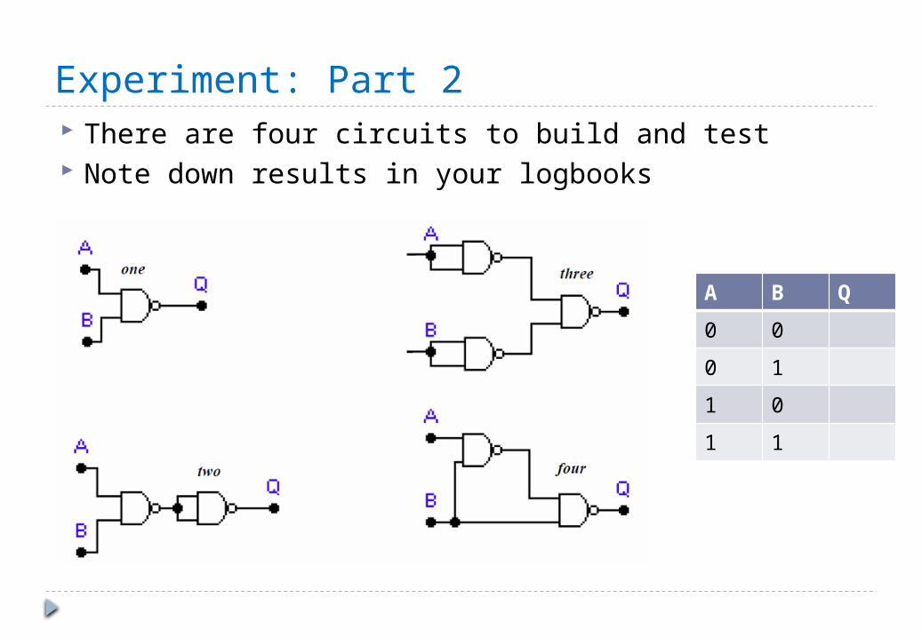
Experiment: Part 2 There are four circuits to build and test Note down results in your logbooks
+A B Q
0 0
0 1
1 0
1 1

Summary Build and test three LED indicator circuits using 74LS04
inverters Build and test the four circuits based on NAND gates Build and test the third “mystery” circuit based on NAND gates Any questions?