
preliminary design report gyropowerboard...
19
1 Gyro PowerBoard A gyroscopic single wheeled transportation device. Final Design Report EEL4924 – Electrical Engineering Design 2 April 19, 2014 Team Members: Sara Karimi, Jordan Williams PROJECT ABSTRACT For our project we built a single-wheel transportation device which combines the portability of a skateboard with the functionality of a Segway. The single-drive wheel is mounted directly in the center of the driver’s legs and the driver will ride facing laterally with respect to the motion of our device, as they would on a skateboard. A microprocessor is used to stabilize and facilitate automated motion, given gyroscopic and acceleration information collected from on-board sensors. The rider will tilt the board forward in order to increase his/her velocity, and tilt back to slow down, stop or even reverse direction. The main microprocessor output is fed to a motor drive control which contains a microcontroller used to generate the PWM signals for BLDC motor operation.
Transcript of preliminary design report gyropowerboard...
1
Gyro PowerBoard A gyroscopic single wheeled transportation device.
Final Design Report EEL4924 – Electrical Engineering Design 2
April 19, 2014
Team Members: Sara Karimi, Jordan Williams
PROJECT ABSTRACT
For our project we built a single-wheel transportation device which combines the
portability of a skateboard with the functionality of a Segway. The single-drive wheel is
mounted directly in the center of the driver’s legs and the driver will ride facing laterally
with respect to the motion of our device, as they would on a skateboard. A
microprocessor is used to stabilize and facilitate automated motion, given gyroscopic
and acceleration information collected from on-board sensors. The rider will tilt the
board forward in order to increase his/her velocity, and tilt back to slow down, stop or
even reverse direction. The main microprocessor output is fed to a motor drive control
which contains a microcontroller used to generate the PWM signals for BLDC motor
operation.

2
TABLE OF CONTENTS
page
LIST OF TABLES ............................................................................................................ 2
LIST OF FIGURES .......................................................................................................... 2
INTRODUCTION ............................................................................................................. 4
Project Features ....................................................................................................... 4
Analysis of Competitive Products: ............................................................................ 5
TECHNOLOGY SELECTION .......................................................................................... 6
IMPLEMENTATION METHODOLOGY ........................................................................... 8
Project Architecture .................................................................................................. 8 Bill of Materials ....................................................................................................... 16 Implementation Timeframe ..................................................................................... 17
REFERENCES .............................................................................................................. 19
LIST OF TABLES
Table page Table 3-1: Bill of Materials ............................................................................................. 16
Table 3-2: Major Activity List with Anticipated Start Date and Task Duration ................ 17
LIST OF FIGURES
Figure page Figure 3-1: Project Block Diagram .................................................................................. 9
Figure 3-2: Stabilization Schematic Diagram ................................................................ 10
Figure 3-3: Voltage Supply Regulation Schematic Diagram .......................................... 11
Figure 3-4: Motor Controller (Processor) Schematic Diagram ....................................... 12
Figure 3-5: Motor Controller (Drive) Schematic Diagram .............................................. 13
3
Figure 3-6: Motor Controller Software Flowchart ........................................................... 14
Figure 3-7: Stabilization Software Flowchart ................................................................. 15
Figure 4-2: Gantt chart of Anticipated Project and Activity Duration .............................. 18
4
CHAPTER 1
INTRODUCTION
Our board is intended for riders of all abilities for both leisure and short-distance
commuting purposes. To keep even the most inexperienced rider balanced on the
board, our device relies on gyroscopic stabilization via PID control. This will allow the
user to balance on the wheel axis when stationary and to remain balanced while
controlling the motor speed with their physical orientation.
Most electrically powered transportation systems in the market today are large
and bulky; our device will be a lightweight, portable alternative to these products. Other
similar solutions are currently being developed, but we hope to differentiate our product
in the future by integrating solar charging of the device by placing solar cells on the
deck of the board. In the future we are also considering developing a wireless hand-
held speed control which will allow the rider to continually vary his/her maximum
possible speed and which provides the rider with pertinent information such as his/her
current speed, remaining battery life and GPS location of the board.
Project Features
Although the project could be expanded to include many advanced features for
monitoring and improving general usability we have decided to limit the feature set to
only those required for basic functionality. We have designed the board in such a way
that these additional features could be easily added without changing the existing
circuitry or structure of the board.
The functional features applicable to the project at hand are as follows:
A vehicle with one wheel that provides a self-balancing surface to carry
a payload (in this case a rider).
5
The vehicle’s velocity must be controllable only by moving the deck of
the board.
The vehicle must mechanically contain all electronics batteries and
additional operational parts in order to maintain a clean deck for the
rider to stand.
The vehicle must be capable of steering with forces on the deck
perpendicular to the direction of motion
The vehicle must have a speed and battery life that is acceptable for
both indoor and outdoor operation.
The vehicle must be of a reasonable size and weight such that
transportation by hand is possible if necessary.
Analysis of Competitive Products:
Investigation of competitive products leads us to two major competitors. First and
in existence for the longest time is the Segway. It is a two wheeled balancing vehicle
where the rider faces parallel to the direction of motion. This product is heavy and is not
as portable as the Gyro PowerBoard. Until recently the only other products with a single
wheel like the Gyro PowerBoard were built by students and engineers and there were
only a handful in existence. The oldest one we could find was built in 2008.
Coincidently, during the course of construction of our product a company unveiled a
prototype and raised over $600,000 to begin construction of a commercial version of the
board. There advertised price was approximately $1700 per unit. The best advantage
of their product was its weight but there was a significant trade off with respect to
battery life.
6
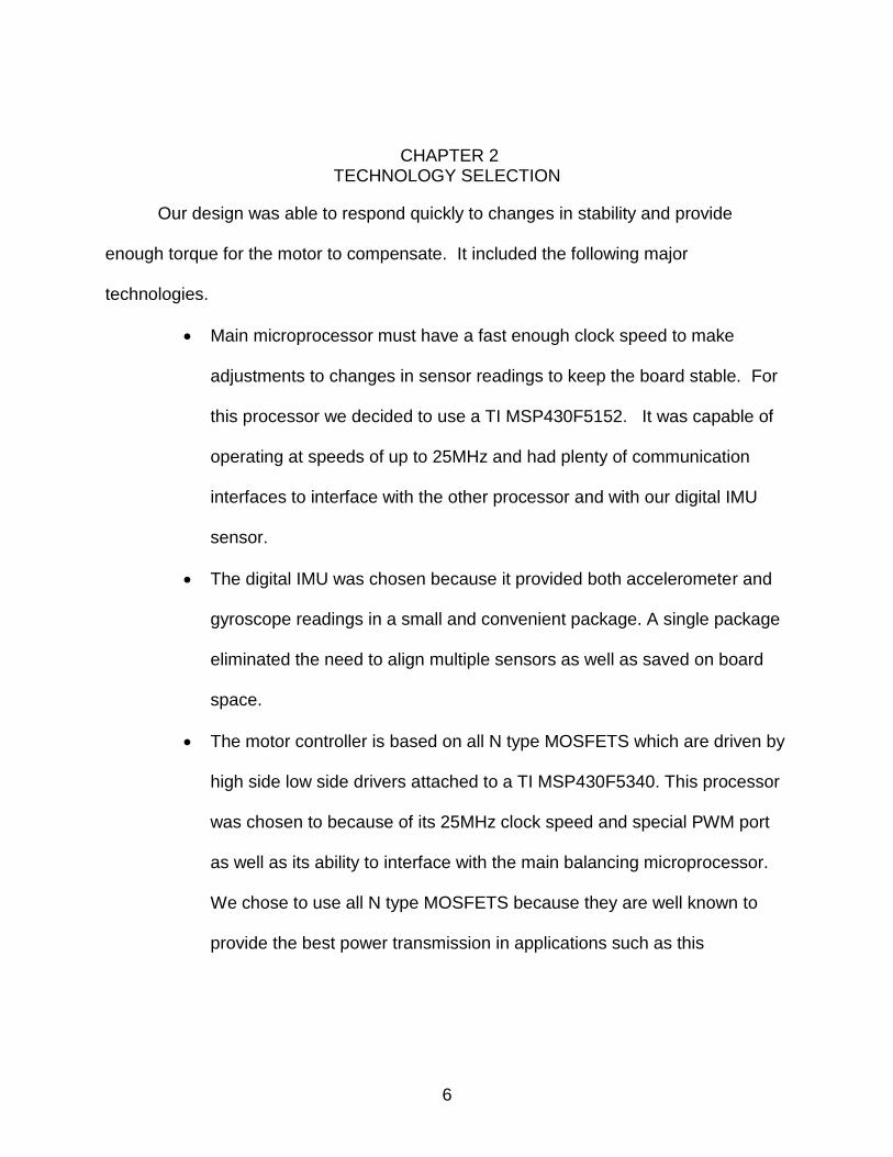
CHAPTER 2 TECHNOLOGY SELECTION
Our design was able to respond quickly to changes in stability and provide
enough torque for the motor to compensate. It included the following major
technologies.
Main microprocessor must have a fast enough clock speed to make
adjustments to changes in sensor readings to keep the board stable. For
this processor we decided to use a TI MSP430F5152. It was capable of
operating at speeds of up to 25MHz and had plenty of communication
interfaces to interface with the other processor and with our digital IMU
sensor.
The digital IMU was chosen because it provided both accelerometer and
gyroscope readings in a small and convenient package. A single package
eliminated the need to align multiple sensors as well as saved on board
space.
The motor controller is based on all N type MOSFETS which are driven by
high side low side drivers attached to a TI MSP430F5340. This processor
was chosen to because of its 25MHz clock speed and special PWM port
as well as its ability to interface with the main balancing microprocessor.
We chose to use all N type MOSFETS because they are well known to
provide the best power transmission in applications such as this

7
An aluminum frame was designed to provide a safe area to house all of
the electronics as well as a sufficient base to mount the mechanical
system while still remaining light enough to consider portable.
Energy storage is provided by 16 LiFePO4 battery cells, each with a
nominal voltage of 3.2V and capacity of 10Ah. The battery should provide
enough power for continued operation up to 40 minutes, although exact
capacities have yet to be determined. Low-voltage shut-off and over-
current protection circuitry should was added to ensure safe management
of the battery.
The motor selected was a 700 watt BLDC motor. It was designed for
automation applications but we felt it would work well for our application.

8
CHAPTER 3 IMPLEMENTATION METHODOLOGY
Project Architecture
The project was designed to have all of the electronics on 4 separate boards.
These electronics were intended to work together to facilitate the successful operation
of the vehicle. In addition to the electronics there are a few other systems in play which
allow the board to function.
The main controller board includes the digital IMU and the controller
microprocessor. The IMU takes gyro and accelerometer readings which are read by the
control microprocessor via SPI. With these readings the control microprocessor decides
on the appropriate torque and direction and sends them to the other side of the vehicle
where the motor control is listening via UART.
The motor controller board consists of high side low side drivers as well as 6 N
channel MOSFETS, a control processor and associated current sense circuitry. This
board is responsible for taking torque and direction commands from the controller and
commutating the motor accordingly. This processor also initiates electronic braking if it
is required to expeditiously change direction.
Both processors require 3.3V, the drivers 12V, the motor’s hall sensors require
5V and the actual drive voltage required on the motor is 48V. In order to make our
vehicle as stream lined as possible we created an independent power supply board to
be housed near the batteries. It is the responsibility of the circuitry on this board to step
down the battery voltage from 48V to the necessary levels which are then distributed
around the vehicle. The exception is the 48V power for the motor is delivered directly
from the BMS to the motor controller.

9
The fourth and final electronic system involved in the functionality of the Gyro
PowerBorad is the battery management system of BMS. This circuit monitors each cell
individually as well as the temperature of the pack and the charge and discharge
current. It waits for any irregularities and takes the batteries offline before something is
damaged.
Mechanically the motor uses a belt with a 4:1 reduction ratio to turn the wheel.
This gives us the appropriate mechanical advantage for a vehicle of this size. The wheel
is mounted on an axle in the center of the frame. A 12x7” pneumatic tire was chosen to
ensure the appropriate stability to turn ability ratio while still providing a smooth ride.
Figure 3-1: Project Block Diagram
As shown above in figure 4-1, the project consists of two main components—the
stabilization control and motor control. Communication between the two modules takes

10
place via UART. Schematic layouts of each component, in addition to the voltage
regulation system, are shown below.
Figure 3-2: Stabilization Schematic Diagram
NC1
NC2
NC3
NC4
NC5
NC6
AUX_CL7
VDDIO8
SDO/AD09
REGOUT10
FSYNC11
INT12
VDD
13NC
14NC
15NC
16NC
17GN
D18
RESV19
RESV20
AUX_DA21
nCS22
SCL/SCLK23
SDA/SDI24
IMU1
IMU
P1.0
/PM
_UCA
0CLK
/PM
_UCB
0STE
/A0*
/CB0
1P1
.1/P
M_U
CA0T
XD/P
M_U
CA0S
IMO/
A1*/
CB2
P1.2
/PM
_UCA
0RXD
/PM
_UCA
0SOM
I/A2*
/CB2
3P1
.3/P
M_U
CB0C
LK/P
M_U
CA0S
TE/A
3*/C
B34
P1.4
/PM
_UCB
0SIM
O/PM
_UCB
0SDA
/A4*
/CB4
5P1
.5/P
M_U
CB0S
OMI/P
M_U
CB0S
CL/A
5*/C
B56
PJ.0
/SM
CLK/
TDO/
CB6
7PJ
.1/M
CLK/
TDI/T
CLK/
CB7
8PJ
.2/A
DC10
CLK/
TMS/
CB8
9PJ
.3/A
CLK/
TCK/
CB9
10P1
.6/P
M_T
D0.0
11P1
.7/P
M_T
D0.1
12P2
.0/P
M_T
D0.2
13P2
.1/P
M_T
D1.0
14P2
.2/P
M_T
D1.1
15P2
.3/P
M_T
D1.2
16DV
IO17
DVSS
18P2
.4/P
M_T
EC0C
LR/P
M_T
EC0F
LT2/
PM_T
D0.0
19P2
.5/P
M_T
EC0F
LT0/
PM_T
D0.1
20P2
.6/P
M_T
EC0F
LT1/
PM_T
D0.2
21
P2.7
/PM
_TEC
1CLR
/PM
_TEC
1FLT
1/PM
_TD1
.022
P3.0
/PM
_TEC
1FLT
2/PM
_TD1
.123
P3.1
/PM
_TEC
1FLT
0/PM
_TD1
.224
VCOR
E25
DVSS
26
DVCC
27
PJ.6
/TD1
CLK/
TD0.
1/CB
1528
P3.2
/PM
_TD0
.0/P
M_S
MCL
K/CB
1429
P3.3
/PM
_TA0
CLK/
PM_C
BOUT
/CB1
330
P3.4
/PM
_TD0
CLK/
PM_M
CLK
31
TEST
/SBW
TCK
32
*RST
/NM
I/SBW
TDIO
33
P3.5
/PM
_TA0
.2/A
8*/V
REF+
*/CB
1234
P3.6
/PM
_TA0
.1/A
7*/V
REF-
*/CB
1135
P3.7
/PM
_TA0
.0/A
6*/C
B10
36
AVCC
37
PJ.4
/XOU
T38
PJ.5
/XIN
39
AVSS
40
EPAD
41
uP MSP
430F
5152
_RSB
_
.1u
C_IM
U_Vd
dCa
p2
3.3V
GND
GND
.1u
C_IM
U_re
gCa
p2
10n
C_IM
U_Vd
dio
Cap2
GND
GND
3.3V
GND
GND
GND
GND
3.3V
3.3V
3.3V 1
2
P_UA
RT_M
CHe
ader
2H
12
34
56
78
910
1112
1314
JTAG
_pro
g
Head
er 7
X2
GND
3.3V
10u
C2_J
TAG
Cap2
.1u
C3_J
TAG
Cap2
2.2n
C1_J
TAG
Cap2
47k
R1_J
TAG
Res1
GND
GND
GND
GND
3.3V
GND
11
22
powe
r
2pin
_con
necto
r
10u
C1_3
.3V
Cap2
.1u
C2_3
.3V
Cap2
GND
GND

11
Figure 3-3: Voltage Supply Regulation Schematic Diagram
10uF
Cin
_2
22uF
Cout_
2
620pF
Css
_2
L2
Rfb
1_2
Rfb
2_1
Rpg_2
EN
13
SS
/TR
9
GN
D15
FB5
DE
F8
FS
W7
SW1
VIN
11
VO
S14
PG
4
U2
27nF
Cboot_
1
1.8
nF
Cco
mp_1
22pF
Chf_
1
1uF
Cin
_1
22uF
Cout_
1
2.2
uF
Cout1
470pF
Cra
mp_1
2.2
uF
Crs
t_1
10nF
Css
_1
470nF
Cvcc
_1
790m
V
D1
27uH
L1
100V
M1
36.5
k
Rco
mp_1
1.9
1k
Rfb
b_1
16.9
k
Rfb
t_1
200k
Rra
mp_1
30m
Rsn
s_1
10.7
k
Rt_
1
2.6
1k
Ruv1
49.9
k
Ruv2
VIN1
EN
2
SS
3
RA
MP
4
RT
/SY
NC
5
GND6
COMP7
FB
8
OU
T9
RE
S/D
ITH
10
CS
G11
CS
12
SW
13
HG
14
BO
OT
15
VC
C16
LM
50
88
MH
X-1
/NO
PB
U1
Cin
_3
Cout_
3
Css
_3
L3
Rfb
1_3
Rfb
2_3
Rpg_3
EN
13
SS
/TR
9
GN
D15
FB5
DE
F8
FS
W7
SW1
VIN
11
VO
S14
PG
4
U3
11
22
33
44
mco
ntr
ol_
connec
t4pin
_co
nnec
tor
12V
5V
3.3
V
12V
5V
3.3
VG
ND
11
22
input_
connec
t2pin
_co
nnec
tor
11
22
stab
iliz
atio
n_co
nnec
t2pin
_co
nnec
tor
3.3
VG
ND
12
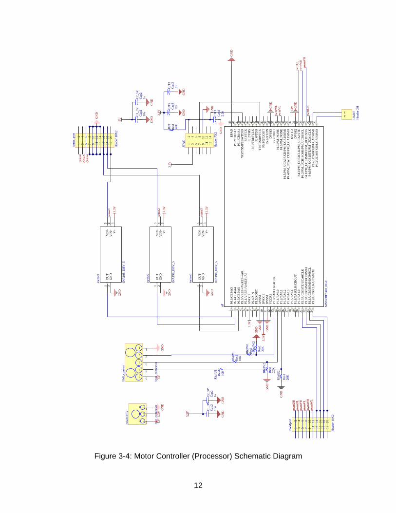
Figure 3-4: Motor Controller (Processor) Schematic Diagram
P6.3
/CB
3/A
31
P6.4
/CB
4/A
42
P6.5
/CB
5/A
53
P5.0
/VR
EF
+/V
eRE
F+
/A8
4
P5.1
/VR
EF
-/V
eRE
F-/
A9
5
AV
CC
16
P5.4
/XIN
7
P5.5
/XO
UT
8
AV
SS
19
DV
CC
110
DV
SS
111
VC
OR
E12
P1.0
/TA
0C
LK
/AC
LK
13
P1.1
/TA
0.0
14
P1.2
/TA
0.1
15
P1.3
/TA
0.2
16
P1.4
/TA
0.3
17
P1.5
/TA
0.4
18
P1.6
/TA
1C
LK
/CB
OU
T19
P1.7
/TA
1.0
20
P2.7
/UC
B0S
TE
/UC
A0C
LK
21
P3.0
/UC
B0S
IMO
/UC
B0S
DA
22
P3.1
/UC
B0S
OM
I/U
CB
0S
CL
23
P3.2
/UC
B0C
LK
/UC
A0S
TE
24
P3.3
/UC
A0T
XD
/UC
A0S
IMO
25
P3.4
/UC
A0R
XD
/UC
A0S
OM
I26
P4.0
/PM
_U
CB
1S
TE
/PM
_U
CA
1C
LK
27
P4.1
/PM
_U
CB
1S
IMO
/PM
_U
CB
1S
DA
28
P4.2
/PM
_U
CB
1S
OM
I/P
M_U
CB
1S
CL
29
P4.3
/PM
_U
CB
1C
LK
/PM
_U
CA
1S
TE
30
DV
SS
231
DV
CC
232
P4.4
/PM
_U
CA
1T
XD
/PM
_U
CA
1S
IMO
33
P4.5
/PM
_U
CA
1R
XD
/PM
_U
CA
1S
OM
I34
P4.6
/PM
_N
ON
E35
P4.7
/PM
_N
ON
E36
P5.7
/TB
0.1
37
DV
SS
338
P5.2
/XT
2IN
39
P5.3
/XT
2O
UT
40
TE
ST
/SB
WT
CK
41
PJ.
0/T
DO
42
PJ.
1/T
DI/
TC
LK
43
PJ.
2/T
MS
44
PJ.
3/T
CK
45
*R
ST
/NM
I/S
BW
TD
IO46
P6.1
/CB
1/A
147
P6.2
/CB
2/A
248
EP
AD
49
uP
MS
P430F
5340_R
GZ
12
34
56
78
910
11
12
13
14
JTA
G
Hea
der
7X
2
47k
RJT
Res
1.1
u
CJT
3C
ap2
10u
CJT
2C
ap2
2.2
n
CJT
1C
ap2GN
D
GN
D
GN
DG
ND
3.3
V
3.3
V
GN
D
GN
D
3.3
VGN
DG
ND
3.3
V
3.3
V
11
22
33
44
55
Hal
l_co
nn
ect
5pin
_co
nnec
tor
5V
GN
D
12
UA
RT
Hea
der
2H
20K
Rhal
U2
Res
1
20K
Rhal
V2
Res
1
20K
Rhal
W2
Res
1
10K
Rhal
U1
Res
1
10K
Rhal
V1
Res
1
10K
Rhal
W1
Res
1
GN
D
GN
D
GN
D
GN
D
10u
C1_5V
Cap
21u
C2_5V
Cap
2
5V
GN
DG
ND
11
22
33
pow
er3/5
V
3pin
_co
nnec
tor
OU
T1
GN
D2
V+
3V
IN+
4V
IN-
5
isen
se1
INA
19
8_
DB
V_
5
3.3
V
GN
D
OU
T1
GN
D2
V+
3V
IN+
4V
IN-
5
isen
se2
INA
19
8_
DB
V_
5
OU
T1
GN
D2
V+
3V
IN+
4V
IN-
5
isen
se3
INA
19
8_
DB
V_
5
3.3
V
3.3
V
GN
D
GN
D
12
34
56
78
910
11
12
13
14
15
16
17
18
19
20
PW
Mport
Hea
der
10X
2
12
34
56
78
910
11
12
13
14
15
16
17
18
19
20
isen
se_port
Hea
der
10X
2
5V
3.3
VG
ND
10u
C1_3V
Cap
21u
C2_3V
Cap
2
3.3
V
GN
DG
ND
pw
mU
H
pw
mU
Hpw
mV
Hpw
mW
Hpw
mU
L
pw
mW
Lpw
mV
L
pw
mV
H
pw
mW
H
pw
mU
L
pw
mW
L
pw
mV
L
sense1
sense2
sense3
sense
1
sense
2
sense
3
GN
D

13
Figure 3-5: Motor Controller (Drive) Schematic Diagram
VDD1
HB2
HO3
HS4
HI5
LI6
VSS7
LO8
EPADEPAD
Drv_U
UCC27210_DDA_8
VDD1
HB2
HO3
HS4
HI5
LI6
VSS7
LO8
EPADEPAD
Drv_V
UCC27210_DDA_8
VDD1
HB2
HO3
HS4
HI5
LI6
VSS7
LO8
EPADEPAD
Drv_W
UCC27210_DDA_8
100
Rg_ULs
Res1
1K
Rg_ULpRes1
100
RgVLs
Res1
1K
RgVLpRes1
1K
RgWLs
Res1
1K
RgWLpRes1
1K
RgUHs
Res1
1K
RgUHpRes1
100
RgVHs
Res1
1K
RgVHpRes1
1K
RgWHs
Res1
1K
RgWHpRes1
GND
48V
48V
48V
12V
12V
12V
.1u
CU1Cap2
10u
CU2Cap2
GND GND
.1u
CV1Cap2
10u
CV2Cap2
.1u
CW1Cap2
10u
CW2Cap2
GND
GND
GND
GND
GND
11
22
11
22
shunt1shunt_resistor
GND_48V
po
wer
po
wer
gn
dg
nd
48Vpower
2pin_molex_50A_sch48V
GND_48V
WW
VV
UU
motor
3pin_molex_50A_sch
11
22
33
44
55
6677
88
di_VW
TI_PDIP8_diode
11
22
33
44
55
6677
88
di_UV
TI_PDIP8_diode
10u
CbsUCap2
10u
CbsWCap2
10u
CbsVCap2
220u
C1_48VCap
220u
C2_48VCap
GND_48V
11
22
11
22
shunt2shunt_resistor
11
22
11
22
shunt3shunt_resistor
GND_48V
GND_48V
1 23 45 67 89 1011 1213 1415 1617 1819 20
isense_port
Header 10X2
1 23 45 67 89 1011 1213 1415 1617 1819 20
PWMport
Header 10X2
11
22
power12V
2pin_connector
GND12V
sense1sense2sense3
sense1
sense2
sense3
D
G
S
fetUHE3_heatsink
D
G
S
fetULE3_heatsink
D
G
S
fetVHE3_heatsink
D
G
S
fetVLE3_heatsink
D
G
S
fetWHE3_heatsink
D
G
S
fetWLE3_heatsink
14
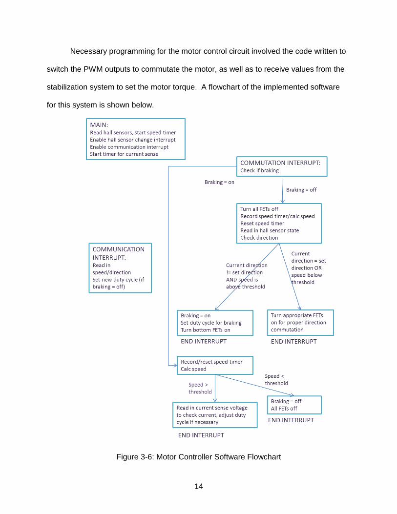
Necessary programming for the motor control circuit involved the code written to
switch the PWM outputs to commutate the motor, as well as to receive values from the
stabilization system to set the motor torque. A flowchart of the implemented software
for this system is shown below.
Figure 3-6: Motor Controller Software Flowchart
15
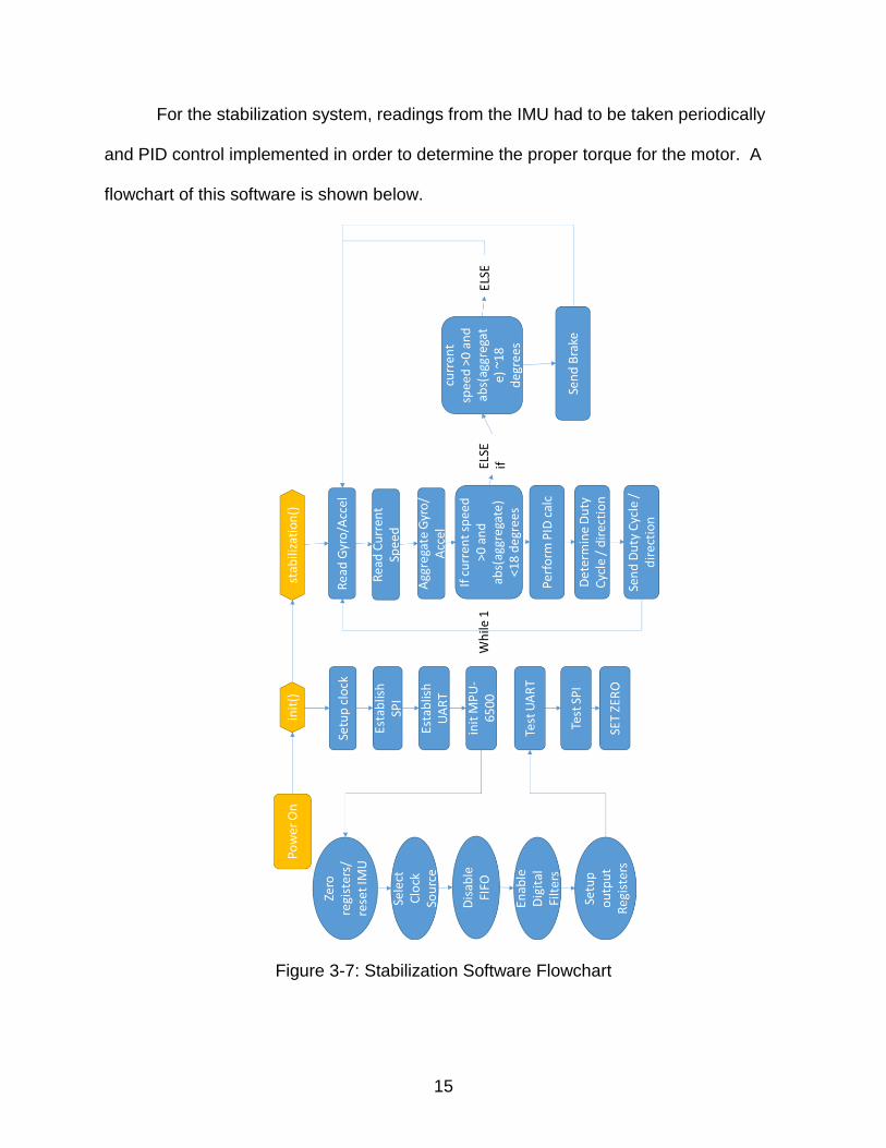
For the stabilization system, readings from the IMU had to be taken periodically
and PID control implemented in order to determine the proper torque for the motor. A
flowchart of this software is shown below.
Figure 3-7: Stabilization Software Flowchart

16
Bill of Materials
Table 3-1: Bill of Materials
Item Price
MSP430F5152 (uP) $3.00
MSP430F5340 (uP) $4.00
MPU-6500 (IMU) $12.00
LM5088 (Buck Converter) $4.00
TPS62140RGTR (Buck
Converter)
(2)$3.00
Miscellaneous passive
electronic components
$150.00
PCB Manufacturing $200.00
Aluminum Frame $250.00
Wheel and tire $70.00
BLDC 700 watt Motor $120.00
Drive components $150.00
Batteries $400.00
Battery Charger $70.00
Miscellaneous hardware $60.00
INA98 (Current Shunt Monitor) (3) $2.00
UCC27211 (Driver) (3) $2.00
CSD19531KCS(MOSFET) (6) $5.00
Total (EST) $1,541.00
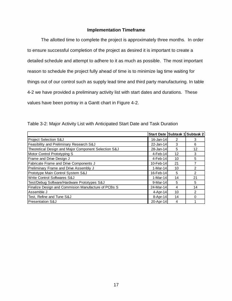
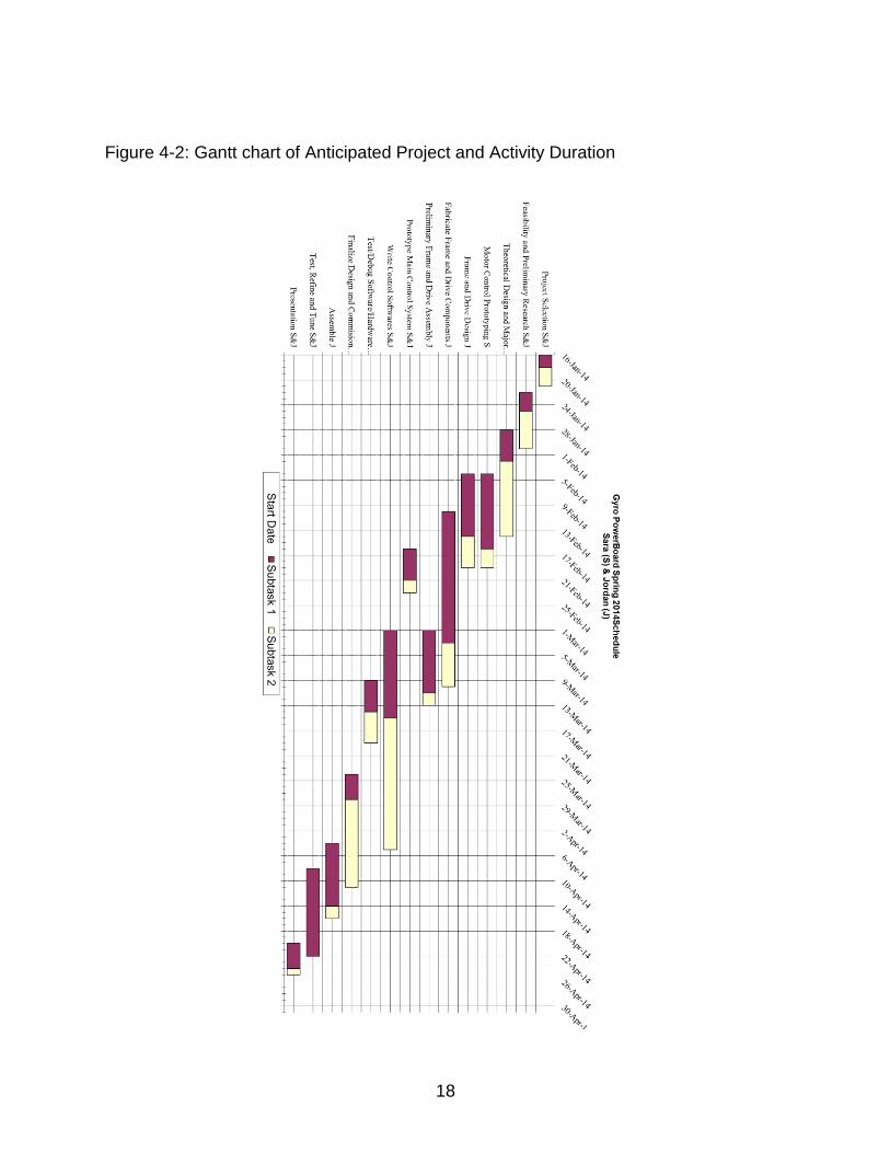
17
Implementation Timeframe
The allotted time to complete the project is approximately three months. In order
to ensure successful completion of the project as desired it is important to create a
detailed schedule and attempt to adhere to it as much as possible. The most important
reason to schedule the project fully ahead of time is to minimize lag time waiting for
things out of our control such as supply lead time and third party manufacturing. In table
4-2 we have provided a preliminary activity list with start dates and durations. These
values have been portray in a Gantt chart in Figure 4-2.
Table 3-2: Major Activity List with Anticipated Start Date and Task Duration
Start Date Subtask 1 Subtask 2
Project Selection S&J 16-Jan-14 2 3
Feasibility and Preliminary Research S&J 22-Jan-14 3 6
Theoretical Design and Major Component Selection S&J 28-Jan-14 5 12
Motor Control Prototyping S 4-Feb-14 12 3
Frame and Drive Design J 4-Feb-14 10 5
Fabricate Frame and Drive Components J 10-Feb-14 21 7
Preliminary Frame and Drive Assembly J 1-Mar-14 10 2
Prototype Main Control System S&J 16-Feb-14 5 2
Write Control Softwares S&J 1-Mar-14 14 21
Test/Debug Software/Hardware Prototypes S&J 9-Mar-14 5 5
Finalize Design and Commision Manufacture of PCBs S 24-Mar-14 4 14
Assemble J 4-Apr-14 10 2
Test, Refine and Tune S&J 8-Apr-14 14 0
Presentation S&J 20-Apr-14 4 1
18
Figure 4-2: Gantt chart of Anticipated Project and Activity Duration

19
CHAPTER 4 REFERENCES
http://sites.google.com/site/gyropowerboard


![f a reassembled PDU] - Texas Instrumentse2e.ti.com/cfs-file/__key/communityserver-discussions-components... · 2050 86.673954000 192.168.1.103 192.168.1.100 ... [TCP segment o f a](https://static.fdocuments.us/doc/165x107/5b05c4e67f8b9a93418bcf7a/f-a-reassembled-pdu-texas-86673954000-1921681103-1921681100-tcp-segment.jpg)


