
“Predicting Circuit ESD Performance Through SPICE-type...
48
The World Leader in High Performance Signal Processing Solutions Proprietary Information Proprietary Information “Predicting Circuit ESD Performance Through SPICE-type Simulations” Yuanzhong (Paul) Zhou, Thorsten Weyl & Jean-Jacques (J-J) Hajjar Analog Devices Inc. IEEE Electron Device Colloquium University of Central Florida February 21-22, 2008
Transcript of “Predicting Circuit ESD Performance Through SPICE-type...

The World Leader in High Performance Signal Processing Solutions
Proprietary InformationProprietary Information
“Predicting Circuit ESD Performance Through SPICE-type Simulations”
Yuanzhong (Paul) Zhou,Thorsten Weyl &
Jean-Jacques (J-J) Hajjar
Analog Devices Inc.
IEEE Electron Device ColloquiumUniversity of Central Florida
February 21-22, 2008

2 —Analog Devices Proprietary Information—
ESD high on Pareto chart of reliability product returns from customers
Predicting ESD performance is very compelling:1) Design tool prior to manufacturing
2) Design verification
3) Post-mortem failure troubleshooting tool
MOTIVATION

3 —Analog Devices Proprietary Information—
What is ESD?
Circuit Simulation Consideration
Compact Modeling Approaches and Modeling Verification
ESD Circuit Simulation Examples
Concluding Remarks
OUTLINE
4 —Analog Devices Proprietary Information—
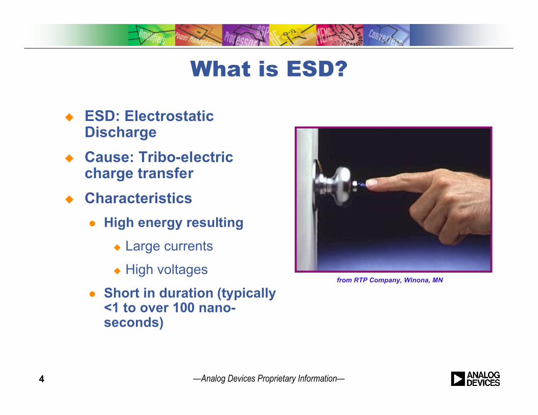
ESD: Electrostatic Discharge
Cause: Tribo-electric charge transfer
Characteristics
High energy resulting
Large currents
High voltages
Short in duration (typically <1 to over 100 nano-seconds)
What is ESD?
from RTP Company, Winona, MN

5 —Analog Devices Proprietary Information—
SOURCE of ESDi_hbm_0 i_mm_0 i_cdm_4pf
-4
-3
-2
-1
0
1
2
3
4
5
6
7
8
0 5 10 15 20 25 30 35 40 45 50 55 60 65 70time, x1e-9 Seconds
Human touches IC: Human Body Model (HBM)
Charged IC touches grounded surface: Charged Device Model (CDM)
Charged machine touches IC: Machine Model (MM)
10-10 10-410-6 10-5 10-3 10-2 10-1 10010-9 10-8 10-7
EOS
ESD
TIME in SECONDS (LOG SCALE)
HBM(0.3-3 Amp)
MM(2-10 Amp)
"Typical" EOS(0.1-10 Amp)
CDM(3-15 Amp)
DC EOS(0.1-10+Amp)

6 —Analog Devices Proprietary Information—
ESD DAMAGE in ICs (1)MOSFET Gate-Oxide Punch-through
• SEM micrograph depicts NMOS after de-processing.
• Pits are 0.2 to 0.5m in width & correspond to regions where Si flowed into gate oxide.
DRAINCHANNELSOURCE
Channel
Drain
Source
N+DRAINN+SOURCE
POLY
PSUB
STI STI
GATE OXIDE
METAL
GATE OXIDE DAMAGE

7 —Analog Devices Proprietary Information—
ESD DAMAGE in ICs (2)Junction Damage/Contact Spiking
• SEM micrograph depicts NMOS after de-processing.
DRAIN-CHANNELJUNCTION DAMAGE
DRAINCONTACTSPIKING
DRAINCHANNELSOURCE
N+SOURCE
POLY
PSUB
STI STI
GATE OXIDE
METAL
DRAIN CONTACTSPIKING
DRAIN-CHANNELJUNCTION DAMAGE
N+DRAIN

8 —Analog Devices Proprietary Information—
OBJECTIVE:1. Shunt current
discharges awayfrom the CORE CIRCUIT
2. Clamps I/O & Power pad voltage to a safe level
On-Chip ESD PROTECTION SCHEMES
IN OUT
VDD
VSS
CORE CIRCUITE
SD
ES
D
ES
D
ES
DE
SD
VDDVSS

9 —Analog Devices Proprietary Information—
IN OUT
VDD
VSS
CORE CIRCUIT
On-Chip ESD PROTECTION SCHEMESAn Example

10 —Analog Devices Proprietary Information—
Circuit Simulation Considerations
Impact of ESD structure on I/O and core circuits.
ESD current paths.
Impact of internal circuitry on ESD protection performance.
Optimization to reduce ESD over design.

11 —Analog Devices Proprietary Information—
Circuit Simulation Approach
SPICE is a Primary Tool for Circuit Level Simulation
ESD–capable Compact Device model
Modeling physical phenomenon particular to ESD:
Breakdown
Snapback
…

12 —Analog Devices Proprietary Information—
Major Challenges (1)
Devices operate in unintended bias space:
high voltages
very large currents
VOLTAGE
CU
RR
EN
T
DEVICE FAILURE
INTENDED OPERATION
AVALANCE CURRENT (VMAX, IMAX)
0
MOSFET CHARACTERISTICS

13 —Analog Devices Proprietary Information—
Major Challenges (2)
Device operation highly dependent on layout. ESD NMOS – DESIGN SPACE
Width Gate length w/ or w/o RPO in drain Drain side CTP Gate stripes Substrate contact
CONT
NSD
WF
NF=2
RPO
SUBST
CONT-TO-POLY (CTP)
POLY
ESD NMOS

14 —Analog Devices Proprietary Information—
Major Challenges (3)
Thermal effects important
Parasitics (L, C & R) critical due to fast-transient nature of ESD: Interconnect Package Board Test fixture …

15 —Analog Devices Proprietary Information—
What Devices to Model?
Primary Protection Devices1) MOS2) SCR3) Bipolar4) Diodes5) Resistors
Modeling Strategy1) Modify standard Compact models2) Customized Model

16 —Analog Devices Proprietary Information—
Snapback in ESD Devices
Operating I-V Regions of MOS Devices1) Linear Region2) Saturation Region3) Avalanche Region 4) Snapback Region5) Failure Region
Vt1 represents the “snapback effect”trigger voltage
Devices (MOS) operating in “snapback” mode carries more current per unit width
VDRAIN
I DR
AIN
DEVICE
REGION-1
0
REGION-2
REGION-3
REGION-4
GATE BIAS
Vt1
REGION-5
FAILS

17 —Analog Devices Proprietary Information—
Snapback Effect in MOS is due to the Parasitic BJT, triggered by the substrate current (ISUB).
Snapback in MOS Devices
N+N+P+
POLY
VS
VG
VD
PSUB
STI STISTI
ISUB
N+N+P+
POLY
VS
VG
VD
PSUB
STI STISTI
RSUB
LNPN
IC
ISD
ISUB

18 —Analog Devices Proprietary Information—
Substrate current as function of VDS, VGS
and VBS
Due to impact ionization in Drain/Backgatedepletion layer.
Avalanche current multiplication factor is different before and after snapback
Displacement current (dV/dt) through Drain/Backgate junction
Gate induced drain leakage (GIDL)
Critical Effects in Snapback Modeling

19 —Analog Devices Proprietary Information—
Standard MOS and BJT models.
An explicit current source which is a function of VGSand VDS
(dV/dt) effect, GIDL and separate M for MOS and BJT are included in some models by adding equations.
The implementation of the models includes C code and behavioral languages (Verilog-A)
Previous Snapback Models
G
DS
B
RdRs
Rsub
Igen
Ic
Ids
Id=Ids+Ic+Igen
Isub
Ib

20 —Analog Devices Proprietary Information—
Model for MOS under ESD Stress
New approach eliminates the current source of previous models.
Model constructed of standard BJT (Mextram) and MOS (BSIM4) devices.
Models intrinsically includes all major physical phenomenon presented.
Source/Backgate and Drain/Backgate Junction Diodes for completeness.
G
BSIM4Mextram
Ib
BiIsub_total
Rsub
Isub+Igidl
Id=Id'+Ic
Ic
Ids
Id'
S
D
B
S/B diode
D/B diode

21 —Analog Devices Proprietary Information—
Model Verification
Transmission Line Pulse measurement:
Quasi-static
Transient

22 —Analog Devices Proprietary Information—
Transmission Line Pulse (TLP)Measurement Setup
+-
High voltage supply
Transmission Line; Z0 = 50
DUT
Termination
VDUT (t)
IDUT (t)
Current Probe
100 ns
t rise
VTLP
ITLP
VTLP
ITLP
ZT1
ZT2 ZATT
.......
time
I

23 —Analog Devices Proprietary Information—
Why Transmission Line Pulse?
0
1
2
0 100 200TIME (nsec)
CURRENT (A)
2,000V HBM
TLP

24 —Analog Devices Proprietary Information—
Model Verification Snapback effect was simulated with transient simulation. Voltage Pulse Sequence (100ns) were used as the Input. The stabilized VD and ID were measured as the simulation
results (~80ns).
Schematic of Snapback Simulation(R=0 for ggNMOS)Voltage
source
50
R
TLP DUT
ID
VD
VHD

25 —Analog Devices Proprietary Information—
Simulation Results vs. TLP MeasurementA ggNMOS device
50
Id Vd GGNMOS Configuration

26 —Analog Devices Proprietary Information—
Deep submicron CMOS Model Scalability
W = 300m 0.18 < L < 0.30 m Stripes = 12 Wrap-around backgate contact
0
0.2
0.4
0.6
0.8
1
0 1 2 3 4 5 6 7 8VOLTAGE (V)
0
0.2
0.4
0.6
0.8
10
0.2
0.4
0.6
0.8
1 CURRENT (A)
L=0.18m
L=0.30m
L=0.20m
VB3
VB2
VB1
MOS CHARACTERISTICS & MODEL
G
S
D
BG
GGNMOS

27 —Analog Devices Proprietary Information—
0
0.2
0.4
0.6
0.8
1
0 1 2 3 4 5 6 7 8VOLTAGE (V)
0
0.2
0.4
0.6
0.8
1 CURRENT (A)
GCNMOSR=10k
GGNMOSR=0
VB2
VB1
Deep submicron CMOS W/L = 300/0.18m; Stripes = 12
GGNMOS GCNMOS
100ns TLP: Sim vs. msmt
MOS CHARACTERISTICS & MODEL
R=10k G
S
D
BGG
S
D
BG

28 —Analog Devices Proprietary Information—
SCR Devices
N+ P+ P+
Nwell
Rnwell Pwell
Rpwell
CATHODE ANODE
N+
Rnwell
Rpwell
npn
pnp
CATHODE
ANODE
N+ N+ N+ P+ P+
Nwell
Rnwell Pwell
Rpwell
CATHODE ANODE
Rnwell
Rpwell
npn
pnpnmos
CATHODE
ANODE
SCR LVTSCR

29 —Analog Devices Proprietary Information—
Macro Model for LVTSCR Similar approach to MOS New model consists of four components: An NMOS modeled by BSIM4 A four terminal NPN modeled by Mextram Two resistors
BSIM4
MEXTRAM

30 —Analog Devices Proprietary Information—
Key effects in New LVTSCR Macro Model
The PNP is modeled by the parasitic BJT in the 4 terminal NPN modeled by a Mextram-like model
Current sources for avalanche and GIDL are intrinsically built in MOS and BJT models
Decoupled multiplication factors for BJT and MOS are included in IAVL and ISUB respectively
The dV/dt effect is modeled by Collector/Base junction capacitance of the BJT
IGEN = IAVL + ISUB + IGIDL

31 —Analog Devices Proprietary Information—
CMOS: SCR-1
100nsec TLP Pulse Different pulse rise-time
SCR CHARACTERISTICS & MODEL
VDUT (t)
IDUT (t)
100 ns
t rise VTLP
ITLP
0
0.2
0.4
0.6
0.8
1.0
1.2
0 1 2 3 4 5 6 7 8VOLTAGE (V)
0
0.2
0.4
0.6
0.8
1.0
1.2
0
0.2
0.4
0.6
0.8
1.0
1.2
=10nsec.
=2nsec.
=0.2nsec.
VB1
VB2
VB3
CURRENT (A)

32 —Analog Devices Proprietary Information—
-5
0
5
10
15
20
25
0
10
20
30
40
0 1 2 3 4 5 6 7 8TIME (nsec.)
CU
RR
EN
T(A
)V
OL
TA
GE
(V)
SIMULATED
MEASURED
SCR CHARACTERISTICS & MODEL
CMOS: SCR-1
VFTLP: SCR ADICE Simulation vs. measurement

33 —Analog Devices Proprietary Information—
CIRCUIT SIMULATIONHuman Body Model (HBM)
Simulates the discharge from the finger of a standing person
IPEAK = ~0.67 A/kV, tRISE ~ 5-9ns, tDELAY = ~150 nsec.
Modeled by a Lumped Element Model (LEM)
S
DUTCESD=100pF Ct=10pFVHBM
Ls=7.5H
Cs=1pF
RHB=1500100%
90%
10%
CU
RR
EN
T
TIME
36.8%
tRISE tDELAY
HBM
LEM

34 —Analog Devices Proprietary Information—
SPICE Simulation ExamplesI/O Cell – Circuit
VSS
IA
VDD
RCTimer
D1
D2
MP0
MN0
R ?
TGATE
MN1

35 —Analog Devices Proprietary Information—
SPICE Simulation ExamplesI/O Cell – Simulation
WPMOS~2WNMOS
-400
-300
-200
-100
0
100
200
300
400
0 20 40 60 80 100 120 140 160
time, 10-9 sec.
Current (10-3 Amp)
MP0 - R=5
MN0 - R=5
MN0 - R=0
FAILURE REGION
FAILURE REGION
MP0 - R=0

36 —Analog Devices Proprietary Information—
SPICE Simulation ExamplesBlock Level
IAIB
VDD
VSSInternal Circuit
ES
D
ES
DE
SD
Sw
itch
1_B
ank_
0
Sw
itch
1_B
ank_
31
Sw
itch
2_B
ank_
0
Sw
itch
2_B
ank_
19

37 —Analog Devices Proprietary Information—
SPICE Simulation ExamplesBlock Level – Original Design Fails 1,000V HBM
IA
IB
VDD
VDD 51 x PMOS BANKS
Internal Circuit
Idmp3
Sub
Cel
l
Idmp5
VDD

38 —Analog Devices Proprietary Information—
SPICE Simulation ExamplesBlock Level – Simulation Results – Fails 1,000V
0
1
2
3
4
5
100 140 180 220 260 300
MP5
MP3
CURRENT DENSITY (mA/m)
TIME (nsec.)

39 —Analog Devices Proprietary Information—
SPICE Simulation ExamplesBlock Level – Revised Design Passes 1,500V HBM
IA
IB
VDD
VDD51 x PMOS BANKS
Internal Circuit
Idmp3
Sub
Cel
l
Idmp5
VDDClamp

40 —Analog Devices Proprietary Information—
SPICE Simulation ExamplesBlock Level – Simulation Results
41 —Analog Devices Proprietary Information—
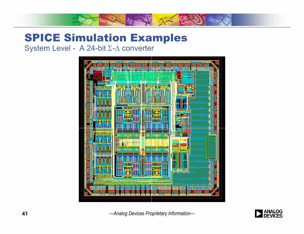
SPICE Simulation ExamplesSystem Level - A 24-bit - converter

42 —Analog Devices Proprietary Information—
SPICE Simulation ExamplesSystem Level - HBM Stress between VDD1 and VDD2
ESD ESD
ESD_GND
43 —Analog Devices Proprietary Information—
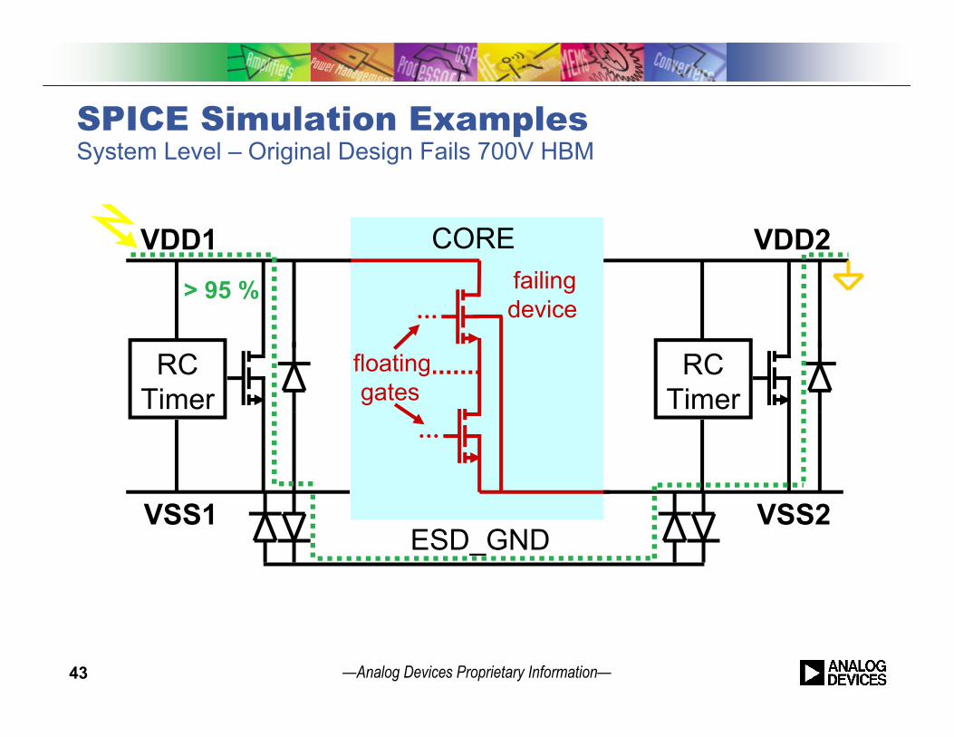
SPICE Simulation ExamplesSystem Level – Original Design Fails 700V HBM
failingdevice
floating gates
ESD_GND
VDD1
VSS1
RCTimer
VDD2
VSS2
RCTimer
> 95 %
CORE

44 —Analog Devices Proprietary Information—
SPICE Simulation ExamplesSystem Level – Simulation Highlights Core Circuitry Failure.
0
0.2
0.4
0.6
0.8
1.0
1.2
1.4
0
2
4
6
8
0 20 40 60 80 100 120 140 160
time, 10-9 sec.
10
-3
Current (Amp)
HBM=750V
PROTECTION DEVICE
FAILING CORE DEVICE
45 —Analog Devices Proprietary Information—
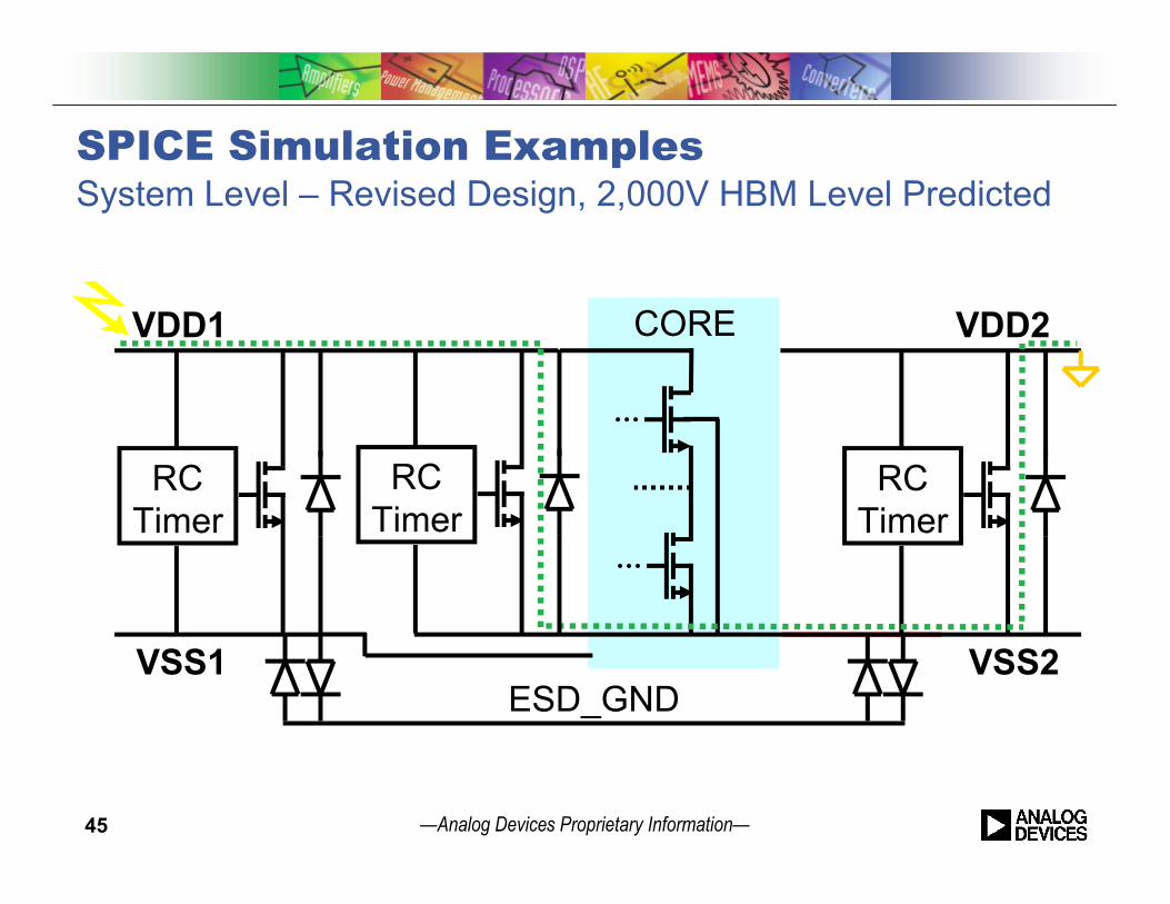
SPICE Simulation ExamplesSystem Level – Revised Design, 2,000V HBM Level Predicted
ESD_GND
VDD1
VSS1
RCTimer
VDD2
VSS2
RCTimer
CORE
RCTimer

46 —Analog Devices Proprietary Information—
SPICE Simulation ExamplesSystem Level – Simulation predicts failure above 2,000V HBM
0
0.2
0.4
0.6
0.8
1.0
1.2
0
2
4
6
8
0 20 40 60 80 100 120 140 160
10
-3HBM=2,000V
PROTECTION DEVICE
FAILING CORE DEVICE
time, 10-9 sec.
Current (Amp)

47 —Analog Devices Proprietary Information—
ESD is an important product reliability concern.
Compact Modeling approach for accurate modeling of MOS & SCR devices Uses Industry standard Models Simple Implementation
Successful SPICE-type circuit simulation of ESD event: Design ESD Protection Cells Predict ESD Performance Confirm and fix known ESD failures
SUMMARY

48 —Analog Devices Proprietary Information—
END