Practical identification of dispersive dielectric … identification of dispersive dielectric models...
24
DesignCon 2010 Practical identification of dispersive dielectric models with generalized modal S-parameters for analysis of interconnects in 6- 100 Gb/s applications Yuriy Shlepnev, Simberian Inc. [email protected] , +1-702-876-2882 Alfred Neves, Teraspeed Consulting Group [email protected] , + 1-503-718-7172 Tom Dagostino, Teraspeed Consulting Group [email protected] , +1-503-430-1065 Scott McMorrow, Teraspeed Consulting Group [email protected] , +1- (401) 284-1827 1
Transcript of Practical identification of dispersive dielectric … identification of dispersive dielectric models...
DesignCon 2010
Practical identification of dispersive dielectric models with generalized modal S-parameters for analysis of interconnects in 6-100 Gb/s applications Yuriy Shlepnev, Simberian Inc. [email protected], +1-702-876-2882 Alfred Neves, Teraspeed Consulting Group [email protected], + 1-503-718-7172 Tom Dagostino, Teraspeed Consulting Group [email protected], +1-503-430-1065 Scott McMorrow, Teraspeed Consulting Group [email protected], +1- (401) 284-1827
1
Abstract A novel method for extraction of dispersive dielectric parameters to 50 GHz is proposed. The method doesn’t require advanced de-embedding, and is based on correlation of measured and simulated generalized modal S-parameters of a line segment. First, VNA measurements for two line segments are made and used to compute generalized S-parameters of a difference segment. Second, 3D full-wave model of the difference segment with conductor model with roughness is used to identify the dielectric properties. We finalize the paper with the derivation of dielectric models for low-cost FR4-type and for expensive low-loss high-frequency materials. The advanced models can be used for practical electromagnetic analysis of interconnects for the 6-100 Gb/s realm. Authors Biographies Yuriy Shlepnev is the president and founder of Simberian Inc., were he develops electromagnetic software for advanced analysis of interconnects. He received M.S. degree in radio engineering from Novosibirsk State Technical University in 1983, and the Ph.D. degree in computational electromagnetics from Siberian State University of Telecommunications and Informatics in 1990. He was principal developer of a planar 3D electromagnetic simulator for Eagleware Corporation and leading developer of electromagnetic software for simulation of high-speed digital circuits at Mentor Graphics. The results of his research are published in multiple papers and conference proceedings. Alfred Neves is a Senior Staff Signal Integrity Engineer working with Teraspeed Consulting LLC. He received BSEE degree in Mathematics from University of Massachusetts. He has worked in the Signal integrity field for 13 years focusing on backplane design, advanced jitter analysis, practical metrology issues, and a host of other accomplishments. Tom Dagostino is Vice President of Teraspeed Consulting Group. Tom Dagostino currently manages and models in the Teraspeed Consulting Group LLC's Device Characterization Division. Mr. Dagostino has over 14 years experience in Signal Integrity modeling, previously with Zeelan Technologies and Mentor Graphics. Prior assignments have included over 18 years with Tektronix program managing, designing and performing market research on Digital Storage Oscilloscopes, real time oscilloscopes, probes and technology. Mr. Dagostino holds 10 Patents relating to DSO technologies and product features. Scott McMorrow is President and Founder of Teraspeed Consulting Group. Mr. McMorrow is an experienced technologist with over 20 years of broad background in complex system design, interconnect & Signal Integrity engineering, modeling & measurement methodology, engineering team building and professional training. Mr. McMorrow has a consistent history of delivering and managing technical consultation that enables clients to manufacture systems with state-of-the-art performance, enhanced design margins, lower cost, and reduced risk. Mr McMorrow is an expert in high-performance design and signal integrity engineering, and has been a consultant and trainer to engineering organizations world-wide.
2
1. Introduction Design of interconnects for 6-100 Gb/s applications requires electromagnetic models validated in the frequency range from DC up to 50 GHz. Characterization of composite dielectrics from DC to 50 GHz for such analysis is the particularly challenging task – a review of the recent publications on the subject is available in [1]-[3]. Dielectric models are the requisite foundation for performing meaningful electromagnetic extraction. Why are obtaining accurate dielectric models so difficult? • Manufacturers of dielectrics and PCBs provide measurements for dielectric constant
and loss tangent typically at one frequency point or at 2-3 points in the best cases. No continuous causal models versus frequency are usually provided. For low-cost dielectrics the measurement frequency may be even not specified at all, which is unfortunate since such dielectrics can be still used for high-speed 10Gb/s interconnects.
• Methods based on TDR and static field solvers do not produce dispersive dielectric models and may be used only at frequencies below 1-3 GHz.
• PCB dielectrics exhibit strong dependency on frequency with dielectric constant and loss tangent changing substantially over the frequency band of multi-gigabit signal spectrum. Only frequency-continuous models can accurately describe such behavior.
Meaningful multi-gigabit interconnect design and compliance analysis must start with the identification of the dielectric properties over the frequency band of interest. In our previous paper [1], we demonstrated that S-parameters of accurately de-embedded transmission line segments or resonant structures can be successfully used to produce accurate broad-band dielectric modes by comparison with the advanced 3D full-wave analysis. Good correlation of the simulation results with the measured data was observed for almost 30 typical structures on PCB up to 20 GHz. The procedure strengths were that once the dielectric model was obtained correlation was excellent, but in reality it still requires a great deal of experience in the frequency domain measurements and de-embedding to obtain high-quality models. In addition, it is very difficult to implement the complete Trough-Reflect-Line (TRL) de-embedding procedure on production or prototype PC boards just for the material parameters extraction purpose since it takes up considerable board real estate and the procedure requires significant metrology skills. The calibration kit also requires high-quality transitions to coaxial SMA connectors. Other demands include t-lines maintaining an impedance close to the normalization impedance of 50-Ohm. This serves to minimize the reflection loss due to de-referencing (may require a few iterations to reach it). Without much attention to the details, poorly de-embedded S-parameters may be not suitable for the extraction of the material properties. There was clear need for simple, practical and yet accurate measurement-assisted dielectric identification procedure.
3
2. Project goals The goal of this project was to simplify the dielectric identification procedure proposed in [1] and to extend it up to 50 GHz. We also wanted to apply it to low-loss and high-performance dielectrics in addition to the low-cost FR4-type dielectrics used in our previous project. As the result, the new procedure proposed in this paper requires only standard SOLT calibration of VNA to the probes or connectors and uses just two line segments to identify the dielectric parameters following a simple procedure that can be implemented even in a spread-sheet application. The proposed method is based on comparison of the measured generalized modal S-parameters with the computed generalized modal S-parameters of a line segment. Transitions to probes or to connectors are de-embedded following only some elements of the Trough-Reflect-Line (TRL) calibration procedure [5], [6]. In particular, we use T-matrix diagonalization to compute generalized modal S-matrix, but the error boxes are not extracted explicitly and do not have to be known. No 3D full-wave analysis of the transitions is required either. In addition the propagation constant is also not extracted explicitly. The extractions of the error boxes, propagation constant (Gamma) are error-prone and very sensitive to calibration errors, to manufacturing tolerances, and to the in-homogeneities of the composite dielectrics used in PCBs. The number of structures for the extraction is two. No short or open standards are required that saves space on the board. Transmission lines can be of any type – strip, micro-strip, single-ended or differential. The impedance of the lines can be arbitrary and do not have to be close to 50 Ohm or known in advance. Transitions from the probes or connectors to t-lines may be not optimal, though the reflection should be limited to some level to have the transmission parameters above the measurement noise floor over the frequency band of interest. 3D full-wave analysis of only one line segment without transitions is required for the identification of the dielectric model. Conductor effects such as roughness, skin and proximity effects as well as high-frequency dispersion have to be appropriately accounted for in the electromagnetic model for accurate identification. Dielectric model is constructed by simple comparison of only modal transmission parameters – the modal reflections and transformations in both simulated and measured generalized modal S-parameters are exact zeros. Dielectric model that produces modal transmission close to the measured one over a wide frequency band is considered the final model. The technique presented is the simplest possible comparing to the existing methods, yet it provides accurate, calibration quality dielectric models over a wide frequency band. Appendix A provides a background of prior work addressing the dielectric properties identification and explains in details advantages of the suggested techniques.
4
3. Generalized modal S-parameters We start with the theoretical definition of the generalized modal scattering parameters. It is based on the theory of multi-conductor transmission lines or multi-modal waveguides [7]-[10] and works for any dispersive multi-modal wave-guiding structure (no quasi-TEM restrictions). In general, voltages and currents at the multi-conductor transmission line ports can be expressed in the terminal (spatial) or in the modal spaces or domains. For generalized N-conductor line port we can define currents and voltages in the modal space 1Nv C ×∈ , 1Ni C ×∈ through the currents and voltages in the terminal space
1NV C ×∈ , 1NI C ×∈ as follows (see [8]-[10] for details):
VV M v= ⋅ , II M i= ⋅ , (1) where VM is voltage modal transformation matrix with the line modal voltages column-wise, IM is current modal transformation matrix with the line modal currents column-wise. In general elements of both matrices are frequency-dependent. Because of reciprocity, matrices VM and IM have to satisfy the following reciprocity condition:
t tI V V IM M M M W⋅ = ⋅ = , (2)
where W is the diagonal reciprocity matrix. To perform the transformation to and from the modal space we need just one matrix, VM for instance, and the vector of the diagonal elements of W. Matrix IM can be expressed in that case as: ( )1 t
I VM M W−= (3) For symmetrical two-conductor lines (symmetrical differential strip or micro-strip) the modal reciprocity matrix is the unit matrix, and matrices VM and IM are frequency-independent and can be expressed as:
1 1 11 12V IM M ⎡= = −⎢⎣ ⎦
⎤⎥
V
(4)
The first modal port corresponds to the odd mode and the second to the even mode. For each multi-conductor port of a multiport we can define transformation matrix as
for transmission line port number k. All matrices can be united on the diagonal of the final transformation matrix F as
kFt
kF M=
{ }, 1,...,lF diag F l L= = . Here L is the total number of t-line ports in the multiport (two in case of t-line segment). All diagonal reciprocity matrices W for t-line ports can be united at the diagonal of a matrix Wm . Transformation of admittance matrix to and from the modal space can be expressed as follows:
( )1 1,ttYm Wm F Y F Y F Wm Ym F− −= ⋅ ⋅ ⋅ = ⋅ ⋅ ⋅ 1− (5)
where Y is the admittance matrix in the terminal space and Ym is the admittance matrix with the transmission line ports in the modal space. Transmission line ports in the modal space can be normalized to the characteristic impedances of the corresponding modes (frequency dependent in general). Normalization matrix can be formed as:
0 0{ , 1,..., } N NiZ diag Z i N C ×= = ∈ (6)
5
where 0iZ are the frequency-dependent characteristic impedances of the transmission line modes. Normalized admittance descriptor is:
1/ 2 1/ 20Yg Z Ym Z= ⋅ ⋅ 0
)
(7) Such normalization to the characteristic impedances of the t-line modes can be called generalized normalization. It gives us generalized modal S-parameters after the Cayley transformation:
( ) ( 1Sg U Yg U Yg −= − ⋅ + (8) where U is the unit matrix. Such matrix can be constructed directly from solution of the Maxwell’s equations or from the measured S-parameters of two line segments as shown below Generalized normalization can be used to eliminate completely mode reflection at the ports to investigate pure discontinuity or for the material parameters extraction as in this paper without artificial reflection introduced by the common constant impedance normalization. In case of one conductor or single-ended transmission line, the modal and terminal spaces are the same and corresponding transformation and reciprocity matrices are units. In this case only the normalization to the characteristic impedance (7) is required to compute the generalized S-parameters (8).
4. 3D full-wave extraction of generalized modal S-parameters
Transmission lines constitute major part of any data channel, thus the high-precision analysis and parameters extraction that accounts for all kinds of losses and dispersions is important both for the modeling of t-line segments and for the dielectric parameters identification. To do such analysis we combined the method of lines [11] that provides advantages for the multilayered dielectrics with the Trefftz finite elements for the conductor interior to simulate skin-effect, roughness and multi-layer conductor plating [12]. Wideband, multi-pole Debye models and hybrid dielectric mixture models are used to simulate dispersive properties of the dielectric. Method of simultaneous diagonalization [13] is used to extract the modal parameters such as modal propagation constant and characteristic impedance as well as the transformation matrices VM and
IM (1) in addition to the RLGC per unit length (p.u.l.) parameters. 3D analysis of a small line segment is used to extract the modal and p.u.l. parameters. These parameters are then used to compute either regular terminal S-parameters normalized to some frequency-independent constant impedance or modal generalized S-parameters defined by (8) of a line segment with a given length for the comparison with the measured generalized modal S-parameters. The generalized modal S-parameters of a line segment do not have reflection terms and negligible mode transformation terms (due to slight non-orthogonality of the modes in the lossy lines). This greatly reduces the number of the parameters for the comparison and for the matching with the measured generalized modal S-parameters to build the dielectric model. In particular, for single-ended lines generalized modal S-matrix has only one unique element S12 and for differential two-conductor lines there are only two unique elements to match.
6
5. Measurement of generalized modal S-parameters
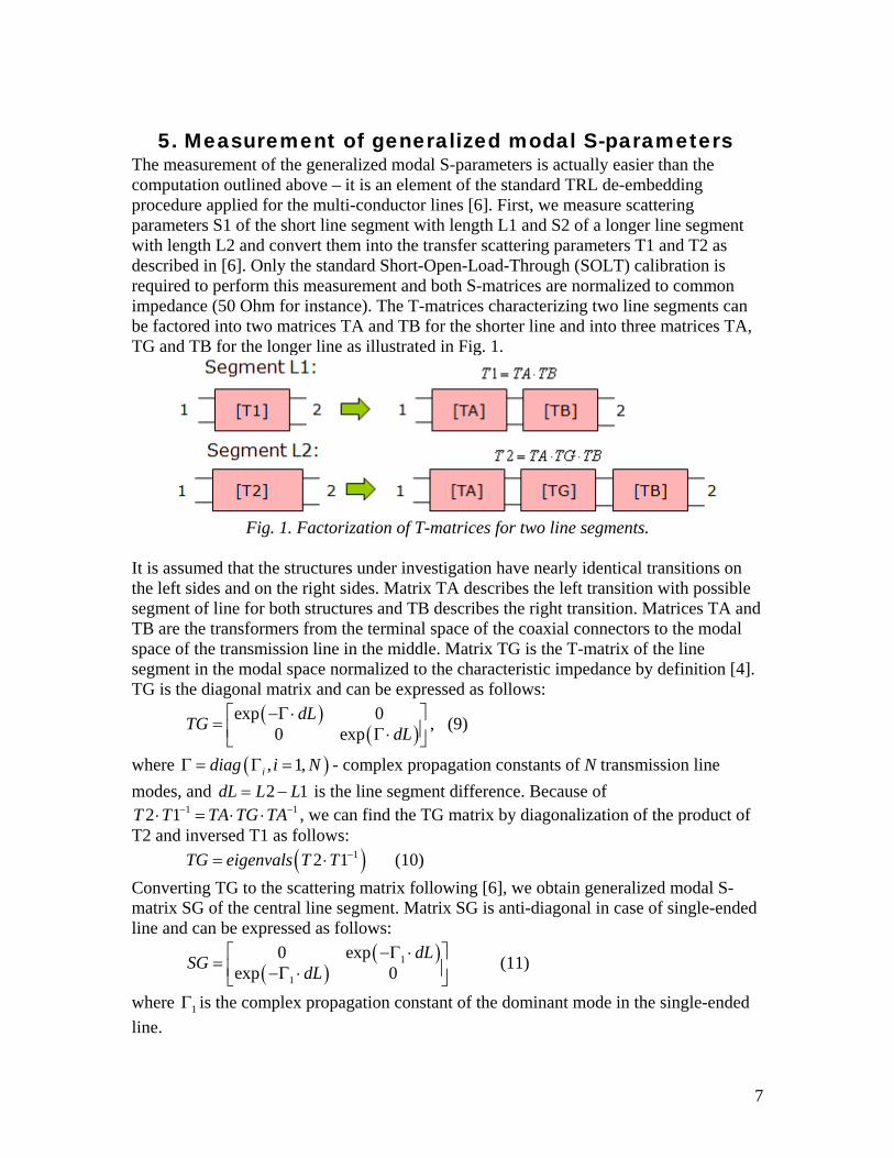
The measurement of the generalized modal S-parameters is actually easier than the computation outlined above – it is an element of the standard TRL de-embedding procedure applied for the multi-conductor lines [6]. First, we measure scattering parameters S1 of the short line segment with length L1 and S2 of a longer line segment with length L2 and convert them into the transfer scattering parameters T1 and T2 as described in [6]. Only the standard Short-Open-Load-Through (SOLT) calibration is required to perform this measurement and both S-matrices are normalized to common impedance (50 Ohm for instance). The T-matrices characterizing two line segments can be factored into two matrices TA and TB for the shorter line and into three matrices TA, TG and TB for the longer line as illustrated in Fig. 1.
Fig. 1. Factorization of T-matrices for two line segments.
It is assumed that the structures under investigation have nearly identical transitions on the left sides and on the right sides. Matrix TA describes the left transition with possible segment of line for both structures and TB describes the right transition. Matrices TA and TB are the transformers from the terminal space of the coaxial connectors to the modal space of the transmission line in the middle. Matrix TG is the T-matrix of the line segment in the modal space normalized to the characteristic impedance by definition [4]. TG is the diagonal matrix and can be expressed as follows:
( )(
exp 00 exp
dLTG dL−Γ ⋅⎡ ⎤= ⎢ ⎥Γ ⋅⎣ ⎦)
)
1−
)⋅
, (9)
where - complex propagation constants of N transmission line modes, and is the line segment difference. Because of
, we can find the TG matrix by diagonalization of the product of T2 and inversed T1 as follows:
( , 1,idiag i NΓ = Γ =2 1dL L L= −
1 TA TG TA−⋅ = ⋅ ⋅2 1T T
( 12 1TG eigenvals T T −= (10) Converting TG to the scattering matrix following [6], we obtain generalized modal S-matrix SG of the central line segment. Matrix SG is anti-diagonal in case of single-ended line and can be expressed as follows:
( )( )
1
1
0 expexp 0
dLSG dL−Γ ⋅⎡ ⎤= ⎢ ⎥−Γ ⋅⎣ ⎦
(11)
where is the complex propagation constant of the dominant mode in the single-ended line.
1Γ
7
Matrix SG is block-diagonal in case of two-conductor or differential lines and can be expressed as follows:
( )(
( )( )
1
2
1
2
0 0 exp 00 0 0 exp
exp 0 0 00 exp 0 0
dLdLSG dL
dL
−Γ ⋅⎡ ⎤⎢ ⎥−Γ ⋅= ⎢ ⎥−Γ ⋅⎢ ⎥
−Γ ⋅⎢ ⎥⎣ ⎦
1Γ 2Γ
) (12)
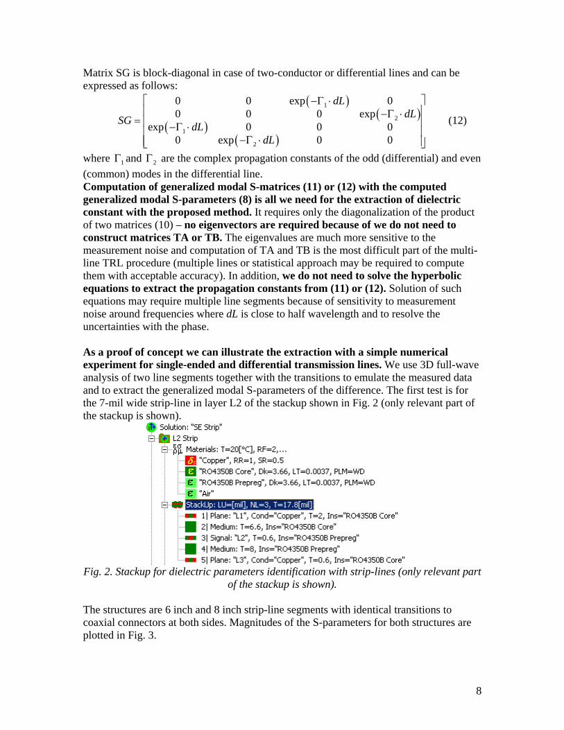
where and are the complex propagation constants of the odd (differential) and even (common) modes in the differential line. Computation of generalized modal S-matrices (11) or (12) with the computed generalized modal S-parameters (8) is all we need for the extraction of dielectric constant with the proposed method. It requires only the diagonalization of the product of two matrices (10) – no eigenvectors are required because of we do not need to construct matrices TA or TB. The eigenvalues are much more sensitive to the measurement noise and computation of TA and TB is the most difficult part of the multi-line TRL procedure (multiple lines or statistical approach may be required to compute them with acceptable accuracy). In addition, we do not need to solve the hyperbolic equations to extract the propagation constants from (11) or (12). Solution of such equations may require multiple line segments because of sensitivity to measurement noise around frequencies where dL is close to half wavelength and to resolve the uncertainties with the phase. As a proof of concept we can illustrate the extraction with a simple numerical experiment for single-ended and differential transmission lines. We use 3D full-wave analysis of two line segments together with the transitions to emulate the measured data and to extract the generalized modal S-parameters of the difference. The first test is for the 7-mil wide strip-line in layer L2 of the stackup shown in Fig. 2 (only relevant part of the stackup is shown).
Fig. 2. Stackup for dielectric parameters identification with strip-lines (only relevant part
of the stackup is shown). The structures are 6 inch and 8 inch strip-line segments with identical transitions to coaxial connectors at both sides. Magnitudes of the S-parameters for both structures are plotted in Fig. 3.
8
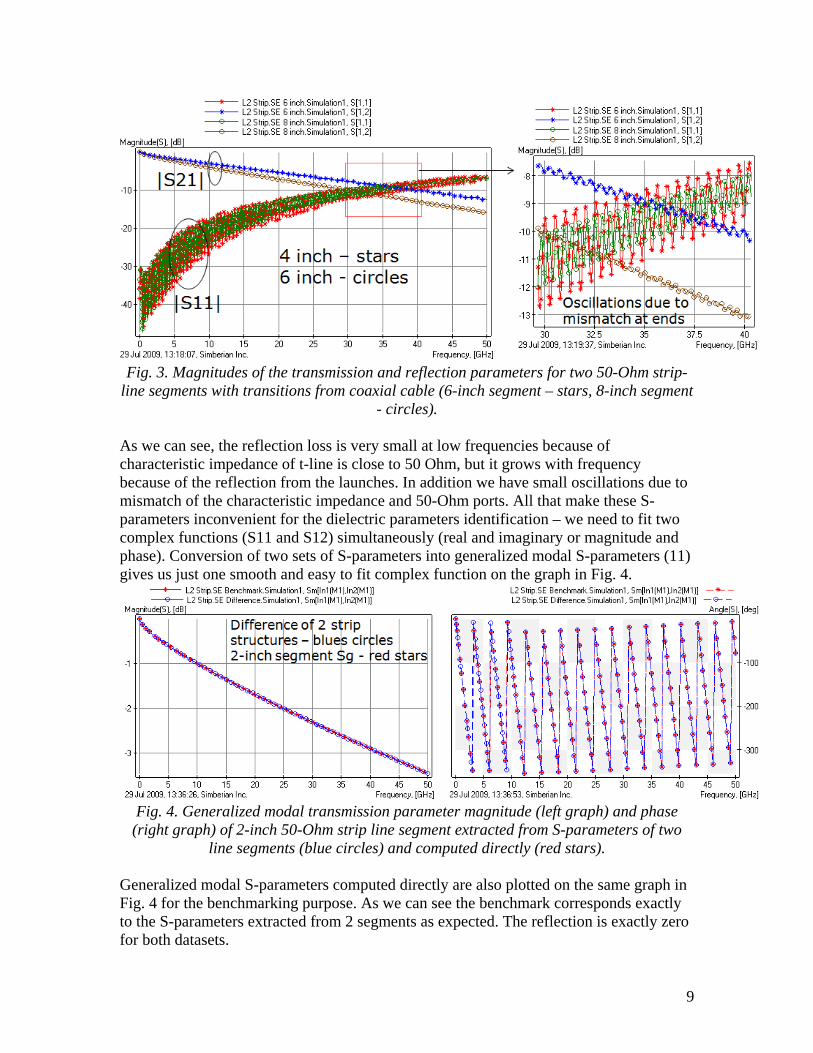
Fig. 3. Magnitudes of the transmission and reflection parameters for two 50-Ohm strip-
line segments with transitions from coaxial cable (6-inch segment – stars, 8-inch segment - circles).
As we can see, the reflection loss is very small at low frequencies because of characteristic impedance of t-line is close to 50 Ohm, but it grows with frequency because of the reflection from the launches. In addition we have small oscillations due to mismatch of the characteristic impedance and 50-Ohm ports. All that make these S-parameters inconvenient for the dielectric parameters identification – we need to fit two complex functions (S11 and S12) simultaneously (real and imaginary or magnitude and phase). Conversion of two sets of S-parameters into generalized modal S-parameters (11) gives us just one smooth and easy to fit complex function on the graph in Fig. 4.
Fig. 4. Generalized modal transmission parameter magnitude (left graph) and phase
(right graph) of 2-inch 50-Ohm strip line segment extracted from S-parameters of two line segments (blue circles) and computed directly (red stars).
Generalized modal S-parameters computed directly are also plotted on the same graph in Fig. 4 for the benchmarking purpose. As we can see the benchmark corresponds exactly to the S-parameters extracted from 2 segments as expected. The reflection is exactly zero for both datasets.
9
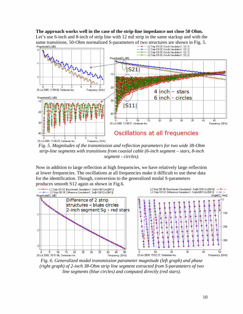
The approach works well in the case of the strip-line impedance not close 50 Ohm. Let’s use 6-inch and 8-inch of strip line with 12 mil strip in the same stackup and with the same transitions. 50-Ohm normalized S-parameters of two structures are shown in Fig. 5.
Fig. 5. Magnitudes of the transmission and reflection parameters for two wide 38-Ohm strip-line segments with transitions from coaxial cable (6-inch segment – stars, 8-inch
segment - circles). Now in addition to large reflection at high frequencies, we have relatively large reflection at lower frequencies. The oscillations at all frequencies make it difficult to use these data for the identification. Though, conversion to the generalized modal S-parameters produces smooth S12 again as shown in Fig.6.
Fig. 6. Generalized modal transmission parameter magnitude (left graph) and phase
(right graph) of 2-inch 38-Ohm strip line segment extracted from S-parameters of two line segments (blue circles) and computed directly (red stars).
10
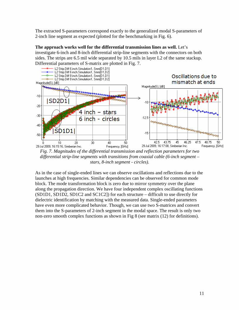
The extracted S-parameters correspond exactly to the generalized modal S-parameters of 2-inch line segment as expected (plotted for the benchmarking in Fig. 6). The approach works well for the differential transmission lines as well. Let’s investigate 6-inch and 8-inch differential strip-line segments with the connectors on both sides. The strips are 6.5 mil wide separated by 10.5 mils in layer L2 of the same stackup. Differential parameters of S-matrix are plotted in Fig. 7.
Fig. 7. Magnitudes of the differential transmission and reflection parameters for two differential strip-line segments with transitions from coaxial cable (6-inch segment –
stars, 8-inch segment - circles). As in the case of single-ended lines we can observe oscillations and reflections due to the launches at high frequencies. Similar dependencies can be observed for common mode block. The mode transformation block is zero due to mirror symmetry over the plane along the propagation direction. We have four independent complex oscillating functions (SD1D1, SD1D2, SD1C2 and SC1C2]) for each structure – difficult to use directly for dielectric identification by matching with the measured data. Single-ended parameters have even more complicated behavior. Though, we can use two S-matrices and convert them into the S-parameters of 2-inch segment in the modal space. The result is only two non-zero smooth complex functions as shown in Fig 8 (see matrix (12) for definitions).
11
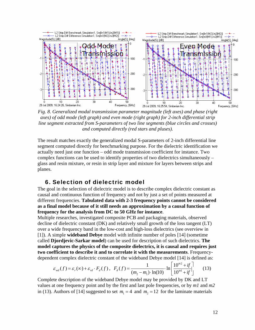
Fig. 8. Generalized modal transmission parameter magnitude (left axes) and phase (right axes) of odd mode (left graph) and even mode (right graph) for 2-inch differential strip
line segment extracted from S-parameters of two line segments (blue circles and crosses) and computed directly (red stars and pluses).
The result matches exactly the generalized modal S-parameters of 2-inch differential line segment computed directly for benchmarking purpose. For the dielectric identification we actually need just one function – odd mode transmission coefficient for instance. Two complex functions can be used to identify properties of two dielectrics simultaneously – glass and resin mixture, or resin in strip layer and mixture for layers between strips and planes.
6. Selection of dielectric model The goal in the selection of dielectric model is to describe complex dielectric constant as causal and continuous function of frequency and not by just a set of points measured at different frequencies. Tabulated data with 2-3 frequency points cannot be considered as a final model because of it still needs an approximation by a causal function of frequency for the analysis from DC to 50 GHz for instance. Multiple researches, investigated composite PCB and packaging materials, observed decline of dielectric constant (DK) and relatively small growth of the loss tangent (LT) over a wide frequency band in the low-cost and high-loss dielectrics (see overview in [1]). A simple wideband Debye model with infinite number of poles [14] (sometime called Djordjevic-Sarkar model) can be used for description of such dielectrics. The model captures the physics of the composite dielectrics, it is causal and requires just two coefficient to describe it and to correlate it with the measurements. Frequency-dependent complex dielectric constant of the wideband Debye model [14] is defined as:
( ) ( ) ( )wd r rd df F fε ε ε= ∞ + ⋅ , 2
12 1
1 10( ) ln( ) ln(10) 10
m
d m
ifF fm m if
⎡ ⎤+= ⋅ ⎢ ⎥− ⋅ +⎣ ⎦
(13)
Complete description of the wideband Debye model may be provided by DK and LT values at one frequency point and by the first and last pole frequencies, or by m1 and m2 in (13). Authors of [14] suggested to set 1 4m = and 2 12m = for the laminate materials
12
and it seems like it does not need any adjustments in practical applications from 10 KHz to 1 THz. The wideband Debye model is the simplest broad-band model for composite dielectrics and it would be great if it would be useful for all dielectric types. Unfortunately, there is evidence that it is not suitable for the low-loss dielectrics with loss tangent below 0.01. The loss tangent for some high-performance dielectrics may grow from 0.001 to 0.01 from 1 MHz to 50 GHz and this growth cannot be captured by the wideband Debye model (13). Such growth rate does not correspond to the increase of the conductor loss due to the roughness as was pointed our earlier. The only possible explanation for this growth is smaller content of the epoxy or resin in the high-performance dielectrics. The mixture of molecules in the epoxy may produce multiple Debye poles and be approximated by the continuous poles of equation (13). Higher content of glass (or glass type dielectric) causes the growth of the loss tangent similar to the one-pole Debye model that is the best for the description of pure glass. In reality the mixture may be best described by a mixture models that combines models of the resin and glass. It is easy to construct such dielectric mixture models following the analysis provided in [15]. Though, such models may be difficult to construct without extensive knowledge about the dielectric mixture components. A good alternative to the mixture model may be multi-pole Debye model with finite number of poles. Such model can be used to fit an effective DK and LT of a dielectric mixture. Multi-pole Debye model is a simple superposition of multiple one-pole Debye models [14]. It assumes that a material has multiple relaxation or polarization frequencies rnf (real poles). Formula for the relative dielectric constant of such material can be expressed as follows:
( )1
( )1
Nn
n
rn
f fif
εε ε=
Δ= ∞ +
+∑ (14)
Multi-pole Debye model with N real poles can be built with N measurements of the dielectric constant and loss tangent by fitting the measurement data with real poles at the measurement frequencies. The final model can be described by a set of the poles rnf and corresponding them residues nεΔ , and the value at infinite frequency . Multi-pole Debye model is more flexible, but at least 4-5 poles have to be used for the interconnects analysis (sometimes much more). It makes it more difficult to correlate results of transmission line segment or resonator analysis to experimental data – some numerical optimization procedure has to be used to fit the computed and measured S-parameters and smooth dependency of S-parameters is a big advantage for such optimization fit.
( )ε ∞
In this project, we use the wideband Debye model for the identification of dielectric properties of low-cost dielectrics and multi-pole Debye models for the low-loss or high-frequency dielectrics.
7. Identification of dielectric parameters Before identification of the dielectric properties, it is important to verify all dimensions of the structures on the board and to define the surface roughness of the conductors. In particular, cross-sections of the transmission lines and length difference between two line pairs have to be accurately measured before the identification. The roughness can be
13
physically measured and characterized by two parameters – RMS peak to valley distance and roughness factor. The dimensions of t-line cross-section with the impedance-controlled process may vary a little from sample to sample. Thus, just a few samples may be cross-sectioned and measured with a micrometer. With the Rdc of just strip and the known dimensions, the resistivity of the conductor can be computed. Conductor resistivity and RMS measurements of roughness and roughness factor make it possible to separate all metal losses with high confidence – it is impossible to identify the dielectric properties without such separation in the model. Note, that 2-3 um roughness gives large error in loss tangent (up to 50% or more in cases of low loss dielectrics) if not accounted for properly. The only unknown in the identification process must be the dielectric parameters. The weave effect may also have the impact on the results [16]. Considering that, the two segments of t-line have to be positioned at the distance multiple of the distance between the glass fiber (to have two lines in the pair over or off the fiber simultaneously). Another two t-line segments can be shifted by half of distance between the fibers to identify the range of the dielectric constant. Overall, the dielectric identification procedure is as follows:
1) Measure S-parameters for two line segments S1 and S2 - only SOLT calibration to the probe tips or to the coaxial connector is required
2) Estimate quality of the S-parameters – reciprocity, passivity, causality, symmetry. Either enforce the quality in case of small violations or re-measure
3) Transform S1 and S2 to the T-matrices T1 and T2, diagonalize the product of T1 and inversed T2 and extract generalized modal S-parameters of the line difference
4) Select dielectric model and guess values of the model parameters 5) Simulate segment of line with the length equal to difference and extract generalize
modal S-parameters of the segment (only modal propagation constants are required to do that as follows from the definitions (11) and (12))
6) Adjust dielectric model parameters and re-simulate the line segment to match phase and magnitude of the measured and simulated modal transmission coefficients (optionally use numerical optimization of the dielectric model)
The only tricky part of the procedure is the reliable model that allows extraction of the generalized modal S-parameters with all important dispersion and loss effects included into the complex propagation constant. Frequency-domain solver such as Simbeor [17] may be used to do it. The rest of the procedure can be easily implemented in Matlab or Mathcad and is also available as a standard feature in Simbeor 2008.01 software.
8. Practical examples To illustrate the simplified dielectric properties identification procedure, we will use PLRD-1 benchmark board [1] shown in Fig. 9. The board has multiple micro-strip transmission line segments and two strip line segments with transitions to coaxial connectors on low-cost high-loss FR4 dielectric. We can use 1.75 inch and 3.5 inch micro-strip through standards marked as L1 and L2 in the bottom part in Fig. 9. Stack-up of the board with preliminary defined dielectric parameters is shown in Fig. 10. Micro-strip trace width is 17 mil for all through and line standards.
14
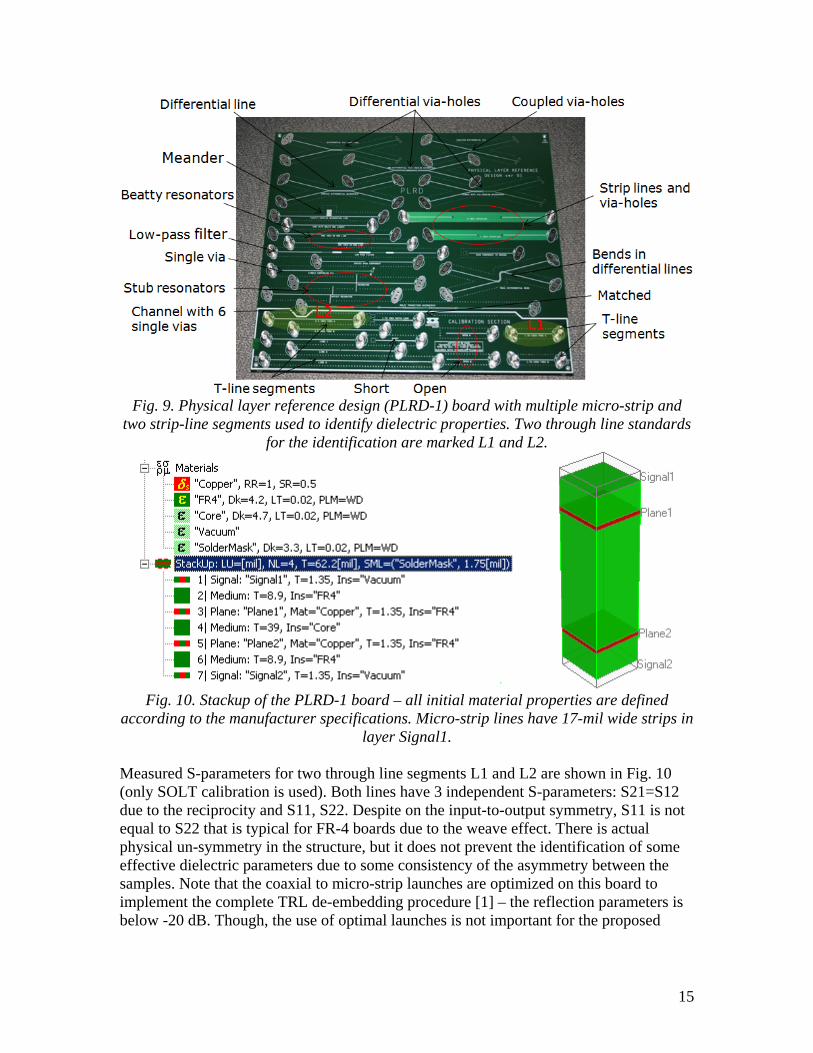
Fig. 9. Physical layer reference design (PLRD-1) board with multiple micro-strip and
two strip-line segments used to identify dielectric properties. Two through line standards for the identification are marked L1 and L2.
Fig. 10. Stackup of the PLRD-1 board – all initial material properties are defined
according to the manufacturer specifications. Micro-strip lines have 17-mil wide strips in layer Signal1.
Measured S-parameters for two through line segments L1 and L2 are shown in Fig. 10 (only SOLT calibration is used). Both lines have 3 independent S-parameters: S21=S12 due to the reciprocity and S11, S22. Despite on the input-to-output symmetry, S11 is not equal to S22 that is typical for FR-4 boards due to the weave effect. There is actual physical un-symmetry in the structure, but it does not prevent the identification of some effective dielectric parameters due to some consistency of the asymmetry between the samples. Note that the coaxial to micro-strip launches are optimized on this board to implement the complete TRL de-embedding procedure [1] – the reflection parameters is below -20 dB. Though, the use of optimal launches is not important for the proposed
15
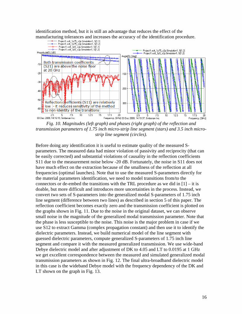
identification method, but it is still an advantage that reduces the effect of the manufacturing tolerances and increases the accuracy of the identification procedure.
Fig. 10. Magnitudes (left graph) and phases (right graph) of the reflection and
transmission parameters of 1.75 inch micro-strip line segment (stars) and 3.5 inch micro-strip line segment (circles).
Before doing any identification it is useful to estimate quality of the measured S-parameters. The measured data had minor violation of passivity and reciprocity (that can be easily corrected) and substantial violations of causality in the reflection coefficients S11 due to the measurement noise below -20 dB. Fortunately, the noise in S11 does not have much effect on the extraction because of the smallness of the reflection at all frequencies (optimal launches). Note that to use the measured S-parameters directly for the material parameters identification, we need to model transitions from/to the connectors or de-embed the transitions with the TRL procedure as we did in [1] – it is doable, but more difficult and introduces more uncertainties in the process. Instead, we convert two sets of S-parameters into the generalized modal S-parameters of 1.75 inch line segment (difference between two lines) as described in section 5 of this paper. The reflection coefficient becomes exactly zero and the transmission coefficient is plotted on the graphs shown in Fig. 11. Due to the noise in the original dataset, we can observe small noise in the magnitude of the generalized modal transmission parameter. Note that the phase is less susceptible to the noise. This noise is the major problem in case if we use S12 to extract Gamma (complex propagation constant) and then use it to identify the dielectric parameters. Instead, we build numerical model of the line segment with guessed dielectric parameters, compute generalized S-parameters of 1.75 inch line segment and compare it with the measured generalized transmission. We use wide-band Debye dielectric model and after adjustment of DK to 4.05 and LT to 0.0195 at 1 GHz we get excellent correspondence between the measured and simulated generalized modal transmission parameters as shown in Fig. 12. The final ultra-broadband dielectric model in this case is the wideband Debye model with the frequency dependency of the DK and LT shown on the graph in Fig. 13.
16
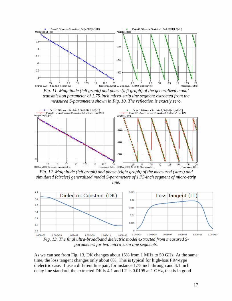
Fig. 11. Magnitude (left graph) and phase (left graph) of the generalized modal transmission parameter of 1.75-inch micro-strip line segment extracted from the
measured S-parameters shown in Fig. 10. The reflection is exactly zero.
Fig. 12. Magnitude (left graph) and phase (right graph) of the measured (stars) and
simulated (circles) generalized modal S-parameters of 1.75-inch segment of micro-strip line.
Fig. 13. The final ultra-broadband dielectric model extracted from measured S-
parameters for two micro-strip line segments. As we can see from Fig. 13, DK changes about 15% from 1 MHz to 50 GHz. At the same time, the loss tangent changes only about 8%. This is typical for high-loss FR4-type dielectric case. If use a different line pair, for instance 1.75 inch through and 4.1 inch delay line standard, the extracted DK is 4.1 and LT is 0.0195 at 1 GHz, that is in good
17
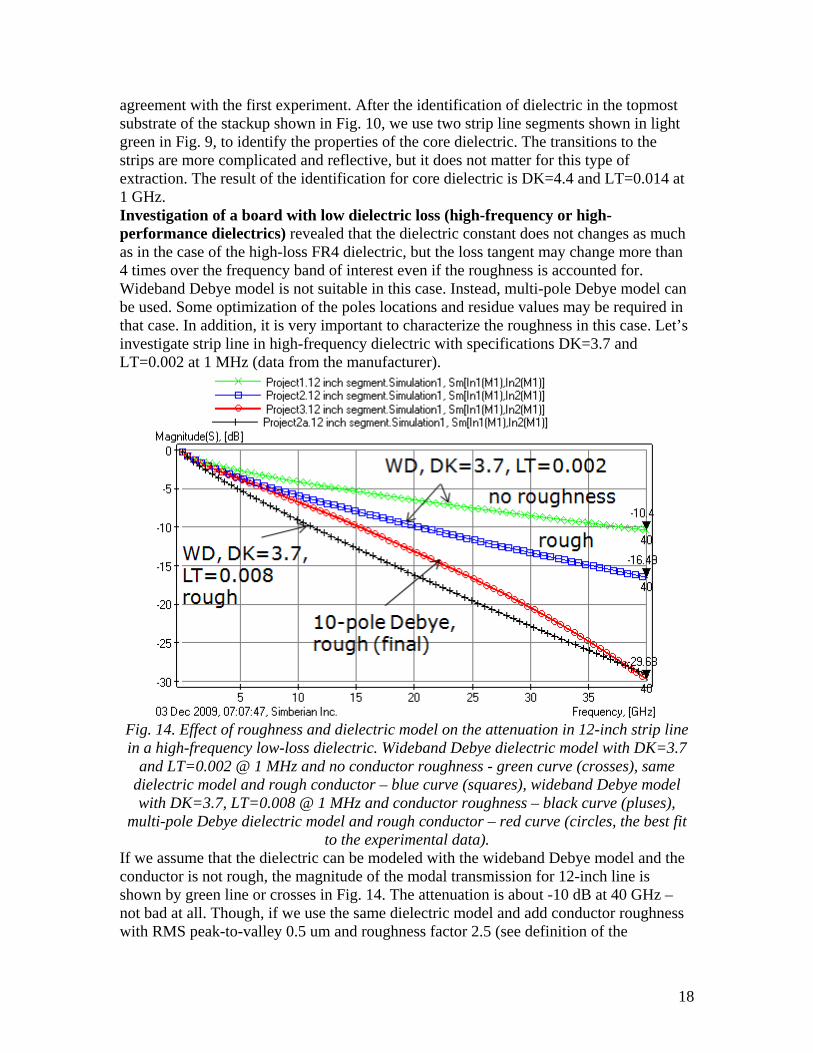
agreement with the first experiment. After the identification of dielectric in the topmost substrate of the stackup shown in Fig. 10, we use two strip line segments shown in light green in Fig. 9, to identify the properties of the core dielectric. The transitions to the strips are more complicated and reflective, but it does not matter for this type of extraction. The result of the identification for core dielectric is DK=4.4 and LT=0.014 at 1 GHz. Investigation of a board with low dielectric loss (high-frequency or high-performance dielectrics) revealed that the dielectric constant does not changes as much as in the case of the high-loss FR4 dielectric, but the loss tangent may change more than 4 times over the frequency band of interest even if the roughness is accounted for. Wideband Debye model is not suitable in this case. Instead, multi-pole Debye model can be used. Some optimization of the poles locations and residue values may be required in that case. In addition, it is very important to characterize the roughness in this case. Let’s investigate strip line in high-frequency dielectric with specifications DK=3.7 and LT=0.002 at 1 MHz (data from the manufacturer).
Fig. 14. Effect of roughness and dielectric model on the attenuation in 12-inch strip line in a high-frequency low-loss dielectric. Wideband Debye dielectric model with DK=3.7
and LT=0.002 @ 1 MHz and no conductor roughness - green curve (crosses), same dielectric model and rough conductor – blue curve (squares), wideband Debye model with DK=3.7, LT=0.008 @ 1 MHz and conductor roughness – black curve (pluses),
multi-pole Debye dielectric model and rough conductor – red curve (circles, the best fit to the experimental data).
If we assume that the dielectric can be modeled with the wideband Debye model and the conductor is not rough, the magnitude of the modal transmission for 12-inch line is shown by green line or crosses in Fig. 14. The attenuation is about -10 dB at 40 GHz – not bad at all. Though, if we use the same dielectric model and add conductor roughness with RMS peak-to-valley 0.5 um and roughness factor 2.5 (see definition of the
18
roughness parameters in [1]), the attenuation in 12-inch strip segment increases about 25% at 3 GHz to 65% at 40 GHz (-16.5 dB) as shown by blue curve with squares in Fig. 14. If we simply increase the loss tangent in the wideband Debye model from 0.002 to 0.008 and keep conductor rough, the attenuation at 40 GHz will be close to the experimental, but the attenuation at low and medium frequencies will be over-estimated as shown by black curve with pluses in Fig. 14. In addition the phases of the transmission parameters will not be matched with such adjustment. The final dielectric identification result with the rough conductors was 10-pole dielectric model that produced about -30 dB attenuation at 40 GHz as shown by red curve with circles in Fig. 14. The model with 10-pole dielectric matched very well to the actual measured attenuation (not shown on the graph due to the confidentiality of the research materials).
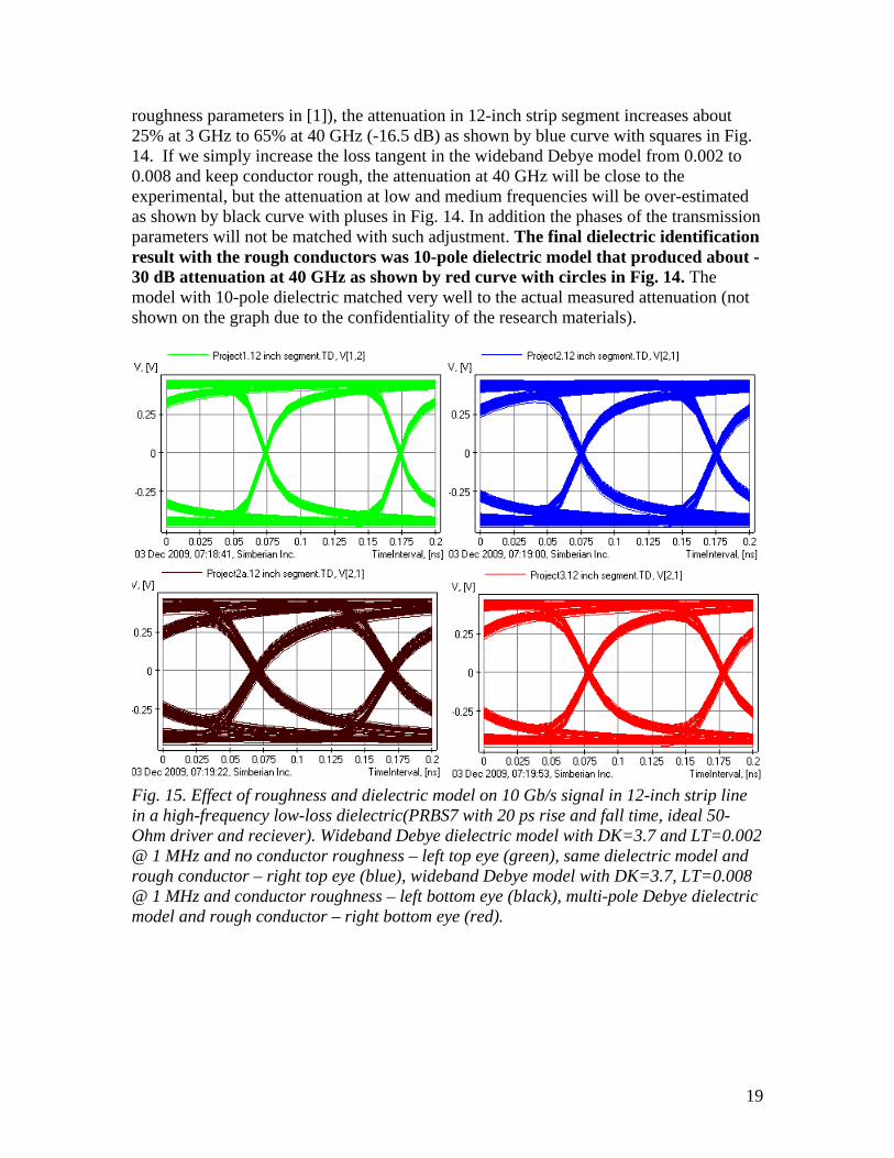
Fig. 15. Effect of roughness and dielectric model on 10 Gb/s signal in 12-inch strip line in a high-frequency low-loss dielectric(PRBS7 with 20 ps rise and fall time, ideal 50-Ohm driver and reciever). Wideband Debye dielectric model with DK=3.7 and LT=0.002 @ 1 MHz and no conductor roughness – left top eye (green), same dielectric model and rough conductor – right top eye (blue), wideband Debye model with DK=3.7, LT=0.008 @ 1 MHz and conductor roughness – left bottom eye (black), multi-pole Debye dielectric model and rough conductor – right bottom eye (red).
19
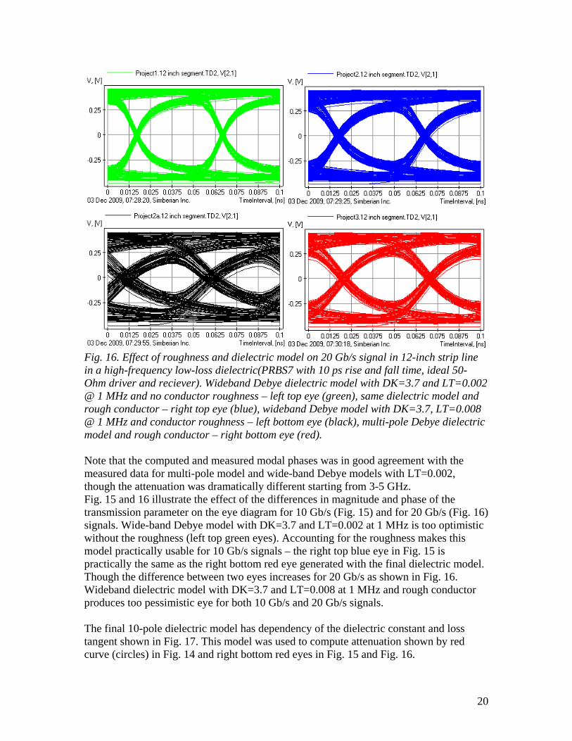
Fig. 16. Effect of roughness and dielectric model on 20 Gb/s signal in 12-inch strip line in a high-frequency low-loss dielectric(PRBS7 with 10 ps rise and fall time, ideal 50-Ohm driver and reciever). Wideband Debye dielectric model with DK=3.7 and LT=0.002 @ 1 MHz and no conductor roughness – left top eye (green), same dielectric model and rough conductor – right top eye (blue), wideband Debye model with DK=3.7, LT=0.008 @ 1 MHz and conductor roughness – left bottom eye (black), multi-pole Debye dielectric model and rough conductor – right bottom eye (red). Note that the computed and measured modal phases was in good agreement with the measured data for multi-pole model and wide-band Debye models with LT=0.002, though the attenuation was dramatically different starting from 3-5 GHz. Fig. 15 and 16 illustrate the effect of the differences in magnitude and phase of the transmission parameter on the eye diagram for 10 Gb/s (Fig. 15) and for 20 Gb/s (Fig. 16) signals. Wide-band Debye model with DK=3.7 and LT=0.002 at 1 MHz is too optimistic without the roughness (left top green eyes). Accounting for the roughness makes this model practically usable for 10 Gb/s signals – the right top blue eye in Fig. 15 is practically the same as the right bottom red eye generated with the final dielectric model. Though the difference between two eyes increases for 20 Gb/s as shown in Fig. 16. Wideband dielectric model with DK=3.7 and LT=0.008 at 1 MHz and rough conductor produces too pessimistic eye for both 10 Gb/s and 20 Gb/s signals. The final 10-pole dielectric model has dependency of the dielectric constant and loss tangent shown in Fig. 17. This model was used to compute attenuation shown by red curve (circles) in Fig. 14 and right bottom red eyes in Fig. 15 and Fig. 16.
20
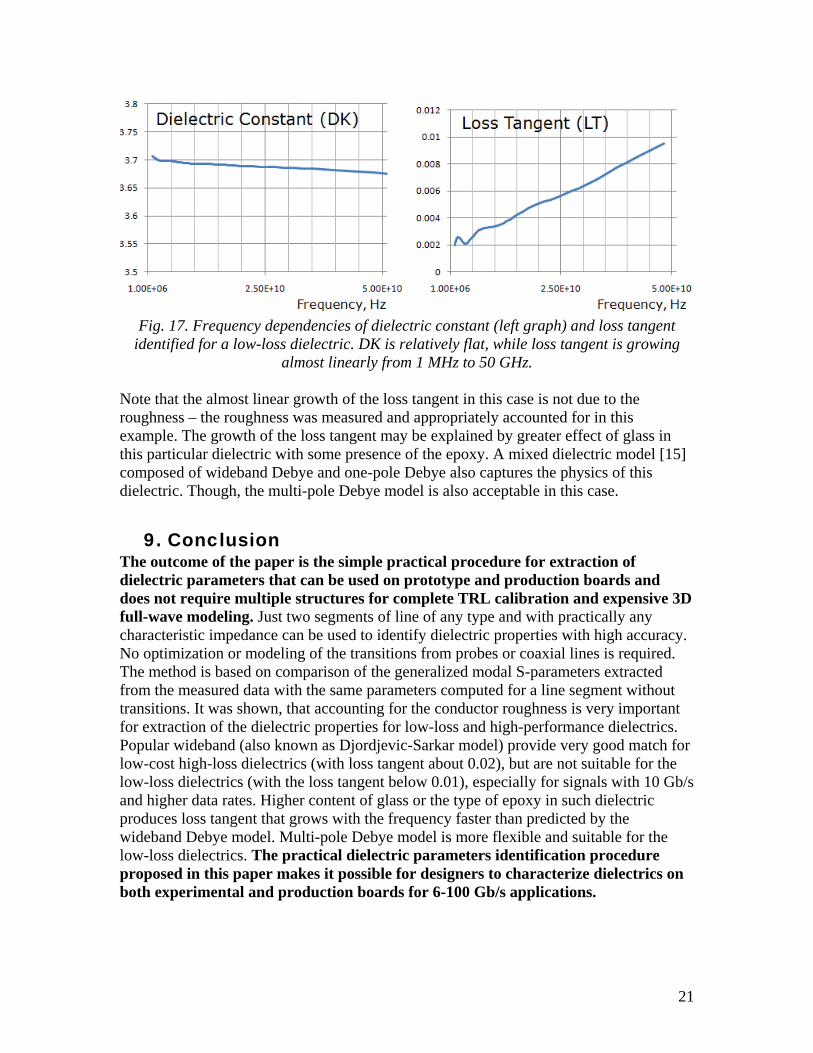
Fig. 17. Frequency dependencies of dielectric constant (left graph) and loss tangent
identified for a low-loss dielectric. DK is relatively flat, while loss tangent is growing almost linearly from 1 MHz to 50 GHz.
Note that the almost linear growth of the loss tangent in this case is not due to the roughness – the roughness was measured and appropriately accounted for in this example. The growth of the loss tangent may be explained by greater effect of glass in this particular dielectric with some presence of the epoxy. A mixed dielectric model [15] composed of wideband Debye and one-pole Debye also captures the physics of this dielectric. Though, the multi-pole Debye model is also acceptable in this case.
9. Conclusion The outcome of the paper is the simple practical procedure for extraction of dielectric parameters that can be used on prototype and production boards and does not require multiple structures for complete TRL calibration and expensive 3D full-wave modeling. Just two segments of line of any type and with practically any characteristic impedance can be used to identify dielectric properties with high accuracy. No optimization or modeling of the transitions from probes or coaxial lines is required. The method is based on comparison of the generalized modal S-parameters extracted from the measured data with the same parameters computed for a line segment without transitions. It was shown, that accounting for the conductor roughness is very important for extraction of the dielectric properties for low-loss and high-performance dielectrics. Popular wideband (also known as Djordjevic-Sarkar model) provide very good match for low-cost high-loss dielectrics (with loss tangent about 0.02), but are not suitable for the low-loss dielectrics (with the loss tangent below 0.01), especially for signals with 10 Gb/s and higher data rates. Higher content of glass or the type of epoxy in such dielectric produces loss tangent that grows with the frequency faster than predicted by the wideband Debye model. Multi-pole Debye model is more flexible and suitable for the low-loss dielectrics. The practical dielectric parameters identification procedure proposed in this paper makes it possible for designers to characterize dielectrics on both experimental and production boards for 6-100 Gb/s applications.
21
10. Appendix A: Alternative approaches for
identification of PCB dielectric properties As an alternative to the suggested technique, de-embedded transmission line segments or resonators can be used to identify the dielectric parameters by comparison of the S-parameters – see [1] and reference there. In reality such procedure requires a great deal of experience in the frequency domain measurements and de-embedding to obtain high-quality models. In addition, it is very difficult to implement the complete Trough-Reflect-Line (TRL) de-embedding procedure on production or prototype PC boards just for the material parameters extraction purpose. Another possibility is to reduce the number of line segments or resonators for the dielectric parameters extraction to just one. It seems like a simplification at first, but it increases the complexity of the extraction procedure. The transitions from the probes or connectors have to be reliably characterized with a 3D full-wave analysis - it may require separate validation and may be even not possible due to non-localizability of the problem. In addition, magnitude and phase have to be matched both for the reflection and transmission coefficients. Such matching may be not trivial due to the resonances from the transitions – simple optimization may fail. The identification with one line segment is possible, but requires high skills both in measurements and in 3D full-wave analysis and expensive electromagnetic software. Another alternative is the multi-line technique with the diagonalization of T-matrices that was recently used by many authors [2]-[6] to extract complex propagation constants (Gamma) for transmission lines. Though, it looks like that such technique with the T-matrix diagonalization was first proposed in late 70-s by Nikol’skiy and Lavrova in [7]. The basis of the methods with Gamma is the fact that the diagonal T-matrix in the multi-line TRL de-embedding contains only elements defined by the complex propagation constant and independent of the characteristic impedance [4]. The diagonal T-matrix of central segment (with the length equal to the difference of lines) is normalized to the characteristic impedance of the strip/micro-strip, differential or coplanar line modes. This is the result of the diagonalization of the scattering transfer matrix (T-matrix) of the central segment. The diagonal T-matrix corresponds to the block-diagonal S-matrix with only diagonal elements in blocks S12 and S21 not equal to zero and zero reflection and transformation elements (S-matrix is anti-diagonal in case of single-ended line). S-matrix of a line segment without reflection is normalized to the characteristic impedance of the line modes by definition (no actual knowledge of the impedance is required at this stage). Paper [4] uses slightly different explanation of the effect - but the idea of the reflection-less segment is the same. The fact that the diagonal T-matrix of TRL de-embedding provides generalized modal S-parameters was also noticed in [6] for multi-conductor line cases. Unfortunately, all techniques with Gamma extraction are very sensitive to the imperfections in the test structures and in addition they still require a model to compute complex dielectric constant from the complex propagation constant [2], [3]. The most difficult part of all approaches based on Gamma is the solution of the hyperbolic equations with the measurement noise and large errors when the length difference between the line segments is half of wavelength. Identification of the propagation constant over a wide frequency band requires more than two line segments and additional short and open structures as in [2].
22
In addition, even strip-line configurations do not provide an easy way to extract the propagation constant because of the dependency of Gamma on the conductor loss and dispersion, conductor roughness and high-frequency dispersion due to in-homogeneity of the dielectric layers adjacent to the strip in the PCB applications (the effect of FR-4 dielectric in-homogeneity in strip-line configurations is interpreted in [18] as the uniaxial anisotropy of the effective dielectric constant and loss tangent). The high-frequency dispersion is even more critical in cases if micro-strip structures are used for the identification (micro-strip structures may have advantage due to simpler transitions from probes or coaxial lines). Approximate formulas used to convert Gamma into dielectric constant may lead to different types of defects – such as overestimated loss tangent due to not accounting for the conductor roughness or plating. It means that simplified formula-based models or static and quasi-static solutions are practically useless above 3-5 GHz both for the dielectric parameters identification and for the compliance analysis. In this paper we use 3D full-wave electromagnetic analysis to compute generalized modal S-parameters of a line segment with all types of conductor and dielectric losses and dispersion included. The dielectric model is derived by comparison of the measured and computed generalized modal S-parameters.
11. References 1. Y. Shlepnev, A. Neves, T. Dagostino, S. McMorrow, Measurement-Assisted
Electromagnetic Extraction of Interconnect Parameters on Low-Cost FR-4 boards for 6-20 Gb/sec Applications, DesignCon2009.
2. M. Cauwe, J. De Baets, Broadband material parameter characterization for practical high-speed interconnects on printed circuit boards, IEEE Trans, v. 31, 2008, N 3, p. 649-656.
3. F. Declercq, H. Rogier, C. Hertleer , Permittivity and Loss Tangent Characterization for Garment Antennas Based on a New Matrix-Pencil Two-Line Method, IEEE Trans. on AP, vol. 56, 2008 N8, p. 2548-2554.
4. D.C. DeGroot, D.K. Walker, and R.B. Marks, Impedance Mismatch Effects On Propagation Constant Measurements - IEEE EPEP Conf. Dig., Napa, CA, Oct. 28-30, 1996, pp. 141-143.
5. R. B. Marks, “A multiline method of network analyzer calibration,” IEEE Trans. Microwave Theory Tech., vol. 39, no. 7, 1991, p. 1205–1215.
6. Seguinot et al.: Multimode TRL – A new concept in microwave measurements, IEEE Trans. on MTT, vol. 46, 1998, N 5, p. 536-542.
7. V.V. Nikol’skiy, T.I. Lavrova, Solution of characteristic mode problems by the method of minimum autonomous blocks, Radio Eng. & Electronic Physics, 1979, v. 24, N 8, p.26-33.
8. C. R. Paul, Decoupling the multiconductor transmission line equations, IEEE Trans. on MTT, v. 44, No. 8, 1996, p. 1429-1440.
9. D. F. Williams, L. A. Hayden, R. B. Marks, A complete multimode equivalent-circuit theory for electrical design, Journal of Research of the National Institute of Standards and Technology, v. 102, No. 4, 1997, p. 405-423.
10. D. F. Williams, J. E. Rogers, C. L. Holloway, Multiconductor transmission line characterization: Representations, approximations, and accuracy, IEEE Trans. on MTT, v. 47, No. 4, 1999, p. 403-409.
23
24
11. Y.O. Shlepnev, Extension of the Method of Lines for planar 3D structures - in Proceedings of the 15th Annual Review of Progress in Applied Computational Electromagnetics (ACES'99), Monterey, CA, 1999, p.116-121.
12. Y.O. Shlepnev, Trefftz finite elements for electromagnetics, IEEE Trans. Microwave Theory Tech., vol. MTT-50, pp. 1328-1339, May, 2002.
13. Y. O. Shlepnev, B.V. Sestroretzkiy, V.Y. Kustov, A new approach to modeling arbitrary transmission lines. - Journal of Communications Technology and Electronics, v. 42, 1997, N 1, p. 13-16.
14. Djordjevic, R.M. Biljic, V.D. Likar-Smiljanic, T.K.Sarkar, Wideband frequency domain characterization of FR-4 and time-domain causality, IEEE Trans. on EMC, vol. 43, N4, 2001, p. 662-667.
15. K.K. Kärkkäinen, A.H. Sihvola, and K.I. Nikoskinen, Effective Permittivity of Mixtures: Numerical Validation by the FDTD Method, IEEE Trans. on Geosciences and Remote Sensing, v. 38, No. 3, 2000, p. 1303-1308.
16. S. McMorrow, C. Head, “The Impact of PCB Laminate Weave on the Electrical Performance of Differential Signaling at Multi-gigabit Data Rates”, IEC Designcon East 2005 (available at www.teraspeed.com).
17. Simbeor 2008.01 Electromagnetic Signal Integrity Software, www.simberian.com 18. J.C. Rautio, S. Arvas, Measurement of planar substrate uniaxial anisotropy, IEEE
Trans. on MTT, vo. 57, N10, 2009, p. 2456-2463.