
Power Electronicsee.cet.ac.in/downloads/Notes/PE/PE5-Inverters.pdf · Power Electronics INVERTERS...
32
Power Electronics INVERTERS DEPT. OF ELECTRICAL ENGINEERING, COLLEGE OF ENGINEERING TRIVANDRUM 2018 Dr. Francis M. Fernandez
Transcript of Power Electronicsee.cet.ac.in/downloads/Notes/PE/PE5-Inverters.pdf · Power Electronics INVERTERS...
Power Electronics
INVERTERS
DEPT. OF ELECTRICAL ENGINEERING, COLLEGE OF ENGINEERING TRIVANDRUM
2018 Dr. Francis M. Fernandez

Inverter Classification
Classification of inverters based on wave shape
Square wave
Quasi square wave
Sine wave
Classification of inverters based on Input
Voltage source
Current source
2DEPT. OF ELECTRICAL ENGINEERING, COLLEGE OF ENGINEERING TRIVANDRUM

Half bridge inverter
DEPT. OF ELECTRICAL ENGINEERING, COLLEGE OF ENGINEERING TRIVANDRUM 3
2DCE
2DCE
Switches S1 and S2 used are gate commutated devices such as BJT, MOSFET, IGBT, GTO etc
S1 and S2 are turned on alternately to produce an ac voltage across the load
Each switch is ON for half time period (T/2) of the desired frequency

Full bridge inverter
DEPT. OF ELECTRICAL ENGINEERING, COLLEGE OF ENGINEERING TRIVANDRUM 4
S1 and S2 turned on in the first half cycle (T/2)
S3 and S4 turned on in the second half cycle (T/2)

Full bridge inverter – R load
DEPT. OF ELECTRICAL ENGINEERING, COLLEGE OF ENGINEERING TRIVANDRUM 5
Two modes of operation:Mode 1:
S1 and S2 are ONMode 2
S3 and S4 are ON

Full bridge inverter – RL load
DEPT. OF ELECTRICAL ENGINEERING, COLLEGE OF ENGINEERING TRIVANDRUM 6
Four modes of operation:
Mode 1: S1 and S2 are ON, Output +ve
Mode 2: D3, D4 conducts, Output -ve
Mode 3: S3 and S4 are ON, Output –ve
Mode 4: D1, D2 conducts, Output +ve

Full Bridge Inverter – Transistor Ratings
DEPT. OF ELECTRICAL ENGINEERING, COLLEGE OF ENGINEERING TRIVANDRUM 7
DCCE EV )0(
R
EI DC
aveT2
)(
R
EI DC
peakT )(

Harmonics
DEPT. OF ELECTRICAL ENGINEERING, COLLEGE OF ENGINEERING TRIVANDRUM 8
1,3,5,..
Fourier series for symmetrical square wave4
, sin
DC
n
Ee n t
n
Original square wave
Fundamental component
Third order harmonic
Fifth order harmonic
Seventh order harmonic

Harmonics
DEPT. OF ELECTRICAL ENGINEERING, COLLEGE OF ENGINEERING TRIVANDRUM 9
IL
VL
tnn
Ee
n
DC
sin4
,SeriesFourier,..5,3,1
1
1
2 2Fundamental output voltage,
. 0.9
DC
DC
E E
ie E E
th 1n order output voltage, n
EE
n
2 2 2( ) 1 3 5RMS value, ...rmsE E E E
1
2 12 2 2 2
13,5,..
Harmonic voltage, 0.4352h n DCn
E E E E E
(rms)
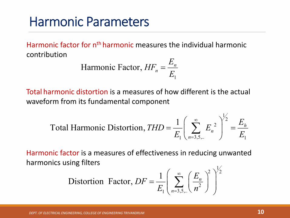
Harmonic Parameters
DEPT. OF ELECTRICAL ENGINEERING, COLLEGE OF ENGINEERING TRIVANDRUM 10
12 2
23,5,..1
1Distortion Factor,
n
n
EDF
E n
12
2
3,5,..1 1
1Total Harmonic Distortion,
h
nn
ETHD E
E E
1
Harmonic Factor, nn
EHF
E
Harmonic factor for nth harmonic measures the individual harmonic contribution
Total harmonic distortion is a measures of how different is the actual waveform from its fundamental component
Harmonic factor is a measures of effectiveness in reducing unwanted harmonics using filters

Comparison of parameters in Half Bridge and Full Bridge Inverters
DEPT. OF ELECTRICAL ENGINEERING, COLLEGE OF ENGINEERING TRIVANDRUM 11
1
2 20.9
DC DCE E E 1
2 20.45
2 DC
DC
EE E
O DCE E2
DCO
EE
BR DCE E BR DCE E
0.4352h DCE E 0.2176h DCE E
Output voltage
Fundamentaloutput voltage
Harmonicoutput voltage
Peak breaking voltage of switches
Full Bridge Half Bridge

Example
A single phase full bridge inverter is operated from 48 V battery andsupplying power to a 24 ohm load. Determine output power THD ofoutput and transistor ratings.
12DEPT. OF ELECTRICAL ENGINEERING, COLLEGE OF ENGINEERING TRIVANDRUM
2 248RMS Power, 96 W
24
EP
R
48 VCEV
( )
482A
24
DCT peak
EI
R
Solution:
1 0.9 0.9 48 43.2 VDCE E
0.4352 0.4352 48 20.89 Vh DCE E
1
20.8948.36 %
43.2hETHDE

Cross Conduction or Shoot Through Fault
DEPT. OF ELECTRICAL ENGINEERING, COLLEGE OF ENGINEERING TRIVANDRUM 13
Normally the switches in the bridgeswitch on in pairs – S1-S2 turn onfirst and after they are off, S3-S4turn on
Therefore the switches in the sameleg (say S1 and S4) may not turn onat the same time
Due to turn off delay, incomingdevice and outgoing device of thesame leg in the bridge conduct atthe same instant and short circuitsthe DC source.
This fault damages both the devices
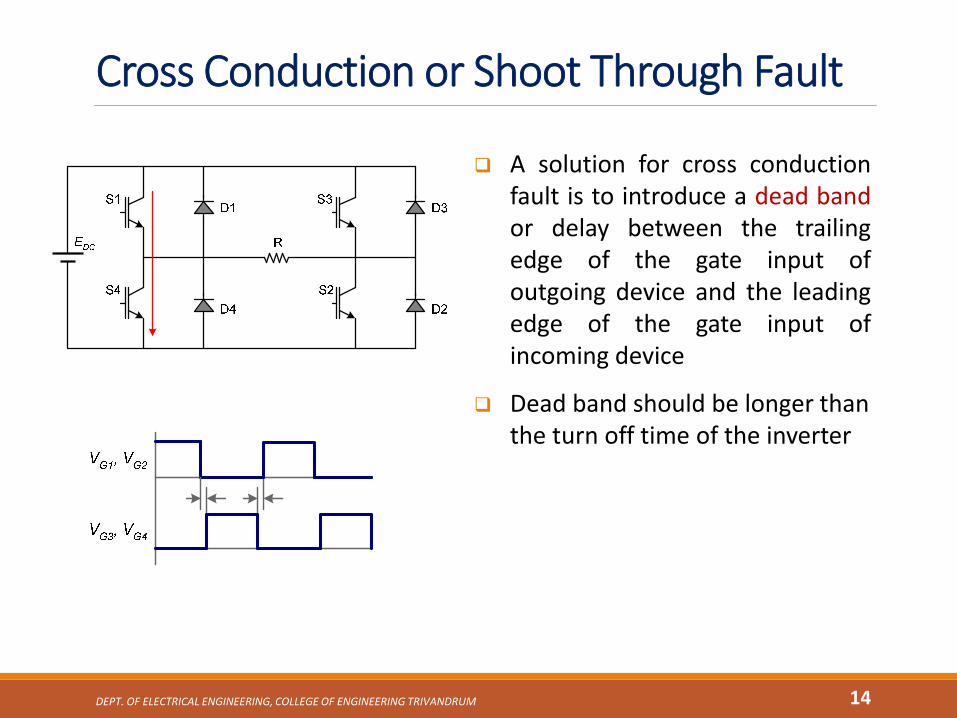
Cross Conduction or Shoot Through Fault
DEPT. OF ELECTRICAL ENGINEERING, COLLEGE OF ENGINEERING TRIVANDRUM 14
A solution for cross conductionfault is to introduce a dead bandor delay between the trailingedge of the gate input ofoutgoing device and the leadingedge of the gate input ofincoming device
Dead band should be longer than the turn off time of the inverter

3-Phase Inverter
DEPT. OF ELECTRICAL ENGINEERING, COLLEGE OF ENGINEERING TRIVANDRUM 15
A
C
B
RR
R
Load configurations
AB
C
S1 D1
S4 D4 S6
S3 D3
D6
EDC
S2
S5 D5
D2
ThreePhaseLoad

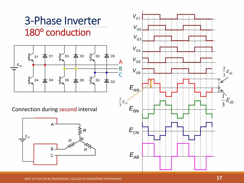
3-Phase Inverter180° conduction
DEPT. OF ELECTRICAL ENGINEERING, COLLEGE OF ENGINEERING TRIVANDRUM 16
ABC
N
Connection during first interval
S1 D1
S4 D4 S6
S3 D3
D6
EDC
S2
S5 D5
D2
DCE3
1 dcE3
1
dcE3
2
3-Phase Inverter180° conduction
DEPT. OF ELECTRICAL ENGINEERING, COLLEGE OF ENGINEERING TRIVANDRUM 17
ABC
S1 D1
S4 D4 S6
S3 D3
D6
EDC
S2
S5 D5
D2
dcE3
1
dcE3
2
N
Connection during second intervalDCE
3
2

3-Phase Inverter180° conduction
DEPT. OF ELECTRICAL ENGINEERING, COLLEGE OF ENGINEERING TRIVANDRUM 18
ABC
S1 D1
S4 D4 S6
S3 D3
D6
EDC
S2
S5 D5
D2
dcE3
1
dcE3
2
IntervalIncoming
DeviceConducting
Devices
1 S1 5,6,1
2 S1 6,1,2
3 S3 1,2,3
4 S4 2,3,4
5 S5 3,4,5
6 S6 4,5,6
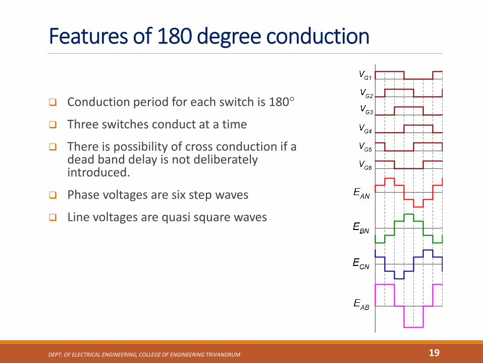
Features of 180 degree conduction
Conduction period for each switch is 180°
Three switches conduct at a time
There is possibility of cross conduction if a dead band delay is not deliberately introduced.
Phase voltages are six step waves
Line voltages are quasi square waves
19DEPT. OF ELECTRICAL ENGINEERING, COLLEGE OF ENGINEERING TRIVANDRUM
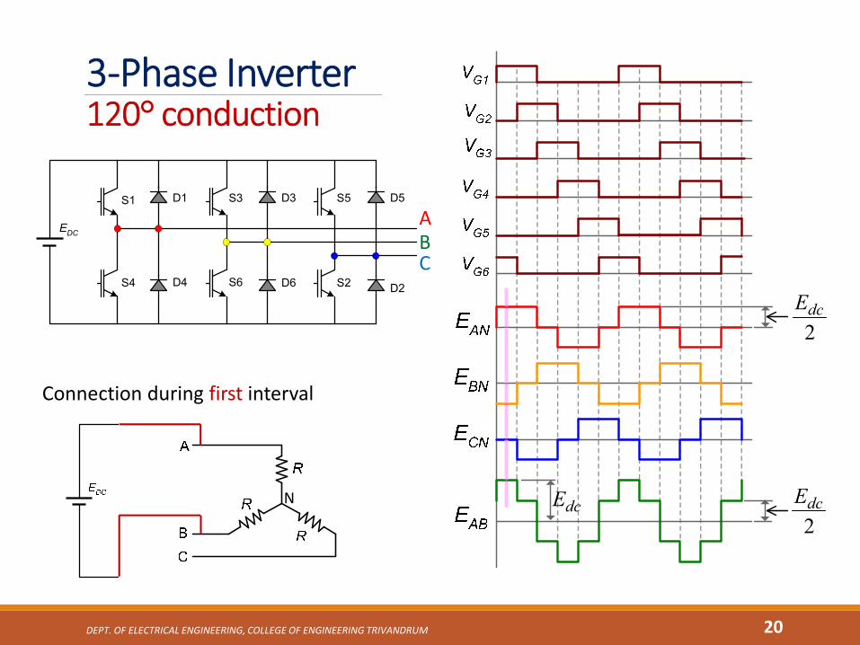
3-Phase Inverter120° conduction
DEPT. OF ELECTRICAL ENGINEERING, COLLEGE OF ENGINEERING TRIVANDRUM 20
ABC
S1 D1
S4 D4 S6
S3 D3
D6
EDC
S2
S5 D5
D2
N
Connection during first interval
2dcE
dcE
2dcE

3-Phase Inverter120° conduction
DEPT. OF ELECTRICAL ENGINEERING, COLLEGE OF ENGINEERING TRIVANDRUM 21
ABC
S1 D1
S4 D4 S6
S3 D3
D6
EDC
S2
S5 D5
D2
2dcE
dcE
2dcEN
Connection during second interval

3-Phase Inverter120° conduction
DEPT. OF ELECTRICAL ENGINEERING, COLLEGE OF ENGINEERING TRIVANDRUM 22
ABC
S1 D1
S4 D4 S6
S3 D3
D6
EDC
S2
S5 D5
D2
2dcE
dcE
2dcEN
Connection during third interval
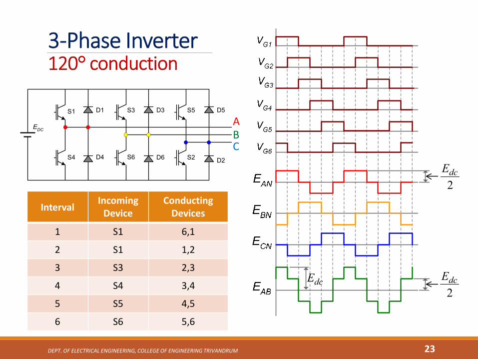
3-Phase Inverter120° conduction
DEPT. OF ELECTRICAL ENGINEERING, COLLEGE OF ENGINEERING TRIVANDRUM 23
ABC
S1 D1
S4 D4 S6
S3 D3
D6
EDC
S2
S5 D5
D2
2dcE
dcE
2dcE
IntervalIncoming
DeviceConducting
Devices
1 S1 6,1
2 S1 1,2
3 S3 2,3
4 S4 3,4
5 S5 4,5
6 S6 5,6

Features of 120 degree conduction
Conduction period for each switch is only 120°
Only two switches conduct at a time
Two switches in the same leg of bridge have inherent dead band of 60° and there is no possibility of cross conduction
Phase voltages are quasi square waves
Line voltages are six step waves
24DEPT. OF ELECTRICAL ENGINEERING, COLLEGE OF ENGINEERING TRIVANDRUM
dcE

Parallel Inverter
T1
T2
C
L
EDC
25DEPT. OF ELECTRICAL ENGINEERING, COLLEGE OF ENGINEERING TRIVANDRUM
SCRs can be used as switch, simpleforced commutation is possible
When T1 is turned on, the transformeris energised in one direction and thecapacitor C is charged with a voltageof 2EDC
When T2 is turned on capacitorvoltage is applied to T1 in reversedirection and commutates it; thecapacitor C is charged with a voltageof -2EDC
T1 is turned on again forcing T2 toturn off and the cycle repeats
Higher output voltage is possible bysuitable transformer turns ratio

Voltage Control with Pulse Width Modulation
Single Pulse width Modulation Consists of a pulse with
variable width in each half cycle
width varies from 0 to π
Multiple Pulse Width Modulation Is an extension of single PWM and
uses several equidistant pulses in each half cycle
Sinusoidal Pulse Width Modulation Pulse width is a sinusoidal function
of angular position of the pulse in a cycle
26DEPT. OF ELECTRICAL ENGINEERING, COLLEGE OF ENGINEERING TRIVANDRUM

Single Pulse PWM
DEPT. OF ELECTRICAL ENGINEERING, COLLEGE OF ENGINEERING TRIVANDRUM 27
Comparator
Carrier Wave
Square Wave
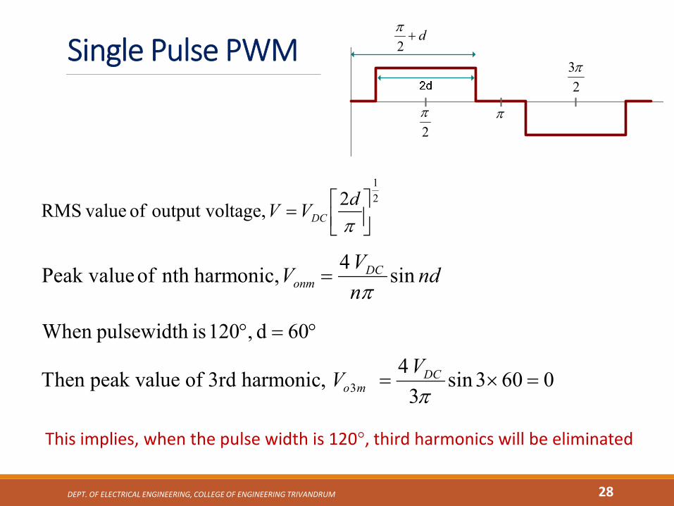
Single Pulse PWM
DEPT. OF ELECTRICAL ENGINEERING, COLLEGE OF ENGINEERING TRIVANDRUM 28
2
d2
2
3
2
1
2 tage,output vol of valueRMS
dVV DC
ndn
VV DConm sin
4 harmonic,nth of Peak value
This implies, when the pulse width is 120°, third harmonics will be eliminated
60d ,120 is pulsewidthWhen
3
4Then peak value of 3rd harmonic, sin 3 60 0
3 DC
o m
VV

Multiple Pulse PWM
DEPT. OF ELECTRICAL ENGINEERING, COLLEGE OF ENGINEERING TRIVANDRUM 29
1
2
RMS value of output voltage,
p
DC
N PV V
Comparator
Carrier Wave
Square Wave
Np = number of pulses in a half cycle
P = pulse width
Sine PWM
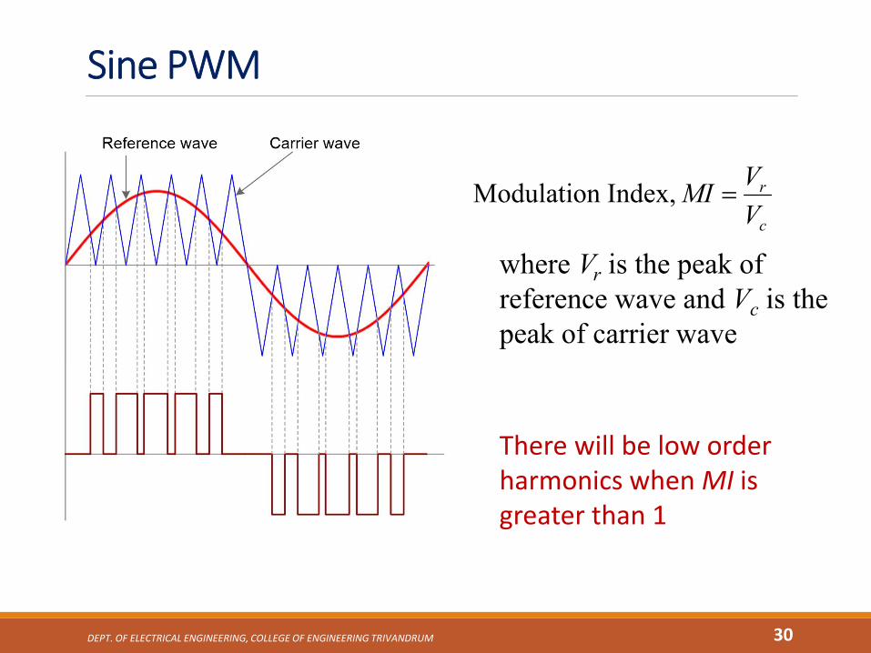
DEPT. OF ELECTRICAL ENGINEERING, COLLEGE OF ENGINEERING TRIVANDRUM 30
c
r
V
VMI Index, Modulation
where Vr is the peak of reference wave and Vc is the peak of carrier wave
There will be low order harmonics when MI is greater than 1
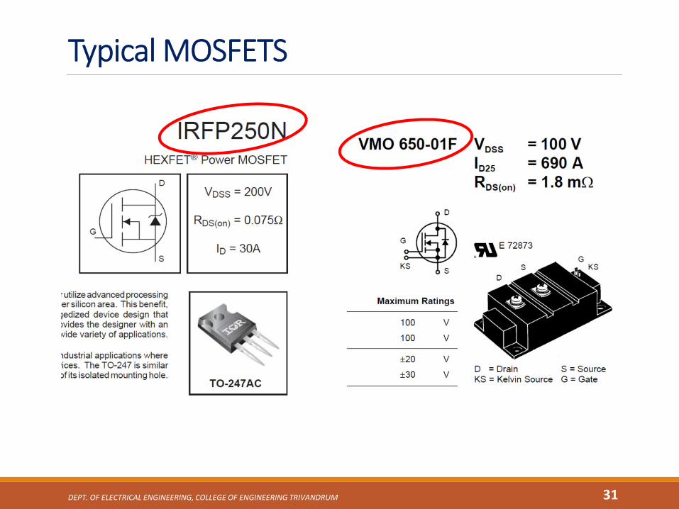
Typical MOSFETS
DEPT. OF ELECTRICAL ENGINEERING, COLLEGE OF ENGINEERING TRIVANDRUM 31

Typical IGBTs
DEPT. OF ELECTRICAL ENGINEERING, COLLEGE OF ENGINEERING TRIVANDRUM 32