Power Modeling and Characteristics of Field Programmable...
13
1712 IEEE TRANSACTIONS ON COMPUTER-AIDED DESIGN OF INTEGRATED CIRCUITS AND SYSTEMS, VOL. 24, NO. 11, NOVEMBER 2005 Power Modeling and Characteristics of Field Programmable Gate Arrays Fei Li, Member, IEEE, Yan Lin, Student Member, IEEE, Lei He, Member, IEEE, Deming Chen, and Jason Cong Abstract—This paper studies power modeling for field program- mable gate arrays (FPGAs) and investigates FPGA power char- acteristics in nanometer technologies. Considering both dynamic and leakage power, a mixed-level power model that combines switch-level models for interconnects and macromodels for look- up tables (LUTs) is developed. Gate-level netlists back-annotated with postlayout capacitances and delays are generated and cycle- accurate power simulation is performed using the mixed-level power model. The resulting power analysis framework is named as fpgaEVA-LP2. Experiments show that fpgaEVA-LP2 achieves high fidelity compared to SPICE simulation, and the absolute error is merely 8% on average. fpgaEVA-LP2 can be used to examine the power impact of FPGA circuits, architectures, and CAD algorithms, and it is used to study the power characteristics of existing FPGA architectures in this paper. It is shown that interconnect power is dominant and leakage power is significant in nanometer technologies. In addition, tuning cluster and LUT sizes lead to 1.7× energy difference and 0.8× delay difference between the resulting min-energy and min-delay FPGA architectures, and FPGA area and power are reduced at the same time by tuning the cluster and LUT sizes. The existing commercial architectures are similar to the min-energy (and min-area at the same time) architecture according to this study. Therefore, innovative FPGA circuits, architectures, and CAD algorithms, for example, consid- ering programmable power supply voltage, are needed to further reduce FPGA power. Index Terms—FPGA architecture, FPGA power model, power characteristics. I. I NTRODUCTION P OWER has become an increasingly important design con- straint in nanometer technologies. Field programmable gate arrays (FPGAs) are known to be less power efficient than application-specific integrated circuits (ASICs) because a large number of transistors are used to provide field programmability. For example, [1] compared an 8-bit adder implemented in a Xilinx XC4003A FPGA with the same adder implemented in a fully customized complementary metal oxide semiconductor (CMOS) ASIC, and showed a 100× difference in energy con- sumption (4.2 mW/MHz at 5 V for FPGA versus 5.5 µW/MHz at 3.3 V for ASIC counterpart). Therefore, it is important to study power modeling and reduction for nanometer FPGAs. Manuscript received July 10, 2003; revised May 20, 2004 and December 13, 2004. This work was supported in part by NSF CAREER Award CCR-0401682 and NSF Grant CCR-0306682. This paper was recommended by Associate Editor M. Pedram. F. Li, Y. Lin, and L. He are with the Department of Electrical Engineering, University of California, Los Angeles, CA 90095 USA. D. Chen and J. Cong are with the Department of Computer Science, University of California, Los Angeles, CA 90095 USA. Digital Object Identifier 10.1109/TCAD.2005.852293 There is limited published work about FPGA power mod- eling and power characteristics. Kussey and Rabaey [1] used a Xilinx XC4003A FPGA test board to measure power and reported a power breakdown for FPGA components. Shang et al. [2] analyzed the dynamic power for Xilinx Virtex-II FPGA family based on measurement and simulation. Weiß et al. [3] presented the power consumption for Xilinx Virtex architecture using an emulation environment. Tuan and Lai [4] studied the leakage power of Xilinx architectures. The afore- mentioned work was all carried out for specific FPGA architec- tures. Parameterized power models were proposed for generic FPGA architectures in [5] and an early version [6] of this paper. However, both [5] and [6] oversimplified the models for short- circuit and leakage power, and verification by measurement or circuit-level simulation was not reported in [5] and [6]. This paper first develops a mixed-level power model more accurate than those in [5] and [6] for parameterized FPGA ar- chitectures. Cluster-based logic blocks and island-style routing structures are assumed. One logic block is a cluster of look- up tables (LUTs) with the cluster size N (i.e., the number of LUTs inside one cluster) and the LUT size k (i.e., the number of inputs to the LUT) as the architectural parameters. Logic blocks are embedded into the routing resources as logic “islands” and segmented wires are used to connect these logic “islands.” This parameterized FPGA architecture is general enough to cover the architectural features of most commercial FPGAs such as [7] and [8]. The proposed new power model considers both dynamic and leakage power, and combines switch-level mod- els for interconnects and macromodels for logic cells. Gate- level netlists back-annotated with postlayout capacitances and delays are generated, and cycle-accurate power simulation is performed. A detailed delay model is used for glitch power analysis and short-circuit power is modeled as a function of sig- nal transition time. Experiments show that the proposed power model achieves high fidelity compared to SPICE simulation, and the absolute error is around 8% on average. The resulting power analysis framework is named as fpgaEVA-LP2 and is applied to evaluating the power character- istics of existing FPGA architectures in 100 nm technology. It is shown that interconnect power is dominant and leakage power is significant in nanometer technologies. In addition, tuning cluster and LUT sizes lead to 1.7× energy difference and 0.8× delay difference between the resulting min-energy and min- delay FPGA architectures, and FPGA area and power can be reduced at the same time by tuning cluster and LUT sizes. The existing commercial architectures are similar to the min-energy (and min-area at the same time) architecture according to this study. Therefore, innovative FPGA circuits, architectures, 0278-0070/$20.00 © 2005 IEEE
-
Upload
nguyenquynh -
Category
Documents
-
view
231 -
download
0
Transcript of Power Modeling and Characteristics of Field Programmable...

1712 IEEE TRANSACTIONS ON COMPUTER-AIDED DESIGN OF INTEGRATED CIRCUITS AND SYSTEMS, VOL. 24, NO. 11, NOVEMBER 2005
Power Modeling and Characteristics of FieldProgrammable Gate Arrays
Fei Li, Member, IEEE, Yan Lin, Student Member, IEEE, Lei He, Member, IEEE, Deming Chen, and Jason Cong
Abstract—This paper studies power modeling for field program-mable gate arrays (FPGAs) and investigates FPGA power char-acteristics in nanometer technologies. Considering both dynamicand leakage power, a mixed-level power model that combinesswitch-level models for interconnects and macromodels for look-up tables (LUTs) is developed. Gate-level netlists back-annotatedwith postlayout capacitances and delays are generated and cycle-accurate power simulation is performed using the mixed-levelpower model. The resulting power analysis framework is namedas fpgaEVA-LP2. Experiments show that fpgaEVA-LP2 achieveshigh fidelity compared to SPICE simulation, and the absoluteerror is merely 8% on average. fpgaEVA-LP2 can be used toexamine the power impact of FPGA circuits, architectures, andCAD algorithms, and it is used to study the power characteristicsof existing FPGA architectures in this paper. It is shown thatinterconnect power is dominant and leakage power is significant innanometer technologies. In addition, tuning cluster and LUT sizeslead to 1.7× energy difference and 0.8× delay difference betweenthe resulting min-energy and min-delay FPGA architectures, andFPGA area and power are reduced at the same time by tuningthe cluster and LUT sizes. The existing commercial architecturesare similar to the min-energy (and min-area at the same time)architecture according to this study. Therefore, innovative FPGAcircuits, architectures, and CAD algorithms, for example, consid-ering programmable power supply voltage, are needed to furtherreduce FPGA power.
Index Terms—FPGA architecture, FPGA power model, powercharacteristics.
I. INTRODUCTION
POWER has become an increasingly important design con-straint in nanometer technologies. Field programmable
gate arrays (FPGAs) are known to be less power efficient thanapplication-specific integrated circuits (ASICs) because a largenumber of transistors are used to provide field programmability.For example, [1] compared an 8-bit adder implemented in aXilinx XC4003A FPGA with the same adder implemented ina fully customized complementary metal oxide semiconductor(CMOS) ASIC, and showed a 100× difference in energy con-sumption (4.2 mW/MHz at 5 V for FPGA versus 5.5 µW/MHzat 3.3 V for ASIC counterpart). Therefore, it is important tostudy power modeling and reduction for nanometer FPGAs.
Manuscript received July 10, 2003; revised May 20, 2004 and December 13,2004. This work was supported in part by NSF CAREER Award CCR-0401682and NSF Grant CCR-0306682. This paper was recommended by AssociateEditor M. Pedram.
F. Li, Y. Lin, and L. He are with the Department of Electrical Engineering,University of California, Los Angeles, CA 90095 USA.
D. Chen and J. Cong are with the Department of Computer Science,University of California, Los Angeles, CA 90095 USA.
Digital Object Identifier 10.1109/TCAD.2005.852293
There is limited published work about FPGA power mod-eling and power characteristics. Kussey and Rabaey [1] useda Xilinx XC4003A FPGA test board to measure power andreported a power breakdown for FPGA components. Shanget al. [2] analyzed the dynamic power for Xilinx Virtex-IIFPGA family based on measurement and simulation. Weißet al. [3] presented the power consumption for Xilinx Virtexarchitecture using an emulation environment. Tuan and Lai [4]studied the leakage power of Xilinx architectures. The afore-mentioned work was all carried out for specific FPGA architec-tures. Parameterized power models were proposed for genericFPGA architectures in [5] and an early version [6] of this paper.However, both [5] and [6] oversimplified the models for short-circuit and leakage power, and verification by measurement orcircuit-level simulation was not reported in [5] and [6].
This paper first develops a mixed-level power model moreaccurate than those in [5] and [6] for parameterized FPGA ar-chitectures. Cluster-based logic blocks and island-style routingstructures are assumed. One logic block is a cluster of look-up tables (LUTs) with the cluster size N (i.e., the number ofLUTs inside one cluster) and the LUT size k (i.e., the number ofinputs to the LUT) as the architectural parameters. Logic blocksare embedded into the routing resources as logic “islands” andsegmented wires are used to connect these logic “islands.” Thisparameterized FPGA architecture is general enough to coverthe architectural features of most commercial FPGAs such as[7] and [8]. The proposed new power model considers bothdynamic and leakage power, and combines switch-level mod-els for interconnects and macromodels for logic cells. Gate-level netlists back-annotated with postlayout capacitances anddelays are generated, and cycle-accurate power simulation isperformed. A detailed delay model is used for glitch poweranalysis and short-circuit power is modeled as a function of sig-nal transition time. Experiments show that the proposed powermodel achieves high fidelity compared to SPICE simulation,and the absolute error is around 8% on average.
The resulting power analysis framework is named asfpgaEVA-LP2 and is applied to evaluating the power character-istics of existing FPGA architectures in 100 nm technology. It isshown that interconnect power is dominant and leakage poweris significant in nanometer technologies. In addition, tuningcluster and LUT sizes lead to 1.7× energy difference and 0.8×delay difference between the resulting min-energy and min-delay FPGA architectures, and FPGA area and power can bereduced at the same time by tuning cluster and LUT sizes. Theexisting commercial architectures are similar to the min-energy(and min-area at the same time) architecture according tothis study. Therefore, innovative FPGA circuits, architectures,
0278-0070/$20.00 © 2005 IEEE

LI et al.: POWER MODELING AND CHARACTERISTICS OF FIELD PROGRAMMABLE GATE ARRAYS 1713
Fig. 1. Basic logic element (BLE).
Fig. 2. Cluster-based logic block.
and CAD algorithms, for example, applying programmablepower supply, are needed to further reduce FPGA power.fpgaEVA-LP2 has been employed in a few recent studies onFPGA power reduction [9]–[13].
The paper is organized as follows. Section II introduces back-ground knowledge. Section III discusses the proposed mixed-level power model. Section IV introduces the power analysisframework fpgaEVA-LP2 and studies power characteristics ofthe existing FPGA architectures. Section V concludes the paperwith discussion of recent research progress for FPGA powerreduction. An extended abstract of this paper was presentedin [13].
II. FPGA BACKGROUND
A. Candidate Architectures
An FPGA architecture is mainly defined by its logic blockand routing structure. By varying the architectural parametersfor logic blocks and routing structure, one can create manydifferent FPGA architectures. LUT-based FPGAs are assumed,where the basic logic element (BLE) (see Fig. 1) consists of onek-input look-up table (k-LUT) and one flip-flop. The output ofthe k-LUT can be programmed to be either registered or un-registered. Previous work [14] has shown that a different LUTinput number k leads to a different tradeoff between FPGAarea and performance. It will be interesting to investigate howthe LUT input number k affects FPGA power consumption. NBLEs can further form a cluster-based logic block as shownin Fig. 2. The cluster inputs and outputs are fully connectedto the inputs of each LUT [15]. Cluster size N is another im-portant architectural parameter that affects FPGA performanceand power.
Routing structure is critical to FPGA designs because routingwires consume a large portion of the total FPGA area [16] and
Fig. 3. Island-style routing structure.
Fig. 4. Clock network.
power [1]. This paper assumes island-style routing that is usedin most commercial FPGAs such as [7], [8] and [17]. The logicblocks are connected by a two-dimensional (2-D) mesh-likeinterconnect structure, and horizontal and vertical routing chan-nels are connected by programmable switch blocks. Fig. 3presents a simplified view of an example island-style routingstructure, where half of the routing tracks consist of length-1wires (wires spanning one logic block) and the other halfconsist of length-2 wires. Programmable routing switches areeither pass transistors or tristate buffers. There are also switches(called connection blocks) connecting the wire segments tothe logic block inputs and outputs. Betz et al. [18] define therouting architectural parameters including channel width (W ),switch block flexibility (Fs—the number of wires to whicheach incoming wire can connect in a switch block), connectionblock flexibility (Fc—the number of wires in each channelto which a logic block input or output pin can connect) andsegmented wire lengths.
In addition to logic block and routing architectures, clockdistribution structure is another aspect in FPGA designs. Asimple H-tree structure is assumed for FPGA clock networks(see Fig. 4). A tile is a cluster-based logic block with clustersize N . Each clock tree buffer in the H-tree has two branches.Clock tree buffers in the H-tree are considered to be clocknetwork resources. Chip area, tile size, and routing channelwidth determine the clock tree depth and the branch lengths.Commercial FPGA architectures usually have multiple clock

1714 IEEE TRANSACTIONS ON COMPUTER-AIDED DESIGN OF INTEGRATED CIRCUITS AND SYSTEMS, VOL. 24, NO. 11, NOVEMBER 2005
networks. For example, Altera Stratix [8] has 16 global clocknetworks and 16 regional clock networks. Each global clocknetwork drives through the entire device, and each regionalclock network provides clock signals to one quadrant of thechip. In this paper, it is simply assumed that there are fourclock networks, and each of them provides a clock signal tothe whole chip. More realistic clock networks can be modeledand studied with details of clock network design.
B. Area Model
The area model in fpgaEVA-LP2 is based on the technology-scalable area model implemented in VPR [18]. Basically, thenumber of minimum-width transistor areas required to im-plement a specific FPGA architecture is counted. By usingthe number of minimum-width transistor areas instead of thenumber of microsquares, this area model can be easily appliedto future technologies.
C. Delay Model
The delay model in fpgaEVA-LP2 uses delay values obtainedby SPICE simulations in the predictive 100 nm CMOS technol-ogy [19]. BSIM4 SPICE model is used in the circuit simulation.Table I shows some key model parameters for the proposed de-vice and interconnect model. Various circuit paths inside a logicblock are simulated and path delays are precharacterized. Fig. 5presents the schematic of a cluster-based logic block, which isextended from the schematics presented in [14]. Table II showssome key delay values corresponding to the paths in Fig. 5 (onlydata for k = 4 are shown in the table). Note that the delay ofpath C → E is larger than the delay of path C → D. This is be-cause path C → E is for the BLE sequential mode, and its delayincludes both LUT delay and setup time of the flip-flop. PathC → D is for the BLE combinational mode and the flip-flop isbypassed. The area model in VPR is further used to estimateFPGA layout geometry by assuming the tile-based layout [18].The resistance and capacitance of wires in the routing channelsare estimated by using the proposed interconnect model. Passtransistors connecting different wire segments are modeledby the equivalent resistance and capacitance. Elmore delayis then calculated for the interconnect resistance–capacitance(RC) trees in a given netlist. The details of interconnect delaycalculation are discussed in Section IV-A.
III. MIXED-LEVEL POWER MODEL
A. Overview
There are three power sources in FPGAs, namely: 1) switch-ing power; 2) short-circuit power; and 3) static power. The firsttwo types of power together are called dynamic power, andthey can only occur when a signal transition happens. Thereare two types of signal transitions. 1) Functional transition isthe necessary signal transition to perform the required logicfunctions between two consecutive clock ticks. 2) Spurioustransition or glitch is the unnecessary signal transition due tothe unbalanced path delays to the inputs of a gate. Glitch powercan be a significant portion of the dynamic power. The thirdtype of power, static power, is the power consumed when there
TABLE IDEVICE AND INTERCONNECT MODEL IN OUR SPICE SIMULATION
AT 100 nm TECHNOLOGY
is no signal transition for a gate or a circuit module. As thetechnology advances to feature size of 100 nm and below, staticpower will become comparable to dynamic power. The differentpower sources are summarized in columns 1–3 of Table III.
To consider the above power sources, both switch-level mod-el and macromodel are developed as summarized in columns 4and 5 of Table III. A switch-level model uses formulas andextracted parameters, such as capacitance and resistance, tomodel the power consumption related to signal transitions. Amacromodel precharacterizes a circuit module using SPICEsimulation and builds an LUT for power values. In the follow-ing, the dynamic power models are discussed, which includethe switch-level model for interconnects and clock networksas presented in Section III-B1 and the macromodels for LUTsas discussed in Section III-B2. The transition density andglitch analysis applicable to both interconnects and LUTs arediscussed in Section III-B3. Section III-C then introduces theproposed static power model and Section III-D summarizes theoverall power calculation.
B. Dynamic Power Model
1) Switch-Level Model for Interconnects: One type of dy-namic power, switching power Psw, is usually modeled by thefollowing formula
Psw = 0.5fV 2dd
n∑i=1
CiEi (1)
where n is the total number of nodes, f is the clock frequency,Vdd is the supply voltage, Ci is the load capacitance for node i,and Ei is the transition density for node i. To apply this switch-level model directly, the capacitance Ci has to be extracted andthe transition density Ei estimated for each circuit node. How-ever, (1) cannot take into account internal nodes in a complexcircuit module such as the LUTs. A flattened netlist is neededto apply (1), which results in the loss of computational ef-ficiency. Furthermore, (1) only considers full swings eitherfrom Vdd to GND or GND to Vdd. Glitches due to small delaydifferences at the gate inputs may have partial swings thatcannot be correctly modeled by (1). To achieve computationalefficiency, the switch-level model is only applied to intercon-nects as well as buffers in clock networks. Macromodels aredeveloped for LUTs and the transition density of LUTs is usedto calculate their dynamic power, which will be discussed inSection III-B2. To correctly model glitches with partial swing
LI et al.: POWER MODELING AND CHARACTERISTICS OF FIELD PROGRAMMABLE GATE ARRAYS 1715
Fig. 5. Schematic for a logic block.
TABLE IIKEY DELAY NUMBERS FOR PATHS IN FIG. 5 (k = 4)
TABLE IIIPOWER SOURCES AND MIXED-LEVEL POWER MODEL
at switch level, effective transition density Ei is defined, and(1) is extended as
Psw = 0.5fV 2dd
n∑i=1
CiEi. (2)
Details of Ei calculation and glitch analysis will be discussedin Section III-B3.
Short-circuit power Psc is another type of dynamic power.When a signal transition occurs at a gate output, both the pull-up and pull-down transistors can be conducting simultaneouslyfor a short period of time. Short-circuit power represents thepower dissipated via the direct current path from Vdd to GNDduring the signal transition. It is a function of the input signaltransition time and load capacitance. The short-circuit poweris modeled for interconnects and clock network at the switchlevel. Short-circuit power for LUTs is considered in theirmacromodels and will be discussed later on.
To determine the short-circuit power, interconnect buffers aresimulated with different sizes and load capacitances, and the
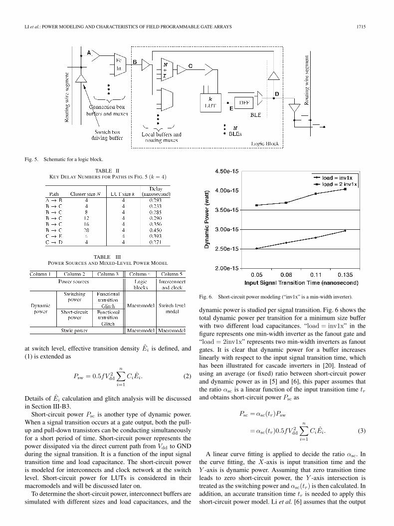
Fig. 6. Short-circuit power modeling (“inv1x” is a min-width inverter).
dynamic power is studied per signal transition. Fig. 6 shows thetotal dynamic power per transition for a minimum size bufferwith two different load capacitances. “load = inv1x” in thefigure represents one min-width inverter as the fanout gate and“load = 2inv1x” represents two min-width inverters as fanoutgates. It is clear that dynamic power for a buffer increaseslinearly with respect to the input signal transition time, whichhas been illustrated for cascade inverters in [20]. Instead ofusing an average (or fixed) ratio between short-circuit powerand dynamic power as in [5] and [6], this paper assumes thatthe ratio αsc is a linear function of the input transition time trand obtains short-circuit power Psc as
Psc = αsc(tr)Psw
= αsc(tr)0.5fV 2dd
n∑i=1
CiEi. (3)
A linear curve fitting is applied to decide the ratio αsc. Inthe curve fitting, the X-axis is input transition time and theY -axis is dynamic power. Assuming that zero transition timeleads to zero short-circuit power, the Y -axis intersection istreated as the switching power and αsc(tr) is then calculated. Inaddition, an accurate transition time tr is needed to apply thisshort-circuit power model. Li et al. [6] assumes that the output

1716 IEEE TRANSACTIONS ON COMPUTER-AIDED DESIGN OF INTEGRATED CIRCUITS AND SYSTEMS, VOL. 24, NO. 11, NOVEMBER 2005
TABLE IVVALUE OF PARAMETER α TO DETERMINE SIGNAL TRANSITION TIME
TABLE VDYNAMIC POWER OF A FOUR-LUT UNDER DIFFERENT
INPUT VECTOR PAIRS
signal transition time is twice of the buffer delay. This sim-plistic assumption was originally used in gate sizing [21], [22],and it is valid when the input signal is a step function and theoutput signal is a ramp function. SPICE is used to simulate atypical routing path in an FPGA, where a routing switch drivesa wire segment and other routing switches. It was found thatthe input signal is no longer a step function because the input isthe output of a routing switch in the previous stage. The outputsignal under a large load capacitance, which is usually the casein FPGAs, is not a perfect ramp function, and the 10–90%transition time for the output signal can be significantly largerthan twice the buffer delay. The output signal transition timetr as tr = αtbuffer is modeled, where tbuffer is the buffer delayunder load capacitance. SPICE simulation is used to determinethe parameter α for different buffer delays (see Table IV),which covers the cases of various input signal transition timeand different load capacitance.2) Macromodel for LUTs: Macromodels for LUT dynamic
power are built. Since LUTs are regularly connected in acluster-based logic block, they usually have a fixed load capac-itance. This reduces the number of dimensions of the powerLUT in the proposed macromodel. However, as shown inTable V, different input vector pairs (v1 → v2) for an LUTlead to different levels of dynamic power. SPICE simulationis used with randomly generated input vectors to obtain theaverage dynamic power per access to the LUT, and thereforecompress the complete power table into one power value as-suming equal occurrence probability for all input vectors. Thenumber of vectors is decided so that the change of averagepower is negligible by increasing the number of vectors, anda few hundreds of input vectors are used in the experiments.The power values for LUTs with different sizes are stored,and the access transition density for LUTs is used to cal-culate their dynamic power. The proposed power model issimilar to that in the architectural-level microprocessor poweranalysis tool Wattch [23] in the sense that both assume thatall the input vectors have an equal occurrence probabilityand therefore the (average) dynamic power is independent oflogic vectors.1
1To consider the different switching probability in different applications,methods such as the input vector clustering [24] can be employed to improve thepower model in the future. In addition, we will study how to find representativeinput vectors for power characterization.
Fig. 7. Glitches at a circuit node.
Fig. 8. RC circuit model.
3) Transition Density and Glitch Analysis: A recent workon FPGA power modeling [5] uses Boolean difference to cal-culate the transition density. However, it is difficult for Booleandifference to precisely capture the spatial and temporal signalcorrelations among circuit nodes [25]. The gate-level cycle-accurate simulation is used to calculate the transition density.Assuming that primary inputs of a circuit have a signal proba-bility of 0.5 and transition probability of 0.85, a large number ofrandom input vectors are generated to simulate the circuit. Twothousand random vectors are used in this paper. To considersequential circuits, these 2000 random vectors for real primaryinputs are divided into 20 vector sequences, with the uniformsequence length of 100. At the beginning of the simulation foreach vector sequence, initial states for pseudo primary inputsare randomly generated, i.e., the outputs of flip-flops, with asignal probability of 0.5 and the next state is calculated in everycycle of the vector sequence.
Glitches may occur at a gate output when the incoming sig-nals reach the gate inputs at different times due to unbalancedpath delays. Fig. 7 illustrates this case. When inputs a and b ofthe AND gate do not switch at the same time, a glitch (spurioustransition) is generated at the output before it finally stabilizes.Although the interconnect buffers have only one input, theymay propagate the glitches and may also consume glitch power.Glitches are not always full swings from Vdd to GND or GNDto Vdd. When t1 and t2 in Fig. 7 are close enough to eachother, the maximum voltage level of the glitch can be lowerthan Vdd due to the nonzero signal transition time. Clearly,dynamic power of such a glitch is smaller than that of a fullswing.
To consider the partial swings in the proposed power model,a gate with the simple RC circuit is modeled as shown in Fig. 8.R is the effective pull-up transistor resistance and C is the

LI et al.: POWER MODELING AND CHARACTERISTICS OF FIELD PROGRAMMABLE GATE ARRAYS 1717
load capacitance. The current i(t) charges the load capacitanceC and the gate output V (t) has a rising transition. Let V1 be theinitial value of V (t) and V2 be the maximum voltage that therising transition can reach. Then
CdV (t)
dt= i(t). (4)
Energy consumption Esw of the resistance R is calculated asfollows
Esw(V1 → V2) =
t2∫
t1
i2(t)Rdt
=
t2∫
t1
i(t) (Vdd − V (t)) dt
=
V2∫
V1
C (Vdd − V (t)) dV (t)
=C
2(V1 − V2)(V1 + V2 − 2Vdd).
The effective transition number for rising signal transitions isdefined as
Ni(rising) =(V1 − V2)(V1 + V2 − 2Vdd)
V 2dd
Ni (5)
where Ni is the transition number for node i including bothfunctional transitions and glitches. Note that Ni becomesequal to Ni when only full swing is considered. Similarly,the formula for power dissipation of a falling signal tran-sition can be derived and the effective transition number isdefined as
Ni(falling) =V 2
2 − V 21
V 2dd
Ni. (6)
Switching power considering partial swings is then calcu-lated as
Psw = 0.5fV 2dd
n∑i=1
CiEi (7)
Ei =Ni
cycles(8)
where Ei is the effective transition density and Ni is the totaleffective transition number in all the simulation cycles. Whenthe input glitch is very narrow, the output glitch will have avery small amplitude and hence does not contribute to the totaleffective transition number. In this case, the proposed glitchpower model naturally filters out narrow glitches, known to bethe effect of the inertial gate delay. Note that effective transitiondensity is also used in the macromodels for LUTs to calculateLUT dynamic power considering partial swings.
C. Static Power
Static power is also called leakage power. According to[26], the leakage power in a nanoscale CMOS device includesreverse-biased leakage, subthreshold leakage power, drain-induced barrier lowering leakage, gate tunneling leakage, gate-induced drain leakage, etc. The total leakage power of a logicgate is a function of technology, temperature, static input vector,and stack effect of the gate type. The recent FPGA powermodel [5] calculates the subthreshold leakage current by using aformula. However, they simply assume the gate-source voltagefor all the OFF transistors to be half of the threshold voltage,which is usually not true when stack effect is considered. SPICEsimulation is used to obtain the leakage power due to variousdevice level mechanisms. The average leakage power assumingall the input vectors have the same probability of occurrenceis used in the proposed power model. Because “gate boosting”is applied [18] to interconnect switches in the routing channelsand compensate the logic “1” degradation of negative channelmetal oxide semiconductor (NMOS) pass transistor,2 either Vdd
or GND is applied as the input signals in the SPICE simulationfor global interconnect leakage power. The local interconnectmultiplexers inside logic blocks have not adopted gate boostingin the proposed circuit design. Therefore, the proposed powermodel for local interconnects gives larger leakage power dueto level degradation. Since the number of all possible inputvectors increases exponentially with the number of inputs forLUTs, it is infeasible to try all the input vectors and get theaverage leakage power. Different input vectors are mapped intoa few typical vectors with representative Hamming distancesand SPICE simulation is performed only for these typical vec-tors to build macromodels. SPICE simulation is performed forLUT sizes ranging from three to seven and buffers of varioussizes in global/local interconnects, and then static power macro-models are built.
D. Overall Power Calculation
The power calculation using the mixed-level power modelis summarized in Fig. 9. A gate-level netlist (the BC-netlistdiscussed in Section IV-A) back-annotated with gate capac-itance and wire capacitance is used to begin with. Randominput vectors are generated according to the specified signalprobability and transition probability. A cycle-accurate simu-lator with glitch analysis is used to calculate the power foreach component in an FPGA. During each simulation cycle,the effective transition number for the output signal of aninterconnect buffer or access signal to an LUT is counted,and then the dynamic power in that cycle is calculated andadded. Since leakage power always exists, even if there is asignal transition, the leakage power for interconnect buffersis also added. The leakage power for LUTs is not addedin that cycle because the dynamic power macromodel basedon SPICE simulation has already taken that into account. Ifthere is no signal transition for an interconnect buffer or no
2Other techniques such as weak-pull-up keeper transistor can also be used toavoid logic “1” degradation in NMOS pass transistor.

1718 IEEE TRANSACTIONS ON COMPUTER-AIDED DESIGN OF INTEGRATED CIRCUITS AND SYSTEMS, VOL. 24, NO. 11, NOVEMBER 2005
Fig. 9. Overall power calculation.
Fig. 10. Comparison between SPICE simulation and cycle-accurate powersimulation with both previous power model and the proposed new power model.
access to an LUT, the static power is calculated and added.For clock power, the dynamic and leakage power for clocknetwork buffers is calculated. The above power consumptionin each cycle is accumulated until all the simulation vectorsare finished.
The proposed mixed-level power model is similar to that in[6], but we use more detailed modeling for short-circuit andstatic power. Before applying the new power model to estimatepower consumption at full-chip level, we verify the fidelity andaccuracy of this cycle-accurate power simulation compared toSPICE simulation. Because it is impossible to carry out SPICEsimulation for large circuits at full-chip level, we choose fivecircuits from the MCNC benchmark set so that the circuitsize is within the capability of SPICE simulation. They aremapped into LUTs with an LUT size of four and packed intoclusters with a cluster size of four. The largest circuit occupiessix clusters, and the smallest circuit occupies two clusters.Fig. 10 compares the power model from [6] and the new powermodel in this paper to SPICE simulation. The power model in[6] achieves high fidelity but consistently underestimates thetotal FPGA power. With the proposed new power model, highfidelity is maintained and the absolute error is reduced to 8%on average for the five circuits.
Fig. 11. FPGA power analysis framework (fpgaEVA-LP2).
IV. POWER ANALYSIS FRAMEWORK AND FPGAPOWER CHARACTERISTICS
A. Power Analysis Framework fpgaEVA-LP2
Power analysis framework fpgaEVA-LP2 is built using thenew power model and show the overall analysis flow in Fig. 11.For a given circuit, SIS is used [27] to perform the technology-independent logic optimization and Flowmap [28] in RASP[29] is used to conduct the technology mapping. The physicaldesign in VPR [18] is then carried out, including timing-drivenpacking, placement, and routing. VPR generates FPGA arraywhose size just fits the given benchmark circuit. Further, VPRdecides the routing channel width W as W = 1.2Wmin, andWmin is the minimum channel width required to route the givenbenchmark successfully. This means that VPR is customizingthe FPGA for each benchmark so that it reflects the “low-stress”routing situation that usually occurs in commercial FPGAs for“average” circuits. The same flow is applied in fpgaEVA-LP2and the BC-netlist back-annotated with postlayout resistanceand capacitance is generated. The BC-netlist is further used toperform timing and power analysis.
Both delay and capacitance values in the BC-netlist are ex-tracted for the elements of logic blocks and interconnects. Theoriginal VPR only cares about the delay from the source to eachsink in every routing net. The intermediate routing buffers donot appear in the VPR timing graph. However, load capacitanceis needed for routing buffers to calculate their power consump-tion. As shown in Fig. 12, the routing buffers usually separate arouting net into several parts. Each part of the net may consistof one or several wire segments that are connected by eitherpass-transistors or buffers. For example, buffer X in Fig. 12 hasthree fanout branches. Branch b1 has only one wire segment,

LI et al.: POWER MODELING AND CHARACTERISTICS OF FIELD PROGRAMMABLE GATE ARRAYS 1719
Fig. 12. Example for wire delay calculation (delay values are innanoseconds).
TABLE VILOGIC BLOCK AND ROUTING ARCHITECTURES STUDIED
IN OUR EXPERIMENTS
while branch b2 and b3 have three and two wire segments, re-spectively. Capacitance extraction is carried out in a wire-by-wire fashion and all the capacitances of the buffer fanoutbranches were lumped into its load capacitance. Fig. 12 alsoshows how the delay along each fanout branch for bufferX is modeled. Taking branch b2 as an example, RC delaysare calculated segment-by-segment considering attached pass-transistor switches and finally obtain the delay from the inputof buffer X to the input of buffer Y .
Initially, the basic circuit elements in the BC-netlist are justLUTs. The buffers used in the local wires are then insertedinside logic blocks or those used in the routing tracks. There-fore, a one-to-one correspondence is maintained between eachbasic circuit element (including interconnect buffers) and eachextracted delay/capacitance value. The logic function of thebasic circuit elements and the delay between two connectedbasic circuit elements are used in switching activity calculationand glitch analysis. The extracted capacitances in the BC-netlistare used for power calculation.
The proposed power analysis framework fpgaEVA-LP2 canbe used to investigate the impact of circuits, architectures, andCAD algorithms upon FPGA power dissipation. In the follow-ing, fpgaEVA-LP2 is used to study the power characteristicsof existing FPGA architectures. Table VI presents the FPGAarchitectures studied in the experiments. A suite of logic blockarchitectures with different cluster size N and LUT size k isexamined. For all logic block architectures, the same routingarchitecture is used as the default one in VPR, where wiresegmentation length is four logic blocks, and 50% of routingswitches are tristate buffers and the others are pass transistors.In all the experiments, 0.5 W is used for the logic blockinput flexibility Fc(input) and 0.25 W for the logic blockoutput flexibility Fc(output), where W is the channel width
Fig. 13. VPR random seed versus FPGA delay and energy for circuit s38584(cluster size = 10, LUT size = 4, default routing architecture in VPR).
in track number. The FPGA delay and power are presentedin geometric mean over 20 largest MCNC benchmarks. Thepower breakdown is presented in the arithmetic average over20 benchmarks.
B. Impact of Random Seed in VPR
In the proposed power analysis framework fpgaEVA-LP2,VPR [18] is used to place and route benchmark circuits. Theplacement tool in VPR applies simulated annealing algorithmwith a specified initial random seed. A different seed can leadto a different placement and routing result, and it may furtheraffect the circuit delay and power. To study the impact of VPRrandom seed, the same benchmark circuit is placed and routedten times, and a different VPR random seed is used each time.The delay and power variation for these VPR runs are theninvestigated. Fig. 13 shows the result for a large circuit s38584.The seed value is labeled beside each data point. The criticalpath delay variation is 12% (from 10.60 to 11.87 ns) and theenergy variation is 6% (from 7.021 to 7.441 nJ/cycle). Further-more, Table VII summarizes the delay and energy variation forthe MCNC benchmark set with cluster size 10 and LUT size 4.On average, the delay variation is 22.08% and the powervariation is 15.33%. Note that the min-delay VPR run oftenconsumes lower energy. Considering the relatively larger delayvariation due to VPR random seeds, the min-delay VPR run isalways used for each benchmark circuit among all VPR seeds,and FPGA power characteristics are presented for the rest ofthe paper.
C. Transition Density, Glitch Power, and Short-Circuit Power
Since glitch power is due to the spurious transitions in acircuit, the transition density calculation in the power simu-lation should consider these spurious transitions. The averageeffective transition density per circuit node is presented fortwo large benchmark circuits in Table VIII. “bigkey” is acombinational circuit and “s38584” is a sequential circuit. Thetransition density value without glitch analysis is comparedto that with glitch analysis. Clearly, the calculation without

1720 IEEE TRANSACTIONS ON COMPUTER-AIDED DESIGN OF INTEGRATED CIRCUITS AND SYSTEMS, VOL. 24, NO. 11, NOVEMBER 2005
TABLE VIIFPGA ENERGY AND DELAY VARIATION DUE TO VPR RANDOM SEED FOR 20 MCNC BENCHMARK CIRCUITS
(CLUSTER SIZE = 10, LUT = 4, DEFAULT ROUTING ARCHITECTURE)
TABLE VIIIAVERAGE TRANSITION DENSITY PER CIRCUIT NODE
(CLUSTER SIZE = 8, LUT = 4)
glitch analysis underestimates the transition density. The av-erage percentage of glitch power is further presented, foreach LUT size k, over a series of benchmarks in Table IX.The experiments show that glitch power is an important partof total FPGA power, and its portion can be as large as 19%in the experiments. The short-circuit power depends on bothswitching activity and signal transition time. It has been foundthat the signal transition time in the FPGA design is large andshort-circuit power is a significant power component. Table Xpresents the various power components for global interconnectsand illustrates that both short-circuit and leakage power aresignificant and vary a lot between different circuits.
D. Impact of Logic Block Architecture
In this section, the impact of logic block architecture (i.e.,LUT size and cluster size) on delay and power is studied.Fig. 14 shows the critical path delay for different cluster andLUT sizes. In general, a larger LUT size leads to smallercritical path delay because the number of LUTs in series onthe critical path decreases. However, for large cluster sizesuch as size 12, the critical path delay increases as the LUTsize increases (see LUT sizes 4–7). This is because the delaythrough a cluster increases greatly for large cluster size.
TABLE IXGLITCH POWER (CLUSTER SIZE = 8)
Since interconnects are usually the dominant FPGA re-sources, FPGA interconnect energy is further shown in Fig. 15.As the LUT size increases, the total number of LUT inputpins in a cluster increases and the number of local interconnectbuffers and multiplexers (MUXes) also increases in order tofully connect these LUTs. This leads to the increase of localinterconnect energy. On the other hand, the global intercon-nect energy decreases when the LUT size increases. This isbecause fewer LUTs and clusters are needed to implementthe given circuit, which leads to smaller FPGA array sizeand less global interconnect resource. For the same clustersize, the results show that LUT size 4 leads to the minimuminterconnect energy. Cluster size also affects the interconnectenergy. A larger cluster size increases local interconnect en-ergy but reduces global interconnect energy. Fig. 15 showsthat the total interconnect energy usually increases as clustersize increases, but the energy difference is not very largeexcept for seven-input LUTs. Leakage power in nanometertechnology is significant, and the FPGA leakage energy ispresented in Fig. 16. Leakage energy is mainly decided bytotal FPGA resources including logic blocks and intercon-nects. Since it has been shown in [14] that LUT size 4achieves the highest total-area efficiency, it is expected thatLUT size 4 also achieves minimum leakage energy, and this isverified in Fig. 16. Considering all the power dissipation com-ponents, total FPGA energy is presented in Fig. 17. Clearly, theresults for all the cluster sizes consistently show that the LUT

LI et al.: POWER MODELING AND CHARACTERISTICS OF FIELD PROGRAMMABLE GATE ARRAYS 1721
TABLE XGLOBAL INTERCONNECT POWER FOR TWO CIRCUITS (CLUSTER SIZE = 8, LUT = 4,)
Fig. 14. Impact of logic block architecture on critical path delay.
Fig. 15. Impact of logic block architecture on FPGA interconnect energy.
size 4 gives the lowest total FPGA energy compared to otherLUT sizes.
Fig. 18 further plots energy and delay for all logic blockarchitectures and shows the tradeoff between FPGA power andperformance. The X-axis is critical path delay and the Y -axisis total FPGA energy. Each data point in the figure representsa specific logic block architecture (N , k), where N is thecluster size and k is the LUT size. Inferior data points aredefined as those with both larger critical path delay and largerFPGA energy. After pruning out all the inferior data points,the remaining ones represent the dominant solutions in thepower–performance tradeoff space. The superior data points arehighlighted and connected to obtain the energy–delay tradeoffcurve. It shows that the min-delay logic block architecture hasthe cluster size 6 and LUT size 7, and the min-energy logicblock architecture has the cluster size 8 and LUT size 4. Theenergy consumption difference between these two architecturesis 48%, and the critical path delay difference is 12%. Fig. 19
Fig. 16. Impact of logic block architecture on FPGA leakage energy.
Fig. 17. Impact of logic block architecture on total FPGA energy.
presents the FPGA energy and area for all the logic block archi-tectures, which shows that a larger FPGA area usually leads tolarger FPGA energy, and the proposed min-energy architecture(N = 8, k = 4) is also the min-area architecture. CommercialFPGAs such as Xilinx Virtex-II [7] coincidently uses a clustersize of 8 and an LUT size of 4. Existing commercial archi-tectures may have used min-area solution and turn out to bea min-energy solution.
E. Power Dissipation Breakdown
Fig. 20 presents the power breakdown for both min-delayand min-energy FPGA architectures found in the experiments.The total FPGA power is first broken down into clock power,logic power, local interconnect power, and global interconnectpower. The logic power is the power consumed by LUTs,LUT configuration static random access memory (SRAM)cells, and flip-flops. The local interconnect power is the power

1722 IEEE TRANSACTIONS ON COMPUTER-AIDED DESIGN OF INTEGRATED CIRCUITS AND SYSTEMS, VOL. 24, NO. 11, NOVEMBER 2005
Fig. 18. FPGA energy versus delay under various logic block architectures.
Fig. 19. FPGA energy versus area under various logic block architectures.
of internal routing wires, buffers, and MUXes inside logicblocks. Power of routing wires outside logic blocks, program-mable interconnect switches in the routing channels, and theirconfiguration SRAM cells contribute to global interconnectpower. The clock power is merely the power of a simpleH-tree network. For each power component except clock power,it is further broken down into leakage power and dynamicpower.
Compared to the min-delay architecture (N = 6, k = 7), themin-energy architecture (N = 8, k = 4) reduces logic powersignificantly because it has a much smaller LUT size. A smallerLUT size reduces the logic power because it increases LUTutilization rate and reduces the number of LUT configurationSRAM cells. The min-energy architecture also reduces globalinterconnect leakage power because its larger cluster size re-duces total global interconnect resources. For both architec-tures, total interconnect power is dominant and interconnectleakage power is the major component of interconnect power.This is because the utilization rate of FPGA interconnectswitches is extremely low (see Table XI) and the unused in-terconnect switches contribute a significant amount of leakagepower. Note that this low utilization rate is intrinsic for fieldprogrammable devices. It is alarming that interconnect leakagepower can be over 50% of total FPGA power for the proposedmin-energy FPGA architecture. Therefore, it is believed that
Fig. 20. FPGA power breakdown for min-delay architecture (i.e., clustersize = 6 and LUT size = 7) and min-energy architecture (i.e., cluster size =8, LUT size = 4).
TABLE XIUTILIZATION RATE OF INTERCONNECT SWITCHES
leakage power reduction is critical for future power-efficientFPGAs. The clock power is only a small portion in the experi-ments, and this may be due to the simplified H-tree assumptionin this paper.
V. CONCLUSION AND DISCUSSIONS
A new power model for parameterized FPGA architec-tures has been developed. The new power model combinesswitch-level model for interconnects and macromodel for logicblocks and LUTs. Gate-level netlists back-annotated with post-layout capacitances and delays are generated, and cycle-accurate power simulation is performed. The glitch power isanalyzed by using a detailed delay model in the cycle-accuratepower simulation, and the short-circuit power is modeled as afunction of signal transition time. The resulting FPGA poweranalysis framework is named as fpgaEVA-LP2. Experimentalresults have shown that fpgaEVA-LP2 achieves high fidelitycompared to SPICE simulations at full-chip level and the ab-solute error is 8% on average.

LI et al.: POWER MODELING AND CHARACTERISTICS OF FIELD PROGRAMMABLE GATE ARRAYS 1723
fpgaEVA-LP2 can be used to investigate the power impactof FPGA circuits, architectures, and CAD algorithms. In thispaper, fpgaEVA-LP2 has been applied to study the powercharacteristics of existing FPGA architectures. It is shown thattotal interconnect power is dominant because interconnectsare normally the primary FPGA resources. Leakage power issignificant because the transistors tend to be leaky in nanometertechnologies and the utilization rate of FPGA interconnectswitches is intrinsically low.
It has also been shown that architectural parameters such ascluster and LUT sizes significantly affect the power breakdownbetween logic blocks and interconnects as well as the totalFPGA power. Under a fixed FPGA routing architecture (i.e.,wire segment length 4 and 50% pass transistors and 50%tristate buffers in routing switches), different logic block archi-tectures are explored and the following are obtained: 1) min-delay architecture has the cluster size 6 and LUT size 7; and2) min-energy architecture has the cluster size 8 and LUTsize 4. Compared to the min-delay architecture, the min-energyarchitecture reduces FPGA energy by 48% with merely 12%delay increase. Because the min-energy architecture found issimilar to the architecture widely used for commercial FPGAs,novel circuits and architectures should be developed to fur-ther reduce FPGA power. Recently reported work on FPGApower reduction includes power aware CAD algorithms [30],configuration inversion for MUX leakage reduction [31], powergating of unused FPGA logic blocks [32], dual-Vdd FPGAlogic blocks [9], [10], and Vdd-programmable FPGA intercon-nects [11]–[13], [33]. These papers have reduced FPGA leakagepower and interconnect power significantly.
ACKNOWLEDGMENT
The authors would like to thank the reviewers for theirinsightful suggestions to make this paper better. An extendedabstract of this paper was presented in [13]. D. Chen andJ. Cong contributed to the initial study presented in [6].
REFERENCES
[1] E. Kusse and J. Rabaey, “Low-energy embedded FPGA structures,” inProc. Int. Symp. Low Power Electronics and Design, Monterey, CA,Aug. 1998, pp. 155–160.
[2] L. Shang, A. Kaviani, and K. Bathala, “Dynamic power consumption inVirtex-II FPGA family,” in Proc. ACM Int. Symp. Field-ProgrammableGate Arrays, Monterey, CA, Feb. 2002, pp. 157–164.
[3] K. Weiß, C. Oetker, I. Katchan, T. Steckstor, and W. Rosenstiel,“Power estimation approach for SRAM-based FPGAs,” in Proc. ACMInt. Symp. Field-Programmable Gate Arrays, Monterey, CA, Feb. 2000,pp. 195–202.
[4] T. Tuan and B. Lai, “Leakage power analysis of a 90 nm FPGA,”in Proc. IEEE Custom Integrated Circuits Conf., San Jose, CA, 2003,pp. 57–60.
[5] K. Poon, A. Yan, and S. Wilton, “A flexible power model for FPGAs,”in Proc. 12th Int. Conf. Field-Programmable Logic and Applications,Montpellier, France, Sep. 2002, pp. 312–321.
[6] F. Li, D. Chen, L. He, and J. Cong, “Architecture evaluation for power-efficient FPGAs,” in Proc. ACM Int. Symp. Field-Programmable GateArrays, Monterey, CA, Feb. 2003, pp. 175–184.
[7] Xilinx Corporation, Virtex-II 1.5 v Platform FPGA Complete Data Sheet,Jul. 2002.
[8] Altera Corporation, Stratix Programmable Logic Device Family DataSheet, Aug. 2002.
[9] F. Li, Y. Lin, L. He, and J. Cong, “Low-power FPGA using pre-defined dual-Vdd/dual-VT fabrics,” in Proc. ACM Int. Symp. Field-Programmable Gate Arrays, Monterey, CA, Feb. 2004, pp. 42–50.
[10] F. Li, Y. Lin, and L. He, “FPGA power reduction using configurabledual-vdd,” in Proc. Design Automation Conf., San Diego, CA, Jun. 2004,pp. 735–740.
[11] ——, “Vdd programmability to reduce FPGA interconnect power,” inProc. Int. Conf. Computer-Aided Design, San Jose, CA, Nov. 2004,pp. 760–765.
[12] Y. Lin, F. Li, and L. He, “Routing track duplication with fine-grainedpower-gating for FPGA interconnect power reduction,” in Proc. AsiaSouth Pacific Design Automation Conf., Shanghai, China, Jan. 2005,pp. 645–650.
[13] ——, “Power modeling and architecture evaluation for FPGA withnovel circuits for vdd programmability,” in Proc. ACM Int. Symp. Field-Programmable Gate Arrays, Monterey, CA, Feb. 2005, pp. 199–207.
[14] E. Ahmed and J. Rose, “The effect of LUT and cluster size ondeep-submicron FPGA performance and density,” in Proc. ACM Int.Symp. Field-Programmable Gate Arrays, Monterey, CA, Feb. 2000,pp. 3–12.
[15] V. Betz and J. Rose, “Cluster-based logic blocks for FPGAs: Area-efficiency vs. input sharing and size,” in Proc. IEEE Custom IntegratedCircuits Conf., Santa Clara, CA, 1997, pp. 551–554.
[16] A. Singh and M. Marek-Sadowska, “Efficient circuit clustering for areaand power reduction,” in Proc. ACM Int. Symp. Field-ProgrammableGate Arrays, Monterey, CA, Feb. 2002, pp. 59–66.
[17] Lattice Semiconductor Corp., ORCA Series 4 FPGA Data Sheet, Apr.2002.
[18] V. Betz, J. Rose, and A. Marquardt, Architecture and CAD for Deep-Submicron FPGAs. Norwell, MA: Kluwer, Feb. 1999.
[19] University of Berkeley Device Group, Predictive Technology Model.[Online]. Available: http://www.device.eecs.berkeley.edu/ptm/mosfet.html
[20] H. J. M. Veendrick, “Short-circuit dissipation of static CMOS circuitryand its impact on the design of buffer circuits,” IEEE J. Solid-StateCircuits, vol. 19, no. 4, pp. 468–473, Aug. 1984.
[21] S. S. Sapatnekar, V. B. Rao, P. M. Vaidya, and S. M. Kang, “An exactsolution to the transistor sizing problem for CMOS circuits using convexoptimization,” IEEE Trans. Comput.-Aided Des. Integr. Circuits Syst.,vol. 12, no. 11, pp. 1621–1634, Nov. 1993.
[22] S. S. Sapatnekar and W. Chuang, “Power-delay optimizations in gatesizing,” ACM Transact. Des. Automat. Electron. Syst., vol. 5, no. 1,pp. 98–114, Jan. 2000.
[23] D. Brooks, V. Tiwari, and M. Martonosi, “Wattch: A framework forarchitectural-level power analysis and optimization,” in Proc. IEEE/ACMInt. Symp. Computer Architecture, Vancouver, BC, Canada, 2000,pp. 83–94.
[24] H. Mehta, R. M. Owens, and M. J. Irwin, “Energy characterizationbased on clustering,” in Proc. Design Automation Conf., Las Vegas, NV,Jun. 1996, pp. 702–707.
[25] T.-L. Chou and K. Roy, “Estimation of activity for static and dominoCMOS circuits considering signal correlations and simultaneous switch-ing,” IEEE Trans. Comput.-Aided Des. Integr. Circuits Syst., vol. 15,no. 10, pp. 1257–1265, Oct. 1996.
[26] A. Chandrakasan, W. Bowhill, and F. Fox, Design of High-PerformanceMicroprocessor Circuits. Piscataway, NJ: IEEE Press, 2001.
[27] E. M. Sentovich et al., SIS: A system for sequential circuit synthesis.Berkeley, CA: Dept. ECE, Univ. California, 1992.
[28] J. Cong and Y. Ding, “Flowmap: An optimal technology mapping algo-rithm for delay optimization in lookup-table based FPGA designs,” IEEETrans. Comput.-Aided Des. Integr. Circuits Syst., vol. 13, no. 1, pp. 1–12,Jan. 1994.
[29] J. Cong, J. Peck, and Y. Ding, “RASP: A general logic synthesis systemfor SRAM-based FPGAs,” in Proc. ACM Int. Symp. Field-ProgrammableGate Arrays, Monterey, CA, Feb. 1996, pp. 137–143.
[30] J. Lamoureux and S. J. Wilton, “On the interaction between power-awareFPGA CAD algorithms,” in Proc. Int. Conf. Computer-Aided Design,San Jose, CA, Nov. 2003, pp. 701–708.
[31] J. H. Anderson, F. N. Najm, and T. Tuan, “Active leakage power op-timization for FPGAs,” in Proc. ACM Int. Symp. Field-ProgrammableGate Arrays, Monterey, CA, Feb. 2004, pp. 33–41.
[32] A. Gayasen, Y. Tsai, N. Vijaykrishnan, M. Kandemir, M. J. Irwin, andT. Tuan, “Reducing leakage energy in FPGAs using region-constrainedplacement,” in Proc. ACM Int. Symp. Field-Programmable Gate Arrays,Monterey, CA, Feb. 2004, pp. 51–58.
[33] J. H. Anderson and F. N. Najm, “Low-power programmable rout-ing circuitry for FPGAs,” in Proc. Int. Conf. Computer-Aided Design,San Jose, CA, Nov. 2004, pp. 602–607.

1724 IEEE TRANSACTIONS ON COMPUTER-AIDED DESIGN OF INTEGRATED CIRCUITS AND SYSTEMS, VOL. 24, NO. 11, NOVEMBER 2005
Fei Li (M’02) received the B.S. and M.S. degrees inelectrical engineering from Fudan University, Shang-hai, China, in 1997 and 2000, respectively, and theM.S. degree in computer engineering from theUniversity of Wisconsin, Madison, in 2002. He iscurrently working toward the Ph.D. degree at theElectrical Engineering Department of the Universityof California, Los Angeles (UCLA).
His research interests include computer-aided de-sign of very large scale integration (VLSI) circuitsand systems, programmable device architecture, and
low-power design.
Yan Lin (S’05) received the B.E. degree in automa-tion from Tsinghua University, Beijing, China, in2002, the M.S. degree in electrical engineering fromthe University of California at Los Angeles (UCLA)in 2004, and is currently working toward the Ph.D.degree in electrical engineering at the UCLA.
His research interests include computer-aided de-sign of very large scale integration (VLSI) circuitsand systems, programmable devices, and low-powerdesign.
Lei He (M’99) received the B.S. degree in electri-cal engineering from Fudan University, Shanghai,China, in 1990 and the Ph.D. degree in computer sci-ence from the University of California, Los Angeles(UCLA), in 1999.
He is currently an Assistant Professor in the Elec-trical Engineering Department at UCLA. From 1999to 2001, he was a faculty member of the Universityof Wisconsin, Madison. He held industrial positionswith Cadence, Hewlett-Packard, Intel, and Synopsys.His research interests include computer-aided design
of very large scale integration (VLSI) circuits and systems, interconnect mod-eling and design, programmable logic and interconnect, and power-efficientcircuits and systems.
He received the Dimitris N. Chorafas Foundation Prize for Engineeringand Technology in 1997, the Distinguished Ph.D. Award from the UCLAHenry Samueli School of Engineering and Applied Science in 2000, the NSFCAREER Award in 2000, the UCLA Chancellor’s Faculty Development Awardin 2003, and the IBM Faculty Award in 2003.
Deming Chen, photograph and biography not available at the time ofpublication.
Jason Cong, photograph and biography not available at the time of publication.