Power Converter 150-kHz, 2-A Step-Down Voltage Regulator · Not to scale Thermal Pad 1 VIN 2 Output...
31
Copyright © 2016, Texas Instruments Incorporated Product Folder Sample & Buy Technical Documents Tools & Software Support & Community An IMPORTANT NOTICE at the end of this data sheet addresses availability, warranty, changes, use in safety-critical applications, intellectual property matters and other important disclaimers. PRODUCTION DATA. LM2593HV SNVS082E – DECEMBER 2001 – REVISED MAY 2016 LM2593HV SIMPLE SWITCHER ® Power Converter 150-kHz, 2-A Step-Down Voltage Regulator 1 1 Features 1• 3.3-V, 5-V, and Adjustable Output Versions • Adjustable Version Output Voltage Range: 1.2 V to 57 V ±4% Maximum Over Line and Load Conditions • Ensured 2-A Output Load Current • Available in 7-Pin TO-220 and TO-263 (Surface- Mount) Package • Input Voltage Range up to 60 V • 150-kHz Fixed Frequency Internal Oscillator • Shutdown and Soft-Start • Out-of-Regulation Error Flag • Error Flag Delay • Low Power Standby Mode: I Q , Typically 90 μA • High Efficiency • Thermal Shutdown and Current-Limit Protection 2 Applications • Simple High-Efficiency Step-Down (Buck) Regulators • Efficient Preregulator for Linear Regulators • On-Card Switching Regulators • Positive-to-Negative Converters 3 Description The LM2593HV series of regulators are monolithic integrated circuits that provide all the active functions for a step-down (buck) switching regulator, capable of driving a 2-A load with excellent line and load regulation. These devices are available in fixed output voltages of 3.3-V, 5-V, and an adjustable output version. This series of switching regulators is similar to the LM2592HV with additional supervisory and performance features. Requiring a minimum number of external components, these regulators are simple to use and include internal frequency compensation, improved line and load specifications, fixed-frequency oscillator, Shutdown/Soft-start, output error flag, and flag delay. The LM2593HV operates at a switching frequency of 150 kHz, thus allowing smaller sized filter components than what would be needed with lower frequency switching regulators. Available in a standard 7-pin TO-220 package with several different lead bend options, and a 7-pin TO-263 surface-mount package. Other features include a specified ±4% tolerance on output voltage under all conditions of input voltage and output load conditions, and ±15% on the oscillator frequency. External shutdown is included, featuring typically 90-μA standby current. Self- protection features include a two stage current limit for the output switch and an overtemperature shutdown for complete protection under fault conditions. Device Information (1) PART NUMBER PACKAGE BODY SIZE (NOM) LM2593HV TO-263 (7) 10.10 mm × 8.89 mm TO-220 (7) 14.99 mm × 10.16 mm (1) For all available packages, see the orderable addendum at the end of the data sheet. Typical Application (Fixed Output Voltage Versions)
Transcript of Power Converter 150-kHz, 2-A Step-Down Voltage Regulator · Not to scale Thermal Pad 1 VIN 2 Output...

Copyright © 2016, Texas Instruments Incorporated
Product
Folder
Sample &Buy
Technical
Documents
Tools &
Software
Support &Community
An IMPORTANT NOTICE at the end of this data sheet addresses availability, warranty, changes, use in safety-critical applications,intellectual property matters and other important disclaimers. PRODUCTION DATA.
LM2593HVSNVS082E –DECEMBER 2001–REVISED MAY 2016
LM2593HV SIMPLE SWITCHER® Power Converter 150-kHz, 2-A Step-Down VoltageRegulator
1
1 Features1• 3.3-V, 5-V, and Adjustable Output Versions• Adjustable Version Output Voltage Range: 1.2 V
to 57 V ±4% Maximum Over Line and LoadConditions
• Ensured 2-A Output Load Current• Available in 7-Pin TO-220 and TO-263 (Surface-
Mount) Package• Input Voltage Range up to 60 V• 150-kHz Fixed Frequency Internal Oscillator• Shutdown and Soft-Start• Out-of-Regulation Error Flag• Error Flag Delay• Low Power Standby Mode: IQ, Typically 90 μA• High Efficiency• Thermal Shutdown and Current-Limit Protection
2 Applications• Simple High-Efficiency Step-Down (Buck)
Regulators• Efficient Preregulator for Linear Regulators• On-Card Switching Regulators• Positive-to-Negative Converters
3 DescriptionThe LM2593HV series of regulators are monolithicintegrated circuits that provide all the active functionsfor a step-down (buck) switching regulator, capable ofdriving a 2-A load with excellent line and loadregulation. These devices are available in fixed outputvoltages of 3.3-V, 5-V, and an adjustable outputversion.
This series of switching regulators is similar to theLM2592HV with additional supervisory andperformance features.
Requiring a minimum number of externalcomponents, these regulators are simple to use andinclude internal frequency compensation, improvedline and load specifications, fixed-frequency oscillator,Shutdown/Soft-start, output error flag, and flag delay.
The LM2593HV operates at a switching frequency of150 kHz, thus allowing smaller sized filtercomponents than what would be needed with lowerfrequency switching regulators. Available in astandard 7-pin TO-220 package with several differentlead bend options, and a 7-pin TO-263 surface-mountpackage.
Other features include a specified ±4% tolerance onoutput voltage under all conditions of input voltageand output load conditions, and ±15% on theoscillator frequency. External shutdown is included,featuring typically 90-μA standby current. Self-protection features include a two stage current limitfor the output switch and an overtemperatureshutdown for complete protection under faultconditions.
Device Information(1)
PART NUMBER PACKAGE BODY SIZE (NOM)
LM2593HVTO-263 (7) 10.10 mm × 8.89 mmTO-220 (7) 14.99 mm × 10.16 mm
(1) For all available packages, see the orderable addendum atthe end of the data sheet.
Typical Application (Fixed Output Voltage Versions)

2
LM2593HVSNVS082E –DECEMBER 2001–REVISED MAY 2016 www.ti.com
Product Folder Links: LM2593HV
Submit Documentation Feedback Copyright © 2001–2016, Texas Instruments Incorporated
Table of Contents1 Features .................................................................. 12 Applications ........................................................... 13 Description ............................................................. 14 Revision History..................................................... 25 Pin Configuration and Functions ......................... 36 Specifications......................................................... 4
6.1 Absolute Maximum Ratings ...................................... 46.2 ESD Ratings.............................................................. 46.3 Recommended Operating Conditions....................... 46.4 Thermal Information .................................................. 56.5 Electrical Characteristics........................................... 56.6 Electrical Characteristics – 3.3-V Version................. 66.7 Electrical Characteristics – 5-V Version.................... 66.8 Electrical Characteristics – Adjustable Voltage
Version ....................................................................... 66.9 Typical Characteristics .............................................. 7
7 Parameter Measurement Information ................ 117.1 Test Circuits ............................................................ 11
8 Detailed Description ............................................ 12
8.1 Overview ................................................................. 128.2 Functional Block Diagram ....................................... 128.3 Feature Description................................................. 128.4 Device Functional Modes........................................ 15
9 Application and Implementation ........................ 169.1 Application Information............................................ 169.2 Typical Application .................................................. 18
10 Power Supply Recommendations ..................... 2211 Layout................................................................... 22
11.1 Layout Guidelines ................................................. 2211.2 Layout Example .................................................... 2211.3 Thermal Considerations ........................................ 23
12 Device and Documentation Support ................. 2412.1 Documentation Support ........................................ 2412.2 Community Resources.......................................... 2412.3 Trademarks ........................................................... 2412.4 Electrostatic Discharge Caution............................ 2412.5 Glossary ................................................................ 24
13 Mechanical, Packaging, and OrderableInformation ........................................................... 24
4 Revision HistoryNOTE: Page numbers for previous revisions may differ from page numbers in the current version.
Changes from Revision D (December 2011) to Revision E Page
• Added ESD Ratings table, Feature Description section, Device Functional Modes, Application and Implementationsection, Power Supply Recommendations section, Layout section, Device and Documentation Support section, andMechanical, Packaging, and Orderable Information section .................................................................................................. 1

Not to scale
Thermal
Pad
1 V
IN
2 O
utpu
t
3 F
lag
4 G
roun
d
5 D
elay
6 F
eedb
ack
7 S
D/S
S
1 VIN
2 Output
3 Flag
4 Ground
5 Delay
6 Feedback
7 SD/SS
Not to scale
3
LM2593HVwww.ti.com SNVS082E –DECEMBER 2001–REVISED MAY 2016
Product Folder Links: LM2593HV
Submit Documentation FeedbackCopyright © 2001–2016, Texas Instruments Incorporated
5 Pin Configuration and Functions
NDZ Package7-Pin TO-220
Top ViewKTW Package7-Pin TO-263
Top View
(1) G = Ground, I = Input, O = Output(2) If any of these pins are not used, the respective pin can be left open.
Pin FunctionsPIN
TYPE (1) DESCRIPTIONNO. NAME
1 VIN IThis is the positive input supply for the IC switching regulator. A suitable input bypass capacitor mustbe present at this pin to minimize voltage transients and to supply the switching currents needed bythe regulator.
2 Output O Internal switch. The voltage at this pin switches between approximately (+VIN − VSAT) andapproximately −0.5 V, with a duty cycle of VOUT/VIN.
3 Flag O
Error flag: Open-collector output that goes active low (≤1 V) when the output of the switchingregulator is out of regulation (less than 95% of its nominal value). In this state it can sink maximum 3mA. When not low, it can be pulled high to signal that the output of the regulator is in regulation(power good). During power-up, it can be programmed to go high after a certain delay as set by theDelay pin (Pin 5). The maximum rating of this pin must not be exceeded, so if the rail to which it willbe pulled up to is higher than 45 V, a resistive divider must be used instead of a single pullup resistor,as indicated in Test Circuits.
4 Ground — Circuit ground.
5 Delay O
This sets a programmable power-up delay from the moment that the output reaches regulation, to thehigh signal output (power good) on Pin 3. A capacitor on this pin starts charging up by means on aninternal (3 μA) current source when the regulated output rises to within 5% of its nominal value. Pin 3goes high (with an external pullup) when the voltage on the capacitor on Pin 5 exceeds 1.3 V. Thevoltage on this pin is clamped internally to about 1.7 V. If the regulated output drops out of regulation(less than 95% of its nominal value), the capacitor on Pin 5 is rapidly discharged internally and Pin 3is forced low in about 1/1000th of the set power-up delay time. (2)
6 Feedback I
Senses the regulated output voltage to complete the feedback loop. This pin is directly connected tothe Output for the fixed voltage versions, but is set to 1.23 V by means of a resistive divider from theoutput for the adjustable version. If a feedforward capacitor is used (adjustable version), then anegative voltage spike is generated on this pin whenever the output is shorted. This happensbecause the feedforward capacitor cannot discharge fast enough, and because one end of it isdragged to Ground, the other end goes momentarily negative. To prevent the energy rating of this pinfrom being exceeded, a small-signal Schottky diode to Ground is recommended for DC input voltagesabove 40 V whenever a feedforward capacitor is present (see Test Circuits). Feedforward capacitorvalues larger than 0.1 μF are not recommended for the same reason, whatever be the DC inputvoltage. (2)
4
LM2593HVSNVS082E –DECEMBER 2001–REVISED MAY 2016 www.ti.com
Product Folder Links: LM2593HV
Submit Documentation Feedback Copyright © 2001–2016, Texas Instruments Incorporated
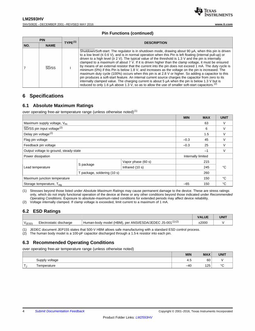
Pin Functions (continued)PIN
TYPE (1) DESCRIPTIONNO. NAME
7 SD/SS I
Shutdown/Soft-start: The regulator is in shutdown mode, drawing about 90 μA, when this pin is drivento a low level (≤ 0.6 V), and is in normal operation when this Pin is left floating (internal pull-up) ordriven to a high level (≥ 2 V). The typical value of the threshold is 1.3 V and the pin is internallyclamped to a maximum of about 7 V. If it is driven higher than the clamp voltage, it must be ensuredby means of an external resistor that the current into the pin does not exceed 1 mA. The duty cycle isminimum (0%) if this Pin is below 1.8 V, and increases as the voltage on the pin is increased. Themaximum duty cycle (100%) occurs when this pin is at 2.8 V or higher. So adding a capacitor to thispin produces a soft-start feature. An internal current source charges the capacitor from zero to itsinternally clamped value. The charging current is about 5 μA when the pin is below 1.3 V but isreduced to only 1.6 μA above 1.3 V, so as to allow the use of smaller soft-start capacitors. (2)
(1) Stresses beyond those listed under Absolute Maximum Ratings may cause permanent damage to the device. These are stress ratingsonly, which do not imply functional operation of the device at these or any other conditions beyond those indicated under RecommendedOperating Conditions. Exposure to absolute-maximum-rated conditions for extended periods may affect device reliability.
(2) Voltage internally clamped. If clamp voltage is exceeded, limit current to a maximum of 1 mA.
6 Specifications
6.1 Absolute Maximum Ratingsover operating free-air temperature range (unless otherwise noted) (1)
MIN MAX UNITMaximum supply voltage, VIN 63 VSD/SS pin input voltage (2) 6 VDelay pin voltage (2) 1.5 VFlag pin voltage –0.3 45 VFeedback pin voltage –0.3 25 VOutput voltage to ground, steady-state –1 VPower dissipation Internally limited
Lead temperatureS package
Vapor phase (60 s) 215°CInfrared (10 s) 245
T package, soldering (10 s) 260Maximum junction temperature 150 °CStorage temperature, Tstg –65 150 °C
(1) JEDEC document JEP155 states that 500-V HBM allows safe manufacturing with a standard ESD control process.(2) The human body model is a 100-pF capacitor discharged through a 1.5-k resistor into each pin.
6.2 ESD RatingsVALUE UNIT
V(ESD) Electrostatic discharge Human-body model (HBM), per ANSI/ESDA/JEDEC JS-001 (1) (2) ±2000 V
6.3 Recommended Operating Conditionsover operating free-air temperature range (unless otherwise noted)
MIN MAX UNITSupply voltage 4.5 60 V
TJ Temperature –40 125 °C

5
LM2593HVwww.ti.com SNVS082E –DECEMBER 2001–REVISED MAY 2016
Product Folder Links: LM2593HV
Submit Documentation FeedbackCopyright © 2001–2016, Texas Instruments Incorporated
(1) For more information about traditional and new thermal metrics, see the Semiconductor and IC Package Thermal Metrics applicationreport, SPRA953.
(2) Junction to ambient thermal resistance (no external heat sink) for the package mounted TO-220 package mounted vertically, with theleads soldered to a printed-circuit board with (1 oz) copper area of approximately 1 in2.
(3) Junction to ambient thermal resistance with the TO-263 package tab soldered to a single-sided printed-circuit board with 0.5 in2 of (1 oz)copper area.
(4) Junction to ambient thermal resistance with the TO-263 package tab soldered to a single-sided printed-circuit board with 2.5 in2 of (1 oz)copper area.
(5) Junction to ambient thermal resistance with the TO-263 package tab soldered to a double-sided printed-circuit board with 3 in2 of (1 oz)copper area on the LM2593HVS side of the board, and approximately 16 in2 of copper on the other side of the printed-circuit board.
6.4 Thermal Information
THERMAL METRIC (1)LM2593HV
UNITNDZ (TO-220) KTW (TO-263)7 PINS 7 PINS
RθJA Junction-to-ambient thermal resistance 50 (2)
50 (3)
°C/W30 (4)
20 (5)
RθJC(top) Junction-to-case (top) thermal resistance 2 2 °C/WRθJB Junction-to-board thermal resistance — — °C/WψJT Junction-to-top characterization parameter — — °C/WψJB Junction-to-board characterization parameter — — °C/WRθJC(bot) Junction-to-case (bottom) thermal resistance — — °C/W
(1) All limits specified at room temperature unless otherwise noted. All room temperature limits are 100% production tested. All limits attemperature extremes are ensured via correlation using standard Statistical Quality Control (SQC) methods. All limits are used tocalculate Average Outgoing Quality Level (AOQL).
(2) Typical numbers are at 25°C and represent the most likely norm.(3) The switching frequency is reduced when the second stage current limit is activated. The amount of reduction is determined by the
severity of current overload.(4) No diode, inductor or capacitor connected to output pin.(5) Feedback pin removed from output and connected to 0 V to force the output transistor switch ON.
6.5 Electrical CharacteristicsTJ = 25°C, VIN = 12 V for the 3.3-V, 5-V, and adjustable versions, and ILOAD = 500 mA (unless otherwise noted)
PARAMETER TEST CONDITIONS MIN (1) TYP (2) MAX (1) UNIT
Ib Feedback bias current Adjustable version only, VFB = 1.3 V 50 10 100 nA
fO Oscillator frequency (3) TJ = 25°C 127 150 173kHz
TJ = –40°C to 125°C 110 173
VSAT Saturation voltage
IOUT = 2 A; no diode, inductoror capacitor connected tooutput pin (4); Feedback pinremoved from output andconnected to 0 V to force theoutput transistor switch ON (5)
TJ = 25°C 1.1 1.3
VTJ = –40°C to 125°C 1.4
DC
Max duty cycle (ON) Feedback pin removed from output and connected to 0V to force the output transistor switch ON 100%
Min duty cycle (OFF)Feedback pin removed from output and connected to12 V for the 3.3-V, 5-V, and the adjustable versions toforce the output transistor switch OFF
0%
ICLIM Switch current limit
Peak current; no diode,inductor or capacitor connectedto output pin; Feedback pinremoved from output andconnected to 0 V to force theoutput transistor switch ON
TJ = 25°C 2.4 3 3.7
ATJ = –40°C to 125°C 2.3 4
IL Output leakage current
Feedback pin removed from output and connected to12 V for the 3.3-V, 5-V, and the adjustable version toforce the output transistor switch OFF; VIN = 60 V,output = 0 V,output = −1 V
50 5 30 mA
IQ Operating quiescent current
SD and SS pin open, Feedback pin removed fromoutput and connected to 12 V for the 3.3-V, 5-V, andthe adjustable version to force the output transistorswitch OFF
5 10 mA
6
LM2593HVSNVS082E –DECEMBER 2001–REVISED MAY 2016 www.ti.com
Product Folder Links: LM2593HV
Submit Documentation Feedback Copyright © 2001–2016, Texas Instruments Incorporated
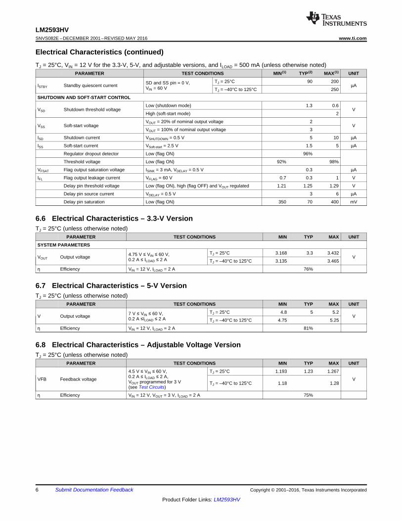
Electrical Characteristics (continued)TJ = 25°C, VIN = 12 V for the 3.3-V, 5-V, and adjustable versions, and ILOAD = 500 mA (unless otherwise noted)
PARAMETER TEST CONDITIONS MIN (1) TYP (2) MAX (1) UNIT
ISTBY Standby quiescent current SD and SS pin = 0 V,VIN = 60 V
TJ = 25°C 90 200µA
TJ = –40°C to 125°C 250
SHUTDOWN AND SOFT-START CONTROL
VSD Shutdown threshold voltageLow (shutdown mode) 1.3 0.6
VHigh (soft-start mode) 2
VSS Soft-start voltageVOUT = 20% of nominal output voltage 2
VVOUT = 100% of nominal output voltage 3
ISD Shutdown current VSHUTDOWN = 0.5 V 5 10 µA
ISS Soft-start current VSoft-start = 2.5 V 1.5 5 µA
Regulator dropout detector Low (flag ON) 96%
Threshold voltage Low (flag ON) 92% 98%
VFSAT Flag output saturation voltage ISINK = 3 mA, VDELAY = 0.5 V 0.3 µA
IFL Flag output leakage current VFLAG = 60 V 0.7 0.3 1 V
Delay pin threshold voltage Low (flag ON), high (flag OFF) and VOUT regulated 1.21 1.25 1.29 V
Delay pin source current VDELAY = 0.5 V 3 6 µA
Delay pin saturation Low (flag ON) 350 70 400 mV
6.6 Electrical Characteristics – 3.3-V VersionTJ = 25°C (unless otherwise noted)
PARAMETER TEST CONDITIONS MIN TYP MAX UNIT
SYSTEM PARAMETERS
VOUT Output voltage 4.75 V ≤ VIN ≤ 60 V,0.2 A ≤ ILOAD ≤ 2 A
TJ = 25°C 3.168 3.3 3.432V
TJ = –40°C to 125°C 3.135 3.465
η Efficiency VIN = 12 V, ILOAD = 2 A 76%
6.7 Electrical Characteristics – 5-V VersionTJ = 25°C (unless otherwise noted)
PARAMETER TEST CONDITIONS MIN TYP MAX UNIT
V Output voltage 7 V ≤ VIN ≤ 60 V,0.2 A ≤ILOAD ≤ 2 A
TJ = 25°C 4.8 5 5.2V
TJ = –40°C to 125°C 4.75 5.25
η Efficiency VIN = 12 V, ILOAD = 2 A 81%
6.8 Electrical Characteristics – Adjustable Voltage VersionTJ = 25°C (unless otherwise noted)
PARAMETER TEST CONDITIONS MIN TYP MAX UNIT
VFB Feedback voltage
4.5 V ≤ VIN ≤ 60 V,0.2 A ≤ ILOAD ≤ 2 A,VOUT programmed for 3 V(see Test Circuits)
TJ = 25°C 1.193 1.23 1.267
VTJ = –40°C to 125°C 1.18 1.28
η Efficiency VIN = 12 V, VOUT = 3 V, ILOAD = 2 A 75%

7
LM2593HVwww.ti.com SNVS082E –DECEMBER 2001–REVISED MAY 2016
Product Folder Links: LM2593HV
Submit Documentation FeedbackCopyright © 2001–2016, Texas Instruments Incorporated
6.9 Typical Characteristics
Figure 1. Normalized Output Voltage Figure 2. Line Regulation
Figure 3. Efficiency Figure 4. Switch Saturation Voltage
Figure 5. Switch Current Limit Figure 6. Dropout Voltage
8
LM2593HVSNVS082E –DECEMBER 2001–REVISED MAY 2016 www.ti.com
Product Folder Links: LM2593HV
Submit Documentation Feedback Copyright © 2001–2016, Texas Instruments Incorporated
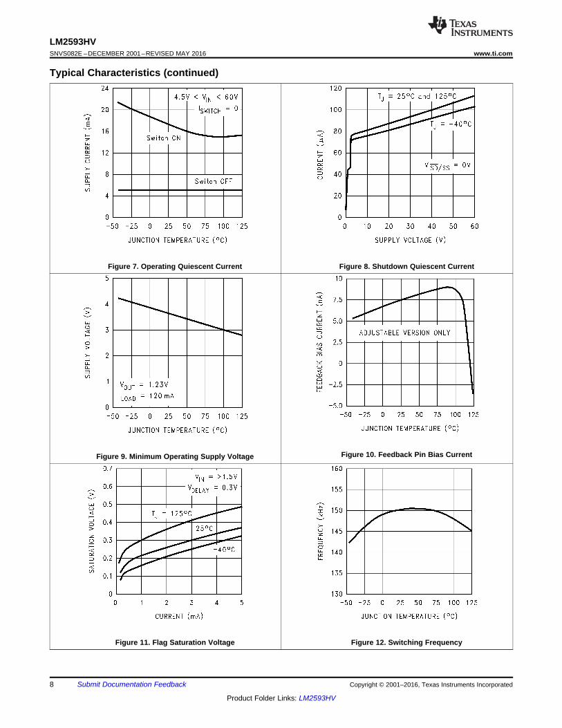
Typical Characteristics (continued)
Figure 7. Operating Quiescent Current Figure 8. Shutdown Quiescent Current
Figure 9. Minimum Operating Supply Voltage Figure 10. Feedback Pin Bias Current
Figure 11. Flag Saturation Voltage Figure 12. Switching Frequency

9
LM2593HVwww.ti.com SNVS082E –DECEMBER 2001–REVISED MAY 2016
Product Folder Links: LM2593HV
Submit Documentation FeedbackCopyright © 2001–2016, Texas Instruments Incorporated
Typical Characteristics (continued)
Figure 13. Soft-Start Figure 14. Shutdown/Soft-Start Current
Figure 15. Delay Pin Current Figure 16. Soft-Start Response
Figure 17. Shutdown/Soft-Start Threshold Voltage Figure 18. Internal Gain-Phase Characteristics

10
LM2593HVSNVS082E –DECEMBER 2001–REVISED MAY 2016 www.ti.com
Product Folder Links: LM2593HV
Submit Documentation Feedback Copyright © 2001–2016, Texas Instruments Incorporated
Typical Characteristics (continued)
Horizontal Time Base: 2 µs/div.VIN = 20 V, VOUT = 5 V, ILOAD = 2 A,L = 32 µH, COUT = 220 µF, COUT ESR = 50 mΩOutput Pin Voltage, 10 V/div.Inductor Current, 1 A/div.Output Ripple Voltage, 50 mV/div.
Figure 19. Continuous Mode Switching Waveforms
Horizontal Time Base: 2 µs/div.VIN = 20 V, VOUT = 5 V, ILOAD = 500 mA,L = 10 µH, COUT = 330 µF, COUT ESR = 50 mΩOutput Pin Voltage, 10 V/div.Inductor Current, 0.5 A/div.Output Ripple Voltage, 100 mV/div.
Figure 20. Discontinuous Mode Switching Waveforms
Horizontal Time Base: 50 µs/div.VIN = 20 V, VOUT = 5 V, ILOAD = 500 mA to 2 A,L = 32 µH, COUT = 220 µF, COUT ESR = 50 mΩOutput Voltage, 100 mV/div. (AC)500-mA to 2-A Load Pulse
Figure 21. Load Transient Responsefor Continuous Mode
Horizontal Time Base: 200 µs/div.VIN = 20 V, VOUT = 5 V, ILOAD = 500 mA to 2 A,L = 10 µH, COUT = 330 µF, COUT ESR = 50 mΩOutput Voltage, 100 mV/div. (AC)500-mA to 2-A Load Pulse
Figure 22. Load Transient Responsefor Discontinuous Mode
11
LM2593HVwww.ti.com SNVS082E –DECEMBER 2001–REVISED MAY 2016
Product Folder Links: LM2593HV
Submit Documentation FeedbackCopyright © 2001–2016, Texas Instruments Incorporated
7 Parameter Measurement Information
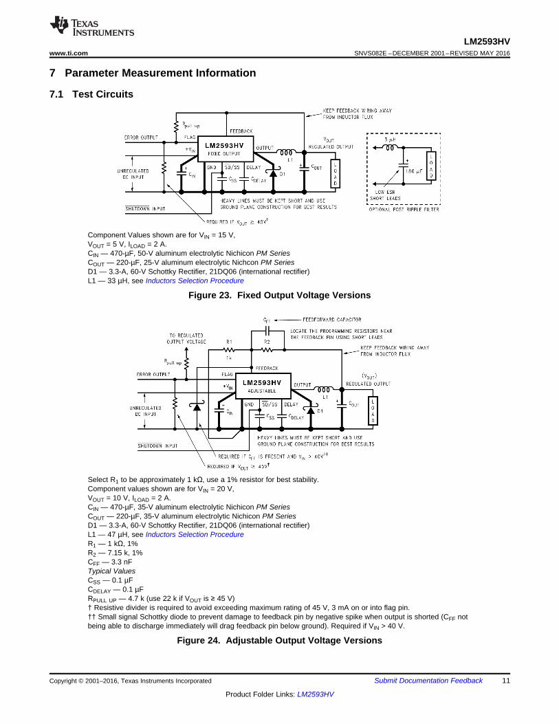
7.1 Test Circuits
Component Values shown are for VIN = 15 V,VOUT = 5 V, ILOAD = 2 A.CIN — 470-µF, 50-V aluminum electrolytic Nichicon PM SeriesCOUT — 220-µF, 25-V aluminum electrolytic Nichcon PM SeriesD1 — 3.3-A, 60-V Schottky Rectifier, 21DQ06 (international rectifier)L1 — 33 µH, see Inductors Selection Procedure
Figure 23. Fixed Output Voltage Versions
Select R1 to be approximately 1 kΩ, use a 1% resistor for best stability.Component values shown are for VIN = 20 V,VOUT = 10 V, ILOAD = 2 A.CIN — 470-µF, 35-V aluminum electrolytic Nichicon PM SeriesCOUT — 220-µF, 35-V aluminum electrolytic Nichicon PM SeriesD1 — 3.3-A, 60-V Schottky Rectifier, 21DQ06 (international rectifier)L1 — 47 µH, see Inductors Selection ProcedureR1 — 1 kΩ, 1%R2 — 7.15 k, 1%CFF — 3.3 nFTypical ValuesCSS — 0.1 µFCDELAY — 0.1 µFRPULL UP — 4.7 k (use 22 k if VOUT is ≥ 45 V)† Resistive divider is required to avoid exceeding maximum rating of 45 V, 3 mA on or into flag pin.†† Small signal Schottky diode to prevent damage to feedback pin by negative spike when output is shorted (CFF notbeing able to discharge immediately will drag feedback pin below ground). Required if VIN > 40 V.
Figure 24. Adjustable Output Voltage Versions

Copyright © 2016, Texas Instruments Incorporated
12
LM2593HVSNVS082E –DECEMBER 2001–REVISED MAY 2016 www.ti.com
Product Folder Links: LM2593HV
Submit Documentation Feedback Copyright © 2001–2016, Texas Instruments Incorporated
8 Detailed Description
8.1 OverviewThe LM2593HV SIMPLE SWITCHER® regulator is an easy-to-use, non-synchronous, step-down DC-DCconverter with a wide input voltage range up to 60 V. It is capable of delivering up to 2-A DC load current withexcellent line and load regulation. These devices are available in fixed output voltages of 3.3-V, 5-V, and anadjustable output version. The family requires few external components and the pin arrangement was designedfor simple, optimum PCB layout.
8.2 Functional Block Diagram
8.3 Feature Description
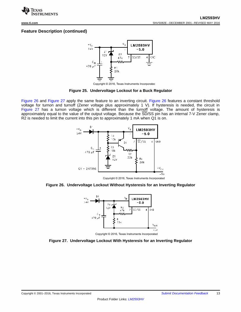
8.3.1 Undervoltage LockoutSome applications require the regulator to remain off until the input voltage reaches a predetermined voltage.Figure 25 contains a undervoltage lockout circuit for a buck configuration, while Figure 26 and Figure 27 are forthe inverting types (only the circuitry pertaining to the undervoltage lockout is shown). Figure 25 uses a Zenerdiode to establish the threshold voltage when the switcher begins operating. When the input voltage is less thanthe Zener voltage, resistors R1 and R2 hold the Shutdown/Soft-Start pin low, keeping the regulator in theshutdown mode. As the input voltage exceeds the Zener voltage, the Zener conducts, pulling the Shutdown/Soft-Start pin high, allowing the regulator to begin switching. The threshold voltage for the undervoltage lockoutfeature is approximately 1.5 V greater than the Zener voltage.
Copyright © 2016, Texas Instruments Incorporated
Copyright © 2016, Texas Instruments Incorporated
Copyright © 2016, Texas Instruments Incorporated
13
LM2593HVwww.ti.com SNVS082E –DECEMBER 2001–REVISED MAY 2016
Product Folder Links: LM2593HV
Submit Documentation FeedbackCopyright © 2001–2016, Texas Instruments Incorporated
Feature Description (continued)
Figure 25. Undervoltage Lockout for a Buck Regulator
Figure 26 and Figure 27 apply the same feature to an inverting circuit. Figure 26 features a constant thresholdvoltage for turnon and turnoff (Zener voltage plus approximately 1 V). If hysteresis is needed, the circuit inFigure 27 has a turnon voltage which is different than the turnoff voltage. The amount of hysteresis isapproximately equal to the value of the output voltage. Because the SD/SS pin has an internal 7-V Zener clamp,R2 is needed to limit the current into this pin to approximately 1 mA when Q1 is on.
Figure 26. Undervoltage Lockout Without Hysteresis for an Inverting Regulator
Figure 27. Undervoltage Lockout With Hysteresis for an Inverting Regulator

Copyright © 2016, Texas Instruments Incorporated
14
LM2593HVSNVS082E –DECEMBER 2001–REVISED MAY 2016 www.ti.com
Product Folder Links: LM2593HV
Submit Documentation Feedback Copyright © 2001–2016, Texas Instruments Incorporated
Feature Description (continued)8.3.2 Negative Voltage Charge PumpOccasionally a low current negative voltage is needed for biasing parts of a circuit. A simple method ofgenerating a negative voltage using a charge pump technique is shown in Figure 28. This unregulated negativevoltage is approximately equal to the positive input voltage (minus a few volts), and can supply up to a 600 mA ofoutput current. There is a requirement however, that there be a minimum load of 1.2 A on the regulated positiveoutput for the charge pump to work correctly. Also, resistor R1 is required to limit the charging current of C1 tosome value less than the LM2593HV current limit. This method of generating a negative output voltage withoutan additional inductor can be used with other members of the SIMPLE SWITCHER® family, using either the buckor boost topology.
Figure 28. Charge Pump for Generating a Low-Current, Negative Output Voltage
8.3.3 Shutdown/Soft-StartThis reduction in start-up current is useful in situations where the input power source is limited in the amount ofcurrent it can deliver. In some applications, soft-start can be used to replace undervoltage lockout or delayedstart-up functions. If a very slow output voltage ramp is desired, the soft-start capacitor can be made muchlarger. Many seconds or even minutes are possible. If only the shutdown feature is needed, the soft-startcapacitor can be eliminated.
Figure 29. Typical Circuit Using Shutdown/Soft-Start and Error Flag Features

10133331
15
LM2593HVwww.ti.com SNVS082E –DECEMBER 2001–REVISED MAY 2016
Product Folder Links: LM2593HV
Submit Documentation FeedbackCopyright © 2001–2016, Texas Instruments Incorporated
Feature Description (continued)
Figure 30. Soft-Start, Delay, Error Output
8.4 Device Functional Modes
8.4.1 Shutdown ModeThe Shutdown/Soft-start pin provides electrical ON and OFF control for the LM2593HV. When the voltage of thispin is less than 0.6 V, the device is in shutdown mode. The typical standby current in this mode is 90 μA.
8.4.2 Active ModeWhen the Shutdown/Soft-start pin is left floating or pull above 2 V, the device starts switching and the outputvoltage rises until it reaches a normal regulation voltage.
16
LM2593HVSNVS082E –DECEMBER 2001–REVISED MAY 2016 www.ti.com
Product Folder Links: LM2593HV
Submit Documentation Feedback Copyright © 2001–2016, Texas Instruments Incorporated
9 Application and Implementation
NOTEInformation in the following applications sections is not part of the TI componentspecification, and TI does not warrant its accuracy or completeness. TI’s customers areresponsible for determining suitability of components for their purposes. Customers shouldvalidate and test their design implementation to confirm system functionality.
9.1 Application Information
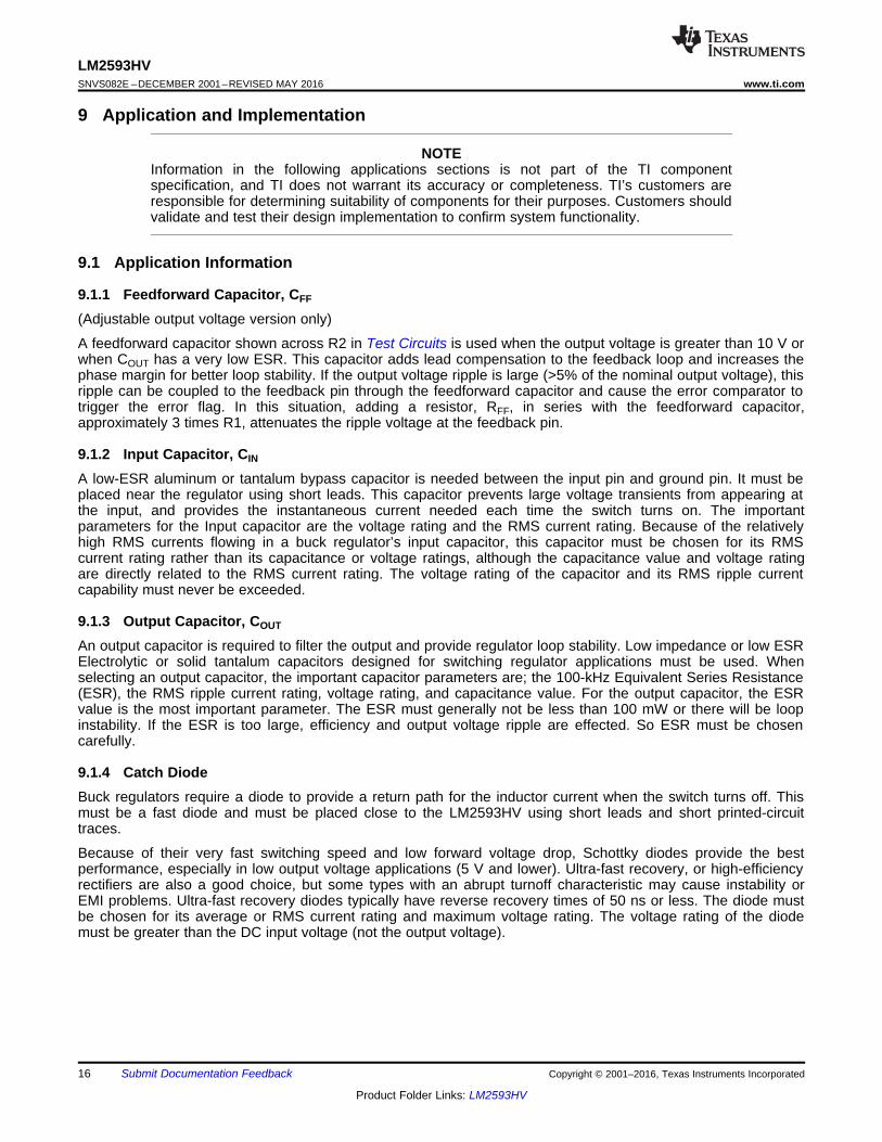
9.1.1 Feedforward Capacitor, CFF
(Adjustable output voltage version only)
A feedforward capacitor shown across R2 in Test Circuits is used when the output voltage is greater than 10 V orwhen COUT has a very low ESR. This capacitor adds lead compensation to the feedback loop and increases thephase margin for better loop stability. If the output voltage ripple is large (>5% of the nominal output voltage), thisripple can be coupled to the feedback pin through the feedforward capacitor and cause the error comparator totrigger the error flag. In this situation, adding a resistor, RFF, in series with the feedforward capacitor,approximately 3 times R1, attenuates the ripple voltage at the feedback pin.
9.1.2 Input Capacitor, CIN
A low-ESR aluminum or tantalum bypass capacitor is needed between the input pin and ground pin. It must beplaced near the regulator using short leads. This capacitor prevents large voltage transients from appearing atthe input, and provides the instantaneous current needed each time the switch turns on. The importantparameters for the Input capacitor are the voltage rating and the RMS current rating. Because of the relativelyhigh RMS currents flowing in a buck regulator’s input capacitor, this capacitor must be chosen for its RMScurrent rating rather than its capacitance or voltage ratings, although the capacitance value and voltage ratingare directly related to the RMS current rating. The voltage rating of the capacitor and its RMS ripple currentcapability must never be exceeded.
9.1.3 Output Capacitor, COUT
An output capacitor is required to filter the output and provide regulator loop stability. Low impedance or low ESRElectrolytic or solid tantalum capacitors designed for switching regulator applications must be used. Whenselecting an output capacitor, the important capacitor parameters are; the 100-kHz Equivalent Series Resistance(ESR), the RMS ripple current rating, voltage rating, and capacitance value. For the output capacitor, the ESRvalue is the most important parameter. The ESR must generally not be less than 100 mW or there will be loopinstability. If the ESR is too large, efficiency and output voltage ripple are effected. So ESR must be chosencarefully.
9.1.4 Catch DiodeBuck regulators require a diode to provide a return path for the inductor current when the switch turns off. Thismust be a fast diode and must be placed close to the LM2593HV using short leads and short printed-circuittraces.
Because of their very fast switching speed and low forward voltage drop, Schottky diodes provide the bestperformance, especially in low output voltage applications (5 V and lower). Ultra-fast recovery, or high-efficiencyrectifiers are also a good choice, but some types with an abrupt turnoff characteristic may cause instability orEMI problems. Ultra-fast recovery diodes typically have reverse recovery times of 50 ns or less. The diode mustbe chosen for its average or RMS current rating and maximum voltage rating. The voltage rating of the diodemust be greater than the DC input voltage (not the output voltage).
( )
6
IN OUT IN OUTPEAK LOAD
IN IN OUT
V V V V 10I I
V 2 L f V V
æ ö+ ´ ´= ´ +ç ÷
´ ´ ´ +è ø
17
LM2593HVwww.ti.com SNVS082E –DECEMBER 2001–REVISED MAY 2016
Product Folder Links: LM2593HV
Submit Documentation FeedbackCopyright © 2001–2016, Texas Instruments Incorporated
Application Information (continued)9.1.5 lnverting RegulatorThe circuit in Figure 31 converts a positive input voltage to a negative output voltage with a common ground. Thecircuit operates by bootstrapping the regulator’s ground pin to the negative output voltage, then grounding thefeedback pin, the regulator senses the inverted output voltage and regulates it. This example uses theLM2593HV 5-V to generate a −5-V output, but other output voltages are possible by selecting other outputvoltage versions, including the adjustable version. Because this regulator topology can produce an output voltagethat is either greater than or less than the input voltage, the maximum output current greatly depends on both theinput and output voltage. To determine how much load current is possible before the internal device current limitis reached (and power limiting occurs), the system must be evaluated as a buck-boost configuration rather thanas a buck. The peak switch current in amperes, for such a configuration is given as Equation 1.
where• L is in μH• f is in Hz (1)
The maximum possible load current ILOAD is limited by the requirement that IPEAK ≤ ICLIM. While checking for this,take ICLIM to be the lowest possible current limit value (minimum across tolerance and temperature is 2.3 A forthe LM2593HV). Also to account for inductor tolerances, take the minimum value of Inductance for L inEquation 1 (typically 20% less than the nominal value). Further, the above equation disregards the drop acrossthe switch and the diode. This is equivalent to assuming 100% efficiency, which is never so. Therefore expectIPEAK to be an additional 10-20% higher than calculated from Equation 1. See also Application Note AN-1197Selecting Inductors for Buck Converters (SNVA038) for examples based on positive to negative configuration.The maximum voltage appearing across the regulator is the absolute sum of the input and output voltage. Thismust be limited to a maximum of 60 V. In this example, when converting 20 V to −5 V, the regulator would see25 V between the input pin and ground pin. The LM2593HV has a maximum input voltage rating of 60 V. Anadditional diode is required in this regulator configuration. Diode D1 is used to isolate input voltage ripple ornoise from coupling through the CIN capacitor to the output, under light or no load conditions. Also, this diodeisolation changes the topology to closely resemble a buck configuration thus providing good closed-loop stability.A Schottky diode is recommended for low input voltages, (because of its lower voltage drop) but for higher inputvoltages, a IN5400 diode could be used. Because of differences in the operation of the inverting regulator, thestandard design procedure is not used to select the inductor value. In the majority of designs, a 33-μH, 4-Ainductor is the best choice. Capacitor selection can also be narrowed down to just a few values. This type ofinverting regulator can require relatively large amounts of input current when starting up, even with light loads.Input currents as high as the LM2593HV current limit (approximately 4 A) are needed for 2 ms or more, until theoutput reaches its nominal output voltage. The actual time depends on the output voltage and the size of theoutput capacitor. Input power sources that are current limited or sources that can not deliver these currentswithout getting loaded down, may not work correctly. Because of the relatively high start-up currents required bythe inverting topology, the soft-start feature shown in Figure 31 is recommended. Also shown in Figure 31 areseveral shutdown methods for the inverting configuration. With the inverting configuration, some level shifting isrequired, because the ground pin of the regulator is no longer at ground, but is now at the negative outputvoltage. The shutdown methods shown accept ground referenced shutdown signals.

Copyright © 2016, Texas Instruments Incorporated
18
LM2593HVSNVS082E –DECEMBER 2001–REVISED MAY 2016 www.ti.com
Product Folder Links: LM2593HV
Submit Documentation Feedback Copyright © 2001–2016, Texas Instruments Incorporated
Application Information (continued)
Figure 31. Inverting −5 V Regulator With Shutdown and Soft-Start
9.2 Typical Application
Figure 32. LM2593HV 5-V Application Schematic
9.2.1 Design RequirementsTable 1 lists the example values for this typical application.
Table 1. Application Example ParametersDESIGN PARAMETER EXAMPLE VALUE
Regulated output voltage (3.3 V, 5 V, or adjustable), VOUT 5 VMaximum input voltage, VIN(max) 24 VMaximum load current, ILOAD(max) 1 A
Switching frequency, F Fixed at a nominal 150 kHz
2
CLIM
1e L I J
2= ´ ´ m
2
PEAK
1e L I J
2= ´ ´ m
19
LM2593HVwww.ti.com SNVS082E –DECEMBER 2001–REVISED MAY 2016
Product Folder Links: LM2593HV
Submit Documentation FeedbackCopyright © 2001–2016, Texas Instruments Incorporated
9.2.2 Detailed Design Procedure
9.2.2.1 Inductors Selection ProcedureSee application note AN-1197 Selecting Inductors for Buck Converters (SNVA038) for detailed information oninductor selection. For a quick-start, see the nomographs provided in Figure 33 to Figure 35. To widen thechoices to a more general selection of available inductors, the nomographs provide the required inductance andalso the energy in the core expressed in microjoules (μJ), as an alternative to just prescribing custom parts. Thefollowing points must be highlighted:1. The energy values shown on the nomographs apply to steady operation at the corresponding x-coordinate
(rated maximum load current). However under start-up, without soft-start, or a short-circuit on the output, thecurrent in the inductor momentarily and repetitively hits the current limit ICLIM of the device, and this currentcould be much higher than the rated load, ILOAD. This represents an overload situation, and can cause theinductor to saturate (if it has been designed only to handle the energy of steady operation). However mosttypes of core structures used for such applications have a large inherent air gap (for example powdered irontypes or ferrite rod inductors), and so the inductance does not fall off too sharply under an overload. Thedevice is usually able to protect itself by not allowing the current to ever exceed ICLIM. But if the DC inputvoltage to the regulator is over 40 V, the current can slew up so fast under core saturation, that the devicemay not be able to act fast enough to restrict the current. The current can then rise without limit tilldestruction of the device takes place. Therefore to ensure reliability, TI recommends, that if the DC inputvoltage exceeds 40 V, the inductor must always be sized to handle an instantaneous current equal to ICLIMwithout saturating, irrespective of the type of core structure or material.
2. Use Equation 2 to calculate the energy under steady operation.
where• L is in μH• IPEAK is the peak of the inductor current waveform with the regulator delivering ILOAD (2)
These are the energy values shown in the nomographs. See Example 1.3. The energy under overload is Equation 3.
where• L is in μH• IPEAK is the peak of the inductor current waveform with the regulator delivering ILOAD (3)
If VIN > 40 V, the inductor must be sized to handle eCLIM instead of the steady energy values. The worst caseICLIM for the LM2593HV is 4 A. The energy rating depends on the inductance. See Example 2.
4. The nomographs were generated by allowing a greater amount of percentage current ripple in the inductoras the maximum rated load decreases (see Figure 36). This was done to permit the use of smaller inductorsat light loads. However, Figure 36 shows only the median value of the current ripple. In reality there may bea great spread around this because the nomographs approximate the exact calculated inductance tostandard available values. It is a good idea to refer to AN-1197 Selecting Inductors for Buck Converters(SNVA038) for detailed calculations if a certain maximum inductor current ripple is required for variouspossible reasons. Also consider the rather wide tolerance on the nominal inductance of commercialinductors.
5. Figure 35 shows the inductor selection curves for the adjustable version. The y-axis is Et, in Vμs. It is theapplied volts across the inductor during the ON time of the switch (VIN-VSAT-VOUT) multiplied by the time forwhich the switch is on in μs. See Example 3.
9.2.2.1.1 Example 1: VIN ≤ 40 V, 5-V Version, VIN = 24 V, Output = 5 V at 1 A1. A first pass inductor selection is based upon inductance and rated maximum load current. Choose an
inductor with the inductance value indicated by the nomograph (see Figure 34) and a current rating equal tothe maximum load current. Therefore, quick-select a 68-μH, 1-A inductor (designed for 150-kHz operation)for this application.
( )
( )
IN SAT OUT ON
6
Et V V V t
0.5520 1.5 10 10 V sec s
150000
31.3 V sec s
= - - ´
= - - ´ ´ m
= m
6
ON
Dt 10 s
f= ´ m
10 0.5D 0.55
20 1.5 0.5
+= =
- +
OUT D
IN SAT D
V VD
V V V
+
=
- +
2
CLIM
1e 68 4 544 J
2= ´ ´ = m
20
LM2593HVSNVS082E –DECEMBER 2001–REVISED MAY 2016 www.ti.com
Product Folder Links: LM2593HV
Submit Documentation Feedback Copyright © 2001–2016, Texas Instruments Incorporated
2. Confirm that it is rated to handle 50 μJ (see Figure 34) by either estimating the peak current or by a detailedcalculation as shown in AN-1197 Selecting Inductors for Buck Converters (SNVA038), and also that thelosses are acceptable.
9.2.2.1.2 Example 2: VIN > 40 V, 5-V version, VIN = 48 V, Output = 5 V at 1.5 A1. A first pass inductor selection is based upon inductance and the switch currrent limit. Choose an inductor
with the inductance value indicated by the nomograph (see Figure 34) and a current rating equal to ICLIM.Therefore, quick-select a 68-μH, 4-A inductor (designed for 150-kHz operation) for this application.
2. Confirm that it is rated to handle eCLIM by the procedure shown in AN-1197 Selecting Inductors for BuckConverters (SNVA038) and that the losses are acceptable. Here eCLIM is Equation 4.
(4)
9.2.2.1.3 Example 3: VIN ≤ 40 V, Adjustable Version, VIN = 20 V, Output = 10 V at 2 A1. Because input voltage is less than 40 V, a first pass inductor selection is based upon inductance and rated
maximum load current. Choose an inductor with the inductance value indicated by the nomograph Figure 35and a current rating equal to the maximum load. But first calculate Et for the given application. The dutycycle is Equation 5.
where• VD is the drop across the catch diode (0.5 V for a Schottky)• VSAT the drop across the switch (1.5 V) (5)
So this yields Equation 6.
(6)2. The switch ON time is calculated with Equation 7.
where• f is the switching frequency in Hz (7)
So this yields Equation 8.
(8)3. Therefore, looking at Figure 33, quick-select a 47-μH, 2-A inductor (designed for 150-kHz operation) for this
application.4. Confirm that it is rated to handle 200 μJ (see Figure 35) by the procedure shown in AN-1197 Selecting
Inductors for Buck Converters (SNVA038) and that the losses are acceptable. (If the DC input voltage hadbeen greater than 40 V, consider eCLIM as in Example 2).
This completes the simplified inductor selection procedure. For more general applications and betteroptimization, refer to AN-1197 Selecting Inductors for Buck Converters (SNVA038).

21
LM2593HVwww.ti.com SNVS082E –DECEMBER 2001–REVISED MAY 2016
Product Folder Links: LM2593HV
Submit Documentation FeedbackCopyright © 2001–2016, Texas Instruments Incorporated
9.2.3 Application CurvesFor continuous mode operation
Figure 33. LM2593HV 3.3-V Figure 34. LM2593HV 5-V
Figure 35. LM2593HV Adjustable Voltage Figure 36. Current Ripple Ratio
22
LM2593HVSNVS082E –DECEMBER 2001–REVISED MAY 2016 www.ti.com
Product Folder Links: LM2593HV
Submit Documentation Feedback Copyright © 2001–2016, Texas Instruments Incorporated
10 Power Supply RecommendationsThe LM2593HV is designed to operate from an input voltage supply up to 60 V. This input supply must be wellregulated and able to withstand maximum input current and maintain a stable voltage.
11 Layout
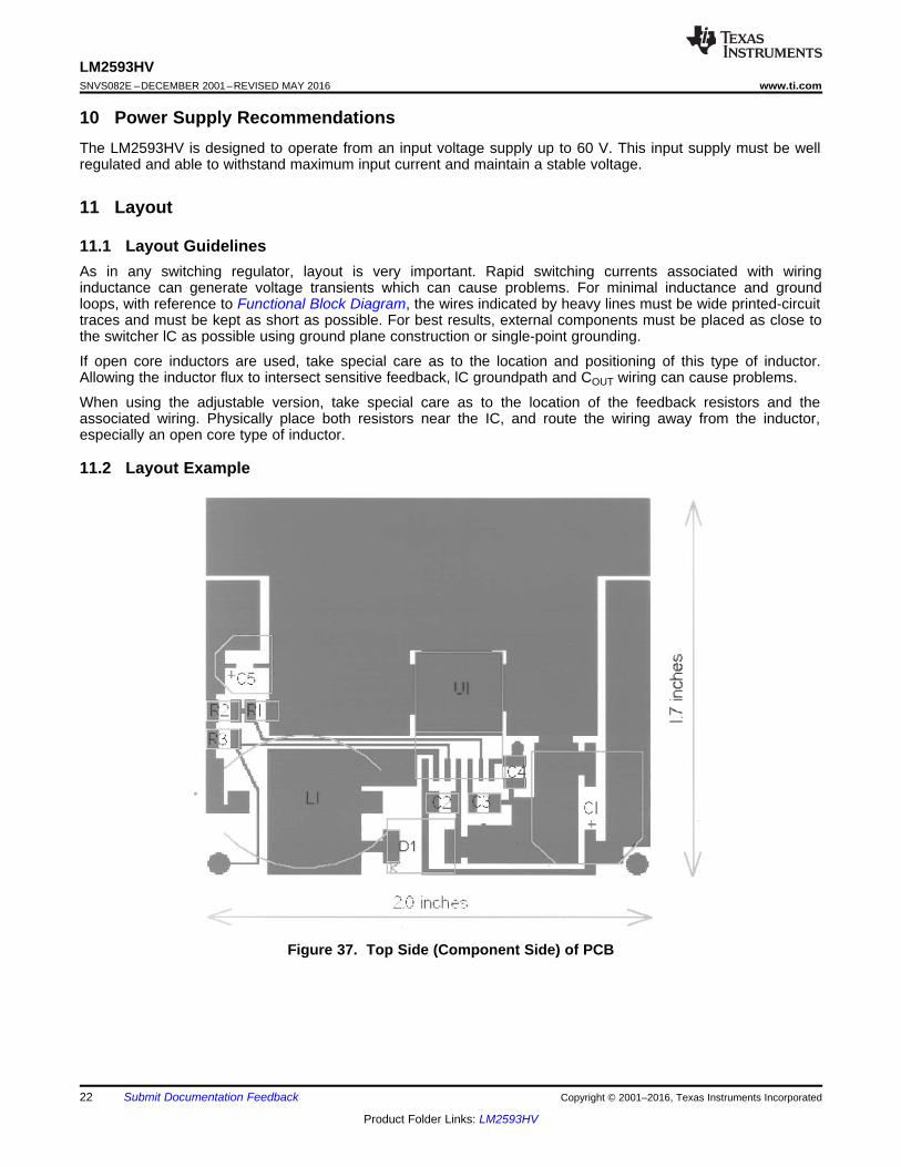
11.1 Layout GuidelinesAs in any switching regulator, layout is very important. Rapid switching currents associated with wiringinductance can generate voltage transients which can cause problems. For minimal inductance and groundloops, with reference to Functional Block Diagram, the wires indicated by heavy lines must be wide printed-circuittraces and must be kept as short as possible. For best results, external components must be placed as close tothe switcher lC as possible using ground plane construction or single-point grounding.
If open core inductors are used, take special care as to the location and positioning of this type of inductor.Allowing the inductor flux to intersect sensitive feedback, lC groundpath and COUT wiring can cause problems.
When using the adjustable version, take special care as to the location of the feedback resistors and theassociated wiring. Physically place both resistors near the IC, and route the wiring away from the inductor,especially an open core type of inductor.
11.2 Layout Example
Figure 37. Top Side (Component Side) of PCB

23
LM2593HVwww.ti.com SNVS082E –DECEMBER 2001–REVISED MAY 2016
Product Folder Links: LM2593HV
Submit Documentation FeedbackCopyright © 2001–2016, Texas Instruments Incorporated
11.3 Thermal ConsiderationsThe LM2593HV is available in two packages, a 5-pin TO-220 (T) and a 5-pin surface-mount TO-263 (S). TheTO-220 package needs a heat sink under most conditions. The size of the heat sink depends on the inputvoltage, the output voltage, the load current, and the ambient temperature. Higher ambient temperatures requiremore heat sinking. The TO-263 surface-mount package tab is designed to be soldered to the copper on aprinted-circuit board. The copper and the board are the heat sink for this package and the other heat-producingcomponents, such as the catch diode and inductor. The PCB copper area that the package is soldered to mustbe at least 0.4 in2, and ideally must have 2 or more square inches of 2-oz. (0.0028 in) copper. Additional copperarea improves the thermal characteristics, but with copper areas greater than approximately 6 in2, only smallimprovements in heat dissipation are realized. If further thermal improvements are needed, double-sided,multilayer PCB with large copper areas or airflow are recommended. The curves shown in Figure 38 show theLM2593HVS (TO-263 package) junction temperature rise above ambient temperature with a 2-A load for variousinput and output voltages. This data was taken with the circuit operating as a buck switching regulator with allcomponents mounted on a PCB to simulate the junction temperature under actual operating conditions. Thiscurve can be used for a quick check for the approximate junction temperature for various conditions, but beaware that there are many factors that can affect the junction temperature. When load currents higher than 2 Aare used, double-sided or multilayer PCBs with large copper areas or airflow might be required, especially forhigh ambient temperatures and high output voltages. For the best thermal performance, wide copper traces andgenerous amounts of printed-circuit board copper must be used in the board layout. (One exception to this is theoutput (switch) pin, which must not have large areas of copper.) Large areas of copper provide the best transferof heat (lower thermal resistance) to the surrounding air, and moving air lowers the thermal resistance evenfurther. Package thermal resistance and junction temperature rise numbers are all approximate, and there aremany factors that affect these numbers. Some of these factors include board size, shape, thickness, position,location, and even board temperature. Other factors are, trace width, total printed-circuit copper area, copperthickness, single- or double-sided, multilayer board, and the amount of solder on the board. The effectiveness ofthe PCB to dissipate heat also depends on the size, quantity, and spacing of other components on the board, aswell as whether the surrounding air is still or moving. Furthermore, some of these components, such as the catchdiode will add heat to the PCB and the heat can vary as the input voltage changes. For the inductor, dependingon the physical size, type of core material, and the DC resistance, it could either act as a heat sink taking heataway from the board, or it could add heat to the board.
Figure 38. Junction Temperature Rise, TO-263
24
LM2593HVSNVS082E –DECEMBER 2001–REVISED MAY 2016 www.ti.com
Product Folder Links: LM2593HV
Submit Documentation Feedback Copyright © 2001–2016, Texas Instruments Incorporated
12 Device and Documentation Support
12.1 Documentation Support
12.1.1 Related DocumentationFor related documentation see the following:
AN-1197 Selecting Inductors for Buck Converters, SNVA038
12.2 Community ResourcesThe following links connect to TI community resources. Linked contents are provided "AS IS" by the respectivecontributors. They do not constitute TI specifications and do not necessarily reflect TI's views; see TI's Terms ofUse.
TI E2E™ Online Community TI's Engineer-to-Engineer (E2E) Community. Created to foster collaborationamong engineers. At e2e.ti.com, you can ask questions, share knowledge, explore ideas and helpsolve problems with fellow engineers.
Design Support TI's Design Support Quickly find helpful E2E forums along with design support tools andcontact information for technical support.
12.3 TrademarksE2E is a trademark of Texas Instruments.SIMPLE SWITCHER is a registered trademark of Texas Instruments.All other trademarks are the property of their respective owners.
12.4 Electrostatic Discharge CautionThese devices have limited built-in ESD protection. The leads should be shorted together or the device placed in conductive foamduring storage or handling to prevent electrostatic damage to the MOS gates.
12.5 GlossarySLYZ022 — TI Glossary.
This glossary lists and explains terms, acronyms, and definitions.
13 Mechanical, Packaging, and Orderable InformationThe following pages include mechanical, packaging, and orderable information. This information is the mostcurrent data available for the designated devices. This data is subject to change without notice and revision ofthis document. For browser-based versions of this data sheet, refer to the left-hand navigation.

PACKAGE OPTION ADDENDUM
www.ti.com 25-Jan-2016
Addendum-Page 1
PACKAGING INFORMATION
Orderable Device Status(1)
Package Type PackageDrawing
Pins PackageQty
Eco Plan(2)
Lead/Ball Finish(6)
MSL Peak Temp(3)
Op Temp (°C) Device Marking(4/5)
Samples
LM2593HVS-3.3/NOPB ACTIVE DDPAK/TO-263
KTW 7 45 Pb-Free (RoHSExempt)
CU SN Level-3-245C-168 HR -40 to 125 LM2593HVS-3.3 P+
LM2593HVS-5.0/NOPB ACTIVE DDPAK/TO-263
KTW 7 45 Pb-Free (RoHSExempt)
CU SN Level-3-245C-168 HR -40 to 125 LM2593HVS-5.0 P+
LM2593HVS-ADJ NRND DDPAK/TO-263
KTW 7 45 TBD Call TI Call TI -40 to 125 LM2593HVS-ADJ P+
LM2593HVS-ADJ/NOPB ACTIVE DDPAK/TO-263
KTW 7 45 Pb-Free (RoHSExempt)
CU SN Level-3-245C-168 HR -40 to 125 LM2593HVS-ADJ P+
LM2593HVSX-3.3/NOPB ACTIVE DDPAK/TO-263
KTW 7 500 Pb-Free (RoHSExempt)
CU SN Level-3-245C-168 HR -40 to 125 LM2593HVS-3.3 P+
LM2593HVSX-5.0/NOPB ACTIVE DDPAK/TO-263
KTW 7 500 Pb-Free (RoHSExempt)
CU SN Level-3-245C-168 HR -40 to 125 LM2593HVS-5.0 P+
LM2593HVSX-ADJ/NOPB ACTIVE DDPAK/TO-263
KTW 7 500 Pb-Free (RoHSExempt)
CU SN Level-3-245C-168 HR -40 to 125 LM2593HVS-ADJ P+
LM2593HVT-5.0/NOPB ACTIVE TO-220 NDZ 7 45 Green (RoHS& no Sb/Br)
CU SN Level-1-NA-UNLIM -40 to 125 LM2593HVT-5.0 P+
LM2593HVT-ADJ/NOPB ACTIVE TO-220 NDZ 7 45 Green (RoHS& no Sb/Br)
CU SN Level-1-NA-UNLIM -40 to 125 LM2593HVT-ADJ P+
(1) The marketing status values are defined as follows:ACTIVE: Product device recommended for new designs.LIFEBUY: TI has announced that the device will be discontinued, and a lifetime-buy period is in effect.NRND: Not recommended for new designs. Device is in production to support existing customers, but TI does not recommend using this part in a new design.PREVIEW: Device has been announced but is not in production. Samples may or may not be available.OBSOLETE: TI has discontinued the production of the device.
(2) Eco Plan - The planned eco-friendly classification: Pb-Free (RoHS), Pb-Free (RoHS Exempt), or Green (RoHS & no Sb/Br) - please check http://www.ti.com/productcontent for the latest availabilityinformation and additional product content details.TBD: The Pb-Free/Green conversion plan has not been defined.Pb-Free (RoHS): TI's terms "Lead-Free" or "Pb-Free" mean semiconductor products that are compatible with the current RoHS requirements for all 6 substances, including the requirement thatlead not exceed 0.1% by weight in homogeneous materials. Where designed to be soldered at high temperatures, TI Pb-Free products are suitable for use in specified lead-free processes.Pb-Free (RoHS Exempt): This component has a RoHS exemption for either 1) lead-based flip-chip solder bumps used between the die and package, or 2) lead-based die adhesive used betweenthe die and leadframe. The component is otherwise considered Pb-Free (RoHS compatible) as defined above.Green (RoHS & no Sb/Br): TI defines "Green" to mean Pb-Free (RoHS compatible), and free of Bromine (Br) and Antimony (Sb) based flame retardants (Br or Sb do not exceed 0.1% by weightin homogeneous material)

PACKAGE OPTION ADDENDUM
www.ti.com 25-Jan-2016
Addendum-Page 2
(3) MSL, Peak Temp. - The Moisture Sensitivity Level rating according to the JEDEC industry standard classifications, and peak solder temperature.
(4) There may be additional marking, which relates to the logo, the lot trace code information, or the environmental category on the device.
(5) Multiple Device Markings will be inside parentheses. Only one Device Marking contained in parentheses and separated by a "~" will appear on a device. If a line is indented then it is a continuationof the previous line and the two combined represent the entire Device Marking for that device.
(6) Lead/Ball Finish - Orderable Devices may have multiple material finish options. Finish options are separated by a vertical ruled line. Lead/Ball Finish values may wrap to two lines if the finishvalue exceeds the maximum column width.
Important Information and Disclaimer:The information provided on this page represents TI's knowledge and belief as of the date that it is provided. TI bases its knowledge and belief on informationprovided by third parties, and makes no representation or warranty as to the accuracy of such information. Efforts are underway to better integrate information from third parties. TI has taken andcontinues to take reasonable steps to provide representative and accurate information but may not have conducted destructive testing or chemical analysis on incoming materials and chemicals.TI and TI suppliers consider certain information to be proprietary, and thus CAS numbers and other limited information may not be available for release.
In no event shall TI's liability arising out of such information exceed the total purchase price of the TI part(s) at issue in this document sold by TI to Customer on an annual basis.

TAPE AND REEL INFORMATION
*All dimensions are nominal
Device PackageType
PackageDrawing
Pins SPQ ReelDiameter
(mm)
ReelWidth
W1 (mm)
A0(mm)
B0(mm)
K0(mm)
P1(mm)
W(mm)
Pin1Quadrant
LM2593HVSX-3.3/NOPB DDPAK/TO-263
KTW 7 500 330.0 24.4 10.75 14.85 5.0 16.0 24.0 Q2
LM2593HVSX-5.0/NOPB DDPAK/TO-263
KTW 7 500 330.0 24.4 10.75 14.85 5.0 16.0 24.0 Q2
LM2593HVSX-ADJ/NOPB DDPAK/TO-263
KTW 7 500 330.0 24.4 10.75 14.85 5.0 16.0 24.0 Q2
PACKAGE MATERIALS INFORMATION
www.ti.com 25-Jan-2016
Pack Materials-Page 1

*All dimensions are nominal
Device Package Type Package Drawing Pins SPQ Length (mm) Width (mm) Height (mm)
LM2593HVSX-3.3/NOPB DDPAK/TO-263 KTW 7 500 367.0 367.0 45.0
LM2593HVSX-5.0/NOPB DDPAK/TO-263 KTW 7 500 367.0 367.0 45.0
LM2593HVSX-ADJ/NOPB DDPAK/TO-263 KTW 7 500 367.0 367.0 45.0
PACKAGE MATERIALS INFORMATION
www.ti.com 25-Jan-2016
Pack Materials-Page 2

MECHANICAL DATA
NDZ0007B
www.ti.com
TA07B (Rev E)

MECHANICAL DATA
KTW0007B
www.ti.com
BOTTOM SIDE OF PACKAGE
TS7B (Rev E)

IMPORTANT NOTICE
Texas Instruments Incorporated and its subsidiaries (TI) reserve the right to make corrections, enhancements, improvements and otherchanges to its semiconductor products and services per JESD46, latest issue, and to discontinue any product or service per JESD48, latestissue. Buyers should obtain the latest relevant information before placing orders and should verify that such information is current andcomplete. All semiconductor products (also referred to herein as “components”) are sold subject to TI’s terms and conditions of salesupplied at the time of order acknowledgment.TI warrants performance of its components to the specifications applicable at the time of sale, in accordance with the warranty in TI’s termsand conditions of sale of semiconductor products. Testing and other quality control techniques are used to the extent TI deems necessaryto support this warranty. Except where mandated by applicable law, testing of all parameters of each component is not necessarilyperformed.TI assumes no liability for applications assistance or the design of Buyers’ products. Buyers are responsible for their products andapplications using TI components. To minimize the risks associated with Buyers’ products and applications, Buyers should provideadequate design and operating safeguards.TI does not warrant or represent that any license, either express or implied, is granted under any patent right, copyright, mask work right, orother intellectual property right relating to any combination, machine, or process in which TI components or services are used. Informationpublished by TI regarding third-party products or services does not constitute a license to use such products or services or a warranty orendorsement thereof. Use of such information may require a license from a third party under the patents or other intellectual property of thethird party, or a license from TI under the patents or other intellectual property of TI.Reproduction of significant portions of TI information in TI data books or data sheets is permissible only if reproduction is without alterationand is accompanied by all associated warranties, conditions, limitations, and notices. TI is not responsible or liable for such altereddocumentation. Information of third parties may be subject to additional restrictions.Resale of TI components or services with statements different from or beyond the parameters stated by TI for that component or servicevoids all express and any implied warranties for the associated TI component or service and is an unfair and deceptive business practice.TI is not responsible or liable for any such statements.Buyer acknowledges and agrees that it is solely responsible for compliance with all legal, regulatory and safety-related requirementsconcerning its products, and any use of TI components in its applications, notwithstanding any applications-related information or supportthat may be provided by TI. Buyer represents and agrees that it has all the necessary expertise to create and implement safeguards whichanticipate dangerous consequences of failures, monitor failures and their consequences, lessen the likelihood of failures that might causeharm and take appropriate remedial actions. Buyer will fully indemnify TI and its representatives against any damages arising out of the useof any TI components in safety-critical applications.In some cases, TI components may be promoted specifically to facilitate safety-related applications. With such components, TI’s goal is tohelp enable customers to design and create their own end-product solutions that meet applicable functional safety standards andrequirements. Nonetheless, such components are subject to these terms.No TI components are authorized for use in FDA Class III (or similar life-critical medical equipment) unless authorized officers of the partieshave executed a special agreement specifically governing such use.Only those TI components which TI has specifically designated as military grade or “enhanced plastic” are designed and intended for use inmilitary/aerospace applications or environments. Buyer acknowledges and agrees that any military or aerospace use of TI componentswhich have not been so designated is solely at the Buyer's risk, and that Buyer is solely responsible for compliance with all legal andregulatory requirements in connection with such use.TI has specifically designated certain components as meeting ISO/TS16949 requirements, mainly for automotive use. In any case of use ofnon-designated products, TI will not be responsible for any failure to meet ISO/TS16949.
Products ApplicationsAudio www.ti.com/audio Automotive and Transportation www.ti.com/automotiveAmplifiers amplifier.ti.com Communications and Telecom www.ti.com/communicationsData Converters dataconverter.ti.com Computers and Peripherals www.ti.com/computersDLP® Products www.dlp.com Consumer Electronics www.ti.com/consumer-appsDSP dsp.ti.com Energy and Lighting www.ti.com/energyClocks and Timers www.ti.com/clocks Industrial www.ti.com/industrialInterface interface.ti.com Medical www.ti.com/medicalLogic logic.ti.com Security www.ti.com/securityPower Mgmt power.ti.com Space, Avionics and Defense www.ti.com/space-avionics-defenseMicrocontrollers microcontroller.ti.com Video and Imaging www.ti.com/videoRFID www.ti-rfid.comOMAP Applications Processors www.ti.com/omap TI E2E Community e2e.ti.comWireless Connectivity www.ti.com/wirelessconnectivity
Mailing Address: Texas Instruments, Post Office Box 655303, Dallas, Texas 75265Copyright © 2016, Texas Instruments Incorporated