
polymer: fullerene solar cells
75
POLYMER: FULLERENE SOLAR CELL by FAIZZWAN BIN FAZIL (101180216) A report submitted in partial fulfillment of the requirements for the degree of Bachelor of Engineering (PHOTONIC Engineering) SCHOOL OF MICROELECTRONIC ENGINEERING UNIVERSITI MALAYSIA PERLIS May 2013
-
Upload
faizzwan-fazil -
Category
Documents
-
view
41 -
download
3
description
-basic introduction of solar cells working principle-fabrication methods-inspection methods-efficiency obtained
Transcript of polymer: fullerene solar cells
POLYMER: FULLERENE SOLAR CELL
by
FAIZZWAN BIN FAZIL
(101180216)
A report submitted in partial fulfillment of the requirements for the
degree of Bachelor of Engineering (PHOTONIC Engineering)
SCHOOL OF MICROELECTRONIC ENGINEERING
UNIVERSITI MALAYSIA PERLIS
May 2013
ii
UNIVERSITI MALAYSIA PERLIS (UniMAP)
SCHOOL OF MICROELECTRONIC ENGINEERING
DECLARATION OF REPORT
Author’s full name : FAIZZWAN BIN FAZIL
Date of birth : 10 July 1988
Title : Polymer: Fullerene Solar Cells
…………………………………………………………………….............................
…………………………………………………………………….............................
Academic Session : 2013/2013
I hereby declare that the report becomes the property of Universiti Malaysia Perlis (UniMAP) and to be placed at the
library of UniMAP. This report is classified as:
CONFIDENTIAL (Contains confidential information under the Official Secret Act 1972)*
RESTRICTED (Contains restricted information as specified by the organization where research was done)*
OPEN ACCESS I agree that my report is to be made immediately available as hard
copy or on-line open access (full text)
I, the author, give permission to the UniMAP to reproduce this report in whole or in part for the purpose of research or
academic exchange only (except during a period of _____ years, if so requested above).
Certified by:
_________________________ _________________________________
SIGNATURE SIGNATURE OF SUPERVISOR
___________________________ _________________________________
(880710-26-5213) MUKHZEER MOHAMAD SHAHIMIN
Date :_________________ Date : _________________
*NOTES: If the report is CONFIDENTIAL or RESTRICTED, please attach with the letter from the organization with period and reasons for confidentially or restriction.
iii
UNIVERSITI MALAYSIA PERLIS (UniMAP)
SCHOOL OF MICROELECTRONIC ENGINEERING
DECLARATION SHEET
I, FAIZZWAN BIN FAZIL, declare that the report entitled POLYMER: FULLERENE
SOLAR CELLS and the work presented in the report are both my own, and have been
generated by me as the result of my own original research. I confirm that:
Signature :
Name : FAIZZWAN BIN FAZIL
Date :
This report titled POLYMER: FULLERENE SOLAR CELLS was prepared and submitted
by FAIZZWAN BIN FAZIL (Matrix Number: 101180216) and has been found satisfactory
in terms of scope, quality and presentation as partial fulfillment of the requirement for the
Bachelor of Engineering (Photonic Engineering) in Universiti Malaysia Perlis (UniMAP).
Checked and Approved by
……………………….
(MUKHZEER MOHAMAD SHAHIMIN)
Supervisor
School of Microelectronic Engineering
Universiti Malaysia Perlis
(Date: ..................................)

iv
Acknowledgement
First of all, I would love to express my appreciation and grateful to Allah S.W.T
for giving me such a good health since the beginning of this project till finish, ability to
learn the knowledge and sufficient time to complete my Final Year Project.
I would also like to express a lot of thanks to my supervisor Dr. Mukhzeer
Mohamad Shahimin and all technicians at Failure Analysis Laboratory especially Mr.
Bahari and Dr. Praba, my colleagues Ms. Bariah, Ms. Suriati and Mr. Ang Keng Chuan,
and all staff and lecturers of School of Microelectronic Engineering (SoME) UniMAP for
their great support and valuable criticism that really gave me a lot of knowledge, skills and
experienced. I really appreciate their brilliant suggestions, guidance and encouragement for
me.
I wish to acknowledge and thank the various people who were involved directly or
indirectly during completing my Final Year Project. To all my friends that were kindly
gave me full co-operation during my Final Year Project.
Last but not least, I am deeply grateful to all my family members for supporting
me from the beginning till now. I also like to thank to all UniMAP’s lecturers especially
from School of Microelectronic Engineering for giving me a great opportunity to complete
my Final Year Project. I had observed and gain great knowledge, experience and skills,
also i gained new experience.
v
UNIVERSITI MALAYSIA PERLIS (UniMAP)
PUSAT PENGAJIAN KEJURUTERAAN MIKROELEKTRONIK
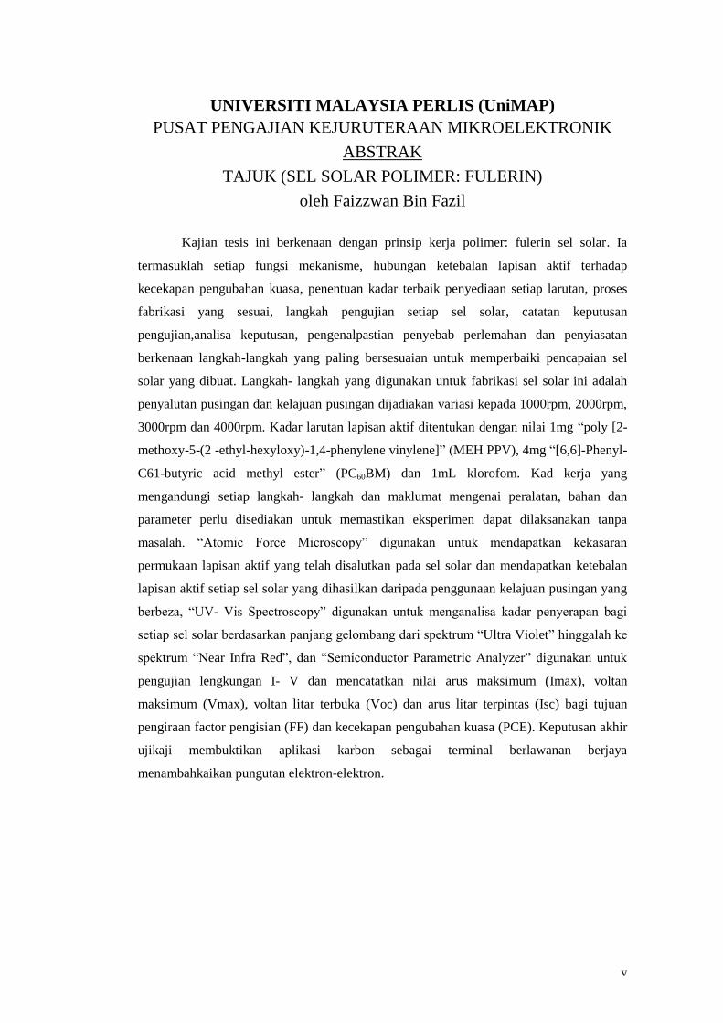
ABSTRAK
TAJUK (SEL SOLAR POLIMER: FULERIN)
oleh Faizzwan Bin Fazil
Kajian tesis ini berkenaan dengan prinsip kerja polimer: fulerin sel solar. Ia
termasuklah setiap fungsi mekanisme, hubungan ketebalan lapisan aktif terhadap
kecekapan pengubahan kuasa, penentuan kadar terbaik penyediaan setiap larutan, proses
fabrikasi yang sesuai, langkah pengujian setiap sel solar, catatan keputusan
pengujian,analisa keputusan, pengenalpastian penyebab perlemahan dan penyiasatan
berkenaan langkah-langkah yang paling bersesuaian untuk memperbaiki pencapaian sel
solar yang dibuat. Langkah- langkah yang digunakan untuk fabrikasi sel solar ini adalah
penyalutan pusingan dan kelajuan pusingan dijadiakan variasi kepada 1000rpm, 2000rpm,
3000rpm dan 4000rpm. Kadar larutan lapisan aktif ditentukan dengan nilai 1mg “poly [2-
methoxy-5-(2 -ethyl-hexyloxy)-1,4-phenylene vinylene]” (MEH PPV), 4mg “[6,6]-Phenyl-
C61-butyric acid methyl ester” (PC60BM) dan 1mL klorofom. Kad kerja yang
mengandungi setiap langkah- langkah dan maklumat mengenai peralatan, bahan dan
parameter perlu disediakan untuk memastikan eksperimen dapat dilaksanakan tanpa
masalah. “Atomic Force Microscopy” digunakan untuk mendapatkan kekasaran
permukaan lapisan aktif yang telah disalutkan pada sel solar dan mendapatkan ketebalan
lapisan aktif setiap sel solar yang dihasilkan daripada penggunaan kelajuan pusingan yang
berbeza, “UV- Vis Spectroscopy” digunakan untuk menganalisa kadar penyerapan bagi
setiap sel solar berdasarkan panjang gelombang dari spektrum “Ultra Violet” hinggalah ke
spektrum “Near Infra Red”, dan “Semiconductor Parametric Analyzer” digunakan untuk
pengujian lengkungan I- V dan mencatatkan nilai arus maksimum (Imax), voltan
maksimum (Vmax), voltan litar terbuka (Voc) dan arus litar terpintas (Isc) bagi tujuan
pengiraan factor pengisian (FF) dan kecekapan pengubahan kuasa (PCE). Keputusan akhir
ujikaji membuktikan aplikasi karbon sebagai terminal berlawanan berjaya
menambahkaikan pungutan elektron-elektron.
vi
UNIVERSITI MALAYSIA PERLIS (UniMAP)
SCHOOL OF MICROELECTRONIC ENGINEERING
ABSTRACT
POLYMER: FULLERINE SOLAR CELLS
by Faizzwan Bin Fazil
This study is about the about the polymer: fullerene (MEH PPV: PC60BM) solar
cells working principle including each mechanism, relation between thickness of the
active layer with the efficiency of power conversion, finest tune optimization, fabrication
process, devices inspection, results obtained, results analysis, error identification, and
investigation of the device enhancement method. The method used in fabricating the
devices is spin coating and the spin speed is varied to 1000rpm, 2000rpm, 3000rpm and
4000rpm. The tuning of the active layer solvent is fixed to 1mg of MEH PPV, 4mg of
PC60BM and 1mL of chloroform. The runcard which is consisted of every steps in
fabricating the devices is constructed in order to guide experimental process. Atomic Force
Microscopy (AFM) is used to inspect the surface roughness and the thickness of each
device, UV- Vis Spectroscopy is used to analyse the absorbance of each device from the
ultra violet (UV) spectrum till the near infra red (NIR) spectrum and the Semiconductor
Parametric Analyzer is used to inspect the I-V curve and record the maximum current
(Imax), maximum voltage (Vmax), open circuit voltage (Voc) and Isc for FF and PCE
evaluation purpose. The final result of experiment conducted proved the application of
carbon as a counter electrode enhances the electrons collection.
vii
Table of Contents
DECLARATION OF REPORT .................................................................... ii
DECLARATION SHEET ............................................................................ iii
Acknowledgement ....................................................................................... iv
ABSTRAK v
ABSTRACT vi
Table of Contents .................................................................................... vii
List of Tables x
List of Figures ............................................................................................ xi
List of Abbreviations ................................................................................. xiii
Chapter 1 Introduction ............................................................................. 1
1.1 Aims and motivation ................................................................................................................. 2
1.2 Objective of the experimental ................................................................................................... 3
1.3 Project Challenges .................................................................................................................... 3
1.4 Introduction of Inorganic Solar Cells ........................................................................................ 4
1.5 Introduction of Organic Solar Cells ..........................................................................................6
1.5.1 Introduction of Single Layer Cells..............................................................................6
1.5.2 Introduction of Bilayer Cells ......................................................................................8
1.5.3 Introduction of Bulk Heterojunction Cells ............................................................... 9
1.6 The Idea of Structuring the device ........................................................................................... 11
Chapter 2 Literature review .................................................................... 13
2.1 Introduction .............................................................................................................................. 13
2.2 Comparison of Nanostructured Material Processing using Different Chemical Techniques .. 14
2.2.1 The mainTechnique Used: Spin Coating ...................................................................17
2.3 Tuning Optimization ............................................................................................................... 20
2.3.1 MEH PPV: PCBM .................................................................................................... 20
viii
Figure 2.9 chemical structure of the reviewed MEH PPV: PCBM [38] .................................................21
Table 2.2 characteristic of MEH PPV: PCBM, P3HT: PCBM and PCDTBT: PCBM [35] ...................21
Figure 2.10 refractive indices of the reviewed P3HT: PCBM [18] ...................................................... 24
Figure 2.11 chemical structure of the reviewed P3HT: PCBM [33] .................................................... 24
Table 2.4 the parameters of P3HT: PCBM fabrication with the results reviewed ................................ 25
2.4 Safety Requirements ............................................................................................................... 28
2.5 Conclusion .............................................................................................................................. 29
Chapter 3 Methodology .......................................................................... 30
3.1 Introduction ............................................................................................................................. 30
3.2 Preparation of the Solvents based on the finest tuning ........................................................... 32
3.2.1 MEH PPV:PCBM ..................................................................................................... 32
3.3 Full Fabrication Process .......................................................................................................... 32
3.4 Conclusion .............................................................................................................................. 36
Chapter 4 Results and discussion ............................................................. 37
4.1 Introduction ............................................................................................................................. 37
4.1.1 Characterisation ........................................................................................................ 38
Table 4.1 Devices Characterisation ....................................................................................................... 38
4.1.2 Experimental results of UV-Visible λ evaluated based on the spin speeds: ............. 39
4.2 Conclusion .............................................................................................................................. 41
4.3 Experimental results I-V Curve evaluated based on the spin speeds: ..................................... 41
Figure 4.3 Typical I-V Curve for Solar Cells [50] ................................................................................ 42
Figure 4.4 I-V Curve obtained by each device ...................................................................................... 42
Table 4.2 The results obtained via SPA inspection (Plight is fixed) ..................................................... 43
Figure 4.5 I-V Curve obtained by a 1000RPM with carbon................................................................. 44
Table 4.3 The results obtained via SPA inspection (Plight is fixed) with carbon applied device ......... 45
4.4 Conclusion .............................................................................................................................. 45
Chapter 5 Business plan.......................................................................... 46
5.1 Introduction ............................................................................................................................ 46
5.2 Market analysis including effect on society and environment ............................................... 46
5.3 Business structure ................................................................................................................... 47
5.4 Costing ................................................................................................................................... 48
5.4.1 Capital cost .............................................................................................................. 48
5.4.2 Operational cost ........................................................................................................ 50
5.4.3 Material cost ............................................................................................................. 50

ix
5.5 Conclusion ...............................................................................................................................51
Chapter 6 Conclusion and future work .................................................... 52
6.1 Conclusion .............................................................................................................................. 52
6.2 Future work ............................................................................................................................. 54
List of publications ...................................................................................... 56
References 57

x
List of Tables
Table 2.1 Comparison of the method used in nanostructured material processing [14] .............. 16
Table 2.2 characteristic of MEH PPV: PCBM, P3HT: PCBM and PCDTBT: PCBM ...................... 21
Table 2.3 the parameters of MEH PPV: PCBM fabrication with the results reviewed ..................... 23
Table 2.5 the parameters of P3HT: PCBM fabrication with the results reviewed ............................ 25
Table 2.7 the parameters of PCDTBT: PCBM fabrication with the results reviewed .............. 27
Table 3.1 Predicted number of devices that required to be fabricated .............................................. 30
Table 4.1 Devices Characterisation ................................................................................................... 38
Table 4.2 The results obtained via SPA inspection (Plight is fixed) ................................................. 43
Table 4.3 The results obtained via SPA inspection (Plight is fixed) with carbon applied device ..... 45
Table 5.1 the minimum estimated price list of capital assets ....................................................... 50
Table 5.2 the price list of operational cost yearly ......................................................................... 50
Table 5.3 the price list of the materials used with available quantity ................................................. 51
xi
List of Figures
Figure 1.1 Phenomenon of EHP generation [51] ............................................................................ 4
Figure 1.2 Phenomenon of EHP diffusion [51] ............................................................................... 5
Figure 1.3 Phenomenon of EHP separation [51] ............................................................................ 5
Figure 1.4 Structure of Single layer cells [50] ................................................................................. 6
Figure 1.5 Phenomenon of EHP dissociation by Single Layer Cells [37] ..................................... 7
Figure 1.6 Structure of Bilayer cells [50]......................................................................................... 8
Figure 1.7 Phenomenon of EHP dissociation by Bilayer Cells [37]............................................... 9
Figure 1.8 Structure of Bulk Heterojunction Cells [50] ................................................................ 10
Figure 1.9 Phenomenon of EHP dissociation by Bulk Heterojunction Cells [37] ....................... 10
Figure 1.10 Structure of Bulk Heterojunction Polymer: Fullerene Solar Cells ........................... 11
Figure 2.1 alkylthiol modified nanoparticles onto bare Au [20] .................................................. 14
Figure 2.2 alkythiol modified surface under pure Au [20] ........................................................... 14
Figure 2.3 hydrolysis and condensation of a liquid precursor to a solid [20].............................. 16
Figure 2.4 Solution dispersion onto the substrate (ω = 0) [20] ..................................................... 17
Figure 2.5 Acceleration to its nominal rotation speed (dω/dt > 0) [20] ....................................... 17
Figure 2.6 Thinning of a liquid layer during rotation at a constant nominal speed dominating
by viscous force (dω/dt = 0) [20] ........................................................................................... 17
Figure 2.7 Hardening of the coating dominating by the solvent evaporation (dω/dt = 0) [20] .. 18
Figure 2.8 refractive indices of the reviewed MEH PPV: PCBM [19] ........................................ 20
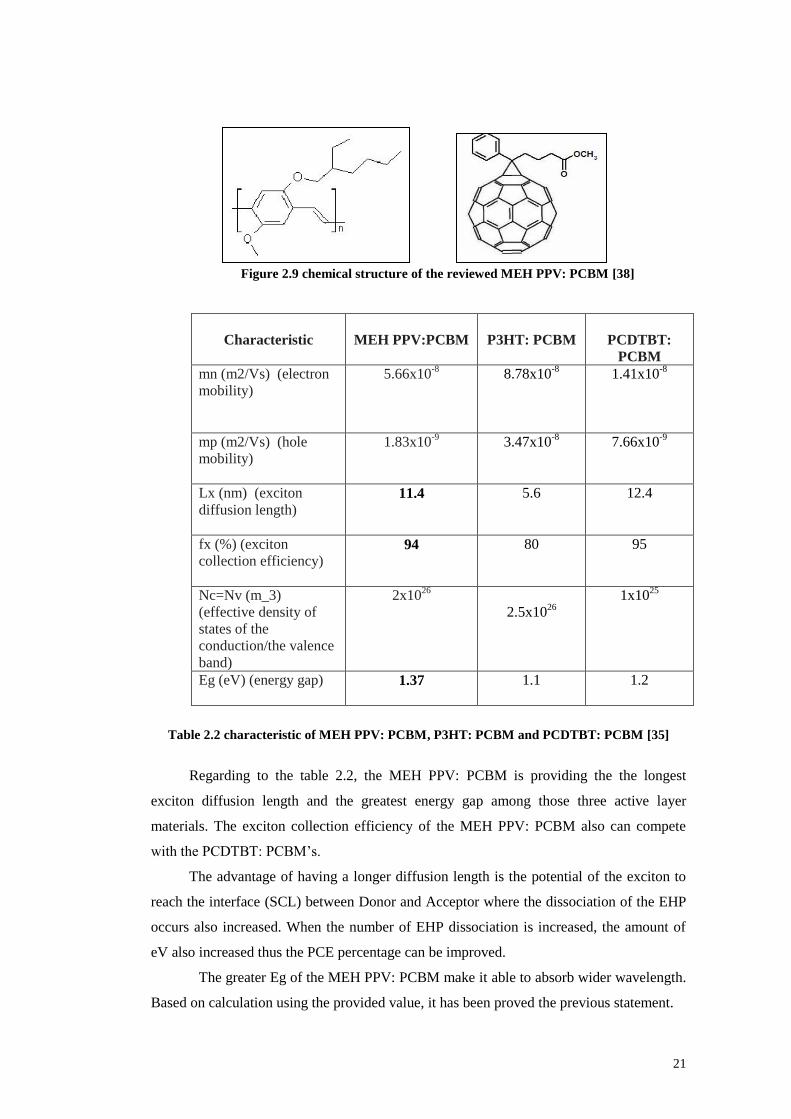
Figure 2.9 chemical structure of the reviewed MEH PPV: PCBM [38] ............................................. 21
Figure 2.10 refractive indices of the reviewed P3HT: PCBM [18] .................................................. 24
Figure 2.11 chemical structure of the reviewed P3HT: PCBM [33] ................................................ 24
Figure 2.12 chemical structure of the reviewed PCDTBT: PCBM [32] .................................... 26
Figure 3.1 Device fabrication steps ................................................................................................. 31
Figure 3.2 .......................................................................................................................................... 32
Figure 3.3 .......................................................................................................................................... 33
Figure 3.4 .......................................................................................................................................... 33
Figure 3.5 .......................................................................................................................................... 34
Figure 3.6 .......................................................................................................................................... 34
Figure 3.7 ......................................................................................................................................... 34
Figure 4.1 Electromagnetic Spectrum ........................................................................................... 39
Figure 4.2 UV-Vis Lambda Graph ................................................................................................ 40
Figure 4.3 Typical I-V Curve for Solar Cells [50] ............................................................................ 42
Figure 4.4 I-V Curve obtained by each device .................................................................................. 42
Figure 4.5 I-V Curve obtained by a 1000RPM with carbon.............................................................. 44
Figure 6.1 New structure of polymer: fullerene solar cells .......................................................... 53
Figure 6.2 ......................................................................................................................................... 54
Figure 6.3 ......................................................................................................................................... 54
Figure 6.4 ......................................................................................................................................... 54

xii
xiii
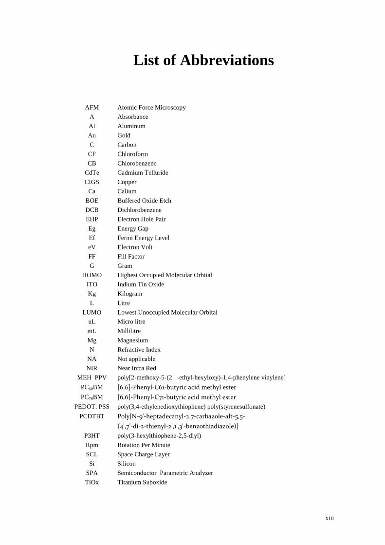
List of Abbreviations
AFM Atomic Force Microscopy
A Absorbance
Al Aluminum
Au Gold
C Carbon
CF Chloroform
CB Chlorobenzene
CdTe Cadmium Telluride
CIGS Copper
Ca Calium
BOE Buffered Oxide Etch
DCB Dichlorobenzene
EHP Electron Hole Pair
Eg Energy Gap
Ef Fermi Energy Level
eV Electron Volt
FF Fill Factor
G Gram
HOMO Highest Occupied Molecular Orbital
ITO Indium Tin Oxide
Kg Kilogram
L Litre
LUMO Lowest Unoccupied Molecular Orbital
uL Micro litre
mL Millilitre
Mg Magnesium
N Refractive Index
NA Not applicable
NIR Near Infra Red
MEH PPV poly[2-methoxy-5-(2�-ethyl-hexyloxy)-1,4-phenylene vinylene]
PC60BM [6,6]-Phenyl-C61-butyric acid methyl ester
PC70BM [6,6]-Phenyl-C71-butyric acid methyl ester
PEDOT: PSS poly(3,4-ethylenedioxythiophene) poly(styrenesulfonate)
PCDTBT Poly[N-9'-heptadecanyl-2,7-carbazole-alt-5,5-
(4',7'-di-2-thienyl-2',1',3'-benzothiadiazole)]
P3HT poly(3-hexylthiophene-2,5-diyl)
Rpm Rotation Per Minute
SCL Space Charge Layer
Si Silicon
SPA Semiconductor Parametric Analyzer
TiOx Titanium Suboxide

xiv
TiO2 Titanium Oxide
UV Ultra Violet
Vis Visible
1
Chapter 1 Introduction
Nowadays, a lot of development had been made in order to obtain high reliability,
green energy source with a reasonable capital cost. By replacing the non-renewable
electrical generating source such as fuel, charcoal and nuclear energy, photovoltaic device
also known as solar cell has been introduced which is operating to generate and dissociate
EHP by havesting photon shined by the sun. Generally, they are two types of solar cell
which are inorganic and organic solar cell.
In 1954, the 1st crystalline silicon solar cell was developed by Chapin, Fuller and
Pearson.[46] The highest efficiencies up to 25% was achieved by monocrystalline silicon
solar cell. However, the capital cost of production is very high. Another alternative is taken
which is producing a thin film solar cell from the material of inorganic such as CdTe
(Cadmium Telluride) or CIGS (Copper Indium Gallium Selenide) with the higest
efficiency obtained is around 16.7% to 19.%.[47] But these thin film solar cells are heavy
regarding to the usage of glass as protective layer; 1.2 m x 0.6 m modules weight 12.0
kg.[48]
The basic principal of a typical silicon solar cell is the absorption of photon also
considered as EHP (electron hole pair) or exciton into the the device and the EHP is
moving towards the SCL (space charge layer) also known as depletion region from both
side, the P side which side is excess with positively charge, holes and the N side which is
excess with negatively charge, electrons. Due to a huge potential different between P side
and N side, electric field is occurred. In depletion region, the EHP is dissociated where
electron is separated to the conduction band at the same time moving to the cathode, and
hole is moving towards anode and energy in form of electron volt (eV) is produced.
For the organic solar cell is totally different compared to inorganic solar cell. This
solar cell was developed specially to reduce the capital cost of production, at the same time
the avaibility of the material is very high. There’s a lot of investigation of this solar cell
have been made in order to increase the low efficiency obtained till the development made
by Solarmer Energy which was achieving 8.13% efficiency in 2010.[49] The efforts of
researching the method of increasing the efficiency never stopped. The experimental using
polymer:fullerene as active layer, the morphology of the active layer whether fabricated in
form of single layer, bilayer or bulk hetero junction, the materials used as active layer with
2
the suitable dilution, and the suitable and low cost fabrication method being used have
been made.
1.1 Aims and motivation
In order to produce a reliable and efficient organic solar cell, they are several
elements that need to be considered properly. By referring to the basic principle of organic
solar cell such as the absorption of photon, exciton (electron-hole pair) diffusion, exciton
(electron-hole pair) dissociation,and the electron and hole mobility towards electrodes; the
elements that need to be put as main priority are determined.
Photon absorbed in Polymer: fullerene active layer will excite electrons to a state
above band gap and forming exciton. Columbic attraction forces are tightly binding the
hole and electron in this state (0.3-1eV). To collect as much as possible the exciton, the
light trapping system might be needed to be mounted on the top of glass surface so the
incident photon reflected on the top surface can be reduced which mean the absorption of
the photon is increased.
Before vanishing, the polymer in range of 10nm can be diffused through by the
exciton. Bulk heterojunction active layer is introduced where the distance between
polymer (electron donor) and fullerene (electron acceptor) can be minized. The donor and
the acceptor material are everywhere in the layer so the interfaces also are at everywhere.
So, the EHP is easily diffused to the interface between donor and acceptor. In order to
obtain free charge carriers before vanishing, It requires the energy of electric field which
must be greater than exciton binding energy, in other words, must be greater than 0.4eV to
break that exciton binding. Thus, electron and hole will be dissociated apart.
After dissociation occurred, the free charges obtained need to be mobilized to the
electrode. This step is important to trap the entire dissociated free charge carrier. The
material used will determine the efficiency of hole harvesting at anode, electron harvesting
at cathode. That’s why TiOx is used as hole blocker from collected by cathode and
PEDOT: PSS is used because it is good at conducting hole so it will allow hole to move to
anode easily.
All of this additional elements will be investigated their performance in the
experiments. The structure and the materials might be changed if it couldn’t perform well
in the results. The volume of solvents and another ingredients also will play major role in
the experiment due to the limited material and equipment.
3
1.2 Objective of the experimental
There are several purposes of conducting these experimental. The spin speeds of
spin coating deposition for active layer (polymer: fullerene layer) need to be varied to
1000RPM, 2000RPM, 3000RPM and 4000RPM. The purpose is to relate the the relation
between the thicknesses obtained using the Atomic Force Microscopy (AFM) after the
application of those various spin speed with the absorbance which is obtained by using the
UV- Vis Spectroscopy and the PCE obtained using the SPA which provide several reading
for PCE evaluation purpose. Among those spin speed, which device fabricated providing
the best performance is the milestone of this experimental purpose.
Besides investigating the effect of varied spin speeds on depositing the active layer,
another parameter of the material also has to be reviewed and fixed for the poly(3,4-
ethylenedioxythiophene) poly(styrenesulfonate) (PEDOT: PSS) solvent deposition, the
temperature with annealing duration, and the weight ratio of polymer: fullerene with
suitable dilution. Eventhough this study is out from the experimental conduct but a robust,
proper tuning is required to minimize the undesired result.
Another additional component that will be introduced in this experiment is the usage
of Titanium Oxide (TiO2) as the holes blocker and the usage of Indium Tin Oxide (ITO)
coated glass as cathode by replacing the Aluminum (Al). The outcome of this application
will be observed whether it can bring the improvement or not. If it fails to improve the
perfoemance, proper solution is required to overcome the failure. But the application of the
ITO as a replacement for the Al is a must due to fabricate the simple and affordable device.
1.3 Project Challenges
Eventhough polymer: fullerene solar cell is easier to be fabricated and require lower
cost compared to inorganic solar cell, the material itself is highly sensitive to H20 and O2.
The samples might degrade either during fabrication process or inspection process where
the samples are exposed to the mentioned causes.
The deposited PEDOT: PSS might be dissolved with the H2O left on the ITO
surface if the cleaned ITO coated glass is not dried thoroughly. When the deposited
PEDOT: PSS dissolved with the water, the holes transportation potential of its will be
degraded and will affect the performance of power conversion to be weakened.
The application of the ITO as a substituent for Al also might result a poor result due
to its electron mobility is not as good as Al’s. The experiment of studying this process
4
might be worthwhile due to the fresh idea of innovation new fabrication method
eventhough the becoming results will be not good as using the Al.
The insufficient material of PCBM is the biggest challenge in this experiment. The
amount of PCBM purchased is just 1g for a bottle. The price is about RM900 and the
shipping of the item takes a lot of time. Due to the highest efficiency obtained by 1: 4
weight ratio of polymer: fullerene, so it requires greater amount of fullerene which is 4
times more than polymer for fabricating those devices.
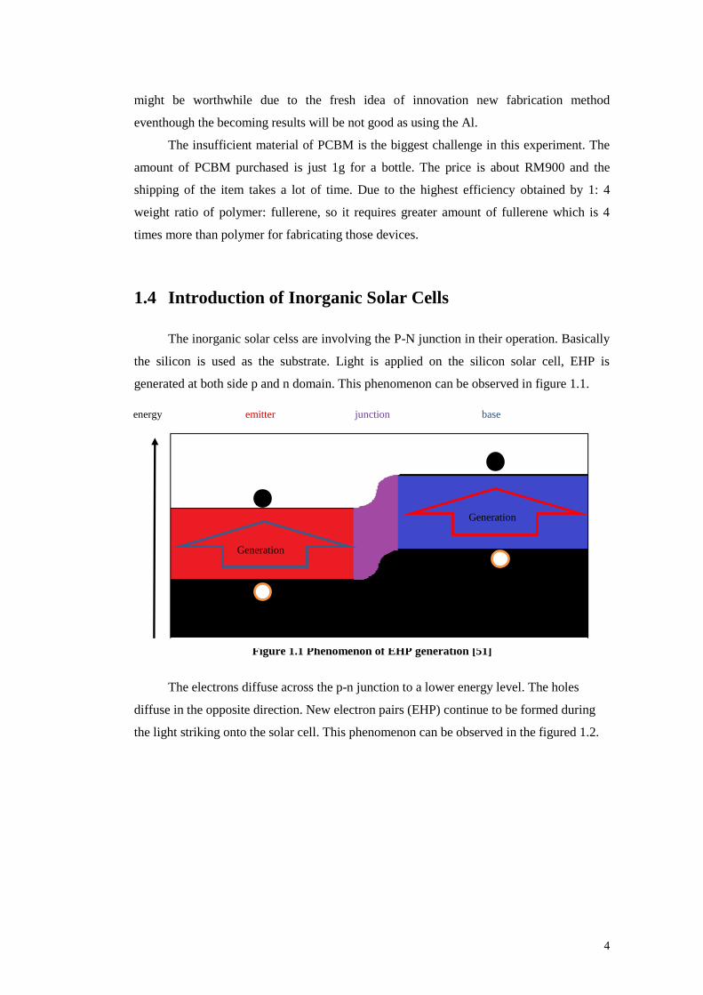
1.4 Introduction of Inorganic Solar Cells
The inorganic solar celss are involving the P-N junction in their operation. Basically
the silicon is used as the substrate. Light is applied on the silicon solar cell, EHP is
generated at both side p and n domain. This phenomenon can be observed in figure 1.1.
Figure 1.1 Phenomenon of EHP generation [51]
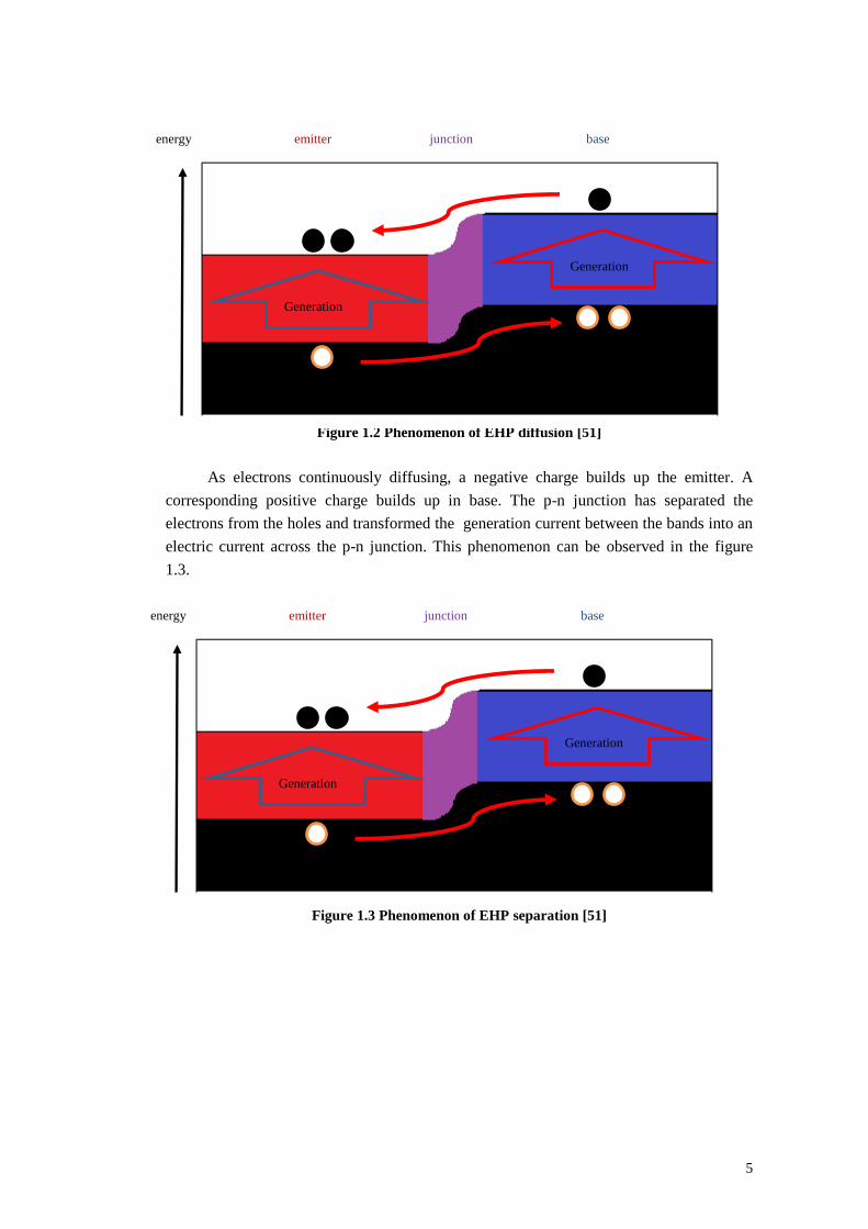
The electrons diffuse across the p-n junction to a lower energy level. The holes
diffuse in the opposite direction. New electron pairs (EHP) continue to be formed during
the light striking onto the solar cell. This phenomenon can be observed in the figured 1.2.
Generation
Generation
energy emitter junction base
5
Figure 1.2 Phenomenon of EHP diffusion [51]
As electrons continuously diffusing, a negative charge builds up the emitter. A
corresponding positive charge builds up in base. The p-n junction has separated the
electrons from the holes and transformed the generation current between the bands into an
electric current across the p-n junction. This phenomenon can be observed in the figure
1.3.
Figure 1.3 Phenomenon of EHP separation [51]
Generation
Generation
energy emitter junction base
Generation
Generation
energy emitter junction base
6
1.5 Introduction of Organic Solar Cells
Organic solar cells are totally different compared to inorganic semiconductor
solar cells in terms of structure. But for the working principal, both are approximately the
same. The difference is the inorganic solar cells are using the P-N junction with the
valance and concuction band while the organic solar cells are using Donor –Acceptor with
the HOMO (Highest Occupied Molecular Orbital) and the LUMO (Lowest Unoccupied
Molecular Orbital). Organic solar cell also provide one biggest advantage which is it can
be fabricate on the flexible substrate. It can be intergrated onto clothing, bagpack and very
versatile. The capital cost also is reasonable compare to the inorganic solar cell.
Organic solar cells were founded built with a single active layer, followed by
bilayer active layer, and recently, bulk heterojunction active layer.
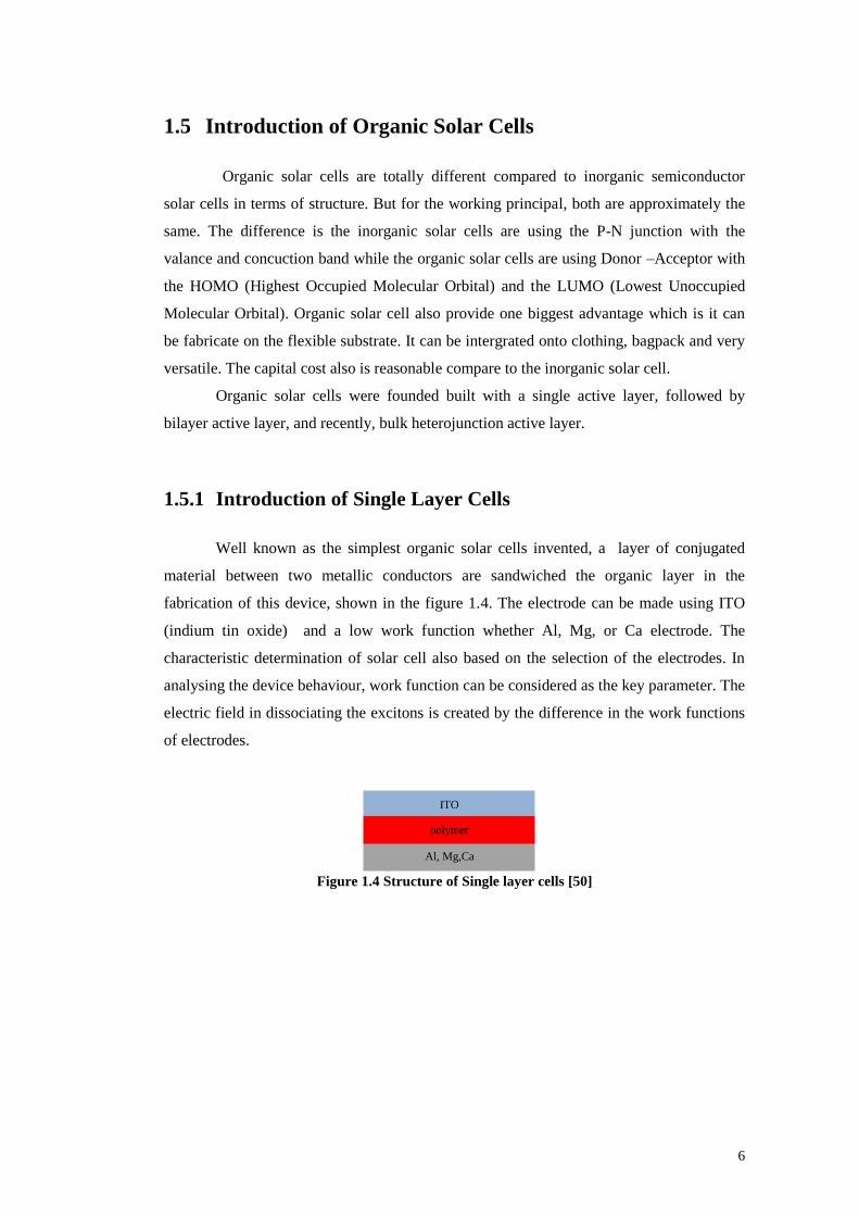
1.5.1 Introduction of Single Layer Cells
Well known as the simplest organic solar cells invented, a layer of conjugated
material between two metallic conductors are sandwiched the organic layer in the
fabrication of this device, shown in the figure 1.4. The electrode can be made using ITO
(indium tin oxide) and a low work function whether Al, Mg, or Ca electrode. The
characteristic determination of solar cell also based on the selection of the electrodes. In
analysing the device behaviour, work function can be considered as the key parameter. The
electric field in dissociating the excitons is created by the difference in the work functions
of electrodes.
Figure 1.4 Structure of Single layer cells [50]
Al, Mg,Ca
polymer
ITO
7
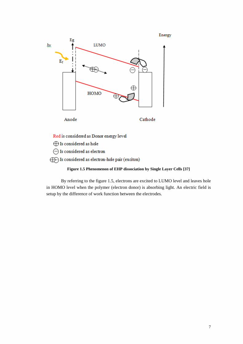
Figure 1.5 Phenomenon of EHP dissociation by Single Layer Cells [37]
By referring to the figure 1.5, electrons are excited to LUMO level and leaves hole
in HOMO level when the polymer (electron donor) is absorbing light. An electric field is
setup by the difference of work function between the electrodes.
8
1.5.2 Introduction of Bilayer Cells
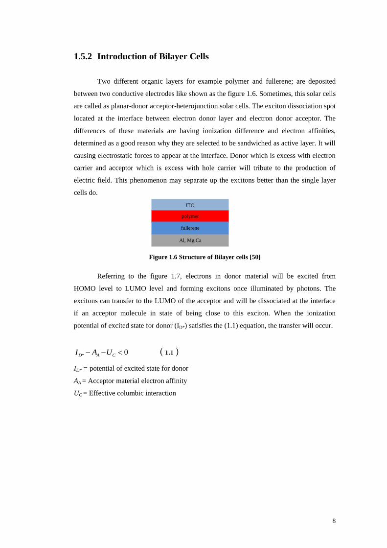
Two different organic layers for example polymer and fullerene; are deposited
between two conductive electrodes like shown as the figure 1.6. Sometimes, this solar cells
are called as planar-donor acceptor-heterojunction solar cells. The exciton dissociation spot
located at the interface between electron donor layer and electron donor acceptor. The
differences of these materials are having ionization difference and electron affinities,
determined as a good reason why they are selected to be sandwiched as active layer. It will
causing electrostatic forces to appear at the interface. Donor which is excess with electron
carrier and acceptor which is excess with hole carrier will tribute to the production of
electric field. This phenomenon may separate up the excitons better than the single layer
cells do.
Figure 1.6 Structure of Bilayer cells [50]
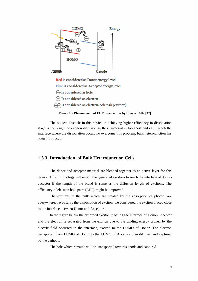
Referring to the figure 1.7, electrons in donor material will be excited from
HOMO level to LUMO level and forming excitons once illuminated by photons. The
excitons can transfer to the LUMO of the acceptor and will be dissociated at the interface
if an acceptor molecule in state of being close to this exciton. When the ionization
potential of excited state for donor (ID*) satisfies the (1.1) equation, the transfer will occur.
* 0D A CI A U ( 1.1 )
ID* = potential of excited state for donor
AA = Acceptor material electron affinity
UC = Effective columbic interaction
Al, Mg,Ca
polymer
fullerene
ITO
9
Figure 1.7 Phenomenon of EHP dissociation by Bilayer Cells [37]
The biggest obstacle in this device in achieving higher efficiency in dissociation
stage is the length of exciton diffusion in these material is too short and can’t reach the
interface where the dissociation occur. To overcome this problem, bulk heterojunction has
been introduced.
1.5.3 Introduction of Bulk Heterojunction Cells
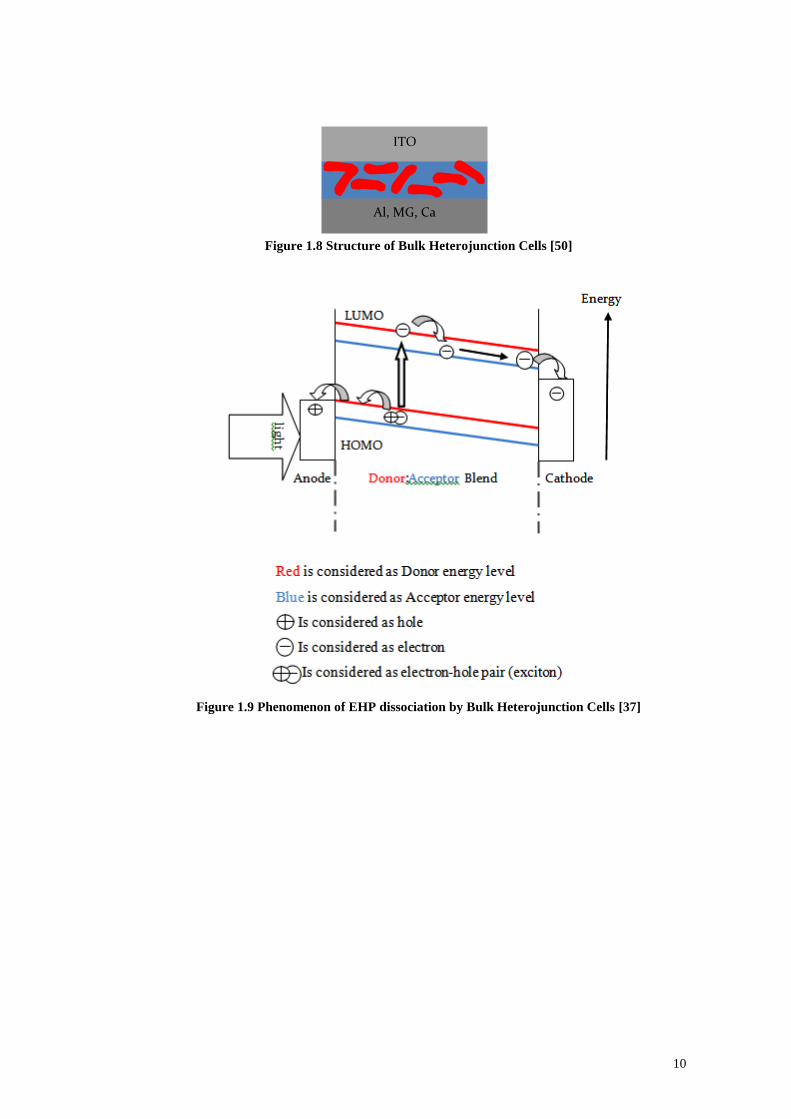
The donor and acceptor material are blended together as an active layer for this
device. This morphology will enrich the generated excitons to reach the interface of donor-
acceptor if the length of the blend is same as the diffusion length of excitons. The
efficiency of electron hole pairs (EHP) might be improved.
The excitons in the bulk which are created by the absorption of photon, are
everywhere. To observe the dissociation of exciton, we considered the exciton placed close
to the interface between Donor and Acceptor.
In the figure below the absorbed exciton reaching the interface of Donor-Acceptor
and the electron is separated from the exciton due to the binding energy broken by the
electric field occurred in the interface, excited to the LUMO of Donor. The electron
transported from LUMO of Donor to the LUMO of Acceptor then diffused and captured
by the cathode.
The hole which remains will be transported towards anode and captured.
10
Figure 1.8 Structure of Bulk Heterojunction Cells [50]
Figure 1.9 Phenomenon of EHP dissociation by Bulk Heterojunction Cells [37]
ITO
Al, MG, Ca
11
1.6 The Idea of Structuring the device
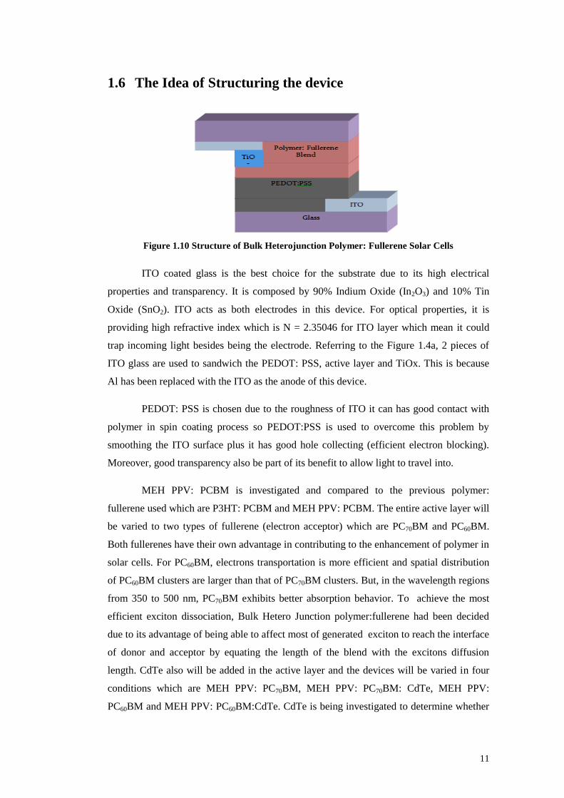
Figure 1.10 Structure of Bulk Heterojunction Polymer: Fullerene Solar Cells
ITO coated glass is the best choice for the substrate due to its high electrical
properties and transparency. It is composed by 90% Indium Oxide (In2O3) and 10% Tin
Oxide (SnO2). ITO acts as both electrodes in this device. For optical properties, it is
providing high refractive index which is N = 2.35046 for ITO layer which mean it could
trap incoming light besides being the electrode. Referring to the Figure 1.4a, 2 pieces of
ITO glass are used to sandwich the PEDOT: PSS, active layer and TiOx. This is because
Al has been replaced with the ITO as the anode of this device.
PEDOT: PSS is chosen due to the roughness of ITO it can has good contact with
polymer in spin coating process so PEDOT:PSS is used to overcome this problem by
smoothing the ITO surface plus it has good hole collecting (efficient electron blocking).
Moreover, good transparency also be part of its benefit to allow light to travel into.
MEH PPV: PCBM is investigated and compared to the previous polymer:
fullerene used which are P3HT: PCBM and MEH PPV: PCBM. The entire active layer will
be varied to two types of fullerene (electron acceptor) which are PC70BM and PC60BM.
Both fullerenes have their own advantage in contributing to the enhancement of polymer in
solar cells. For PC60BM, electrons transportation is more efficient and spatial distribution
of PC60BM clusters are larger than that of PC70BM clusters. But, in the wavelength regions
from 350 to 500 nm, PC70BM exhibits better absorption behavior. To achieve the most
efficient exciton dissociation, Bulk Hetero Junction polymer:fullerene had been decided
due to its advantage of being able to affect most of generated exciton to reach the interface
of donor and acceptor by equating the length of the blend with the excitons diffusion
length. CdTe also will be added in the active layer and the devices will be varied in four
conditions which are MEH PPV: PC70BM, MEH PPV: PC70BM: CdTe, MEH PPV:
PC60BM and MEH PPV: PC60BM:CdTe. CdTe is being investigated to determine whether

12
it can provide a nano-scale interpenetrating network of electron donor and electron
acceptor.
TiOx (Titanium Suboxide) is used as an optical spacer to gain greater light
absorption (it has high refractive index) by breaking the symmetry and blocking hole
(electron collecting). It is also can reduce “dead layer”. It is placed between Al and active
layer to comprise phase separated blend.
13
Chapter 2 Literature review
2.1 Introduction
In order to fabricate the device with obtaining reasonable result, it requires the
appropriate techniques of fabrication and tools handling, robust knowledge of the
characterization of the materials used to find the finest tune of solvent involved and the
condition of the workplace.
In choosing the appropriate techniques, there’s several condition need to be
considered such as adhesion, thermal stability, mechanical properties, thickness precision,
level of ordering and industrial compatibility.
The architecture of polymer:fullerene morphology also plays major role in order to
harvest as much as possible excitons, to trap them inside, to maximize the the exciton
diffusion length or minimize the distance of interface between electron donor and electron
acceptor, to increase electron and hole towards electrode, and the morphology of active
layer whether bilayer form, heterojunction or bulk heterojunction. Last but not least, it
requires to use the finest tune of solvent to create a device.
Besides putting the results as main priority, the safety tips also need to be followed
to avoid any undesired incident happen. This is important especially dealing with
hazardous material.
14
2.2 Comparison of Nanostructured Material Processing using
Different Chemical Techniques
There are multiple ways of depositing a colloid nanoparticles onto the solid
substrate..It can be categorised into 5 techniques which are Electro-deposition, Chemical
Self-Assembly, Electrostatic, Langmuir-Blodgett and Spin Coating.
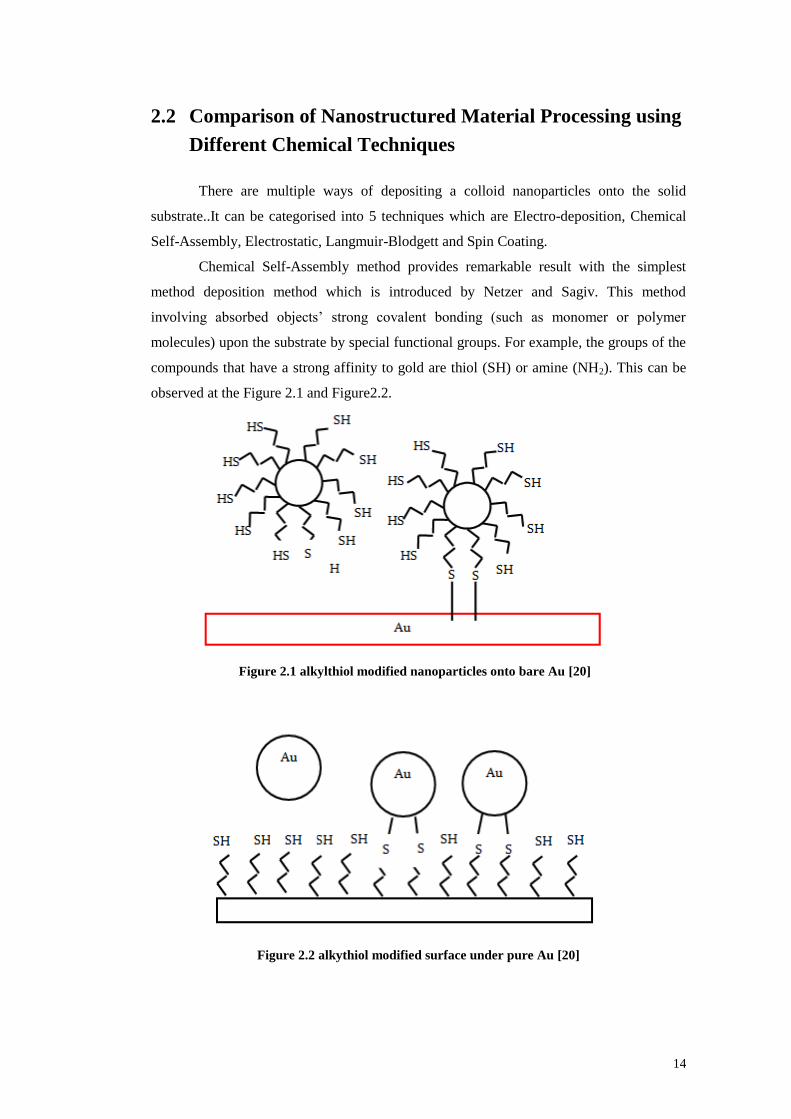
Chemical Self-Assembly method provides remarkable result with the simplest
method deposition method which is introduced by Netzer and Sagiv. This method
involving absorbed objects’ strong covalent bonding (such as monomer or polymer
molecules) upon the substrate by special functional groups. For example, the groups of the
compounds that have a strong affinity to gold are thiol (SH) or amine (NH2). This can be
observed at the Figure 2.1 and Figure2.2.
Figure 2.1 alkylthiol modified nanoparticles onto bare Au [20]
Figure 2.2 alkythiol modified surface under pure Au [20]
15
Electrodeposition is one of the earliest methods for depositing inorganic coating on
the solid surface. It has two types of electrodepositions which are the combination of the
formation for stabilized colloids particle with their electrodeposition and electrodeposition
of preformed colloid nanoparticles. Somekind of surfactant should be added to the
electrolyte solution in order to form nanostructured material. Nanocrystals are coated and
prevented from further aggregation by the surfactants which act as stabilizing agent. The
role of the substrate is very important factor of adhesive percentage in elctrodeposition.
The growth of monodispersed nanoclusters can be stimulated due to highly ordered
substrate surfaces. A variety of materials including metals, semiconductors, ceramics and
polymers could be deposited using this method.[20]
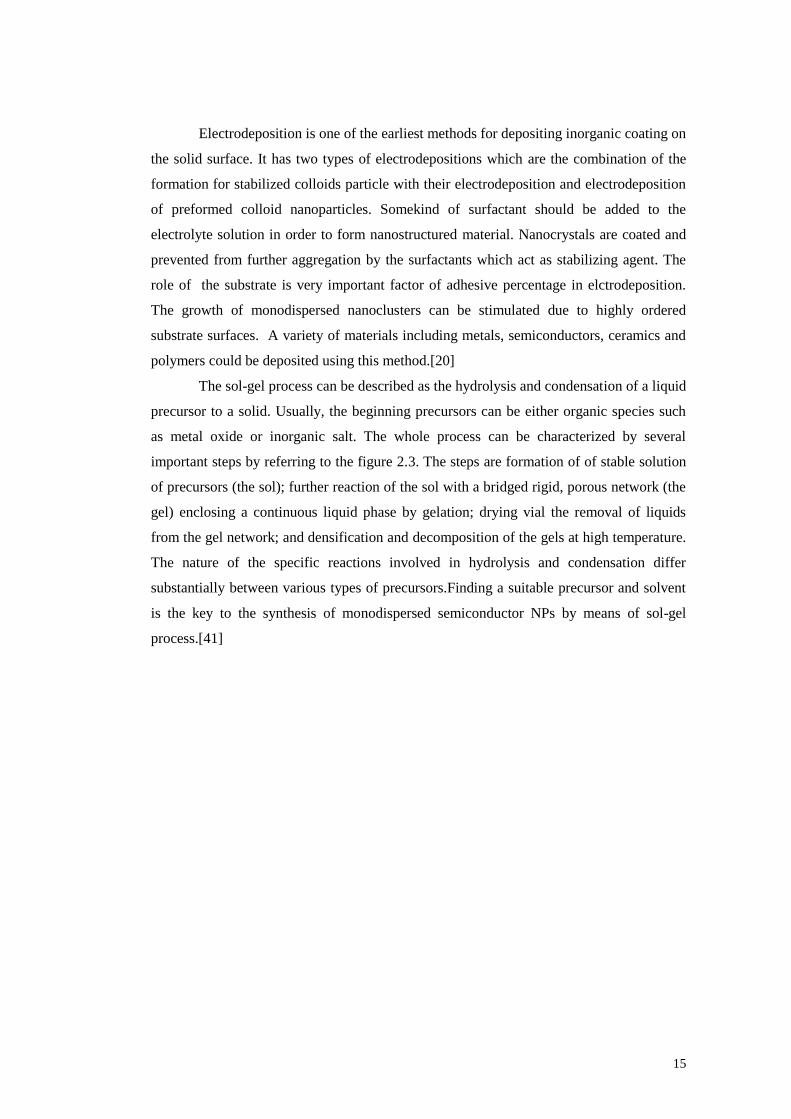
The sol-gel process can be described as the hydrolysis and condensation of a liquid
precursor to a solid. Usually, the beginning precursors can be either organic species such
as metal oxide or inorganic salt. The whole process can be characterized by several
important steps by referring to the figure 2.3. The steps are formation of of stable solution
of precursors (the sol); further reaction of the sol with a bridged rigid, porous network (the
gel) enclosing a continuous liquid phase by gelation; drying vial the removal of liquids
from the gel network; and densification and decomposition of the gels at high temperature.
The nature of the specific reactions involved in hydrolysis and condensation differ
substantially between various types of precursors.Finding a suitable precursor and solvent
is the key to the synthesis of monodispersed semiconductor NPs by means of sol-gel
process.[41]
16
Figure 2.3 hydrolysis and condensation of a liquid precursor to a solid [20]
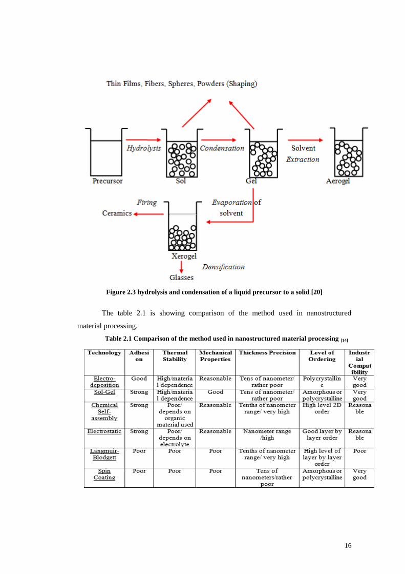
The table 2.1 is showing comparison of the method used in nanostructured
material processing.
Table 2.1 Comparison of the method used in nanostructured material processing [14]
17
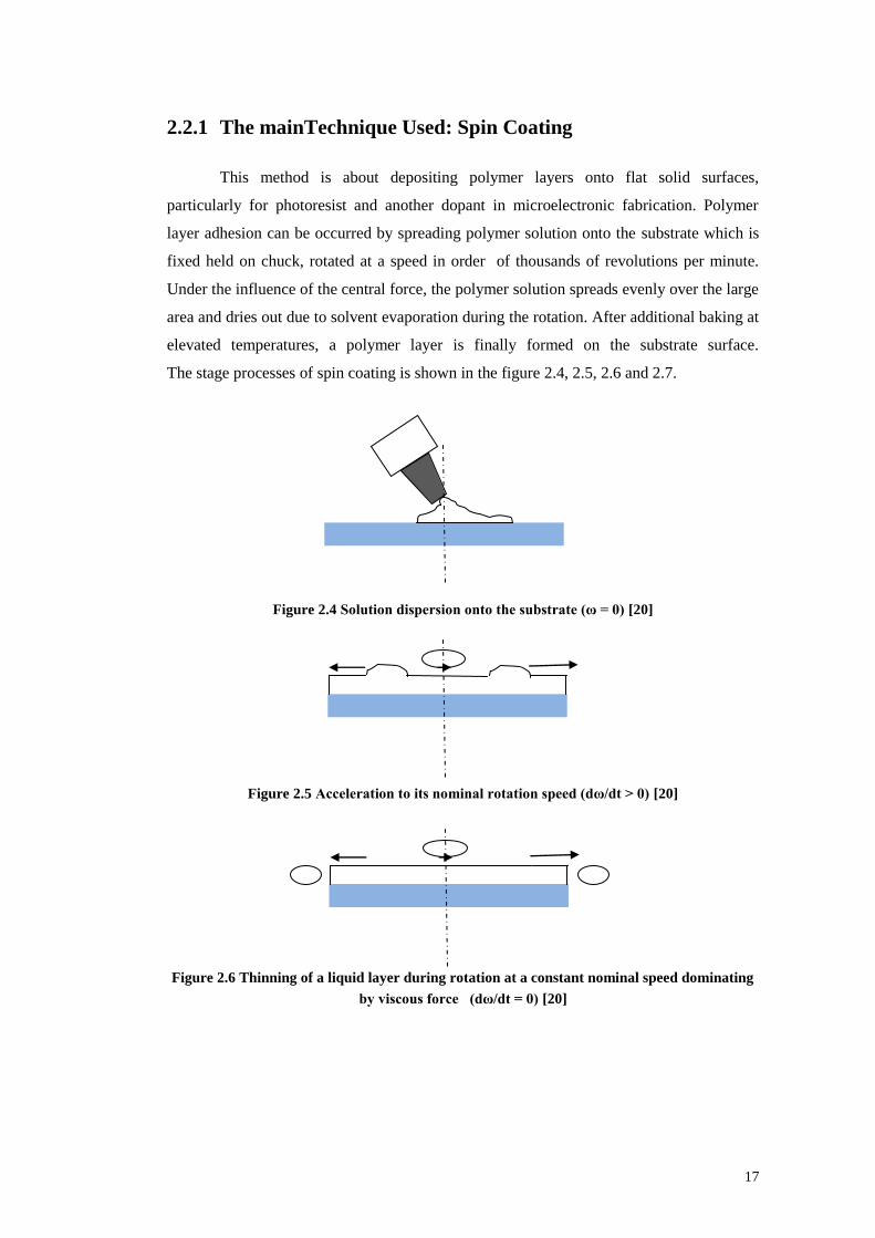
2.2.1 The mainTechnique Used: Spin Coating
This method is about depositing polymer layers onto flat solid surfaces,
particularly for photoresist and another dopant in microelectronic fabrication. Polymer
layer adhesion can be occurred by spreading polymer solution onto the substrate which is
fixed held on chuck, rotated at a speed in order of thousands of revolutions per minute.
Under the influence of the central force, the polymer solution spreads evenly over the large
area and dries out due to solvent evaporation during the rotation. After additional baking at
elevated temperatures, a polymer layer is finally formed on the substrate surface.
The stage processes of spin coating is shown in the figure 2.4, 2.5, 2.6 and 2.7.
Figure 2.4 Solution dispersion onto the substrate (ω = 0) [20]
Figure 2.5 Acceleration to its nominal rotation speed (dω/dt > 0) [20]
Figure 2.6 Thinning of a liquid layer during rotation at a constant nominal speed dominating
by viscous force (dω/dt = 0) [20]
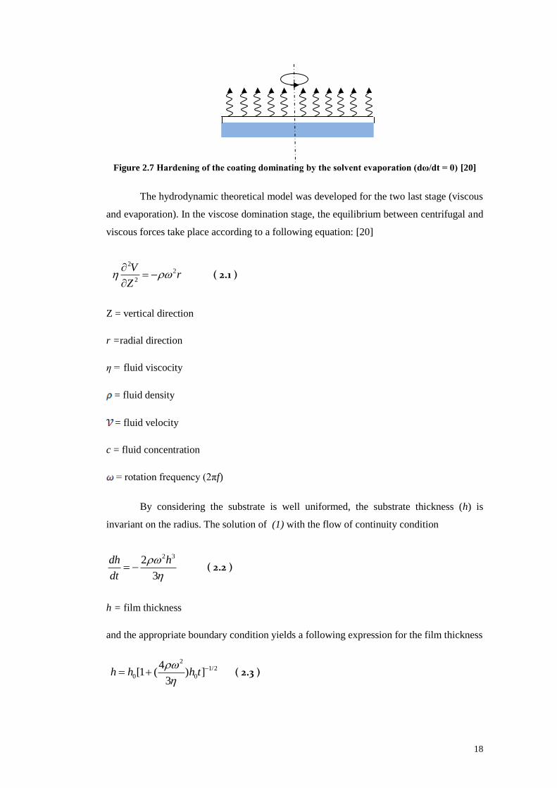
18
Figure 2.7 Hardening of the coating dominating by the solvent evaporation (dω/dt = 0) [20]
The hydrodynamic theoretical model was developed for the two last stage (viscous
and evaporation). In the viscose domination stage, the equilibrium between centrifugal and
viscous forces take place according to a following equation: [20]
2
2
2
Vr
Z
( 2.1 )
Z = vertical direction
r =radial direction
η = fluid viscocity
= fluid density
= fluid velocity
c = fluid concentration
= rotation frequency (2πf)
By considering the substrate is well uniformed, the substrate thickness (h) is
invariant on the radius. The solution of (1) with the flow of continuity condition
2 32
3
dh h
dt
( 2.2 )
h = film thickness
and the appropriate boundary condition yields a following expression for the film thickness
21/2
0 0
4[1 ( ) ]
3h h h t
( 2.3 )
19
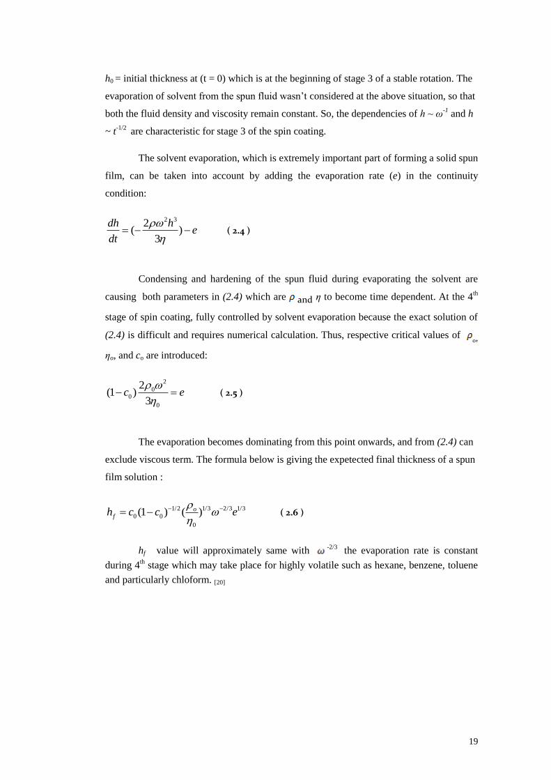
h0 = initial thickness at (t = 0) which is at the beginning of stage 3 of a stable rotation. The
evaporation of solvent from the spun fluid wasn’t considered at the above situation, so that
both the fluid density and viscosity remain constant. So, the dependencies of h ~ ω-1
and h
~ t-1/2
are characteristic for stage 3 of the spin coating.
The solvent evaporation, which is extremely important part of forming a solid spun
film, can be taken into account by adding the evaporation rate (e) in the continuity
condition:
2 32( )
3
dh he
dt
( 2.4 )
Condensing and hardening of the spun fluid during evaporating the solvent are
causing both parameters in (2.4) which are and η to become time dependent. At the 4th
stage of spin coating, fully controlled by solvent evaporation because the exact solution of
(2.4) is difficult and requires numerical calculation. Thus, respective critical values of o,
ηo, and co are introduced:
2
00
0
2(1 )
3c e
( 2.5 )
The evaporation becomes dominating from this point onwards, and from (2.4) can
exclude viscous term. The formula below is giving the expetected final thickness of a spun
film solution :
1/2 1/3 2/3 1/3
0 0
0
(1 ) ( )ofh c c e
( 2.6 )
hf value will approximately same with -2/3
the evaporation rate is constant
during 4th stage which may take place for highly volatile such as hexane, benzene, toluene
and particularly chloform. [20]
20
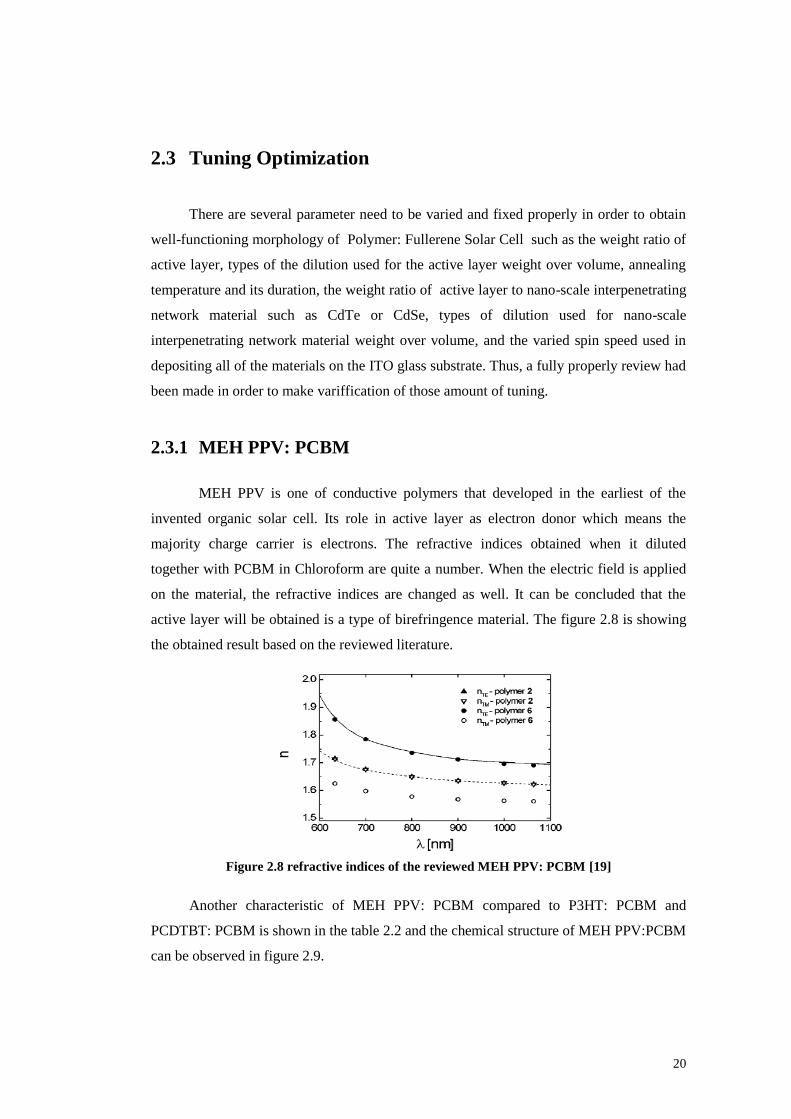
2.3 Tuning Optimization
There are several parameter need to be varied and fixed properly in order to obtain
well-functioning morphology of Polymer: Fullerene Solar Cell such as the weight ratio of
active layer, types of the dilution used for the active layer weight over volume, annealing
temperature and its duration, the weight ratio of active layer to nano-scale interpenetrating
network material such as CdTe or CdSe, types of dilution used for nano-scale
interpenetrating network material weight over volume, and the varied spin speed used in
depositing all of the materials on the ITO glass substrate. Thus, a fully properly review had
been made in order to make variffication of those amount of tuning.
2.3.1 MEH PPV: PCBM
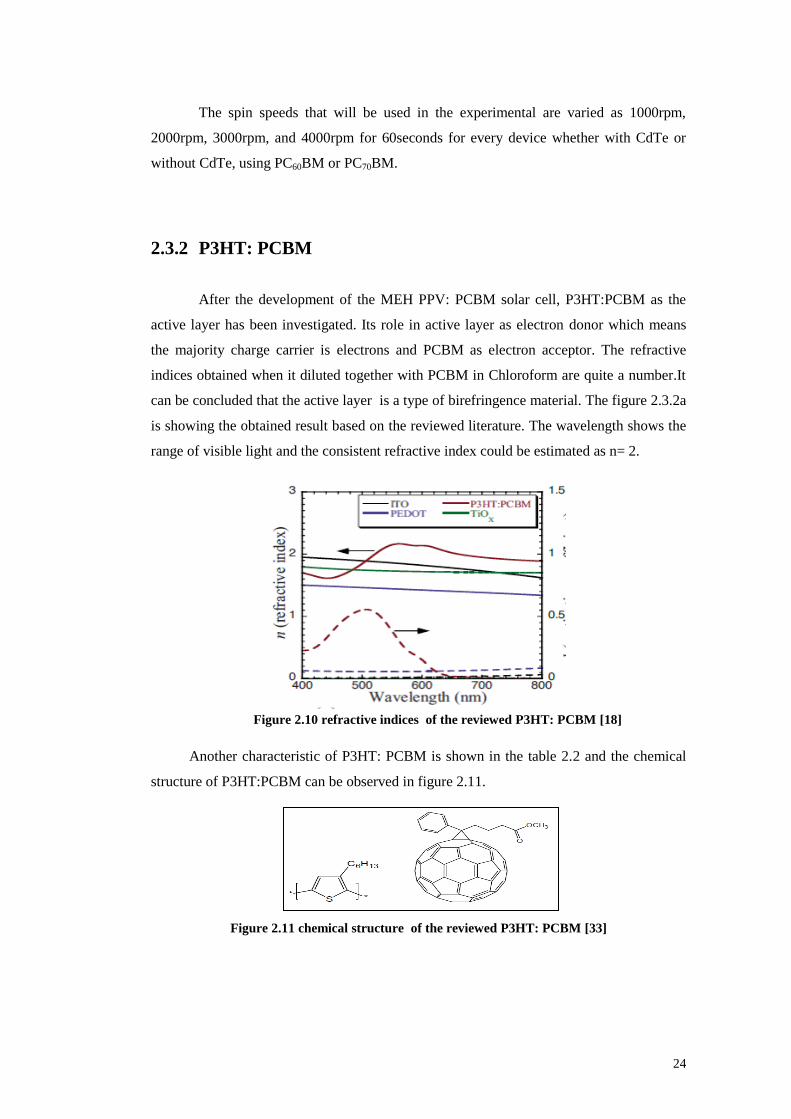
MEH PPV is one of conductive polymers that developed in the earliest of the
invented organic solar cell. Its role in active layer as electron donor which means the
majority charge carrier is electrons. The refractive indices obtained when it diluted
together with PCBM in Chloroform are quite a number. When the electric field is applied
on the material, the refractive indices are changed as well. It can be concluded that the
active layer will be obtained is a type of birefringence material. The figure 2.8 is showing
the obtained result based on the reviewed literature.
Figure 2.8 refractive indices of the reviewed MEH PPV: PCBM [19]
Another characteristic of MEH PPV: PCBM compared to P3HT: PCBM and
PCDTBT: PCBM is shown in the table 2.2 and the chemical structure of MEH PPV:PCBM
can be observed in figure 2.9.
21
Figure 2.9 chemical structure of the reviewed MEH PPV: PCBM [38]
Characteristic
MEH PPV:PCBM
P3HT: PCBM
PCDTBT:
PCBM
mn (m2/Vs) (electron
mobility)
5.66x10⁻⁸
8.78x10⁻⁸
1.41x10⁻⁸
mp (m2/Vs) (hole
mobility)
1.83x10⁻⁹
3.47x10⁻⁸
7.66x10⁻⁹
Lx (nm) (exciton
diffusion length)
11.4
5.6 12.4
fx (%) (exciton
collection efficiency)
94
80 95
Nc=Nv (m_3)
(effective density of
states of the
conduction/the valence
band)
2x1026
2.5x1026
1x1025
Eg (eV) (energy gap)
1.37
1.1 1.2
Table 2.2 characteristic of MEH PPV: PCBM, P3HT: PCBM and PCDTBT: PCBM [35]
Regarding to the table 2.2, the MEH PPV: PCBM is providing the the longest
exciton diffusion length and the greatest energy gap among those three active layer
materials. The exciton collection efficiency of the MEH PPV: PCBM also can compete
with the PCDTBT: PCBM’s.
The advantage of having a longer diffusion length is the potential of the exciton to
reach the interface (SCL) between Donor and Acceptor where the dissociation of the EHP
occurs also increased. When the number of EHP dissociation is increased, the amount of
eV also increased thus the PCE percentage can be improved.
The greater Eg of the MEH PPV: PCBM make it able to absorb wider wavelength.
Based on calculation using the provided value, it has been proved the previous statement.
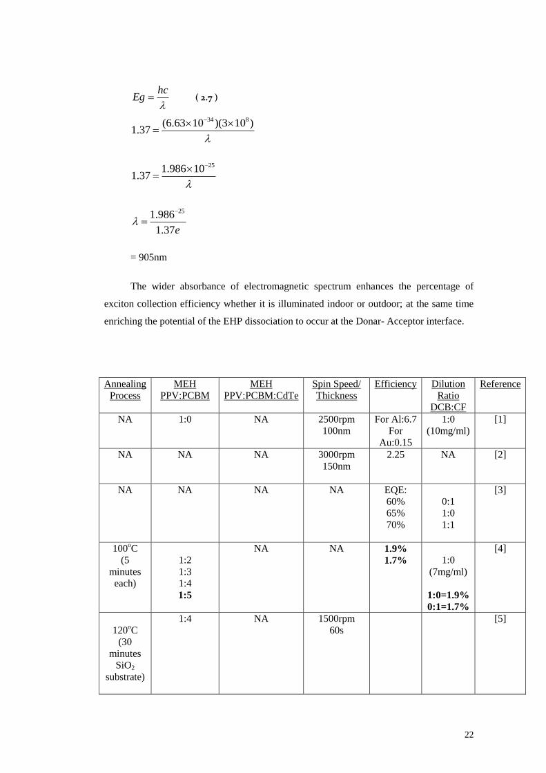
22
hcEg
( 2.7 )
34 8(6.63 10 )(3 10 )1.37
251.986 10
1.37
251.986
1.37e
= 905nm
The wider absorbance of electromagnetic spectrum enhances the percentage of
exciton collection efficiency whether it is illuminated indoor or outdoor; at the same time
enriching the potential of the EHP dissociation to occur at the Donar- Acceptor interface.
Annealing
Process
MEH
PPV:PCBM
MEH
PPV:PCBM:CdTe
Spin Speed/
Thickness
Efficiency Dilution
Ratio
DCB:CF
Reference
NA 1:0 NA 2500rpm
100nm
For Al:6.7
For
Au:0.15
1:0
(10mg/ml)
[1]
NA
NA NA 3000rpm
150nm
2.25 NA [2]
NA
NA NA NA EQE:
60%
65%
70%
0:1
1:0
1:1
[3]
100oC
(5
minutes
each)
1:2
1:3
1:4
1:5
NA NA
1.9%
1.7%
1:0
(7mg/ml)
1:0=1.9%
0:1=1.7%
[4]
120oC
(30
minutes
SiO2
substrate)
1:4 NA 1500rpm
60s
[5]
23
120oC
(10
minutes
each)
1:4 NA 2000rpm 0.58% NA [6]
NA
2.25x10⁵
g/mol:5mg/ml
NA 2000rpm=20s
0.5%
0.9%
0.8%
(5-
6.5mg/ml)
1:0
0:1
1:1
[7]
NA
1:4 700rpm=40s 1.2% 1:0
(8mg/ml)
[8]
NA
NA 1:0:3
(10mg MEH PPV
in 1 ml CB)
NA PCE:
0.052%
1:1
(1ml:1ml)
[9]
NA
1:4 NA NA 2.9% 1:0 [10]
90oC
(45
minutes)
1:2 NA 1000rpm
60s
PCE:
0.87%
0.55%
0.24%
0.54%
0.29%
0.17%
0:2
0:3
0:4
3:0
4:0
5:0
[11]
Table 2.3 the parameters of MEH PPV: PCBM fabrication with the results reviewed
As a result based on the efficiency recorded in the table 2.3, the best efficiency
achieved by the MEH PPV: PCBM with weigth ratio of 1:4 and DCB:CF dilution ratio is
1:0 and other information are not given in the literature. To construct the the finest tune
based on the information obtained, the majority of ratio/material used, the suitability and
avaiblity of the material have to be considered. The weight ratio of MEH PPV: PCBM:
CdTe has been determined as 1:4:3 and dissolved using chloroform which means 1mg of
MEH PPV, 4mg of PCBM and 3mg of CdTe are diluted together in 1ml of chloroform.
The weight ratio of MEH PPV: PCBM is obtained by referring to [10] which is using 1:4
and resulting 2.9% PCE. The weight ratio of CdTe is obtained by referring to the [9] but
the result is quite poor because of the active layer used is just MEH PPV without PCBM,
so the usage of CdTe might be reconsidered. This weight ratio is going to be used in the
experimental and is fixed. 20ul for each drop on a single ITO glass substrate. The
temperature is determined as 90oC for 5 minutes for each annealing process. Most of the
temperatures shown in the table are quite high and the heating durations are quite long too.
Thus, to avoid from dissipating the conductivity characteristic of each material, 90oC
temperature and 5 minutes annealing duration for each annealing process has been chosen.
24
The spin speeds that will be used in the experimental are varied as 1000rpm,
2000rpm, 3000rpm, and 4000rpm for 60seconds for every device whether with CdTe or
without CdTe, using PC60BM or PC70BM.
2.3.2 P3HT: PCBM
After the development of the MEH PPV: PCBM solar cell, P3HT:PCBM as the
active layer has been investigated. Its role in active layer as electron donor which means
the majority charge carrier is electrons and PCBM as electron acceptor. The refractive
indices obtained when it diluted together with PCBM in Chloroform are quite a number.It
can be concluded that the active layer is a type of birefringence material. The figure 2.3.2a
is showing the obtained result based on the reviewed literature. The wavelength shows the
range of visible light and the consistent refractive index could be estimated as n= 2.
Figure 2.10 refractive indices of the reviewed P3HT: PCBM [18]
Another characteristic of P3HT: PCBM is shown in the table 2.2 and the chemical
structure of P3HT:PCBM can be observed in figure 2.11.
Figure 2.11 chemical structure of the reviewed P3HT: PCBM [33]
25
Annealing
Process
P3HT:PCBM P3HT:PCBM:CdTe Spin
Speed/
Thickness
Efficiency Dilution
Ratio
DCB:CF
Refere
nce
110
oC
10min
1:1
20mg/ml 1:1
31mg/ml 800rpm
45s NA
(gain
investigation)
1:0 [12]
120oC
30min
1:0.8 NA
1550rpm
180s
2.60%
1.31%
3.22%
2.18%
1:0
50mg/ml
60mg/ml
70mg/ml
80mg/ml
[13]
130 oC
1:0.6 NA 700rpm
4.49% 1:0 [14]
40 oC
55 oC
80 oC
(60min)
1:1
20mg/ml
NA 1000rpm
60s
0.1%
0.6%
3.5%-5%
1:0
DCB
1:0
CB
[15]
150 oC
10min
1:1
20mg/ml
NA 1500rpm
45s
0.23 ±0.03 %
to
2.9 ±0.2 %
1:0
CB
[16]
120 oC to
150 oC
30min
1:1
10mg/ml
NA 1000rpm 1.2% to 3% 0:1 [17]
NA
(simulation)
1:1 NA
(simulation)
NA
(simulation)
5.5% NA
(simulatio
n)
[18]
110 oC to
180 oC
0.5:1 to 2:1 NA 500 and
above
4% NA
(o-
dichlorobe
nzene,
chlorobenz
ene,
toluene, o-
xylene)
[21]
80 oC
10min
1:0.6 NA 900rpm
5s
3.54% 3:1
(DCB:CB)
1ml
[23]
Table 2.4 the parameters of P3HT: PCBM fabrication with the results reviewed
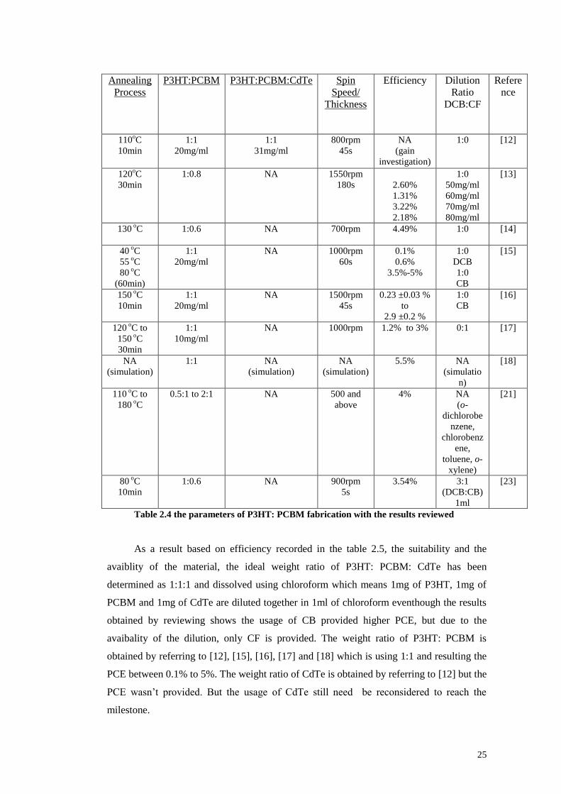
As a result based on efficiency recorded in the table 2.5, the suitability and the
avaiblity of the material, the ideal weight ratio of P3HT: PCBM: CdTe has been
determined as 1:1:1 and dissolved using chloroform which means 1mg of P3HT, 1mg of
PCBM and 1mg of CdTe are diluted together in 1ml of chloroform eventhough the results
obtained by reviewing shows the usage of CB provided higher PCE, but due to the
avaibality of the dilution, only CF is provided. The weight ratio of P3HT: PCBM is
obtained by referring to [12], [15], [16], [17] and [18] which is using 1:1 and resulting the
PCE between 0.1% to 5%. The weight ratio of CdTe is obtained by referring to [12] but the
PCE wasn’t provided. But the usage of CdTe still need be reconsidered to reach the
milestone.
26
The ideal annealing temperature obtained is between 80oC to 120
oC for 10 to 30
minutes for each annealing process. Most of the temperature shown in the table are quite
high and the heating durations are quite long too. Thus, to avoid from dissipating the
conductivity characteristic of each material, 90oC temperature and 5 minutes annealing
duration for each annealing process has been fixed.
2.3.3 PCDTBT: PCBM
The most recent electron donor polymeric material, PCDTBT, is currently being
deeply investigated in order to obtain the most efficient of polymer: fullerene solar cells.
Not only the performance, the morphology, architecture and lifetime of this device also
arebeing investigated. So, this material is still fresh and some information couldn’t be
obtained from rewiewing technical jurnals such as the usage of CdTe together with
PCDTBT:PCBM as active layer and the neither the refractive index. But, some important
characteristics are obtained as shown in the table 2.3.3a and the the chemical sctructure of
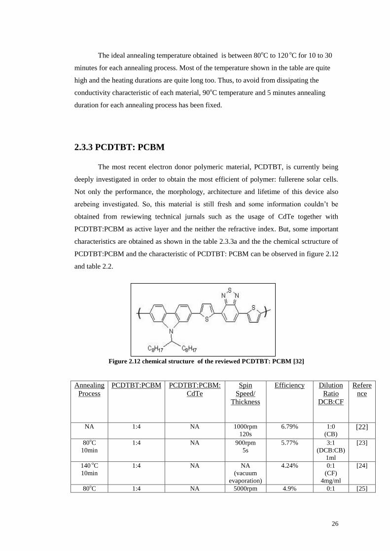
PCDTBT:PCBM and the characteristic of PCDTBT: PCBM can be observed in figure 2.12
and table 2.2.
Figure 2.12 chemical structure of the reviewed PCDTBT: PCBM [32]
Annealing
Process
PCDTBT:PCBM PCDTBT:PCBM:
CdTe
Spin
Speed/
Thickness
Efficiency Dilution
Ratio
DCB:CF
Refere
nce
NA
1:4 NA
1000rpm
120s 6.79% 1:0
(CB) [22]
80oC
10min
1:4 NA
900rpm
5s
5.77% 3:1
(DCB:CB)
1ml
[23]
140 oC
10min
1:4 NA NA
(vacuum
evaporation)
4.24% 0:1
(CF)
4mg/ml
[24]
80oC 1:4 NA 5000rpm 4.9% 0:1 [25]
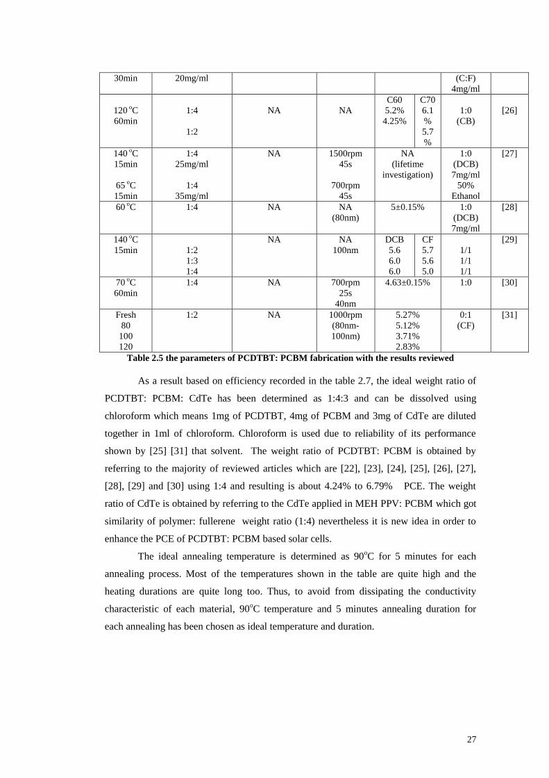
27
30min
20mg/ml (C:F)
4mg/ml
120 oC
60min
1:4
1:2
NA
NA
C60
5.2%
4.25%
C70
6.1
%
5.7
%
1:0
(CB)
[26]
140 oC
15min
65 oC
15min
1:4
25mg/ml
1:4
35mg/ml
NA 1500rpm
45s
700rpm
45s
NA
(lifetime
investigation)
1:0
(DCB)
7mg/ml
50%
Ethanol
[27]
60 oC
1:4 NA NA
(80nm)
5±0.15% 1:0
(DCB)
7mg/ml
[28]
140 oC
15min
1:2
1:3
1:4
NA NA
100nm
DCB
5.6
6.0
6.0
CF
5.7
5.6
5.0
1/1
1/1
1/1
[29]
70 oC
60min
1:4 NA 700rpm
25s
40nm
4.63±0.15% 1:0 [30]
Fresh
80
100
120
1:2 NA 1000rpm
(80nm-
100nm)
5.27%
5.12%
3.71%
2.83%
0:1
(CF)
[31]
Table 2.5 the parameters of PCDTBT: PCBM fabrication with the results reviewed
As a result based on efficiency recorded in the table 2.7, the ideal weight ratio of
PCDTBT: PCBM: CdTe has been determined as 1:4:3 and can be dissolved using
chloroform which means 1mg of PCDTBT, 4mg of PCBM and 3mg of CdTe are diluted
together in 1ml of chloroform. Chloroform is used due to reliability of its performance
shown by [25] [31] that solvent. The weight ratio of PCDTBT: PCBM is obtained by
referring to the majority of reviewed articles which are [22], [23], [24], [25], [26], [27],
[28], [29] and [30] using 1:4 and resulting is about 4.24% to 6.79% PCE. The weight
ratio of CdTe is obtained by referring to the CdTe applied in MEH PPV: PCBM which got
similarity of polymer: fullerene weight ratio (1:4) nevertheless it is new idea in order to
enhance the PCE of PCDTBT: PCBM based solar cells.
The ideal annealing temperature is determined as 90oC for 5 minutes for each
annealing process. Most of the temperatures shown in the table are quite high and the
heating durations are quite long too. Thus, to avoid from dissipating the conductivity
characteristic of each material, 90oC temperature and 5 minutes annealing duration for
each annealing has been chosen as ideal temperature and duration.
28
2.4 Safety Requirements
In order to avoid any unpleasant incident from happening in the laboratory, proper
ethics and protocol need to be followed. They are Safety First, Acid Safety and Solvents
Safety.
Safety First is more describing about the ethics and behaviour of the personnel
(people who use the laboratory) themselves. They must wear long pants, no shorts or
skirts, wear fully closed toe shoes and avoid wearing contact lens in clean room. They
must label every container used with this information; chemical, time and date, and their
name. Before entering the laboratory (or cleanroom), they should clean up after
themselves.Food or drink are forbidden in the lab. They also must know the exact position
or location of emergency shower, eye wash and calcium cream. Report any chemical spills
to technician or supervisor. If any accident happen, call the emergency number as soon as
possible.
Usually they will be exposed to the usage of acids in the etching process. Most of
the acids are corrosive, flammable and might be a minority type of them could be mutative.
A very proper way of handling must be taken. Always wear safety glasses and chemical
resistant gloves. Always Add Acid to water (AAA). Pour acids in slowly. Unwanted
reactions may occur if mixed incorrectly. Don’t inhale any fumes in the lab. Always use
chemicals under a fume hood.After mixing acid solutions make sure they are cooled to
room temperature before capping. This is to avoid pressure build up in the bottle. Make
sure acid bottles are always capped. Acids and solvents have to be disposed of in their
respective disposal bottle. If any acid is spilled on their person, rise thoroughly with large
quantities of water. Report the occurrence to the lab instructor immediately. When using
HF always use plastic. Don’t use any glass. The glass will be etched then unusable.[42]
In solvents preparation, this Solvent Safety is extremely important for the
personnel to follow. Most importantly in solvents handling, do not mix acids and solvents
together because by mixing them will cause highly explosive solutions or other unwanted
reaction. After done using the solvents, do not pour them down the sink. The Lab
instructor (technician) will show you the proper way to dispose of them. They go into the
solvent waste bottle if there is not a specific bottle for it. Always use solvents in a fume
hood. Most of the solvents fumes have some sort of toxic property. Don’t get solvents on
the skin. Most are readily absorbed through the skin and some are carcinogenic.
Photoresist contains these solvents so handle photoresist with the utmost care. In general
solvents are flammable, so be very careful around ignition sources. Do not allow solvent
fumes to come near an ignition source. Always wash gloves after handling solvents, so that
29
if the gloves come in contact with acids there in not chemical reaction. Don’t use the same
gloves for handling solvents and acids. The stains left on the glove might react too. For
more information about the safety in dilution process, referring to the material safety data
sheet (MSDS) is a must.[42]
2.5 Conclusion
Based on the comparison of all appropriate technique that can be used to deposit the
solvents on the substrate, it can be concluded that electro-deposition is the best technique
can be used. But the avaibality of the equipment also need to be considered. Thus, spin
coating is used due to the avaibality, lower cost and easier to be used. Eventhough the
theoretical calculation formula is covered in this chapter, but it’s not the purpose of
proving the thickness obtained by the experiment compared to the thickness evaluated
using a calculation. The characteristic of MEH PPV: PCBM, P3HT: PCBM and PCDTBT:
PCBM are recorded, compared and MEH PPV: PCBM is chose to be used as the active
layer in the experiment.
The main purpose of studying those 3 types of active layer is to investigate what
process involved, the parameter and finest tune, and the best PCE obtained. When the
required information is obtained, the variation and parameter can be set, the proper method
of producing the device can be arranged. It could save cost too regarding to the prevention
of buying inappropriate materials.
Besides that, by reviewing several articles regarding to the Safety Requirement in
the laboratory, a proper way of handling tools, suit required and hazardous of the material
can be determined. Thus, any accident at laboratory could be avoided.
30
Chapter 3 Methodology
3.1 Introduction
In order to fabricate the polymer:fullerene solar cells, the main method of processing
the layer has to be determined and the characteristic of the materials themselves need to be
recognized well so the proper methods could be arranged well. A lot of litereature has been
reviewed in order to obtain the methods and the material finest tunings with their power
conversion efficiencies obtained.
This fabrication is involving material preparation such as active layer dilutions
(solvent preparations), spin coating, cleaning, annealing, etching, results observation and
efficiencies calculation.
After obtaining all the required information, the table of conditions varied for the
solar cell is constructed to determine the amount of samples need to be fabricated.
Table 3.1 Predicted number of devices that required to be fabricated
Referring to the Table 3.1 a, it can be concluded that the amount of the samples need
to be fabricated are 16 samples. The varied conditions are the types of fullerene used
(whether using PC60BM or PC70BM) the additive of CdTe or without CdTe, and the spin
speeds of spin coating. The flow of fabrication process can be observed in Figure 3.1.
Polymer: Fullerene Solar Cells
MEH PPV
PC60BM PC70BM
No CdTe CdTe No CdTe CdTe
1000rpm 1000rpm 1000rpm 1000rpm
2000rpm 2000rpm 2000rpm 2000rpm
3000rpm 3000rpm 3000rpm 3000rpm
4000rpm 4000rpm 4000rpm 4000rpm
31
Figure 3.1 Device fabrication steps
PEDOT: PSS deposition
Substrate annealing
TiO2 Paste
ITO coated glass sandwiching
Start
Preparation of the Solvents based on the finest tuning
ITO etch
ITO coated glass cleaning and drying
Clean?
Yes
No
PEDOT: PSS etch
MEH PPV: PCBM deposition
Substrate annealing
MEH PPV: PCBM etch
Substrate annealing
UV-Vis Absorbance and I-V characteristic inspection
End
32
3.2 Preparation of the Solvents based on the finest tuning
3.2.1 MEH PPV:PCBM
The weight ratio of MEH PPV: PCBM: CdTe has been determined as 1:4:3 and
dissolved using chloroform which means 1mg of MEH PPV, 4mg of PCBM and 3mg of
CdTe are diluted together in 1ml of chloroform. This weight ratio is going to be used in the
experimental and is fixed. 20ul each drop. The PEDOT: PSS is already in the form of
chemical so it doesn’t require a dilution process.
The TiO2 is in form of powder so it requires to be diluted. 9ml of acid acetic nitric
is required to dissolve 6 gram of TiO2. The process need to be done little by little which
means 1ml is dropped into beaker filled with 6g of TiO2 at the same time the mixture is
grinded slowly but heavily pressed. This process is continuously done till the 9ml of acid
acetic nitric is finished. After that, the complete mixture need to be anneal on the hot plate
with 300oC for 10min to20min (until the colour is changed to brown and back to white).
3.3 Full Fabrication Process
First of all, a piece of ITO coated glass is cut to 100 samples with 2cm x 2cm unit
area. Then all the samples are cleaned using acetone or deconex which mean they are
dipped in a beaker filled with that solutions. After 20 to 30 minutes, all the glass substrates
are rinsed using DI water and dried using an air pump.
3/4 of the ITO layer which means 1.5cmx1.5cm unit area need to be etched. The
mixture of acid nitric and HCL with ratio 1:3 can be used for this process. The part to be
etched is dipped into a beaker filled with either one of those solution for 5min to 10min.
As the substrate is dipped, bubble will appear on the etched ITO surface and this
phenomenon stops when the ITO is totally etched. Then the glass substrate is cleaned using
DI water and dried using an air pump. This process is done for all the hundred substrate.
The figure 3.2 shows the cross section of the substrate.
Bottom glass Top glass
Figure 3.2
Glass
ITO
33
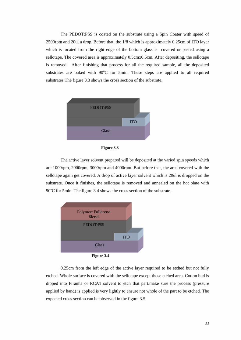
The PEDOT:PSS is coated on the substrate using a Spin Coater with speed of
2500rpm and 20ul a drop. Before that, the 1/8 which is approximately 0.25cm of ITO layer
which is located from the right edge of the bottom glass is covered or pasted using a
sellotape. The covered area is approximately 0.5cmx0.5cm. After depositing, the sellotape
is removed. After finishing that process for all the required sample, all the deposited
substrates are baked with 90oC for 5min. These steps are applied to all required
substrates.The figure 3.3 shows the cross section of the substrate.
Figure 3.3
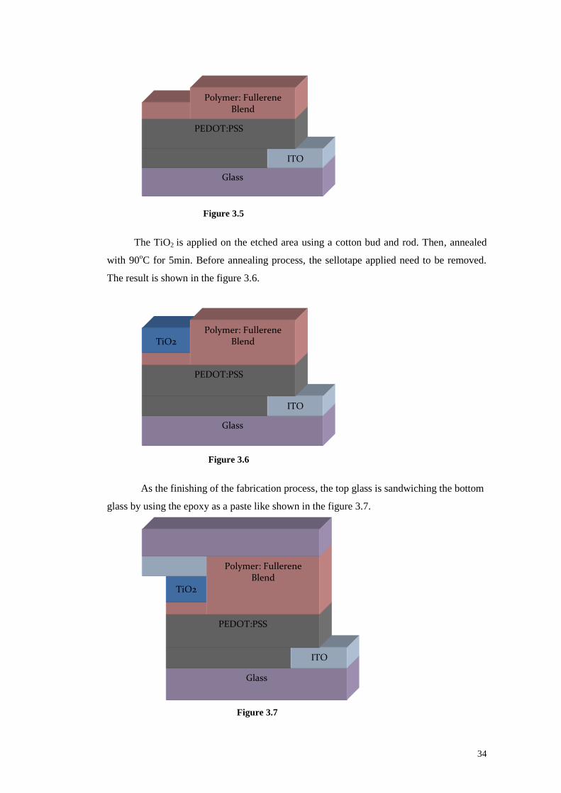
The active layer solvent prepared will be deposited at the varied spin speeds which
are 1000rpm, 2000rpm, 3000rpm and 4000rpm. But before that, the area covered with the
sellotape again get covered. A drop of active layer solvent which is 20ul is dropped on the
substrate. Once it finishes, the sellotape is removed and annealed on the hot plate with
90oC for 5min. The figure 3.4 shows the cross section of the substrate.
Figure 3.4
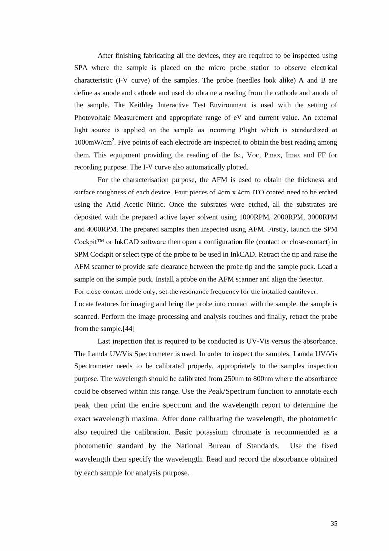
0.25cm from the left edge of the active layer required to be etched but not fully
etched. Whole surface is covered with the sellotape except those etched area. Cotton bud is
dipped into Piranha or RCA1 solvent to etch that part.make sure the process (pressure
applied by hand) is applied is very lightly to ensure not whole of the part to be etched. The
expected cross section can be observed in the figure 3.5.
Glass
ITO
PEDOT:PSS
Glass
ITO
PEDOT:PSS
Polymer: Fullerene Blend
34
Figure 3.5
The TiO2 is applied on the etched area using a cotton bud and rod. Then, annealed
with 90oC for 5min. Before annealing process, the sellotape applied need to be removed.
The result is shown in the figure 3.6.
Figure 3.6
As the finishing of the fabrication process, the top glass is sandwiching the bottom
glass by using the epoxy as a paste like shown in the figure 3.7.
Figure 3.7
Glass
ITO
PEDOT:PSS
Polymer: Fullerene Blend
Glass
ITO
PEDOT:PSS
TiO2 Polymer: Fullerene
Blend
Glass
ITO
PEDOT:PSS
TiO2
Polymer: Fullerene Blend
35
After finishing fabricating all the devices, they are required to be inspected using
SPA where the sample is placed on the micro probe station to observe electrical
characteristic (I-V curve) of the samples. The probe (needles look alike) A and B are
define as anode and cathode and used do obtaine a reading from the cathode and anode of
the sample. The Keithley Interactive Test Environment is used with the setting of
Photovoltaic Measurement and appropriate range of eV and current value. An external
light source is applied on the sample as incoming Plight which is standardized at
1000mW/cm2. Five points of each electrode are inspected to obtain the best reading among
them. This equipment providing the reading of the Isc, Voc, Pmax, Imax and FF for
recording purpose. The I-V curve also automatically plotted.
For the characterisation purpose, the AFM is used to obtain the thickness and
surface roughness of each device. Four pieces of 4cm x 4cm ITO coated need to be etched
using the Acid Acetic Nitric. Once the subsrates were etched, all the substrates are
deposited with the prepared active layer solvent using 1000RPM, 2000RPM, 3000RPM
and 4000RPM. The prepared samples then inspected using AFM. Firstly, launch the SPM
Cockpit™ or InkCAD software then open a configuration file (contact or close-contact) in
SPM Cockpit or select type of the probe to be used in InkCAD. Retract the tip and raise the
AFM scanner to provide safe clearance between the probe tip and the sample puck. Load a
sample on the sample puck. Install a probe on the AFM scanner and align the detector.
For close contact mode only, set the resonance frequency for the installed cantilever.
Locate features for imaging and bring the probe into contact with the sample. the sample is
scanned. Perform the image processing and analysis routines and finally, retract the probe
from the sample.[44]
Last inspection that is required to be conducted is UV-Vis versus the absorbance.
The Lamda UV/Vis Spectrometer is used. In order to inspect the samples, Lamda UV/Vis
Spectrometer needs to be calibrated properly, appropriately to the samples inspection
purpose. The wavelength should be calibrated from 250nm to 800nm where the absorbance
could be observed within this range. Use the Peak/Spectrum function to annotate each
peak, then print the entire spectrum and the wavelength report to determine the
exact wavelength maxima. After done calibrating the wavelength, the photometric
also required the calibration. Basic potassium chromate is recommended as a
photometric standard by the National Bureau of Standards. Use the fixed
wavelength then specify the wavelength. Read and record the absorbance obtained
by each sample for analysis purpose.
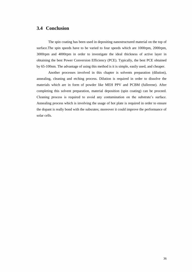
36
3.4 Conclusion
The spin coating has been used in depositing nanostructured material on the top of
surface.The spin speeds have to be varied to four speeds which are 1000rpm, 2000rpm,
3000rpm and 4000rpm in order to investigate the ideal thickness of active layer in
obtaining the best Power Conversion Efficiency (PCE). Typically, the best PCE obtained
by 65-100nm. The advantage of using this method is it is simple, easily used, and cheaper.
Another processes involved in this chapter is solvents preparation (dilution),
annealing, cleaning and etching process. Dilution is required in order to dissolve the
materials which are in form of powder like MEH PPV and PCBM (fullerene). After
completing this solvent preparation, material deposition (spin coating) can be proceed.
Cleaning process is required to avoid any contamination on the substrate’s surface.
Annealing process which is involving the usage of hot plate is required in order to ensure
the dopant is really bond with the subsrates; moreover it could improve the performance of
solar cells.
37
Chapter 4 Results and discussion
4.1 Introduction
After preparing all the samples, they are severals methods to do in inspecting the
device characteristic and performance. Basically this inspection purpose is about gathering
the behaviour information of each device.
Typically the informations obtained are the power max (Pmax), current max (Imax),
voltage max (Vmax), open circuit voltage (Voc), short circuit current (Isc) and fill factor
(FF). Pin or Plight is the illumination light applied on each device where the power is fixed
to 1000mW. Using this obtained information, the power conversion efficiency can be
evaluated by replacing the values in the formula below : [35]
(Im max)
( )
ax VFF
Isc Voc
( 4.1 )
( )FF Voc Isc
Pin
( 4.2 )
In the experiments conducted, there are several results obtained which are varied
based on the spin speeds, the usage and non-usage of carbon as counter electrode,and the
usage and non usage of CdTe as nano-scale interpenetrating network. The characterization
and the results of each device is recorded.
The instruments used in this section are Atomic Force Microscopy (AFM) which
is used to characterize the surface roughness and the thickness of coated active layer, UV-
Visible Spectroscopy which is used to analyse the absorbance and transmittance of the
polymer: fullerene layer, and Semiconductor Parametric Analyzer (SPA) which is used to
inspect the I-V curved and evaluation of power conversion efficiency (PCE) also
simbolized as η.
38
4.1.1 Characterisation
The characterisation is obtained via setting up the variation of the spin speed.
There are four spin speeds varied which is 1000rpm, 2000rpm, 3000rpm and 4000rpm.
This is to investigate how do the thickness and the morphology of the active layer affecting
the efficiency of the device.
Spin
Speeds
Thickness of
MEHPPV:PCBM
1:4
Surface Roughness
1000 RPM 40nm
2000 RPM 30nm
3000 RPM 20nm
4000 RPM 10nm
Table 4.1 Devices Characterisation
39
Table 4.1 shows that the differences of the thicknesses and the surface roughnesses
are obtained by using different spin speeds. For the lowest spin speed, coarsest surface was
obtained with the thickness is 40nm followed by 2000rpm with 30nm, 3000rpm with 20nm
and 4000rpm with 10nm and smoothest surface. The purpose of this characterization is to
relate the thickness obtained to the performance of each device.
4.1.2 Experimental results of UV-Visible λ evaluated based on the
spin speeds:
This experiment was conducted to observe the relation of the thickness of the
active layer with the absorption to the fixed value of the wavelength which is from 250nm
to 800nm. 250nm to 375nm is under UV spectrum, 375nm to 745nm is under Visible (Vis)
spectrum, and 745nm to 800nm is under Near Infra-Red (NIR) spectrum. This is shown in
the figure 4.1.
Figure 4.1 Electromagnetic Spectrum
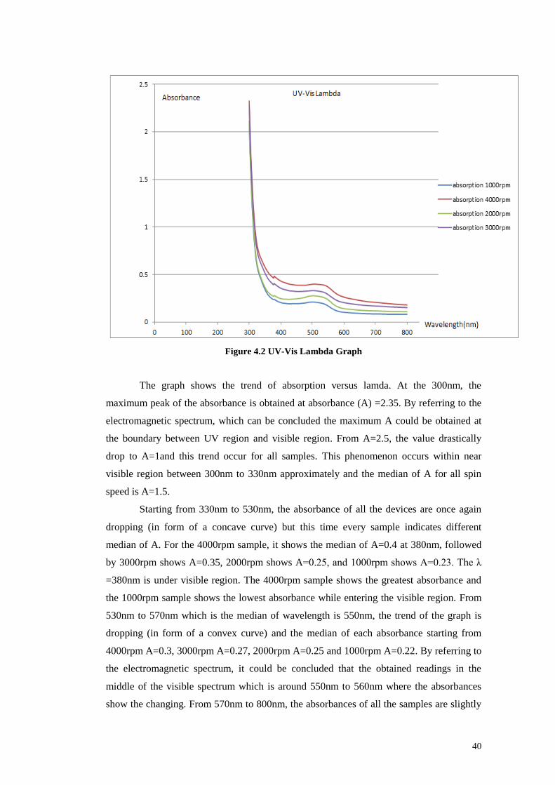
40
Figure 4.2 UV-Vis Lambda Graph
The graph shows the trend of absorption versus lamda. At the 300nm, the
maximum peak of the absorbance is obtained at absorbance (A) =2.35. By referring to the
electromagnetic spectrum, which can be concluded the maximum A could be obtained at
the boundary between UV region and visible region. From A=2.5, the value drastically
drop to A=1and this trend occur for all samples. This phenomenon occurs within near
visible region between 300nm to 330nm approximately and the median of A for all spin
speed is A=1.5.
Starting from 330nm to 530nm, the absorbance of all the devices are once again
dropping (in form of a concave curve) but this time every sample indicates different
median of A. For the 4000rpm sample, it shows the median of A=0.4 at 380nm, followed
by 3000rpm shows A=0.35, 2000rpm shows A=0.25, and 1000rpm shows A=0.23. The λ
=380nm is under visible region. The 4000rpm sample shows the greatest absorbance and
the 1000rpm sample shows the lowest absorbance while entering the visible region. From
530nm to 570nm which is the median of wavelength is 550nm, the trend of the graph is
dropping (in form of a convex curve) and the median of each absorbance starting from
4000rpm A=0.3, 3000rpm A=0.27, 2000rpm A=0.25 and 1000rpm A=0.22. By referring to
the electromagnetic spectrum, it could be concluded that the obtained readings in the
middle of the visible spectrum which is around 550nm to 560nm where the absorbances
show the changing. From 570nm to 800nm, the absorbances of all the samples are slightly
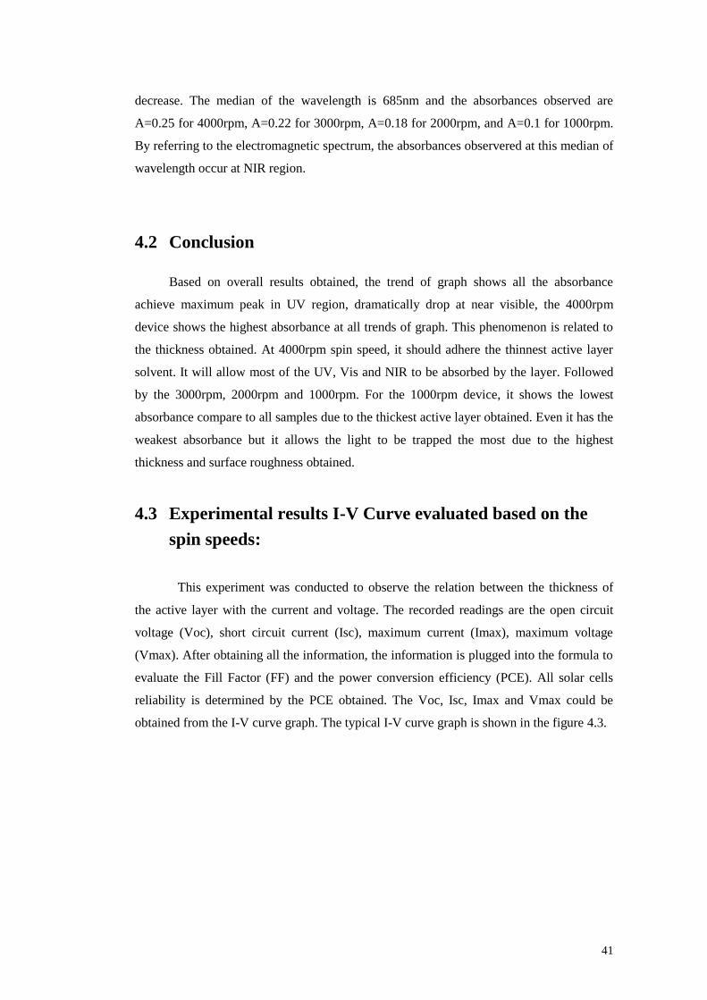
41
decrease. The median of the wavelength is 685nm and the absorbances observed are
A=0.25 for 4000rpm, A=0.22 for 3000rpm, A=0.18 for 2000rpm, and A=0.1 for 1000rpm.
By referring to the electromagnetic spectrum, the absorbances observered at this median of
wavelength occur at NIR region.
4.2 Conclusion
Based on overall results obtained, the trend of graph shows all the absorbance
achieve maximum peak in UV region, dramatically drop at near visible, the 4000rpm
device shows the highest absorbance at all trends of graph. This phenomenon is related to
the thickness obtained. At 4000rpm spin speed, it should adhere the thinnest active layer
solvent. It will allow most of the UV, Vis and NIR to be absorbed by the layer. Followed
by the 3000rpm, 2000rpm and 1000rpm. For the 1000rpm device, it shows the lowest
absorbance compare to all samples due to the thickest active layer obtained. Even it has the
weakest absorbance but it allows the light to be trapped the most due to the highest
thickness and surface roughness obtained.
4.3 Experimental results I-V Curve evaluated based on the
spin speeds:
This experiment was conducted to observe the relation between the thickness of
the active layer with the current and voltage. The recorded readings are the open circuit
voltage (Voc), short circuit current (Isc), maximum current (Imax), maximum voltage
(Vmax). After obtaining all the information, the information is plugged into the formula to
evaluate the Fill Factor (FF) and the power conversion efficiency (PCE). All solar cells
reliability is determined by the PCE obtained. The Voc, Isc, Imax and Vmax could be
obtained from the I-V curve graph. The typical I-V curve graph is shown in the figure 4.3.
C) Efficiency Measurement
FF = Fill factor Isc = Short circuit current Voc = Open Circuit Voltage Plight = Incident light power
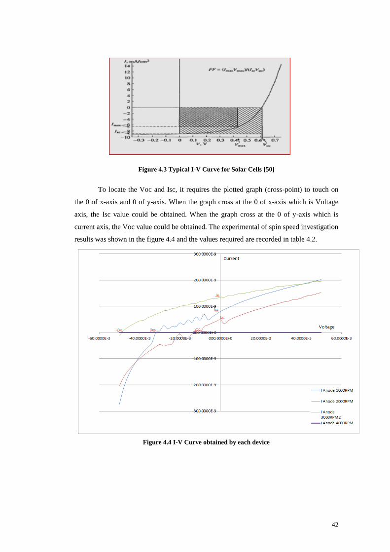
42
Figure 4.3 Typical I-V Curve for Solar Cells [50]
To locate the Voc and Isc, it requires the plotted graph (cross-point) to touch on
the 0 of x-axis and 0 of y-axis. When the graph cross at the 0 of x-axis which is Voltage
axis, the Isc value could be obtained. When the graph cross at the 0 of y-axis which is
current axis, the Voc value could be obtained. The experimental of spin speed investigation
results was shown in the figure 4.4 and the values required are recorded in table 4.2.
Figure 4.4 I-V Curve obtained by each device
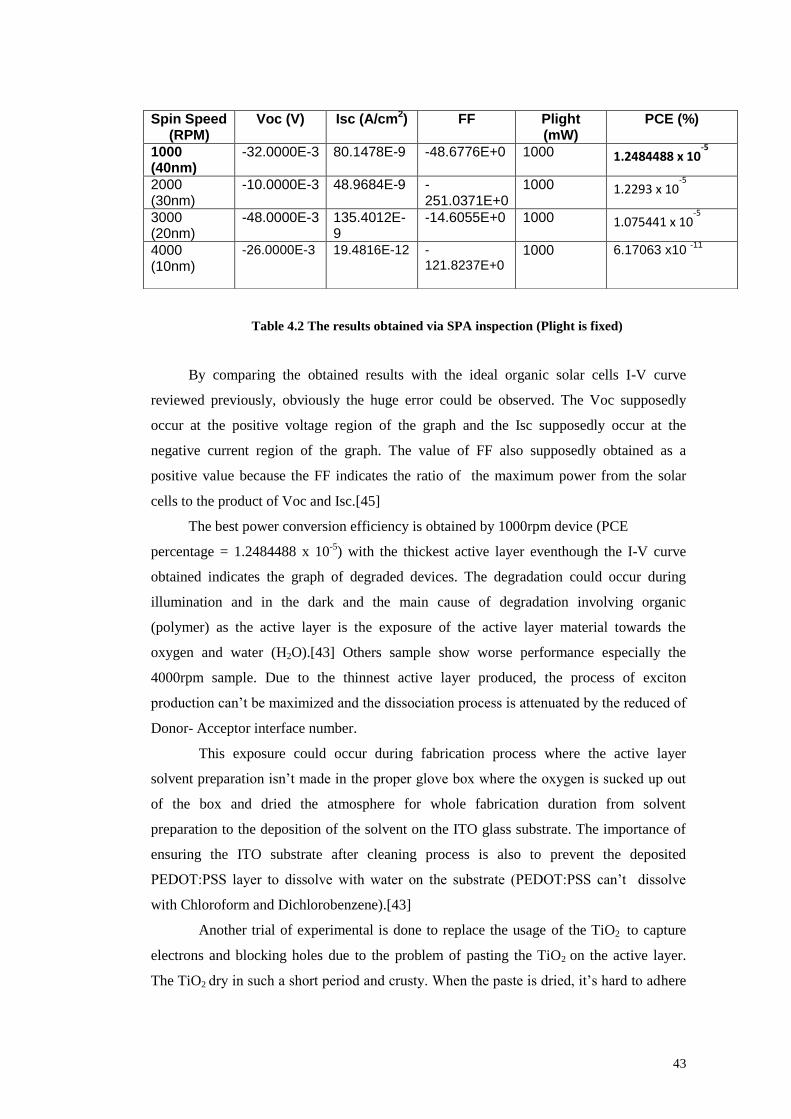
43
Table 4.2 The results obtained via SPA inspection (Plight is fixed)
By comparing the obtained results with the ideal organic solar cells I-V curve
reviewed previously, obviously the huge error could be observed. The Voc supposedly
occur at the positive voltage region of the graph and the Isc supposedly occur at the
negative current region of the graph. The value of FF also supposedly obtained as a
positive value because the FF indicates the ratio of the maximum power from the solar
cells to the product of Voc and Isc.[45]
The best power conversion efficiency is obtained by 1000rpm device (PCE
percentage = 1.2484488 x 10⁻⁵
) with the thickest active layer eventhough the I-V curve
obtained indicates the graph of degraded devices. The degradation could occur during
illumination and in the dark and the main cause of degradation involving organic
(polymer) as the active layer is the exposure of the active layer material towards the
oxygen and water (H2O).[43] Others sample show worse performance especially the
4000rpm sample. Due to the thinnest active layer produced, the process of exciton
production can’t be maximized and the dissociation process is attenuated by the reduced of
Donor- Acceptor interface number.
This exposure could occur during fabrication process where the active layer
solvent preparation isn’t made in the proper glove box where the oxygen is sucked up out
of the box and dried the atmosphere for whole fabrication duration from solvent
preparation to the deposition of the solvent on the ITO glass substrate. The importance of
ensuring the ITO substrate after cleaning process is also to prevent the deposited
PEDOT:PSS layer to dissolve with water on the substrate (PEDOT:PSS can’t dissolve
with Chloroform and Dichlorobenzene).[43]
Another trial of experimental is done to replace the usage of the TiO2 to capture
electrons and blocking holes due to the problem of pasting the TiO2 on the active layer.
The TiO2 dry in such a short period and crusty. When the paste is dried, it’s hard to adhere
Spin Speed (RPM)
Voc (V) Isc (A/cm2) FF Plight
(mW) PCE (%)
1000 (40nm)
-32.0000E-3 80.1478E-9 -48.6776E+0 1000 1.2484488 x 10⁻⁵
2000 (30nm)
-10.0000E-3 48.9684E-9 -251.0371E+0
1000 1.2293 x 10⁻⁵
3000 (20nm)
-48.0000E-3 135.4012E-9
-14.6055E+0 1000 1.075441 x 10⁻⁵
4000 (10nm)
-26.0000E-3
19.4816E-12
-121.8237E+0
1000 6.17063 x10 -11
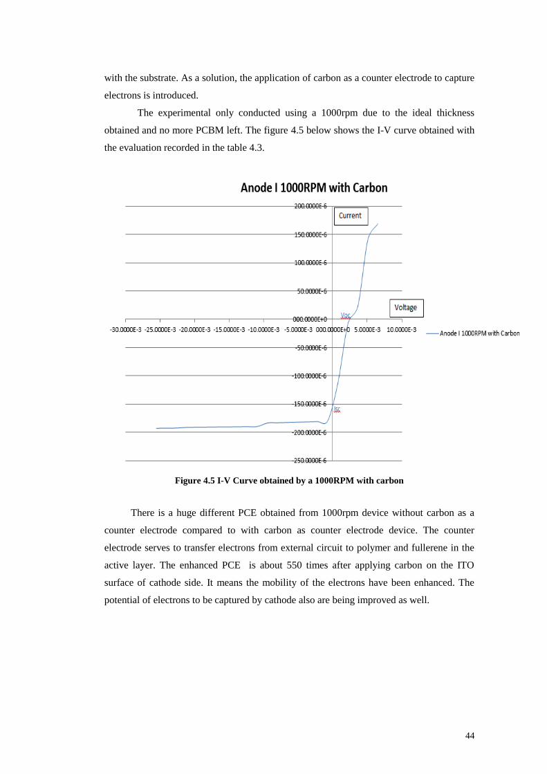
44
with the substrate. As a solution, the application of carbon as a counter electrode to capture
electrons is introduced.
The experimental only conducted using a 1000rpm due to the ideal thickness
obtained and no more PCBM left. The figure 4.5 below shows the I-V curve obtained with
the evaluation recorded in the table 4.3.
Figure 4.5 I-V Curve obtained by a 1000RPM with carbon
There is a huge different PCE obtained from 1000rpm device without carbon as a
counter electrode compared to with carbon as counter electrode device. The counter
electrode serves to transfer electrons from external circuit to polymer and fullerene in the
active layer. The enhanced PCE is about 550 times after applying carbon on the ITO
surface of cathode side. It means the mobility of the electrons have been enhanced. The
potential of electrons to be captured by cathode also are being improved as well.
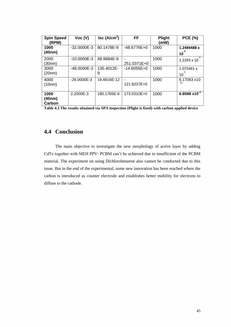
45
Table 4.3 The results obtained via SPA inspection (Plight is fixed) with carbon applied device
4.4 Conclusion
The main objective to investigate the new morphology of active layer by adding
CdTe together with MEH PPV: PCBM can’t be achieved due to insufficient of the PCBM
material. The experiment on using Dichlorobenzene also cannot be conducted due to this
issue. But in the end of the experimental, some new innovation has been reached where the
carbon is introduced as counter electrode and establishes better mobility for electrons to
diffuse to the cathode.
Spin Speed (RPM)
Voc (V) Isc (A/cm2) FF Plight
(mW) PCE (%)
1000 (40nm)
-32.0000E-3 80.1478E-9 -48.6776E+0 1000 1.2484488 x
10-5
2000 (30nm)
-10.0000E-3 48.9684E-9 -251.0371E+0
1000 1.2293 x 10⁻⁵
3000 (20nm)
-48.0000E-3 135.4012E-9
-14.6055E+0 1000 1.075441 x
10-5
4000 (10nm)
-26.0000E-3
19.4816E-12
-121.8237E+0
1000 6.17063 x10 -11
1000 (40nm) Carbon
2.2000E-3
180.1765E-6
173.0310E+0
1000 6.8588 x10⁻³
46
Chapter 5 Business plan
5.1 Introduction
Due to the appropriate climate in our country which is summer for the whole year, it
turns to be a huge advantage to use a green, renewable energy harvesting method. It will
become good replacement the Gas usage to generate electricity. Regarding of a lot
development and approaching in order to increase the efficiency with lower cost material,
the price is decreased. This is a positive opportunity to trigger a huge development in
producing solar cell including organic solar cell which costs the cheapest among the
photovoltaic devices.
The latest news is Panasonic Malaysia Sdn Bhd is launching new solar
manufacturing base in Kulim Hitech Kedah, predicted to start operation this December
2012. Panasonic ready to spend RM1.82 billion to develop this facility which can produce
approximately 300MW a year.
5.2 Market analysis including effect on society and
environment
Nowadays, peoples realize the importance of having a green, environmental
unharmful energy sources. The global warming are the biggest issues and always being
discuss among peoples. The technology and the lifestyles are enhanced from days to days.
All the technology also requires energy source.
The globalization is involving the whole world and all the countries won’t be left
behind. If the hydro power plant and gas power plant are built in huge number, many trees,
jungle and hills need to be cut down due the space required in building those power plants.
The trees are contributing the most in air circulation and stabilize the atmosphere. If the
trees are cutdown, the atmosphere wont be stabil no more yet causing to the global
warming.
47
Worse, this phenomenon could lead to the big flood when the trees are gone and the
hills are shrinked, there are no more rain fall filtering. The rains will directly fall to the soil
without being scattered by any filter and the soil cant manage to absorb all the water inside
at the very same time. This phenomenon will cause a big flood.
Thus, the invention and application of solar cells is reasonable for society especially
the organic solar cells. Inside the earth is rich with polymer materials and yet not all of are
investigated. The transparency of the polymer solar cells make it suitable to be installed as
a window of the house and vehicle. The flexibility of the plastic substrates make it
appropriate to be mounted on the clothes and even the umbrella. So a lot of space can be
saved. This advantages make it suitable to earn profit as much as possible in the marketing.
But, due to it’s low power conversion efficiency and short lifetime (easily degrade when
exposed to the water), a lot of effort to investigate and proper solutions are required to
ensure the marketing profit can be achieved.
The previous solar cells was introduced before the organic solar cells which is the
inorganic solar cells like silicon solar cells is providing splendid in power conversion
efficiency, the strong reliability against the outdoor weather, and longer lifetime. The
material used as a main substrate which is the sand is easily obtained everywhere and
easily processed too. But the capital cost for whole process is bigger compared to the
organic solar cells. It requires more equipment, solvents, dopants, longer fabrication
duration, and the processes are even more complex. The substrates also have heavier
weight and solid form; make it appropriate to be mounted on the roof or on the stand only.
5.3 Business structure
In order to become a good entrepreneur, several characteristic of successful
entrepreneur needs to be practiced. One of them are the entrepreneur should has passion
for the business; means the business require full commitment and full desire. The
entrenpreneur also need to focus on customer’s needs and demand. This is important to
avoid producing some wasting products and too risky to obtain customers. The business
won’t succeed if the product can’t brings benefit. In experiments of innovating the
product’s stage, failure is first step to success for tenacity entrepreneurs. Tenacity is
important because it show a potential customer the commitment of the entrepreneur about
his or her new products and services. To enhance or repair the error of the product, a
proper execution intelligence is required. It is important in order to analyse the opportunity
or troubleshooting to overcome the error thus enhancing the product performance.
48
Innovation is also important element in entrepreneurship, which can be defined by
a combination of the vision to create a good idea and the perseverance and dedication to
remain with the concept through implementation. They are four types of innovations which
are invention, extension, duplication, and synthesis. The invention innovation means the
product is totally new product, new service and using new processing method. The
extension innovation means the new use or different application of an already existing
product, service, or process. The duplication innovation means the creative replication of
an existing concept. The synthesis innovation means the combination of existing concepts
and factors into a new formulation or use.
To sustain the development of this polymer: fullerene solar cells, it requires bigger
material cost due to higher cost for the active layer conductive polymer powder like P3HT
and PCDTBT. The cooperation from outsiders or public also might needed to contribute a
share in developing and experimenting the new outcome of a new device.
5.4 Costing
The total estimated cost for this project consisted by several group of costing. They
are capital cost, operational cost, and material cost.
5.4.1 Capital cost
The capital cost is the cost estimated for starting the whole project such as the cost
for building the laborotary, protocol dress like bunny suit, glove, mask, safety shoes, and
the handling tools such as a tweeser, beaker and the equipments.
The proper laboratory will cost about RM200 to RM400 million including all the
facility like air circulation system (for ensuring the cleanliness and the best temperature of
the laboratory for proceeding any fabrication process), piping, 3 phase electrical wiring
installation with proper busbar and distribution board, and the suitable furniture like tables,
chairs and lockers.
To start fabricating the device, proper dresses are required due to the safety of the
personnel and the cleanliness of the device. The proper dress is including the coat or bunny
suit, mask, safety shoes, the latex glove or the thick glove (for handling high temperature
or high corrosive chemical), and of course, proper hand tools are also required to handle
the substrates or samples and chemicals like tweeser, beaker and etc. The estimated cost
for all of this items are approximately RM20k or below.
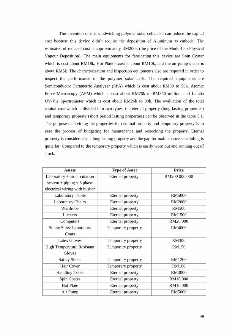
49
The invention of this sandwiching-polymer solar cells also can reduce the capital
cost because this device didn’t require the deposition of Aluminum as cathode. The
estimated of reduced cost is approximately RM200k (the price of the Modu-Lab Physical
Vapour Deposition). The main equipments for fabricating this device are Spin Coater
which is cost about RM18k, Hot Plate’s cost is about RM10k, and the air pump’s cost is
about RM5k. The characterization and inspection equipments also are required in order to
inspect the performance of the polymer solar cells. The required equipments are
Semiconductor Parametric Analyzer (SPA) which is cost about RM30 to 50k, Atomic
Force Microscopy (AFM) which is cost about RM70k to RM350 million, and Lamda
UV/Vis Spectrometer which is cost about RM26k to 30k. The evaluation of the total
capital cost which is divided into two types; the eternal property (long lasting properties)
and temporary property (short period lasting properties) can be observed in the table 5.1.
The purpose of dividing the properties into eternal property and temporary property is to
ease the process of budgeting for maintenance and restocking the property. Eternal
property is considered as a long lasting property and the gap for maintenance scheduling is
quite far. Compared to the temporary property which is easily worn out and running out of
stock.
Assets Type of Asset Price
Laboratory + air circulation
system + piping + 3 phase
electrical wiring with busbar
Eternal property RM200 000 000
Laboratory Tables Eternal property RM5000
Laboratory Chairs Eternal property RM2000
Wardrobe Eternal property RM500
Lockers Eternal property RM1500
Computers Eternal property RM20 000
Bunny Suits/ Laboratory
Coats
Temporary property RM4000
Latex Gloves Temporary property RM300
High Temperature Resistant
Gloves
Temporary property RM150
Safety Shoes Temporary property RM1200
Hair Cover Temporary property RM100
Handling Tools Eternal property RM3000
Spin Coater Eternal property RM18 000
Hot Plate Eternal property RM10 000
Air Pump Eternal property RM5000
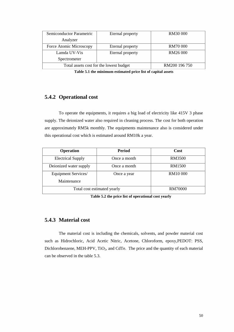
50
Table 5.1 the minimum estimated price list of capital assets
5.4.2 Operational cost
To operate the equipments, it requires a big load of electricity like 415V 3 phase
supply. The deionized water also required in cleaning process. The cost for both operation
are approximately RM5k monthly. The equipments maintenance also is considered under
this operational cost which is estimated around RM10k a year.
Operation Period Cost
Electrical Supply Once a month RM3500
Deionized water supply Once a month RM1500
Equipment Services/
Maintenance
Once a year RM10 000
Total cost estimated yearly RM70000
Table 5.2 the price list of operational cost yearly
5.4.3 Material cost
The material cost is including the chemicals, solvents, and powder material cost
such as Hidrochloric, Acid Acetic Nitric, Acetone, Chloroform, epoxy,PEDOT: PSS,
Dichlorobenzene, MEH-PPV, TiO2, and CdTe. The price and the quantity of each material
can be observed in the table 5.3.
Semiconductor Parametric
Analyzer
Eternal property RM30 000
Force Atomic Microscopy Eternal property RM70 000
Lamda UV-Vis
Spectrometer
Eternal property RM26 000
Total assets cost for the lowest budget RM200 196 750
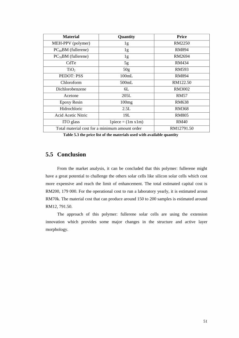
51
Table 5.3 the price list of the materials used with available quantity
5.5 Conclusion
From the market analysis, it can be concluded that this polymer: fullerene might
have a great potential to challenge the others solar cells like silicon solar cells which cost
more expensive and reach the limit of enhancement. The total estimated capital cost is
RM200, 179 000. For the operational cost to run a laboratory yearly, it is estimated aroun
RM70k. The material cost that can produce around 150 to 200 samples is estimated around
RM12, 791.50.
The approach of this polymer: fullerene solar cells are using the extension
innovation which provides some major changes in the structure and active layer
morphology.
Material Quantity Price
MEH-PPV (polymer) 1g RM2250
PC60BM (fullerene) 1g RM894
PC70BM (fullerene) 1g RM2694
CdTe 5g RM434
TiO2 50g RM593
PEDOT: PSS 100mL RM894
Chloroform 500mL RM122.50
Dichlorobenzene 6L RM3002
Acetone 205L RM57
Epoxy Resin 100mg RM638
Hidrochloric 2.5L RM368
Acid Acetic Nitric 19L RM805
ITO glass 1piece = (1m x1m) RM40
Total material cost for a minimum amount order RM12791.50
52
Chapter 6 Conclusion and future
work
6.1 Conclusion
In the first chapter, the history and the development of inorganic and organic solar
cells are studied to get the image and basic working principle of solar cells. The purpose of
investigation is to understand the mechanism of each process in order to convert photon
(sun light) to charge carrier (electrons holes pair) and dissociated to the external circuit or
load. The target was achieved and chapter 2 was proceeded to get some idea on structuring
the device.
A lot of literatures were reviewed in order to find the finest tune of solvents in term
of weight ratio, the appropriate dilutions, the morphology of the active layer, the ideal
temperature for annealing processes with time duration, the ideal of spin speed for
depositing the PEDOT: PSS layer with time duration, the suitable solutions for cleaning
purpose, the deposition methods, laboratory protocols and Material Safety Data Sheet
(MSDS). Not only MEH PPV: PCBM solar cells is reviewed, but the P3HT: PCBM and
PCDTBT: PCBM solar cells as well. This is because the reviewed information can be used
for any further future work. Once all the parameter is studied, the methodology of
fabricating the device can be engineered and run card can be prepared.
After obtaining the information on the device itself and the image of the device
structure, the main process is decided by using spin coating to deposit the solvents on the
substrate. The spin speeds are varied to four spin speed which are 1000rpm, 2000rpm,
3000rpm, and 4000rpm in order to investigate the ideal spin speed need to be used to get
the ideal thickness of the active layer. The spin speed for depositing the PEDOT:PSS layer
is fixed to 2500rpm for all devices due to its ideal spin speed investigated by reviewing the
jurnal. The temperature for annealing purpose is set to 90°C for 5. The required etching
solvent also is identified.
After done fabricating the devices of 1000rpm, 2000rpm, 3000rpm, and 4000rpm,
those devices were inspected using UV/Vis Spectroscopy, Atomic Force Microscopy and
Semiconductor Parametric Analyzer to analyse UV/ Visible spectrum with the absorbance,
the surface roughness with the thickness of each active layer, and to analyse and evaluate
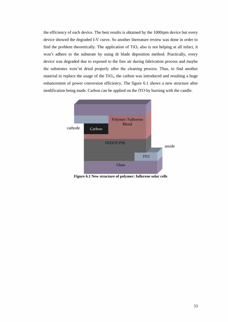
53
the efficiency of each device. The best results is obtained by the 1000rpm device but every
device showed the degraded I-V curve. So another litereature review was done in order to
find the problem theoretically. The application of TiO2 also is not helping at all infact, it
won’t adhere to the substrate by using dr blade deposition method. Practically, every
device was degraded due to exposed to the free air during fabrication process and maybe
the substrates were’nt dried properly after the cleaning process. Thus, to find another
material to replace the usage of the TiO2, the carbon was introduced and resulting a huge
enhancement of power conversion efficiency. The figure 6.1 shows a new structure after
modification being made. Carbon can be applied on the ITO by burning with the candle.
cathode
anode
Figure 6.1 New structure of polymer: fullerene solar cells
Glass
ITO
PEDOT:PSS
Carbon
Polymer: Fullerene Blend
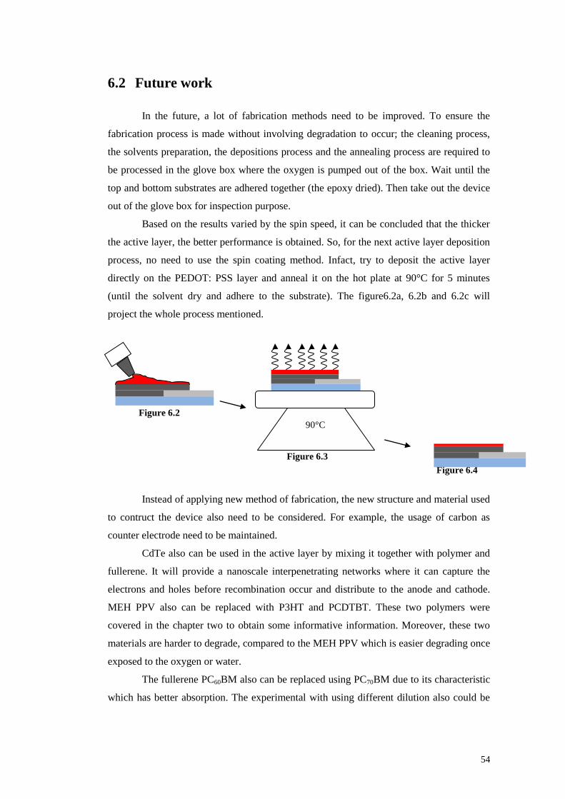
54
6.2 Future work
In the future, a lot of fabrication methods need to be improved. To ensure the
fabrication process is made without involving degradation to occur; the cleaning process,
the solvents preparation, the depositions process and the annealing process are required to
be processed in the glove box where the oxygen is pumped out of the box. Wait until the
top and bottom substrates are adhered together (the epoxy dried). Then take out the device
out of the glove box for inspection purpose.
Based on the results varied by the spin speed, it can be concluded that the thicker
the active layer, the better performance is obtained. So, for the next active layer deposition
process, no need to use the spin coating method. Infact, try to deposit the active layer
directly on the PEDOT: PSS layer and anneal it on the hot plate at 90°C for 5 minutes
(until the solvent dry and adhere to the substrate). The figure6.2a, 6.2b and 6.2c will
project the whole process mentioned.
Figure 6.2
Figure 6.3
Figure 6.4
Instead of applying new method of fabrication, the new structure and material used
to contruct the device also need to be considered. For example, the usage of carbon as
counter electrode need to be maintained.
CdTe also can be used in the active layer by mixing it together with polymer and
fullerene. It will provide a nanoscale interpenetrating networks where it can capture the
electrons and holes before recombination occur and distribute to the anode and cathode.
MEH PPV also can be replaced with P3HT and PCDTBT. These two polymers were
covered in the chapter two to obtain some informative information. Moreover, these two
materials are harder to degrade, compared to the MEH PPV which is easier degrading once
exposed to the oxygen or water.
The fullerene PC60BM also can be replaced using PC70BM due to its characteristic
which has better absorption. The experimental with using different dilution also could be
90°C

55
conducted to observe each potential of dilution to contribute to the performance of each
device.
The dichlorobenzene (DCB), tolune, and chloroform can be used to dissolve each
polymer: fullererne material. The dilution can be used as a stand alone dilution or mix. For
a mixed dilution, it can be 1: 1 weight ratio of DCB and CF.

56
List of publications
Papers: -
Exhibition: Final Year Project Expo (FYPEX) held by School Of
Microelectronic (SoME) UniMAP on 13 March 2013 (Winning a
Bronze Medal)
Conferences attended: -
57
References
1. K.Inpor, S.Rabaenko, P. Boonchan, C. Junin, C. Euvananont, S. Sahasithiwat, P.
Limthongkul, C. Sae-Kung, P. Sichanugrist and C. Thanachayanont, “Bulk
Heterojunction MEH-PPV:TiO2 Porous Structured Solar Cell” 12120 Pathumthani
Thailand.
2. Quynh Nhu Nguyen Truong, Nguyen Tam Nguyen Truong, Chinho Park and Jae
Hak Jung. “Study of MEH-PPV:PCBM active layer morphology and its
application for hybrid solar cells performance”, 712-749 Gyeongsan, Republic of
Korea, March 2011.
3. S. Alem, T. Chu, C. Tse, Salem Wakim, J. Lu, R. Movileanu, Y.Tao, F. Belanger,
D. Desilets, S. Beaupre, M. Leclerc, S. Rodman, D. Waller, R. Gaudiana. “Effect
of mixed solvents on PCDTBT:PC70BM based solar cells”, MA 01852, USA,
2011.
4. Salima Alem, Remi de Bettignies, and Jean-Michel Nunzi. “Efficient polymer-
based interpenetrated network photovoltaic cells”, 49045 Angers, France, March
2004.
5. DavidDuche , PhilippeTorchio, Ludovic Escoubas, Florent Monestier, Jean-
Jacques Simon, Franc-ois Flory, Ge´ rardMathian. “Improving light absorption in
organic solar cells by plasmonic contribution”, 13451 Marseille Cedex 20, France.
February 2009.
6. Liu Xiao-Dong, Zhao Su-Ling, Xu Zheng, Zhang Fu-Jun, Zhang Tian-Hui, Gong
Wei, Yan Guang, Kong Chao, Wang Yong-Sheng, and Xu Xu-Rong.
“Performance improvement of MEH-PPV:PCBM solar cells using bathocuproine
and bathophenanthroline as the buffer layers”, Beijing 100044, China. January
2011.
7. Lili Xue, LeijingLiu, QiangGao, ShanpengWen, JiatingHe, WenjingTian. “Planar-
diffused photovoltaic device based on the MEH-PPV/PCBM system prepared by
solution process”, Changchun 130012, PR China. December2008.
8. Elizabeth Alice Thomsen. “Characterisation Of Materials For Organic
Photovoltaics”, University of St. Andrews. 2008.
9. Sandeep Kumar and Thomas Nann. “First solar cells based on CdTe
nanoparticle/MEH-PPV composites”,Freiburg D-79104, Germany. April 2004.
58
10. Sheila G. Bailey Glem, Jerry D. Harris, Aloysius E Hepp Glem. “Thin-Film
Organic-Based Solar Cells for Space Power”, Cleveland, Ohio. August 2002.
11. Riski Titian Ginting, Chi Chin Yap, Muhammad Yahaya and Muhamad Mat
Salleh. “MEH-PPV: PCBM Solution Concentration Dependence of Inverted Type
Organic Solar Cells Based on Eosin-Y-coated ZnO Nanorod Arrays”, Selangor,
Malaysia.
12. Hsiang-Yu Chen, Michael K. F. Lo, Guanwen Yang, Harold G. Monbouquette,
and Yang Yang, “Nanoparticle-assisted High Photoconductive Gain in Composites
of Polymer and Fullerene”, Macmillan Publishers Limited, 2008.
13. O. Ourida et al. / SATRESET, Vol. 1, No. 3, pp. 90-92, September 2011
14. Transactions On Electrical And Electronic Materials Vol. 13, No. 2, pp. 98-101,
April 25, 2012
15. Gang Li, Vishal Shrotriya, Yan Yao, Jinsong Huang and Yang Yang;
“Manipulating regioregular poly(3-hexylthiophene) : [6,6]-phenyl-C61-butyric
acid methyl ester blends—route towards high efficiency polymer solar cells”,
Journal of Materials Chemistry, 11th June 2007.
16. Jenna deBoisblanc, Synthesis and Characterization of P3HT:PCBM Organic Solar
Cells, Senior Thesis, May 2010.
17. Giovanni Fanchini, Steve Miller and Manish Chhowalla, In situ
photoluminescence and Raman study of nanoscale morphological changes in
organic photovoltaics during solvent vapor annealing.
18. Young Min Nam, June Huh and Won Ho Jo; Optimization of thickness and
morphology of active layer for high performance of bulk-heterojunction organic
solar cells, Solar Energy Materials & Solar Cells 94 1118–1124, 2010
19. Kaloian Koynov, Ayi Bahtiar, Taek Ahn, and Christoph Bubeck; “Molecular
weight dependence of birefringence of thin films of the
conjugated polymer poly.2-methoxy-5-.28-ethyl-hexyloxy.-1,
4-phenylenevinylene”, Applied Physics Letters Volume 84, Number 19, 10 MAY
2004.
20. Nabok, Alexei “Organic and Inorganic nanostructures” Artech House MEMS
series, 2005.
21. Sigma-Aldrich, “Poly (3-hexylthiophene-2,5-diyl)”, Product Information.
22. Zhicai He , Chengmei Zhong , Xun Huang , Wai-Yeung Wong , Hongbin Wu ,
59
Liwei Chen , Shijian Su , and Yong Cao, “Simultaneous Enhancement of Open-
Circuit Voltage, Short-Circuit Current Density, and Fill Factor in Polymer Solar
Cells”, Adv. Mater. 23, 4636–4643, 2011.
23. Dong Hwan Wang, Do Youb Kim, Kyeong Woo Choi, Jung Hwa Seo, Sang Hyuk
Im, Jong Hyeok Park,O Ok Park, and Alan J. Heeger, “Enhancement of Donor–
Acceptor Polymer Bulk Heterojunction Solar Cell Power Conversion Efficiencies
by Addition of Au Nanoparticles”, Angew. Chem. Int. Ed. , 50, 5519 –5523, 2011.
24. Bo Wu, Than Zaw Oo, Xianglin Li, Xinfeng Liu, Xiangyang Wu, Edwin Kok Lee
Yeow, Hong Jin Fan, Nripan Mathews and Tze Chien Sum, “Efficiency
Enhancement in Bulk-Heterojunction Solar Cells Integrated with Large-Area Ag
Nanotriangle Arrays”, The Journal of Physical Chemistry C, 2012.
25. http://www.ossila.com/datasheets/Ossila_PCDTBT_data_sheet_v2.pdf
26. Ta-Ya Chu, Salima Alem, Pierre G. Verly, Salem Wakim and Jianping Lu,
“Highly efficient polycarbazole-based Organic Photovoltaic Devices”, Appl. Phys.
Lett. 95, 063304,2009.
27. Craig H. Peters, I. T. Sachs-Quintana, William R. Mateker, Thomas Heumueller,
Jonathan Rivnay, Rodigo Noriega, Zach M. Beiley, Eric T. Hoke, Alberto Salleo,
and Michael D. McGehee, “ The Mechanism of Burn-in Loss in a High Efficiency
Polymer Solar Cell”, Adv. Mater. 24, 663–668, 2012.
28. Craig H. Peters, I. T. Sachs-Quintana, John P. Kastrop, Serge Beaupre, Mario
Leclec, and Michael D. McGehee, “High Efficiency Polymer Solar Cell with Long
Operating Lifetimes”, Adv. Mater,1,491-494, 2011.
29. S. Alem, Ta-Ya Chu, Shing C. Tse, S. Wakim, Jianping Lu, R. Movileanu, Ye
Tao, F. Belanger, D. Desilets, S. Beaupre, M. Leclrec and Sheila Rodman, “Effect
of mixed solvents on PCDTBT:PC70BM based solar cells”, Organic Electronics
12, 1788-1793, 2011.
30. Abd.Rashid b. Mohd Yusoff, “Inverted Organic Solar Cells with TiOx cathode and
Graphene Oxide anode buffer layers” Solar Energy Materials & Solar Cells 109
63–69, 2013.
31. Yang Shao-Peng, Kong Wei-Guang, Liu Bo-Ya, Zheng Wen-Yao, Li Bao-Min,
Liu Xian-Hao and Fu Guang-Sheng, “Highly Efficient PCDTBT:PC71 BM Based
Photovoltaic Devices without Thermal Annealing Treatment”, CHIN. PHYS.
LETT. Vol. 28, No. 12 128401, 2011.
32. Shizuyasu Ochiai, Masaki Uchiyama, and Santhakumar Kannappan “Evaluation of
the Performance of an Organic Thin Film Solar Cell Prepared Using the Active
Layer of Poly[[9-(1-octylnonyl)-9H-carbazole-2.7-diyl]-2.5-thiophenediyl-2.1.3-
60
benzothiadiazole-4.7-Diyl-2.5-thiophenediyl]/[6,6]-Phenyl C71 Butyric Acid
Methyl Ester Composite Thin Film” Department of Electrical Eng., Aichi Institute
of Technology, 1247 Yakusa, Toyota 470-0392, Japan October 31, 2011.
33. Organic Solar Cell, Universita Degli Studi Di Padova.
34. “Recent Organic Solar Cell Technology & Market Forecast” (2010~2015) 2nd
Edition Solar&Energy Co., Ltd. April. 2011.
35. Marcos Soldera, Kurt Taretto, and Thomas Kirchartz “Comparison of device
models for organic solar cells: Band-to-band vs. tail states recombination”
Departamento de Electrotecnia, Universidad Nacional del Comahue, Buenos Aires
1400, 8300 Neuque´n, Argentina, Department of Physics, ImperialCollege
London, South Kensington SW7 2AZ, UK 4 May 2011.
36. Kangmin Wu “Advanced Materials and Fabrication Methods for Organic Solar
Cells” Thesis, Mc Master University ,11 January 2010.
37. Laxman Anishetty ,“Schottky behavior of organic solar cells with different
cathode deposition methods” thesis, Master of Science Degree in Electrical
Engineering.
38. Yen-Ju Cheng, Sheng-Hsiung Yang, and Chain-Shu Hsu ,“Synthesis of
Conjugated Polymers for Organic Solar Cell Applications”,Department of Applied
Chemistry, National Chiao Tung University, 1001 Ta Hsueh Road, Hsin-Chu
30049, Taiwan May 7, 2009.
39. “Photolitography”, Fabrication Fundamental EMT261 SoME, UniMAP 2010
40. Kang-Shyang Liao, Soniya D. Yambem , Amrita Haldar , Nigel J. Alley and
Seamus A. Curran, “Designs and Architectures for the Next Generation of Organic
Solar Cells”, Institute for NanoEnergy, Department of Physics, University of
Houston, Houston, TX 77004, USA ,School of Physical Sciences, Dublin City
University, Glasnevin, Dublin 9, Ireland March, 2010.
41. Zhen Guo and Li Tan, “Fundamentals and Applications of Nanomaterials”, Artech
House, 2009.
42. Dr. Todd J. Kaiser, “Introduction, Safety and Protocol”, EE580 Solar Cell Basics
for Teachers; Montana State University: Solar Cells.
43. Frederik C. Krebs, Kion Norrman, J. Mikkel, "Stability/ degradation of Polymer
Solar Cells", National Laboratory for Sustainable Energy, Technical University of
Denmark, ScienceDirect, 2008.
44. http://www.stevens.edu/lmsi/Files/How_to_use_AFM_simple_instruction.pdf
45. http://pveducation.org/pvcdrom/solar-cell-operation/fill-factor

61
46. Brian R. Saunders, “Hybrid polymer/nanoparticle solar cells: Preparation,
principles and challenges”, Journal of Colloid and Interface Science 369,
Manchester 2012.
47. http://www.slideshare.net/khanmtk/study-of-charge-transport-mechanism-in-
organic-and-organicinorganic-hybrid-systems-with-application-to-organic-solar-
cells.
48. Ricardo K. M. Bouwer, "Fullerene bisadducts for organic photovoltaics" Stratingh
Institute for Chemistry and Zernike Institute for Advanced Materials, University of
Groningen, The Netherlands, 2012.
49. http://www.osa-direct.com/osad-news/323.html
50. Klaus Petritsch, " Organic Solar Cell Architectures", Cambridge and Graz, July
2000.
51. http://www.southampton.ac.uk