
PMW3360DM T2QU: Optical Gaming Navigation Chip · Optical Gaming Navigation Chip 1.4 PCB Assembly...
57
PixArt Imaging Inc. PMW3360 Product Datasheet Optical Gaming Navigation Chip Version 1.50 |26 Sep 2016 PixArt Imaging Inc. All rights reserved. Any portion in this paper shall not be reproduced, copied, or transformed to any other forms PMW3360DM‐T2QU: Optical Gaming Navigation Chip General Description: PMW3360DM‐T2QU is PixArt Imaging's high end gaming integrated chip which comprises of navigation chip and IR LED integrated in a 16pin molded lead‐frame DIP package. It provides best in class gaming experience with the enhanced features of high speed, high resolution, high accuracy and selectable lift detection height to fulfill professional gamers’ need. The chip comes with self‐adjusting variable frame rate algorithm to enable wireless gaming application. It is designed to be used with LM19‐LSI lens to achieve optimum performance. Key Features: Integrated 16 pin molded lead‐frame DIP package with IR LED Operating Voltage: 1.8V ‐ 2.1V Lift detection options o Manual lift cut off calibration o 2mm o 3mm High speed motion detection 250ips (typical) and acceleration 50g (max). Selectable resolutions up to 12000cpi with 100cpi step size Resolution error of 1% (typical) Four wire serial port interface (SPI) External interrupt output for motion detection Internal oscillator — no clock input needed Self‐adjusting variable frame rate for optimum power performance in wireless application Customizable response time and downshift time for rest modes Enhanced programmability o Angle snapping o Angle tunability Applications: Wired and Wireless Optical gaming mice Integrated input devices Battery‐powered input devices Key Chip Parameters: Parameter Value Power supply Range 1.8V ‐ 2.1V Optical Lens 1:1 Interface 4 wire Serial Port Interface (SPI) System Clock 70MHz Frame Rate Up to 12000 fps Speed 250ips (typical) Resolution 12000 cpi Package Type 16 pin molded lead‐frame DIP package with integrated IR LED Ordering Information: Part Number Package Type PMW3360DM‐T2QU 16pin‐DIP LM19‐LSI Lens
-
Upload
nguyenthien -
Category
Documents
-
view
227 -
download
0
Transcript of PMW3360DM T2QU: Optical Gaming Navigation Chip · Optical Gaming Navigation Chip 1.4 PCB Assembly...
PixArt Imaging Inc. PMW3360 Product Datasheet Optical Gaming Navigation Chip
Version 1.50 |26 Sep 2016
PixArt Imaging Inc. All rights reserved. Any portion in this paper shall not be reproduced, copied, or transformed to any other forms
PMW3360DM‐T2QU: Optical Gaming Navigation Chip
General Description: PMW3360DM‐T2QU is PixArt Imaging's high end gaming integrated chip which comprises of navigation chip and IR LED integrated in a 16pin molded lead‐frame DIP package. It provides best in class gaming experience with the enhanced features of high speed, high resolution, high accuracy and selectable lift detection height to fulfill professional gamers’ need. The chip comes with self‐adjusting variable frame rate algorithm to enable wireless gaming application. It is designed to be used with LM19‐LSI lens to achieve optimum performance.
Key Features: Integrated 16 pin molded lead‐frame DIP package with IR
LED
Operating Voltage: 1.8V ‐ 2.1V
Lift detection options o Manual lift cut off calibration o 2mm o 3mm
High speed motion detection 250ips (typical) and acceleration 50g (max).
Selectable resolutions up to 12000cpi with 100cpi step size
Resolution error of 1% (typical)
Four wire serial port interface (SPI)
External interrupt output for motion detection
Internal oscillator — no clock input needed
Self‐adjusting variable frame rate for optimum power performance in wireless application
Customizable response time and downshift time for rest modes
Enhanced programmability o Angle snapping o Angle tunability
Applications: Wired and Wireless Optical gaming mice
Integrated input devices
Battery‐powered input devices
Key Chip Parameters: Parameter Value Power supply Range 1.8V ‐ 2.1V
Optical Lens 1:1
Interface 4 wire Serial Port Interface (SPI)
System Clock 70MHz
Frame Rate Up to 12000 fps
Speed 250ips (typical)
Resolution 12000 cpi
Package Type 16 pin molded lead‐frame DIP package with integrated IR LED
Ordering Information:
Part Number Package Type
PMW3360DM‐T2QU 16pin‐DIP
LM19‐LSI Lens
2
PixArt Imaging Inc. PMW3360 Product Datasheet
Optical Gaming Navigation Chip
Version 1.50 |26 Sep 2016
PixArt Imaging Inc. All rights reserved. Any portion in this paper shall not be reproduced, copied, or transformed to any other forms
Contents 1.0 System Level Description ................................................................................................................................................ 3
1.1 Pin Configuration......................................................................................................................................................... 3
1.2 Package Outline Drawing ............................................................................................................................................ 4
1.3 Assembly Drawings ..................................................................................................................................................... 5
1.4 PCB Assembly Recommendation .............................................................................................................................. 11
1.5 Reference Schematics ............................................................................................................................................... 12
2.0 Electrical Specifications ................................................................................................................................................. 14
2.1 Absolute Maximum Ratings ...................................................................................................................................... 14
2.2 Recommended Operating Conditions ...................................................................................................................... 14
2.3 AC Electrical Specifications ....................................................................................................................................... 15
2.4 DC Electrical Specifications ....................................................................................................................................... 16
3.0 Serial Peripheral Interface (SPI) .................................................................................................................................... 18
4.0 Burst mode operation ................................................................................................................................................... 22
5.0 SROM Download ........................................................................................................................................................... 23
6.0 Frame Capture............................................................................................................................................................... 24
7.0 Power Up ....................................................................................................................................................................... 26
8.0 Shutdown ...................................................................................................................................................................... 27
9.0 Lift cut off calibration .................................................................................................................................................... 28
10.0 Registers Table .............................................................................................................................................................. 29
11.0 Registers Description .................................................................................................................................................... 30
12.0 Document Revision History ........................................................................................................................................... 57
3
PixArt Imaging Inc. PMW3360 Product Datasheet
Optical Gaming Navigation Chip
Version 1.50 |26 Sep 2016
PixArt Imaging Inc. All rights reserved. Any portion in this paper shall not be reproduced, copied, or transformed to any other forms
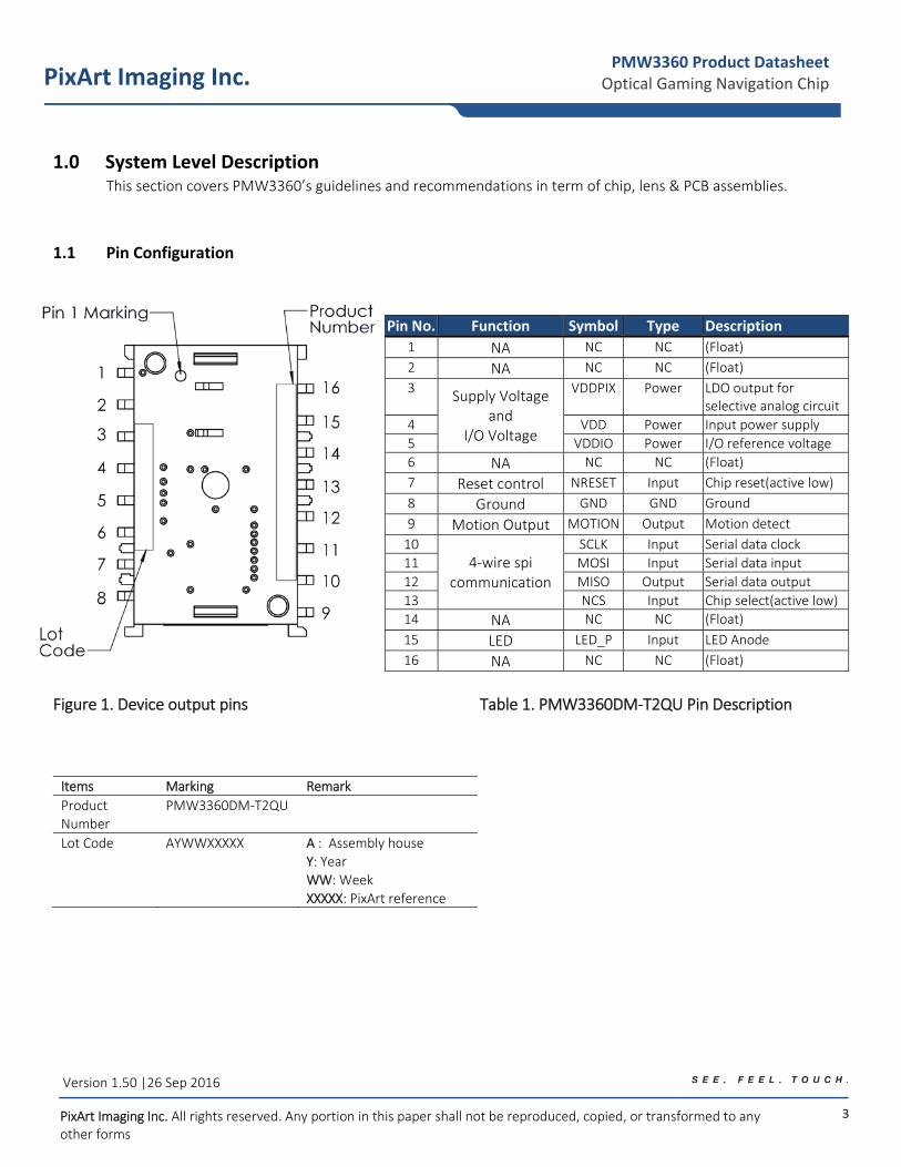
1.0 System Level Description This section covers PMW3360’s guidelines and recommendations in term of chip, lens & PCB assemblies.
1.1 Pin Configuration
Figure 1. Device output pins Table 1. PMW3360DM‐T2QU Pin Description
Items Marking Remark
Product Number
PMW3360DM‐T2QU
Lot Code AYWWXXXXX A : Assembly house
Y: Year WW: Week
XXXXX: PixArt reference
Pin No. Function Symbol Type Description
1 NA NC NC (Float)
2 NA NC NC (Float)
3Supply Voltage
and I/O Voltage
VDDPIX Power LDO output for selective analog circuit
4 VDD Power Input power supply
5 VDDIO Power I/O reference voltage
6 NA NC NC (Float)
7 Reset control NRESET Input Chip reset(active low)
8 Ground GND GND Ground
9 Motion Output MOTION Output Motion detect
10
4‐wire spi communication
SCLK Input Serial data clock
11 MOSI Input Serial data input
12 MISO Output Serial data output
13 NCS Input Chip select(active low)
14 NA NC NC (Float)
15 LED LED_P Input LED Anode
16 NA NC NC (Float)
4
Version 1.50 |26 Sep 2016
PixArt Imaging Inc. All rights reserved. Any portion in this paper shall not be reproduced, copied, or transformed to any other forms
PixArt Imaging Inc. PMW3360 Product Datasheet
Optical Gaming Navigation Chip
1.2 Package Outline Drawing
Figure 2. Package Outline Drawing
CAUTION: It is advised that normal static discharge precautions be taken in handling and assembling of this component to prevent damage and/or degradation which may be induced by ESD.
9.100.358
1.5
2
Pin 1
Pin 1 Indication
16
.20
0.63
8
16X
0.
500.
020
4.110.162
10.100.398
5.050.199
1.
780.
070
0.
890.
035
A
A
Sensor Hole
ProductNumber
LotCode
1
2
3
4
5
6
7
89
10
11
12
13
14
15
16
Pin 1 Marking
10.900.429
At Shoulder 0.
500.
020
0.200.008
10.90 ±0.500.429 ±0.020 At Lead Tip
1.
910.
075
4.
510.
178
1.
710.
067
Z_LF 0.70 ±0.050.028 ±0.002
SECTION A-A
Notes:
1. Dimensions in milimeter[inches]
2. Dimensional tolerance: 0.1mm3. Coplanarity of lead:0.1mm4. Lead pitch tolerance: 0.15mm5. Non-cumulative pitch tolerance: 0.15mm6. Maximum flash:0.2mm7. Angular tolerance: 38. Chamfer (25 x2) on the taper side of the lead9. Brackets () indicate reference dimension10.Document Number:LED_INT_16A_Pkg_007
5
Version 1.50 |26 Sep 2016
PixArt Imaging Inc. All rights reserved. Any portion in this paper shall not be reproduced, copied, or transformed to any other forms
PixArt Imaging Inc. PMW3360 Product Datasheet
Optical Gaming Navigation Chip
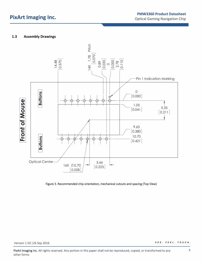
1.3 Assembly Drawings
Figure 3. Recommended chip orientation, mechanical cutouts and spacing (Top View)
16X 0.700.028
0
0.00
0
2.
780.
110
0.
890.
035
14X
1.78
0.07
0 P
itch
14
.48
0.57
0
00.000
1.050.041
9.650.380
10.700.421
5.350.211
5.660.223
Butto
nsBu
ttons
Optical Center
Pin 1 Indication Marking
Fron
t of M
ouse
6
Version 1.50 |26 Sep 2016
PixArt Imaging Inc. All rights reserved. Any portion in this paper shall not be reproduced, copied, or transformed to any other forms
PixArt Imaging Inc. PMW3360 Product Datasheet
Optical Gaming Navigation Chip
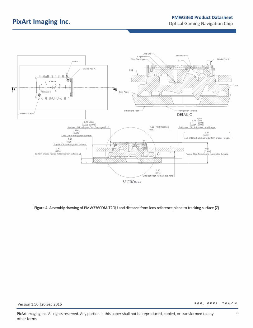
Figure 4. Assembly drawing of PMW3360DM‐T2QU and distance from lens reference plane to tracking surface (Z)
B B
Pin 1
Guide Post A
Guide Post B
1.600.063
PCB Thickness
2.900.114
Gap between PCB & Base Plate
0.70 ±0.050.028 ±0.002
Bottom of LF to Top of Chip Package (Z_LF)
6.71 +-0.080.04
0.264 +-0.0030.002
Bottom of LF to Bottom of Lens Flange
7.410.292
Top of Chip Package to Bottom of Lens Flange
9.810.386
Top of Chip Package to Navigation Surface
2.400.094
Bottom of Lens Flange to Navigation Surface (Z)
7.400.291
Top of PCB to Navigation Surface
8.840.348
Chip Die to Navigation Surface
C
SECTION B-B
PCB
Base Plate
Base Plate Foot Navigation Surface
Lens
LED Hole
Guide Post AChip Hole
Chip Package
Chip Die
LED
DETAIL C
7
Version 1.50 |26 Sep 2016
PixArt Imaging Inc. All rights reserved. Any portion in this paper shall not be reproduced, copied, or transformed to any other forms
PixArt Imaging Inc. PMW3360 Product Datasheet
Optical Gaming Navigation Chip
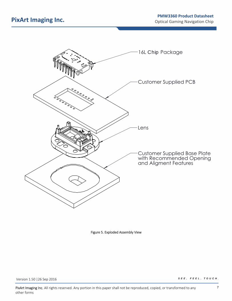
Figure 5. Exploded Assembly View
16L Chip Package
Customer Supplied PCB
Lens
Customer Supplied Base Platewith Recommended Opening and Aligment Features
8
Version 1.50 |26 Sep 2016
PixArt Imaging Inc. All rights reserved. Any portion in this paper shall not be reproduced, copied, or transformed to any other forms
PixArt Imaging Inc. PMW3360 Product Datasheet
Optical Gaming Navigation Chip
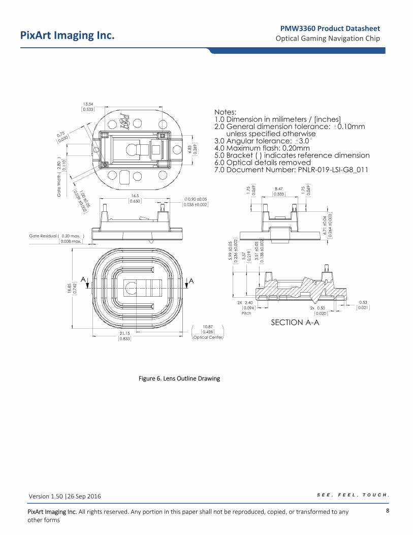
Figure 6. Lens Outline Drawing
18
.85
0.74
2
21.150.833
10.870.428
Optical Center
A A
0.90 ±0.050.035 ±0.002
16.50.650
Gate Residual ( 0.20 max.0.008 max.
) 6.
71 ±
0.04
0.26
4 ±0
.002
8.470.333
1.
750.
069
1.
750.
069
Gat
e W
idth
(2.
800.
110
)
1.00 ±0.05
0.039 ±0.002
0.75
0.030
6.
830.
269
13.540.533
3.
51 ±
0.05
0.13
8 ±0
.002
5.
99 ±
0.05
0.23
6 ±0
.002
5.
570.
219
0.530.021
2x 0.50
0.020
2X 2.400.094
Pitch
SECTION A-A
Notes:1.0 Dimension in milimeters / [inches]2.0 General dimension tolerance: 0.10mm unless specified otherwise3.0 Angular tolerance: 3.04.0 Maximum flash: 0.20mm5.0 Bracket ( ) indicates reference dimension6.0 Optical details removed7.0 Document Number: PNLR-019-LSI-G8_011
9
Version 1.50 |26 Sep 2016
PixArt Imaging Inc. All rights reserved. Any portion in this paper shall not be reproduced, copied, or transformed to any other forms
PixArt Imaging Inc. PMW3360 Product Datasheet
Optical Gaming Navigation Chip
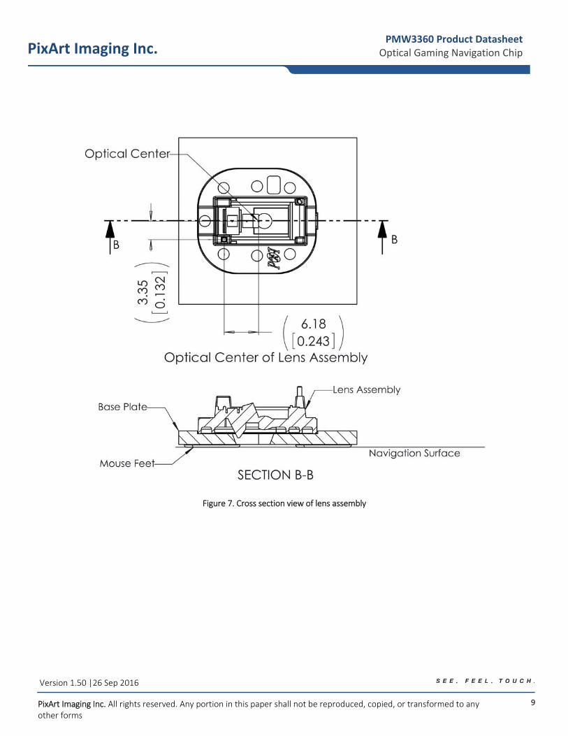
Figure 7. Cross section view of lens assembly
10
Version 1.50 |26 Sep 2016
PixArt Imaging Inc. All rights reserved. Any portion in this paper shall not be reproduced, copied, or transformed to any other forms
PixArt Imaging Inc. PMW3360 Product Datasheet
Optical Gaming Navigation Chip
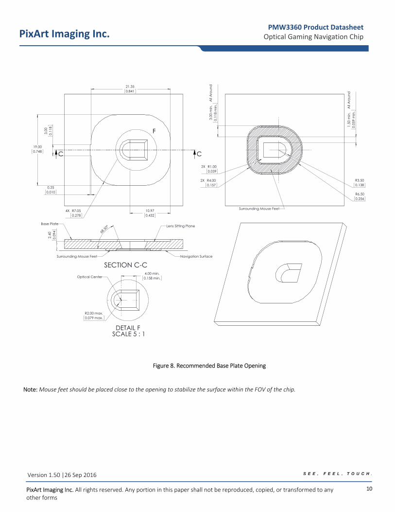
Figure 8. Recommended Base Plate Opening
Note: Mouse feet should be placed close to the opening to stabilize the surface within the FOV of the chip.
21.350.841
19.000.748
10.970.432
3.
000.
118
4X R7.050.278
0.250.010
C C
F
68.50
°
2.
400.
094
Navigation Surface
Base Plate Lens Sitting Plane
SECTION C-CSurrounding Mouse Feet
4.00 min.0.158 min.
R2.00 max.0.079 max.
DETAIL F SCALE 5 : 1
Optical Center
3.00
min
.0.
118
min
. A
ll Aro
und
1.50
min
.0.
059
min
. A
ll Aro
und
2X R1.000.039
2X R4.000.157
R3.500.138
R6.500.256
Surrounding Mouse Feet
11
Version 1.50 |26 Sep 2016
PixArt Imaging Inc. All rights reserved. Any portion in this paper shall not be reproduced, copied, or transformed to any other forms
PixArt Imaging Inc. PMW3360 Product Datasheet
Optical Gaming Navigation Chip
1.4 PCB Assembly Recommendation
1) Insert the integrated chip and all other electrical components into PCB.
2) Wave‐solder the entire assembly in a no‐wash solder process utilizing solder‐fixture. A solder‐fixture is required to
protect the chip from flux spray and wave solder.
3) Avoid getting any solder flux onto the chip body as there is potential for flux to seep into the chip package, the solder
fixture should be designed to expose only the chip leads to flux spray & molten solder while shielding the chip body
and optical apertures. The fixture should also set the chip at the correct position and height on the PCB.
4) Place the lens onto the base plate. Care must be taken to avoid contamination on the optical surfaces.
5) Remove the protective kapton tapes from optical apertures of the chip. Care must be taken to prevent Contaminants
from entering the apertures. Do not place the PCB with the chip facing up during the entire mouse assembly process.
Hold the PCB vertically when removing kapton tape.
6) Insert PCB assembly over the lens onto the base plate aligning post to retain PCB assembly. The chip package will self‐
align to the lens via the guide posts. The optical position reference for the PCB is set by the base plate and lens. Note
that the PCB motion due to button presses must be minimized to maintain optical alignment.
7) Recommendation: The lens can be permanently secured to the chip package by melting the lens’ guide posts over the
chip with heat staking process. Please refer to the application note PMS0122‐LM19‐LSI‐AN for more details.
8) Install mouse top case. There must be a feature in the top case to press down onto the PCB assembly to ensure all
components are stacked or interlocked to the correct vertical height.
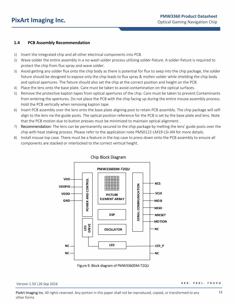
Chip Block Diagram
Figure 9. Block diagram of PMW3360DM‐T2QU
SERIAL CO
MMUNICATION
PICTURE ELEMENT ARRAY
NCS
SCLK
MOTION
MOSI
PMW3360DM‐T2QU
DSP
OSCILLATORLED
DRIVE
POWER
AND CONTROL
VDDO
VDD
GND
MISO
NRESET
VDDPIX
NC
LED_P
NC
LED NC
NC
12
Version 1.50 |26 Sep 2016
PixArt Imaging Inc. All rights reserved. Any portion in this paper shall not be reproduced, copied, or transformed to any other forms
PixArt Imaging Inc. PMW3360 Product Datasheet
Optical Gaming Navigation Chip
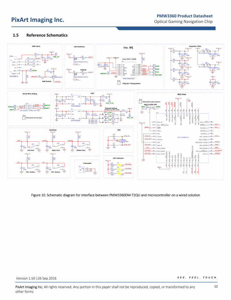
1.5 Reference Schematics
Figure 10. Schematic diagram for interface between PMW3360DM‐T2QU and microcontroller on a wired solution
V+1
DATA-2
DATA+3
ID4
GND5
SHIELD0
CON1
USB_MINIB_5PR10R
1TP3
R3
33RR4
33R
D-
D+
R2
1.5k
USB_SWC110uF
C2100nF
R5
0R
USB_5V
1TP1
1 2
3 4
5 6
J1
PCB_SOCKET_1.27MM_2X3P
SWDIORESETSWCLK
SWO
1TP5
1TP7
1TP6
1TP8
Serial Wire Debug
USB Input
COM3
B2
A1
Q1
Z-Encoder
ZBZA
1
3
2
SW1
Left Click
1
3
2
SW2
Right Click
1
3
2
SW3
Middle Click
C28100nF
C27100nF
R2510k
R2310k
VDD_3.3V VDD_3.3V
LEFT RIGHT MIDDLE
R2710k
VDD_3.3V
C29100nF
1
3
2
SW4
CPI+ Button
CPI+
R2410k
VDD_3.3V
C32100nF
1
3
2
SW5
CPI- Button
CPI-
R2610k
VDD_3.3V
C33100nF
Switches
D1
YLW
R28
470RD2
YLW
R29
470RD3
YLW
R30
470R
VDD_3.3V
CPI_LED1
CPI_LED2
CPI_LED3
CPI Indicator
RESET3
PIO0_14
PIO1_19/DTR/SSEL12
TDI/PIO0_1132
PIO0_22/MISO130
SWCLK/PIO0_10/SCK029
PIO0_9/MOSI028
PIO0_8/MISO027
PIO1_251
XTALOUT7
VDD8
PIO1_21/DCD/MISO126
PIO
1_28/SCLK
24
PIO
0_7/CTS
23
PIO
0_6/USB_CONNECT/SCK0
22
PIO
1_24
21
USB_DP
20
USB_DM
19
PIO1_3125
PIO
1_23/SSEL1
18
PIO
0_21/M
OSI1
17
PIO
0_5/SDA
16
XTALIN6
VSS5
PIO0_209
PIO0_2/SSEL010
PIO1_26/RXD11
PIO1_27/TXD12
PIO
1_20/D
SR/SCK1
13
PIO
0_3/USB_VBUS
14
PIO
0_4/SCL
15
PIO
0_16/W
AKEUP
40
SWDIO
/PIO
0_15
39
PIO
1_22/RI/MOSI1
38
PIO
1_14/D
SR/RXD
37
PIO1_13/DTR36
TRST/PIO0_1435
TMS/PIO0_1233
PIO1_29/SCK031
TDO/PIO0_1334
VSS
41
PIO
0_23
42
PIO
1_15/D
CD/SCK1
43
VDD
44
PIO
0_17/RTS/SCLK
45
PIO
0_18/RXD
46
PIO
0_19/TXD
47
PIO
1_16/RI
48
U3
LPC11U34FBD48/311
C31
18pF
VDD1_3.3V
CP
I+
CP
I-
MISO
MOSI
SCLK
NCS
LE
FT
RIG
HT
MID
DL
E
ZA
ZB
D-
D+
C30
18pF
MOTION
MCU Part
13
24
X112MHz
CPI_LED1
CPI_LED2
CPI_LED3
SWCLK
SW
DIO
US
B_
CO
N
USB_5V
RESET
SN_NRESET
SW_1
SW_2
VDD2_3.3V
XTAL_OUT
XTAL_IN
XTAL_OUT
XTAL_IN
OSC
USB Switch
c3
b1
e2
Q2MMBT3906LT1
VDD_3.3V
R7
10k
R6
2.2k
USB_CON
USB_SW
R11
0RC510uF
C8100nF
VDD1_3.3V
R12
0RC610uF
C9100nF
VDD2_3.3V
R13
0RC710uF
C10100nF
VDD3_3.3V
R22
0RC2310uF
C24100nF
VDD4_3.3V
VDD_3.3V
C1110uF
C13100nF
VDD5_SS
C1210uF
C14100nF
VDD6_SS
VDD_SS
21 J2
PH_2.54MM_1X2P
21J3
PH_2.54MM_1X2P
JP2
JP3
C2510uF
C26100nF
USB_5V
Capacitor Filter
d3
s2
g1
Q3
BSS223PWH6327XTSA1
SW_1
R8
20R
VDD5_SS
LED1_P
d3
s2
g1
Q4
BSS223PWH6327XTSA1
SW_2
R9
39R
VDD5_SS
LED1_P
LED Switches
1
NC2
VDDPIX3
6
VDD4
VDDIO5
LED_P15
NC14
NCS13
MISO12
MOSI11
SCLK10
MOTION9
NRESET7
NC16
GND8
U6
PWM3360DM-T2QU
R1010k
MISOMOSI
VDD6_SS
SCLK
NCS
MOTION
VDD_3.3V
LED_P
NRESET1TP9
1TP17
1TP16
1TP15
1TP12
Insert RCPT 1.02MM
PCB1
1 Placement at Top Layer
IN1
EN3
FB4
GND2
OUT5
U1
TPS73601DBVR
C171uF
C15100nF
USB_5V
C2110uF
C19100nF
R1452.3k
R16
30.1k
R17
0R
1
TP2
VDD_3.3V
IN1
EN3
FB4
GND2
OUT5
U2
TPS73601DBVR
C181uF
C16100nF
USB_5V
C2210uF
C20100nF
R18
56k
R21
0R
1
TP2
VDD_SS
R1537.4k
2.0V
1.9V
1.8V
LDO
1
2
3
SW6SLIDE SW SPDTGND OPEN
R19
63.4kR20
75k
21J4
PH_2MM_1X2P
21 J5
PH_2MM_1X2P 21J6
PH_2MM_1X2P
JP4
JP5
JP6
AGND
USB_5V
NRESET
MISO
MOSI
SCLK
MOTION
SWCLK
SWO
SWDIO
RESET
VCC_3.3V
VCC_SS
PCB2
2
Slide Switch place bottom.
PCB3
3
Default
MCU FLASH OPT1
Default SettingJ5 Short by JP5 (1.9V)
NC
NCC34.7uF/10V
C4100nF
VDD6_SSVDD4_3.3V
Chip pin 1 facing down
Chip .ƭƻŎƪ
13
Version 1.50 |26 Sep 2016
PixArt Imaging Inc. All rights reserved. Any portion in this paper shall not be reproduced, copied, or transformed to any other forms
PixArt Imaging Inc. PMW3360 Product Datasheet
Optical Gaming Navigation Chip
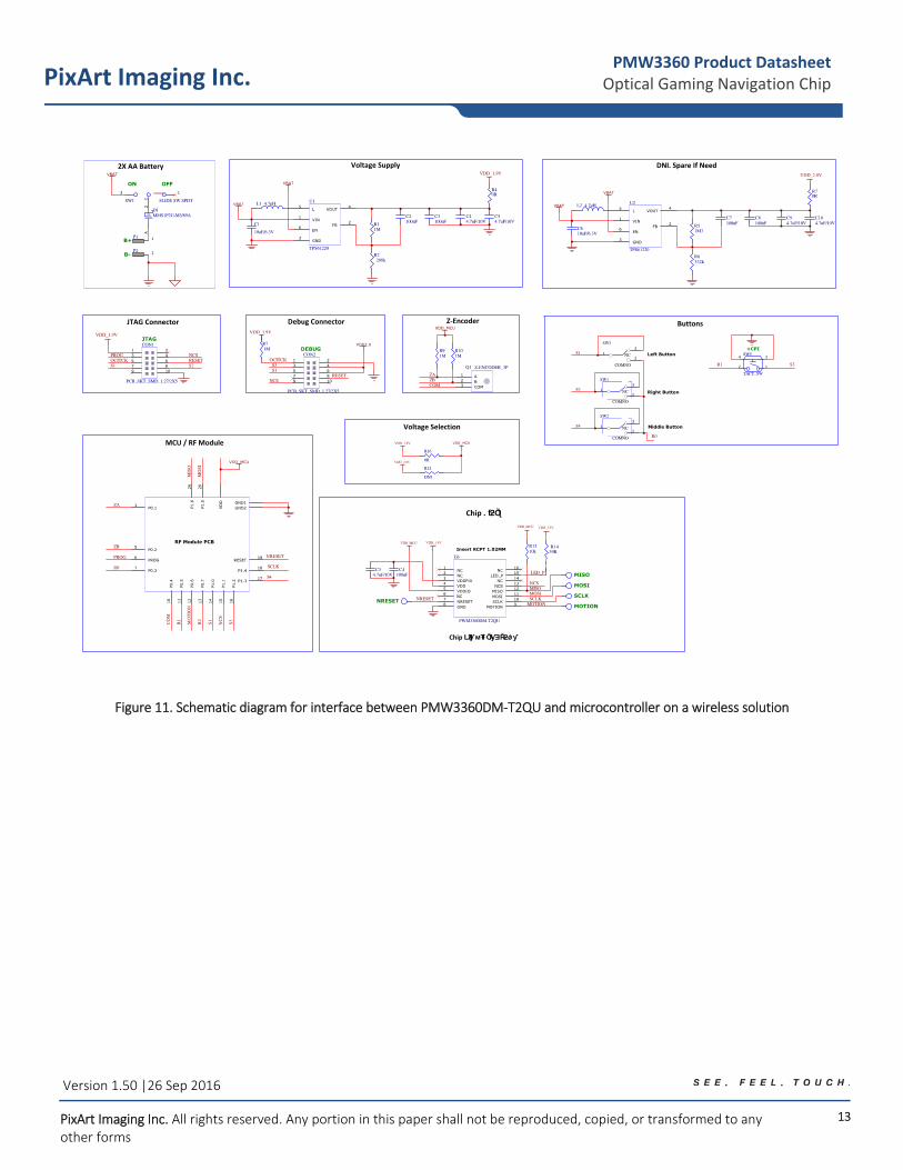
Figure 11. Schematic diagram for interface between PMW3360DM‐T2QU and microcontroller on a wireless solution
Chip LJƛƴ м ŦŀŎƛƴƎ Řƻǿƴ
Chip .ƭƻŎƪ
14
Version 1.50 |26 Sep 2016
PixArt Imaging Inc. All rights reserved. Any portion in this paper shall not be reproduced, copied, or transformed to any other forms
PixArt Imaging Inc. PMW3360 Product Datasheet
Optical Gaming Navigation Chip
2.0 Electrical Specifications
Regulatory Requirements
• Passes FCC “Part15, Subpart B, Class B”, “CISPR 22 1997 Class B” and worldwide analogous emission limits when assembled into a mouse with shielded cable and following PixArt Imaging’s recommendations.
• Passes IEC 62471: 2006 Photo biological safety of lamps and lamp systems
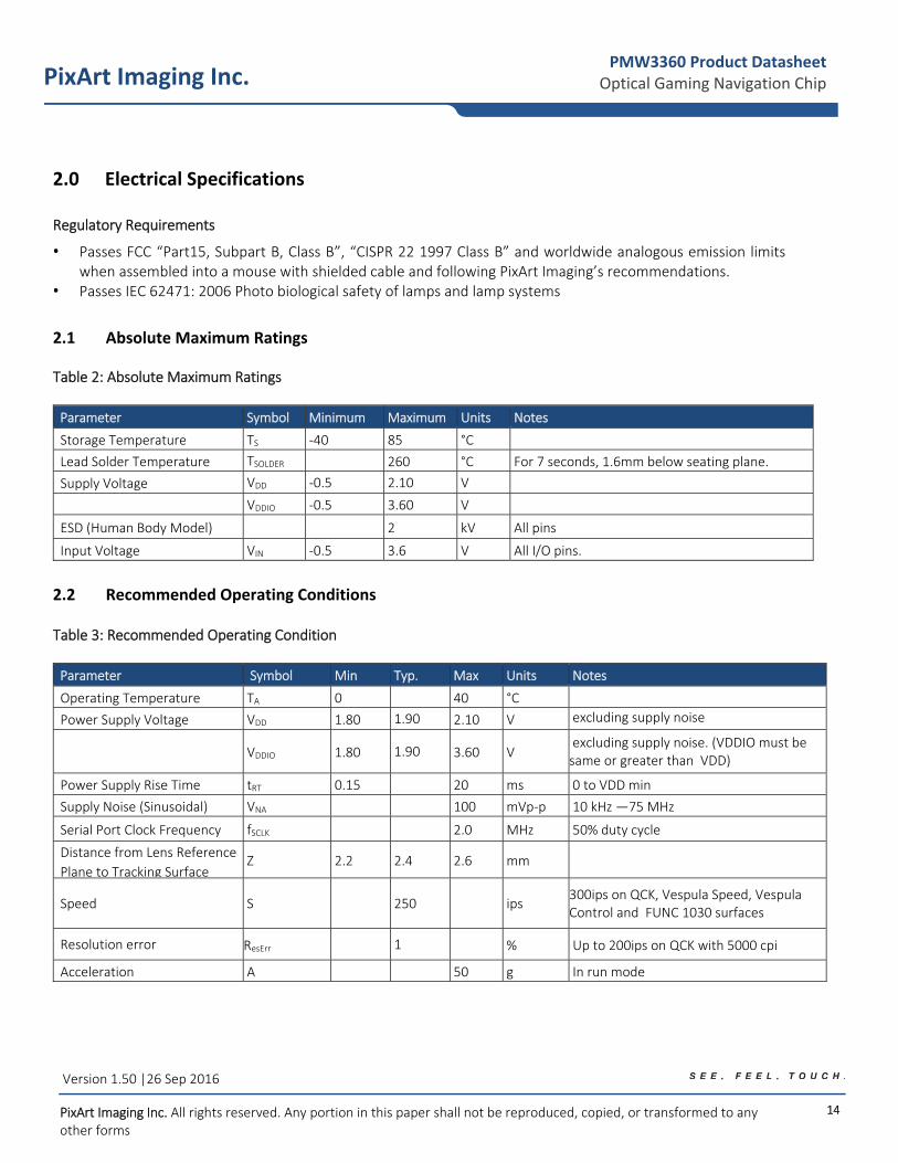
2.1 Absolute Maximum Ratings Table 2: Absolute Maximum Ratings
Parameter Symbol Minimum Maximum Units Notes
Storage Temperature TS ‐40 85 °C
Lead Solder Temperature TSOLDER 260 °C For 7 seconds, 1.6mm below seating plane.
Supply Voltage VDD ‐0.5 2.10 V
VDDIO ‐0.5 3.60 V
ESD (Human Body Model) 2 kV All pins
Input Voltage VIN ‐0.5 3.6 V All I/O pins.
2.2 Recommended Operating Conditions Table 3: Recommended Operating Condition
Parameter Symbol Min Typ. Max Units Notes
Operating Temperature TA 0 40 °C
Power Supply Voltage VDD 1.80 1.90 2.10 V excluding supply noise
VDDIO 1.80 1.90 3.60 V excluding supply noise. (VDDIO must be same or greater than VDD)
Power Supply Rise Time tRT 0.15 20 ms 0 to VDD min
Supply Noise (Sinusoidal) VNA 100 mVp‐p 10 kHz —75 MHz
Serial Port Clock Frequency fSCLK 2.0 MHz 50% duty cycle
Distance from Lens Reference
Plane to Tracking Surface Z 2.2 2.4 2.6 mm
Speed S 250 ips 300ips on QCK, Vespula Speed, Vespula Control and FUNC 1030 surfaces
Resolution error ResErr 1 % Up to 200ips on QCK with 5000 cpi
Acceleration A 50 g In run mode
15
Version 1.50 |26 Sep 2016
PixArt Imaging Inc. All rights reserved. Any portion in this paper shall not be reproduced, copied, or transformed to any other forms
PixArt Imaging Inc. PMW3360 Product Datasheet
Optical Gaming Navigation Chip
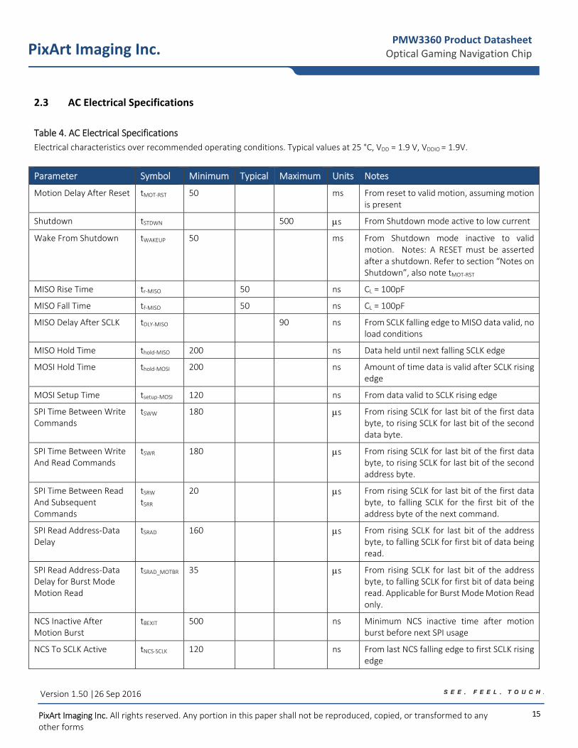
2.3 AC Electrical Specifications
Table 4. AC Electrical Specifications
Electrical characteristics over recommended operating conditions. Typical values at 25 °C, VDD = 1.9 V, VDDIO = 1.9V.
Parameter Symbol Minimum Typical Maximum Units Notes
Motion Delay After Reset tMOT‐RST 50 ms From reset to valid motion, assuming motion is present
Shutdown tSTDWN 500 s From Shutdown mode active to low current
Wake From Shutdown tWAKEUP 50 ms From Shutdown mode inactive to valid motion. Notes: A RESET must be asserted after a shutdown. Refer to section “Notes on Shutdown”, also note tMOT‐RST
MISO Rise Time tr‐MISO 50 ns CL = 100pF
MISO Fall Time tf‐MISO 50 ns CL = 100pF
MISO Delay After SCLK tDLY‐MISO 90 ns From SCLK falling edge to MISO data valid, no load conditions
MISO Hold Time thold‐MISO 200 ns Data held until next falling SCLK edge
MOSI Hold Time thold‐MOSI 200 ns Amount of time data is valid after SCLK rising edge
MOSI Setup Time tsetup‐MOSI 120 ns From data valid to SCLK rising edge
SPI Time Between Write Commands
tSWW 180 s From rising SCLK for last bit of the first data byte, to rising SCLK for last bit of the second data byte.
SPI Time Between Write And Read Commands
tSWR 180 s From rising SCLK for last bit of the first data byte, to rising SCLK for last bit of the second address byte.
SPI Time Between Read And Subsequent Commands
tSRW
tSRR 20 s From rising SCLK for last bit of the first data
byte, to falling SCLK for the first bit of the address byte of the next command.
SPI Read Address‐Data Delay
tSRAD 160 s From rising SCLK for last bit of the address byte, to falling SCLK for first bit of data being read.
SPI Read Address‐Data Delay for Burst Mode Motion Read
tSRAD_MOTBR 35 s From rising SCLK for last bit of the address byte, to falling SCLK for first bit of data being read. Applicable for Burst Mode Motion Read only.
NCS Inactive After Motion Burst
tBEXIT 500 ns Minimum NCS inactive time after motion burst before next SPI usage
NCS To SCLK Active tNCS‐SCLK 120 ns From last NCS falling edge to first SCLK rising edge
16
Version 1.50 |26 Sep 2016
PixArt Imaging Inc. All rights reserved. Any portion in this paper shall not be reproduced, copied, or transformed to any other forms
PixArt Imaging Inc. PMW3360 Product Datasheet
Optical Gaming Navigation Chip
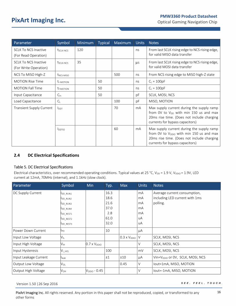
Parameter Symbol Minimum Typical Maximum Units Notes
SCLK To NCS Inactive
(For Read Operation)
tSCLK‐NCS 120 ns From last SCLK rising edge to NCS rising edge, for valid MISO data transfer
SCLK To NCS Inactive
(For Write Operation)
tSCLK‐NCS 35 s From last SCLK rising edge to NCS rising edge, for valid MOSI data transfer
NCS To MISO High‐Z tNCS‐MISO 500 ns From NCS rising edge to MISO high‐Z state
MOTION Rise Time tr‐MOTION 50 ns CL = 100pF
MOTION Fall Time tf‐MOTION 50 ns CL = 100pF
Input Capacitance Cin 50 pF SCLK, MOSI, NCS
Load Capacitance CL 100 pF MISO, MOTION
Transient Supply Current IDDT 70 mA Max supply current during the supply ramp from 0V to VDD with min 150 us and max 20ms rise time. (Does not include charging currents for bypass capacitors)
IDDTIO 60 mA Max supply current during the supply ramp from 0V to VDDIO with min 150 us and max 20ms rise time. (Does not include charging currents for bypass capacitors)
2.4 DC Electrical Specifications
Table 5. DC Electrical Specifications
Electrical characteristics, over recommended operating conditions. Typical values at 25 °C, VDD = 1.9 V, VDDIO = 1.9V, LED current at 12mA, 70MHz (internal), and 1.1kHz (slow clock).
Parameter Symbol Min Typ. Max Units Notes
DC Supply Current IDD_RUN1 IDD_RUN2 IDD_RUN3 IDD_RUN4 IDD_REST1 IDD_REST2 IDD_REST3
16.3
18.6
21.6
37.0
2.8
61.0
32.0
mA
mA
mA
mA
mA
uA
uA
Average current consumption,
including LED current with 1ms
polling.
Power Down Current IPD 10 µA
Input Low Voltage VIL 0.3 x VDDIO V SCLK, MOSI, NCS
Input High Voltage VIH 0.7 x VDDIO V SCLK, MOSI, NCS
Input Hysteresis VI_HYS 100 mV SCLK, MOSI, NCS
Input Leakage Current Ileak ±1 ±10 µA Vin=VDDIO or 0V, SCLK, MOSI, NCS
Output Low Voltage VOL 0.45 V Iout=1mA, MISO, MOTION
Output High Voltage VOH VDDIO ‐ 0.45 V Iout=‐1mA, MISO, MOTION
17
Version 1.50 |26 Sep 2016
PixArt Imaging Inc. All rights reserved. Any portion in this paper shall not be reproduced, copied, or transformed to any other forms
PixArt Imaging Inc. PMW3360 Product Datasheet
Optical Gaming Navigation Chip
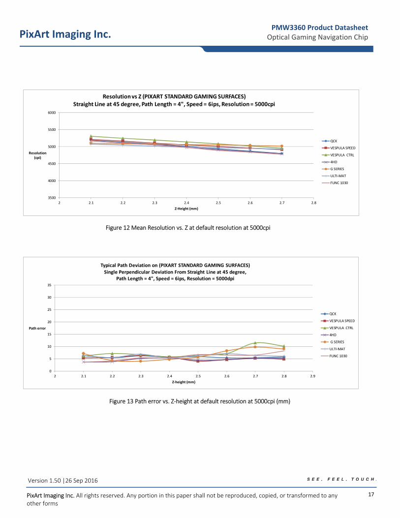
Figure 12 Mean Resolution vs. Z at default resolution at 5000cpi
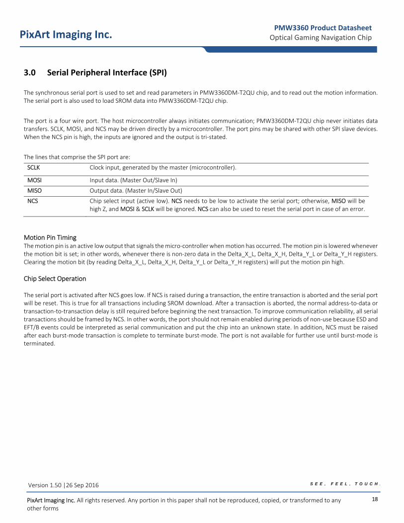
Figure 13 Path error vs. Z‐height at default resolution at 5000cpi (mm)
3500
4000
4500
5000
5500
6000
2 2.1 2.2 2.3 2.4 2.5 2.6 2.7 2.8
Resolution (cpi)
Z‐Height (mm)
Resolution vs Z (PIXART STANDARD GAMING SURFACES)Straight Line at 45 degree, Path Length = 4", Speed = 6ips, Resolution = 5000cpi
QCK
VESPULA SPEED
VESPULA CTRL
4HD
G SERIES
ULTI‐MAT
FUNC 1030
0
5
10
15
20
25
30
35
2 2.1 2.2 2.3 2.4 2.5 2.6 2.7 2.8 2.9
Path error
Z‐height (mm)
Typical Path Deviation on (PIXART STANDARD GAMING SURFACES)
Single Perpendicular Deviation From Straight Line at 45 degree, Path Length = 4", Speed = 6ips, Resolution = 5000dpi
QCK
VESPULA SPEED
VESPULA CTRL
4HD
G SERIES
ULTI‐MAT
FUNC 1030
18
Version 1.50 |26 Sep 2016
PixArt Imaging Inc. All rights reserved. Any portion in this paper shall not be reproduced, copied, or transformed to any other forms
PixArt Imaging Inc. PMW3360 Product Datasheet
Optical Gaming Navigation Chip
3.0 Serial Peripheral Interface (SPI) The synchronous serial port is used to set and read parameters in PMW3360DM‐T2QU chip, and to read out the motion information. The serial port is also used to load SROM data into PMW3360DM‐T2QU chip.
The port is a four wire port. The host microcontroller always initiates communication; PMW3360DM‐T2QU chip never initiates data transfers. SCLK, MOSI, and NCS may be driven directly by a microcontroller. The port pins may be shared with other SPI slave devices. When the NCS pin is high, the inputs are ignored and the output is tri‐stated.
The lines that comprise the SPI port are:
Motion Pin Timing The motion pin is an active low output that signals the micro‐controller when motion has occurred. The motion pin is lowered whenever the motion bit is set; in other words, whenever there is non‐zero data in the Delta_X_L, Delta_X_H, Delta_Y_L or Delta_Y_H registers. Clearing the motion bit (by reading Delta_X_L, Delta_X_H, Delta_Y_L or Delta_Y_H registers) will put the motion pin high.
Chip Select Operation The serial port is activated after NCS goes low. If NCS is raised during a transaction, the entire transaction is aborted and the serial port will be reset. This is true for all transactions including SROM download. After a transaction is aborted, the normal address‐to‐data or transaction‐to‐transaction delay is still required before beginning the next transaction. To improve communication reliability, all serial transactions should be framed by NCS. In other words, the port should not remain enabled during periods of non‐use because ESD and EFT/B events could be interpreted as serial communication and put the chip into an unknown state. In addition, NCS must be raised after each burst‐mode transaction is complete to terminate burst‐mode. The port is not available for further use until burst‐mode is terminated.
SCLK Clock input, generated by the master (microcontroller).
MOSI Input data. (Master Out/Slave In)
MISO Output data. (Master In/Slave Out)
NCS Chip select input (active low). NCS needs to be low to activate the serial port; otherwise, MISO will be high Z, and MOSI & SCLK will be ignored. NCS can also be used to reset the serial port in case of an error.
19
Version 1.50 |26 Sep 2016
PixArt Imaging Inc. All rights reserved. Any portion in this paper shall not be reproduced, copied, or transformed to any other forms
PixArt Imaging Inc. PMW3360 Product Datasheet
Optical Gaming Navigation Chip
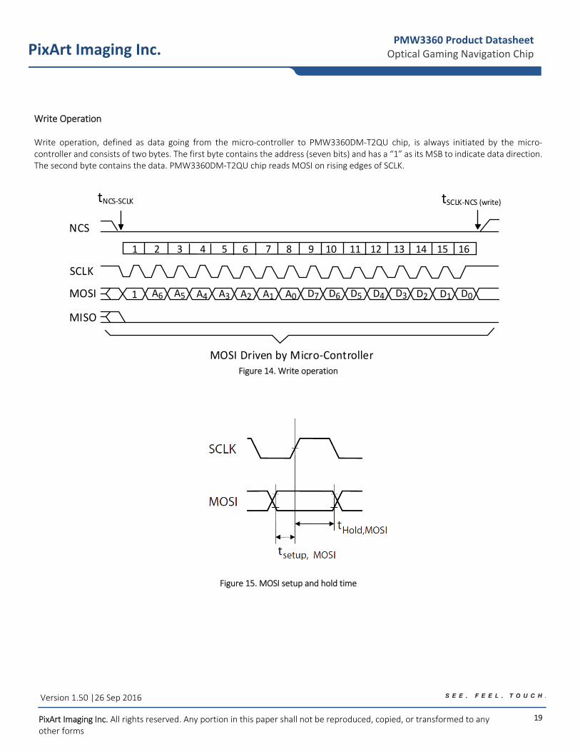
Write Operation Write operation, defined as data going from the micro‐controller to PMW3360DM‐T2QU chip, is always initiated by the micro‐controller and consists of two bytes. The first byte contains the address (seven bits) and has a “1” as its MSB to indicate data direction. The second byte contains the data. PMW3360DM‐T2QU chip reads MOSI on rising edges of SCLK.
MOSI Driven by Micro‐Controller
1 2 3 4 5 6 7 8 9 10 11 12 13 14 15 16
A6 A5 A4 D7 D5 D4 D3 D2 D1 D0D6
NCS
SCLK
MOSI
MISO
1 A3 A2 A1 A0
tSCLK‐NCS (write)tNCS‐SCLK
Figure 14. Write operation
Figure 15. MOSI setup and hold time
20
PixArt Imaging Inc. PMW3360 Product Datasheet
Optical Gaming Navigation Chip
Version 1.50 |26 Sep 2016
PixArt Imaging Inc. All rights reserved. Any portion in this paper shall not be reproduced, copied, or transformed to any other forms
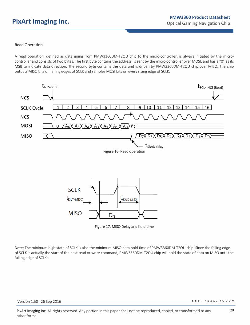
Read Operation
A read operation, defined as data going from PMW3360DM‐T2QU chip to the micro‐controller, is always initiated by the micro‐controller and consists of two bytes. The first byte contains the address, is sent by the micro‐controller over MOSI, and has a “0” as its MSB to indicate data direction. The second byte contains the data and is driven by PMW3360DM‐T2QU chip over MISO. The chip outputs MISO bits on falling edges of SCLK and samples MOSI bits on every rising edge of SCLK.
SCLK Cycle 1 2 3 4 5 6 7 8 9 10 11 12 13 14 15 16
NCS
tSCLK‐NCS (Read)tNCS‐SCLK
NCS
A6 A5 A40 A3 A2 A1 A0MOSI
D5 D4 D3 D2 D1 D0D6D7MISO
tSRAD delay Figure 16. Read operation
Figure 17. MISO Delay and hold time
Note: The minimum high state of SCLK is also the minimum MISO data hold time of PMW3360DM‐T2QU chip. Since the falling edge of SCLK is actually the start of the next read or write command, PMW3360DM‐T2QU chip will hold the state of data on MISO until the falling edge of SCLK.
21
PixArt Imaging Inc. PMW3360 Product Datasheet
Optical Gaming Navigation Chip
Version 1.50 |26 Sep 2016
PixArt Imaging Inc. All rights reserved. Any portion in this paper shall not be reproduced, copied, or transformed to any other forms
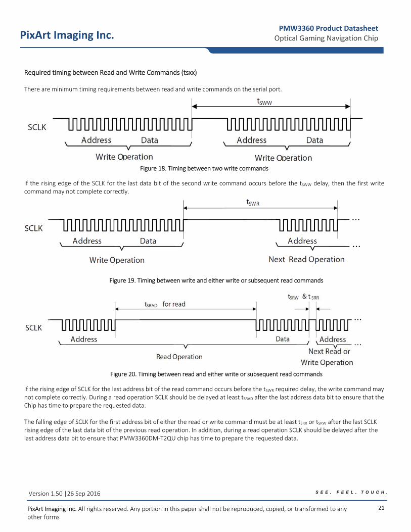
Required timing between Read and Write Commands (tsxx) There are minimum timing requirements between read and write commands on the serial port.
Figure 18. Timing between two write commands
If the rising edge of the SCLK for the last data bit of the second write command occurs before the tSWW delay, then the first write command may not complete correctly.
Figure 19. Timing between write and either write or subsequent read commands
Figure 20. Timing between read and either write or subsequent read commands
If the rising edge of SCLK for the last address bit of the read command occurs before the tSWR required delay, the write command may not complete correctly. During a read operation SCLK should be delayed at least tSRAD after the last address data bit to ensure that the Chip has time to prepare the requested data. The falling edge of SCLK for the first address bit of either the read or write command must be at least tSRR or tSRW after the last SCLK rising edge of the last data bit of the previous read operation. In addition, during a read operation SCLK should be delayed after the last address data bit to ensure that PMW3360DM‐T2QU chip has time to prepare the requested data.
22
PixArt Imaging Inc. PMW3360 Product Datasheet
Optical Gaming Navigation Chip
Version 1.50 |26 Sep 2016
PixArt Imaging Inc. All rights reserved. Any portion in this paper shall not be reproduced, copied, or transformed to any other forms
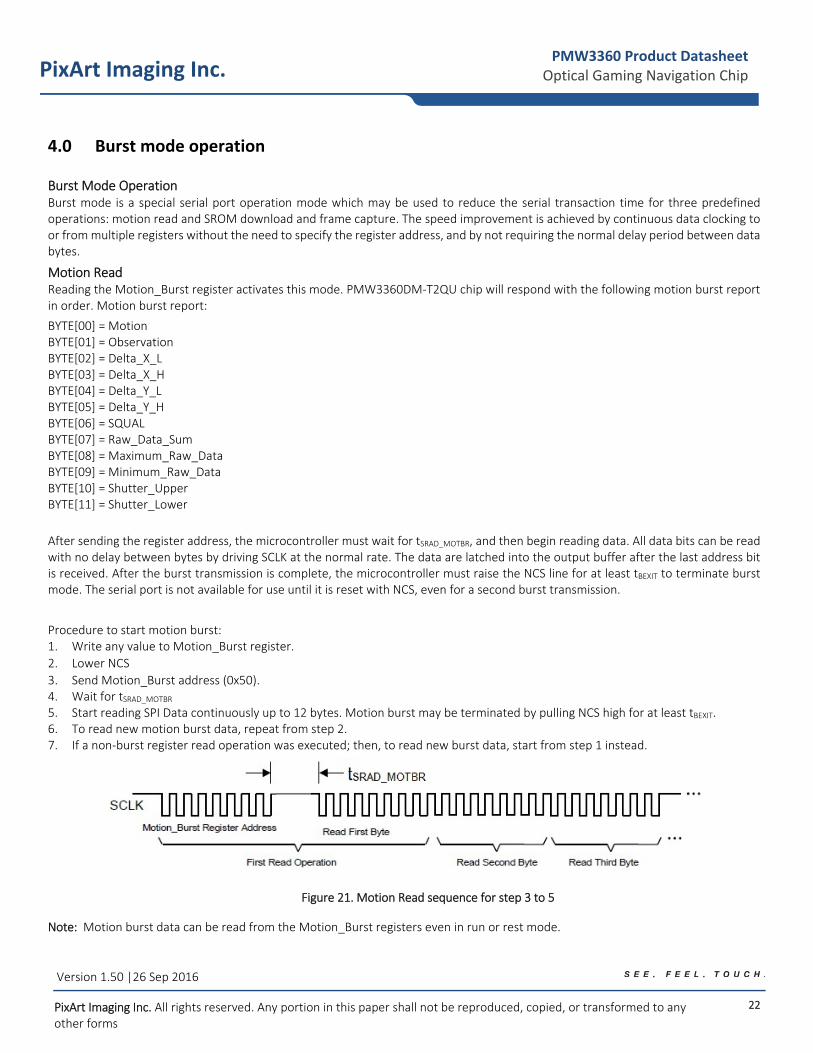
4.0 Burst mode operation Burst Mode Operation Burst mode is a special serial port operation mode which may be used to reduce the serial transaction time for three predefined operations: motion read and SROM download and frame capture. The speed improvement is achieved by continuous data clocking to or from multiple registers without the need to specify the register address, and by not requiring the normal delay period between data bytes.
Motion Read Reading the Motion_Burst register activates this mode. PMW3360DM‐T2QU chip will respond with the following motion burst report in order. Motion burst report:
BYTE[00] = Motion BYTE[01] = Observation BYTE[02] = Delta_X_L BYTE[03] = Delta_X_H BYTE[04] = Delta_Y_L BYTE[05] = Delta_Y_H BYTE[06] = SQUAL BYTE[07] = Raw_Data_Sum BYTE[08] = Maximum_Raw_Data BYTE[09] = Minimum_Raw_Data BYTE[10] = Shutter_Upper BYTE[11] = Shutter_Lower
After sending the register address, the microcontroller must wait for tSRAD_MOTBR, and then begin reading data. All data bits can be read with no delay between bytes by driving SCLK at the normal rate. The data are latched into the output buffer after the last address bit is received. After the burst transmission is complete, the microcontroller must raise the NCS line for at least tBEXIT to terminate burst mode. The serial port is not available for use until it is reset with NCS, even for a second burst transmission.
Procedure to start motion burst: 1. Write any value to Motion_Burst register.
2. Lower NCS
3. Send Motion_Burst address (0x50). 4. Wait for tSRAD_MOTBR 5. Start reading SPI Data continuously up to 12 bytes. Motion burst may be terminated by pulling NCS high for at least tBEXIT. 6. To read new motion burst data, repeat from step 2. 7. If a non‐burst register read operation was executed; then, to read new burst data, start from step 1 instead.
Figure 21. Motion Read sequence for step 3 to 5
Note: Motion burst data can be read from the Motion_Burst registers even in run or rest mode.
23
PixArt Imaging Inc. PMW3360 Product Datasheet
Optical Gaming Navigation Chip
Version 1.50 |26 Sep 2016
PixArt Imaging Inc. All rights reserved. Any portion in this paper shall not be reproduced, copied, or transformed to any other forms
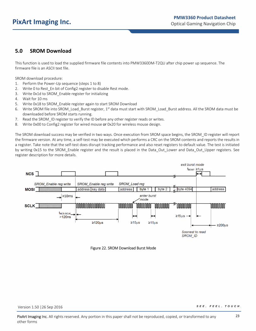
5.0 SROM Download This function is used to load the supplied firmware file contents into PMW3360DM‐T2QU after chip power up sequence. The firmware file is an ASCII text file. SROM download procedure: 1. Perform the Power‐Up sequence (steps 1 to 8) 2. Write 0 to Rest_En bit of Config2 register to disable Rest mode. 3. Write 0x1d to SROM_Enable register for initializing 4. Wait for 10 ms 5. Write 0x18 to SROM_Enable register again to start SROM Download 6. Write SROM file into SROM_Load_Burst register, 1st data must start with SROM_Load_Burst address. All the SROM data must be
downloaded before SROM starts running. 7. Read the SROM_ID register to verify the ID before any other register reads or writes. 8. Write 0x00 to Config2 register for wired mouse or 0x20 for wireless mouse design. The SROM download success may be verified in two ways. Once execution from SROM space begins, the SROM_ID register will report the firmware version. At any time, a self‐test may be executed which performs a CRC on the SROM contents and reports the results in a register. Take note that the self‐test does disrupt tracking performance and also reset registers to default value. The test is initiated by writing 0x15 to the SROM_Enable register and the result is placed in the Data_Out_Lower and Data_Out_Upper registers. See register description for more details.
Figure 22. SROM Download Burst Mode
24
PixArt Imaging Inc. PMW3360 Product Datasheet
Optical Gaming Navigation Chip
Version 1.50 |26 Sep 2016
PixArt Imaging Inc. All rights reserved. Any portion in this paper shall not be reproduced, copied, or transformed to any other forms
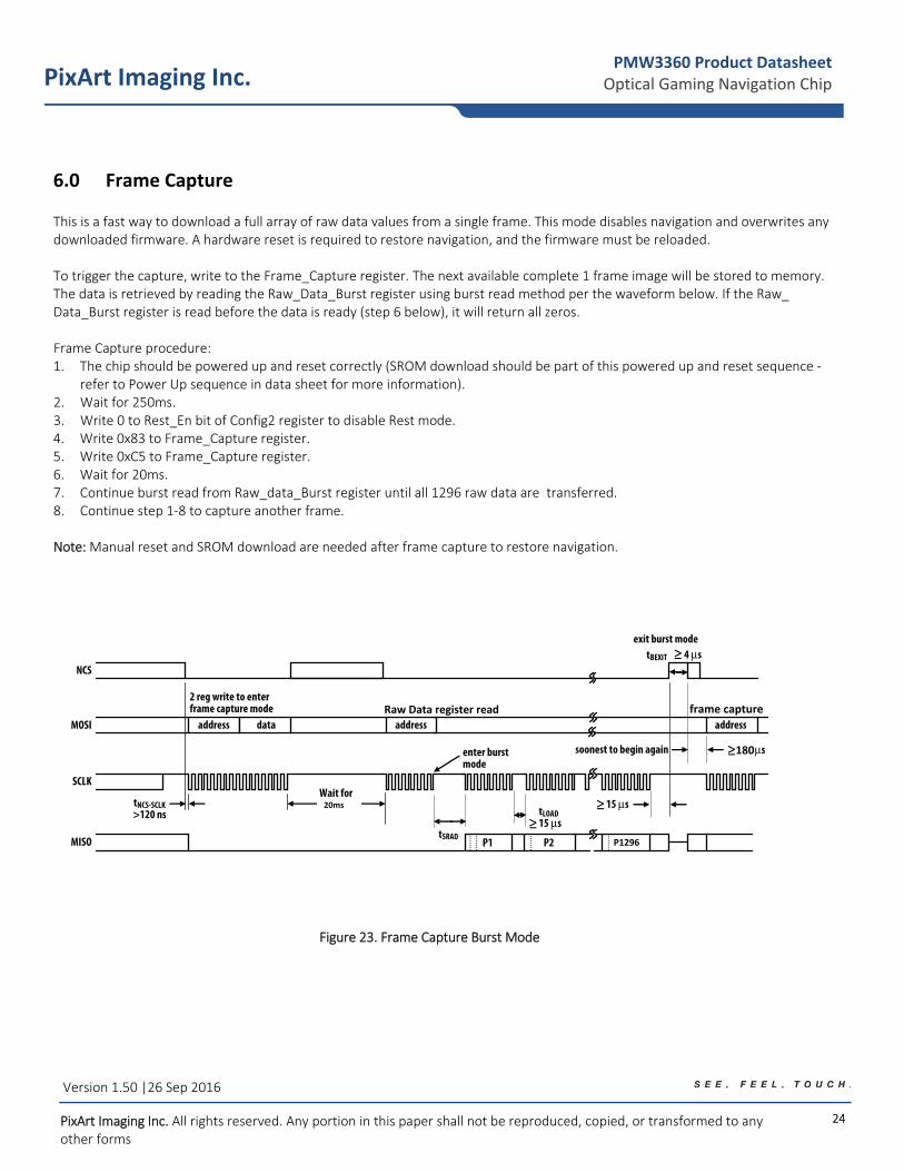
6.0 Frame Capture This is a fast way to download a full array of raw data values from a single frame. This mode disables navigation and overwrites any downloaded firmware. A hardware reset is required to restore navigation, and the firmware must be reloaded. To trigger the capture, write to the Frame_Capture register. The next available complete 1 frame image will be stored to memory. The data is retrieved by reading the Raw_Data_Burst register using burst read method per the waveform below. If the Raw_ Data_Burst register is read before the data is ready (step 6 below), it will return all zeros. Frame Capture procedure: 1. The chip should be powered up and reset correctly (SROM download should be part of this powered up and reset sequence ‐
refer to Power Up sequence in data sheet for more information). 2. Wait for 250ms. 3. Write 0 to Rest_En bit of Config2 register to disable Rest mode. 4. Write 0x83 to Frame_Capture register. 5. Write 0xC5 to Frame_Capture register. 6. Wait for 20ms. 7. Continue burst read from Raw_data_Burst register until all 1296 raw data are transferred. 8. Continue step 1‐8 to capture another frame. Note: Manual reset and SROM download are needed after frame capture to restore navigation.
Figure 23. Frame Capture Burst Mode
tNCS-SCLK>120 ns
exit burst mode4 µstBEXIT
µs
address data address address
P1 P2
SCLK
MOSI
MISO
NCS
2 reg write to enterframe capture mode
enter burstmode
Wait for
tLOAD15 µs
soonest to begin again
tSRAD
Raw Data register read
180
P1296
15 µs
≥
≥
≥
≥
frame capture
20ms
25
PixArt Imaging Inc. PMW3360 Product Datasheet
Optical Gaming Navigation Chip
Version 1.50 |26 Sep 2016
PixArt Imaging Inc. All rights reserved. Any portion in this paper shall not be reproduced, copied, or transformed to any other forms
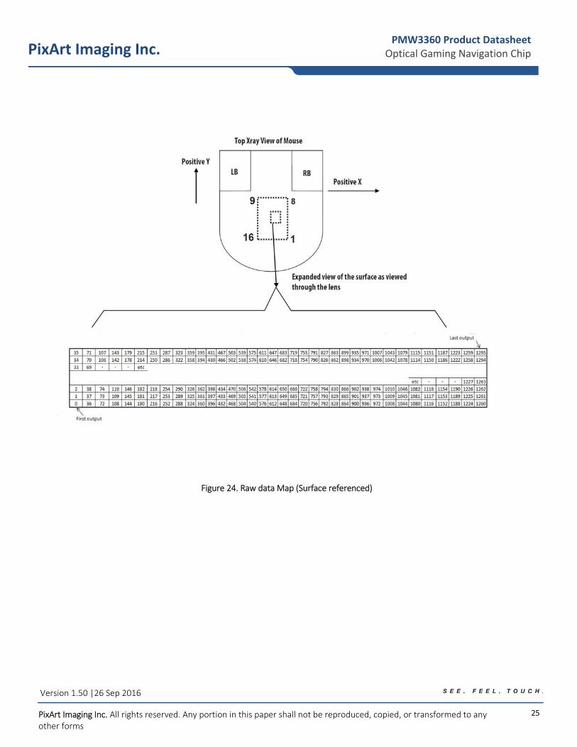
Figure 24. Raw data Map (Surface referenced)

26
PixArt Imaging Inc. PMW3360 Product Datasheet
Optical Gaming Navigation Chip
Version 1.50 |26 Sep 2016
PixArt Imaging Inc. All rights reserved. Any portion in this paper shall not be reproduced, copied, or transformed to any other forms
7.0 Power Up Although the chip performs an internal power up self reset, it is still recommend that the Power_Up_Reset register is written every time power is applied. The appropriate sequence is as follows: 1. Apply power to VDD and VDDIO in any order, with a delay of no more than 100ms in between each supply. Ensure all supplies
are stable.
2. Drive NCS high, and then low to reset the SPI port.
3. Write 0x5A to Power_Up_Reset register (or, alternatively toggle the NRESET pin).
4. Wait for at least 50ms.
5. Read from registers 0x02, 0x03, 0x04, 0x05 and 0x06 one time regardless of the motion pin state.
6. Perform SROM download. 7. Load configuration for other registers. During power‐up there will be a period of time after the power supply is high but before normal operation. The table below shows the state of the various pins during power‐up and reset.
State of Signal Pins After VDD is Valid
Pin During Reset After Reset
NRESET Functional Functional
NCS Ignored Functional
MISO Undefined Depends on NCS
SCLK Ignored Depends on NCS
MOSI Ignored Depends on NCS
MOTION Undefined Functional
NRESET The NRESET pin can be used to perform a full chip reset. When asserted, it performs the same reset function as the Power_Up_Reset_Register. The NRESET pin needs to be asserted (held to logic 0) for at least 100 ns. Note:‐ NRESET pin has a built in weak pull up circuit. During active low reset phase, it can draw a static current of up to 600uA.
27
PixArt Imaging Inc. PMW3360 Product Datasheet
Optical Gaming Navigation Chip
Version 1.50 |26 Sep 2016
PixArt Imaging Inc. All rights reserved. Any portion in this paper shall not be reproduced, copied, or transformed to any other forms
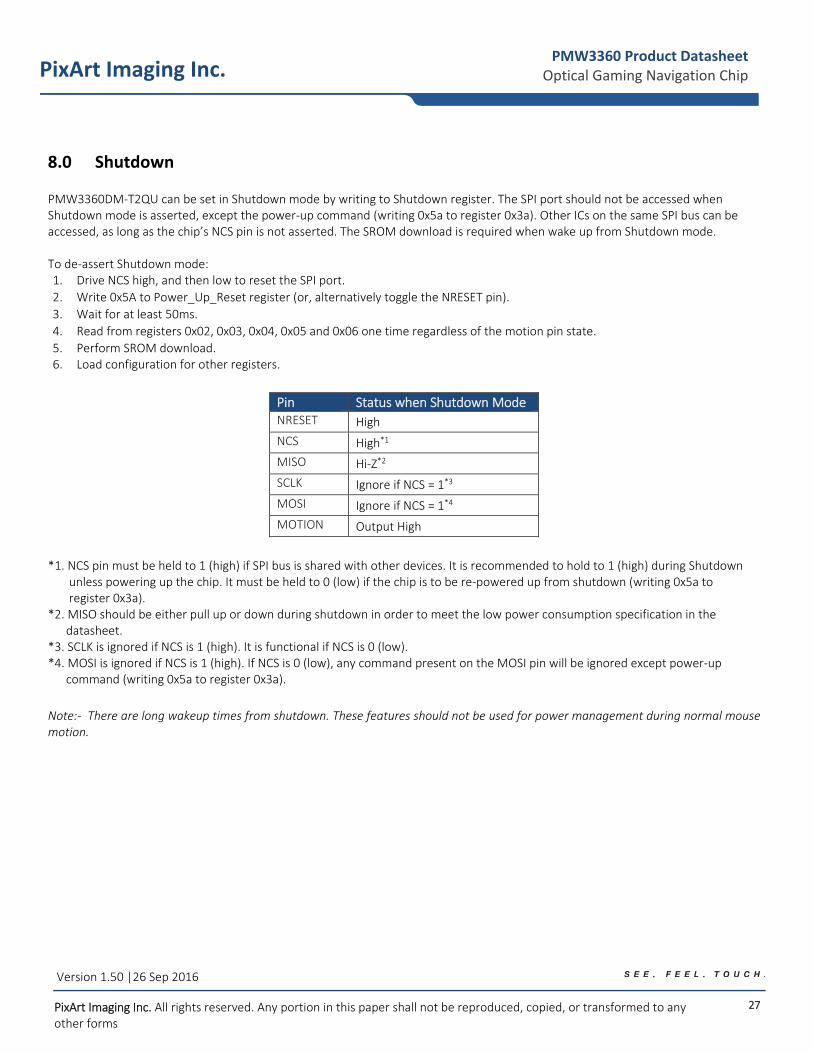
8.0 Shutdown PMW3360DM‐T2QU can be set in Shutdown mode by writing to Shutdown register. The SPI port should not be accessed when Shutdown mode is asserted, except the power‐up command (writing 0x5a to register 0x3a). Other ICs on the same SPI bus can be accessed, as long as the chip’s NCS pin is not asserted. The SROM download is required when wake up from Shutdown mode. To de‐assert Shutdown mode: 1. Drive NCS high, and then low to reset the SPI port.
2. Write 0x5A to Power_Up_Reset register (or, alternatively toggle the NRESET pin).
3. Wait for at least 50ms.
4. Read from registers 0x02, 0x03, 0x04, 0x05 and 0x06 one time regardless of the motion pin state.
5. Perform SROM download. 6. Load configuration for other registers.
*1. NCS pin must be held to 1 (high) if SPI bus is shared with other devices. It is recommended to hold to 1 (high) during Shutdown unless powering up the chip. It must be held to 0 (low) if the chip is to be re‐powered up from shutdown (writing 0x5a to register 0x3a). *2. MISO should be either pull up or down during shutdown in order to meet the low power consumption specification in the datasheet. *3. SCLK is ignored if NCS is 1 (high). It is functional if NCS is 0 (low). *4. MOSI is ignored if NCS is 1 (high). If NCS is 0 (low), any command present on the MOSI pin will be ignored except power‐up command (writing 0x5a to register 0x3a).
Note:‐ There are long wakeup times from shutdown. These features should not be used for power management during normal mouse motion.
Pin Status when Shutdown Mode NRESET High
NCS High*1
MISO Hi‐Z*2
SCLK Ignore if NCS = 1*3
MOSI Ignore if NCS = 1*4
MOTION Output High
28
PixArt Imaging Inc. PMW3360 Product Datasheet
Optical Gaming Navigation Chip
Version 1.50 |26 Sep 2016
PixArt Imaging Inc. All rights reserved. Any portion in this paper shall not be reproduced, copied, or transformed to any other forms
9.0 Lift cut off calibration This chip has the capability to optimize its lift performance by tuning internal parameters to the surface. This “Lift cut off calibration” feature involves user interaction. Take note that the Lift cut off calibration procedure that follows references registers of seven Lift cut off calibration related registers: (i) LiftCutoff_Tune1, (ii) LiftCutoff_Tune2, (iii) LiftCutoff_Tune3, (iv) LiftCutoff_Tune_Timeout, (v) LiftCutoff_Tune_Min_Length, (vi) Raw data_Threshold and (vii) Min_SQ_Run.
1. Ensure that the chip is powered up according to the Power Up Sequence.
2. Ensure that Lift cut off calibration SROM*1 is downloaded.
3. Delay for 30ms.
4. Prompt the user that the "Lift cut off calibration" procedure is about to begin to ensure that the mouse is placed nominally
on the surface (mouse is not lifted).
5. Start the calibration procedure by setting RUN_CAL register bit to 1. The calibration procedure can be started by a SW
prompt to the user or user‐initiated through a mouse‐click event.
6. Poll CAL_STAT[2:0] to check the status of the calibration procedure. There are three ways to successfully stop the
calibration procedure: set RUN_CAL register bit to 0 if either:
o CAL_STAT[2:0] = 0x02,
o CAL_STAT[2:0] = 0x02 and user initiates a stop through a mouse‐click event, or,
o CAL_STAT[2:0] = 0x03.
If CAL_STAT[2:0] = 0x04, the calibration procedure needs to be re‐started. 7. Stop the calibration procedure by ensuring that the RUN_CAL register bit is 0, then wait 1msec before reading the
recommended “Raw data Threshold” register value, RPTH[6:0] (lower 7 bits of LiftCutoff_Tune2 register). RPTH[6:0]
recommends a raw data threshold value that replaces the default value in the tracking SROM’s Raw_data_Threshold
register to improve lift performance. The Raw_ data_Threshold register requires the Tracking SROM*2 to be loaded.
8. Read the recommended “Min SQUAL Run” register value, RMSQ[7:0] (entire 8 bits of LiftCutoff_Tune3 register). RMSQ[7:0]
recommends a Min SQUAL Run value that replaces the default value in the tracking SROM’s Min_SQ_Run register to
improve lift performance. The Min_SQ_Run register requires the Tracking SROM*2 to be downloaded.
9. The Lift cut off calibration procedure is complete.
Note: *1 Lift cut off calibration SROM: SROM 0x81 or above (4KB). *2 Tracking SROM: SROM 0x03 or above (4KB).
29
PixArt Imaging Inc. PMW3360 Product Datasheet
Optical Gaming Navigation Chip
Version 1.50 |26 Sep 2016
PixArt Imaging Inc. All rights reserved. Any portion in this paper shall not be reproduced, copied, or transformed to any other forms
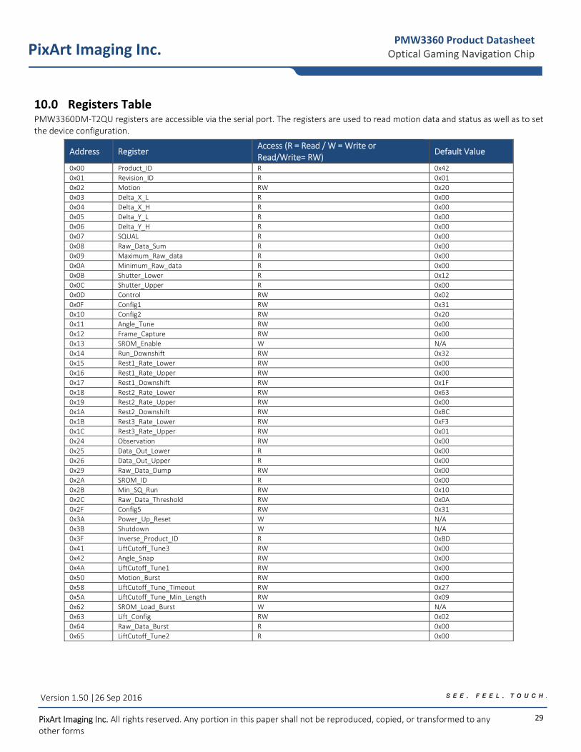
10.0 Registers Table PMW3360DM‐T2QU registers are accessible via the serial port. The registers are used to read motion data and status as well as to set the device configuration.
Address Register Access (R = Read / W = Write or Read/Write= RW)
Default Value
0x00 Product_ID R 0x42
0x01 Revision_ID R 0x01
0x02 Motion RW 0x20
0x03 Delta_X_L R 0x00
0x04 Delta_X_H R 0x00
0x05 Delta_Y_L R 0x00
0x06 Delta_Y_H R 0x00
0x07 SQUAL R 0x00
0x08 Raw_Data_Sum R 0x00
0x09 Maximum_Raw_data R 0x00
0x0A Minimum_Raw_data R 0x00
0x0B Shutter_Lower R 0x12
0x0C Shutter_Upper R 0x00
0x0D Control RW 0x02
0x0F Config1 RW 0x31
0x10 Config2 RW 0x20
0x11 Angle_Tune RW 0x00
0x12 Frame_Capture RW 0x00
0x13 SROM_Enable W N/A
0x14 Run_Downshift RW 0x32
0x15 Rest1_Rate_Lower RW 0x00
0x16 Rest1_Rate_Upper RW 0x00
0x17 Rest1_Downshift RW 0x1F
0x18 Rest2_Rate_Lower RW 0x63
0x19 Rest2_Rate_Upper RW 0x00
0x1A Rest2_Downshift RW 0xBC
0x1B Rest3_Rate_Lower RW 0xF3
0x1C Rest3_Rate_Upper RW 0x01
0x24 Observation RW 0x00
0x25 Data_Out_Lower R 0x00
0x26 Data_Out_Upper R 0x00
0x29 Raw_Data_Dump RW 0x00
0x2A SROM_ID R 0x00
0x2B Min_SQ_Run RW 0x10
0x2C Raw_Data_Threshold RW 0x0A
0x2F Config5 RW 0x31
0x3A Power_Up_Reset W N/A
0x3B Shutdown W N/A
0x3F Inverse_Product_ID R 0xBD
0x41 LiftCutoff_Tune3 RW 0x00
0x42 Angle_Snap RW 0x00
0x4A LiftCutoff_Tune1 RW 0x00
0x50 Motion_Burst RW 0x00
0x58 LiftCutoff_Tune_Timeout RW 0x27
0x5A LiftCutoff_Tune_Min_Length RW 0x09
0x62 SROM_Load_Burst W N/A
0x63 Lift_Config RW 0x02
0x64 Raw_Data_Burst R 0x00
0x65 LiftCutoff_Tune2 R 0x00
30
PixArt Imaging Inc. PMW3360 Product Datasheet
Optical Gaming Navigation Chip
Version 1.50 |26 Sep 2016
PixArt Imaging Inc. All rights reserved. Any portion in this paper shall not be reproduced, copied, or transformed to any other forms
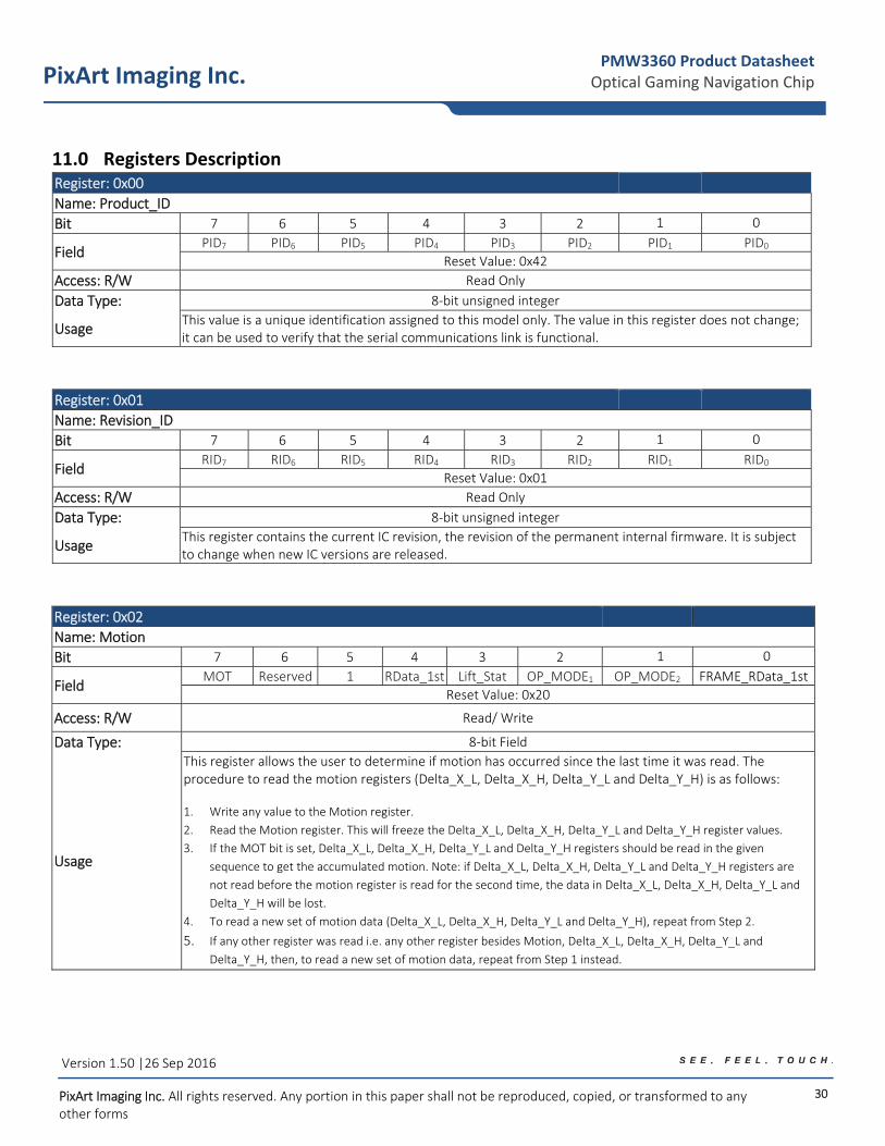
11.0 Registers Description Register: 0x00
Name: Product_ID
Bit 7 6 5 4 3 2 1 0
Field PID7 PID6 PID5 PID4 PID3 PID2 PID1 PID0
Reset Value: 0x42
Access: R/W Read Only
Data Type: 8‐bit unsigned integer
Usage This value is a unique identification assigned to this model only. The value in this register does not change; it can be used to verify that the serial communications link is functional.
Register: 0x01
Name: Revision_ID
Bit 7 6 5 4 3 2 1 0
Field RID7 RID6 RID5 RID4 RID3 RID2 RID1 RID0
Reset Value: 0x01
Access: R/W Read Only
Data Type: 8‐bit unsigned integer
Usage This register contains the current IC revision, the revision of the permanent internal firmware. It is subject to change when new IC versions are released.
Register: 0x02
Name: Motion
Bit 7 6 5 4 3 2 1 0
Field MOT Reserved 1 RData_1st Lift_Stat OP_MODE1 OP_MODE2 FRAME_RData_1st
Reset Value: 0x20
Access: R/W Read/ Write
Data Type: 8‐bit Field
Usage
This register allows the user to determine if motion has occurred since the last time it was read. The procedure to read the motion registers (Delta_X_L, Delta_X_H, Delta_Y_L and Delta_Y_H) is as follows: 1. Write any value to the Motion register.
2. Read the Motion register. This will freeze the Delta_X_L, Delta_X_H, Delta_Y_L and Delta_Y_H register values.
3. If the MOT bit is set, Delta_X_L, Delta_X_H, Delta_Y_L and Delta_Y_H registers should be read in the given
sequence to get the accumulated motion. Note: if Delta_X_L, Delta_X_H, Delta_Y_L and Delta_Y_H registers are
not read before the motion register is read for the second time, the data in Delta_X_L, Delta_X_H, Delta_Y_L and
Delta_Y_H will be lost.
4. To read a new set of motion data (Delta_X_L, Delta_X_H, Delta_Y_L and Delta_Y_H), repeat from Step 2.
5. If any other register was read i.e. any other register besides Motion, Delta_X_L, Delta_X_H, Delta_Y_L and
Delta_Y_H, then, to read a new set of motion data, repeat from Step 1 instead.
31
PixArt Imaging Inc. PMW3360 Product Datasheet
Optical Gaming Navigation Chip
Version 1.50 |26 Sep 2016
PixArt Imaging Inc. All rights reserved. Any portion in this paper shall not be reproduced, copied, or transformed to any other forms
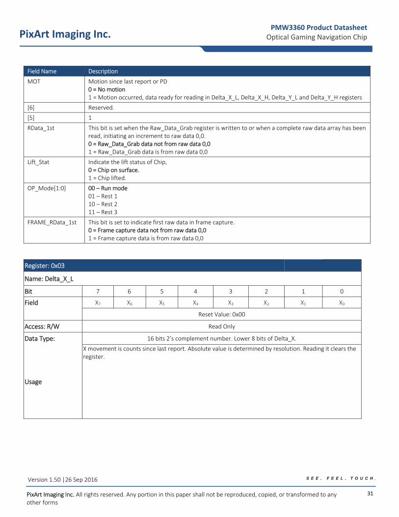
Field Name Description
MOT Motion since last report or PD0 = No motion 1 = Motion occurred, data ready for reading in Delta_X_L, Delta_X_H, Delta_Y_L and Delta_Y_H registers
[6] Reserved.
[5] 1
RData_1st This bit is set when the Raw_Data_Grab register is written to or when a complete raw data array has been read, initiating an increment to raw data 0,0. 0 = Raw_Data_Grab data not from raw data 0,0 1 = Raw_Data_Grab data is from raw data 0,0
Lift_Stat Indicate the lift status of Chip,0 = Chip on surface. 1 = Chip lifted.
OP_Mode[1:0] 00 – Run mode 01 – Rest 1 10 – Rest 2 11 – Rest 3
FRAME_RData_1st This bit is set to indicate first raw data in frame capture.0 = Frame capture data not from raw data 0,0 1 = Frame capture data is from raw data 0,0
Register: 0x03
Name: Delta_X_L
Bit 7 6 5 4 3 2 1 0
Field X7 X6 X5 X4 X3 X2 X1 X0
Reset Value: 0x00
Access: R/W Read Only
Data Type: 16 bits 2’s complement number. Lower 8 bits of Delta_X.
Usage
X movement is counts since last report. Absolute value is determined by resolution. Reading it clears the register.
32
PixArt Imaging Inc. PMW3360 Product Datasheet
Optical Gaming Navigation Chip
Version 1.50 |26 Sep 2016
PixArt Imaging Inc. All rights reserved. Any portion in this paper shall not be reproduced, copied, or transformed to any other forms
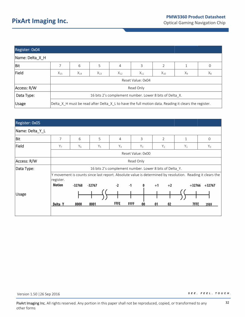
Register: 0x04
Name: Delta_X_H
Bit 7 6 5 4 3 2 1 0
Field X15 X14 X13 X12 X11 X10 X9 X8
Reset Value: 0x04
Access: R/W Read Only
Data Type: 16 bits 2’s complement number. Lower 8 bits of Delta_X.
Usage Delta_X_H must be read after Delta_X_L to have the full motion data. Reading it clears the register.
Register: 0x05
Name: Delta_Y_L
Bit 7 6 5 4 3 2 1 0
Field Y7 Y6 Y5 Y4 Y3 Y2 Y1 Y0
Reset Value: 0x00
Access: R/W Read Only
Data Type: 16 bits 2’s complement number. Lower 8 bits of Delta_Y.
Usage
Y movement is counts since last report. Absolute value is determined by resolution. Reading it clears the register.
33
PixArt Imaging Inc. PMW3360 Product Datasheet
Optical Gaming Navigation Chip
Version 1.50 |26 Sep 2016
PixArt Imaging Inc. All rights reserved. Any portion in this paper shall not be reproduced, copied, or transformed to any other forms
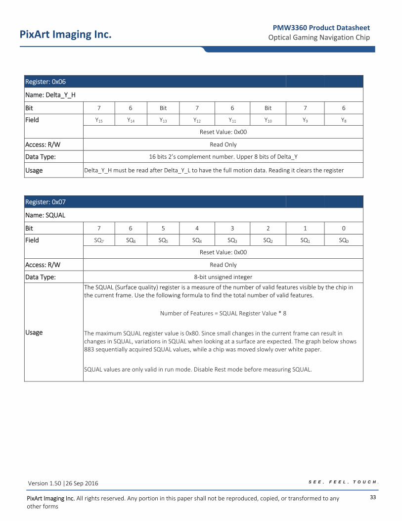
Register: 0x06
Name: Delta_Y_H
Bit 7 6 Bit 7 6 Bit 7 6
Field Y15 Y14 Y13 Y12 Y11 Y10 Y9 Y8
Reset Value: 0x00
Access: R/W Read Only
Data Type: 16 bits 2’s complement number. Upper 8 bits of Delta_Y
Usage Delta_Y_H must be read after Delta_Y_L to have the full motion data. Reading it clears the register
Register: 0x07
Name: SQUAL
Bit 7 6 5 4 3 2 1 0
Field SQ7 SQ6 SQ5 SQ4 SQ3 SQ2 SQ1 SQ0
Reset Value: 0x00
Access: R/W Read Only
Data Type: 8‐bit unsigned integer
Usage
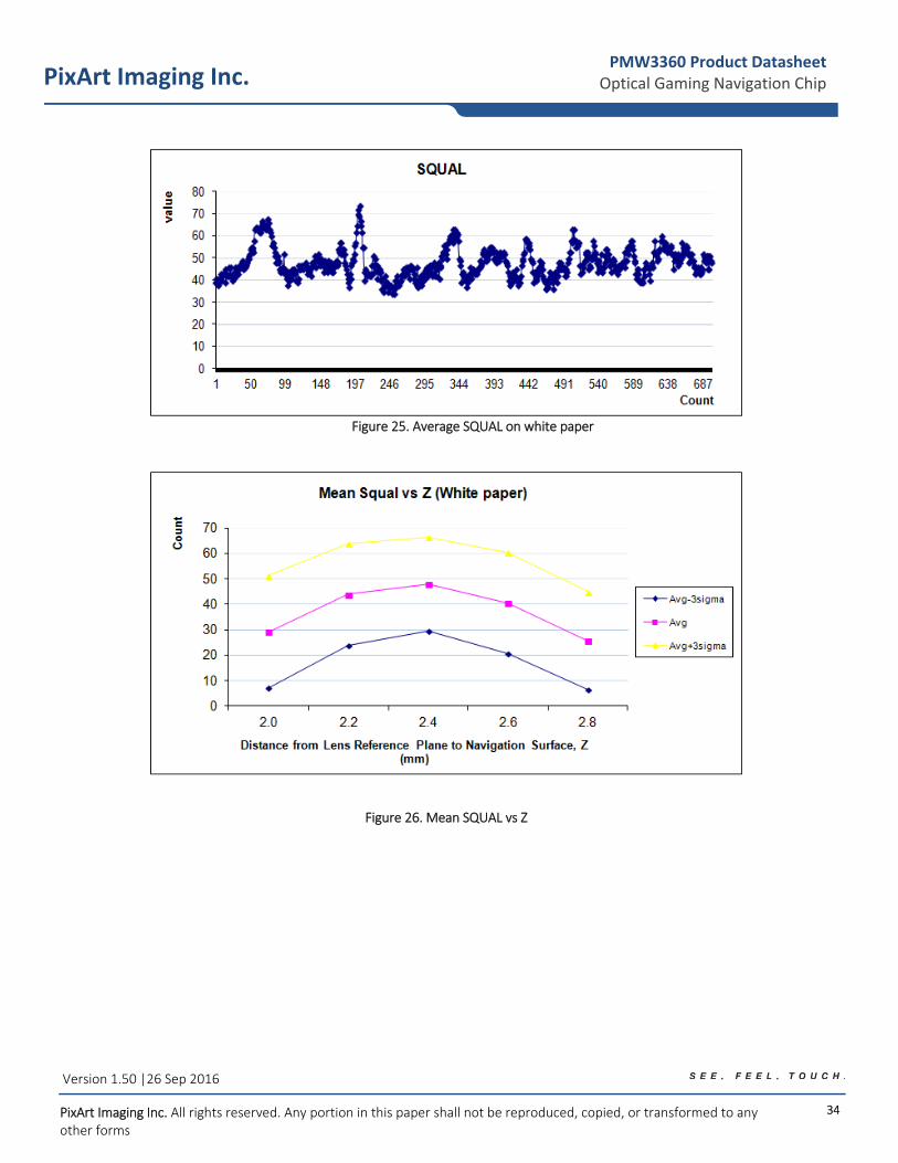
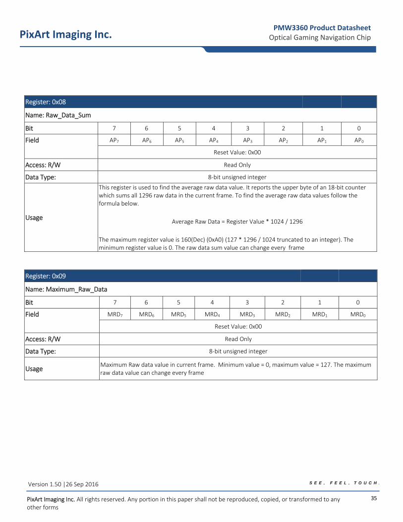
The SQUAL (Surface quality) register is a measure of the number of valid features visible by the chip in the current frame. Use the following formula to find the total number of valid features.
Number of Features = SQUAL Register Value * 8
The maximum SQUAL register value is 0x80. Since small changes in the current frame can result in changes in SQUAL, variations in SQUAL when looking at a surface are expected. The graph below shows 883 sequentially acquired SQUAL values, while a chip was moved slowly over white paper.
SQUAL values are only valid in run mode. Disable Rest mode before measuring SQUAL.
34
PixArt Imaging Inc. PMW3360 Product Datasheet
Optical Gaming Navigation Chip
Version 1.50 |26 Sep 2016
PixArt Imaging Inc. All rights reserved. Any portion in this paper shall not be reproduced, copied, or transformed to any other forms
Figure 25. Average SQUAL on white paper
Figure 26. Mean SQUAL vs Z
35
PixArt Imaging Inc. PMW3360 Product Datasheet
Optical Gaming Navigation Chip
Version 1.50 |26 Sep 2016
PixArt Imaging Inc. All rights reserved. Any portion in this paper shall not be reproduced, copied, or transformed to any other forms
Register: 0x08
Name: Raw_Data_Sum
Bit 7 6 5 4 3 2 1 0
Field AP7 AP6 AP5 AP4 AP3 AP2 AP1 AP0
Reset Value: 0x00
Access: R/W Read Only
Data Type: 8‐bit unsigned integer
Usage
This register is used to find the average raw data value. It reports the upper byte of an 18‐bit counter which sums all 1296 raw data in the current frame. To find the average raw data values follow the formula below.
Average Raw Data = Register Value * 1024 / 1296
The maximum register value is 160(Dec) (0xA0) (127 * 1296 / 1024 truncated to an integer). The minimum register value is 0. The raw data sum value can change every frame
Register: 0x09
Name: Maximum_Raw_Data
Bit 7 6 5 4 3 2 1 0
Field MRD7 MRD6 MRD5 MRD4 MRD3 MRD2 MRD1 MRD0
Reset Value: 0x00
Access: R/W Read Only
Data Type: 8‐bit unsigned integer
Usage Maximum Raw data value in current frame. Minimum value = 0, maximum value = 127. The maximum raw data value can change every frame
36
PixArt Imaging Inc. PMW3360 Product Datasheet
Optical Gaming Navigation Chip
Version 1.50 |26 Sep 2016
PixArt Imaging Inc. All rights reserved. Any portion in this paper shall not be reproduced, copied, or transformed to any other forms
Register: 0x0A
Name: Minimum_Raw_Data
Bit 7 6 5 4 3 2 1 0
Field MinRD7 MinRD6 MinRD5 MinRD4 MinRD3 MinRD2 MinRD1 MinRD0
Reset Value: 0x00
Access: R/W Read Only
Data Type: 8‐bit unsigned integer
Usage Minimum Raw data value in current frame. Minimum value = 0, maximum value = 127. The minimum raw data value can change every frame
Register: 0x0B
Name: Shutter_Lower
Bit 7 6 5 4 3 2 1 0
Field S7 S 6 S 5 S 4 S 3 S 2 S 1 S 0
Reset Value: 0x12
Access: R/W Read Only
Data Type: 16‐bit unsigned number
Usage Lower byte of the 16bit Shutter register
Register: 0x0C
Name: Shutter_Upper
Bit 7 6 5 4 3 2 1 0
Field S15 S 14 S 13 S 12 S 11 S 10 S 9 S 8
Reset Value: 0x00
Access: R/W Read Only
Data Type: 16‐bit unsigned number
Usage
Units are clock cycles of the internal oscillator. Read Shutter_Upper first, then Shutter_Lower. They should be read consecutively. The shutter is adjusted to keep the average raw data values within normal operating ranges. The shutter value is checked and automatically adjusted to a new value if needed on every frame when operating in default mode.
37
PixArt Imaging Inc. PMW3360 Product Datasheet
Optical Gaming Navigation Chip
Version 1.50 |26 Sep 2016
PixArt Imaging Inc. All rights reserved. Any portion in this paper shall not be reproduced, copied, or transformed to any other forms
Register: 0x0D
Name: Control
Bit 7 6 5 4 3 2 1 0
Field CTRL17 CTRL16 CTRL15 Reserved Reserved Reserved Reserved Reserved
Reset Value: 0x02
Access: R/W Read Write
Data Type: 8‐bit unsigned integer
Usage
This register defines programmable invert able of XY register scheme.
Field Name Description
CTRL1[7:5] 000 ‐ 0 degree110 ‐ 90 degree 011 – 180 degree 101 – 270 degree
Reserved[4:0] Reserved
Note: For CTRL1[7:5] please use 0 degree for best performance
38
PixArt Imaging Inc. PMW3360 Product Datasheet
Optical Gaming Navigation Chip
Version 1.50 |26 Sep 2016
PixArt Imaging Inc. All rights reserved. Any portion in this paper shall not be reproduced, copied, or transformed to any other forms
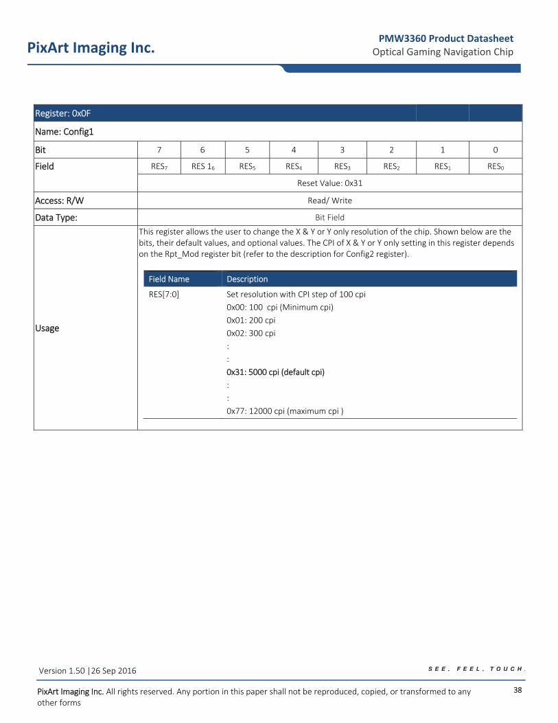
Register: 0x0F
Name: Config1
Bit 7 6 5 4 3 2 1 0
Field RES7 RES 16 RES5 RES4 RES3 RES2 RES1 RES0
Reset Value: 0x31
Access: R/W Read/ Write
Data Type: Bit Field
Usage
This register allows the user to change the X & Y or Y only resolution of the chip. Shown below are the bits, their default values, and optional values. The CPI of X & Y or Y only setting in this register depends on the Rpt_Mod register bit (refer to the description for Config2 register).
Field Name Description
RES[7:0] Set resolution with CPI step of 100 cpi
0x00: 100 cpi (Minimum cpi)
0x01: 200 cpi
0x02: 300 cpi
:
:
0x31: 5000 cpi (default cpi)
:
:
0x77: 12000 cpi (maximum cpi )
39
PixArt Imaging Inc. PMW3360 Product Datasheet
Optical Gaming Navigation Chip
Version 1.50 |26 Sep 2016
PixArt Imaging Inc. All rights reserved. Any portion in this paper shall not be reproduced, copied, or transformed to any other forms
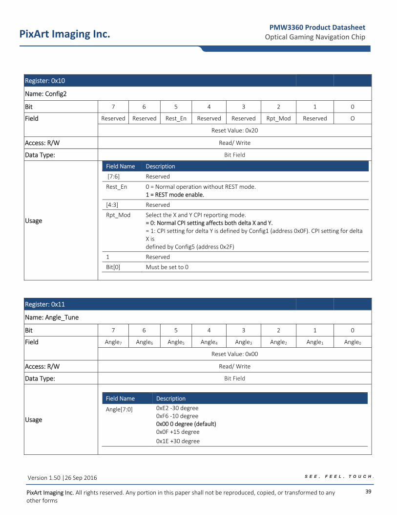
Register: 0x10
Name: Config2
Bit 7 6 5 4 3 2 1 0
Field Reserved Reserved Rest_En Reserved Reserved Rpt_Mod Reserved O
Reset Value: 0x20
Access: R/W Read/ Write
Data Type: Bit Field
Usage
Field Name Description
[7:6] Reserved
Rest_En 0 = Normal operation without REST mode.1 = REST mode enable.
[4:3] Reserved
Rpt_Mod Select the X and Y CPI reporting mode.= 0: Normal CPI setting affects both delta X and Y. = 1: CPI setting for delta Y is defined by Config1 (address 0x0F). CPI setting for delta X is defined by Config5 (address 0x2F)
1 Reserved
Bit[0] Must be set to 0
Register: 0x11
Name: Angle_Tune
Bit 7 6 5 4 3 2 1 0
Field Angle7 Angle6 Angle5 Angle4 Angle3 Angle2 Angle1 Angle0
Reset Value: 0x00
Access: R/W Read/ Write
Data Type: Bit Field
Usage
Field Name Description
Angle[7:0] 0xE2 ‐30 degree0xF6 ‐10 degree 0x00 0 degree (default) 0x0F +15 degree
0x1E +30 degree
40
PixArt Imaging Inc. PMW3360 Product Datasheet
Optical Gaming Navigation Chip
Version 1.50 |26 Sep 2016
PixArt Imaging Inc. All rights reserved. Any portion in this paper shall not be reproduced, copied, or transformed to any other forms
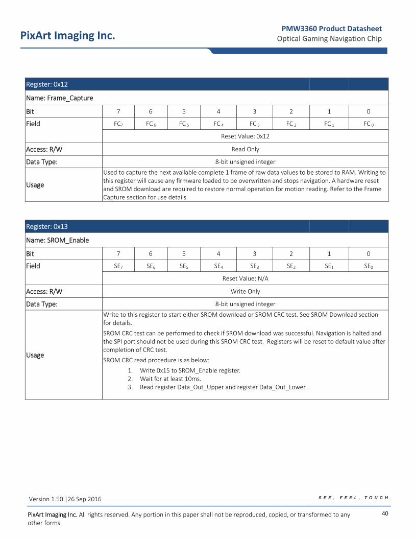
Register: 0x12
Name: Frame_Capture
Bit 7 6 5 4 3 2 1 0
Field FC7 FC 6 FC 5 FC 4 FC 3 FC 2 FC 1 FC 0
Reset Value: 0x12
Access: R/W Read Only
Data Type: 8‐bit unsigned integer
Usage
Used to capture the next available complete 1 frame of raw data values to be stored to RAM. Writing to this register will cause any firmware loaded to be overwritten and stops navigation. A hardware reset and SROM download are required to restore normal operation for motion reading. Refer to the Frame Capture section for use details.
Register: 0x13
Name: SROM_Enable
Bit 7 6 5 4 3 2 1 0
Field SE7 SE6 SE5 SE4 SE3 SE2 SE1 SE0
Reset Value: N/A
Access: R/W Write Only
Data Type: 8‐bit unsigned integer
Usage
Write to this register to start either SROM download or SROM CRC test. See SROM Download section for details.
SROM CRC test can be performed to check if SROM download was successful. Navigation is halted and the SPI port should not be used during this SROM CRC test. Registers will be reset to default value after completion of CRC test.
SROM CRC read procedure is as below:
1. Write 0x15 to SROM_Enable register. 2. Wait for at least 10ms. 3. Read register Data_Out_Upper and register Data_Out_Lower .
41
PixArt Imaging Inc. PMW3360 Product Datasheet
Optical Gaming Navigation Chip
Version 1.50 |26 Sep 2016
PixArt Imaging Inc. All rights reserved. Any portion in this paper shall not be reproduced, copied, or transformed to any other forms
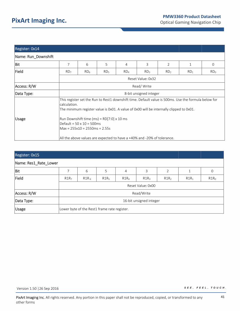
Register: 0x14
Name: Run_Downshift
Bit 7 6 5 4 3 2 1 0
Field RD7 RD6 RD5 RD4 RD3 RD2 RD1 RD0
Reset Value: 0x32
Access: R/W Read/ Write
Data Type: 8‐bit unsigned integer
Usage
This register set the Run to Rest1 downshift time. Default value is 500ms. Use the formula below for calculation. The minimum register value is 0x01. A value of 0x00 will be internally clipped to 0x01. Run Downshift time (ms) = RD[7:0] x 10 ms Default = 50 x 10 = 500ms Max = 255x10 = 2550ms = 2.55s All the above values are expected to have a +40% and ‐20% of tolerance.
Register: 0x15
Name: Res1_Rate_Lower
Bit 7 6 5 4 3 2 1 0
Field R1R7 R1R 6 R1R5 R1R4 R1R3 R1R2 R1R1 R1R0
Reset Value: 0x00
Access: R/W Read/Write
Data Type: 16‐bit unsigned integer
Usage Lower byte of the Rest1 frame rate register.
42
PixArt Imaging Inc. PMW3360 Product Datasheet
Optical Gaming Navigation Chip
Version 1.50 |26 Sep 2016
PixArt Imaging Inc. All rights reserved. Any portion in this paper shall not be reproduced, copied, or transformed to any other forms
Register: 0x16
Name: Rest1_Rate_Upper
Bit 7 6 5 4 3 2 1 0
Field R1R15 R1R14 R1R13 R1R12 R1R11 R1R10 R1R9 R1R8
Reset Value: 0x00
Access: R/W Read/Write
Data Type: 16‐bit unsigned integer
Usage
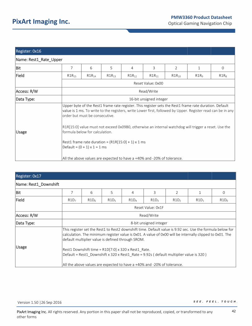
Upper byte of the Rest1 frame rate register. This register sets the Rest1 frame rate duration. Default value is 1 ms. To write to the registers, write Lower first, followed by Upper. Register read can be in any order but must be consecutive.
R1R[15:0] value must not exceed 0x09B0, otherwise an internal watchdog will trigger a reset. Use the formula below for calculation. Rest1 frame rate duration = (R1R[15:0] + 1) x 1 ms Default = (0 + 1) x 1 = 1 ms
All the above values are expected to have a +40% and ‐20% of tolerance.
Register: 0x17
Name: Rest1_Downshift
Bit 7 6 5 4 3 2 1 0
Field R1D7 R1D6 R1D5 R1D4 R1D3 R1D2 R1D1 R1D0
Reset Value: 0x1F
Access: R/W Read/Write
Data Type: 8‐bit unsigned integer
Usage
This register set the Rest1 to Rest2 downshift time. Default value is 9.92 sec. Use the formula below for calculation. The minimum register value is 0x01. A value of 0x00 will be internally clipped to 0x01. The default multiplier value is defined through SROM. Rest1 Downshift time = R1D[7:0] x 320 x Rest1_Rate. Default = Rest1_Downshift x 320 x Rest1_Rate = 9.92s ( default multiplier value is 320 )
All the above values are expected to have a +40% and ‐20% of tolerance.
43
PixArt Imaging Inc. PMW3360 Product Datasheet
Optical Gaming Navigation Chip
Version 1.50 |26 Sep 2016
PixArt Imaging Inc. All rights reserved. Any portion in this paper shall not be reproduced, copied, or transformed to any other forms
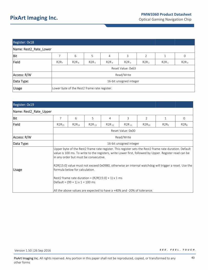
Register: 0x18
Name: Rest2_Rate_Lower
Bit 7 6 5 4 3 2 1 0
Field R2R7 R2R 6 R2R 5 R2R 4 R2R 3 R2R 2 R2R 1 R2R 0
Reset Value: 0x63
Access: R/W Read/Write
Data Type: 16‐bit unsigned integer
Usage Lower byte of the Rest2 frame rate register.
Register: 0x19
Name: Rest2_Rate_Upper
Bit 7 6 5 4 3 2 1 0
Field R2R15 R2R14 R2R 13 R2R 12 R2R 11 R2R10 R2R9 R2R8
Reset Value: 0x00
Access: R/W Read/Write
Data Type: 16‐bit unsigned integer
Usage
Upper byte of the Rest2 frame rate register. This register sets the Rest2 frame rate duration. Default value is 100 ms. To write to the registers, write Lower first, followed by Upper. Register read can be in any order but must be consecutive. R2R[15:0] value must not exceed 0x09B0, otherwise an internal watchdog will trigger a reset. Use the formula below for calculation. Rest2 frame rate duration = (R2R[15:0] + 1) x 1 ms Default = (99 + 1) x 1 = 100 ms All the above values are expected to have a +40% and ‐20% of tolerance.
44
PixArt Imaging Inc. PMW3360 Product Datasheet
Optical Gaming Navigation Chip
Version 1.50 |26 Sep 2016
PixArt Imaging Inc. All rights reserved. Any portion in this paper shall not be reproduced, copied, or transformed to any other forms
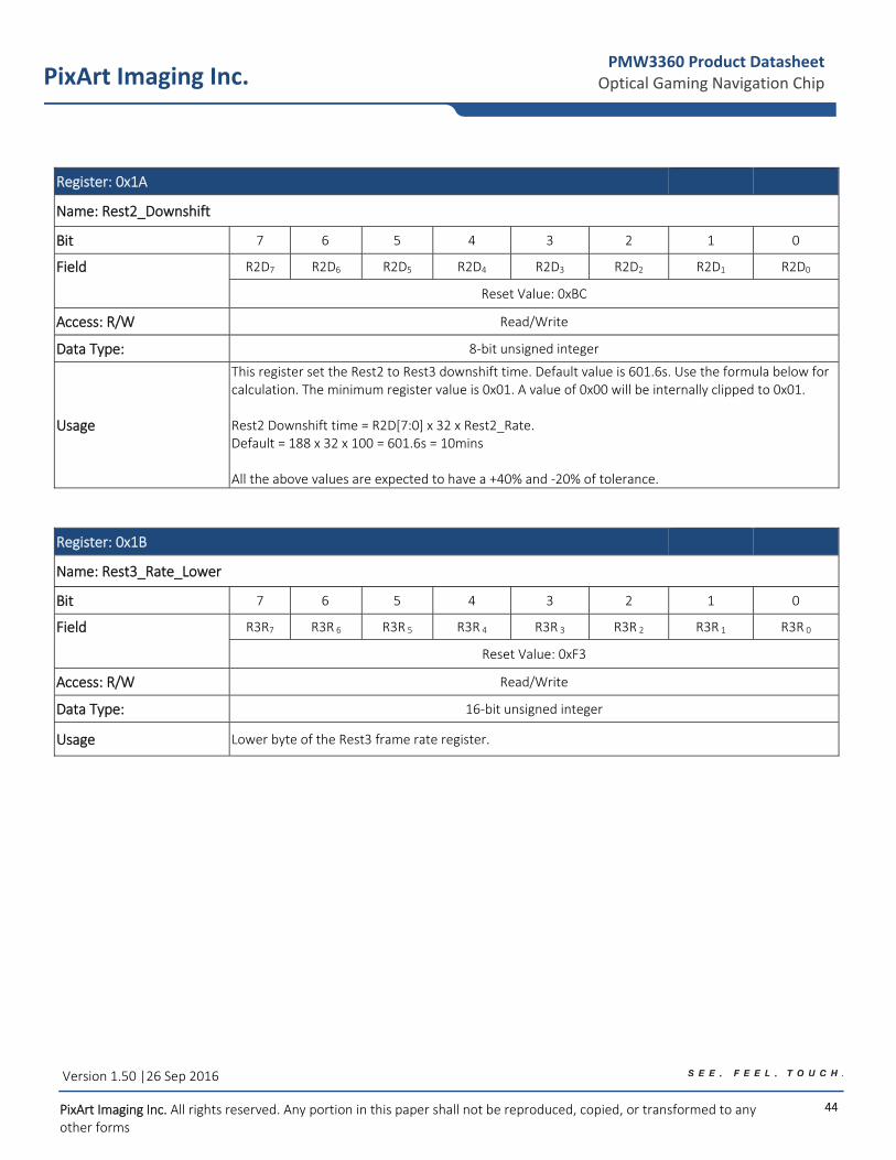
Register: 0x1A
Name: Rest2_Downshift
Bit 7 6 5 4 3 2 1 0
Field R2D7 R2D6 R2D5 R2D4 R2D3 R2D2 R2D1 R2D0
Reset Value: 0xBC
Access: R/W Read/Write
Data Type: 8‐bit unsigned integer
Usage
This register set the Rest2 to Rest3 downshift time. Default value is 601.6s. Use the formula below for calculation. The minimum register value is 0x01. A value of 0x00 will be internally clipped to 0x01. Rest2 Downshift time = R2D[7:0] x 32 x Rest2_Rate. Default = 188 x 32 x 100 = 601.6s = 10mins All the above values are expected to have a +40% and ‐20% of tolerance.
Register: 0x1B
Name: Rest3_Rate_Lower
Bit 7 6 5 4 3 2 1 0
Field R3R7 R3R 6 R3R 5 R3R 4 R3R 3 R3R 2 R3R 1 R3R 0
Reset Value: 0xF3
Access: R/W Read/Write
Data Type: 16‐bit unsigned integer
Usage Lower byte of the Rest3 frame rate register.
45
PixArt Imaging Inc. PMW3360 Product Datasheet
Optical Gaming Navigation Chip
Version 1.50 |26 Sep 2016
PixArt Imaging Inc. All rights reserved. Any portion in this paper shall not be reproduced, copied, or transformed to any other forms
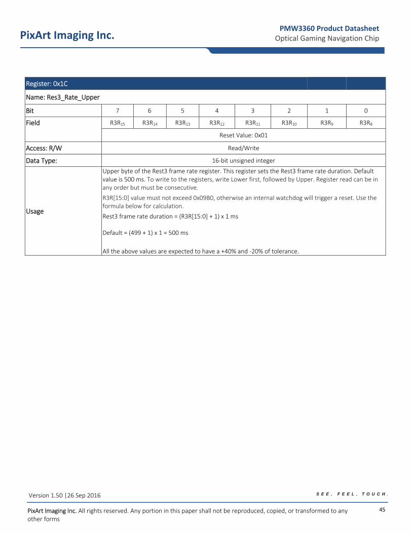
Register: 0x1C
Name: Res3_Rate_Upper
Bit 7 6 5 4 3 2 1 0
Field R3R15 R3R14 R3R13 R3R12 R3R11 R3R10 R3R9 R3R8
Reset Value: 0x01
Access: R/W Read/Write
Data Type: 16‐bit unsigned integer
Usage
Upper byte of the Rest3 frame rate register. This register sets the Rest3 frame rate duration. Default value is 500 ms. To write to the registers, write Lower first, followed by Upper. Register read can be in any order but must be consecutive.
R3R[15:0] value must not exceed 0x09B0, otherwise an internal watchdog will trigger a reset. Use the formula below for calculation.
Rest3 frame rate duration = (R3R[15:0] + 1) x 1 ms Default = (499 + 1) x 1 = 500 ms
All the above values are expected to have a +40% and ‐20% of tolerance.
46
PixArt Imaging Inc. PMW3360 Product Datasheet
Optical Gaming Navigation Chip
Version 1.50 |26 Sep 2016
PixArt Imaging Inc. All rights reserved. Any portion in this paper shall not be reproduced, copied, or transformed to any other forms
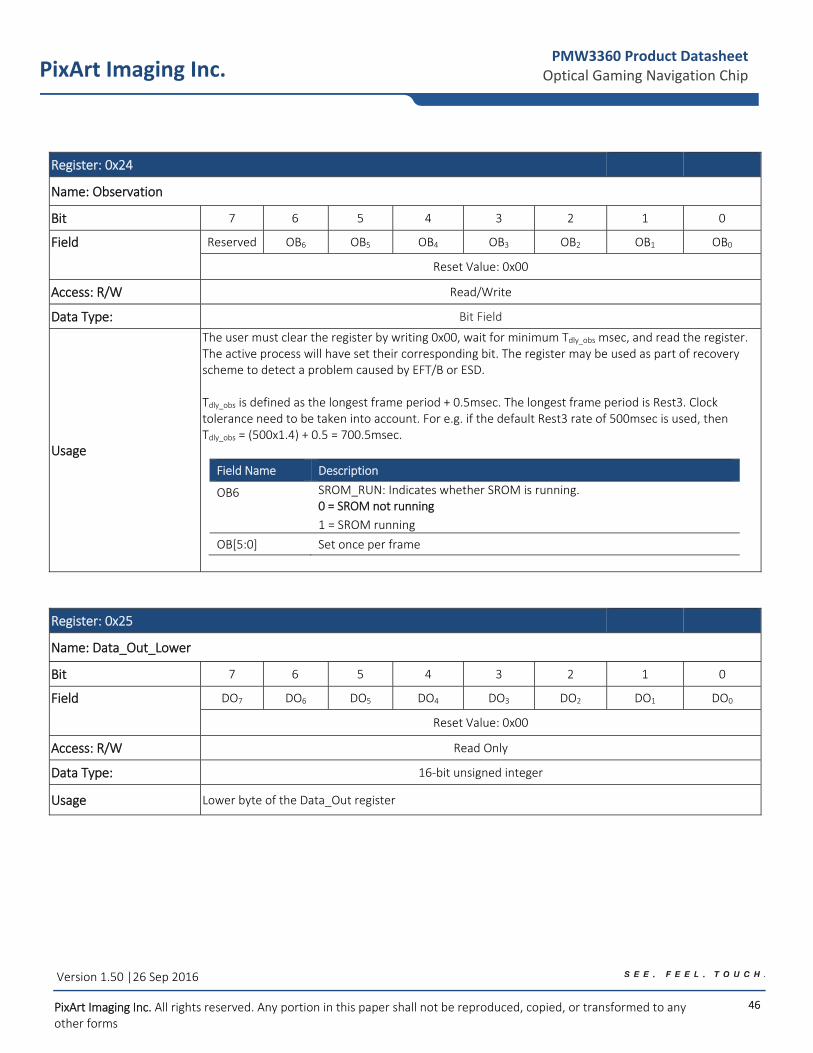
Register: 0x24
Name: Observation
Bit 7 6 5 4 3 2 1 0
Field Reserved OB6 OB5 OB4 OB3 OB2 OB1 OB0
Reset Value: 0x00
Access: R/W Read/Write
Data Type: Bit Field
Usage
The user must clear the register by writing 0x00, wait for minimum Tdly_obs msec, and read the register. The active process will have set their corresponding bit. The register may be used as part of recovery scheme to detect a problem caused by EFT/B or ESD. Tdly_obs is defined as the longest frame period + 0.5msec. The longest frame period is Rest3. Clock tolerance need to be taken into account. For e.g. if the default Rest3 rate of 500msec is used, then Tdly_obs = (500x1.4) + 0.5 = 700.5msec.
Field Name Description
OB6 SROM_RUN: Indicates whether SROM is running. 0 = SROM not running
1 = SROM running
OB[5:0] Set once per frame
Register: 0x25
Name: Data_Out_Lower
Bit 7 6 5 4 3 2 1 0
Field DO7 DO6 DO5 DO4 DO3 DO2 DO1 DO0
Reset Value: 0x00
Access: R/W Read Only
Data Type: 16‐bit unsigned integer
Usage Lower byte of the Data_Out register
47
PixArt Imaging Inc. PMW3360 Product Datasheet
Optical Gaming Navigation Chip
Version 1.50 |26 Sep 2016
PixArt Imaging Inc. All rights reserved. Any portion in this paper shall not be reproduced, copied, or transformed to any other forms
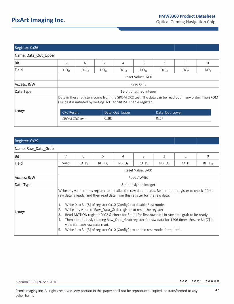
Register: 0x26
Name: Data_Out_Upper
Bit 7 6 5 4 3 2 1 0
Field DO15 DO14 DO13 DO12 DO11 DO10 DO9 DO8
Reset Value: 0x00
Access: R/W Read Only
Data Type: 16‐bit unsigned integer
Usage
Data in these registers come from the SROM CRC test. The data can be read out in any order. The SROM CRC test is initiated by writing 0x15 to SROM_Enable register.
CRC Result Data_Out_Upper Data_Out_Lower
SROM CRC test 0xBE 0xEF
Register: 0x29
Name: Raw_Data_Grab
Bit 7 6 5 4 3 2 1 0
Field Valid RD_D6 RD_D5 RD_D4 RD_D3 RD_D2 RD_D1 RD_D0
Reset Value: 0x00
Access: R/W Read / Write
Data Type: 8‐bit unsigned integer
Usage
Write any value to this register to initialize the raw data output. Read motion register to check if first raw data is ready, and then read data from this register for the raw data. 1. Write 0 to Bit [5] of register 0x10 (Config2) to disable Rest mode.
2. Write any value to Raw_Data_Grab register to reset the register.
3. Read MOTION register 0x02 & check for Bit [4] for first raw data in raw data grab to be ready.
4. Then continuously reading Raw_Data_Grab register for raw data for 1296 times. Ensure Bit [7] is
valid for each raw data read.
5. Write 1 to Bit [5] of register 0x10 (Config2) to enable rest mode if required.
48
PixArt Imaging Inc. PMW3360 Product Datasheet
Optical Gaming Navigation Chip
Version 1.50 |26 Sep 2016
PixArt Imaging Inc. All rights reserved. Any portion in this paper shall not be reproduced, copied, or transformed to any other forms
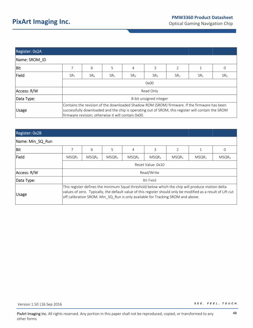
Register: 0x2A
Name: SROM_ID
Bit 7 6 5 4 3 2 1 0
Field SR7 SR6 SR5 SR4 SR3 SR2 SR1 SR0
0x00
Access: R/W Read Only
Data Type: 8‐bit unsigned integer
Usage Contains the revision of the downloaded Shadow ROM (SROM) firmware. If the firmware has been successfully downloaded and the chip is operating out of SROM, this register will contain the SROM firmware revision; otherwise it will contain 0x00.
Register: 0x2B
Name: Min_SQ_Run
Bit 7 6 5 4 3 2 1 0
Field MSQR7 MSQR6 MSQR5 MSQR4 MSQR3 MSQR2 MSQR1 MSQR0
Reset Value: 0x10
Access: R/W Read/Write
Data Type: Bit Field
Usage
This register defines the minimum Squal threshold below which the chip will produce motion delta values of zero. Typically, the default value of this register should only be modified as a result of Lift cut off calibration SROM. Min_SQ_Run is only available for Tracking SROM and above.
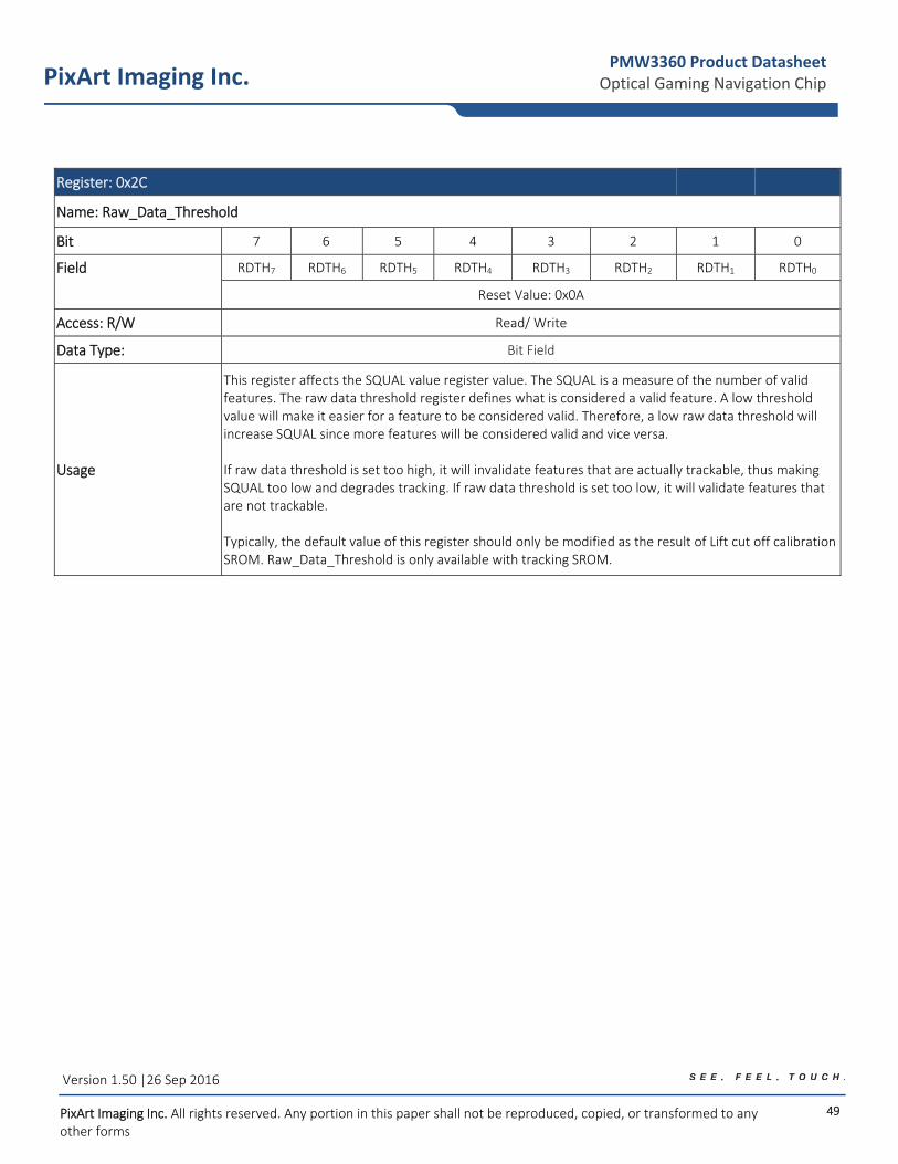
49
PixArt Imaging Inc. PMW3360 Product Datasheet
Optical Gaming Navigation Chip
Version 1.50 |26 Sep 2016
PixArt Imaging Inc. All rights reserved. Any portion in this paper shall not be reproduced, copied, or transformed to any other forms
Register: 0x2C
Name: Raw_Data_Threshold
Bit 7 6 5 4 3 2 1 0
Field RDTH7 RDTH6 RDTH5 RDTH4 RDTH3 RDTH2 RDTH1 RDTH0
Reset Value: 0x0A
Access: R/W Read/ Write
Data Type: Bit Field
Usage
This register affects the SQUAL value register value. The SQUAL is a measure of the number of valid features. The raw data threshold register defines what is considered a valid feature. A low threshold value will make it easier for a feature to be considered valid. Therefore, a low raw data threshold will increase SQUAL since more features will be considered valid and vice versa. If raw data threshold is set too high, it will invalidate features that are actually trackable, thus making SQUAL too low and degrades tracking. If raw data threshold is set too low, it will validate features that are not trackable. Typically, the default value of this register should only be modified as the result of Lift cut off calibration SROM. Raw_Data_Threshold is only available with tracking SROM.
50
PixArt Imaging Inc. PMW3360 Product Datasheet
Optical Gaming Navigation Chip
Version 1.50 |26 Sep 2016
PixArt Imaging Inc. All rights reserved. Any portion in this paper shall not be reproduced, copied, or transformed to any other forms
Register: 0x2F
Name: Config5
Bit 7 6 5 4 3 2 1 0
Field RESX7 RESX6 RESX5 RESX4 RESX3 RESX2 RESX1 RESX0
Reset Value: 0x31
Access: R/W Read/ Write
Data Type: Bit Field
Usage
This register allows the user to change the X‐axis resolution when the chip is configured to have independent X‐axis and Y‐axis resolution reporting mode via Rpt_Mod bit = 1 in Config2 register. The setting in this register will be inactive if Rpt_Mod bit = 0.Shown below are the bits, their default values, and optional values.
Field Name Description
RESX [7:0] Set resolution with CPI step of 100 cpi
0x00: 100 cpi (Minimum cpi)
0x01: 200 cpi
0x02: 300 cpi
:
:
0x31: 5000 cpi (default cpi)
:
:
0x77: 12000 cpi (maximum cpi )
Register: 0x3A
Name: Power_Up_Reset
Bit 7 6 5 4 3 2 1 0
Field PUR7 PUR6 PUR5 PUR4 PUR3 PUR2 PUR1 PUR0
Reset Value: N/A
Access: R/W Write Only
Data Type: 8‐bit unsigned integer
Usage Write 0x5a to this register to reset the chip. All settings will revert to default values. Reset is required after recovering from shutdown mode and to restore normal operation after Frame Capture
51
PixArt Imaging Inc. PMW3360 Product Datasheet
Optical Gaming Navigation Chip
Version 1.50 |26 Sep 2016
PixArt Imaging Inc. All rights reserved. Any portion in this paper shall not be reproduced, copied, or transformed to any other forms
Register: 0x3B
Name: Shutdown
Bit 7 6 5 4 3 2 1 0
Field SD7 SD6 SD5 SD4 SD3 SD2 SD1 SD0
Reset Value: N/A
Access: R/W Write Only
Data Type: 8‐bit unsigned integer
Usage Write 0xB6 to set the chip to shutdown mode. Refer to the Shutdown section for more details and on the recovery procedure.
Register: 0x3F
Name: Inverse_Product_ID
Bit 7 6 5 4 3 2 1 0
Field PID7 PID6 PID5 PID4 PID3 PID2 PID1 PID0
Reset Value: 0xBD
Access: R/W Read Only
Data Type: Bit Field
Usage This value is the inverse of the Product_ID. It is used to test the SPI port hardware
Register: 0x41
Name: LiftCuttoff_Tune3
Bit 7 6 5 4 3 2 1 0
Field RMSQ7 RMSQ6 RMSQ5 RMSQ4 RMSQ3 RMSQ3 RMSQ1 RMSQ0
Reset Value: 0x00
Access: R/W Read/Write
Data Type: Bit Field
Usage
This register is valid only if the calibration procedure is stopped successfully. RMSQ[7:0] recommends a minimum Squal run value that replaces the default value in the Min_SQ_Run register to improve lift performance. LiftCutoff_Tune3 is only available if Lift cut off calibration SROM is used for Lift cut off calibration.
52
PixArt Imaging Inc. PMW3360 Product Datasheet
Optical Gaming Navigation Chip
Version 1.50 |26 Sep 2016
PixArt Imaging Inc. All rights reserved. Any portion in this paper shall not be reproduced, copied, or transformed to any other forms
Register: 0x42
Name: Angle_Snap
Bit 7 6 5 4 3 2 1 0
Field AS_EN Reserved Reserved Reserved Reserved Reserved Reserved Reserved
Reset Value: 0x00
Access: R/W Read/Write
Data Type: Bit Field
Usage
The AS_EN bit in this register enables or disables the Angle Snap feature.
AS_EN = 0 (Angle snap disabled. This is the default value.)
AS_EN = 1 (Angle snap enabled with 5° snap setting.)
Register: 0x4A
Name: LiftCuttoff_Tune1
Bit 7 6 5 4 3 2 1 0
Field RUN_CAL Reserved Reserved Reserved Reserved CAL_STAT2 CAL_STAT1 CAL_STAT0
Reset Value: 0x00
Access: R/W Read/Write
Data Type: Bit Field
Usage
This register is used to start either the Shutter Calibration or the SQUAL Calibration Lift cut off calibration procedure. It is also used to check the status of either procedure. Refer to the Lift cut off calibration section for more details.
Field Name Description
RUN_CAL 0 = Stop Shutter Calibration procedure (default) 1 = Start Shutter Calibration procedure
Bit [6:3] Reserved
CAL_STAT[2:0] 0x00 = Reserved
0x01 = Calibration in progress.
0x02 = Calibration successfully completed (minimum length met). Surface data collection continues until timeout. Registers LiftCutoff_Tune_Min_Length and LiftCutoff_Tune_Timeout define the minimum length threshold and timeout respectively.
0x03 = Calibration successfully completed (minimum length met) and timeout has triggered. Surface data collection stops automatically.
0x04 = Calibration unsuccessful (minimum length not met) and timeout has triggered.
0x05 ‐ 0x07 = Reserved
53
PixArt Imaging Inc. PMW3360 Product Datasheet
Optical Gaming Navigation Chip
Version 1.50 |26 Sep 2016
PixArt Imaging Inc. All rights reserved. Any portion in this paper shall not be reproduced, copied, or transformed to any other forms
Register: 0x50
Name: Motion_Burst
Bit 7 6 5 4 3 2 1 0
Field MB7 MB6 MB5 MB4 MB3 MB2 MB1 MB0
Reset Value: 0x00
Access: R/W Read/Write
Data Type: 8‐Bit unsigned integer
Usage The Motion_Burst register is used for high‐speed access of up to 12 register bytes. See the Burst Mode‐Motion Read section for full details of operation.
Register: 0x58
Name: LiftCuttoff_Tune_Timeout
Bit 7 6 5 4 3 2 1 0
Field RMSQ7 RMSQ6 RMSQ5 RMSQ4 RMSQ3 RMSQ3 RMSQ1 RMSQ0
Reset Value: 0x27
Access: R/W Read/Write
Data Type: Bit Field
Usage
This register sets the minimum Lift cut off calibration timeout threshold. Timeout (sec) = (TIMEOUT[7:0] + 1) x 0.5 sec Default = (39 + 1) x 0.5 = 20 sec Allowed TIMEOUT[7:0] range is 0x00 (0.5 sec) to 0xF9 (125 sec). All the above values are expected to have a +40% and ‐20% of tolerance.
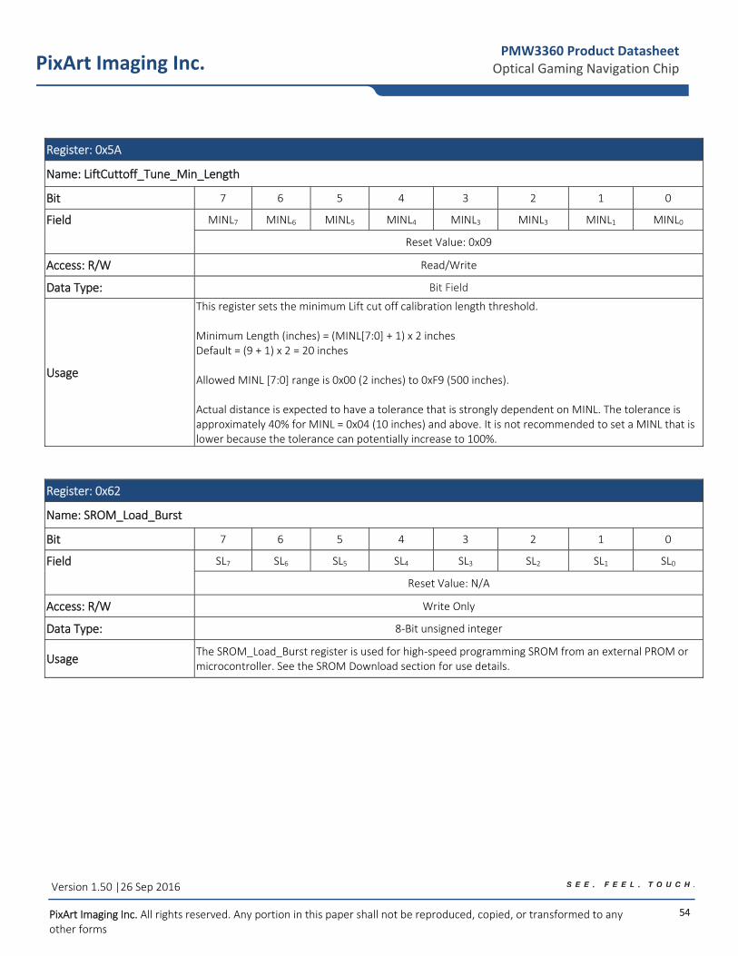
54
PixArt Imaging Inc. PMW3360 Product Datasheet
Optical Gaming Navigation Chip
Version 1.50 |26 Sep 2016
PixArt Imaging Inc. All rights reserved. Any portion in this paper shall not be reproduced, copied, or transformed to any other forms
Register: 0x5A
Name: LiftCuttoff_Tune_Min_Length
Bit 7 6 5 4 3 2 1 0
Field MINL7 MINL6 MINL5 MINL4 MINL3 MINL3 MINL1 MINL0
Reset Value: 0x09
Access: R/W Read/Write
Data Type: Bit Field
Usage
This register sets the minimum Lift cut off calibration length threshold. Minimum Length (inches) = (MINL[7:0] + 1) x 2 inches Default = (9 + 1) x 2 = 20 inches Allowed MINL [7:0] range is 0x00 (2 inches) to 0xF9 (500 inches). Actual distance is expected to have a tolerance that is strongly dependent on MINL. The tolerance is approximately 40% for MINL = 0x04 (10 inches) and above. It is not recommended to set a MINL that is lower because the tolerance can potentially increase to 100%.
Register: 0x62
Name: SROM_Load_Burst
Bit 7 6 5 4 3 2 1 0
Field SL7 SL6 SL5 SL4 SL3 SL2 SL1 SL0
Reset Value: N/A
Access: R/W Write Only
Data Type: 8‐Bit unsigned integer
Usage The SROM_Load_Burst register is used for high‐speed programming SROM from an external PROM or microcontroller. See the SROM Download section for use details.
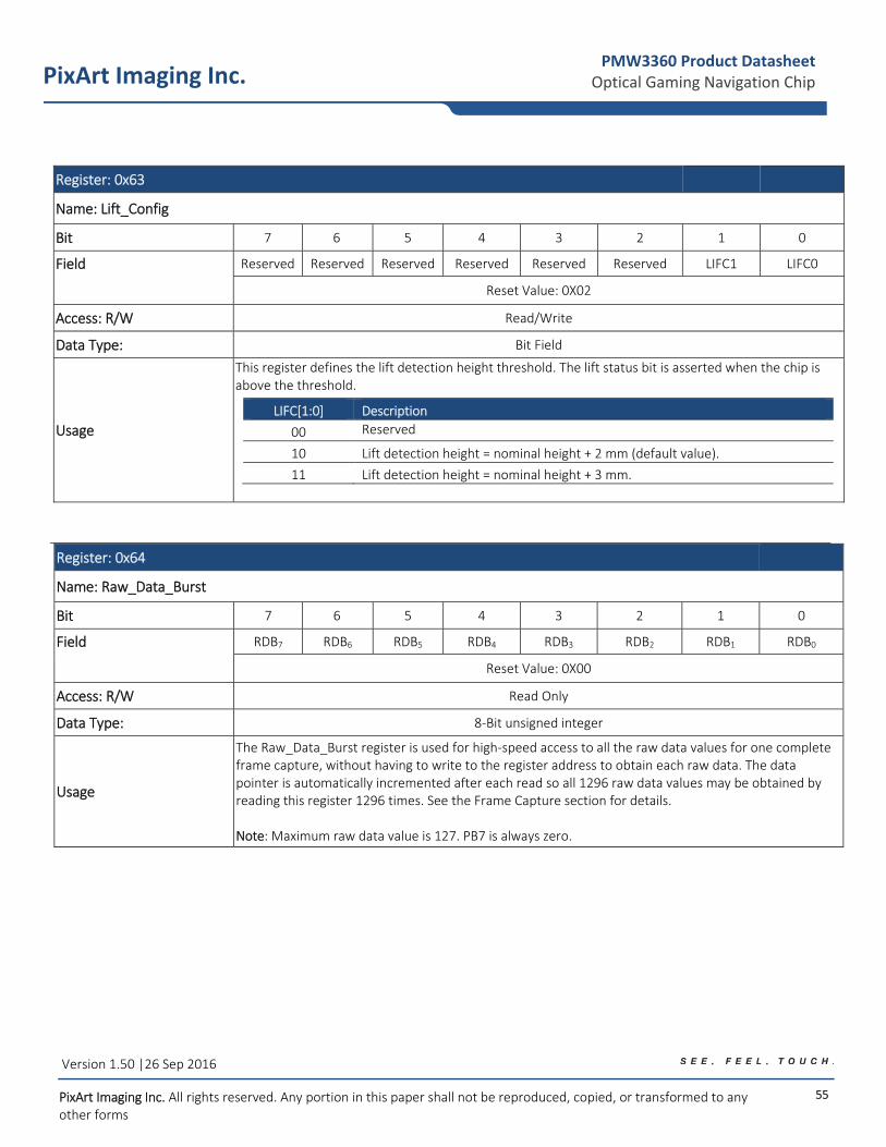
55
PixArt Imaging Inc. PMW3360 Product Datasheet
Optical Gaming Navigation Chip
Version 1.50 |26 Sep 2016
PixArt Imaging Inc. All rights reserved. Any portion in this paper shall not be reproduced, copied, or transformed to any other forms
Register: 0x63
Name: Lift_Config
Bit 7 6 5 4 3 2 1 0
Field Reserved Reserved Reserved Reserved Reserved Reserved LIFC1 LIFC0
Reset Value: 0X02
Access: R/W Read/Write
Data Type: Bit Field
Usage
This register defines the lift detection height threshold. The lift status bit is asserted when the chip is above the threshold.
LIFC[1:0] Description
00 Reserved
10 Lift detection height = nominal height + 2 mm (default value).
11 Lift detection height = nominal height + 3 mm.
Register: 0x64
Name: Raw_Data_Burst
Bit 7 6 5 4 3 2 1 0
Field RDB7 RDB6 RDB5 RDB4 RDB3 RDB2 RDB1 RDB0
Reset Value: 0X00
Access: R/W Read Only
Data Type: 8‐Bit unsigned integer
Usage
The Raw_Data_Burst register is used for high‐speed access to all the raw data values for one complete frame capture, without having to write to the register address to obtain each raw data. The data pointer is automatically incremented after each read so all 1296 raw data values may be obtained by reading this register 1296 times. See the Frame Capture section for details. Note: Maximum raw data value is 127. PB7 is always zero.
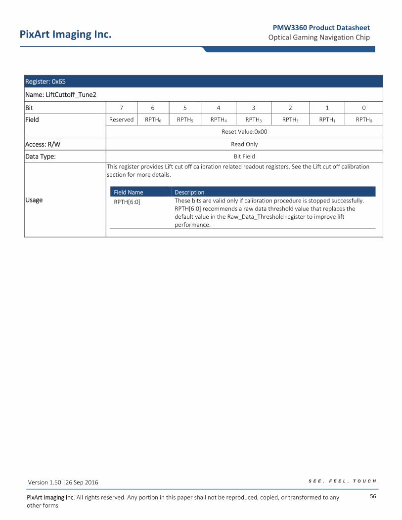
56
PixArt Imaging Inc. PMW3360 Product Datasheet
Optical Gaming Navigation Chip
Version 1.50 |26 Sep 2016
PixArt Imaging Inc. All rights reserved. Any portion in this paper shall not be reproduced, copied, or transformed to any other forms
Register: 0x65
Name: LiftCuttoff_Tune2
Bit 7 6 5 4 3 2 1 0
Field Reserved RPTH6 RPTH5 RPTH4 RPTH3 RPTH3 RPTH1 RPTH0
Reset Value:0x00
Access: R/W Read Only
Data Type: Bit Field
Usage
This register provides Lift cut off calibration related readout registers. See the Lift cut off calibration section for more details.
Field Name Description
RPTH[6:0] These bits are valid only if calibration procedure is stopped successfully. RPTH[6:0] recommends a raw data threshold value that replaces the default value in the Raw_Data_Threshold register to improve lift performance.

57
PixArt Imaging Inc. PMW3360 Product Datasheet
Optical Gaming Navigation Chip
Version 1.50 |26 Sep 2016
PixArt Imaging Inc. All rights reserved. Any portion in this paper shall not be reproduced, copied, or transformed to any other forms
12.0 Document Revision History
Revision Number Date Description
1.00 19 Aug 2014 - Initial creation
1.10 26 Nov 2015 - pg8 update Fig6 Lens Outline Drawing
- pg10 update Fig8 Recommended Base Plate Opening
- pg28 add item #3 Delay for 30mis
1.20 25 Feb 2016 - pg23 add point #8 Write 0x00 to Config2 register for wired mouse or 0x20 for wireless mouse design
1.30 6 Apr 2016 - pg47 add Register 0x29 Pix_Grab information
1.40 3 Aug 2016 - pg55 modify Register 0x63 Lift_Config register information. Removed setting 0x00
1.50 26 Sep 2016 - Update document. Change “sensor” to “chip”& “pixel” to “raw data”
- Change PixArt RoH Logo
- Change Image Array to Picture Element Array