
PM[DilEhAUTOilMAH - AirBorn · This manual assumes that you are familiar with some DOS operations...
272
PM[DilEhAU PtrOTEL TECHNOLOGY
Transcript of PM[DilEhAUTOilMAH - AirBorn · This manual assumes that you are familiar with some DOS operations...

PM[DilEhAUTOilMAH
PtrOTEL TECHNOLOGY


PnorEL-AuTorRAxReference Manual
A Printed Circuit Board Design Program

sorrware copyright @ re88 prorel;3#:[ pu LrdOriginal Reference Manual Copyright @ 1988 Protel Technology Pty Ltd
PROTEL TECHNOLOGY PTY LTDTechnopark, Dowsings Point,
Hobart, Tasmania, Australia.
Tel. National (002) 73 0100
Tel. International + 6l 0273 0100
Telex AA58260 CRTEC
Facsimile National (002) 73 l87l
Facsimile International + 61 02 73 1871
PROTEL TECHNOLOGY II.{C.
50 Airport Parkwa!,
San Jose, CA. 95110.
Tel. 408 43 7777I
Telex 510 100 7634
Facsimile 408 43 77777
Members of the CRITEC CORPORATION
Epson FX-80@ is a registered trademark of Espon America, Inc.
IBM6 is a registered trademark of International Business Machines Corporation.
PC-DOS6 is a registered trademark of International Business MachinesCorporation.
Microsoft6 is a registered trademark of Microsoft Corporation.
MS-DOS@ is a registered trademark of Microsoft Corporation.
FIP6 is a registered trademark of Hewlett-Packard Co{p.
Herculesrr,a is a trademark of Hercules Computer Technology.

lntroductionCongratulations on your purchase of PnorEL-AworRAx. As you
will soon see it contains exciting features which take the hardship
out of the process of designing printed circuit boards.
The program has been written by PROTEL TECHNOLOGY PTY
LTD an Ausgalian company which specialises in ttre development
of softwa.re products for the design of printed circuit boards.
pnornuAworRax is the latest addition to the PROTEL family of
CAD software and incorporates a host of ideas which have come
from many thousands of international users of the PROTEL'
ScnnuATIC and Pnornt-PCB progams.
pnornuScrtEMATIC is a program which will help you produce
excellent quality schematic d.rawings whether they be for design
verification or for a permanent record of a circuit. When used in
conjunction with PnornL-AworRAx you have a very powerful end-
to-end design system . PnornL-SCHEMATIc allows you to produce a
netlist (summary of electrical connections) of the schematic. With
is netlist capture feature, plus the automatic placement of
components and autorouting of tracks on the PCB , PROTEL-
AworRAX provides all the features you need to produce high
quality camera-ready artwork on either an ink plotter, photoplotter,
dot matrix or laser printer.
Pnornr-AworRAx now becomes PROTEL's high-end PCB design
program whereas PnortL-PCB caters for low-end users who just
wanr ro produce a quick layout of a PCB without using the
sophisticated features of P nornL'AworRAx -
Before reading further we ask you to read the Licence Agreement
which is in the front section of this manual. This request is made for
your benefit. Information about upgrades to the software and new
product information can only be sent to registered users. After
reading the licence details please fill in ttre regisradon card wi*t
your postal deuils and send it back to us.

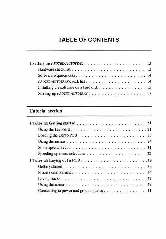
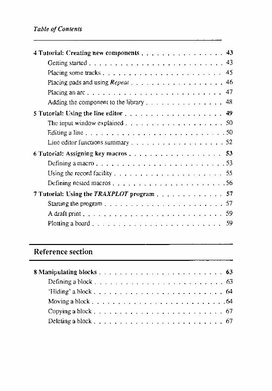
Table of Contents
4 T u t o r i a l : C r e a t i n g n e w c o m p o n e n t s , . , . , , , . . . . . , . . . 4 3
Ge t t i ngs ta r ted . . r . . . . . , . . . . . , . . . . . r . . r . 43
Plac ingsomeEacks. . . , , , r r . . . . i . , r t . . . . . 45
P lac ingpadsandus ing Repeat , , - . . r . . . . . . . . . . . . 46
P l a c i n g a n a r c . . . I r I r . | | | | . r . r | . , . r | . . . r 4 7
A d d i n g t h e c o m p o n e n t t o t h e l i b r a r y . . . . . . . . . . 4 8
5 T u t o r i a l : U s i n g t h e l i n e e d i t o r . . . . . . . . . . . 4 9
The inpu tw indowexp la ined . . . . , . . . . . . . . . . . . . . 50
E d i t i n g a l i n e . . . . 5 0
L i n e g d i t o r f u n c t i o n s s u m m a r y . . - . . . . . . . . . . . 5 2
6 T u t o r i a l : A s s i g n i n g k e y m a c r o s . . . . . . . . . ! . . 5 3
D g f i n i n g a m a c r o , . . , r . . . . . . . . . . . , . . . . . 5 3
Using the record facility . . . 55
Def in ingnest"edmacros. . . . . . . . r . . . r . . . . . . , . .56
TTutor ia l : Usingthe TRAXPLOTprogram . . . . . , . . . . . . 57
Srart ingtheprogram. - . . . . . . . . . . . . . . 57
A d r a f t p r i n t . . . . . . . . . r . . . . . . . . . r , . . , . r 5 9
P l o t t i n g a b o a r d . . . . . . . 5 9
Reference section
S M a n i p u l a t i n g b l o c k s . , . . . o . . . r . . . r . 6 3
Dgf in ingab lock , . , . r r . . r . . . . . r . . . . . , . . . . 63' H i d i n g ' a b l o c k .
. . &
M o v i n g a b l o c k . . . . . . r . r . . . r . . . . . . , . . &
Copy ingab lock . . , . . , . . . . , . . . , . . . . . 67
D g l e t i n g a b l o c k . . , . . , . . , . . . . , . . . . . 6 7

Table of Contents
Read ingab lock . . , , . r . t . r . . r . . r r . r . , , r r . 68
Sav ingpa r to fa layou t . . . . . . . . . . . . , . . . . . . . . 68
gViewingandChang ing thecur ren tSet t ings . . . . . . . . . . . . .69
Seningthecursormode. . . . . . . . . . . . . . . . . . r - . ,69
Sett ingaf loat ingorigin. r . . . . , . , . . . . . . , . . . . . .69
Thgcu lTgn t l yse lec ted laye r . . r . . . . . . . . , , r . . - . - , ' 70
ThecuTentpadt)n)e. . . . . . . . . . . . . . . . . r . . . . . 10
Padorientation. . . . . . . . r . . . . . . . . . . . . . . . . . 7l
Thedefaul t t rackwidth. . . . . . . - . . . . . . . . . . . . . .7L
Checkingthetextheight. . . . . . , . , . . . . . . . r . . - 72
Checkingthewidthofstr ingl ines. . . . . . . . . . . . . . . 72
Thedefaul tv ias izg. . . . . . r . . . . . . . . . . . . . . . . . '72
T h e d e f a u l t v i a h o l e s i z e . . . . . . , . , . . . . . . . . . . . 7 2
l0Dgtet ingi temsontheboard . . , , . , ! . . . . , . , , r . . . '73
De lg t inganarc . . . . . . . . . . . r . . . . . . . . . . . . . . ' 13
D g t e t i n g a c o m p o n e n t . . . . . , . . r . . . r r . , . r , . . r 7 4
Delgt ingafi l l . . . . . . . . . . . r . . . . . . r . . . . . . , '74
D g l e t i n g a h i g h l i g h t . . . . . r , r . ! , ! , , . . , r . r . 7 5
Dglet ingapad. . . . . r . . . . . . . . . . . . r . . . . , . . 75
Delet ingastr ing. . . . . . . . . . . . . . . . . . r . . . . . . 75
Delet ingatrack. . r . . . r , . . . . . , . . . . . . . r . . , 76
D e l e t i n g a v i a . . . . . r . . . . . . . r . . . . . . . . . . . 7 6
11 Chang ingpa r to f t hgPCB. . . . . . . . , , . . . . . . . . . . . 77
Chang ingacomponent . . . . . . . . . . . . . . . . . . . . . .77
Chang ingapad. . . . . . . . . r . . , . r . . . . . . . . . . ' 19
Changingatrack. . . . . r . . . , . . . r . . . ! . . . . . . 80
Changingastr ing. . , . , . . r r . , r . . . . . . r . r r . . .80
C h a n g i n g a v i a . . . . . . . . . . . . . . . . . . . . . . . . . 8 1

Table of Contents
1 2 M a n a g i n g f i l e s . . . , r . . , . . . r , , . . , , r , ! . . r r r . 8 3
Clearingfhememory. . . . . . . r . . . e . . , . . . . . . . 83
I s s u i n g D O s c o m m a n d s . , , . ! , , . , , , . , , , . ! , , , , 8 4
Check ing f i less to redonthed isk . . . . . . . . . . . . . . . .84
L o a d i n g a f i l e . . . , . r . . r r . . . , r . . . r , r , . . , 8 5
S p e c i f y i n g a p a t h n a m e f o r f i l e s . . . . . . . . . . . . . 8 6
L e a v i n g t h e P n o r m - A v r o r n A x p r o g r a m . ! , . , . ! . , , . , 8 7
Sav ingyou r f i l es . . . . . . . . . . . . , . . . r . . . . . . . 87
13Sg t t i ngg r i ds i zes . . . . . . . . r . . r . . . . . . . . . . . . . . 89
C h a n g i n g t h e ' s n a p ' g r i d . , . . . . . . . . . . . . . . . . . 8 9
Changingthevis ib lggr id. . . . . . . . . . . . . . . . . . . .90
14High l igh t ingnets . . , , . . . . . . . . . . . . . . . . . . . . . 91
H igh l i gh t i ngaconngc t i on . . . . . . . . . . , , . . . . . . . 9 l
Dupl icat ingnets. . . . r . . , . r , r r , . r r , . . . r r r . 92
H i g h l i g h t i n g a n g t . . . . . . . r . . . . . . . . . . - . . . . r 9 3
Creat inganet l i s t . , . . , r , r ! r , t r . . . . . . r , r r , . 93
l 5 G e t t i n g i n f o r m a t i o n a b o u t t h e b o a r d , . , , , . , , ! . , , , , 9 5
Determin ing theboard 'sd imens ions . . . . . . . . . . . . , .95
L i s t i n g t h e c o m p o n e n t s a l r e a d y p l a c e d . . , , . , , . . , , . , 9 6
Check ingh igh l i gh tedp ins . . . . . . . . . . , . . . . . , . . 99
Checkingthenamesof l ibrarycomponents. , , , , , , , , . , . 96
L is t inga l l thenets . . . . . . . . . . . . . . , . . . . . . , , . 97
Specifyingpowerand ground plane nets . . . . . . . . . . . . . 97
E s s e n t i a l i n f o r m a t i o n a b o u t t h e b o a r d . . . . . . , . 9 - l
1 6 U s i n g t h e J u m p o p t i o n . . . r . . . . . . . . . . . . . , , . . . . 9 9
Jump ing toacomponen t . . . . . . . . . . . . . . . . . . . - . 99
Jumpingtoalocat ion, . , . . , . . , . . . . . . . . . . , . 100
J u m p i n g t o a n e t . . . . . . . . . . . . . . . . . . . . . . . r . 1 0 0
J u m p i n g t o t h e o r i g i n . . . , . . . . r . . . . . . , . . . . . 1 0 1
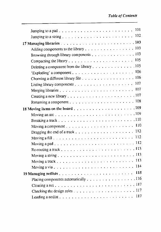
Table of Contents
Jumping toapad. . . ,
Jumpingtoastr ing . . . . . .
LTManagingl ibrar ies. . . . . .
Adding components to the library .
Browsing through library components
Compacting the library . . .
Dglgtingacomponentfrom the library - . . - . . - . . - . . .'Exploding' a component . . .,
Choosing a different library file . . .
Listinglibrarycomponents. . . . .
Merginglibraries. . . , . , . , . .
Creatinganew library . . . . . . .
Renaming acompongnt . . . . . .
1 8 M o v i n g i t g m s o n t h g b o a r d , . , . , . r , . . . . , , , . . r r .
Movinganarc . . . . . . . .
Break ingat rack . . , , r , , ! , ,
Mov ingacomponen t . . . .
Dragging the end of a Eack . .
Movingaf i l l r . . , . . . . . .
M o v i n g a p a d . . , . . . ,
R g - r o u t i n g a r a c k . . . . . , ,
Mov ingas t r ing . . . - . . . .
Mov ingat rack . . . . . . . .
M o v i n g a v i a . . . . . . . .
lgManag ingnet l i s ts . . . . . . . .
Placing components automatically. . | . . . . . . ' ' ' ' ' ' 1 1 6
Clear inganet . , tr7rr7rr7
a a a a a l a a " " "
101
r02103
103
103
105
105
106
106
r07
r07r07108
109
109
1 1 0
1 1 0
TL2
r12
r12
1 1 3
1 1 3
1 1 3
1 1 4
115
Checkingthedesignrules. . . . . , . . . . - . . - r . . . .
lnadinganetl ist . . . . . . .
Table of Contents
Hid ingnets . . . . r . . r , r . . , . . . . , r , . . , , . ! 118
Identi fy ingnets. . r . . . o . . . . . . . . . , . . r . . . . l l9
D e t g r m i n i n g t h e c o n n e c t i o n l e n g t h . , . , . , , , , . , . . 1 1 9L is t ingnetnames. . . . . . . . . . . . . . . . . . . . . . . . 119
O p t i m i z i n g n e t s . . . r , r ' r . . r r r . . r . r , . r r r . l l 9
Routingaboard. . . . . r . . . . . . . . r . . . . . . . , . . 120
S h o w i n g h i g h l i g h t s . . , . , . ! , , . , , r r . r . , r r . r l Z 0
Set t ingupthengt , f i les . . . . . . . . . . . . . . . . . . . . . . lZ0
2 0 R o u t i n g a b o a r d . . . . . , . . . . . r . . . . . . . . . . . . . l 2 l
I-ayersetup ' . ' . . . . . r . . . . - . . . . . . . . . , . . l2l
Se t t i ngup the rou te rpasses . . . . . . . . . . . . . , , . . 122
Separationsetup. . . . . . . r . . . . . . . . . . . . . . . .124
Set t ing theroutgrvar iab lgs . . , . . . . . . . , . . . . . . l2S
Rout ing theboard . . . . r . . . . , . . . . . . . . . . . . . . lZ5Routingasingleconnection . . . . . . . . . . . . . . . . . . . l?s
Routingaconnectionmanually . . . . . . . . . . . . . . . . . lZ9
Rout inganet . . . , . . . . . r . . i . . . . . . . . . . l2g
U s i n g t h e p a d t o p a d r o u t e r . . . . . . . . . . . , . . . . . l Z 9
2 l P l a c i n g i t g m s o n a b o a r d . . . , r . . . . . . . . . . ! . . , . . 1 3 1Plac inganarc . . . . . . . r . . . . . . . . . . . . . . . . l3 l
Placingacomponent. . . . . . . . . . . . . . . . . . . . . . 132
C r g a t i n g a n e x t e r n a l p l a n e . . . . . . . , , . . . . . . . r . , 1 3 3
Placingafil l . . . . . . . . . . . . . . . . . . r r . . . . . . 134Plac ingapad. . . r . , . . . . . . . . . . . . . . . . . . r 135
Placingastr ing. . . . . . . . . . . . . . . . . . . . . . . 135
Placingtracks. . . , . . . . . . . . . . . . . . . . . . . . r . 135
Placingavia. , . . . . . . . , . . . . . . . . . . . . . 136
2 2 R e p e a t i n g a c t i o n s . . . . . . . . . . . . . . . . . . . , . , . , 1 3 7

Table of Contents
23 Changing the setuP oPtions
Controlling componenl text
Choosing layer colors . . .
Selecting menu colors . . .
t t l l a r t t t t t " ' t l t l '
a a a a l a a a - " " " '
a a a a a . l a a t t t l t t l ' 1 "
24
25
Assigning functions to keYs . , .
Sett ingOpt iOnS. . . . . . . . . . r . . . . . . . . . r . . . .
Dgf in ingpadtypes , . . r , r ' , . . ! r . , . . . r . . r ,
Choosing the redraw qualitY
Sett ingstr ingdefaults. . , , . ,
Turning layers on and off
Using the un-delete command
Expandingand contract ingthedisplay . . . . . . . . . . . .
Redrawing the screen . .
Moving around the board
Expanding the display . .
Contracting the display . . ,
F i t t i n g t h e b o a r d o n t h e s c r e e l l , . . . . . . . . . . . . .
S p e c i f y i n g a z o o m f a c t o r . . , , . . , , . . ! r , . , , . . ! .
Selecting a zoom value .
139
r39
140
t4l
t4l
r46
148
150
150
r 5 1
153
155
155
155
156
156
156
156
157
S p e c i f y i n g a z o o m w i n d o w . . . . , . . . . . , ' . . . . . I 5 7
Utilities section
26Us ing theTRAXPI 'OT program. . . . . . . . . . . . . . .
StartingtheTRNQLOT program, , , . , . . . . , . . . . . .
TheF i l eme l l u . . . .
Displayinginformationabouttheboard. . . . . - . . - . . - .
Choosing the plot options . . ,
161
1 6 1
r62r&165
LffiThesetupopt lon. , , , , .
Table of Contents
Pr int ingorp lot t ingaPCB, , r , . , . , r . ! , r , . , r , , , I7A
ZTThePCB3CON and PLIB3CON programs. . . . . . . . . . . .l7lT h e P C B 3 C O N p r o g r a m . . , . . . , . . . . . . . . . . . . , 1 7 1Thg PUB3CONprogram. . . . . , . . . . . . . . . . . . . 172
Appendices
A Features of PnorEL-AurorRAX . . 17 5
Importantfi les. . . r . r . . . . , . . . . . . . . . . . . 175
H a r d w a r e a n d s o f t w a r e c h e c k l i s t . . . . . 1 7 8
Hardwarerequirgments. . . . . . . . . . , . . . r r , . . . . 178
Softwarerequirgments. . , . . . . , . . . . . . . . . . . . 180
P n o r c t - A w o r n u r c h e c k l i s t . . . . . . . . . . . . , . 1 8 0
Paramgters . . r | . r ! | r . , . . . . . r . , t . . , t . . 181
B R S - 2 3 2 C o n s i d g r a t i o n s . , . , . . . . . . . ! , . . r , . ! . r . 1 8 3
S e r i a l v e r s u s p a r a l l e l i n t g r f a c e s . . . , . . . , . . . , . , . . . 1 8 3
Cab lgconnect ions . . r r r r . . r , . . . . . , r r , . r , .184
B a u d r a t e r d a t a b i t s r e t c . . . - . . . . . . . . . . . . i . . . . . 1 8 5
W h a t t o d o i n c a s e o f p r o b l e m s . . . , , , , . , , , , . ! . , 1 8 6
C E r r o r m e s s a g e s . . . . . , r . . . . . . . . . . , . . . , . . . . 1 8 9
Non- fa ta l g r ro r s . . . . . . . r . r . . , . . . . ! . . . . . 189
F a t a l g l T o r s . . . , . . . . . , . . . . . . . 1 9 7
D A n o t e t o e d u c a t o r s . , . . . . . . . . . . 1 9 9
Index
Index . . . . . . . . . . . . . . . r , . . . . . . . . . . . . . . . ,2A3

1 sETTTNG uP PRITEL-AUTITRAr
Pnornt-Avrornur is a low-cost, yet powerful, software package forproducing printed circuit board (PCB) artwork. I[ is a fully-feanrredsystem which runs on the IBM-PCIXT/AT series and close compatibles.
This chapter details the hardware and software you will need to run theprogram and provides some advice on installing the software.
Hardware check listYou will need the following:
An IBM microcomputer or compatible
2 floppy disk drives or one floppy drive and one harddrive (a hard disk is recommended)
Graphics card (CGA, EGA, Hercules, VGA or VegaDeluxe)
Colour monitor
One parallel printer port
Microsoft mouse or compatible (recommended)
Draft printer
MS-DOS or PC-DOS (Version 2.0 or greater)
You will need access to:
A pen and ink plotter
A Gerber-compatible photoplotter
An Excellon format N/C drill
For the exact hardware requirements, you should check Appendix A atthe back of this manual.
13
Chapter I
The maximum size of a .PCB file which can be loaded by Pnornu
Aurornm in the standard 640K RAM is approximately l80K bytes.
Files bigger than this will not load and therefore require the use of
expanded memory systems (EMS).
If you decide to purchase extra memory, please note that you require an
Expanded Memory Board rather than an Extended Memory Board.
The board should conform to the widely used LIM standard. We have
used the 'Hyperam AT' board by Hypertech when designing the
program.
Software requirementsIn addition to the Pnorrt-Atnornax software you will need a copy of
either the MS-DOS or PC-DOS operating system. The version number
should & 2.0 or greater.
This manual assumes that you are familiar with some DOS operations
such as creating directories, changing directories, specifying path names,
formatting disks, deleting files and copying files.
The software will provide automatic backups of your files, but it is
strongly recommended that a regular backup of PCB files is made onto a
different disk.
Pnorct-AurorRAx check I istWhen you receive your Pnornr-Avtornil( package you should find the
following contents:
The P nortr-Avtornur manual.
Four diskettes, labelled Program Disk A, Program Disk B,
Library Disk and Plot Disk which contain the Pnorsu
Aurornur programs and ttreir associated files.
The external protection device, which plugs into one of
the parallel printer ports of your microcomputer and
allows the Pnorgt-Aurornur program to work. It alsoprevents unauthorised use of the software.
I4
S e ning up P norEL-AworRAX
The Software License Agreement Card, which you shouldfill out and return immediately. This is vital if you requirefurther support or information about future updates andrevisions.
Note that you can make unlimited backup copies of the disks, but themain program will only work if the external protection device is pluggedinto one of the parallel ports.
lnstalling the software on a hard diskYou should immediately make a backup copy of each disk and store theoriginals in a safe place.
If you are using the programs from a hard disk, make a subdirectorycalled \Protel and copy all the Pnornr-Awornetr files into thissubdirectory. Create another directory called \PCB to store your PCBfiles. It is strongly recommended that you store your files in a differentsubdirectory to the Pnorst-ArnornAx system files. This makes it easierfor you to create backups of your work.
The following instructions provide one means of setting up your harddisk.
Move to the top directory on disk C:
Type: MD Protel and press (<ENTER>>
Type: MD PCB and press (ENIER>
Type: CD Protel and press <<ENTER>>
The prompt should now indicate that you are in the \Protelsubdirectory (e.9. C:Wotel>)
Put Program Disk A disk in drive A:
Type: COPY A:*.* and press <ENTER>>
Put Program Disk B disk in drive A:
Type: COPY A:*.* and press <ENTER>
Put the Library Disk in drive A:
Type: COPY A:*.4 and press <<ENTER>>
I5

Chapter I
Now put the Plot Disk in drive A:
Type: COPY A:*.* and press <ENTER>>
All the programs and files should now be installed on your hard disk.
If you want the computer t0 place
automatically, then you will need toAI-IIODGC.BAT file.
The command you need to use is:
CD \PCB
If you do not know how to change the file then seek help - it is not agood idea to change this file if you are not confident about the DOS
environment.
The next step is to select a graphics driver program which suits the
graphics card you have in your microcomputer.
When the Pn orm-AurorR*( program is loaded it looks for a file called
GRAPH.DRV. This file contains the information required to drive the
graphics display. If no GRAPH.DRV file is found, the software assumes
that you are using a CGA card. If you are using an EGA, VGA, Hercules
or Vega Deluxe card then you must create the appropriate GRAPH.DRV
file.
The instruction you should type at the DOS prompt is shown in the table
below:
you in the PCB subdirectoryput an extra command in the
Instruction
EGA
VGA
VEGA
HERCULES
Card type
EGA
VGA
Vega Deluxe
Hercules
If you later wish !o return to using a CGA card then type:
CGA then press <ENTER>
and the GRAPH.DRV file will be deleted.
Note that further graphics drivers may be made available in the future.
I6

S e ttin g up P nor E L-Awor RAx
Starting up Pnorct-Auror+AxIf you are using a floppy drive system, make sure that Program Disk is in
drive A: and Program Disk B is in drive B:. You should also set the DOS
PATH variable to point to drive B:. This is best done in the
AUTOEXEC.BAT file.
If you are using a hard drive system, you can run the programs from any
directory, but you may want to move into the directory in which you
want to store your PCB files just to be on the safe side.
If it is the first time you have run the program, select the appropriate
graphics driver as described on the previous page.
You are now ready to run the pro$am. Simply type:
TRAXEDIT and press <ENTER>
and the program will start.
If you are using a floppy drive system you can now take out Program
Disk A and replace it with the Library Disk.
You should now attempt some of ttre tutorials which will help you
become familiar with the features of PqoTEL-AUToTRN(.
I 7

Chapter I
I8
TI.]TORIAL SECTION


2 TUTORIAL: GETTING STARTED
This tutorial allows you to gain an overview of the features of Pnornt-Aurornur. It is suggested that you complete the tutorial beforeatfempting to create your own design even if you are familiar withprevious versions of ttre program. There are many new features whichyou need to master.
In this nrtorial you will learn the following skills:
using the keyboard;
identifying keys and using key combinations;
starting the Pn orruAworRil( program;
loading the DEMO file;
using the dropdown menus;
quitting from P norrt-Atnornex:
expanding and contracting the display;
using the crnsor keys and the mouse;
using the cursor keys with the <SHIFTT kty;
getting information about the board;
locating components, tracks, vias and pads;
changing setup options.
Using the keyboardThroughout this manual a number of conventions have been used to helpyou decide what to type. One convention is ttrat when a particular key isreferred to, it will be enclosed in chevrons. Thus if you are asked to typethe key labelled A it will be enclosed in chevrons thus, (<A>>. If you areasked to hold down the key marked SHIFT it will be referred to as<SHIFT>>, and so on.
2t

Chapter 2
The main section of the keyboard comprises a set of letter keys andnumber keys as well as some special keys. The one you need to becomefamiliar with immediately is the key labelled <ENTER>> or sometimes(<RETIJRN>) or sometimes simply an arrow. This key is often used tosignal that you have finished entering informalion.
Some keys are used in conjunction with one other key. These are the(<CTRL>>, <SHIFT>> and <<ALT>> keys. Often you will be asked to typesomething like <CTRL> <A>. This me€rns hold the <CTRL> key downwith one finger and press the <A> key with another. Another importantkey is <BACKSPACE> which deletes the character to the left of thecursor.
Keyboards vary considerably in their layout, but most have a set offunction keys which are labelled FI, F2, etc. Sometimes these are onthe left hand side of the keyboard and sometimes they form a line alongthe top. The use of function keys is optional with Pnorrt-Atnornax butthey can speed up operation considerably.
On the right hand side of the keyboard there is a numeric keypad. Somekeyboards also have a set of cursor keys (the keys with arrows on them)and some special keys between the main part of the keyboard and thenumeric keypad. The arrow keys will be referred to as (<LEFT>),
<RIGI{[>>, <<IJP>> and <DOWN>,. Other keys which will be used often arethose marked <HOME>>, (<ENID>>, <PGUP> and <<PGDN>>. The <DEL>key is used to delete the character which is currently highlighted.
If you have an 'AT'-sryle keyboard with the extra set of cursor keysbetween the main keyboard and the numeric keypad, then it is possiblethat the <<SF[IFT>> key will not work in conjunction with these cursorkeys.
If you are using a mouse then the left button will be refened to as<LEFT MOUSE> and is similar in operation to the <ENTER> key. Theright button will be referred to as <RIGHT MOUSE> and is similar inoperation !o the <<ESC> key. This usually takes you back one step orcancels an operation.
) )
T utorial: G etting S tarted
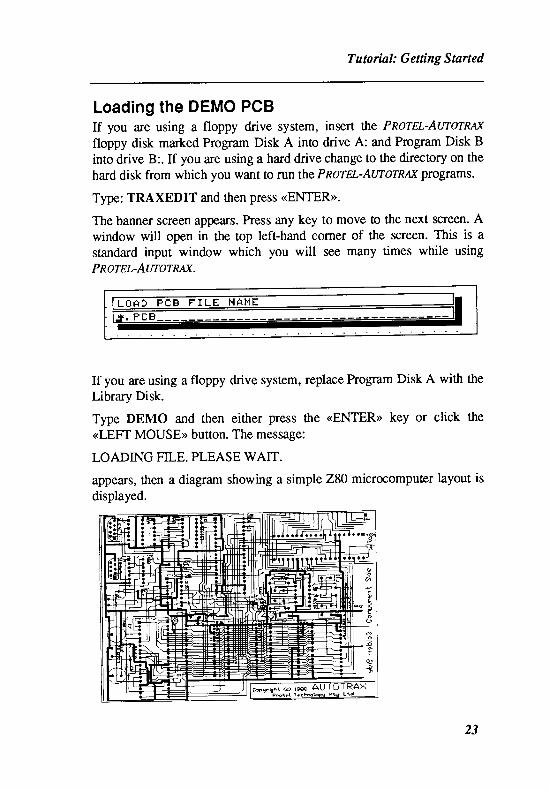
Loading the DEMO PCBIf you ile using a floppy drive system, insert the PnorsL-Atnornexfloppy disk marked Program Disk A into drive A: and Program Disk Binto drive B:. If you are using a hard drive change to the directory on thehard disk from which you want to run the Pn orEL-AworRN( programs.
Type: TRAXEDIT and ttren press (ENTER>).
The banner screen appears. Press any key to move to the next screen. Awindow will open in the top left-hand corner of the screen. This is astandard input window which you will see many times while usingPnorEt-AworRdlL
If you are using a floppy drive system, replace Program Disk A with theLibrary Disk.
Type DEMO and then either press the (<ENTER>) key or click the<LEFT MOUSE>> button. The message:
LOADING F[LE. PLEASE WAIT.
appears, then a diagram showing a simple 280 microcomputer layout isdisplayed.
f f iorRAx- -P'o.tct 163lrn5tcE9 ft/4' L{d
23
Chapter 2
Notice the status line at the bottom of the screen which gives importantinformation about the board and the position of the cursor. If you movethe mouse or press the cursor keys a few times the numbers whichindicarc lhe position of the cursor change.
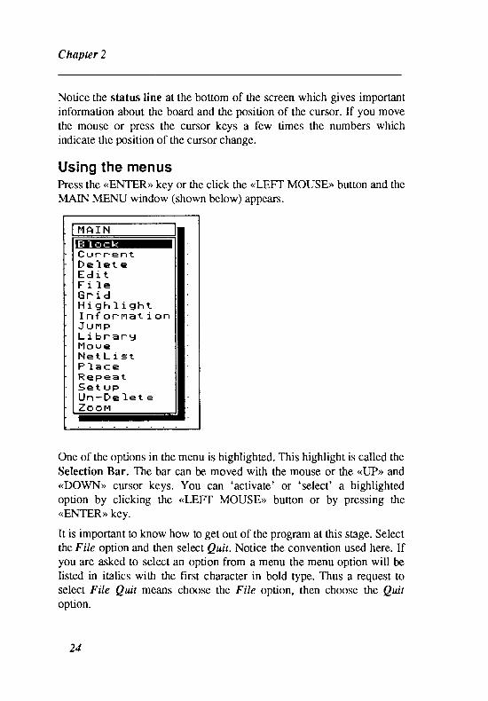
Using the menusPress the <ENTER> key or the click the <<LEFT MOUSE> button and theMAIN MENU window (shown below) appears.
1'IA I N
C u r r e n tD e l e t eE d i tF i l eG r i dH i s h l i e h tI n f o r m a t i o nJ u n pL i b r a r t ll " l oueN e t L i s tP l a c eR e p e a tS e t u pU n - D e l e t eZ o o F l
One of the options in the menu is highlighted. This highlight is called theSelection Bar. The bar can be moved with the mouse or the (<lJP>) and<DOWN> cursor keys. You can 'activate' or 'select' a highlightedoption by clicking the <LEFT MOUSE> button or by pressing the<ENTER>> key.
It is important to know how to get out of the program at this stage. Selectthe File option and ttren select Quit. Notice the convention used here. Ifyou are asked to select an option from a menu the menu option will belisted in italics with the first character in bold type. Thus a request toselect File Quit means choose the File option, then choose the Quitoption.
24

Tutorial: Getting Started
C l e a rD o sF i
. } 'es
L o a dP a t hIEilHTT5 a u e
A window opens which asks you to confirm that you want to qutt to
DOS.
Y e s
Choose the y es option if you do want to quit. Choose No to contmue
with this tulorial.
The demo circuit is too small to work with easily, so it needs to be
expanded. Choose zoom from the MAIN MENU. Remember to make
sure that it is highlighred, then click the <LEFT MOUSE> button or
press the <<ENTER> key to select the option.
The following window appears:
Z O O H
P a nE x p e n dC o n t l * e c tA l rK e g b o e r d5 e l e c tl J i ndoh ,
25
Chapter 2
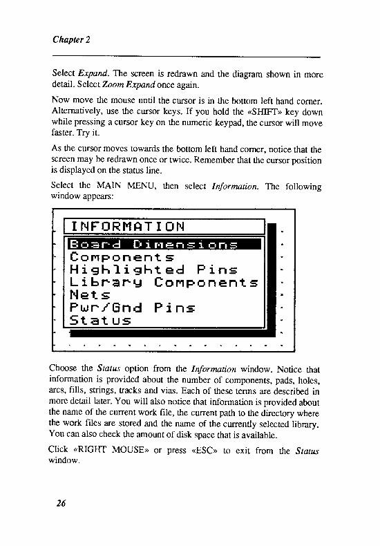
Select Expand. The screen is redrawn and the dia$am shown in moredetail. Select Zoom Expand once again.
Now move the mouse until the cursor is in the bottom left hand corner.Alternatively, use the cursor keys. If you hold the <SHIFT>> key downwhile pressing a cursor key on the numeric keypad, the cursor will movefaster. Try it.
As the cursor moves lowards the bottom left hand corner, notice that thescreen may be redrawn once or twice. Remember that the cursor positionis displayed on the st"atus line.
Select the MAIN MENU, then select Information. The followingwindow appears:
I TqFORI ' IAT I OTq
C o m F o n e n t gH i s h l i s h t e d P i r . r sL i b n e r l l t r o r q t r $ n e n t sI t let sP u r f E n d P i n s5 t a t u s
Choose the Status option from ttre Information window. Notice thatinformation is provided about the number of components, pads, holes,arcs, fills, strings, tracks and vias. Each of these terms are described inmore detail later. You will also notice that information is provided aboutthe name of the current work file, the current path to the directory wherethe work files are stored and the name of the currently selected library.You can also check the amount of disk space that is available.
Click <RIGHT MOUSE> or press <ESC> to exit from the Stattuwindow.
26
T utorial: G etting S tarted
5 T A T U 5
F r e e E n q s J ' l e n 4 o r uA r c sC o m P o n e n t sF i 1 l sH o l e sP a d s5 t r i n g sT n a c k sU i a sU o n k F i l e N a m eL i b n e F HC u r r e n t P a t hD i s k 5 i z eD i s k F n e e
6Et 53 6B42242251 5 3 5BD E 1 ' I O . P C BP C B S T D . L I BC : \ P C B2 1 3 4 9 4 4 6 B H t e sI 9 6 3 9 3 6 9 B s t e s
B g t e sB u t e s
Now try each of the other options in the Information window to
determine the board's dimensions, the components on the board, the
unconnected pins and so on. Press <ESC> or click the (RIGHT
MOUSE> button to exit from this menu-
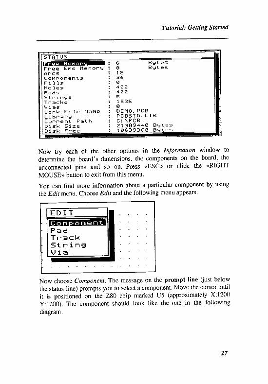
you can find more information about a particular component by using
the Edir menu. Choose Edit and the following menu appears.
E D I T
P a dT r e c kS t r i n gU i a
Now choose Component. The message on the prompt line (ust below
the status line) prompts you to select a component. Move the cursor until
it is positioned on the 280 chip marked U5 (approximately X:1200y:1200). The component should look like the one in the following
diagram.
27
Chapter 2
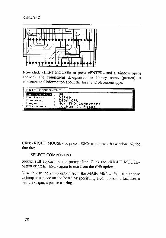
Now click <LEFT MOUSE> or press <ENTER>> and a window opensshowing the component designator, the library name (pattern), acomment and information about the layer and placement type.
E D I T C O I { P O N E I {
F a t t e r nf , o n q m e n tL a H e rP ] a c e r { e n t
U 5D I P 4 BZ 8 g f l C P UI t f o t 51 ' lD Con ' r ponen tL o c k e d I n P l a c e
Click <RIGHT MOUSE>> or press <ESC> to remove the window. Noticethat the:
SELECT COMPONENT
prompt still appears on the prompt line. Click the <RIGHT MOUSE>button or press <ESC> again to exit from the Edir opdon.
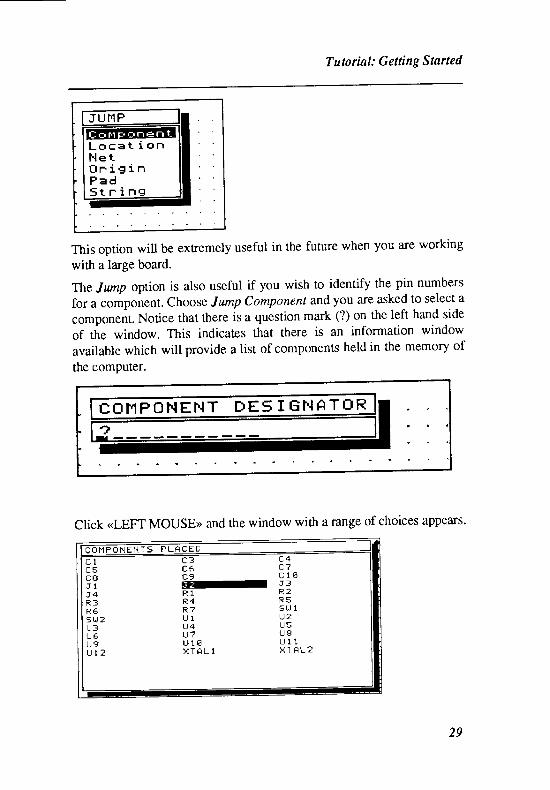
Now choose the Jump option from the MAIN MENIJ. You can chooseto jump to a place on the board by specifying a component, a location, anet, the origin, a pad or a string.
28
Tutorial: Getting Started
J U H P
L o c a t i o nH e tO n i s i nP a d5 t r i n
This option will be extremely useful in the future when you are working
with a large board.
The Jump option is also useful if you wish to identify the pin numbers
for a component. Choos e Jump Component and you are asked to select a
component. Notice that there is a question mark (?) on the left hand side
of the window. This indicates that there is an information window
available which will provide a list of components held in the memory of
the computer.
click <LEFT MOUSE> and the window with a range of choices appears.
C O T " I P O N E N T 5P L f , C E D
c lC 5c 8J 1J 4R 3R 55 U 2U 3U 6U 9u l 2
c 3 c 4c 6 c ?c 9 c l 8i l J 3n r R 2R 4 R 5R ? 5 U tu l u zu 4 u 5U ? U SU l E U l TX T P L 1 X T A L z
a a
t l a
I t a
29
Chapter 2
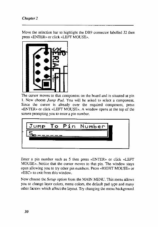
Move the selection bar to highlight the DB9 connector labelle d JZ thenpress (ENTER>> or click <LEFT MOUSE>>.
The cursor moves to that component on the board and is situated at pinl. Now choose Jump Pad. You will be asked to select a component.Since the cursor is already over the required component, press<ENTER>> or click (<LEFT MOUSE>>. A window opens at the top of thescreen prompting you to enter a pin number.
Enter a pin number such as 5 then press <<ENTER> or click <LEFTMOUSE>>. Notice that the cursor moves to that pin. The window staysopen allowing you to try other pin numbers. Press <RIGHT MOUSE>> or<<ESC> to exit from this window.
Now choose the Serup opaon from the MAIN MENU. This menu allowsyou to change layer colors, menu colors, the default pad type and manyottrer factors which affect the layout. Try changing ttre menu background
T i*
I
30

Tutorial: G etting Started
color by choosing Menu Color ttren clicking <LEFT MOUSE> or
pressing <ENTER>> and observing the changes in color. Press <<ESC>' or
Itirt <RIGF{T MOUSE>> when you have finished selecting colors.
S E T U PTEJIruL a ! J e r C o l o r sH e n u C o l o r sK e g sO p t i o n sP a d sR e d n a h J5 t r i n g gToss 1e La UEr -=
t t a
a a l
By now you should be familiar with the menu structure of Pnorsr'
Aurornur and some of the features of board layout. No attempt has been
made to place components or Eacks or to change layers. This will be
done in subsequent chaPters.
Some special keYsThere are some other keys which have a special function in the Pnornu
AUrOfnm program. These are explained below:
(<END>> Redraws or 'refreshes' the screen'
<HOME>> Centers the screen about the current cursor
position.
<<pGUp>> This key has the same effect as choosing Zoom
Expand.
(<pGDN>) This key has the same effect as choosing Zoom
Contract.
it also has <PRTSC> on the same key. It is used
to swap between the top layer and the bottom
layer. The effect can be observed on the status
line.
3I
Chapter 2
This key is also on the keypad. It is used to cyclethrough all the currently selected layers.
(<+>) This key is also on the keypad. It is used !o cycle
ffi:i,illffiffilJ"::jffi: ravers in the
Speeding up menu select ionsBefore finishing this tutorial you should be aware of a feature ofPnorst-Avtornest which helps speed up menu selections once youbecome familiar with the menu structure.
Each menu option can be chosen by simply pressing the first key of theoption to be selected. Thus to choose Jump Pad you only need to type Jthen P.
You should now quit from the program by choosing File from the MAINMENU, then choosing Quir (or by pressing F ttren Q) as described nearthe beginning of this tutorial.
32
3 TUToRIAL: LAYTNG our A PcB
In this tutorial the most important aspects of placing components, using
the libr?r!, taying tracks and using the powerful router will be covered.
The tutorial will lead you through the set of steps necessary to begin
designing an RS-232 splitter board. As there is insufficient space in the
manual to describe laying out the whole board, you will simply place a
DB25 connector and the first of the 16 pin chips as well as some by-pass
capacitors and a resistor.
In this tutorial you will learn the following skills:
clearing the work space;
choosing a component from the library;
placing a component;
rotating a componenq
assigning component designators and comments;
identifying pins on components;
placing tracks manuallY;
swirching layers;
saving a board;
using the pad to pad router;
creating a netlist;
using the automatic router.
Getting startedThe aim of this tutorial is to lay out the section of an RS-232 splitter
board shown below.
33

Chapter 3
There is one DB25 connector, one DIP16 chip, three capacitors and oneresistor on the board. Your first task is to place these.
You must first make sure that the board is clear. Either restart thePnornt-Atnornut pro$am or choogo, File Clear Yes. If you start theprogram again then press <<ESC> or click the <RIGHT MOUSE>> buttonin response to the prompt 'LOAD PCB FILE NAME'.
Placing componentsNow press <PGUP>> lhree times and choose Place Component. An inputwindow wittr ttre heading 'NAME IN LIBRARY' opens asking for thename of a pre-defined component. Notice that there is a question markon the input line. Press <ENTER>> or click the <<LEFT MOUSE> buttonand a list of the components in the library is displayed.
If you know ttre name of the component ttren you could have simplytyped it when the input window opened. In this case you would haveentered the name DB25 and pressed <ENIER> or clicked <LEFTMOUSE>).
For the purposes of this tutorial, however, select the component from thelibrary list as displayed below.
34
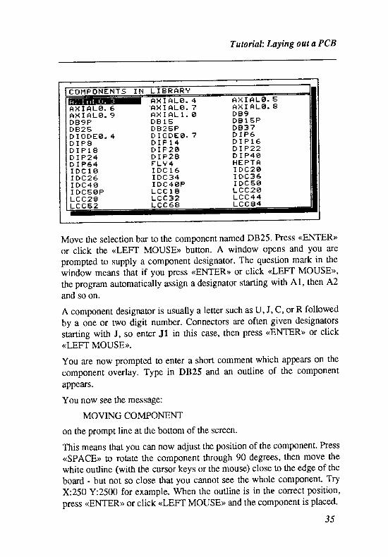
Tutorial: Laying out a PCB
C O1 ' IPONE NT 5 I N L I B R A R Y
f f X I A L E . 6A H I A L B . 9D B 9 PD B 2 5D I O D E g . 4D I P 8D I P l 8D I P 2 4D I P 6 4I D C 1 gI D C 2 6I D C 4 BI D C S 6 PL C C 2 8L C C 5 z
A X I A L g . 4. A X I A L B . ?
A H I A L l , 6D B 1 5D B 2 5 PD I O D E B , TD I P T 4D I F 2 BD I P z BF L V 4I D C 1 6I D C 3 4I D E 4 g PL C C 1 8L C C 3 2L C C 6 8
A X I A L B . 5R H I A L B . 8D B 9D B 1 5 PD B 3 ?D I P 6D I P l 6D T P 2 2D I P 4 BH E P T AI D C z BI D C 3 6I D C S SL C C 2 BL C C 4 4L C C 8 4
Move the selection bar to the component named DB25. Press <ENTER>>
or click the <LEFT MOUSE> button. A window opens and you are
prompted to supply a component designator. The question mark in the
window means that if you press <<ENTER>> or click <<LEFT MOUSE>>,
the program automatically assign a designator starting with A1, then A2
and so on.
A component designator is usually a letter such as IJ, J, C, or R followed
by a one or two digit number. Connectors are often given designators
starting with J, so enter Jl in this case, then press <<ENIER>> or click
<<LEFT MOUSE>>.
You are now prompted to enter a short comment which appears on the
component overlay. Type in DB25 and an outline of the component
appears.
You now see the message:
MOVING COMPONENT
on the prompt line at the bottom of the screen.
This means that you can now adjust the position of the component. Press
<SPACE> to rotate the component through 90 degrees, then move the
white outline (with the cursor keys or the mouse) close to the edge of the
board - but not so close ttrat you cannot see the whole component. Try
X:250 Y:2500 for example. When the outline is in the correct position,
press <ENTER>> or click <LEFT MOUSE> and the component is placed.
35
Chapter 3
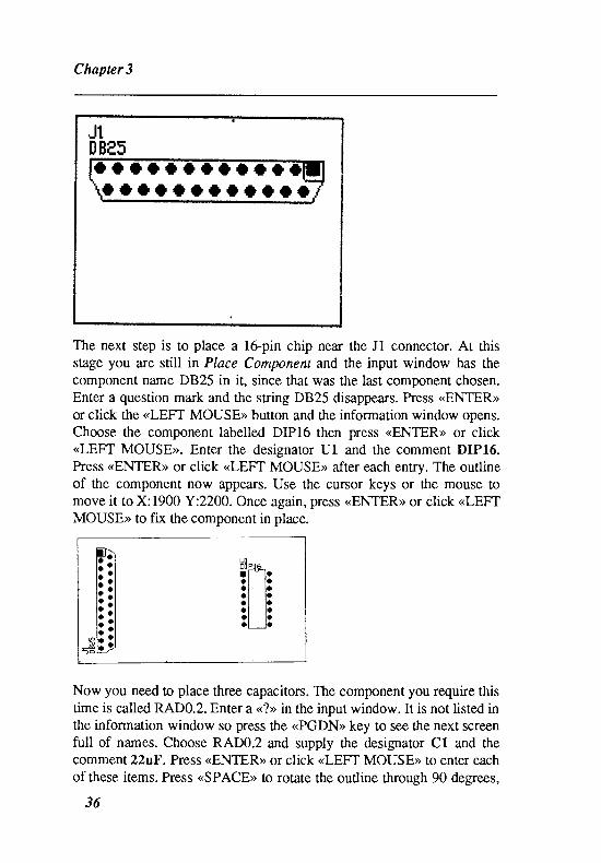
JT0Be5r r r l l r r * r T .l r f r r t t r t + t r
The next step is to place a l6-pin chip near the Jl connector. At thisstage you are still in Place Component and the input window has thecomponent name DB25 in it, since that was the last component chosen.Enter a question rnark and the string DB25 disappears. Press <<ENTER>or click the <<LEFT MOUSE>> button and the information window opens.Choose the component labelled DIP16 then press <ENTER> or click<LEFT MOUSE>>. Enter the designator Ul and the comment DIP16.Press <ENTER>> or click <LEFT MOUSE> after each entry. The outlineof the component now appears. Use the cursor keys or the mouse tomove it to X:1900 Y:22A0. Once again, press <ENTER>> or click <LEFTMOUSE>> to fix the component in place.
Now you need to place three capacitors. The component you require thistime is called RAD0.2. Enter a <<?>> in the input window. It is not listed inthe information window so press the <PGDN> key to see the next screenfull of names. Choose RADO.2 and supply the designator Cl and thecomment 22uF. Press <ENIER>> or click <LEFT MOUSE>> to enter eachof these items. Press <SPACE>) to rotate the outline $rrough 90 degrees,
36
UIDItooooooo
aooooooo
Tutorial: Laying out a PCB
then move it to X:'1350 Y:2250. Press <ENTER>> or click <LEFTMOUSE>> to place it.
The input window is still showing the name RAD0.2 so simply press<<ENTER>> or click <LEFT MOUSE>> to choose that name for the secondcapacitor. The designator automatically becomes C2 and the comment isstill 22uF. Rotate the second capacitor and place it on the other side ofthe DIP16 chip at X:2800 Y:2250. Now choose RAD0.2 a third time.Rotate it and move it to X:1350 Y:1150. Click <LEFT MOUSE> orpress (<ENTER>> to fix it in position.
Now move to a point just above C3 (say, X:1250 Y:1550) and choosethe component labelled AXIAL0.3. Assign the designator Rl and thecomment 3.3K. Press <ESC>) or click <RIGHT MOUSE> to exit fromthe Place Component option.
The display might be a bit messy by now so press the (<END>> key toredraw lhe screen.
Laying tracksNow you are almost ready to start laying Eacks. Before you cil, youneed to know the pin numbers of the components. In the previoustutorial you learned how to identify pin numbers using Jump Pad. Usethis option to find pin 1 on Jl, Ul, Rl and Cl. From this informationyou can work out most of the others. It might also be necessary to locateptn 25 on Jl and pin 16 on Ul.
The following table provides a list of the pins which must be connected.
Ul- l to C l -2
Ul -16 to C3- l
U1 - l I t o J l - 3
Ul -9 to Jl -4
U1-4 toQ.-2
Il-20 to Rl - l
U1-3 to C l - l
Ul -12 to I l-2
Ul -10 to J l -5
Ul -5 to C2-l
Ul-z to C3-Z to Rl-2
37
Chapter 3
The first entry in the table indicates that you must connect pin I on the
component Ul to pin 2 on the component Cl. The entry under it shows
that you must connect pin 16 on the component Ul to pin I on the
component C3.
This information becomes important later as it is the basis of the concept
of a Netlist. A netlist is a list of all connections on ttre board and is used
to make connections automatically with the Ne tlist Route option. Each
group of connections in a netlist (e.g.Ul-l to Cl-z) is called a Net.
Just in case anything goes wrong, save the board. To do this choose File
Save, supply a filename, then press <<ENTER>). Choose Yes to confirm
the fact that you want to save the PCB file.
Tryconnect ingthef i rs tcoup1eofpadsmanual ly .Presst t re<<*>>� � � �the keypad to change from the component side (top layer) to the solder
side Oottom layer). On the status line the layer indicator message
changes from 'L: Top I-ayer'to'L: Bottom layer'. Choose PlaceTrack
and the message:
SELECT TRACK START POINT
appears on the prompt line at the bottom of the screen. Move the cursor
to pin 1 on Ul (it is a square pad) - you are going to connect it !o ptn 2
on Cl. Click <LEFT MOUSE>> or press <ENTER>>. The message:
PLACE TRACK
appears on the prompt line.
Now move the cursor towards Cl keeping the line horizontal. When theline is half way towards Cl (about X:1650 Y:22N) click <LEFT
MOUSE>> or press <ENTER>>. Press >line vertically until it is in line with pin2 on Cl (aboutX:1650 Y:2450).
Click again or press <ENTER>> then press >
layer. Move the cursor to pin2 and click again or press <<ENTER>>.
A connection now extends from Ul-l to Cl-z. Notice that this last
section has been placed on the bottom layer and that a via has been usedto change layers. Press <<ESC>> or click <RIGHT MOUSE>> twice to exitfrom the track laying routine.
38
Tutorial: Laying out a PCB
Using the routerManually laying tracks is a very time consuming process - especially
when you have to change layers all the [ime. This is obviously very
cumbersome. The main advantage is that you have total control over the
placement of Eacks.
The pnornr-Avrornur program has an au&rmatic track laying option
built-in. This process is known in the industry as routing. The router
will connect two pads which you point to, or it will use a netlist to make
some or all of the connections on the board. This is a very powerful
feanrre of the Pnoret-Arnornur program and is described in detail in
chapter 20.
Now let the Pnorpl-AvrornAx rourcr lay a track for you. Choose Nerlisr
Route Pad to Pad. The message:
ROUTE: SELECTFIRSTPAD
appears. You needto connectUl-3 to C1-1, so move topin l on Cl and
press <<ENTER>> or click <<LEFT MOUSE>>.
The message now changes tn:
ROUTE: SELECT SECOND PAD
Move to pin 3 on Ul and press <<ENTER>> or click <LEFT MOUSE>>.
The router now takes over and determines a Fth for the tracks. It is quite
likely that it will also place a via to route that track to ttre other side of
the board.
Now route all the other connections in the list above. When you have
finished, press <€SC>> or click <RIGI{T MOUSE> to escape from the
router and netlist menus.
To do an automatic route you need a netlist which contains information
on all connections to be made. This is normally done with the PnorEL'
ScunueTrc program, but there is an option which allows you to produce
a netlist of a finished board within the Pnora,-AwornAx program.
Choose Hightight Make Netlist. You are asked to supply a name for the
netlist. Type in the name NET232 and press ((ENTER>>. The board is
then scanned and all connections are stored in the netlist file. This file is
used for automatic routing.
39
Chapter 3
Now save the board giving it a different name and recall the original un-routed board. Choose Netlist Get Nets. You are asked to supply the name
of a netlist file. Enter NET232, then press <ENIER>> or click <LEFT
MOUSE>>. The netlist is loaded and optimised and then the Netlist menu
is displayed. At this stage the netlist has been loaded into the memory
and is available for routing.
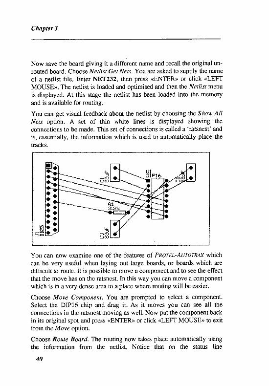
You can get visual feedback about the netlist by choosing the Slww All
Nets option. A set of thin white lines is displayed showing the
connections to be made. This set of connections is called a 'ratsnest' andis, essentially, the information which is used to automatically place the
tracks.
You can now examine one of the features of Pnorgt-Atnornur whichcan be very useful when laying out large boards, or boards which aredifficult to route. It is possible to move a component and to see the effectthat the move has on the ratsnest. In this way you can move a componentwhich is in a very dense area to a place where routing will be easier.
Choose Move Component. You are prompted to select a component.Select the DIP16 chip and drag it. As it moves you can see all theconnections in the ratsnest moving as well. Now put the component backin its original spot and press <ENTER>> or click <LEFT MOUSE>> to exitfrom the Move option.
Choose Route Board. The routing now takes place automatically usingthe information from the netlist. Notice that on the status line
40
tttt(}tf]
fL,srS"l13
Tutoriat: LaYing out a PCB
information is provided about the type of connection being made. This is
described in more detail in the routing chapter.
Connecting to power and ground planesThe final connections you have to make are to the power plane and
ground plane. pin 7 on the DB25 connector and pin 15 on the DIPI6
chip have tro be connected to the ground plane. Pin 16 on the DIP16 has
to be connected to the power plane. (This is assuming, of course, that
you are going to constrult u board with power and ground planes.)
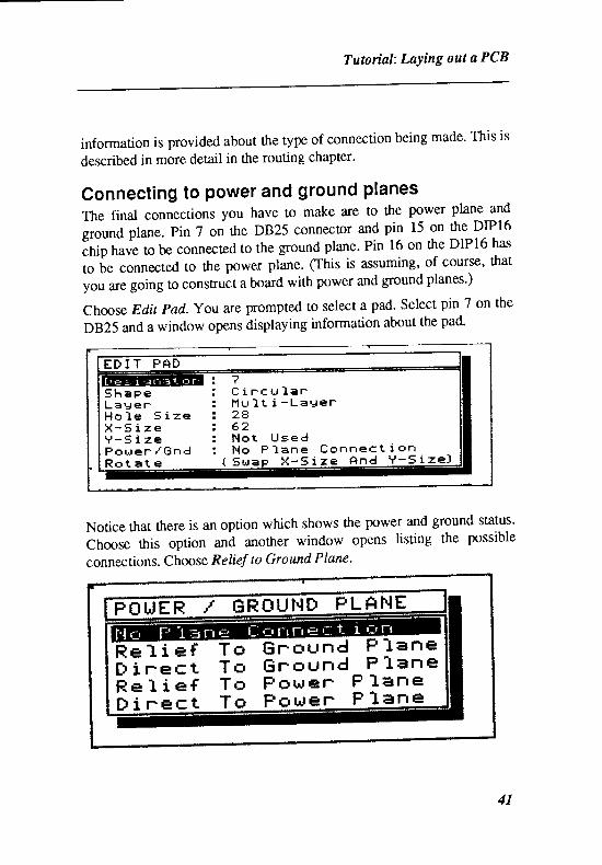
choos e Edit pad. you ue prompted to select a pad. select pin 7 on the
DB25 and a window opens displaying information about the pad.
E D I T P A D
S h a p eL a U e rH o l e 5 i z eX - 5 i z eY - 5 i z ePo r^ re r , r 'GndR o t e t e
7C i r c u f a rl " l u 1 t i - L a u e r2 S6 2l . { o t U s e dN o F ] a n e C o n n e c t i o n
( 5 r , r a p X - 5 i z e H n d V : 5 : L - z e l
Notice that there is an option which shows the power and ground status.
Choose this option and another window opens listing the possible
connections. Choose Relief to Ground Plane.
PL ffl.I.E
t - c r u n d P l e n eD i r e c t T o E r o u n d P l e n en e 1 i e f T o P o w e r F l e n eD i r e c t T o F o q s r F L e n e
4I

Chapter 3
Press <(ESC>) or click <RIGHT MOUSE>> and you are prompted to selectanother pad. Now choose pin 15 on ttre DIP16 and make ttre sameconnection. Finally, choose pin 16 on the DIPI6 chip and connect it tothe power plane by choosing the Relief to Power Plane option.
You have now completed ttre section of the board shown in the firstdiagram in this chapter. If you want to save your work, choose File Sm,eand enter a filename. Press <ENTER>> or click <LEFT MOUSE> and thefile is saved to the disk.
42
4 rurffig,fFfif$o NEW
In this tutorial you will learn how to create you own component pattrorn
and how to store the pattern in the library for later use. You may not
need to do this for a while because a comprehensive library of
component patterns is supplied with the Pn orru-AurorRfi{ package. In
addition, many components can be created by simply altering existing
library patterns using the Library Explode option.
Nevertheless, you will also learn other skills which will help you
become more familiar with the procedure for laying out a board.
The skills you will learn will be:
how to use the snaP grid;
relating cursor movement to the snap gnd;
laying tracks of a grven length;
creating new pad types;
changing the culrently selected pad type;
placing pads;
using the Repeat oqtions;
placing arcs;
defining a block;
creating a new library;
adding a component to the library.
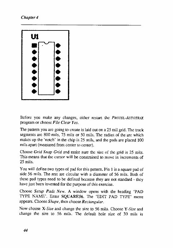
Getting startedThe component that you are going to create in this tutorial is a simple
DIpl6 pauern (which is already in the standard library - but the exercise
is useful).
43
Chapter 4
t ttotooolo
otaolooo
Before you make any changes, either restart the Pnornt-Awornurprogram or choose File Clear Yes.
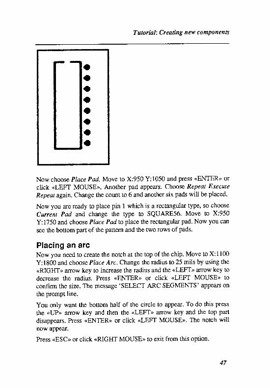
The pattern you are going to create is laid out on a 25 mil grid. The tracksegments are 800 mils, 75 mils or 50 mils. The radius of the arc whichmakes up the 'notch' in the chip is 25 mils, and ttre pads are placed 100mils apart (measured from center to center).
Choose Grid Snap Grid and make sure the size of the grid is 25 mils.This means that the cursor will be constrained to move in increments of25 mils.
You will define two types of pad for this pattern. Pin I is a square pad ofside 56 mils. The rest are circular with a diameter of 56 mils. Both ofthese pad types need to be defined because they are not standard - ttreyhave just been invented for the purpose of this exercise.
Choose Setup Pads New. A window opens with the heading 'PAD
TYPE NAME'. Enter SQUARE56. The 'EDIT PAD TYPE' menuappears. Choose Slnpe, lhen choose Rectangular.
Now choose X-Size and change the size !o 56 mils. Choose Y -Size andchange the size to 56 mils. The default hole size of 30 mils is
44
Tutorial: Creating new com7onents
satisfactory.Press <ESC> or click <RIGHT MOUSE>> to exit this option.
The square pad is now defined.
Repeat the procedure and define a pad called ROUND56 which is
circular wittr a diameter of 56 mils and also a hole size of 30 mils.
Remember to press <ESC>> or click <RIGHT MOUSE> nvice to exit this
option.
The next step is to make sure that the circular pad called ROUND56 is
the currently selected pad and that the track width is set to 12 mils.
Choose Current Pad Type and select ROLIND56. Also check that the
track width is l2 mils.
You are now ready to start creating the component.
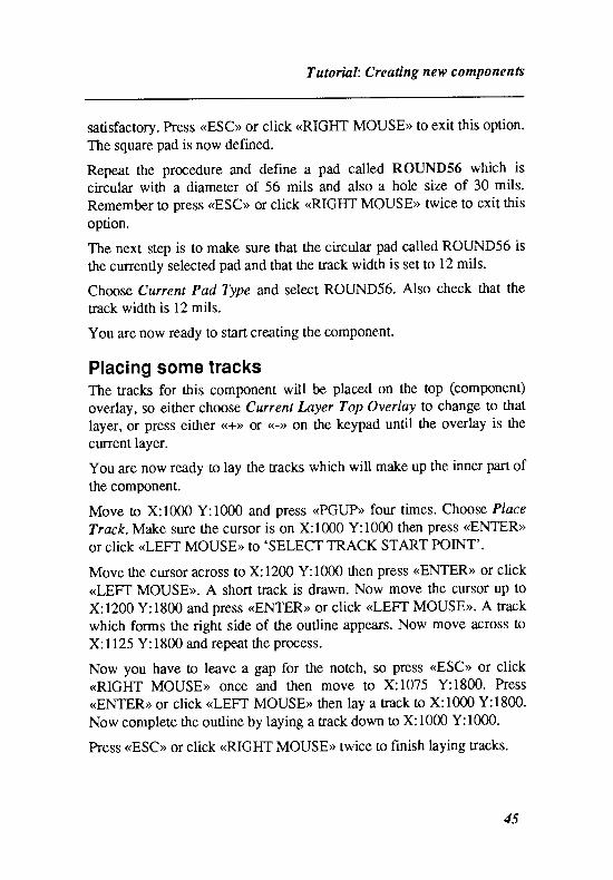
Placing some tracksThe tracks for ttris component will be placed on the top (component)
overlay, so either choose Current Layer Top Overlay to change to that
layer, or press either <<+>> or >
curent layer.
You are now ready to lay the tracks which will make up the inner part of
the component.
Move to X:1000 Y:1000 and press <PGUP> four times. Choose Place
Track.Make sure the cursor is on X:1000 Y:1000 then press <<ENfER>
or click (<LEFT MOUSE> to 'SELECT TRACK START POINT'.
Move the cursoracross to X:1200 Y:1000 then press <ENTER>> or click
<LEFT MOUSE>>. A short track is drawn. Now move the cursor up to
X:1200 Y:1800 and press <<ENIER>> or click <<LEFT MOUSE>>. A track
which forms the right side of the outline appears. Now move across to
X:1125 Y:1800 and repeat the process.
Now you have to leave a gap for the notch, so press <ESC> or click<RIGHT MOUSE> once and then move to X:1075 Y:1800. Press(ENTER>> or click <LEFT MOUSE> then lay a track to X:1000 Y:1800.
Now complete ttre outline by laying a track down to X:1000 Y:1000.
Press (ESC> or click <RIGHT MOUSE> twice to finish laying tracks.
45
Chapter 4
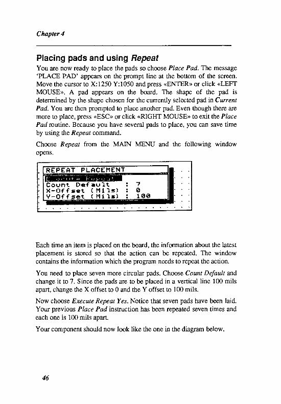
Placing pads and using RepeatYou are now ready to place the pads so choose Place Pad. The message'PLACE PAD' appears on the prompt line at the bottom of the screen.Move the cursor to X: 1250 Y:1050 and press <<ENTER>> or click <LEFTMOUSE>>. A pad appears on the board. The shape of the pad isdetermined by the shape chosen for the currently selected pad in CurrentPad. You are then prompted to place another pad. Even though there aremore to place, press <ESC>) or click <RIGHT MOUSE>> to exit the PlacePad routine. Because you have several pads to place, you can save timeby using the Repear command.
Choose Repeat from the MAIN MENU and the following windowopens.
R E P E f i T P L A C E I ' I E H T
C o u n t D e f e u l t :H - O f f s e t ( l ' f i l s ) :Y - O f f s e t ( 1 ' l i l s l :
7gr a 6
Each time an item is placed on the board, the information about the latestplacement is stored so that the action can be repeated. The windowcontains the information which the program needs to repeat the action.
You need to place seven more circular pads. Choose Count Defaulr andchange it to 7. Since the pads are to be placed in a vertical line 100 milsapart, change the X offset to 0 and the Y offset to 100 mils.
Now choose Exccute Repeat Yes. Notice that seven pads have been laid.Your previous Place Pad instruction has been repeated seven times andeach one is 100 mils apart.
Your component should now look like the one in the diagram below.
46
Tutorial; Creating new components
aaoattae
Now choose Place Pad. Move to X:950 Y:1050 and press <ENTER>> or
click <LEF f MOUSE>). Another pad appears. Choose Repeat Execute
Repear again. Change the count to 6 and another six pads will be placed.
Now you are ready to place pin I which is a rectangular type, so choose
Current Pad and change the type to SQUARE56. Move to X:950
Y:1750 and choose Place Pad to place the rectangular pad. Now you can
see the bottom part of the pattern and the two rows of pads.
Placing an arcNow you need to create the notch at the top of the chip. Move to X:1100
Y:1800 and choose Place Arc. Change the radius to25 mils by using the<RIGHT>> arrow key to increase the radius and the <<LEFT>) alrow key to
decrease the radius. Press <ENTER>> or click <LEFT MOUSE> to
confirm the size. The message 'SELECT ARC SEGMENTS' appears on
the prompt line.
You only want the bottom half of the circle to appear. To do this press
the <<UP>> arrow key and then the <LEFT> arrow key and the top part
disappears. Press <ENIER>> or click <<LEFIT MOUSE>>. The notch will
now appear.
Press (<ESC>) or click <RIGHT MOUSE>> to exit from this option.
47
Chapter 4
You are almost ready to add the component to the library. The only
remaining task is to assign the pin numbers or designators. The
rectangular pin will be pin 1, the one under that will be pin 2, and so on.
The pin in the top right hand corner will become pin 16.
Choose Edit Pod and then select the rectangular pad. Now choose
Designator and assign the value 1. Press <ESC>) or click <RIGHT
MOUSE>>. Now select each of the remaining pads and assign their
designators.
Adding the component to the l ibraryThe next step is to define the new component as a block by choosing the
Block Define option. When you choose the option the message'SELECT FIRST CORNER' appears on the prompt line at the bottom of
the screen. Move the cursor to X:850 Y:1900 and press <ENTER> or
click <LEFT MOUSE>>.
Now the prompt changes to 'SELECT SECOND CORNER'. Move the
cursor to X:1350 Y:950 and press <ENTER>> or click <LEFT MOUSE>>.
The component should now be highlighted indicating that it is a defined
block. The prompt 'SELECT REFiERENCE POINT' is now displayed
on the prompl line. The reference point is that part of t]re component that
will be placed at the cursor position during a later Place Component
operation. Choose the center of the rectangular pad (i.e. pin l) as the
reference point.
Since you probably do not want to add this component to your standard
library, create a new library trr store the component in. Choose Library
New Library and enter the name NEW for the library.
Now choose Library File and nominate NEW as the currently selected
library. You can check that it is the curently selected library by
choosi ng I nformation S tat us .
Choose l-ibrary Add. You are asked to enter a name for the new
component. Enter a name and then press (<ENTER>) or click <LEFT
MOUSE>>. Choose Yes. The component is added n the library.
If you now choose Library List you witl see the component listed. It can
now be placed on the board just like any other library component.
48
5 TUTORIAL: USING THE LINE EDITOR
The pnorrt-Awornm package contains a simple, yet effective, line
editor which is available in all input windows.
you will have already used an input window when you loaded ttre
DEMO file in a Previous httorial.
you can use tfie line editor to change text and to correct errors which
may arise when typing information into an input window.
This section contains a short tutorial to help you become familiar with
the line editor and a summ Ny of the functions available.
The skills you will learn will be:
using an input window;
deleting text at the cursor;
inserting text at the cursor;
moving around the window;
deleting an entire word or line;
exiting from an inPut window.
49
Chapter 5
The input window explainedThe first point to note is that when an input window opens it may alreadyhave some information on the edit line. This may either be a 'default'
specification such as *.PCB or DIP40 or a question mad<.
If a default specification or a question mark appears then clicking(<LEFT MOUSE>> or pressing <ENTER>> will cause a selection windowto open. The window will contain some names. One of these can beselected by moving the selection bar to that name and then clicking<<LEFT MOUSE>> or pressing <ENTER>>. This procedure overcome theneed for you to type information.
Whenever the window fint opens, the cursor appears on the left handside of the edit line. If you want to type a filename or the name of acomponent rather than selecting one from a list then simply type thename and any text that was already in the window will disappear.
You may sometimes make a typing error when entering a filename or acomponent designator. Alternatively, you may simply want trr make aminor change to the default value already in the window. This is wherethe line editor can help.
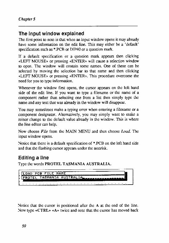
Now choose File from ttre MAIN MENU and then choose Load. Theinput window opens.
Notice that there is a default specification of *.PCB on the left hand sideand that the flashing cursor appears under the asterisk.
Edit ing a l ineType the words PROTEL TASMANIA AUSTRALIA.
L O A D P C B F I L E N A 1 ' 4 E
P R O T E L T A 5 1 ' I A N I A A U S T R A L I
Notice that the cursor isNow type <<CTRL> <A>>
50
positioned after the A at the end of the line.twice and note that the cursor has moved back
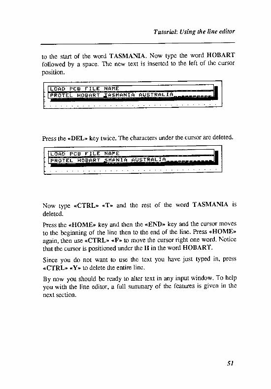
Tutorinl: Using the line editor
to the start of the word TASMANIA. Now type
followed by zt Sp?co: The new text is inserted to
position.
L O A D P C B F I L E N A H E
P R O T E L - I T O E N E T
J A S I " I A N I A A U S T R A L I A
Press the <DEL> key twice. The characters under the cursor are deleted.
L O A D P C B F I L E N A I ' 4 E
S H A N I A A U s T R A L I A
Now type <CTRL> <T> and the rest of the word TASMANIA is
deleted.
press the <HOME> key and then ttre ..END> key and the cursor moves
to the beginning of the line then to the end of ttre line. Press <HOME>
again, then use <CTRL> <F> to move the cursor right one word. Notice
that the cursor is positioned under the H in the word HOBART.
Since you do not want to use the text you have just typed in, press
<CTRL> <Y> to delete the entire line.
By now you should be ready to alter text in any input window. To help
you with the line editor, I full summary of the features is given in the
next section.
the word HOBARTthe left of the cursor
5I
Chapter 5
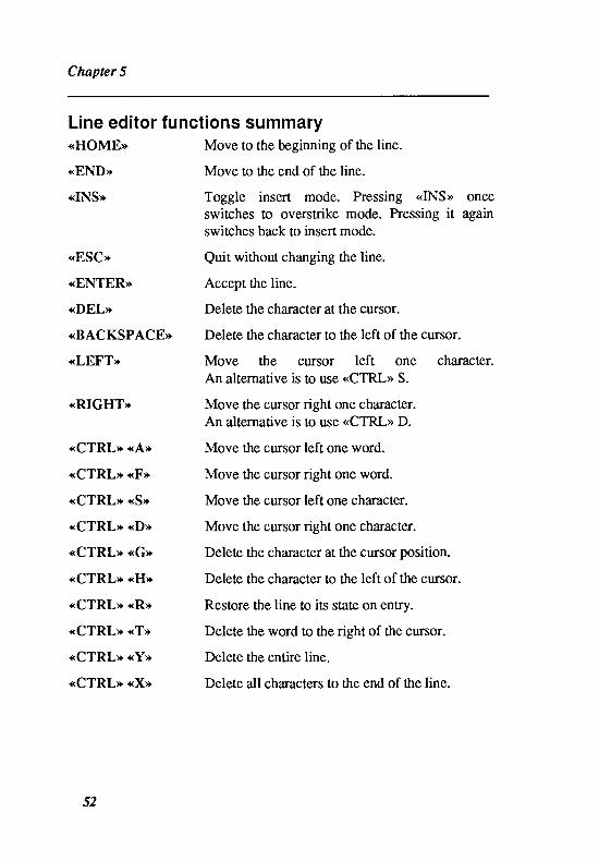
Line editor functions summary.<HOME> Move to the beginning of the line.
<<END> Move t,o the end of the line.
<INS> Toggle insert mode. Pressing <<INS>> onceswitches to overstrike mode. Pressing it againswirches back to insert mode.
<<ESC> Quit without changing the line.
<ENTER> Accept the line.
<DEL> Delete the character at the cursor.
<BACKSPACE> Delete the character to the left of the cursor.
(LEFT> Move the cursor left one character.
<RrcHr> ilffiffi{;ffiffi;'<CTRL> <A> Move the cursor left one word.
<CTRL> <F> Move the cursor right one word.
<CTRL> (S> Move the cursor left one character.
<<CTRL> <D> Move the cursor right one character.
<<CTRL> <G> Delete the character at the cursor position.
<CTRL> <H> Delete the character to the left of the cursor.
<CTRL> <R> Restore the line to its state on entry.
<CTRL> <T> Delete the word to the right of the cursor.
<CTRL> <<Y> Delete the entire line.
<CTRL> <X> Delete all characters to the end of the line.
52

6 TUToRIAL: AsstcNtNc KEY MAcRos
A powerful, and very useful, feature of Pnorg,t-AworRu( is the abitityto define your own macros. If you have not heard the term macro beforethen don't worrlr. It is simply a terrn that is used to describe a method ofassigning commonly used keystrokes to a single name or key.
The use of macros helps !o speed up operations that you need to carry
out often.
In this nrtorial you will learn the following skills:
clearing previously assigned macros;
defining a new macro;
assigning a macro name;
assigning a macro to a function key;
implementing a macro;
using the record facility to define a macro;
terminating the record facility;
saving a macro;
creating nested macros.
Defining a macroAn example will help. When laying out a board you will need to swapfrom the top layer to the bottom layer from time to time. One way of
doing this is by choosing Current from the MAIN MENU, then choosingLayer Bottom Layer.If you use single keystrokes you would fype C LB .
Before starting this tutorial you should make sure that there are nomacros already defined. Choose Setup Keys Clear Yes to clear anymacros from the memory.
53
Chapter 6
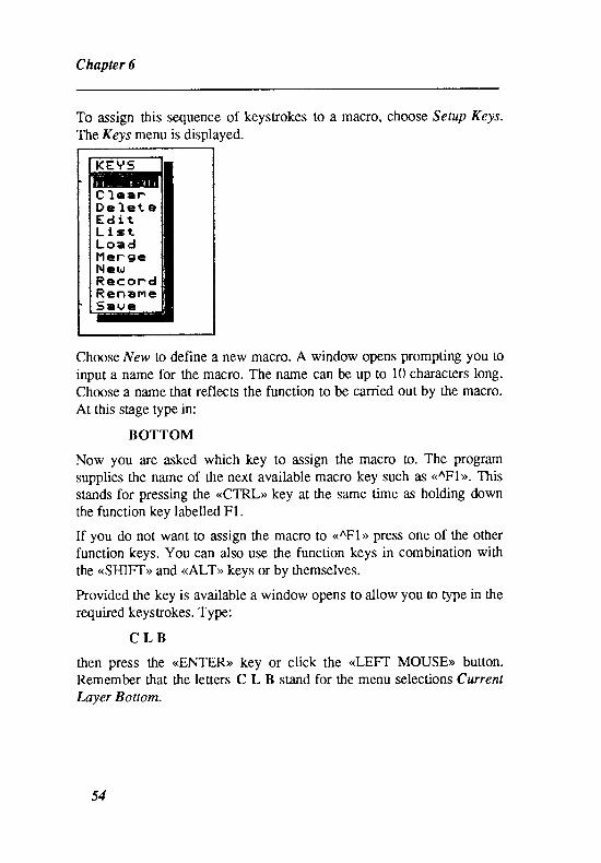
To assign this sequence of keystrokes to a macro, choose Setup Keys.
The Keys menu is displayed.
C l c r rD e l € t eE d i tL I s tL o a dJ ' le r geNeu lR e c o r dR e n e H e5 a v e
Choose New to define a new macro. A window opens prompting you toinput a name for the macro. The name can be up to l0 characters long.Choose a name that reflects the function to be carried out by the macro.At this stage type in:
BOTTOM
Now you are asked which key to assign the macro to. The program
supplies the name of the next available macro key such as <<nFl>>. Thisstands for pressing the <CTRL>) key at the same time as holding downthe function key labelled Fl.
If you do not want to assign the macro to <<^F1>> press one of the otherfunction keys. You can also use the function keys in combination withthe <SHIFT> and <ALT>> keys or by themselves.
Provided the key is available a window opens to allow you to type in therequired keysFokes. Type:
C L B
then press the <<ENTER>> key or click the <<LEFT MOUSE> button.Remember that the letters C L B stand for ttre menu selections CurrentLayer Bottom.
54
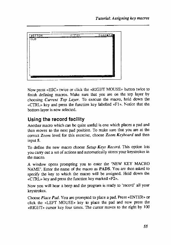
Tutorial: Assigning key macros
Eor- rcH {^F t> cor . r ra lC L B
Now press <<ESC>) twice or click the <RIGHT MOUSE> butfon twice to
finish defining macros. Make sure that you are on the top layer by
choosing Crrrent Top Layer. To execute the macro, hold down the
<CTRL> key and press the function key labelled (Fl>>. Notice that the
bottom layer is now selected.
Using the record facilityAnother macro which can be quite useful is one which places a pad and
then moves to the next pad position. To make sure that you are at the
correct Zoom level for this exercise, choo se Zoom Keyboard and then
input 5.
To define the new macro choose Setup Keys Record. This option lets
you carry out a set of actions and automatically stores your keystrokes in
the macro.
A window opens prompting you to enter the 'NEW KEY MACRO
NAME'. Enter the name of the macro as PADS. You are then asked to
specify the key to which the macro will be assigned. Hold down the(CTRL> key and press the function key marked (<F2>>.
Now you will hear a beep and the pro$am is ready to 'record' all your
keystrokes.
Choose Place Pad. You are prompted to place a pad. Press <ENTER>> or
click the <LEIT MOUSE> key to place the pad and now press the<RIGI{T>> cursor key four times. The cursor moves to the right by 100
55
Chapter 6
mils. Press <<ESC> or click the <RIGHT MOUSE> button to exit from
the Place Pad option.
Now, hold down the <CTRL>> key and press the <<END>> key. This turnsoff the 'recorder' and signifies that you have finished the macro.
Now press <<CTRL>> <<F2>>. Notice that a pad has been placed and the
cursor has moved !o a new position ready to place another pad. Press<CTRL>> <<F2>> again and notice that another pad has been placed.
Using nested macrosA powerful feature of macros is that one can call another. This is
sometimes referred to as 'nesting' macros.
An example for you to ry is creating a pin array consisting of four rows
of pads each of which has five pads. You should make sure that the pad
laying macro which you assigned to <CTRL>> <<F2>> is still there.
Choose Setup Keys New and input the name Line. You are prompted tosupply the name of the function key. Overwrite the default value bytyping <CTRL> <<F3>> then pressing <<ENIE,R>> or clicking <LEFT
MOUSE>>.
In the macro window type (<CTRL>> <<F2>> five times. This produces aline of five pads. Then press <DOWN>) (<DO'WN>) <LEFT> <<LEFT>)(<LEFT>) <<LEFT>> <LEFT>) (<LEFT>> <<LEFT> (<LEFT>> (<LEFT>) (<LEFT>)
to return the cursor to a point below the first pad. Terminate this macrodefinition by pressing <ENTER>> or clicking <<LEFT MOUSE>>.
Now define another macro and call it Array. Assign this definition to(<CTRL>) (<F4>>. Now press (<CTRL>) (F3>) four times. Terminate thedefinition by pressing <ENTER>> or by clicking <<LEFT MOUSE>>.
Now press <<ESC> twice to return to the PCB. Pick a blank area on theboard and press <<CTRL>) (<F4>). The macro executes automatically andlays down the array of pads.
s6
7 ruro RrA tbHt'dffnf t rRAxP Lor
This tutorial wilt show you how to do a simple draft print and a plot of
the sample pCB file. Pnorrt-Avrornur has a flexible set of output
routines which allow output fo be sent to draft printers, plotters,
photoplotters and disk files.
In this tutorial you will learn the following skills:
loading the TRNQLOT Program;
interpreting ttre menu levels;
interpreting the status screen;
loadirig a .PCB file;
interpreting the I nformation window;
setting up the parameters for a print;
setting up the parameters for a plot;
producing a draft Print;
producing a draft Plot.
Starting the ProgramIf you are using a dual floppy disk system, put the Plor disk into drive A:
and ttre disk with the .PCB file that you want to print into drive B:.
If you are using a hard disk drive you should make stue that you are in a
directory from which theTRNQLOT progam is accessible.
To start the TRilGLOT program simply type:
TRAXPLOT then Press <<ENTER>>
at the DOS PromPt.
57

Chapter 7
You will see the following menu.
NRIH PIOT NEHU
F i l eInf ornationOptionsSetupPlotPrlntGerber PlotlfC llri I I
The MAIN PLOT MENU is displayed on ttre left side of the screen and astatus window is displayed at the bottom of the screen.
Choose File Load and enter the file name DEMO in the input window.An information window opens showing the number of pads, tracks,components, etc. that are being loaded. A second pass shows thepercentage of the board which has been analysed.
When the file has been loaded, the status screen is updated to show thename of the .PCB file, the dimensions of the board and the amount offree memory remaining. The path name of ttre directory is alsodisplayed.
path : C:\pL$IIagurt File : ROGERZ.PCBlasrut Size | 2675 x 2560Free f1enory : 8929
The File menu is still displayed. Press <ESC> or click <RIGHTMOUSE>> to return to ttre MAIN PLOT MENU.
58
Tutorial: Using the TRAXPLOT program
A draft printNow choose Options Type of Ptor and choose Check Plot from the'select plot Tpe' window. Also check that the options selected for
border, pads and strings are 'on'. Press <ESC> or click <RIGHT
MOUSE>> to exit from this menu.
I-ets assume that you have an I{P Laser Jet II printer connected to a
serial port of your comPuter.
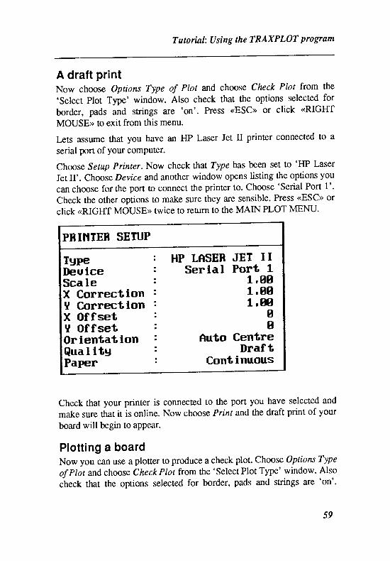
Choos e Setup Printer. Now check that Type has been set to 'I{P Laser
Jet II'. Choo se Device andanother window opens listing the options you
can choose for the port to connect the printer to. Choose 'serial Port 1'.
Check the other options to make sure they are sensible. Press <ESC>> or
click <RIGHT MOUSE>> twice to return to the MAIN PLOT MENU.
PRIHTER SETUP
TupeIfeu iceScaleX CorrectionI CorrectlonX OffsetY OffsetOrlentat lontlual ltgPaper
HP tfiSER JET IISer la I Port 1
T , B B1 ' B B1 . B B
IB
fiuto CentreIlraf t
Continuous
Check that your printer is connecrcd to the port you have selected and
make sure that it is online. Now choose Print and the draft print of your
board will begin to aPPear.
Plotting a boardNow you can use a plouer to produce a check plot. Choow Optiotrs Type
of ptot and choose Check PIot from the 'select Plot Type' window. Also
check that the options selected for border, pads and strings are'on'.
s9

Chapter 7
Press <<ESC>> or click <RIGHT MOUSE>> to exit from this menu.
Let's assume that you have a DMPL plotter connected to a serial port ofyour computer. (If you haven't, then choose from the list provided inSetup Plotter Type).
Choose Setup Plotter. Now check that Type has been set to 'Dlv{PL'.
Choose Device and another window opens listing the options you canchoose for the prt to connect the printer to. Choose 'Serial Port I' bymoving the selection bar to that option then pressing (<ENTER> orclicking <LEFT MOUSE>>. Check the other options to make sure theyare sensible. Press <<ESC>> or click <RIGHT MOUSE> trvice to return tothe MAINPLOTMENU.
PLOTTER SETUP
TgpeIleu iceScaleX ComectionY CorrectionX OffsetT OffsetOrientationQua I itgtFens
DNPtSerial Port 1
1 . B B1 . B B1 , B B
BB
llorna IIlraf t
If you now choose lrdormation, a window opens which provides youwith information about the plot type, the scale and the size of the board.You cannot change anything in this window - it is for information only.Press <ESC> or click <RIGHT MOUSE>> to exit from this window.
If you are happy with the setup oplions, choose Plot from the MAINPLOT MENU and your check plot will appear on the plotter.
60

7 ruro RrA tbHt'dffnf t rRAxP Lor
This tutorial wilt show you how to do a simple draft print and a plot of
the sample pCB file. Pnorrt-Avrornur has a flexible set of output
routines which allow output fo be sent to draft printers, plotters,
photoplotters and disk files.
In this tutorial you will learn the following skills:
loading the TRNQLOT Program;
interpreting ttre menu levels;
interpreting the status screen;
loadirig a .PCB file;
interpreting the I nformation window;
setting up the parameters for a print;
setting up the parameters for a plot;
producing a draft Print;
producing a draft Plot.
Starting the ProgramIf you are using a dual floppy disk system, put the Plor disk into drive A:
and ttre disk with the .PCB file that you want to print into drive B:.
If you are using a hard disk drive you should make stue that you are in a
directory from which theTRNQLOT progam is accessible.
To start the TRilGLOT program simply type:
TRAXPLOT then Press <<ENTER>>
at the DOS PromPt.
57

Chapter 7
You will see the following menu.
NRIH PIOT NEHU
F i l eInf ornationOptionsSetupPlotPrlntGerber PlotlfC llri I I
The MAIN PLOT MENU is displayed on ttre left side of the screen and astatus window is displayed at the bottom of the screen.
Choose File Load and enter the file name DEMO in the input window.An information window opens showing the number of pads, tracks,components, etc. that are being loaded. A second pass shows thepercentage of the board which has been analysed.
When the file has been loaded, the status screen is updated to show thename of the .PCB file, the dimensions of the board and the amount offree memory remaining. The path name of ttre directory is alsodisplayed.
path : C:\pL$IIagurt File : ROGERZ.PCBlasrut Size | 2675 x 2560Free f1enory : 8929
The File menu is still displayed. Press <ESC> or click <RIGHTMOUSE>> to return to ttre MAIN PLOT MENU.
58

Tutorial: Using the TRAXPLOT program
A draft printNow choose Options Type of Ptor and choose Check Plot from the'select plot Tpe' window. Also check that the options selected for
border, pads and strings are 'on'. Press <ESC> or click <RIGHT
MOUSE>> to exit from this menu.
I-ets assume that you have an I{P Laser Jet II printer connected to a
serial port of your comPuter.
Choos e Setup Printer. Now check that Type has been set to 'I{P Laser
Jet II'. Choo se Device andanother window opens listing the options you
can choose for the port to connect the printer to. Choose 'serial Port 1'.
Check the other options to make sure they are sensible. Press <ESC>> or
click <RIGHT MOUSE>> twice to return to the MAIN PLOT MENU.
PRIHTER SETUP
TupeIfeu iceScaleX CorrectionI CorrectlonX OffsetY OffsetOrlentat lontlual ltgPaper
HP tfiSER JET IISer la I Port 1
T , B B1 ' B B1 . B B
IB
fiuto CentreIlraf t
Continuous
Check that your printer is connecrcd to the port you have selected and
make sure that it is online. Now choose Print and the draft print of your
board will begin to aPPear.
Plotting a boardNow you can use a plouer to produce a check plot. Choow Optiotrs Type
of ptot and choose Check PIot from the 'select Plot Type' window. Also
check that the options selected for border, pads and strings are'on'.
s9
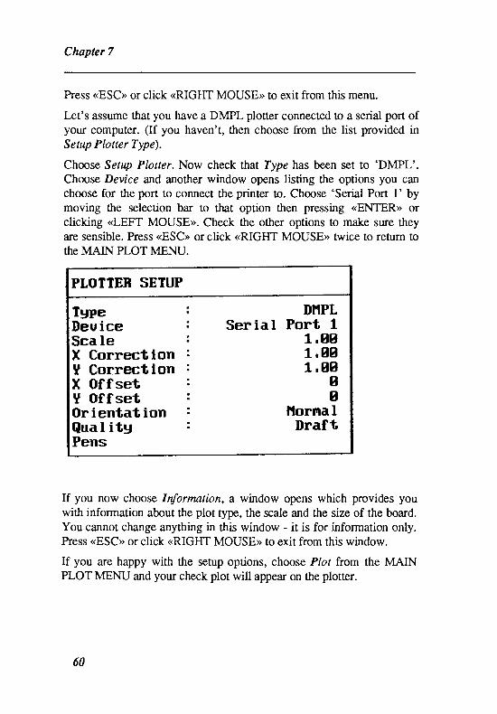
Chapter 7
Press <<ESC>> or click <RIGHT MOUSE>> to exit from this menu.
Let's assume that you have a DMPL plotter connected to a serial port ofyour computer. (If you haven't, then choose from the list provided inSetup Plotter Type).
Choose Setup Plotter. Now check that Type has been set to 'Dlv{PL'.
Choose Device and another window opens listing the options you canchoose for the prt to connect the printer to. Choose 'Serial Port I' bymoving the selection bar to that option then pressing (<ENTER> orclicking <LEFT MOUSE>>. Check the other options to make sure theyare sensible. Press <<ESC>> or click <RIGHT MOUSE> trvice to return tothe MAINPLOTMENU.
PLOTTER SETUP
TgpeIleu iceScaleX ComectionY CorrectionX OffsetT OffsetOrientationQua I itgtFens
DNPtSerial Port 1
1 . B B1 . B B1 , B B
BB
llorna IIlraf t
If you now choose lrdormation, a window opens which provides youwith information about the plot type, the scale and the size of the board.You cannot change anything in this window - it is for information only.Press <ESC> or click <RIGHT MOUSE>> to exit from this window.
If you are happy with the setup oplions, choose Plot from the MAINPLOT MENU and your check plot will appear on the plotter.
60

REIiEREI{CE SECTION

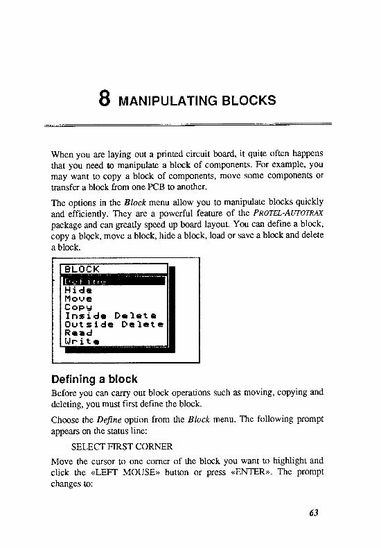
8 MANIPULATING BLocKs
When you are laying out a printed circuit board, it quite often happens
that you need to manipulate a btock of components. For example, you
may want to copy a block of components, move some components or
transfer a block from one PCB to another.
The options in the B/ ock menu allow you to manipulate blocks quickly
and efficiently. They are a powerful feature of the Pnornt-Avtornurpackage and can greatly speed up board layout. You can define a block,
copy a blqck, move a block, hide a block, load or save a block and delete
a block.
B L O C K
H i d el ' f oueC o P gI n s i d n D e l e t nB u t s t d e D e l e t eR e a dU n i t s
Defining a blockBefore you can carry out block operations such as moving, copying and
deleting, you must first define the block.
Choose the Define option from the Blocft menu. The following prompt
appears on the status line:
SELECT FIRST CORNER
Move the cursor to one corner of the block you want to highlight and
click the (<LEFT MOUSE> button or press <ENTER>). The prompt
changes t0:
63
Chapter I
SELECT SECOND CORNER
Move to the diagonally opposite corner and click the <<LEFT MOUSE>button or press <<ENTER>>.
The block is highlighted and the prompt:
SELECT REFERENCE POINT
appears.
The reference point is any point you decide tn choose [o assist you inmoving and placing the block. When you move or copy a block, it is thereference point which moves with the cursor. Some people make one ofthe corners the reference point, but it ls also possible to make the cornerof a particular component in the block a reference point. If you aremarking a block in order to create a library component, it is a good idea
to select the pad which will become pin I as the reference point. Thereference point can also lie outside the block.
If you want to define a new block and there is one already defined, don'tworry! Simply go ahead and define the new block and the previous blockis released.
' H i d i n g ' a b l o c kUse Block Hide when you want to take the highlight off a particular
block but do not want, to define a new block.
The Hide option simply removes the highlight from a block. You willnotice that the highlight disappears from the selected block once you
choose Hide indicating that the block is no longer defined..
Moving a blockOnce you have defined a block with Block Define, you can move it toanother place on the board.
Choose Block Move and the prompt
PLACE BLOCK
appears. You can now specify the new position for the block. Use themouse or ttre cursor keys to position the outline of the block in the
64
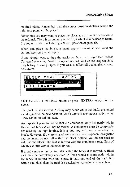
Manipulating blocks
required place. Remember that the cursor position dictates where the
reference point will be Placed.
Sometimes you may want to place the block at a different orientation to
the original. Thcre is a summary of the keys which can be used to rotate,
flip and move the block durin g a Move operation on page 66-
When you place the block. a menu appears asking if you want the
current layer only or all layers.
If you simply want to drag the tracks on the current layer then choose
Current Layer Only" With this option no pads or vias are dragged since
they belong to every layer. If you wish to affect all tracks, then choose
All Layers.
click the <LEFT MOUSE> button or press <ENTER> to position the
block.
The block is then moved. A delay may occur while the tracks are sorted
and dragged m the new posiuon. Don't worry if they appear to be messy- they can be sorted out later"
An important point to note is that if a component only lies partly within
the defined block it will not be moved. A component must be completely
enclosed by the highlighting. If it is not, you will need to redefine the
block. However, if the associated text such as the component designator
and comment do not fall within the block outline, you do not need to
redefine the block. The text is moved with the component regardless of
whether it falls within fte block or not.
If a pad centre or arc cenre falls within the block it is moved. A filled
area must be completely enclosed. A track which is completely within
the block is moved with the block. If only one end of the track lies
within that block then the track is stretched to maintain the connection.
6s
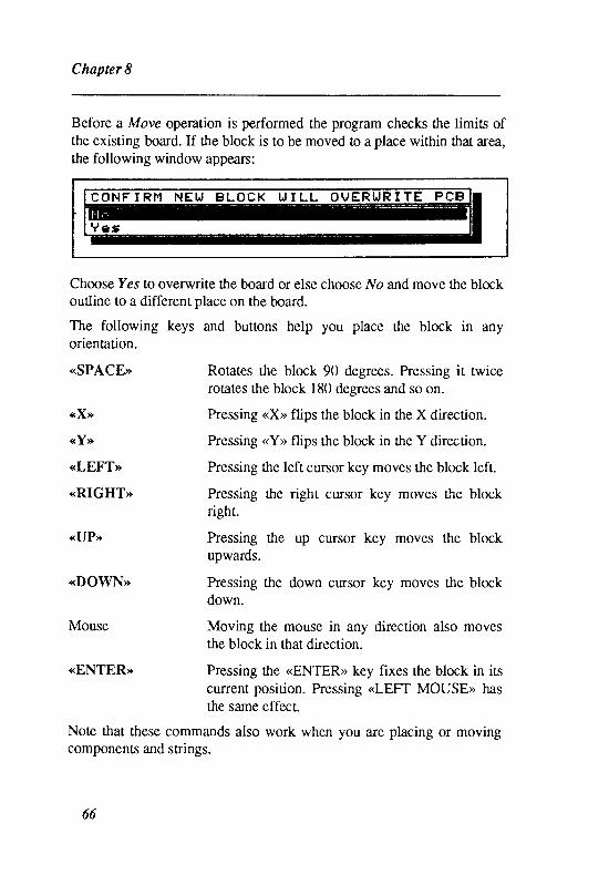
Chapter I
Before a Move operation is performed the program checks ttre limits ofthe existing board. If the block is to be moved to a place within that are*,,the following window appears:
Choose Yes to overwrite the board or else choose No and move ttre blockoutline to a different place on the board.
The following keys and buttons help you place the block in anyorientadon.
<SPACE> Rotates the block 90 degrees. Pressing it twicerotates the block 180 degrees and so on.
<X> hessing <<X>> flips the block in ttre X direction.
<Y> Pressing <<Y>> flips the block in the Y direction.
<LEFT> Pressing the left cursor key moves ttre block left.
<RIGHT> Pressing the right cursor key moves the blockright.
<UP> Pressing the up cursor key moves the blockupwards.
(DOWN> Pressing the down cursor key moves the blockdown.
Mouse Moving the mouse in any direction also movesthe block in that direction.
<ENTER> Pressing ttre <ENTER> key fixes the block in itscunent position. Pressing <LEFT MOUSE> hasthe same effect.
Note that these commands also work when you are placing or movingcomponents and strings.
66
Manipulating blocks
Copying a blockThe Copy option is similar to the Move option (see pages g-q with one
important difference. When a block is copied a new copy of each of the
components in the block is made and the original components remain.
The component designators are incremented to the next free value to
ensure that the new designator is unique.
Thus if the component with the designator U2 is copied, the new
component is given a new designator depending on the number of 'U'
designators already on the board. If there were alread;i the designators
Ul to U6, the copied component would be labelled U7.
Remember that when copying a block it is possible that you will
overwrite an existing part of ttre PCB. When you Copy a block, the new
block is highlighted and becomes the defined block.
Deleting a blockBefore you can delete a block you must first define it. See pages 63-4 for
a description on how !o define a block. Once it is defined, You can delete
everyttring in the defined area or everything outside the defined area.
Choose Block Inside Delete to delete everything inside the defined
block. Choose Block Outside Delete to delete everything outside the
detined block. In each case you are asked to confirm that you want to
delete the area. Choose Yes to confirrn, or lfo if you want, to change your
mind.
Care must be taken with block deletion commands. It is srongly
recommended that you save a copy of the file before attempting a
deletion.
One point to bear in mind when deleting outside a block is that a track
which passes completely through ttre defined block is also deleted. This
happens because the part of the track inside the block is simply a route
between connections which lie outside ttre block.
If you try to delete without having defined a block, the message:
BLOCK NOT MARKED
is displayed. You should then choose Block Define to define the block
you want to delete.
67
Chapter 8
Reading a blockSince there are common blocks of components that you may want to useon many boards, it is possible to store a number of componentconfigurations in separate .PCB files and then read them into the currentboard when you require them. You can identify a file stored on the disk,then merge it into the board you are working on in the computer'smemory.
To read a block, choose Block Read and specify the name of the .PCBfile. The prompt 'PLACE BLOCK' appears. You are asked to confirmthe fact that you want to load a .PCB file. ChooseYes to load the file.
Move the block outline until it is in ttre position you require. Rememberto use <SPACE>>, <<X>) and (<Y>) to rotate or flip the block, then click<LEFT MOUSE>> or press <ENTER>).
The block which is loaded remains as a defined block until you chooseBlock Hifu or else define another block.
Saving part of a layoutIf you identify part of a current layout as a block you might want to useon another occasion, it is a good idea to save it on a disk iN a separatefile.
To do tttis, define the section of the layout as a block using the BlockDefine option. Then, choose BlockWrite. You are prompted to supply a.BLOCKWRITE FILE NAME"
Enter a filename. If the filename you enter does not exist, ttre block iswritten out to that file. If it already exists, you are asked to confirm thatyou want to ovenvrite the file. If you do want to overwrite the filechoose Yes, if not choose No then repeat the process with a differentfilename.
68
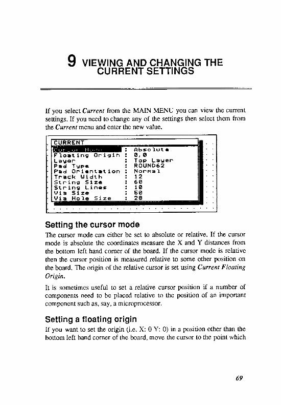
I vrEWrNG AND cHANGING THECURRENT SETTINGS
If you select Currenr from the MAIN MENU you can view the current
settings. If you need to change any of ttre settings then select them from
the Current menu and enter the new value.
C U R R E N T
F l o a t i n g O n i g i nL a u e nP a d T u p eP a d O n i e n t r t i o nT n a c l c U t d t hS t n i n g S i z eS t n i n g L i n e sU i a 5 i z eU i a H o l c S i z e
A b s o l u t rE r AT o p L a u e nR O U N D 6 2N o r n n a It 26 g1 g5 B2 B
Setting the cursor modeThe cursor mode can either be set to absolute or relative. If the cursormode is absolute the coordinates measure ttre X and Y distances from
the bottom left hand corner of the board. If the cursor mode is relative
then the cursor position is measured relative to some other position on
the board. The origin of the relative cursor is set using Current Floating
Origin.
It is sometimes useful to set a relative cursor position if a number ofcomponents need to be placed relative to the position of an important
component such as, say, a microprocessor.
Sett ing a f loat ing originIf you want to set the origin (i.e. X: 0 Y: 0) in a position other than thebottom left hand corner of the board, move the cursor to the point which
69
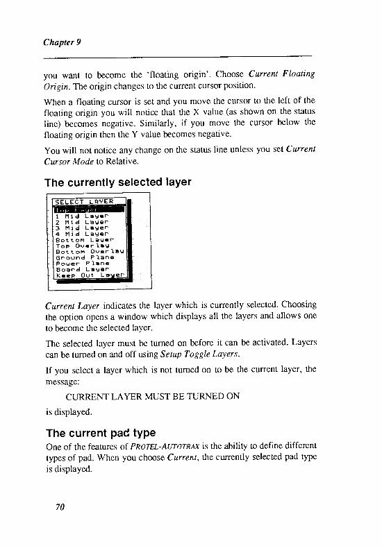
Chapter 9
you want, to become the 'floating origin'. Choose Current Floating
Origin The origin changes to the current cursor position.
When a floating cursor is set and you move the cursor to the left of the
floating origin you will notice that the X value (as shown on the status
line) becomes negative. Similarly, if you move the cursor below the
floating origin then the Y value becomes negative.
You will not notice any change on the status line unless you set Current
Cursor Mode to Relative.
The currently selected layer
S E L E C T L q I E E
I l ' l i d L a U r r2 l ' l i d L a u e r3 H i d L e u e r4 H i d L a s e rB o t t o n L e u e rT o p O v r n l , r UB o t t o n 4 O v e r l a gE n o u n d P l a n eP o r r r e r P l a n eB o a r d L e u e rK e e e O u t L a Y e r
Current Layer indicates the layer which is currently selected. Choosing
the option opens a window which displays all the layers and allows one
to become the selected layer.
The selected layer must be turned on before it can be activated. Layers
can be turned on and off using Setup Toggle Layers.
If you select a layer which is not turned on to be the current layer, ttre
message:
CURRENT LAYER MUST BE TURNED ON
is displayed.
The current pad typeOne of the features of Pnoru-Arnornur is the ability t,o define differenttypes of pad. When you choose Current, the curently selected pad typeis displayed.
70
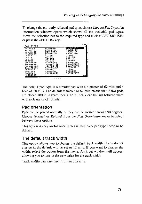
Vicwing and changing the current settings
To change the currently selected pad type, choose Current Pad Type. Aninformation window opens which shows all the available pad types.Move the selection bar to the required type and click <LEFT MOUSE>or press the <ENIER>> key.
P A D T Y P E S
R O U N D 4 A R O U N D S BR O U N D " 6 R O U N D A S R O U N D I a 6R O U N D I 2 5 R O U N D 1 5 8 R O U N D T 7 5R O U N D z B A R O U N D 2 2 5 R O U N D 2 E So c T 4 0 0 c T 5 6 0 C T 6 2o c T ? g o c r a s o c T l g oo c T I 2 5 o c T 1 5 g O C T I 7 5o c T z e � 8 � o c r 2 2 5 0 C T 2 5 gs O U f f R E s g 5 E U A R E 6 2 s O U A R E ? €5 O U A R E 8 5 S E U A R E I g g 5 A U A R E I 2 5s O U A R E l s A S E U A R E 1 7 5 5 O U A R E 2 A 65 8 U A R E 2 2 s 5 0 U A R E 2 S A R 5 g X 1 2 AR S S X 1 2 g D I P E A D I P A AE 5 S X 2 5 B E 5 S X 5 B 6 E 8 6 X ? 5 6E 8 6 X 5 A 6 E I 2 B X l 9 � 0 A T A R G E T 5 6 0t ' t o I R E 5 A 9
The default pad type is a circular pad with a diameter of 62 mils and ahole of 28 mils. The default diameter of 62 mlls meilns that if trvo padsare placed lm mils apart, then a 12 mil track can be laid between themwith a clearance of 13 mils.
Pad orientationPads can be placed normally or they can be rotated through 90 degrees.Choose Norm"a/ or Rotated from the Pad Orientation menu to selectbetween these options.
This option is very useful since it means that fewer pad types need to bedefined.
The default track widthThis option allows you to change the default track width. If you do notchange it, the default will be set to 12 mils. If you want tb change thewidth, select the option from the menu. An input window will appear,allowing you to type in the new value for the track width.
Track widths can vary from I mil to 255 mils.
7I
Chapter 9
Checking the text heightThe Current String Size option allows you !o change the height of thetext which appears on the board. The height can be changed at any [ime,but this option should be set to the size which you use most often.
Once again an input window will appear which will allow you to type inthe new value. Choose a value from 36 mils to 1000 mils.
Checking the width of str ing l inesThe width of the 'brush strokes' which make up the individual charactersin srings can be varied by choosing Current String Line.s. The normalvalue is l0 mils, but if you want a partrcular string to have moreemphasis then increase the string width to l5 or 20.
Make sure you choose a width which is compatible with the text height.For example, a width of l0 mils looks reasonable with a text height of 60mils, but a width of 30 mils makes the text illegible. However, a width of50 mils looks reasonable with & text height of 500 mils.
The width can vary from I mil to 255 mils.
The default via sizeThe default via size is 50 mils. This can be changed by selecting CurrentVia Size and then entering a new value in the input window.
Vias can vary in size from I to 255 mils. Be careful about making viastoo large as this will restrict the choices for the automatic router whenlaying racks.
The default via hole sizeThe via hole size is the diameter of the hole through the board. This mustobviously be less than the size of the via. The program checks to ensurethat a hole size is not specified greater than the via size. If it is larger, thehole size will be changed to a value which is I less than the via size.
Thus if the via size is 50 mils and a via holc size of 70 mils is specifiedthe hole sue wil l be automatically changed to 49 mils.
Choose Current Via llole Size to change from thc default value of 28mi ls"
72
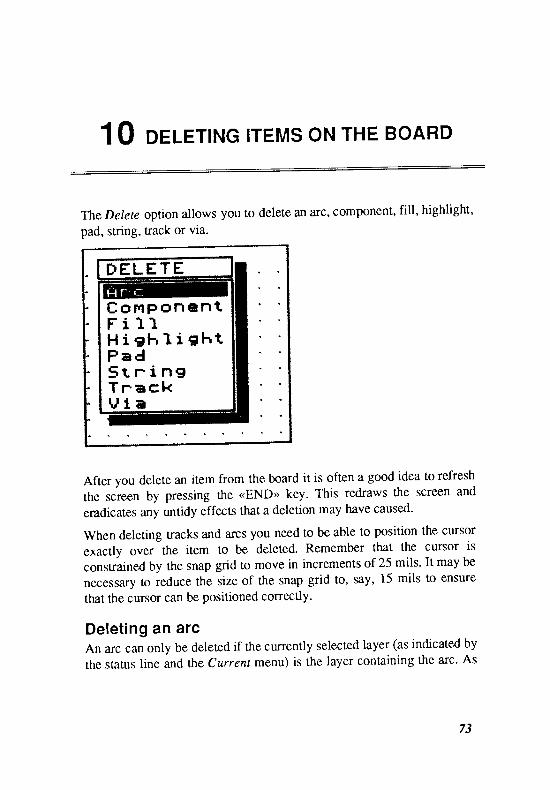
10 DELETTNG trEMs oN THE BoARD
The Delete option allows you to delete an arc, component, fill, highlight'
pad, string, track or via.
D E L E T E
C o n P o n e n tF i 1 , 1H i e h l i s h tP a d
i S t r i n gI f r e c kl U i a
After you delete an item from the board it is often a good idea to refresh
the screen by pressing the <END> key. This redraws the screen and
eradicates any untidy effects that a deletion may have caused.
When deleting tracks and arcs you need to be able to position the cursor
exactly over the item to be deleted. Remember that the cursor is
constrained by the snap gnd to move in increments of 25 mils. It may be
necessary !o reduce the size of the snap grid to, Soy, 15 mils tro ensure
that the cursor can be positioned correctly.
Delet ing an arcAn arc can only be deleted if the currently selected layer (as indicated by
the sratus line and the Current menu) is the layer containing the arc. As
73
Chapter I0
they are normally found on the component overlay, this layer should beselected before you attempt the deletion.
Choose Delete Arc and you are prompted tio select an arc. Move thecursor to anywhere on the arc to be deleted and click the <LEFTMOUSE> button or press <ENltR>>. You are asked to confirm that youwant to delete the highlighted arc. If you choose Yes the arc is deleted.
If you hear a beep or if the arc is not deleted you may need to do one oftwo things. First, check that you are on the correct layer. Second, makesure that the cursor is correctly positioned over the arc. If you find itdifficult to position the cursor you might have to change the size of thesnap grid,
Delet ing a componentYou can delete a component regardless of the currently selected layer.There is no need to change tro the component layer prior to deleting acomponent.
To delete a component choose Delete Component. You are prompted toselect a component. Use the mouse or the arrow keys to move to thecomponent you want to delete.
Now click (LEFT MOUSET, 61 press <ENTER>> to select the component.A window opens askrng you to confirm that you really do want to deletethe componenl Choose Y es and the component will be removed fromthe board.
If you click <LEFT MOUSE>> or press <ENTER>> when the cursor is notover a component, an input window opens asking you to input thecomponent designator. Enter the component designator of thecomponent you want. tro delete. Be careful, because you can delete acomponent that is not currently displayed on the screen!
Delet ing a f i l lAny fill area you want to delete must be on the currently selected layer.
To delete a fill, simply choose the Delete Fill option, move to therequired fill and confirm that it is the one you want to delete.
71
Deteting items on the board
Delet ing a highl ightIf you want to dele te aset of highlighted tracks you must first choose the
Hightight option from the MAIN MENU. Highlight the required tracks
as described in Chapter 14. It is rhen a good idea to choose Zoom All to
fit the board on the screen so that you can make sure that it has not
highlighred any tracks that you do not intend to be deleted.
Choose Delete Highlight and the highlighted section will be deleted.
Remember to press <END>> tro refresh the screen'
If you want to delere an exrcrnal plane then firstly choose Highlight Net
to highlight some or all of rhe plane" Then choose Delete Highlight to
delete it. you should be aware that an external plane may be broken into
many sections and hence you may necd to highlight each separately.
Note that deleting a highlight does nor delete any components.
Deleting a PadA pad can be deleted from any layer since it belongs to evsry layer.
Choose the Delete pad oprion and the prompt 'SELECT PAD' appears
on the status line. Move the cursor to the pad to be deleted and then
press <ENTERT> or click (LEFT MOUSE>). If the pad cannot be deleted
vou will hear a beep. If it can be deleted a window will appear asking
you to confirm that you want to delete the pad - and the pad will appear
in inverse. Choose Yes and the pad will bc deleted'
you will then be asked to select another pad. When you have finished
delering pads press the .,Esc" key or click <RIGHT MousE>-
Do nor t^ry to delere a pad which is part of a library component. You rteed
to delcte the entire component rather than just one pad'
Delet ing a str ingTo delete a string, you must be on the same layer as the string to be
deleted.
Choose the Delete String option and the prompt 'SELECT STRING' is
displayed. Move to the sning you want to delete then press <ENTER>> or
click the <LEFT MOUSE> butlon.
75
Chapter I0
The string to be deleted appears in inverse so that you can confirm that itis the one you want to delete. Choose Yes to confirm the deletion.
Deleting a trackNote that you must be on the same layer as the track you want to delete.
To delete a track (which is any snaight line part of a net) simply chooseDelete Track, then move the cursor to the track required and either clickthe <LEFT MOUSE> button or press (<ENTER>>. The track you havechosen appea$ in inverse and you are be asked to confirm that you wantto delete it. Choose Yes to delete it or Na to leave the track there. Press<<ESC> or click <RIGHT MOUSE> when you have finished deleringfracks.
If you cannot get ttre cursor to sit on the track you want to delete changethe snap grid size in the Grid option of the MAIN MENU ro a smallerfigure (e.g. from 25 down to 15 mils).
Deleting a viaA via can be deleted from any layer.
Choose Delete Via then move to the via to be deleted. The prompt'SELECT VIA' appears on the status line. If your view of the via is notclear enough, press <PGUP>> to expand the window.
Click the <LEFT MOUSE> button or press <<ENTER>> to delete the via.Press <ESC>> or click <RIGHT MOUSE> when you have finisheddeleting vias.
76
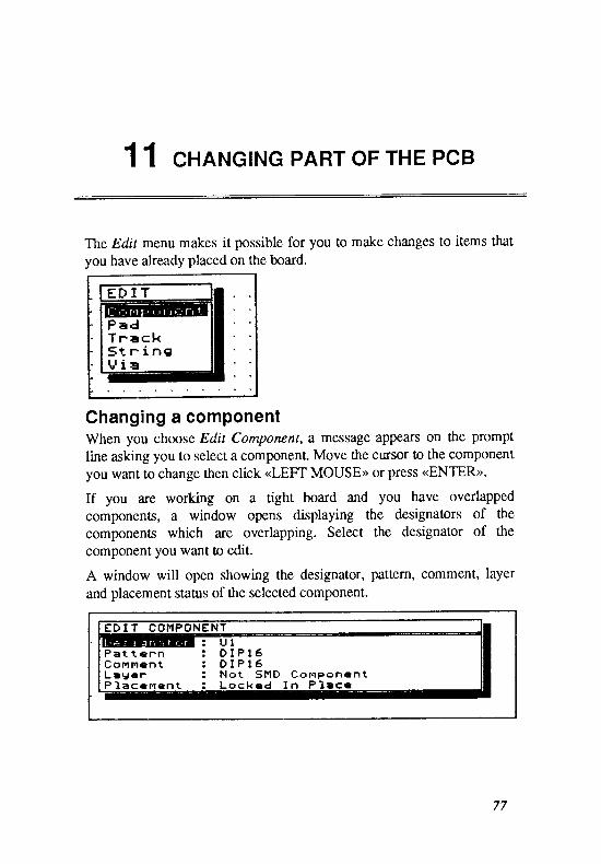
1 1 cHANGING PART oF THE PcB
The Edit menu makes it possible for you to make changes to items that
you have already placed on the board.
IlT::.x l l : :l : :
Changing a componentWhen you choose Edit Component, a message appears on the prompt
line asking you to select a component. Move the cursor to the component
you want to change then click <LEFT MOUSE>> or press <EN1ER>>.
If you are working on a tight board and you have overlapped
components, a window opens displaying the designators of the
components which are overlapping. Select the designator of the
component you want to edit.
A window will open showing the designator, pattern, comment, layer
and placement status of the selected component.
E D I T C O H P O N E N T
P a t t e r nC o m n r e n tL r U e rP l a c c m r n t
U 1D I P l 6D I P l 6N o t 5 1 ' l D C o m p o n e n tL o c k a d I n P l e c e
77

Chapter I1
You can change each of these by moving the selection bar to therequired option and pressing <ENTER> or clicking <LEFT MOUSE>. Ifyou choose to edit the component designator, a window will open
displaying four options.
C O H P C I N E I q T D E S I B ] { R T O RtI U 1
6 A1 BD i
5 iL iH i
Z E :n e :d e : g s p l a
You can change the text (e.9. change U3 to C4), the size of the text and
the width of the string lines. The final oprion allows you to hide or
display the designator. Normally, you would choose to display thedesignator, but if you are laying down a cluster of components which arethe same, you may only want to display the designator and comment for
one.
When you have finished editing the designator, click (RIGHT MOUSE>>
or press ..ESC> to return to the Edit Component menu.
Changing the Comment field is done in the same way as the designator.You should note that it is possible to choose a text height which causes
the comment string to overwrite the designator string.
You can change the layer if the component is a Surface Mount Device(SMD). SMDs belong to only one layer. They are glued to that layer -
they do not have pins mounted through the board.
Choose Edit Component Layer and a window opens asking you to selecteither the top layer or bottom layer for the component. If the componentis not an SMD, no action will be taken.
If you choose Edit Component Placement a window opens giving you
the option of choosing 'Free To Move' or 'Locked In Place'. This isimportant when components are being placed automatically. If you
assign 'Locked In Place' to a component, then it will not be moved to
78
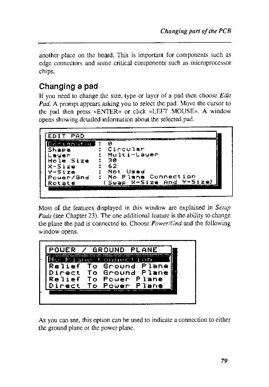
Changing part of the PCB
another place on the board. This is important for components such as
edge connectors and some critical components such as microprocessor
chips.
Changing a padIf you need to change the size, type or layer of a pad then choose Edit
Pad. A prompt appears asking you to select the pad. Move the cursor to
the pad then press <ENTER> or click <LEFT MOUSE>). A window
opens showing detailed information about the selected pad.
Most of the features displayed in this window are explained in SetupPads (see Chapter 23). The one additional feature is the ability to change
the plane the pad is connected to. Choose PowerlGnd and the followingwindow opens.
P O U E R / E R O U N D P L A F I E
R e 1 i e f T o G r o u n d P l e n eD i r e c t T o G r o u n d P l a n €R e 1 i e f T o F o w e r P l e n eD i F e c t T o P o u r r F l e n s
As you can see, this option can be used to indicate a connection to eitherthe ground plane or the power plane.
E D I T P A D
S h e p eL a \ J e rH o l e 5 i z eX - 5 i z eY - 5 i z eP o t ^ r e t / G n dR o t e t e
BC i r c u l a rl " l u l t i - La t l e r3 g6 2N o t U s e dN o P l , e n e C o n n e c t i o n
( 5 r ^ r a p X - S i z e H n d Y - - - 1 i z e J
79
Chapter I I
Choose the plane that the pad is to be connected to, then press <EI.ITER>
or click <LEFT MOUSE>>.
Changing a trackYou can change the layer a track is on or you can change the width of a
frack.
Choose Edit Track. A window opens allowing you to change the track
layer or the track width.
To change the layer, choose Layer. A window opens displaying all the
signal and overlay layers which are available. Choose the layer !o whichyou want 0o transfer the track then press <<ENTER>> or click <LEFT
MOUSE>>.
To change the track width, choose Width, select a track and input the
new width (remember that you must be on the same layer as the trackyou are trying no select). You are asked whether you want trl just change
the selected track, the highlighted tracks or all nacks on the board.
T C H I H G T R A g K - s I z E s
H i s h l i s h t e d T r e c k sA l l T n a c k s o n P C B
Be careful if you choose the second or third options, global changes to
track widths can lead to some unexpected problems.
Changing a str ingYou can change the style of a string or the characters which comprise the
string.
Choose Edit String and a window opens giving the following options.
80
A A A A
Changing part of the PCB
Choos e Size !o change the string size which refers to the height of the
text. Choose Line Width [o change the width of the lines which make up
the text. As a demonstration of these parameters, the diagram below
shows four letter As. Reading from left to right, the letters increase in
size. The first two have a line width of l0 mils and the next two have a
line width of 20 mils.
Choos e Text to change the string text. Remember that all the line editing
feanrres described in the Line Editor Tutorial (Chapter 5) are available -
there is no need to retype the whole line!
Changing a viaSince vias belong to every layer the only pararneters you can change are
the via size and the hole size.
Choos e Edit Via. Select a via by moving the cursor to it, then pressing
<<ENTER>> or clicking the <LEFT MOUSE> button. The following
window appears.
EI

Chapter I I
E D I T U I A: 5 9
H o l e S i z e I 2 8
Enter the new via size and hole size (remember that the hole size mustbe less than the via size) and click <LEFT MOUSE>> or press <ENTER)>.A window opens which gives you the option !o modify one via, allhighlighted vias or all vias on the board. Select the appropriate option byhighlighting it then pressing ,TENTER>> or clicking <LEFT MOUSE>>.
Next, you will be prompted to select another via and so on. Finish byclicking <RIGI{[ MOUSE>> or pressing <<ESC>>.
If you try to enter a hole size which is greater than the via size then thehole size will be reduced to one mil less than the via size.
82
J JI Z MANAGING FILES
The File oprion of the MAIN MENU lets you carry out many of the'housekeeping' tasks associated with managing files and the work space.
D o sF t l , esL o a dP a t h6lu i tS a v e
It allows you to save and retrieve files, to set the path to a directory, to
inspect a directory for the names of .PCB files and to clear the work
,puir. It also allows you to carry out a range of DOS functions without
losing your curent work sheet and the associated settings.
Clearing the memoryFile Clear allows you to clear the work space when you want to start
working on a new board.
Before you invoke ttris option you must make sure that you have saved
all changes to your curent work sheet.
The Clear option gives you a chance to change your mind by asking you
to confirm the fact that you want to clear the current work space. Choose
Yes if you want to clear the work space. Choose Na if you do not want to
clear it.
83
Chapter 12
lssuing DOS commandsIf you are working in the Pnorst-Aurornur program and need to carryout some DOS command that is not available through one of the menus,choose File Dos to exit the progam temporarily.
You are strongly advised to save your current work before invoking thisoption in case you cannot return to the program for some reason.
You will be asked to confirm the fact that you wish to quit to DOS. Ifyou choose Yes the DOS prompt will appear and you can carry out mostof the norrnal DOS commands such as changing drives, inspectingdirectory lists, copying files and changing directories.
There are no restrictions on the DOS commands ttrat you can issue. Onething that you must remember, however, is not to type TRAXEDIT tostart the program again as this reloads the program and your previouswork may be lost.
Another restriction is that the overlay file called IRAXEDIT.OVR mustnot be moved to a different directory at this stage.
To return to the program type:
EXIT
at the DOS prompt and your session will be resumed at the point atwhich you exited.
Checking fi les stored on the diskYou will often need to know the names of .PCB files which are alreadystored on your disc. Choosing File Files allows you to check the namesof all files or of selected files.
84
a a
I t
I t
a a
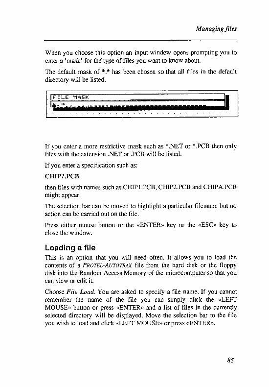
Managing files
When you choose this option an input window opens prompting you toenter a 'mask' for the type of files you want to know about.
The default mask of *.* has been chosen so that all files in the defaultdirectory will be listed.
F I LE 1 , IA5Krfr
If you enter a more restrictive mask such as *.NET or *.PCB then onlyfiles with the extension .NET or .PCB will be listed.
If you enter a specification such as:
CHIP?.PCB
then files with names such as CHIPI.PCB, CHIP2.PCB and CHIPA.PCBmight appear.
The selection bar can be moved to highlight a particular filename but noaction can be carried out on the file.
Press either mouse button or the <ENTER> key or the <ESC>> key toclose the window.
Loading a f i leThis is an option that you will need often. It allows you to load thecontents of a Pnoret-Aurornur file from the hard disk or the floppydisk into the Random Access Memory of the microcomputer so that youcan view or edit it.
Choose File Load. You are asked to specify a file name. If you cannotremember the name of the file you can simply click the <LEFTMOUSE>> button or press <ENIER>> and a list of files in the currentlyselected directory will be displayed. Move the selection bar to the fileyou wish to load and click <LEFT MOUSE>> or press <ENTER>>.
85
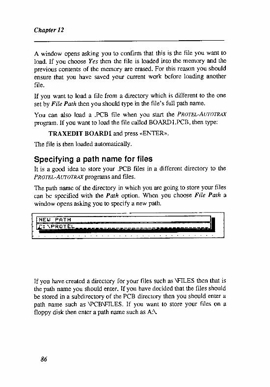
Chapter 12
A window opens asking you to confirm that this is the file you want to
load. If you choose Yes then the file is loaded into the memory and the
previous contents of the memory are erased. For this reason you should
ensure that you have saved your current work before loading another
file.
If you want to load a file from a directory which is different to the one
set by File Path then you should type in the file's full path name.
You can also load a .PCB file when you start the Pn }TEL-AUT}TRN(program. If you want to load the file called BOARDl.PCB, then type:
TRAXEDIT BOARD1 and press (<ENfER>>.
The file is then loaded automatically.
Specifying a path name for fi lesIt is a good idea to store your .PCB files in a different directory to the
P nornt-Atnornex program s and files.
The path name of the directory in which you are going to store your files
can be specified with the Path option. When you choose File Path a
window opens asking you to specify a new path.
I t IEU PATH
: \ P R O T E L
If you have created a directory for your files such as VILES then that is
the path name you should enter. If you have decided that the files should
be stored in a subdirectory of the PCB directory then you should enter apath name such as \PCBVILES. If you want to strore your files on afloppy disk then enter a path name such as A\
86
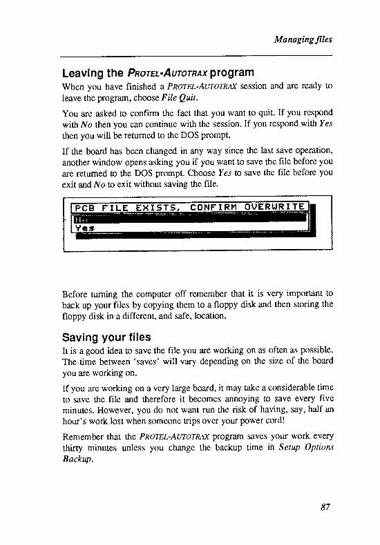
Managing ftles
Leaving the Pnorer-AltrorRAx programWhen you have finished a Pnorrt-AvtornAx session and are ready to
leave the progritm, choose File Quit.
You are asked to confirm the fact that you want to quit. If you respond
wittr No then you can continue with the session. If you respond with Yes
then you will be returned to the DOS prompt.
If the board has been changed in any way since the last save operation,
another window opens asking you if you want to save the file before you
are returned to the DOS prompt. Choose Yes to save the file before you
exit and No tn exit without saving the file.
Before turning the computer off remember that it is very important to
back up your files by copying them to a floppy disk and then storing the
floppy disk in a different, and safe, location.
Saving your f i lesIt is a good idea to save the file you are working on as often as possible.
The time between 'saves' will vary depending on the size of the board
you are working on.
If you are working on a very large board, it may take a considerable time
to save the file and therefore it becomes annoying to save every five
minutes. However, you do not want run the risk of having, sY, half an
hour's work lost when someone trips over your power cord!
Remember that ttre Pn ornr-AwoTR*( program saves your work every
thiny minutes unless you change the backup time in Setup OptionsBackup.
87
Chapter 12
When you do decide to save, you will be asked to supply a file name, orelse a file name will be specified in the input window. If you want togive the file a new name simply type in the narne. If you want to give itthe same name as a file which is already stored on the disk then you willbe asked to confirm the fact that you want to overwrite the file. chooseYes then click (LEFT MOUSE>> or press <ENTER>>.
Once the file has been saved then you can continue working.
You should also be aware that when you save a file, a backup of theprevious version of the file with the extension .BAK is created. For ttrisreason you must ensure tlrat there is always nvice the disk spaceavailable than that needed just for the .PCB file.
88

13 sErnNG GRID stzEs
There are two grids which are active in the PnorEbAurorR$( program.
The first is an invisible 'snap' grid and the second is a visible gnd guide
which takes the form of an alrray of dots on the screen.
The distance between points in either gnd can be varied by choosing the
Grid option from the MAIN MEN[.J.
ffi I D 5s
f f i i b t e 6 r i d : l E q q
Changing the snap gr idThe'snap' grid is an invisible grid which the cursor follows (or snaps to)
whenever the cursor keys or the mouse move the cursor around the
screen. As the cursor moves it 'snaps' from one gnd position to the next.
Move to the point where you will start connecting the pads, choow Grid
Snap then change the value to, say, 125. Now each time you move the
mouse or press the cursor keys the cursor will snap to the next pad
position"
The normal value is 25 rnils but this value can be increased or decreased
depending on your preference. The current value of the snap gid is
always shown on the status line at the bottom of the screen.
One example of where this is useful is when you want t{l work with edge
connecror pads which are usually either 125 or 156 mils apart. An
example might be if you were going to connect some of the pads of, say,
89

Chapter 13
a STEDGE or S 100 connector to the ground or power planes.
When a grid size is selected, the gnd points originate at X:0 Y:0regardless of whether there is a floating origin. Thus if the cursor is atX:100 Y:100 and you change the snap grid to 30, the cursor wouldimmediately snap to X:90 Y:90 as that is the nearest grid point.
Changing the visible gridThe visible grid helps you to lay components and tracks in a careful andsystematic way.
It is usually set to 1000 mils (i.e. one inch) but the value you will need towork with varies greatly depending on the level of magnification youchoose. The higher the magnification the lower the value of the visiblegrid you need.
To change the value, select Grid Visible Grid and enter the new value.Press <ENIER>> or click <LEFT MOUSE>> to exit from the option.
90

1 4 HlcHLtcHrtNG NETs
The Hightight option lets you carry out two main functions. First you
can highlight a net or a single connection or copy a net and second you
can create a netlist based on the existing set of connections.
The highlight option is used widely to verify nets. It helps you make sure
that all the connections that need to be made, have been made.
r-I 6I.IL I BHT
D u p l i c e t sItf etl ' f sker Net L iFt -
Highl ight ing a connect ionChoose Hightight Connection to highlight a connection between two
pads. The prompt:
SELECT TRACK/PAD TO HIGHLIGTII
appears on the prompt line. Move the cursor to a track or pad in the
r-onn*tion you want t,o highlight, then press (<ENTER>> or click <LEFT
MouSE>>. The message 'SORTING TRACKS. PLEASE WAIT.'
appears at the top of the screen, then the connection is highlighrcd.
The highlight remains until you either highlight another connection or
net or until you selecr Hightight Connection or Highlight l'{et and
9I
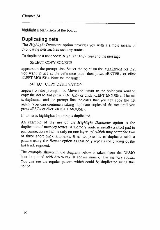
C hapter 14
highlight a blank area of the board.
Duplicat ing nets'fhe Highlight Duplicate option provides you with a simple means ofduplicating nets such as memory routes.
To duplicate a net choose Highlight Duplicate and the message:
SELECT COPY SOURCE
appears on the prompt line. Select the point on the highlighted net thatyou want trr act as the reference point then press <ENTER> or click<LEFT MOUSE>). Now the message:
SELECT COPY DESTINATION
appears on the prompt line. Move the cursor to the point you want tocopy the net to and press <ENTER>> or click <LEFT MOUSE>). The netis duplicated and the prompt line indicates that you can copy the netagain. You can continue making duplicate copies of the net until youpress <ESC> or click <RIGHT MOUSE>).
If no net is highlighted nothing is duplicared.
An example of the use of the Highlight Duplicate option is theduplication of memory routes. A memory route is usually a short pad topad connection which is only on one layer and which may comprise twoor three short track segments. It is not possible to duplicate such apattern using the Repeat option as that only repeats the placing of thelast track segment.
The example shown in the diagram below is taken from the DEMOboard supplied with Atnornex. It shows some of the memory routes.You can see the regular pattern which could be duplicated using thisoption.
92
Highlighting nets
Highl ight ing a netThe Highlight Ner option is similar to the Highlight Connection option.The only difference is that the Highlight N et option highlights acomplete net, whereas Highlight Connection only highlights oneconnection.
Creating a netl istIf you have routed a board and want to create a netlist, use the HighlightMake Netlist option.
One reason why you might want to produce a netlist after you have madeall the connections is to obtain a printed copy of the netlist for manualchecking of connections. Another reason might be that you do not havethe Pn org,t-ScHEMATIC pro,gram which produces netlists and have had tomake all connections using the pad to pad router. You might want tocreate a netlist and submit the netlist to the automatic router to produce abetter result,
When you choose Highlight Make Netlist, 3D input window with theheading 'NETIIST FILENAME' opens. At this stage you should enterthe name for the netlist file which is to be created.
You are now asked tro confirm that you want the netlist generation toproceed. Choose Yes and the nets are highlighted one by one as they are
93

Chapter 14
stored in the file. You will notice that on the right hand side of the statusline a recursion depth count is provided. This simply indicates howhard the program is 'thinking' in working out the nets!
The netlist generation continues until all nets have been stored in the file.At this stage the status line is restored and the cursor reappears on the
board.
The file that is saved has the extension .NET.
94
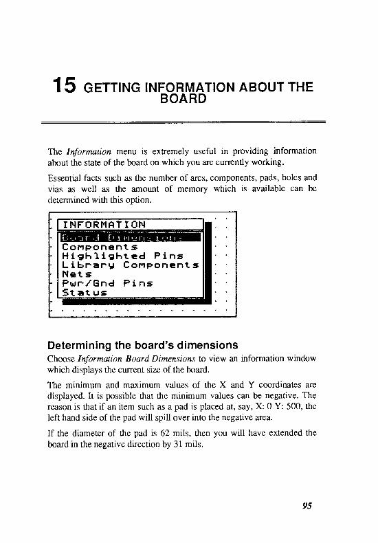
15 GETTING INFORMATION ABOUT THEBOARD
The Information menu is extremely useful in providing information
about the state of the board on which you are currently working.
Essential facts such as the number of arcs, components, pads, holes andvias as well as the amount of memory which is available can bedetermined with this option.
I I {FORI ' IAT I ON
C o t u t p o n € n t sH t s h l i s h t e d P i n sL i b n e r ' U C o n ' t p o n e n t sN c t sP t ^ l r l G n d P i n s5 t e t u g
Determining the board's dimensionsChoose Information Board Dimensions to view an information windowwhich displays the current size of the board.
The minimum and mzurimum values of the X and Y coordinates aredisplayed. It is possible that the minimum values can be negative. Thereason is that if an item such as a pad is placed at, sy, X: 0 Y: 500, theleft hand side of the pad will spill over into the negative area.
If the diameter of the pad is 62 mils, then you will have extended theboard in the negative direction by 3l mils.
9s
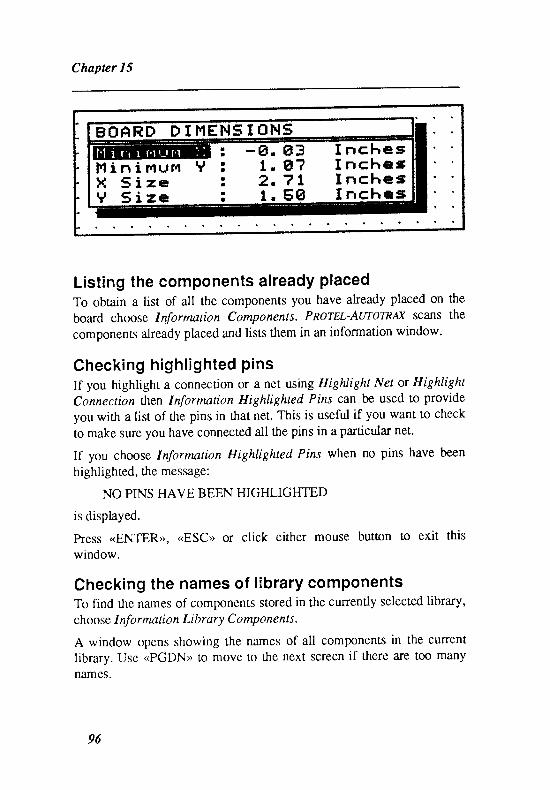
Chapter 15
EmARp D Il'f EHs I o_DI-_s: -E f .: t ,: 2 .: 1 .
F f i n i H U n 4 Ylt 5 i zeY S i z e
6 3a ?7 16 E
I n c h e sI n c h e sI n c h e gI n t r h e s
I t
t t
a a
I t
a a
t a
Listing the components already placedTo obtain a list of all the components you have already placed on the
board choose Information Components. Pnorr,t-Atnornur scans the
components already placed and lists them in an information window.
Checking h igh l ighted PinsIf you highlight a connecrion or a net using Highlight Net or Highlight
Connection then Information Highlighted Pins can be used to provide
you with a list of the pins in that net. This is useful if you want to check
to make sure you have connected all the pins in a particular net.
If you choose Information Highlighted Pins when no pins have been
highlighted, the message:
NO PINS HAVE BEEN HIGHLIGHTED
is displayed.
Press <ENTER>), <ESC> or click either mouse button to exit this
window.
Checking the names of l rbrary componentsTo find the names of components stored in the currently selected library,
choose Information l-ibrary Components.
A window opens showing the names of all components in the current
library. Use <PGDN>) [o move to the next, screen if there are too many
names.
96

Getting information about the board
press <ENTER>>, <ESC> or click either mouse button to exit this
window.
Listing all the netsThis option allows you to obtain a lisf of all nets which are culrently in
the mernory. Choose Information Nets and a window listing the nets
opens. Remember that if there is more than one window-full, press
<PGDN>> to see more.
press <ENTER>>, <<ESC>> or click either mouse button to exit this
window.
If no nets have been loaded with the Ne tlist Get Nets option then the
message:
NO NETS LOADED
is displayed.
Listing power and ground plane netsTo obtain a list of all the power nets or ground nets, choose Information
PwrlGnd Pins. A menu appears which allows you to choose the ground
plane or ttre power plane.
Choos e Ground Plane tn list all connections to the ground plane. Choose
Power Plane to list all connections to the power plane.
Press <ENTER>), <ESC> or click either mouse button to exit this
window.
Essential intormation about the boardThis option allows you to check information about the board. Choose
Infornation Status. An information window opns which shows the
following details.
97
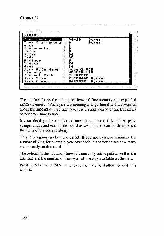
Chapter 15
5 T A T U 5
F r e c E n s l Y { e n o F uA r c sC o m p o n e n t g sF i I l sH o l e gPadgs5 t r i r g sT n a c k sU i a gU o n k F i l r N a m rL i b r a r uC u n r e n t P a t hD i s k 5 i z eD i s k F r e e
3 9 4 2 9aI6g6 65 gB7 41 6n o g e r Z . P C B1 . { E U L I B . L I BC : \ F R O T E L2 1 3 A 9 4 4 F � B s t e s9E �99328 Bu t es
B u t e sB u t e s
The display shows the number of bytes of free memory and expanded(EMS) memory. When you are creating a large board and are worriedabout the amount of free memory, it is a good idea to check this statusscreen from time to time.
It also displays the number of arcs, components, fills, holes, pads,strings, tracks and vias on the board as well as the board's filename andthe name of the current library.
This information can be quite useful. If you are trying to minimrze thenumber of vias, for example, you can check this screen to see how manyare curTently on the board.
The bottom of this window shows ttre cunently active path as well as thedisk size and the number of free bytes of memory available on the disk.
Press <<ENTER>>, <ESC> or click either mouse button to exit thiswindow.
98
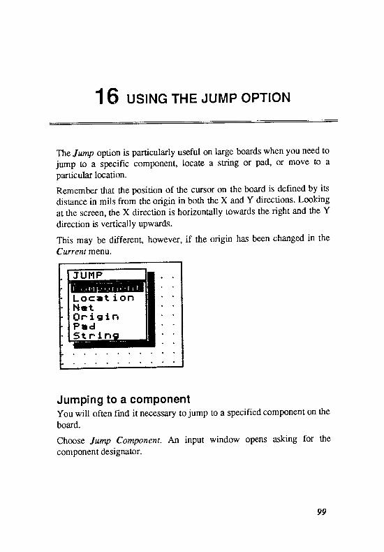
16 ustNc rHE JUMP oPTloN
The Jump option is particularly useful on large boards when you need to
jurnp to a specific compcnent, locale a string or pad, or move to a
particular location.
Remember that the position of the cursor on the board is defined by its
distance in mils from the origin in both the X and Y directions. Looking
at the screen, the X direction is horizontally towards the right and the Y
direction is vertically upwards.
This may be different, however, if the origin has been changed in the
Current menu.
JUl , IP
L o c a t i o nN c tO r i e i nP e dS t r l n
a a
Jumping to a componentYou will often find it necessary to jump to a specified component on the
board.
Choose Jump Cornponent. An input window opens asking for the
component designator.
99
Chapter I6
If you can't remember the designator, simply click <LEFT MOUSE>> orpress <ENTER> and an information window opens showing allcomponent designators on the board.
Move the selection bar to the designator required and click <LEFTMOUSE> or press <ENTER>>. The cursor jumps to pin I of thecomponent, you requested.
Try this with the DEMO.PCB file loaded. Choose Jump Component,then input U5 which is the designator for the 280 microprocessor. Noticethat the cursor jumps to the square pad which specifies pin I on the chip.
Jumping to a locationThis option allows you to specify a location on the board for the cursorto jump to. Choose Jump Location. A window opens asking you to inputthe X location. The value in ttre window shows the current position ofthe cursor. Type in the new value. A window now opens asking for the Ylocation. Type in the Y value and press (ENTER> or click <LEFTMOUSE>>.
The cursor immediately relocates at the new coordinate.
It may appear to be srange that the default value given in the inputwindow is the current cursor position. If you are already at that positionwhy would you want to jump there? The reason is that in specifying acoordinate to jump to, you may make a mistake in typing the numbers. Ifyou do then you can easily edit the incorrect number rather than typingboth coordinates in again.
Jumping to a netThis option allows you to position the cursor on a particular net.
Choose Jump lt{et. An input window opens asking you to enter the nameof the net. If you cannot remember the name enter a (<?>) and aninformation window listing all ttre net names opens. You can ttren selectthe appropriate net name by moving the selection bar to the name andpressing <ENTER>> or clicking <LEFT MOUSE>>.
If the net exists then the cursor jumps to the nearest pad in that net.
100
Using the Jump option
If the net does not exist or if no nets are loaded then the message:
NETNAMENOTFOUND
or the message:
NO NETS LOADED
is displayed.
Wirh the DEMO.PCB rile and the DEMO.NET file loaded try jumpingto ttre net CPUCLK and the net GND.
Jumping to the or ig inThis option simply relocates the cursor at the absolute origin in the
bottom left hand corner of the board, regardless of whether a floating
origin has been set.
Choose Jump Origin and ttre cursor is immediately relocated.
Jumping to a padThis option allows you to specify a component to jump to. Choose JumpPad. Select the component by jumping to the component or by moving
to it with the mouse or the ilrow keys. Press <ENTER>> or click <LEIT
MOUSE>).
An input window then opens asking you to enter a pin number. Type in apin number and the cursor jumps to that pad.
This is useful when connecting pads if you need to remember the orderin which the pins are numbered. This is not usually a problem with ICs,but it is possible to forget the numbering system for connectors such asDB25s.
If the pin number that you specify does not exist (e.g. if you input pin 17for a DIP16 pattern) then the message:
PAD NOTFOLTND
is displayed.
IOI
Chapter 16
Jumping to a str ingThis option allows you to jump to a string that you specify. Choose
Jump String. An input window opens asking you !o enter the string tojump to.
If there is more than one marching string on the board Pnornt-Awornurwill do an exact match first. Therefore if you type in Pro, it will firstlyfind the string Pro, then PRO then pro then any other beginning withPro... and so on.
If you attempt to jump to a string which does not exist, the message:
STRING NOTFOLIND
is displayed.
r02

17 MANAGING LIBRARIES
The Library menu provides the options you need to create new library
components, manage existing libraries of components and create new
libraries.
L r eRABt
B r o w r oC o m P a c tD c l c t eE x p l o d eF i l eL i s tlv,l e n grN e w L i b r ' a F UR e n a n l c
Adding components to the l ibraryBefore you can add a component to the library you must first create it
with the normal tools available ttrrough the Pnorg,t-Atnornur program.
Most components can be created with tracks, arcs and pads. The
procedure for doing this is described in detail in Ch aptst 4.
When you have created the component, mark it as a block using the
Block Define option.
Then choose Library Add. Enter a name for the new component. The
message:
CREATING LIBRARY COMPONENT
is displayed briefly as the component is added to the currently selected
library.
Browsing through l ibrary componentsThe Library Browse option allows you to inspect the patterns of
103
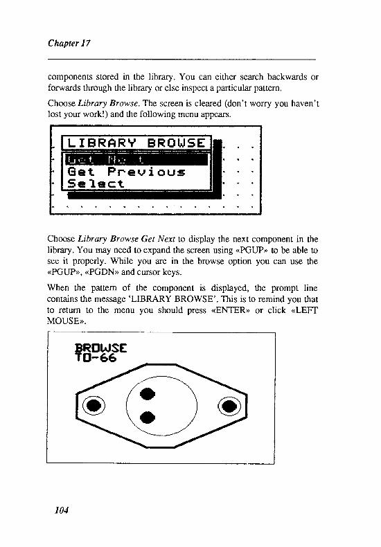
Chapter 17
components stored in the library. You can either search backwards orforwards through ttre library or else inspect a particular pattern.
Choose Library Browse. The screen is cleared (don't worry you haven'tlost your work!) and the following menu appears.
L I B R A R Y B R O U S E
E e t P r e u i o u s5 e L e c t
Choose Library Browse Get Next to display the next component in thelibrary. You may need to expand the screen using <PGUB) to be able tosee it properly. While you are in the browse option you can use the<PGIJPr>, ..PGDN> and cursor keys.
When the pattern of the component is displayed, the prompt linecontains the message 'LIBRARY BROWSE'. This is to remind you thatto return to the menu you should press (ENIER> or click <LEFTMOUSE>>.
ERIIT^JSETB-66
JO
104
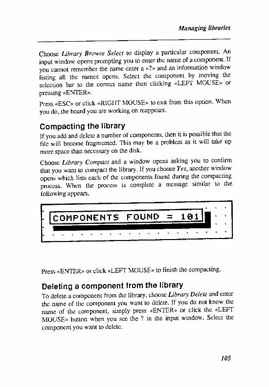
Managing libraries
Choose Library Browse Select to display a particular component. An
input window opens prompting you to enter the name of a component. If
you cannot remember the name enter a <<?>> and an information window
iisting all the names opens. Select the component by moving the
selection bar to the correct name then clicking <LEFT MOUSE> or
pressing <ENTER>>.
press <<ESC>> or click <RIGHT MOUSE>> to exit from this option. When
you do, the board you are working on reappears.
Compacting the librarYIf you add and delete a number of components, then it is possible that the
file will become fragmented. This may be a problem as it will take up
more space than necessary on the disk-
Choos e Library Compacr and a window opens asking you to confirm
that you want to compact the library. If you choose Yes, anottrer window
opens which lists each of the components found during the compacting
pi*.5. When the process is complete a message similar to the
following appears.
press <ENTER>> or click <LEFT MOUSE>> to finish the compacting.
Deleting a component from the IibraryTo delete a component, from the library, choose Library Delete and enter
the name of the component you want to delete. If you do not know the
name of the component, simply press <ENTER> or click the <LEFT
MOUSE> button when you see the ? in the input window. Select the
component you want to delete.
105

Chapter 17
You are asked to confirm the fact that you want to delete the component.Choose Y es to delete it.
'Exploding' a componentOften, when you want to design a new component there is already acomponent in the library which is similar and may only need minormodifications. If that is the case you can place the existing librarycomponent on the board and explode it. Having 'exploded' thecomponenL you can edit it and then save ttre edited version as a newlibrary component.
Choose Library Explode and you are asked to select the component youwant to 'explode'. Move to the component and press <ENTER>> or click(<L,EFT MOUSE>>.
The component will appear to be basically unaltered (except for thedesignator and comment which will be removed) but each element of thecomponent will now be in its primitive state. That is, instead of a singlecomponent, it is now a collection of tracks, arcs, and pads.
To convince yourself of this, move to any other component and selectthe top overlay (bV pressing <<+>) or (<->> on the keypad). Now choose EditTrack and move the cursor over the track portion of a component. Youwill not be allowed to edit the track! Try the same thing with acomponent which you have exploded - you can now change the track.
Once you have changed the pattern you must then define it as a blockand add it to the library as a new component as described in the tutorialin Chapter 4.
This option is also useful if you want to make minor adjustments toexisting library patterns.
Choosing a dif ferent l ibrary f i leChoose the Library File option to change the currently selected libraryfile. A different directory or disk drive can be specified if required.
A window opens with the prompt 'LIBRARY FILE NAME'.
Enter the name of the library file you want to make active. If you cannotremember the name, enter a <<?r, and a list of the .LIB files is displayed.
r06
Managing libraries
Move the selection bar to the one you want to open then press (ENTER>>
or click <LEFT MOUSE>).
Remember that you can check the name of the currently active library by
choosi ng I nformntion S tatus.
Listing the l ibrary componentsChoos e Library List to list the names of components in the currently
selected library. The message 'WORKING. PLEASE WAIT.' is
displayed at the top of the screen and then an information window will
open displaying the names of the components in the library.
If you need to check the names of components in other libraries you
must first change the currently selected library with Library Files as
described above.
Merging I ibrariesThis optiOn allows you to move a component from another library into
the existing library.
ChooseLibrary Merge.You are asked to enter the name of ttre library to
merge from. Enter the name of the library from which you want to
move the component. You are then asked to enter ttre name of the
component you want to merge. If the component exists then it will be
added o the curently selected library.
Creating a new librarYThis option allows you to create a new library. Choose Library New
Library. You are promptsd to supply the name for the new library. A
new library file is created on the disk with the extension .LIB.
If you g'y tg specify a name for the new library which is the same as a
library which already exists, then the message:
LIBRARY FILE ALREADY EXISTS
will be displayed.
It removes the existing library from the memory Out not from the disk)
and allows you to create a library with a new set of components. You
107

Chapter 17
can, of course, use Library Merge to move components from otherlibraries into the new library.
Renaming a componentThis option allows you trr rename a component. Choose LibraryRename. You are asked to rename a component in the crrrently selectedlibrary. The message:
NAIVIE INLIBRARY
appears.
Enter the name of the component whose name you want to change. Themessage:
NEW LIBRARY COMPONENT NAME
then appears. Enter the new name for the componenl
If the component does not exist, the message:
COMPONENT NOT FOUND IN LIBRARY
is displayed.
r08
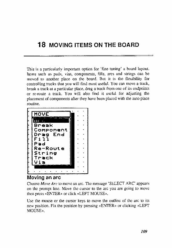
18 MovtNG trEMs oN THE BoARD
This is a particularly important option for 'fine tuning' a board layout.
Items such as pads, vias, components, fills, arcs and strings can bemoved to another place on the board. But it is the flexibility for
controlling tracks that you will find most useful. You can move a track,break a track at aparticular place, drag a track from one of its endpointsor re-route a track. You will also find it useful for adjusting theplacement of components after they have been placed with the auto place
routine.
1'louE
B n e e kC o n ' t p o n e n tD r e g E n dF i 1 1P a dR e - R o u t eS t r i n gT r a c kU i a
t t
l !
t l
t a
l a
t t
! a
a l
Moving an arcChoose Move Arc to move an arc. The message 'SELECT ARC' appearson the prompt line. Move the cursor to the arc you are going to movethen press <ENIER>> or click <LEFT MOUSE>>.
Use the mouse or the cursor keys to move the outline of the arc to itsnew position. Fix the position by pressing <ENTER>> or clicking <LEFTMOUSE>>.
r09
Chapter 18
You are now prompted to select another arc. If you have finished
moving arcs, press <ESC> or click <RIGHT MOUSE>>. Otherwise you
can select another arc and move it in the same way.
Breaking a trackSometimes you may want to make a Eack shorter or break a track into
two sections. To do this choose Move Break. The prompt 'SELECT
TRACK' appears. Move the cursor to the exact spot on the track where
you want to break it.
The track now acts like a 'rubber band'. If you move the cursor, the track
stretches in two sections as if it were a rubber band held at the cursorposition. The message:
DRAGGING BROKENTRACK
is displayed on the prompt line.
When you have placed the tracks, press <ENTER> or click <<LEFT
MOUSE>>.
The important thing to note about this option is that it 'breaks' the track
into two Eacks. Each part will now be recognised as a nack so one
section can be deleted if required. This is a simple way of making a track
shorter.
Moving a componentChoose Move Component to move a component to a new position on the
board"
The message 'SELECT COMPONENT' on the prompt line indicates
that you should move the cursor to the component that you want tomove. Press <ENTER> or click <LEFT MOUSE> ttl select the
component.
The message on the prompt line will be replaced with 'MOVING
COMPONENT'. As you move the cursor, an outline of the component
also moves.
Place the component in is new position by moving it with the mouse orthe cursor keys. Refer to page ffi for details of how to rotate thecomponenl
I IO

Moving items on the board
A window opens asking if you want to 'DRAG TRACKS'.
If you tlren want the tracks to retain their'connectivity'then select Yes.
At this stage all tracks are stretched to reach the new position of the
component. Don't worry about the fact that the tracks are distorted. You
can re-route them later. If you choose No, the component is moved but
the tracks will remain in position, thus breaking any connections.
A powerful feature of tlre Move Component option is that it can be used
to 'fine tune' the placement of components prior to routing. To
understand the process, work through the following example.
Choose File Load and load the unrouted PCB called PLACED. Now
choose lti.etlist Get Nets and load the netlist called DEMO. Now choose
Netlist Show All Nets. You will now see the 'ratsnest' of connections
displayed.
Now choose Move Component and select the component, with the
designator U7. Move the component and notice how the ratsnest moves
with the component. Using this technique you can move critical
components to other places on the board to try to reduce track
congestion.
1il"Itt
' s - ( +'tN.t l--
rb)\Y-t
f
i . /
I
--:_-:.-- f---r#+-
- -t
:-: -:F;i{T
t I t
Chapter 18
Dragging the end of a trackThis option allows you to drag the end of a track to another place on the
board while maintaining its connection to other Eacks.
Choose Move Drag Track and you are prompted to select a ftack. Move
to the track you want to drag and click <LEFT MOUSE> or press
<ENTER>). The cursor jumps to the closest track end and the message:
DRAGGING TRACKEND
appears on the prompt line. You can now drag ttre track to the new
position. Any connected Eack will also be dragged and vias will be
repositioned.
Note that the track you select must be on ttre currently selected layer.
Moving a f i l lChoose Move Fill to move a fill. The message 'SELECT FILL' appears
on the prompt line. Move the cursor to the till you are going to move
then press <ENTER>> or click <LEFT MOUSE>>.
The message 'MOVING FILL' on the prompt line indicates that you
should use the mouse or the cursor keys to move the outline of the fill to
its new position. Fix the position by pressing <ENIER> or clicking<LEFT MOUSE>>.
You will now be prompted to select another fill. If you have finished
moving them, press <<ESC> or click (RIGHT MOUSE>).
Moving a padChoose Move Pad if you want to move a pad. The message 'SELECT
PAD' appears on the prompt line. Move the cunor to the pad you aregoing to move then press <ENTER>> or click <LEFT MOUSE>>.
Use the mouse or the cursor keys to move the outline of the pad to its
new position. Fix the position by pressing <ENITER>> or clicking <LEFT
MOUSE>>.
You are now prompted !o select another pad. If you have finished
moving pads, press (ESC> or click <RIGHT MOUSE>>. Otherwise you
can select another pad and move it in the same way.
I12
Moving items on the board
Re-routing a trackThe Move Re-Route option allows you to manually route a connection
by breaking the track at a number of points. The sections remain
anchored to the pads or vias at either end.
You break the tracks and choose the new route in the same way as that
described in the Move Break section above.
Moving a stringChoose Move String if you want to move a string. The message'SELECT STRING' appears on the prompt line. Move the cursor to the
string you are going to move then press <<ENTER>> or click <LEFT
MOUSE>). Note that you can position the cursor anywhere on the string.
Use the mouse or the cursor keys to move the outline of the string to its
new position. Refer to page 66 for details of how to rotate the string. Fix
the position by pressing <ENIER>> or clicking <LEFT MOUSE>>.
You are now prompted to select another string. If you have finished
moving strings, press <ESC> or click <RIGHT MOUSE>>. Otherwise you
can select another string and move it in the same way.
Moving a trackWhen you want to move a track, choose MoveTract and then move the
cursor to the track you are going to move. Remember that a track is a
single line segment, not the entire connection between two pads.
Select the track you want to move by pressing <<ENTER>> or clicking(LEFT MOUSE>). The message 'MOVING TRACK' appears on the
prompt line. At this stage you can move the track to the required
position.
When you move the track, connectivity with vias and related tracks is
maintained, so connected tracks and vias are dragged with the Eack.
Pads are not moved with the track, however.
1 1 3
Chapter 18
Moving a viaChoose Move Via if you want to move a via. The message 'SELECT
VIA' appears on the prompt line. Move ttre cursor to the via you aregoing to move then press <<ENIER>> or click <LEFT MOUSE>>.
Use the mouse or the cursor keys to move the outline of the via to itsnew position. Fix the position by pressing <ENTER>> or clicking <LEFTMOUSE>>.
You are now prompted to select another via. If you have finishedmoving vias, press <ESC>> or click <RIGHT MOUSE>>. Otherwise youcan select another via and move it in the same way.
Note that the tracks which are connected to the via are stretched tomaintain their connectivity.
I14
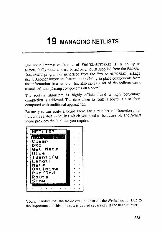
19 MANAGING NETLISTS
The most impressive feature of Pnors,r-Aurornetr is its ability to
automatically route a board based on a netlist supplied from the PnoTEL-
Scnnuerrc program or generated from the Pn ornt-AurorR${ package
itself. Another important feature is the ability to place components from
the information in a netlisl This also saves a lot of the tedious work
associated with placing components on a board.
The routing algorithm is highly efficient and a high percentage
completion is achieved. The time taken to route a board is also short
compared with traditional approaches.
Before you can route a board there are a number of 'housekeeping'
functions related to netlists which you need to be aware of. The N etlist
menu provides the facilities you require.
H E T L I 5 T
C l c a r *DRtrB e t H c t sH i d eI d e n t i f uL e n g t hIr let sO p t l n i z eP r r r / 6 n dR o u t oSho t i f
! r
! a
you will notice that the Route option is part of the t{etlist menu. Due to
the importance of this option it is reated separately in the next chapter.
1 1 5

Chapter 19
Placing components automaticallyOnce you have generated a netlist with the Pn ornt-ScHEMATIC package,you can have the components placed automatically by choosing theNetlist Auto Place option.
This option has been designed to reduce the tedium involved in placingmany components on a board. It does not necessarily produce the bestplacement and some 'tidying' work inevitably needs to be done. As arough estimate it may reduce the time you spend placing components byup to 90Vo.
Before you begin it is a good idea to follow two simple rules. The first isto manually place any edge connectors or other components which mustbe in a particular place on the board. Placing them manuallyautomatically marks the component as '[,ocked in Place'. The secondrule is to place any 'seed' components which you want to build the boardaround. An example of a seed component might be a microprocessorchip.
The board will be 'built' out from the corners of the board, from thecorners of keep ouf areas and from the corners of pre-placed
components.
Be aware that with very small boards some strange things may happen.Nevertheless it is still quicker to use the A uto Place routine then movethe components manually.
If the message:
NO OUTLINE ON TI{E KEEPOUTLAYER
is displayed this means that you have not defined the border withinwhich the components are to be placed. To overcome this, turn theKeepout layer 'on' with Setup Toggle Layers, then select that layer bypressing the <<+>> key on the numeric keypad.
Draw an outline using Place Tracfr which defines the limits of the board.Now hide ttre Keepout layer again and retun to the Auto Place routine.
I I6

Managing netlists
Clearing a netl istIf you want to load a netlist you sometimes need to clear an existingnetlist from the memory. Also when you have finished routing, you maywant to clear the netlist to reduce the amount of memory used.
Choose Netlist Clear. You are asked to confirm that you want to clearthe nets from the memory. ChooseYes to confirm the action.
If you choose this option when there is no netlist in the memory themessage:
NO NETS LOADED
is displayed.
Checking the design rulesThe Netlist DRC option allows you to check to see that the tracks, viasand pads have been placed according to a set of rules which you havenominated. The process is known as design rule checking.
The process is particularly important after you have laid some tracksmanually.
The DRC option first loads the netlist file, then checks to see ttrat allnodes in each net are connected. If they are not, an error is generated andthe net is broken into sub-nets. At this stage it also checks to see if thereare any extra pins.
In the next step all nodes are highlighted and a check is made to see ifanything which is not highlighted is closer than the design rule checkallows.
Loading a netl istOne simple way of creating a netlist that contains the informationPnorr,r-Atnornur requires to lay all the necessary tracks is to use thePnornt-Scng,ueTlc package. You can also generate a netlist using theMake Netlist option in the Highlight menu.
In each case the netlist is stored on the disk in a file with a .NETextension.
117
Chapter 19
To load a netlist choose lr{etlist Get Nets. An input window opensprompting you to enter the filename of the netlist you want to load. Thewindow displays the default value *.NET.
If you cannot remember the filename simply press <ENTER> or clickthe <LEFT MOUSE>> buffon.
A window opens displaying the names of ttre files with a .NETextension. Move the selection bar to the file you want to load and click<LEFT MOUSE>> or press (ENTER>>.
Each net is now loaded and the names are displayed in a window at thetop of the screen. You are then asked to select the optimization methodyou want to use. Select one of the mettrods and ttre nets are optimi zeA toreduce the overall length of each net. You are then returned to the Ne tlistmenu.
If you try to load a netlist when there is already one in the memory, themessage:
NETLIST ALREADY LOADED, CONFIRM LOAD
will be displayed. Choose Yes if you want to load the new netlist andoverwrite the one in the memory.
Hiding netsIf you have already displayed a set of nets (perhaps through the Showoption) you can hide some or all of them with the Ne tlist Hide option.The following window appears.
H I D E H E T
N e t s O n C o m p o n r n tA 1 1 l t f e t s
Choose Select Nets to specify the names of some of the nets, or chooseAII Netr to hide all the nets which are currently displayed.
tr8

Managing netlists
ldentifying netsOnce you have loaded a netlist, you can identify any net with the Ne tlist
Identify option. Firstly, you need to chooseNetlist Show All Nets so thatyou can see the 'ratsnest' of connections.
When you choose ldentify you are prompted to select a connection.
Move the cursor to the net you want to identify then press <ENTER>> or
click the <LEFT MOUSE> button.
A window now appears displaying the net name of the connectionpointed to by the cursor. Press <<ESC> or click <RIGHT MOUSE>> to exitfrom this option.
Determining the connection lengthIf you ile concerned about the total length of the connections and,perhaps, want to optimize ttre [hem, then you can determine ttre totallengtlr by choosing Netlist Length. A window opens showing the total
connection length in inches.
T O T N U C O N H E C T I O N L E N B T H1 8 . 4 2 3 I n c h e E
a t
i !
t t
l a
Listing net namesChoose Netlist Ners to obtain a list of the names of all nets currentlyloaded. Remember that you can use the <<PGUP>) and (<PGDN> keys toscroll through the names if there are more than will fit in one window.
Optimizing netsNets are automatically optimized when they are loaded from the disk.Each net is checked to determine the shortest path benveen the variousnodes. If you have changed a number of nets you may need to optimizeagain before you route the board.
119
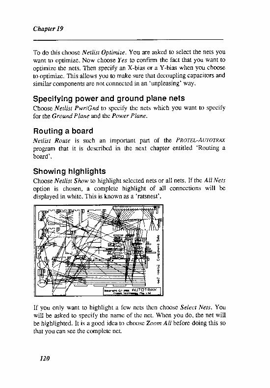
Chapter 19
To do this choose Netlist Optimize.You are asked to select the nets you
want tro optimrze. Now choose Yes to confirm the fact that you want to
optimi ze the nets. Then specify an X-bias or a Y-bias when you choose
to opti mize. This allows you to make sure that decoupling capacitors and
similar components are not connected in an 'unpleasing' way.
Specifying power and ground plane netsChoose Netlist PwrlGnd to specify the nets which you want to specifyfor the Ground Plane and the Power Plane.
Routing a boardNetlist Route is such an important pan of the Pnors,t-Atnornurprogram that it is described in the next chapter entitled 'Routing aboard'.
Showing highl ightsChoose Netlist Show to highlight selected nets or all nets. If the AII Nets
option is chosen, a complete highlight of all connections will be
displayed in white. This is known as a 'ratsnest'.
If you only want to highlight a few nets then choose Select Nets. Youwill be asked to specify the name of the net. When you do, the net willbe highlighted. It is a good idea to choo se Zoom A// before doing this sothat you can see the complete net.
120
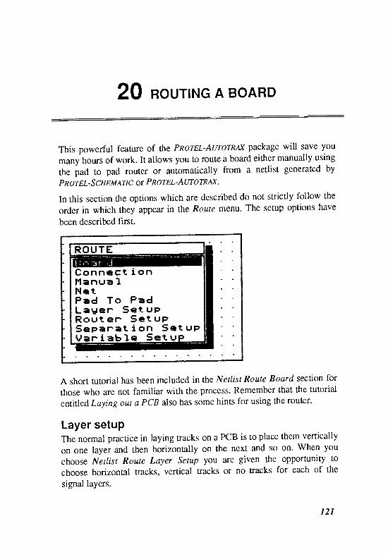
Zg RourlNG A BoARD
This powerful feature of the Pn ornuAurorR$( package will save you
manyhogrs of work. It allows you to route a board either manually using
the pad to pad router or automatically from a netlist generated by
P n orgr- S c n tu eTI c or P nor nt-ALrrorRu{ .
In this section t6e options which are described do not strictly follow the
order in which they appear in the Route menu. The setup options have
been described first.
R O U T E
C o n n e c t i o nl ' l anua IN e tP a d T o P a dL a U € r S e t u PR o u t e r S e t u PS e p e n e t i o n S e t u PU a r I a b l e 5 e t u
A short tutorial has been included in the Ne tlist Route Board section for
those who are not familiar with the process. Remember that the tutorial
entitled Laying out a PCB also has some hints for using the router.
Layer setupThe norrnal practice in laying tracks on a PCB is to place them vertically
on one layer and then horizontally on the next and so on. When you
choose Netlist Route Layer Setup you are given the opportunity to
choose horizontal tracks, vertical tracks or no tracks for each of the
signal layers.
I2I
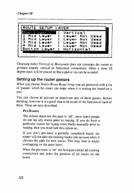
Chapter 20
R O U T E S E T U P L A V E R
I H i d L a u a r :2 1 ' l i d LaH€n :3 1 ' , f i d L a u e r :4 H i d L a u € r :B o t t o F t L a u e r :
U e r t i c e lL e u c n H o t U s e dL a U e r H o t U s t dL a u c r l t { o t U s e dL a u e r N o t U r e dH o r i z o n t a l
aI
Choosing either Vertical or Horizontal does not constrain the router toproduce exactly vertical or horizontal connections. Often a short 45degree track will be placed so that a pad or via can be avoided.
Setting up the router passesWhen you choose Netlist Route Route Setup you are presented with a listof 'passes' which the router can make when it is routing the board (or anet).
You can choose to activate or deactivate any of these passes. Beforedeciding, however it is a good idea to be aware of the function of each ofthem. These are now described.
Pre-Routes
The default status for this pass is 'off', since many peopledo not lay any tracks prior to routing. If you do have aparticular reason for laying some tracks manually prior torouting, then you must turn this option on.
If you don't pre-route a partially completed board, therouter will not, take the existing tracks into account when itchooses the path for new tracks. This may lead to tracksoverlapping on the same layer.
When the pre-route is 'on' the first pass checks all existingconnections and notes the position of all tracks on theboard.
122
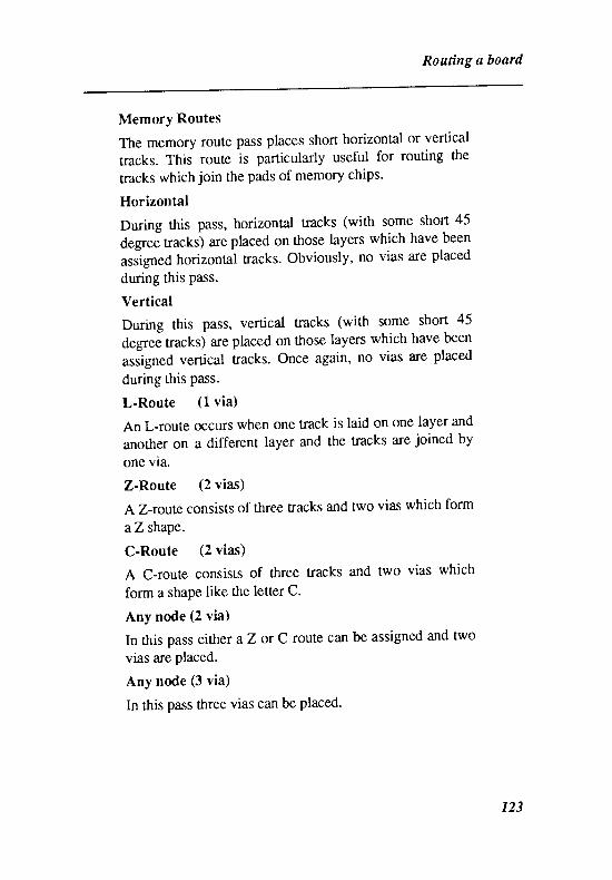
Routing a board
Memory Routes
The memory route pass places short horizontal or vertical
tlacks. This route is particularly useful for routing the
tracks which join the pads of memory chips'
Horizontal
During this pass, horizontal tracks (with some short 45
degree tracks) are praced on those layers which have been
urrign"d horizontal tracks. Obviously, no vias are placed
during this pass.
Vertical
During this pass, vertical tracks (with some short 45
degree tracks) are placed on those layers which have been
assigned vertical tracks. once again, no vias are placed
during this pass.
L-Route (1 via)
An L-route occurs when one track is laid on one layer and
another on a different layer and the tracks are joined by
one via.
Z-Route (2 vias)
A Z-route consists of three tracks and two vias which form
aZ shape.
C-Route (2 vias)
A C-route consists of three tracks and two vias which
form a shape like the letter C.
Any node (2 via)
In this pass either azor c route can be assigned and two
vias are placed.
Any node (3 via)
In this pass three vias can be placed.
123
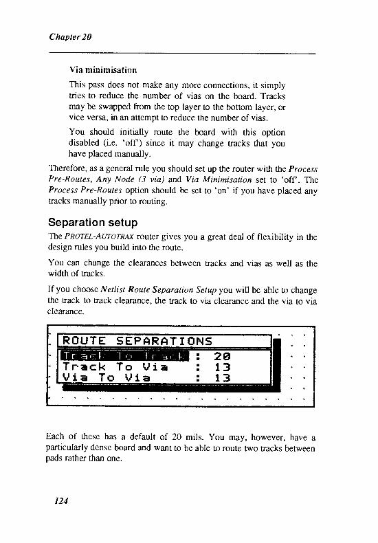
Chapter 20
Via minimisation
This pass does not make any more connections, it simplytries to reduce the number of vias on the board. Tracksmay be swapped from the top layer to the bottom layer, orvice versa, in an attempt to reduce the number of vias.
You should initially route the board with this optiondisabled (i.e. 'off) since it may change tracks that youhave placed rnanually.
Therefore, as a general rule you should set up the router with the Proce"s.tPre-Routes, Any Node (3 via) and Via Minimisation set !o 'off. TheProcess Pre-Routes option should be set to'on' if you have placed anytracks manually prior to routing.
Separation setupThe Pnors,t-Arnornex router gives you a great deal of flexibility in thedesign rules you build into the route.
You can change the clearances between tracks and vias as well as thewidth of tracks"
If you choose Netlist Route Separation Setup you will be able to changethe rack to track clearance, fhe track to via clearance and the via to viaclearance.
R O U T E S E P A R A T I O I { 5
T r e c k T o U i aU i a T o U i a
I
t
I
t
tI
2 gt 31 3
Each of these has a default of 20 mils. You may, however, have aparticularly dense board and want to be able to route two ffacks betweenpads rather than one.
124
Routing u board
Assume that you have 50 mil pads placed 100 mils apart. This gives a
clearance of 50 mils between pad edges. A 12 mil track with a 13 mil
separation means that only one track will fit between pads and still obey
the design rules.
Change each of the separations to 10 mils and change the track width (in
Variable Setup) to t0 mils. The tracks are now narrow enough for two to
fit between the pads with the required 10 mil separation!
Setting the router variablesThe Netlist Route Variable Setup option allows you to change three
important variables which affect the routing of a board; the route grid
size, ttre track size and the via size.
The default route grid size is set to 25 mils. This provides a track-to-
track clearance of 13 mils if 12 mil tracks are being placed. If you
require a greater separation choose a larger figure"
The default rack size is set to 12 mils. If you need two tracks to be laid
between 50 mil pads, change the track size to l0 mils and the track
separation to l0 mils.
You can change the size of vias which are placed during routing. The
default size is 50 mils.
Routing the boardThe Netlist Route Board is the most powerful of the routing options.
With it you can route a panially completed board or an entire board
using a previously created netlist.
The process is best explained via an example, so at this stage you shouldgo through the exercise of routing the demonstration PCB supplied on
the Library disk.
Before you begin a route make sure you have completed four tasks.
l. Check each of the Netlist Route setup options to make sure that
the track size and the clearances are correct. In this case you
can accept each of the default values.
t2s
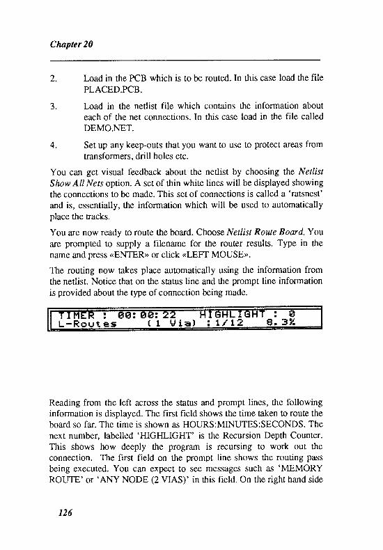
Chapter 20
2. Load in the PCB which is to be routed. In this case load the filePLACED.PCB.
3. Load in the netlist file which contains the information abouteach of the net connections. In this case load in the file calledDEMO.NET.
4. Set up any keep-outs that you want to use to protect areas from
transforrners, drill holes etc.
You can get visual feedback about the netlist by choosing the NetlistShow All Ners option. A set of thin white lines will be displayed showingthe connections to be made. This set of connections is called a 'ratsnest'
and is, essentially, the information which will be used to automaticallyplace the tracks.
You are now ready to route the board. Choore Netlist Rowe Board. You
are prompted to supply a filename for the router results. Type in thename and press <ENTER>> or click <LEFT MOUSE>>.
The routing now takes place automatically using the information fromthe netlist. Notice that on the status line and the prompt line informationis provided about the type of connection being made.
Reading from the left across the status and prompt lines, the followinginformation is displayed. The first field shows the time taken !o route theboard so far. The time is shown as HOURS:MINUTES:SECONDS. Thenext number, labelled 'HIGI{LIGHT' is the Recursion Depth Counter.This shows how deeply the program is recursing to work out theconnection. The first field on the prompt line shows the routing passbeing executed. You can expect to see messages such as 'MEMORY
ROUTE' or 'ANY NODE (2 VIAS)' in this field. On the right hand side
126
I I I l l - t \ I
L - R o u t e g,I
I V i a l : L f L z: E
g. 3'A

Routing a board
is ttre ratio of the number of nets paced to the total number of nets and
then the same figure given as a percentage. The higher this figure the
closer the router is to placing all tracks.
The router takes each net from the netlist and attempts to make a
connection for each of the passes which have been activated. The normal
order for the passes is as follows:
Memory routes
Horizontal
Vertical
L-routes
Z-routes
C-routes
Any node (2 vias)
3 vias
Any node (3 vias)
Each of these is explained in the section above entitled'Setting up the
Router Passes'.
As the routing progesses you will see thin horizontal and vertical lines
flashing on the screen showing you where the router is attempting toplace Facks. It is interesting to watch the strategy adopted by the router
during the Z-route and the C-route stages.
If you want to intemrpt the router at any stage, press any key (except the<<ENTER> key) or click <RIGHT MOUSE>>. A window will open askingyou to 'CONFIRM ABORT ROUTER'. Choose Yes to finish routing
and No to continue. An automatic save is carried out at the end of therouting pass.
When the route has been completed or the router cannot place any more
tracks the message 'AUTO-ROUTER FINISI{ED' will appear in awindow at ttre top of the screen. Note the percentage complete value atthe right hand side of the status line so that you know how many netsyou need to place manually.
127
Chapter 20
Press <ENTER>> or click <LEFT MOUSE> to continue. The route menureappears.
Now you are faced with the problem of what to do with the remainingnets which must be routed. There are a number of approaches you canadopt.
The first thing that you should do is check the board for obvious areas ofcongestion. You may have placed a component in an unsuitable place.The first step in overcoming this problem is to return to the unroutedPCB and move the key component in that area to a different part of theboard. Don't be afraid to experiment - it does not take very long to re-route a board in the majority of cases!
If that does not produce a satisfactory result move other componentswhich may free up the congested area and try again. Eventually you willreach a stage where the only remaining action is manual routing.
You should manually re-route before you attempt the Via Minimisationpass because this pass may change tracks from the top to bottom layerand vice versa. This action may tend to block out some of the possiblemanual routes. Also it can reduce the number of nodes which you canconnecl to.
Remember when you are manually routing the remaining connertionsthat you should maintain conventions such as laying tracks horizontallyon the top layer and vertically on the bottom layer.
Rout ing a s ingle connect ionChoose Netlist Route Connection to route a particular connection whichyou have highlighted using Netlist Slnw Nets. The message 'SELECT
CONNECTION' is displayed on the prompt line. You should then movethe cursor to the connection you want to route, then press <ENIER>> orclick <LEFT MOUSE>>.
The router then takes over and performs each of the passes that you haveenabled.
If it is possible, the connection will be routed. The prompt 'SELECT
CONNECTION' now indicates that you can route another connection.Press <ENTER>> or click <LEFT MOUSE> to return to the router menu.
128
Routing a board
Routing a connection manuallYIf you want to route a connection manually choose Netlist Route
Manu,a/. you often need to choose this option after an automatic route
which has not achieved l00Vo completion.
you are prompted to 'SELECT CONNECTION'. Move the cursor to the
highlighied connection and press <ENTER>> or click <LE[T MOUSE>).
The message 'PLACE TRACK' now appears on the prompt line. A rack
will be laid from the closest node to the cursor position when you press
<<ENTER>> or click <LEFT MOUSE>>. You will notice that the cursor is'tied' to the connection highlight to ensure that you connect the tracks to
the correct pads.
A via will be placed every time you change layers with lhe <<*r, key if the
Via Mode Auto oPtion is set t0 'on'.
The .PLACE TRACK' prompt continues to appear until the connection
has been fully routed.
Routing a netchoose Netlist Route Net to route a named net rather ttran a connection.you will be asked to enter the name of the net (or you can choose it from
a list if you enter a <<?rr). Once the net is chosen, the process is identical
to that for Netlist Route Connection-
Using the pad to Pad routerTo route a connection between two pads automatically, choose Netlist
Route Pad to Pad. The message:
ROUTE: SELECTFIRSTPAD
appears. Point to the flrst pad you need !o connect and press <<ENTER>>
or click <LEFT MOUSE>>.
The message now changes to:
ROUTE: SELECT SECOND PAD
Move !o the second pad and press <ENTER>> or click <LEFT MOUSE>>.
129

Chapter 20
The router now takes over and determines a path for the Facks.Sometimes it will also place a via to route that track to the ottrer side ofthe board. When it has tinished placing tracks you will be prompted toselect the first pad for the next route. Choose another pad if you want toroute another connection. If you have finished routing, press <ESC> orclick (RIGHT MOUSE>> to exit from the Pad to Pad routine.
r30
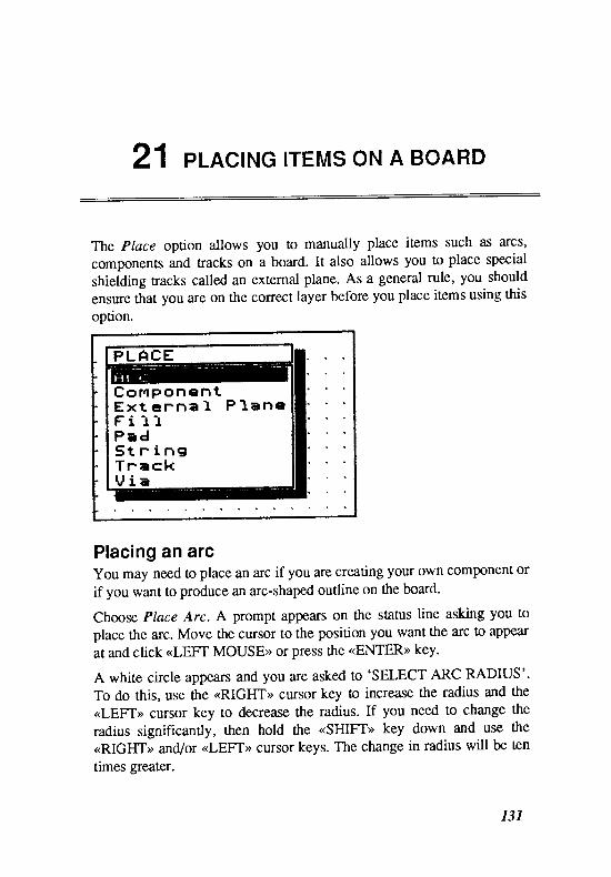
21 PLAcING lrEMs oN A BoARD
The place option allows you to manually place items such as arcs'
components and Eacks on a board. It also allows you to place special
shielding tracks called an external plane. As a general rule, you should
ensure that you are on the correct layer before you place items using this
option.
P L A C E
C o H p o n e n tE x t e r * n a l P l a n eF i 1 1P e d5 t r i n gT r a c k
a a
Placing an arcyou may need to place an arc if you are creating your own component or
if you want to produce an arc-shaped outline on the board.
Choos e Place Arc. A prompt appears on the status line asking you to
place the arc. Move the cursor to the position you want $re arc to appear
at and click <LEFT MOUSE>> or press the <ENTER> key.
A white circle appears and you are asked to 'SELECT ARC RAD[US'.
To do this, use the <<RIGHT> cursor key to increase the radius and ttre
(<LEFT> cursor key to decrease the radius. If you need to change the
radius significantly, then hold the <SHIFT>> key down and use the
<RIGHT, and/or <<LEFT>> cursor keys. The change in radius will be ten
times greater.
131
Chapter 2I
When you have the radius you require, press <ENTER>> or click (LEFT
MOUSE>), and you are then prompted to select the arc segments. Thecircle is divided into four segments. One is from 12 o'clock round to 3o'clock and is under the control of the (<uP>> cursor key. The next isfrom 3 o'clock to 6 o'clock and is under the control of the <RIGHT>cursor key. The 6 to 9 segment is controlled by the <DOWN> key andthe remaining segment is controlled by the <LEFT> key. Pressing any ofthese keys results in that segment of the arc being deleted. Pressing ttresame key again restores the deleted segment.
As an example, if you want an arc which extends from 3 o'clock aroundto 9 o'clock in the clockwise direction, press the (<LEFT> key and the(<IJP)> key.
When you press (ENTER>> or click <LEFT MOUSE> you are given anopportunity to move ttre arc if it is not positioned correctly.
Placing a componentWhen you choose Place Component you are prompted to indicate whereyou want to place the component. Move the cursor to the place requiredand click (LEFT MOUSE>> or press (ENIER>). An input window opensasking you to enter the name of the component. If you have not yetplaced a component ttre window contains a question mark.
You can now type in the component name or else press <ENIER>> orclick <LEFT MOUSE>> to see the list of components which are available.
Move the selection bar to the required component. If the componentdoes not appear in ttre window press <PGDN> to see more. Press<ENTER>> or click <LEFT MOUSE>> to select the component.
The prompt:
COMPONENT DESIGNATOR
appears.
You must now supply a component designator. A component designatorusually consists of a letter such as C or J or R followed by a number.Thus you may decide to call an edge connector J3 or a capacitor C4. Ifyou do not supply a designator Pnornt-Atnornur will assign one
r32
Placing items on a board
starting at Al then M and so on. If you specify a designator which
already exists the message:
COMPONENT DESIGNATOR IS ALREADY USED
appears.
After you supply the designator you are asked to input a comment.
Remember that any comments will appear on the layer selected in Setup
Component Text.It is a good idea to keep them as short as possible.
Once you have entered the comment the prompt:
MOVING COMPONENT
appears. The component can now be moved to another position if
required. For details of how to rotate the component refer to page 66.
When it is in the correct position press <<ENTER> or click <LEFT
MOUSE>>.
Note that when you have placed the component, you are prompted to
place the next one. If you do not wanf to place another component press
<<ESC> or click <RIGHT MOUSE> to exit from the option.
Creating an external planeIf you need to provide exra shielding on a particular layer (perhaps to
conform to local RF emission standards) then it is possible to fill an area
with cross-hatched wide tracks even if that area has already been
routed.
Choose Place External Plane. The message:
SELECT START POINT ON POLYGON
appears on the prompt line. You can now define any areil in the shape of
a regular or inegular or convex or concave polygon to be filled. Press<ENTER>> or click <LEFT MOUSE>> to start defining the polygon.
Now the prompt changes to:
SELECT POINT ON POLYGON
and you can now indicate each of the vertices of the polygon. When you
have finished marking the polygon press <ESC> or click <RIGHT
MOUSE>>.
133
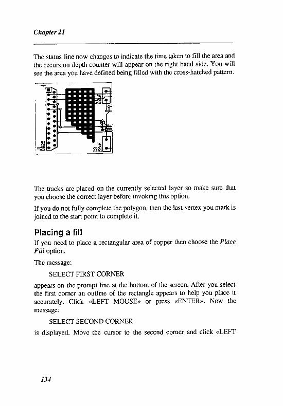
Chapter 2I
The status line now changes to indicate the time taken to fill the area and
the recursion depth counter will appear on the right hand side. You will
see the area you have defined being filled with the cross-hatched pattern.
The tracks are placed on the currently selected layer so make sure that
you choose the correct layer before invoking this option.
If you do not fully complete the polygon, then the last vertex you mark isjoined to the start point to complete it.
Placing a f i l lIf you need to place a rectangular area of copper then choose the Place
Fill option.
The message:
SELECT FIRST CORNER
appears on the prompt line at the bottom of the scr@n. After you select
the first corner an outline of the rectangle appears to help you place it
accurately. Click <LEFT MOUSE> or press <ENIER>>. Now the
message:
SELECT SECOND CORNER
is displayed. Move the cursor to the second corner and click <LEFT
r34

Placing items on a board
MOUSE>> or press <<EI{fER>>. As soon as you select the second cornerthe rectangular area is filled.
If you select the second corner in the same place as the first corner youwill hear a beep and you will be asked to respecify both the first andsecond corners again.
Placing a padTo place a pad, select the Place Pad option and move the cursor to therequired position on the board then click <LEFT MOUSE> or press<ENTER>>.
The shape of the pad which is placed on the board is determined by the
setting in the Current menu. The default type is called Roun d62. If you
require a pad of a different shape (say, a square pad), then change it in
the Current menu and then go back to the Place menu. You can alsochoose Moire or Cross-Hair targets to help you line up plots.
Remember that pads belong to every layer, therefore you do not have toworry about which layer you are on before placing a pad.
Placing a str ingTo place a string choose the Place String option. A window opens whichallows you to enter the string to be placed. Enter the string then press<ENTER>> or click <LEFT MOUSE>>.
The sring appears on the board in inverse and you can now move it tothe place required. Use the cursor keys or the mouse. For details of how
to rotate the string refer to page 66.
The size of the string depends on the settings in the Currenr menu.
After the string is placed you get ttre opportunity to specify another.When you have finished placing strings, click <RIGHT MOUSE> orpress (<ESC>>.
Placing tracksIndividual connections can be laid by using the Pad to Pad routingoption in the Ne tlist Route menu. If, however, you need to lay tracksmanually for some reason then choose Place Track.
1 3 5
Chapter 2I
The message:
SELECT TRACK START POINT
is displayed on the prompt line. Move to the point where you want the
track to begin and press <ENIER> or click <LEFT MOUSE>>. Now
when you move the mouse or use the cursor keys a thin line is drawn
outlining where the track will be laid. When the cursor is at the point thatyou want to lay the rack press <ENTER> or click <LEFT MOUSE>>.The track is drawn at the width specitied in the Current menu.
If you now move the cursor to a different position the track will becontinued, and so on. If you click <RIGHT MOUSE>> or press (<ESC>)
then you can move to a different spot on the board and lay another [ack.
To stop laying tracks press (<ESC>) or click <RIGHT MOUSE>> when theprompt 'SELECT TRACK START POINT' appears.
Tracks can only be drawn as vertical, horizontal or 45 degree diagonallines. This has been set as it is regarded as god practice in the industry
to only draw tracks this way. If, however, you need to draw a track atsome other angle, select the Currenr menu and set the Toggle OrthoMode option to 'off before you lay the lrack.
Placing a v iaThe process for placing a via is identical to that for placing a pad.
Simply choose Place Via and move to the place where you want to place
the via then press (<ENIER>> or click <LEFT MOUSE>). The size of thevia is determined by the setting in the Current menu.
136
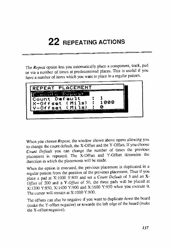
ah al\
REPEATING ACTIONSZZ REPEATING A
| ! :
The Repear option lets you automatically place a component, track, pad
or via a number of times at predetermined places. This is useful if you
have a number of items which you want to place in a regular pattern.
f f i P L A C E H E N T
C o u n t D e f a u l t tt I
I A g EaH - 0 f f s t t ( H i l s ) :
Y - O f f s e t ( H i l s l !
when you choose Repear, the window shown above opens allowing you
to change the count default, the X-Offset and the Y-Offset- If you choose
count bryoutt you can change the number of times the previous
placement is repeated. The X-Offset and Y-Offset determine the
Oirection in which the placements will be made.
When the option is executed, the previous placement is duplicated in a
regular putt.* from the position of the previous placement. Thus if you
place a pad at X:1000 y:g00 and set a count Default of 3 and an X-
offset oi 200 and a y -offset of 50, the rhree pads will be placed at
X:1200 y:g50, X:1400 y:goo and X:1600 Y:950 when you execute it.
The cursor will remain at X:1000 Y:800'
The offsets can also be negative if you want to duplicate down the board
(make the y-offset negative) or towards the left edge of the board (make
the X-offset negative).
137
Chapter 22
To implement a rep%t operation choose Repeat Execute Repeet. Youwill be prompted tc enter the Count Default again just to make sure thatyou really want to repeat the operation the number of times you havespecifred. You are then prompted to:
CONFIRM MULTIPLE REPEAT PLACE
Choose Y es to execute the repeat and No to return to the Repeaf menu.
If you use the Repeat option to copy a track, you should be aware thatonly the last track placed will be copied. The option does not allow youto copy an entire connection. If you want to copy a set of tracks, use theH i g hli g ht D uplic ate option.
r38
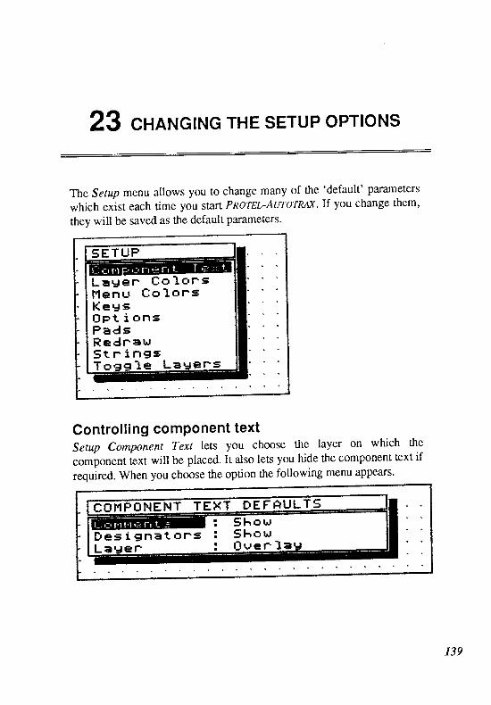
23 cHANGING THE sETUP oPrloNs
The Setup menu allows you to change many of the 'default' parameters
which exist each time you start Pnorg,t-Atnornex. If you change them,
they will be saved as the default parameters.
S E T U P
L a g e r C o l o r sl ' f enu Co lo rsK e t l gO p t i o n gP a d sR e d r E r r ,S t r i n g sT o g g l e L a H e r s
Controll ing component textSetup Component Text lets you choose the layer on which the
component text will be placed. It also lets you hide the component t,ext if
required. When you choose the option the following menu appears.
139
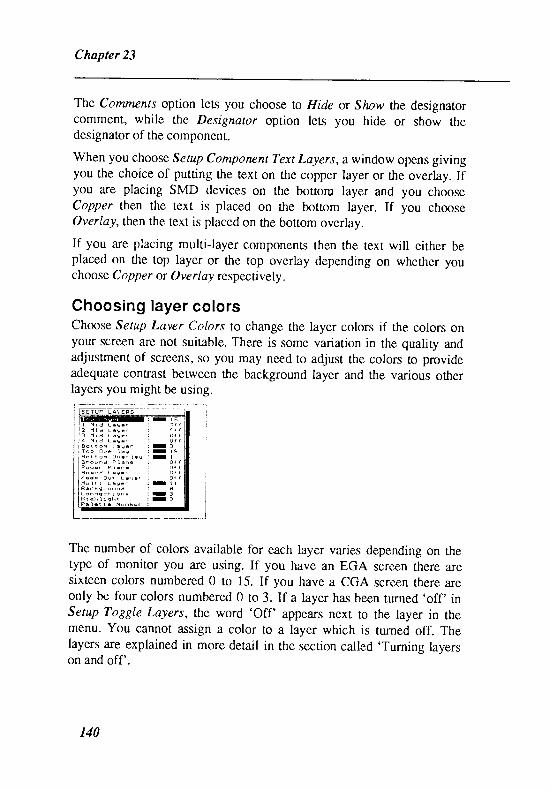
Chapter 23
The Commenrs option lets you choose to Hide or Show the designatorcomment, while the Designator option lets you hide or show thedesignator of the component.
When you choose Setup Component Text Layers, a window opens givingyou the choice of putting the text on the copper layer or the overlay. Ifyou are placing SMD devices on the bottom layer and you chooseCopper then the text is placed on the bottom layer. If you chooseoverlay, then the text is placed on the bottom overlay.
If you are placing multi-layer components then the text will either beplaced on the top layer or the top overlay depending on whether youchoose Copper or Overlay respectively.
Choosing layer colorsChoose Setup Layer Colors to change the layer colors if the colors onyour scre€n are not suitable. There is some variation in the quality andadjustment of screens, so you may need to adjust the colors to provideadequate conrast between the background layer and the various otherlayers you might be using.
The number of colors available for each layer varies depending on thetype of monitor you are using. If you have an EGA screen there aresixteen colors numbered 0 to 15. If you have a CGA screen there areonly be four colors numbered 0 to 3. If a layer has been turned 'off inSetup Toggle Layers, the word 'Off' appears next to the layer in themenu. You cannot assign a color to a layer which is turned off. Thelayers are explained in more detait in the section called 'Turning layerson and off'.
140
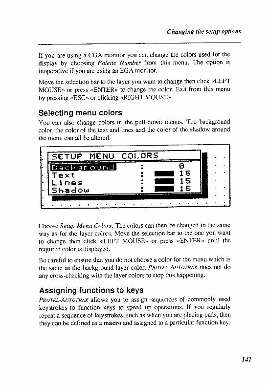
Changing the setup options
If you are using a CGA monitor you can change the colors used for the
display by choosing Palette Number from this menu. The option is
inoperative if you are using an EGA monitor.
Move the selection bar to the layer you want to change then click (LEFT
MOUSE>> or press <ENTER>> to change the color. Exit from this menu
by pressing <ESC>, or clicking <RIGI{| MOUSE>).
Selecting menu colorsYou can also change colors in the pull-down menus. The background
color, the color of the rcxt and lines and the color of the shadow around
the menu can all be altered.
SETup r ' fEnu coLons
T E X tL i n e sS h a d o h ,
It
ti
tt
II
III
g1 51 51 5
Choosesetup MenuColors. The colors can then be changed in the same
way as for the layer colors. Move the selection bar to the one you want
to change then click <.LEFT MOUSE> or press <<ENTER>) until the
required color is displayed.
Be careful to ensure that you do not choose a color for the menu which is
the same as the background layer color. Pnornr-Atnornat does not do
any cross-checking with the layer colors to slop this happening.
Assigning functions to keysPnoret-Atnornur allows you to assign sequences of commonly used
keystrokes to function keys to speed up operations. If you regularly
repeat a sequence of keystrokes, such as when you are placing pads, then
they can be defined as a macro and assigned to a particular function key.
I4l
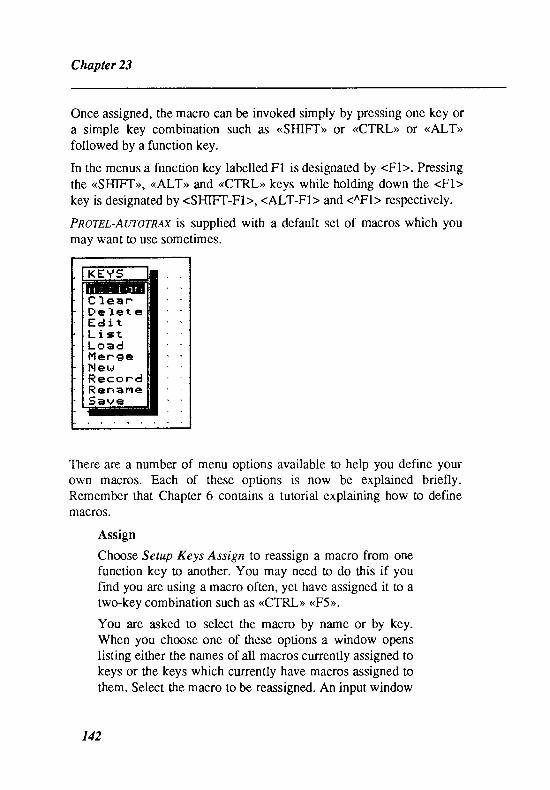
Chapter 23
Once assigned, the macro can be invoked simply by pressing one key ora simple key combination such as (<SHIFT>> or <<CTRL> or <<ALT>>
followed by a function key.
In the menus a function key labelled Fl is designated by <Fl>. Pressingthe <SHIFT>), (<ALT>> and <CTRL> keys while holding down the <F1>key is designated by <SHIFT-Fl>, <ALT-FI> and <^Fl> respectively.
Pnors,t-Awornatr ts supplied with a default set of macros which youmay want to use sometimes.
C l , e a rD e ] e t eE d i tL i s tL o a dJ ' f e rgeN e wR e c o r dR e n a m eS a v e
There are a number of menu options available !o help you define yourown macros. Each of these options is now be explained briefly.Remember that Chapter 6 contains a tutorial explaining how to definemacros.
Assign
Choose Setup Keys Assign to reassign a macro from onefunction key to another. You may need to do this if youtind you are using a macro often, yet have assigned it to atwo-key combination such as <CTRL>) <<F5>>.
You are asked to select the macro by name or by key.When you choose one of these options a window openslisting either the names of all macros curently assigned tokeys or the keys which currently have macros assigned tothem. Select the macro to be reassigned. An input window
142
Changing the setup options
opens asking you to select the function key to which themacro is to be assigned.
Press the function key or function key combination thatyou want to assign the macro [o.
You are returned to the selection window. If you havefinished assigning macros press <ESC> or click <RIGHTMOUSE>> to return to the Keys menu.
Clear
Choose the Setup Keys Clear option clear all macros fromthe memory. Although macros are cleared from thememory the disk file is not affected.
You are asked to confirm that you want to clear all keymacros. Choose Yes to clear the macros and No to leavethem intact.
Delete
Choose Delete tro delete one or more macros from thememory. The macros are not deleted from the .KEY fileunless you choose to save the new se"t of macros.
You are asked to select macros by name or by key. Onceyou have selected a macro that you want to delete you areasked to confirm the deletion. Choose Yes to proceed andNo to stop the macro being deleted.
Edir
Once you have defined a macro you can add to it or deleteparts of it. Select the macro that you want !o change andan edit window opens. The name of the macro and thefunction key it is assigned to is displayed at the top of thiswindow.
The window displays the representations of each of thekeystrokes that comprise the macro. If you press the<BACKSPACE> key you will delete items in the macro.If you press any other key you will add that keystroke tothe macro.
143

Chapter 23
You can press other function keys which themselvescontain macros at this stage.
Press (ENTER> or click <LEFT MOUSE> to finishediting the macro.
List
You can list the current macros by name or by key. Themacro names or key names are displayed in aninformation window.
Load
Choose this option by moving the selection bar tohighlight the word 'Load' then pressing <<ENTER> orclicking <LEFT MOUSE>>. The reason is that the Listoption also begins with L and is before Load in the list.
An input window opens with the default value of '*.KEY'.
To load a new key file either type in the name of the file,or press <ENTER>> or click <LEFT MOUSE>> to see a listof key files.
Select a file then a window opens asking you to confirmthat you want !o load it. Choose Yes to load and No toreturn to the Key menu without loading the file.
New
There are two methods you can use to define a new keymacro. The first is by choosing Ser up Keys New. An inputwindow opens and you can enter the name you want togive the new key macro. Another window then opensasking you to choose the key to which the macro will beassigned. A default value (which is the next available key)appears. If the default value is not acceptable, pressanother function key combination.
A macro edit window then opens allowing you to type inthe keystrokes that you want to assign. Press <<ENTER>> orclick <LEFT MOUSE>> to exit from this window. You arethen prompted to enter another new key macro name. If
144

Changing the setuP oPtions
you have finished defining macros press <ESC> or click(RIGHT MOUSE>>.
Record
The second method of defining a key macro is by
recording it. This option allows you to work through the
macro while seeing the effect each keystroke has on the
board. Mouse movements are not, recorded.
Choose Setttp Keys Record. You Ne prompted t0 supply a
nurme and a key as in the New option. You will ttren hear a
beep and you are returned to the board where you can then
simulate the set of keysEokes that you want to store in the
macro. When you have completed the keystrokes press
<CTRL>> <<END>> t0 turn the 'recorder' off. You are then
be returned to the Key menu.
Rename
Choose Setup Keys Rename to change the name of a
macro, rather than the key it is assigned to. You are
prompted to supply the name which you want to change
and then the name you want to change it to. If the name
you Ury to change it to already exists the message 'KEY
MACRO NAME ALREADY USED' is displayed.
Save
Once you have changed some macros or created one or
more new macros you will want to save them in a file so
that you can use them again. You can either save them
under the default name of TRAXEDIT.KEY or choose a
name of your own.
If you try to save them under a name that already exists
the warning:
KEY MACRO FILE EXISTS. OVERWRITE?
is displayed. Choose Yes to delete the existing macro file.
Otherwise choose No. You can then enter another name.
145
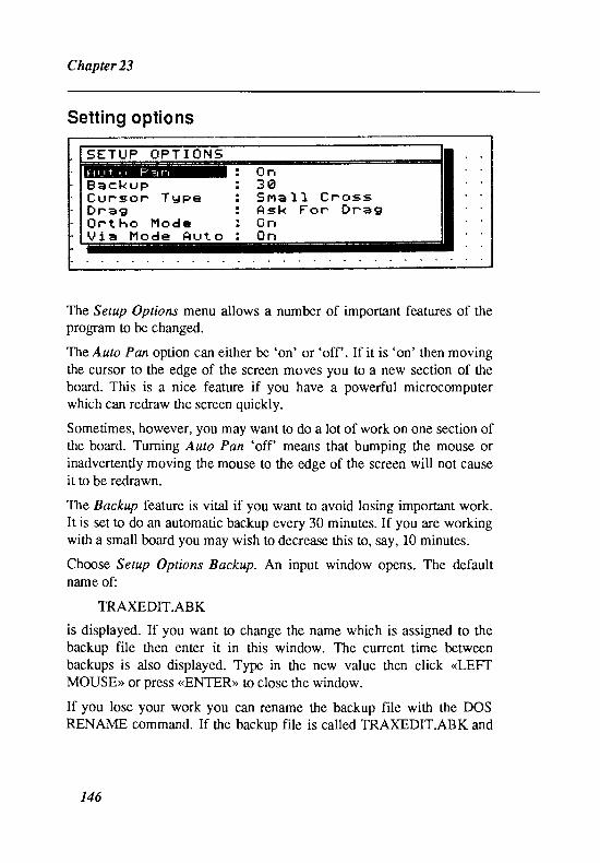
Chapter 23
Setting options
S E T U P O P T I O N s
B a c k u FC u r s o r T u l p eD n a g0r t ho l ' ' l odeU i a l ' l ode Au t o
O n3 A5 n ' r a 1 1 C n o s sA s k F o r D r e e lO nO n
The Setup Options menu allows a number of important features of theprogram to be changed.
The Auto Pan option can either be'on' or'off ' . If i t is'on'then movingthe cursor to the edge of the screen moves you to a new section of theboard. This is a nice feature if you have a powerful microcomputerwhich can redraw the screen quickly.
Sometimes, however, you may want to do a lot of work on one section ofthe board. Turnin g Auto Pan 'off' means that bumping ttre mouse orinadvertently moving the mouse to the edge of the screen will not causeit to be redrawn.
The Backup feature is vital if you want to avoid losing important work.It is set to do an automatic backup every 30 minutes. If you are workingwitlt a small board you may wish to decrease thiS to, sy, l0 minutes.
Choose Setup Options Backup" An input window opens. The defaultname of:
TRAXEDIT.ABK
is displayed. If you want to change the name which is assigned to thebackup file then enter it in this window. The current time betweenbackups is also displayed. Type in the new value then click <LEFTMOUSE>> or press <ENIER>> to close the window.
If you lose your work you can rename the backup file with the DOSRENAME command. If the backup file is called TRAXEDIT.ABK and
r46
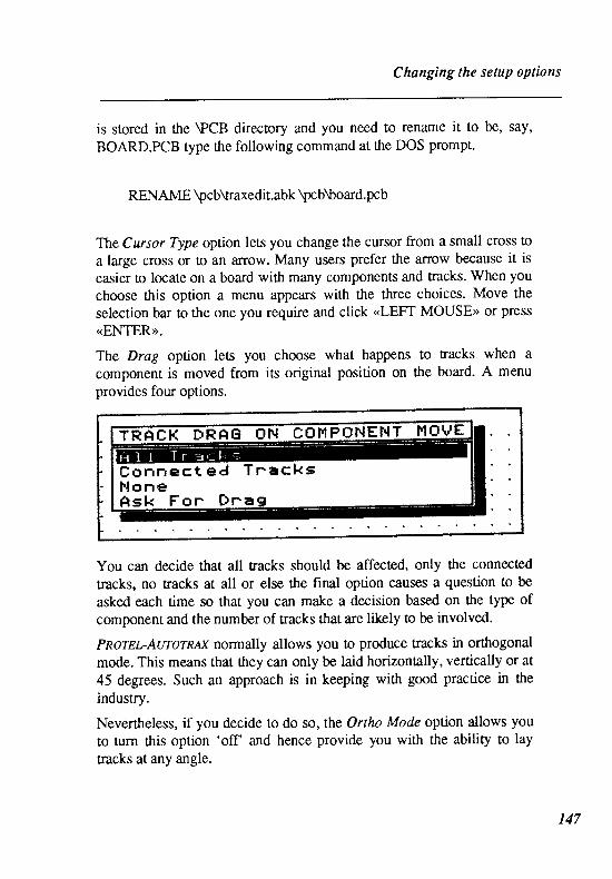
Changing the setup options
is stored in the \PCB directory and you need to rename it to be, say,
BOARD.PCB type the following command at the DOS prompt.
RENAME \pcb\naxedit. abk \pc b\board. pcb
The Cursor Type option lets you change the cursor from a small cross !o
a large cross or to an arrow. Many users prefer the arrow because it is
easier to locate on a board with many components and fracks. When you
choose this option a menu appears with the three choices. Move the
selection bar !o the one you require and click <LEFT MOUSE>> or press
<<ENTER>>.
The Drag option lets you choose what happens to tracks when a
component is moved from its original position on the board. A menu
provides four options.
dltEl'lr 1'f-0t/E
C o n n e c t e d T r a c k sI t l oneA s k F o r D r e
You can decide that all racks should be affecrcd, only the connected
tracks, no tracks at all or else ttre final option causes a question to be
asked each time so that you can make a decision based on the type of
component and the number of tracks that are likely to be involved.
Pnorst-Atnornur normally allows you to produce tracks in orthogonal
mode. This means that they can only be laid horizontally, vertically or at
45 degrees. Such an approach is in keeping wittr good practice in the
industry.
Nevertheless, if you decide to do so, the Ortho Mode option allows you
to turn this option 'off' and hence provide you with the ability to lay
tracks at any angle.
147
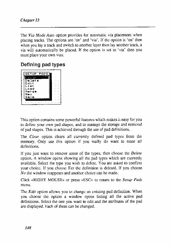
Chapter 23
The Via Mode Auto option provides for automatic via placement whenplacing Eacks. The options are 'on' and 'via'. If the option is 'on' thenwhen you lay a track and switch to another layer then lay another track, avia will automatically be placed. If the option is set to 'via' then you
must place your own vias.
Defining pad types
ffirffirl FFii'" llI L i s tI l . oad l l| il:;""l save j l l--
This option contains some powerful features which makes it easy for youto define your own pad shapes, and to manage the storage and retrievalof pad shapes. This is achieved through the use of pad definitions.
The Clear option clears all currently defined pad types from thememory. Only use this option if you really do want to erase alldefinitions.
If you just want to remove some of the types, then choose the Deleteoption. A window opens showing all the pad types which are curentlyavailable. Select the type you wish to delete. You are asked to confirmyour choice. If you choose Yes the definition is deleted. If you chooseNo the window reappears and another choice can be made.
Click <RIGHT MOUSE>> or press <ESC> to return to the Setup Padsmenu.
The Edit option allows you to change an existing pad definition. Wheriyou choose the option a window opens listing all the active paddefinitions. Select the one you want to edit and the attributes of the padare displayed. Each of these can be changed.
148
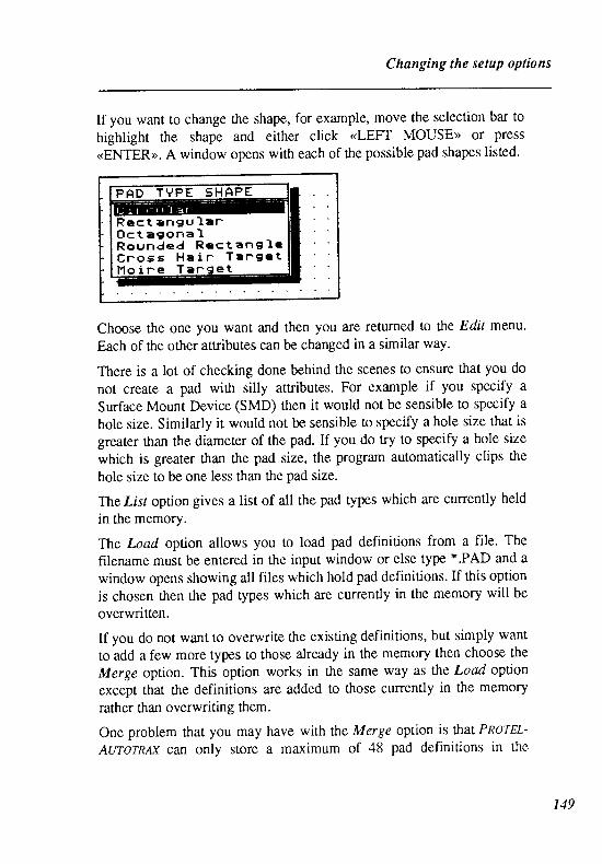
Changing the setup options
If you want to changehighlight the shape<<ENTER>>. A window
the shape, for example, move the selection bar to
and either click <LEFT MOUSE> or press
opens with each of the possible pad shapes listed.
P A O T V P E 5 H A P E
R e c t a n E u l a rO c t a g o n a IR o u n d e d R e c t a n g l eC r o s s H e i n T e n g e tl ' l o i n e T a r g e t
Choose the one you want and then you are returned to the Edir menu.
Each of the other attributes can be changed in a similar way.
There is a lot of checking done behind the scenes to ensure that you do
not create a pad with silly attributes. For example if you specify a
Surface Mount Device (SMD) then it would not be sensible to specify a
hole size. Similarly it would not be sensible [o specify a hole size that is
greater than the diameter of the pad. If you do try to specify a hole size
which is greater than the pad size, the program automatically clips the
hole size to be one less than the pad size.
The List option gives a list of all the pad types which are cunently held
in the memory.
The Load option allows you to load pad definitions from a file. The
filename must be entered in the input window or else type *.PAD and a
window opens showing all files which hold pad definitions. If this option
is chosen then the pad types which are currently in the memory will be
overwritten.
If you do not want to overwrite the existing definitions, but simply want
to add a few more types to those already in the memory then choose the
Merge option. This option works in the same way as the Load option
except that the definitions are added to those currently in the memory
rather than overwriting them.
One problem that you may have with the Merge option is that Pnortu
Aurornur can only store a maximum of 48 pad definitions in the
r49
Chapter 23
memory at one time. Thus if you are going to merge a file you must beconfident that the total of the definitions in the memory and those in thetile does not exceed 48.
The New option allows you to define a completely new pad definition.When you choose the option you are asked to supply a name for the newdefinition. Once again, you must first ensure that there are not already 48in the memory.
Enter the name and click (<LEFT MOUSE> or press (ENTER>>. Awindow opens showing the possible attributes of the pad. These willhave been supplied from the definition which is shown as the default inthe Current menu.
The process of defining the type of pad is exactly the same as that forediting a pad. Simply move the selection bar to highlight the attributesthat require changing and select the new ones.
The final option allows you to Save your pad definitions. Choose SetupPads Save. Enter a name for the file and either click <LEFT MOUSE>or press <<ENTER>>. The file is saved with a .PAD extension.
Choosing the redraw qualityThis option allows you to choose the quality of each redraw for arcs,fills, pads, strings, tracks and vias. Each one can be set to either draft orfinal.
Setting string defaultsThe term string refers to the characters that are used as comments andcomponent designators as well as the free text that can be placed on aboard.
The default value for each is 60, but it is possible to change each bytyping in a value up to 1000. A maximum value which is greater than560 mils is not recommended.
rs0
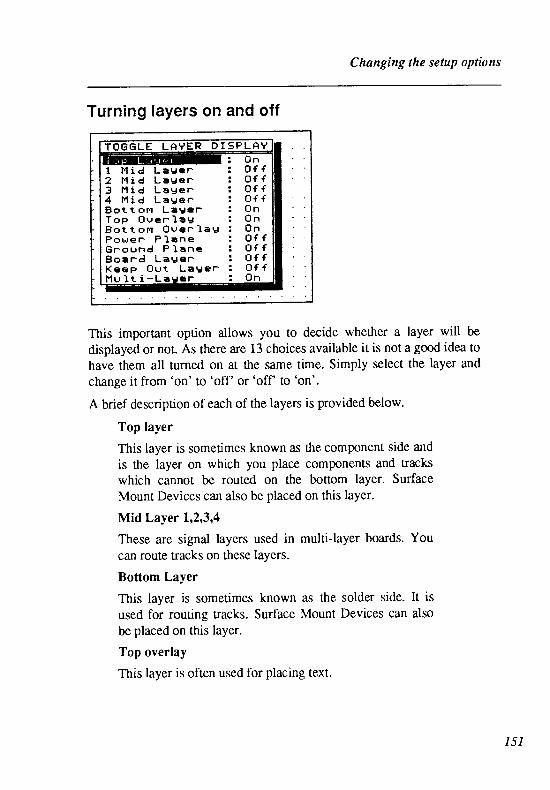
Changing the setup options
Turning layers on and off
T O G G L E L A V E R D I s P L A Y
l ' l u 1 t i - L e g e r
O no f fo f fo f f0 f f0 nO nO no f fo f fo f f0 f fO n
I l , l i d L a s c r2 l ' f i d L a l l e r3 l ' l i d L a l J e F4 ] ' l i d L a u e nB o t t o l , r L a g e rT o p O v e r l a gB o t t o m O v e r l a gP o w e r P l a n eG r o u n d P l e n cB o e r d L a u e rK e e p O u t L a u e r
This important option allows you to decide whether a layer will be
displayed or nol As there are 13 choices available it is not a good idea to
have them all turned on at the same time. Simply select the layer and
change it from 'on' to 'off' or 'off [o 'on'.
A brief description of each of the layers is provided below.
Top layer
This layer is sometimes known as the component side and
is the layer on which you place components and tracks
which cannot be routed on the bottom layer. Surface
Mount Devices can also be placed on this layer.
Mid Layer lr2r3r4
These are signal layers used in multi-layer boards. You
can route tracks on these layers.
Bottom Layer
This layer is sometimes known as the solder side. It is
used for routing tracks. Surface Mount Devices can also
be placed on this layer.
Top overlay
This layer is often used for placing text.
t5I
Chapter 23
Bottom overlay
This layer is used for text which may be necessary to
explain features on the solder side.
Ground Plane
The ground plane is the plane which is used to shield
sensitive sections of the circuit and to minirn tze radiated
energy. It is a separate plane of copper sandwiched
between the other layers. There are holes in the copper
wherever leads pass through to other layers so that they do
not contact with,the copper.
Power plane
The power plane is very similar to the ground plane. It is
used when large curents are needed.
Board layer
The board layer provides a similar function to the keep out
layer. It is used, for example, when you want to show the
edges of the board in a plot, but do not want to plot all the
ottrer'keep outs'.
Keep out layer
This is a very important layer which is used to define keep
out areas on the board. It is often used to define the limits
of the board. To do this, turn the keep out layer on and
select that layer by pressing the <<+>> key on the keypad.
Now lay tracks right around the limit of the board. Since
the keep out layer affects every layer, the router will not
be able to place tracks outside this border.
You can also define keep out areas in places where you
want to drill through the board.
Multi-layer
With this layer you can define the color for multi-layeritems such as pads and vias.
152
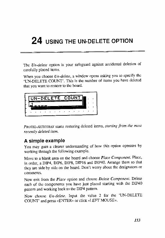
24 ustNc THE uN-DELETE oPTloN
The (Jn-delete option is your safeguard against accidental deletion of
carefully placed items.
When you choose Un-delete, a window opens asking you to specify the.LIN-DELETE COUNT'. This is the number of items you have deleted
that you want to restore to the board.
f f iTE COUNrI
pnornr-Autornur smrts restoring deleted iteffis, starting from the most
recently deleted item.
A simple exampleyou may gain a clearer understanding of how this option operates by
working through the following example.
Move to a blank area on the board and choose Place Component. Place,
in order, a DIP4, DIP6, DIP8, DIP16 and DIP40. Arrange them so that
they are side by side on the board. Don't worry about the designators or
comments.
Now exit from the Place optLon and choose Delete Component. Delete
each of the components you have just placed starting with the DIP40
pattern and working back to the DIP4 pattern.
Now choose Un-detete. Input the value 2 for the 'LIN-DELETE
COTINT' and press <ENTER>> or click (LEFT MOUSE>>.
rs3

Chapter 24
You will see that the DIP4 and DIPS patterns have been restored becausethese were the two that were deleted most recently.
Now choose Un-delete again. This time specify an 'LIN-DELETE
COLTNT' of 1. The DIPS pattern will now be restored.
The 'stack' of deleted items is capable of storing up to 5000 items.
r54
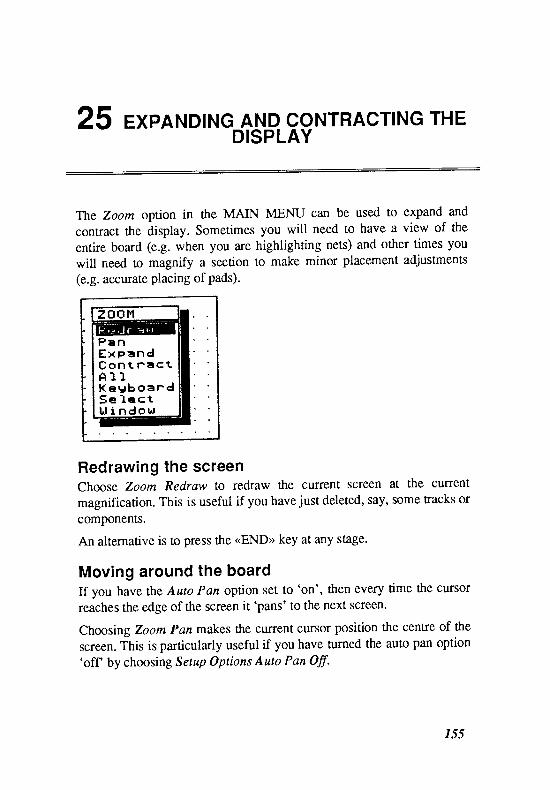
^-, r' )^ EXpANDING AND CoNTRACTING THE---.-., fI - f7 =XPANI
DISPLAY
The Zoom option in the MAIN MENU can be used to expand and
contract the Oisplay. Sometimes you will need to have a view of the
entire board (e.g. when you are highlighting nets) and other times you
will need to magnify a section to make minor placement adjustments
(e.g. accurate placing of Pads).
zaoFl
P e nE x p a n dC o n t F e c tf i 1 1K e u b o a r d5 e l e c tU i n d o t l
Redrawing the screenChoose Zoom Redraw to redraw the current screen at the current
magnification. This is useful if you have just deleted, So!, some tracks or
components.
An alternative is to press the <END> key at any Stage.
Moving around the boardIf you have the A uto Pan option set [o 'on', then every time the cursor
reaches the edge of the Screen it 'pans' to the next Screen.
Choosing Zoom Pan makes the current cursor position the centre of the
screen. This is particularly useful if you have turned the auto pan option'off by choosing Setup Options Auto Pan Off.
15s
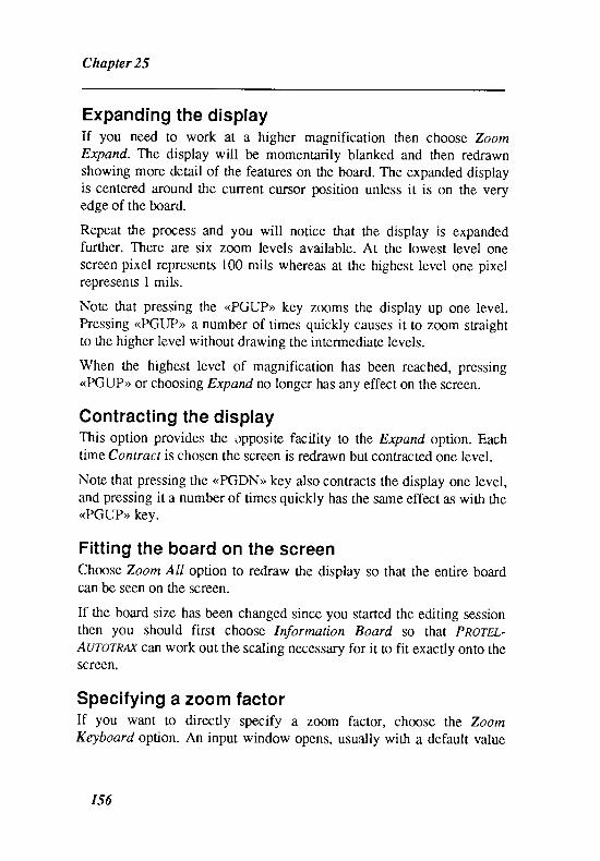
Chapter 25
Expanding the displayIf you need to work at a higher magnification then choose ZoomExpand. The display will be mornentarily blanked and then redrawnshowing more detail of the features on the board. The expanded displayis centered around the current cursor position unle.ss it is on the veryedge of the board.
Repeat the process and you will notice that ttre display is expandedfurther. There are six zoom levels available. At the lowest level onescreen pixel represents 100 mils whereas at the highest level one pixelrepresents I mils.
Note that pressing the <PGUP> key zooms the display up one level.Pressing "PGUP>) a number of times quickly causes it to zoom sraightto the higher level without drawing the intermediate levels.
When the highest level of magnification has been reached, pressing<PGUb) or choosing Expand no longer has any effect on the screen.
Contracting the displayThis option provides ttre opposite facility to the Expand option. Eachtime Contracf is chosen the screen is redrawn but contracted one level.
Note that pressing the <PGDN> key also contracts the display one level,and pressing it a number of times quickly has the same effect as with ttre<PGUP> key.
Fitt ing the board on the screenChoose Zoom AII option to redraw the display so that the entire boardcan be seen on the screen.
If the board size has been changed since you started the editing sessionthen you should first choose Inforrnntion Board so that Pnorrt-Aurornur can work out the scaling necessary for it to fit exactly onto thescreen.
Specifying a zoom factorIf you want to directly specify a zoom factor, choose the ZoomKeyboard option. An input window opens, usually with a default value
rs6
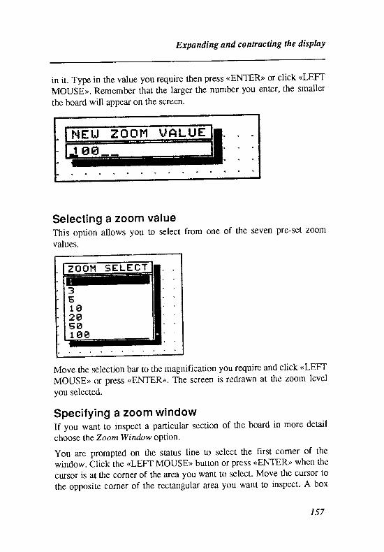
Expanding and contracting the display
in it. Type in the value you require then press <ENTER>> or click <LEFT
MOUSE>). Remember that the larger the number you enter, the smaller
the board will appear on the screen.
Selecting a zoom valueThis option allows you to select from one of the seven pre-set zoom
values.
Move the selection bar to the magnification you require and click <LEFT
MOUSE>> or press <ENIER>). The screen is redrawn at the zoom level
you selected.
Specitying a zoom windowIf you want to inspect a particular section of the board in more detail
choose the ZoomWind.ow oPtion.
you are prompted on the status line to select the first corner of the
window. Click the <<LEFT MOUSE> button or press <ENTER>> when the
cursor is at the corner of the area you want to select. Move the cursor to
the opposite corner of the rectangular area you want to inspect. A box
a t l
a i t
i a ' l
l , lEU ZOOI' f U f f L U E
J E g
Zoot ' t 5ELEtrT
351 B2 g5 g1 6 8
157

Chapter 25
appeus outlining the window. The prompt now reads 'SELECT
SECOND CORNER'. Click the <<LEFT MOUSE> button or press<ENTER>> to select the second corner.
The window now zooms to fill the screen.
r58

I.]TILITIES SECTION


26 ustNc THE TRAXPLITPRocRAM
The TRAXPLOT program has been designed to allow you to produce
quality artwork using a conventional pen plotter or a photoplotter and to
produce draft quality check plots. It also allows you to produce files
which will drive Gerber photoplotters and Excellon NC Drills.
One of the features of this program is that the external protection device
is not required. This allows you !o use the program on a low-cost PC
connected to a printer or plotter, lhus freeing up more expensive
equipment for the task of designing printed circuit boards.
Starting the TRAXPLOT ProgramIf you are using a dual floppy disk system, put the PIor disk into drive A:
and the disk with the.PCB file thatyou wanttoprintinto drive B:.
If you are using a hard disk drive you should make sure that you are in a
directory from which theTRN(PLOT program is accessible.
Type: TRAXPLOT then press <<ENTER>>.
When the program is activated, a menu called the MAIN PLOT MENU
appears in the top left hand corner of the screen and a status window
appears towards the bottom of the screen.
The menu is similar to ttre MAIN MENU in the Pnorrt-Atnorntx
program. The status window displays the current stanrs of some
parameters relating t0 the Plot.
The MAIN pLOT MENU displays a number of options which you need
to set up a plot. Each of these are now discussed in detail.
161
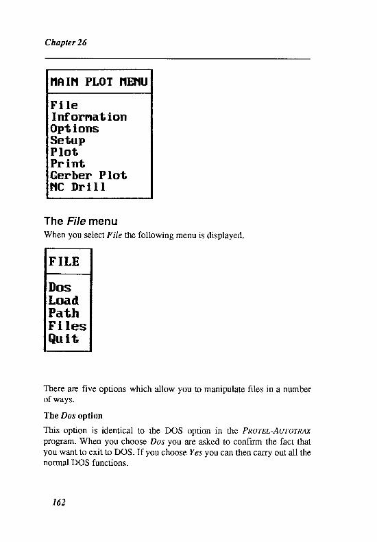
Chapter 26
NRIH PIOT NEHU
F i l eInf ornationOptions$etupPlotPrlntGerber Plotlfc llri I I
The File menuWhen you select File the following menu is displayed.
There are five options which allow you !o manipulate files in a numberof ways.
The Dos option
This option is identical !o the DOS option in the Pnornr-Awornexprogram. When you choose Dos you are asked to confirm the fact thatyou want to exit to DOS. If you choose Yes you can then carry out all thenormal DOS functions.
162
Using the TRAXPLOT Program
The same restrictions as those mentioned in the Pnorgt-Avtornm
program apply.
When you are ready to continue using the TRNQLOT program, simply
type:
EXIT and press (<ENTER>>
at the DOS prompt and you will be returned to the program.
Loading a file
The Load option allows you to load the .PCB file that you want to print
or plot. When you choose the option an input window opens asking you
to enter the name of the file you want to load. Enter the name then press
<ENTER>> or click <LEFT MOUSE>>.
The default value of *.PCB in the window indicates that if you do not
remember the name of the file you can press <ENIER> to call up the
information window which lists the names of all the .PCB files in the
currently selected directory.
When you choose a file and the load begins, a load window will open
showing the items being loaded into memory. This window gives you a
good idea of the number of components and other items that will be
plotted or printed.
When the file has been loaded, the information in the status window is
updated to show the name of the new file.
If there are no files available for printing or plotting, the message:
NO FILES FOUND
is displayed.
Changing the path name
If you choose Path, you can change the path to the directory containing
the .PCB files you want to print or plor
An input window opens asking for the name of ttre new path. Type in the
path name then press <ENTER>> or click <LEFT MOUSE>>.
If ttre path doesn't exist then the elror 'PATH NOT FOUND' is
displayed.
163

Chapter 26
Once you have speciried a path, this will automatically be appended tothe front of any file specification that you enter in the Load option.
Listing frles
When you choose the Files optiotr, I window opens asking you to enter amask for the filenames that you want to list. If you enter:
*.*
then all the files in the currently selected directory are displayed. If youenter something like:
*.PCB
then only the .PCB files are listed.
Quitting
This option allows you to quit the program. Choose Quit and a windowopens asking you to confirm the fact that you want to quit to DOS. If youchoose No then you can continue using the program. If you choose Yesyou are returned to DOS.
Displaying information about the boardIf you choose Infornwtion, a window which displays informationrelating to ttre plot or print is displayed. The information in the windowis shown below.
I]IFORNfiT I
P lot TgpeP lot Sca lePr int Sca le
Ho les in LagoutLouXLot'lIH ishxH ighI
Check P lot1 , B B1 . B B
gBBZ;675z56B
r64
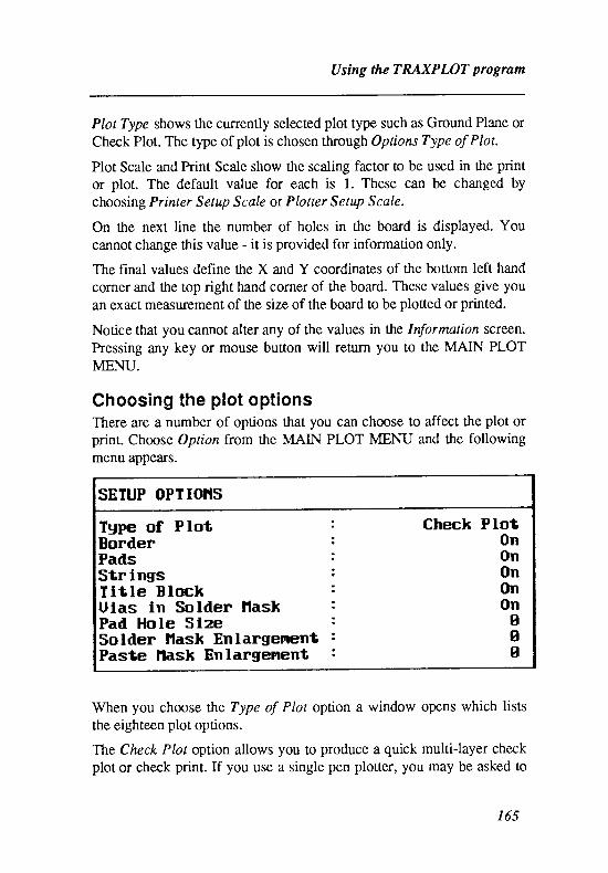
Using the TRAXPLOT program
Plot Type shows the currently selected plot type such as Ground Plane or
Check Plot. The type of plot is chosen through Options Type of Plot.
Plot Scale and Print Scale show the scaling factor to be used in the print
or plot. The default value for each is l. These can be changed bychoosing Printer Setup Scale or Plotter Setup Scale.
On the next line the number of holes in the board is displayed. You
cannot change this value - it is provided for information only.
The final values define ttre X and Y coordinates of the bottom left hand
corner and the top right hand corner of the board. These values give you
an exact measurement of the size of the board to be plotted or printed.
Notice that you cannot alter any of the values in the Information scr@n.
Pressing any key or mouse button will return you to the MAIN PLOT
MENU.
Choosing the plot opt ionsThere are a number of options that you can choose to affect the plot orprint. Choose Option from ttre MAIN PLOT MENU and the followingmenu appears.
When you choose the Type of Plot option a window opens which lists
the eighteen plot options.
The Check PIot option allows you to produce a quick multi-layer checkplot or check print. If you use a single pen plotter, you may be asked to
SETUP OPT IO]IS
Tgpe of P lotBorderPadsStr ingsT it le B lochU ias ln So lder llaskPad Hs le S izeSo lder llask En largenentPaste llask En largenent
Check P lotOnOnOnOnOn
BBB
r6s
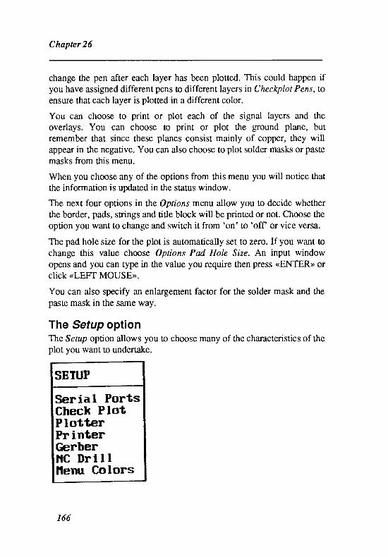
Chapter 26
change the pen after each layer has been plotted. This could happen ifyou have assigned different pens to different layers in Checkplot Pens, toensure that each layer is plotted in a different color.
You can choose to print or plot each of the signal layers and theoverlays. You can choose to print or plot the ground plane, butremember that since these planes consist mainly of copper, they willappear in the negative. You can also choose to plot solder masks or pastemasks from this menu.
When you choose any of the options from this menu you will notice thatthe information is updated in the status window.
The next four options in the Options menu allow you !o decide whetherthe border, pads, strings and title block will be printed or not. Choose theoption you want to change and switch it from 'on' to 'off or vice versa.
The pad hole size for the plot is automatically set to zero. If you want tochange this value choose Options Pad Hole Size. An input windowopens and you can type in the value you require then press <ENTER>> orclick <LEFT MOUSE>>.
You can also specify an enlargement factor for the solder mask and thepaste mask in the same way.
The Setup optionThe Setup option allows you to choose many of the characteristics of theplot you want to undertake.
SETUP
$erial PortsCheck PlotPlotterPrlnterGerberHC llrt I Iilenu Colors
r66
Using the TRAXPLOT program
Serial ports
When you choose Setup Serial Ports a window opens allowing you to
choose one of two serial ports. Choose either port I or port 2, then click<<ENTER>> or press <LEFT MOUSE>>.
You can now change some of the serial port parameters such as the baud
rate, the number of data bits, the parity type and the number of stop bits.
There is a detailed description of these features in Appendix B of this
manual.
Check plot
Choose Setup Clwck Plot to select the layers you want to be output in the
check plot.
A window listing each of the layers opens. You can then toggle each
layer 'on' or 'off' as required.
Plotter setup
When you choose the Plotter option, a window opens allowing you to
change a number of parameters relating !o the plot. If you choose Type a
window will open listing the types of plotter for which drivers ffe
available. Select one by highlighting it then pressing <ENTER> or
clicking <LEFT MOUSE>>.
Choos e Device to select a serial port, parallel port or an output file as the
device to which the output will be sent.
The Scale option lets you enlarge or reduce a plot and to correct for
scaling errors inherent in your plotter.
If you are producing final artwork, you may want the plots to be twice
the size of the normal output. To do this, change the Scale to 2. If you
want to reduce the artwork to half the size, change the Scale factor to
0.5.
The correction values change the scaling in either the X direction or the
Y direction. You may need tn use these correction factors if your plotter
is inaccurate in either the X or Y direction. To check for erors, draw avertical and horizontal track of exactly the same length. When you have
plotted ttre tracks, measure them carefully. If they are not the same you
will need to correct either the X or the Y value.
167
Chapter 26
The X and Y offsets are used to start the plot at a point other than thenormal origin. This may be because you want to plot more than one
board on ttre same piece of film, for example. Enter a new value for boththe X and Y offsets and the press <<ENTER>> or click <LEFT MOUSE>>.
Choose Orientation trl select 'Normal' or 'Rotated' for the final plot.
Choose Qualiry tll select 'Draft' or 'Final Artwork' for the plot.
If you choose Setup Pens a window opens which allows you to changepen parameters. The Check Plot Pens option allows you to specify a pen
number for each of the check plot layers. Note that more than one layercan have the same pen number. You can also specify the number for themain pen and the speed which the pens lravel. The figure is given in milsper second and the default speed is 5000. You can also change the sizeof each of the eight pens.
Frinter setup
The procedure for setting up a printer is similar to the procedure forsetting up a plotter.
The Orientation option has the extra option of Auto Centre. Thisprovides for a print to be centered on the printer paper. Note that thisoption will override any offsets which have been set up.
Another variation is that you can choose between continuous paper andsingle sheet paper.
You may have to use the Scale option if you are using a printer withslightly different characteristics to the Epson FX series.
The Epson FX series has a vertical slep size of U72 inch. The Epson LQseries, however, has a vertical step size of UA inch. This means that720 dots is 10 inches long on an FX series printerand 12 inches long onan LQ series printer. The oulput will therefore be longer in the Xdirection on an LQ series printer. To make it the same the dislance in theX direction must be reduced by a factor of I .2. Therefore you will needto make the X-correction factor 0.833.
168
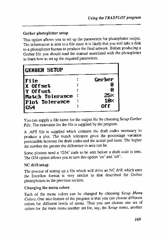
Using the TRAXPLOT Program
Gerber photoPlotter setuP
This option allows you to set up the parameters for photoplotter output.
The information is senr to a file since it is likely that you will take a disk
to a phot,oplotter bureau to produce the final artwork. Before producing a
Gerter file you should read the manual associated with the photoplotter
to learn how to Set up the required parameters.
GERBER SETUP
F i l eX OffsetU Offsetlfatch TolerancePlot TolerantreG54
GerberBB
?:5nLEn
off
you can supply a file name for the output fite by choosing Setup Gerber
File. The extension for ttre file is supplied by the program.
A .ApT file is supplied which contains the draft codes necessary to
produce a plor fne match tolerance gives the percentage variation
permissible between the draft codes and the acnral pad sizes. The higher
the number the greater the difference in area can be.
some plotters need a 'G54'� code to be sent before a draft code is sent.
The G54 option allows you to turn this option 'on' and 'off'.
NC drill setuP
The process of setring up a file which will drive an NC drill which uses
the Excellon format is very similar to that described for Gerber
photoplotters in the previous section.
Changing the menu colors
Each of the menu colors can be changed by choosing Setup Menu
Colors. One nice feature of the program is that you can choose different
colors for different levels of menu. Thus you can choose one set of
colors for the main menu another set for, say, the Se tup menu' another
169

Chapter 26
for the Plotter Setup menu and another for the Printer Device menu.
Notice that after setting up the menu colors for the first level, you cancopy the previous setup down to the next level of menu.
Printing or plott ing a pCBThe final action you need to take is the actual print or plot. Make surethat your printer or plotter is turned on and is online. Choo se Plot fromthe MAIN MENU after making sure that all the Setup options are correctand that you have loaded a file. You can check all this in the statuswindow.
The program will check the file and assemble the information relating tothe layer or layers to be output. The information window will keep youinformed of the progress of the plot.
If the output does not appear within a few minutes, check ttrat ttre printeris online and plugged into the correct port.
A similar process occurs if you choose Print, Gerber Plot or NC Drillfrom the MAIN PLOT MENU. Remember that the last two optionsalways produce plot files.
170
27 rHE "??ffi#otlg PLIBSIaNt : :
program Disk A contains nvo utilities which allow you to convert files
created with pnornt-Pc|.3.0 so that they are compatible with Pnorst-
AurorRN{.
The PCBSCON ProgramThis program will convert PCB files created with Pnornt-PCB 3.0 so
that they can be loaded into PvOrAu-AUTOTRN(.
The simplest way to convert a file called, say, BOARD.PCB is to return
to the DOS Prompt and tYPe:
PCB3CON B OARD.PCB NEWB OARD.PCB
Thus, the name of the Pn orrt-AwoTR$( file is now NEWBOARD.PCB.
If you do not specify the .PCB extension, that extsnsion will be forced
by the program.
If you just type:
PCB3CON and Press <<ENTER>>
then you will be prompted to supply the old file name and the new file
nalTlg.
The program also asks you whether you want the component designator
text and comment text hidden and which pad shape you wanl
Remember that ttre progam is stored on Program Disk A, so you have to
make sure that this disk and the disk containing the files are present if
you have a dual-floppy drive system.
you can specify complete path names for both ttre old file and the new
file.
17I

Chapter 27
The PLIB7CON programThis program has exactly the same structure as the PCB3CON program.It is used to convert libraries that you might have created with PnornuPCB -3.0 so that they are compatible with pnoru,AworR*L
If you want to convert a library called OLDLIB.LIB to be calledNEWLIB.LIB then rype:
PLIB3CON OLDLIB.LIB I{EWLIB.LIB
All the other features of the program are the same as for PCB3CONexcept that you are only prompted to supply the pad shape.
You need to be aware that libraries created with Pnornt-PCB 3.0 mayincrease in size significantly when converted. The reason is that there ismore information stored about each pad rn Pnorru-AworR*( libraries.
172

APPENDICES

A FEATURES OF PROTEL-AUTOTRAX
This appendix outlines the technical features of Pnorrt-Awornmwhich you may need to refer to from time to time.
lmportant fi lesThe files that are supplied with the package are:
TRAXEDIT.EXE This is one of the main program ftles. It must be
tr*ilrr.Bi^lame directory as the rile
Ihe file is supplied on Program Disk A.
TRAXEDIT.OVR This is the 'overlay' part of the program. While
this is part of the main pro$am it resides on the
1[l;$#*ff#ry#n"'��TRAXEDIT.EXE file.
If you have EMS memory installed, the .OVR
file is loaded into that portion of memory, thus
making calls to the overlay very fast.
The file is supplied on Program Disk B.
TRAXSTD.LIB This is the main library file which contains the
patterns for the components you are likely toplace on your boards. Note that SMD devices are
included in this library.
This file is supplied on the Library Disk.
175

Appendix A
TRAXEDIT.PAD
TRA)(EDIT.MNU
TRAXEDIT.KEY
DEMO.PCB
PLACED.PCB
DEMO.NET
EGA.BAT
CGA.BAT
This file contains information about the defaultpad fi)es. This is the file that is loaded when theprogram starts. It must be stored in the currentlyselected directory or a directory pointed to by theDOS Path command.
This file is supplied on Pro$am Disk A.
This file holds the menu messages and the errormessages used by Pnorg,t-Atnornur and mustalways be available to the program at start up.
The file is supplied on Program Disk A.
This file holds the default key macros which areautomatically loaded when you start Pnorm-AL]T}TRN{.
The file is supplied on Progam Disk A.
This is one of the demonstration PCB files whichis referred to in the manual. All PCB filesgenerated with the Pnorrt-Awornex programhave a .PCB extension. This board has alreadybeen routed.
This file is supplied on the Library Disk.
This is the unrouted version of DEMO.PCB.
This file is supplied on the Library Disk.
This is the netlist file with the information whichis used to route the PLACED.PCB board.
This file is supplied on the Library Disk.
A batch file which you can r:se to ensure that theprogram uses an EGA gra'pnics driver.
A batch file which you can use to ensure that theprogram uses a CGA graphics driver.
176
F eatures of P norEL'AworRAx
The files that you might create have the following extensions:
HERC.BAT
VEGA.BAT
VGA.BAT
GRAPH.DRV
.PCB
.NET
.PAD
.KEY
Files that might beprogam are:
???.BAK
???.ABK
A batch file which you can use to ensure that the
program uses a He,rcules graphics driver.
A batch file which you can use to ensure that the
program uses a vega Deluxe graphics driver.
A batch file which you can use to ensure that the
program uses a VGA graphics driver.
The currently selected graphics driver.
This extension will be attached to any PCB files
that you create.
This extension is attached to the netlist files you
create with the Highlight Make Netlist option in
PnOff,t-AtnOfn*for those that you have created
with the Pn InEL-S;HEMATIC ptogram.
These are the files containing the pad types
which you have defined.
These are the files you have created which
conlain the keyboard macros that you have
defined.
created while you are using the PnOftt-AWOrnUr
This file is created when you save a PCB file. It
is a copy of the previous save of the file. If you
realise that you have made a major error in the
cturent editing session, you can restore your file
to its previous state by renaming the .BAK file.
This is the file which is automatically created
every 30 minutes (or whatever you have set the
backup time t0 be in the Current Backup op1on).
If your system crashes and you need to restore
your file from the latest backup, simply rename
this file with the name of your cunent .PCB file.
177
Appendix A
Hardware and software check listIn order to use the Pnorm-Artrornur software you will need thefollowing:
An IBM-PC microcomputer or compatible
2 disk drives (2 floppy drives or one floppy drive and onehard drive) - a hard drive is recommended
Graphics card (CGA, EGA, Hercules, VGA or VegaDeluxe)
Colour monitor
One parallel printer port
Microsoft mouse or compatible (recommended)
Draft printer
MS-DOS or PC-DOS (Version 2.0 or grearer)
You will need access to:
A pen and ink plotter
A G erber-compatible photoplotter
An Excellon format N/C drill
Hardware requirementsTo use the Pnorrt-Atnornur software you will need an IBM-PCAryAT or IBM PSl2 microcompurer (or compatible).
The microcomputer should have at least 640K RAM and the softwarewill support expanded memory boards which conform to the L.f.M.standard.
The software will perform adequately on a machine with an 8088microprocessor running at 4.77 MHz, but you will notice a significantincrease in speed if a higher clock speed or a more advanced processor(such as an 80286 or 80386) is used.
Installing a numeric coprocessor will not lead to an increase in speedsince the Pn ornt-AworR*( software only uses integer calculations.
I7g

F eatures of P norEL-AworRAx
The system should have at least two floppy disk drives or one floppy
disk and one hard disk drive. A single drive system is not suitable.
A range of colour cards is supported. The software will work with a
Colour Graphics Adaptor (CGA) card, an Enhanced Graphics Adaptor
(EGA) card, Hercules card, VGA card and the Vega Deluxe card.
Monochrome cards are not supported.
The higher resolution of the EGA, VGA and Vega Deluxe cards make
them preferable for intricate design work, however many users have
achieved excellenl results with CGA systems.
New drivers will be added to this set in the future.
A colour monitor which suits the graphics card is required.
While the software has been designed to work with keyboard-only
systems it is strongly recommended that either a serial mouse or a bus
mouse be installed. The software works with the Microsoft Mouse or any
mouse that is 100% compatible with it.
A dot matrix printer is recommended for draft prints. The software
supports the Epson FX and LQ series and the HP Laserjet II-
pnornt-Avrornur supports the popular I{P-GL, DM-PL, and Roland
DXY 800 plotter languages. There are numerous plotters available which
support these plotting languages, and they span wide price/performance
tanges. The following plotters are just a few which have been used
successfully by P nOTEL-AUTOTRN{ customers.
Iry.-7440A (ColourPro), 7475A, 7550A, 7570A. (DraftPro),
75808, 75858, 75868 series.
Houston Instruments DMP-40, 4 1142, 5U52, 56 series.
Roland DXT 800, DXY 880, 980 series.
Enter Computer Sweet-P Plotters.
Protel PT10l Bench Top Photoplotter
The pnornr-Awornex software supports Gerber photoplotters and
photoplotters that emulate the Gerber series. These photoplotters
179
Appendix A
produce high quality PCB artwork and are accurate to the Pnornt-Aurornur I mil resolution.
The software also produces N/C drill files conforming to the Excellonformat, including automatic drill changes.
Software requirementsIn addition to the Pnorat-Awornax software you will need a copy ofeither ttre MS-DOS or PC-DOS operating system. The version numbershould b,2.0 or greater.
The Pnornt-Awornex software provides automatic backups of yourfiles, but it is strongly recommended that a regular backup of .PCB filesis made onto a different disk.
You should use ttre DOS COPY command to copy your .PCB files to adifferenl disk, then store that disk in a different location. It is also a goodidea to back up your .KEY, .LIB and .PAD files from time to time aswell.
Pnoret-AurorRAx check I istWhen you receive your Pnorrt-Avrornil( package you should find thefollowing contents:
The P nornt-Atnornur reference manual
Four disks labelled Program Disk A, Program Disk B,Library Disk and Plot Disk - which contain ttre Pn orEL-Aurornm programs and ttre associated files.
The external protection device, which plugs into theparallel printer port of your microcomputer and allows thePnornt-Atnornur program to work.
The Software License Agreement Form, which you shouldfill out and return immediately. This is vital if you requirefurther support or information about future updates andrevisions.
r80
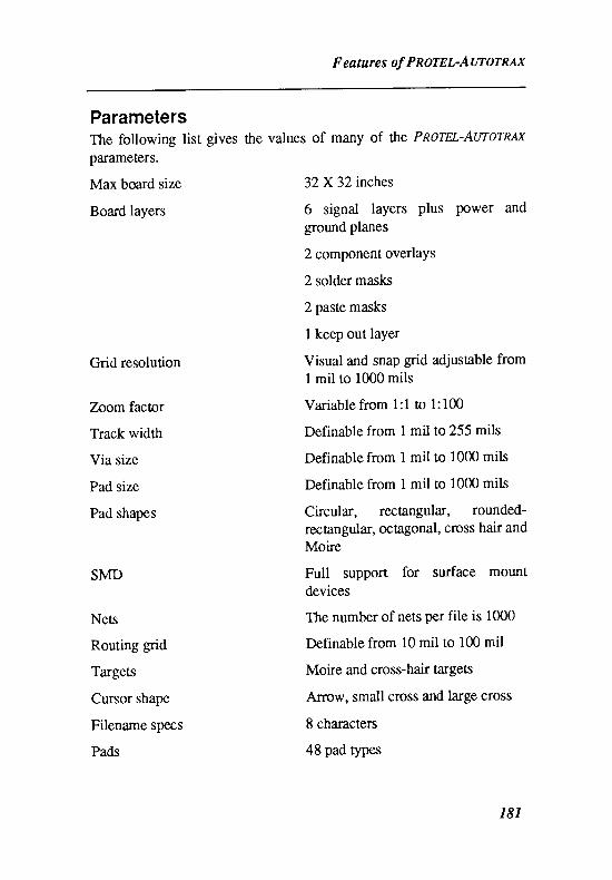
F eatures of P norEL-AworRAX
ParametersThe following list gives the values of many of the Pnornt-Avrorn$r
parameters.
Max board size 32X 32 inches
Board layers 6 signal layers plus power andground planes
2 component overlays
2 solder masks
2 paste masks
I keep out layer
Grid resolurion Visual and snap grid adjustable from
I mil to 1000 mils
Zrrom factor Variable from 1:1 to 1: 100
Track width Definable from I mil to 255 mils
Via size Definable from I mil to 1000 mils
Pad size Definable from 1 mil to 1000 mils
Pad shapes Circular, fstangular, founded-rectangular, octagonal, cross hair andMoire
SMD Full support for surface mount
devices
Nets The number of nets per file is 1000
Routing gnd Definable from l0 mil to 100 mil
Targets Moire and cross-hair targets
Cursor shape Arrow, small cross and large cross
Filename specs 8 characters
Pads 48 pad types
181

Appendix A
Key macros 48 key macros
Library components 200 components maximum in anyone library
Max string size 1000 mils
Min string size 36 mils
182
B Rs2 g2-ccoNstDERATtoNs
Many plotters come equipped with a RS232-C interface, and a cable is
required between the plotter and computer to provide data transmission
and handshaking. Correctly configuring this cable can be an exasperating
task even for experienced engineers. This appendix explains the
relevant RS232-C conventions, and gives wiring diagrams for cables that
have been tested on a wide variety of plotters and computers with lA07o
success.
It is natural to ask why parallel interfaces seem to work every time with
no problems, whereas serial interfaces can take great amounts of time
and patience t0 set up.
Serial versus parallel interfacesParatlel interfaces provide one-way Eansmission only, from a computer
to a peripheral device, such as a printer or a plouer. Since data is only
transmitted in one direction, the data and handshaking connections and
their direction of flow are straight-forward. All data bits (8) originate
from the computer and are received by the peripheral. The data strobe
signal obviousty originates at the computer as well, since it indicates that
valid data is on the bus. The acknowledge and busy lines clearly
originate from the peripheral, and so on with all of ttre signals. A
standard cable has been defined for all these signals, atrd the computer
and peripheral are intrinsically configured to originate or receive these
signals as appropriate.
However, the RS232-C standard defines the signals for bidirectional
communication between two pieces of equipment, known as Data
Terminal Equipment (DTE). A DTE is defined as:
1. The point of origin for any data to be transmitted, and
2. the final destination for transmitted data.
183
Appendix B
Thus, the computer and plotter are both defined as DTE. This is whereproblems begin. From an RS232-C point of view, both the computer andthe plotter look the same, and signals such as Transmitted Data (from theDTE) are assigned to the same pins in both devices. Contrast this withthe parallel interface in which the interpretation of a signal pin isintrinsic to whether the device originates data or receives it.
Thus, interfacing two DTEs needs an intermediary device or devices toconnect the transmitted data pin of one DTE to the received data pin ofthe other, and vice versa, and to also correctly configure the handshakingsignals. The RS232-C protocol detines Data CommunicationsEquipment (DCE), which connects directly to DCE and transmits andreceives the data over a channel - a DCE does not originate data, nor is itthe final resting place for data. A modem is a DCE that modulates thedata for transmission over a voice channel (a telephone line) anddemodulates it at the receiving end back to digital data.
Cable connectionsIn the case of connecting a computer to a nearby peripheral such as aplotter, the cable is configured to take the place of the DCE connectingtwo DTEs. Because it replaces the modems described previously, such acable is known as a Null Modem. Figure B- I (at the end of this chapter)shows the cable configuration required between an IBM-PC/XT (orcompatible) and a plotter; Figure B-2 shows the cable required betweenthe IBM-AT (or compatible) and a plotter. The IBM-AT uses a DB9connector for its serial port, whereas the other machines use the familiarDB25 connector.
Refer to Figure B-1. Note how the cable connects the Transmitted Data(TXD) of one DTE to the Received Data (RXD) of the other and viceversa, to provide the correct flow of data. The handshaking of the plotteris as follows. When the plotter is ready to receive data it asserts the DataTerminal Ready (DTR) signal. This is received at the computer as ClearTo Send (CTS) and the computer commences transmission. When ttreplotter buffer is full, the DTR line goes low, and the computer sees thatit is no longer clear to send data. As the plotter continues plotting andempties the buffer, its DTR signal again goes high and the computerrecommences data transmission.
184
RS2 32 -C c o nsideratio ns
From the computer's point of view, it requires that CTS is high as well
as Data set Ready (DsR), Data carrier Detect (DcD), and (in some
computers) Ring indicator (RI), before it will transmit data. When the
computer is turned otr, its serial port is initialised and its DTR is
asseited, since the computer (DTE) is now ready. By connecting the
computer DTR, DsR, DcD, and RI lines within the shell of the
connector, the computer can sense that a valid connector is plugged into
its serial port.
The cable is then made symmetrical so that either end of the cable can be
plugged into the computer or plotter. (Jsers of Houston Instruments
DMp plotters will find this handy, since the plotter uses the same male
DB25 connector as the IBM-PCIKT. With I{P plotters this symmetry
isn,t as important, since the FIP plotters use female DB25 connectors and
the cable ends cannot be swapped. Use the correct connectors to plug
into your plotter and computer, and follow the connections outlined in
Figure B- I "
If you are using the IBM-AT (or compatible) computer, either obtain a
DB9 to DB25 adapter and use the cable of Figure B-1, or use the cable
of Figure B-zto connect directly to the DB9 connector on the computer.
This discussion should allow you to connect your computer and plotter
without problems, and should enable you to interface with other serial
devices as well. Refer to the manual that comes with your plotter for
further information on its interfacing and handshaking. The cable given
in this appendix may differ slightly from the one given in your plotter
manual, but it should be rried inidally. It conforms strictly to RS232-C
definitions and has been made generally to suit the widest variety of
peripherals and compatible computers possible.
Baud rate, data bits, etc-The other important consideration when using a serial interface is to
match the baud rate (110-9600), the number of data bits (7 or 8)' stop
bits (l or 2) nd the parity bit (Odd, Even, or None) of both the computer
and plotter. yo* plotter manual should indicate ttre default settings of
the plotter upon being powered up, and will contain information on
changlng the communications setup. Some ploners do not have default
settings but have DIP swirch settings for the communication parameters.
r85
Apryndix B
Set up your plotter according to the manual and then be sure to matchthese settings with those in the Traxplor program. These settings arestored when the plot finishes, so that once they are set correctly they willnot have !o be changed while using the same plotter.
For those of you with no idea of how you should initially set yourplotter, use the following values to begin with:
Baud Rate: 24m
Data Bits: 8
Stop Bits: z
Parity: N
This is an intermediate baud rate and will yield error-free datatransmission for reasonably long cables.
What to do in case of problems1. Don't panic! First check your cable connections, make sure no
wires have broken, and check that your Traxplor settingmatches the baud rate, parity, etc. of your plotter.
2. Make sure you are using the correct serial port. If Traxplotspecified serial port I (COMI:), make sure your plotter isconnected to that port and not the parallel port or another serialport.
3. If your plot goes all right for a while and then starts puttingstray lines and arcs all over the layout, this generally indicatesimproper handshaking. Check that your cable is configuredexactly as in the appropriate diagram, ond check that allcommunications settings match. This problem can also occur ifthe data is being corrupted. Keep ttre plotter cable as short aspossible and keep it away from power cords, etc. If you areusing a long cable, you may have to reduce the baud rate toobtain error-free transmission. Due to the disributed resistanceand capacitance of cables, there is a trade-off between cablelength and baud rate for reliable data transmission.
186
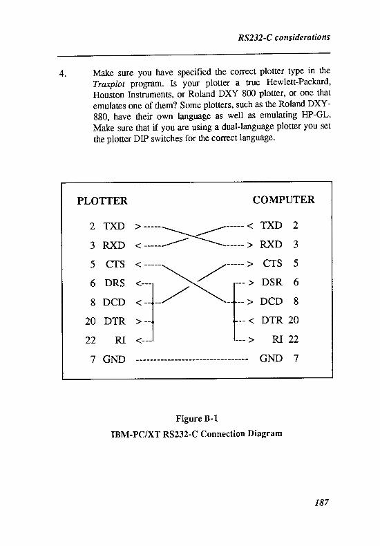
RS2 32 -C c onsiderations
4. Make sure you have specified the correct plotter type in the
Traxplot program. Is your plotter a true Hewlett-Packard,
Houston Instruments, or Roland DXY 800 plotter, of one that
emulates one of them? Some plotters, such as the Roland DXY-
880, have their own language as well as emulating I{P-GL.
Make sure that if you are using a dual-language plotter you set
the plotter DIP switches for the correct language.
Figure B-1
IBM-PC/XT RS232-C Connection Diagram
PLOTTER
2 TXD
3 RXD
5 CTS
6 DRS
8 DCD
20 DTR
2 2 z u
7 GND
UTER
2
3
5
6
8
20
22
7
187
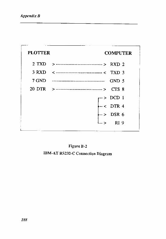
Appendix B
PLOTTER
2 TXD
3 RXD
7 GND
20 DTR
COMPUTER
RXD 2
TXD 3
GND 5
CTS 8
DCD 1
DTR 4
DSR 6
z u 9
F:[ :
Figure R-2
IBM-AT RS232-C Connection Diagram
r88
C ERROR MESSAGES
This appendix provides a brief explanation of each of the elror messages
which occur while using ttre Pnorst-Atnornur and TRilQLOT
programs. They are arranged in alphabetical order of the fint character
in the message to make them ulsy to look up.
Non-fatal errorsBAD FORMAT IN KEY MACRO FILE
The key macro file which has an extension of .KEY has
been c,orrupted. This may have occurred during editing
with a word processor.
To overcome the problem, delets the key macro file and
copy the backup key macro file into that directory. This
remedy assumes that you have made regular backups ofyour important files.
BAD FORMAT IN PAD TYPE FTLE
The pad type file which has an extension of .PAD has
been colrupted.
The remedy is the same as for the key macro file.
BAD LIBRARY FILE FORMAT
The library tile which has an extension of .LIB has been
corTupted.
The remedy is the same as that for the key macro and pad
type files.
189
Appendix C
BAD PCB FILE FORMAT
The PCB file with an extension of .PCB has been
corrupted.
The remedy is to delete the file and ttren copy the latest
backup into the directory, or to rename the automatic
backup file which is created every 30 minutes under the
.ABK extension.
BLOCKNOTMARKED
You have attempted to move, copy or delete a blockwithout rirst defining a block.
Choose Block Define to define the block and then carry
out the required operation.
COMPONENT DESIGNATOR IS ALREADY USED
You have attempted to assign a component designator that
has already been used for another component on the
board.
When you place a component the program will
automatically supply the next available designator if you
type, sy, U? instead of, say, U3. If you are placing a
number of components of the same type the designatorwhich appears in the input window will automatically be
the next available.
COMPONENT NOT FOUND
This elror will occur if you attempt a Jwnp Component
operation to a non-existent component.
Choose Information Components to check which
components are curently placed.
COMPONENT NOT FOUND IN LIBRARY
If you are placing a component or renaming a componentand you enter a component name which does not exist in
the component library then this error message will appear.
190
Error messages
It is possible that you may not have specified the name
correctly. To rectify the problem enter a <<?>> and press<<ENTER>> or click <LEFT MOUSE>>. Then select the
component you require from the list provided. If the
component name does not appear in the list you may need
to select another library.
CURRENTLAYER MUST BE TURNED ON
You have attempted to turn a layer 'off (in Serup Toggle
Layer) when it is the currently selected layer.
To overcome the problem exit from this menu and select
another layer to be the current layer, then try again.
FILE NOTFOUND
You have attempted to load a file which is not in the
curently selected directory. This may occur if you do not
specify the name of the file correctly.
To overcome the problem, check the name of the file with
File Files or change the path with File Path.
KEY MACROFILE NOTFOUND
You have specified a key macro file which does not exist.
Choose File Files and enter the mask *.KEY, then inspect
the names of the key macro files on your disk.
KEY MACRO KEY ALREADY USED
You have attempted to assign a key macro to a function
key which already has one assigned to it. This may occurin Setup Keys Assign or Setup Keys New.
If you still want to assign the macro to that key you must
first clear the key by choosing Setup Keys Delete.
KEY MACRONAME ALREADY USED
You have attempted to assign a name to a key macrowhich is already in use. This may occur in Setup KeysRename or Setup Keys New.
To overcome the problem simply enter a different name.
r91
Appendix C
KEY MACRONOTFOUND
You have specified a key macro which does not exist.
LIBRARY FILE ALREADY EXISTS
This error will occur if you choose Library'lr{ew Libraryand try to specify a name for the new library whichalready exists.
To overcome ttre problem, change the name you want tngive to the new library.
LIBRARY FILE NOT FOUND
You have ried to load a library which has either not yet
been created or is not, in the directory specified.
LIBRARY FULL
You have attempted to add a component to a library whichalready has 2W components in it.
To overcome ttre problem either delete a component fromthe library first, or create a new library.
LIBRARY NAME IS ALREADY USED
This error occurs during the Library Add option if you tryto add a new component to a library and assign a namewhich already exists.
Check the names of the components in the library withLibrary List and then change the name of the newcomponent so that it does not clash with an existing name.
NETNAMENOTFOUND
You might have chosen Jump Net and specified a netname which does not exist.
Check that you have supplied the correct net name or thatyou have loaded the correct netlist using Netlist Get Nets.
NETLIST FILE NOT FOT]ND
You have attempted to load a netlist file in Netlist GetNets which could not be found.
192
Enor messages
Check the names of the files on the disk. Also check Filepathto make sure that the correct path has been specified.
If you are using a floppy disk system make sure that the
correct drive has been selected and that you have inserted
the correct disk.
NO COMPONENTS IN LIBRARY
you have just created a new library file and then tried to
Library List, Library Browse or Place Component or a
similar option.
you wilt need to add some components to the current
library or change to a different library.
NO COMPONENTS PLACED
you have attempted to select a component when there are
no components Placed on the board.
NO KEY MACROS LOADED
An attempt has been made to refer to a key macro when
no macros have been loaded. Key macros are stored in a
file called PCBEDIT.KEY. This file is automatically
loaded when you start the PCBEDIT program.
This elror will occur when you try t0 carry out many of
the functions in Setup Keys if you have cleared the key
macros from the memory.
To overcome the problem, choose Setup Keys Load and
load in a key macro file.
NO LIBRARY HAS BEEN OPENED
You have tried to load a component or save a componenf
without first having specified a library.
Normally, the default tibrary is opened when you start
Pnorg,t-AWornex. If no library is open check your disk
or directory to make sure a library tile exists.
r93
Appendix C
NO NETS LOADED
You have attempted to carry out a netlist operation such asNetlist Optimize or Netlist List when there are no netscurrently in the memory.
You will need to load some nets from a .NET rile by usingNetlist Get Nets.
NO OUTLINE ON KEEPOI,N LAYER
You have attempted to place components automaticallyusing Netlist Awo Place without having specified theoutline of the board on the keep out layer.
Use Place Track to put an outline on the keep out layer.
NO PAD TYPES LOADED
The .PAD file should be loaded automatically when youstart P nornt-Atnornur.
Make sure the .PAD file is on the correct floppy disk or isin the correct directory.
NO PINS HAVE BEEN HIGHLIGHTED
You have chosen the Information Highlighted Pins optionwittrout having firsr highlighted any pins.
To rectify the problem choose Highlight Net or HighlightConnection and highlight some pins.
NOPINS ONTHATPLANE
You have tried to list the nets on the power or groundplane when no connections have been made.
Check that you really want the connections to be on thatplane. If you do, then turn that plane on with Setup ToggleLayers and make the required connections.
NO PRIMITIVES FOR LIBRARY COMPONENT
You have tried tro save a component to a library but havenot yet defined any primitives such as pads or tracks forthat component.
194
Error messages
NOT ENOUGH MEMORY FOR COMPONENT
You have tried to create a componenl or merge a
component when there is not enough memory available.
If you need the new component then delete one of the
existing components before loading the new one.
NOTENOUGHMEMORYTO SUSPEND TO DOS
There is not enough memory left to exit t0 Dos.
you should either choose Fite Quit or continue working
without exiting t0 Dos.
ONLY 48 KEY MACROS AT AI'IY TIME
An attempt has been made to define a 49th key macro.
Pnors,t-AWornryr only allows 48 key macros to be
defined at any time.
To overcome the problem choose Setup Keys Delete and
delete a macro you no longer need before defining the new
macro.
ONLY 48 PAD TYPES AT AI{Y TIME
You have attempted to define a new pad type and 48 have
already been defined. A ma.:timum of 48 pad types is
allowed in the Pnorg,r-ArttornAx program.
If you decide tfiat you need the new pad type you must
frst delete one of the existing types or change one of the
existing types using the Edit Pad option.
OUTOFMEMORY
There is not enough memory for the operation you have
attempted.
This is likely to happen if you attempt t11 load a large
.PCB file.
PADNOTFOUND
you have chosen the Jtunp Pad option and specified a pad
number which does not exist on the chosen component.
195
Appendix C
An example would be selecting a DIP16 pattern and thenspecifying pin 17 for the jump.
Check the number of pins in the component and specify apin which exists.
PAD TYPE FILE NOTFOUND
The pad type definitions are stored in a file with a .PADextension. This file must be in the same directory as ttre.EXE file.
Check that the file has not been deleted or moved to adifferent directory.
PAD ryPE NAME ALREADY USED
You have attempted to give a name to a new pad whenthat name is already in use.
Either change the name of the new pad or use Edit Pad tochange the name of the existing pad.
PAD ryPENOTFOUND
You have tried to select a pad type which does not exist.
PATHNOTFOUND
You have attempted to specify a non-existent drive ordirectory in the File Path option.
Check the path specification to ensure that both the driveand the directory actually exist.
PCB FILE NOT FOUND
An attempt has been made rn FiIe Load to load a PCB filewhich does not exist or which cannot be found.
Check the names of the PCB files with the File Filesoption. If the filename is not displayed, then check FilePath to see if the correct pathname has been specified. Ifyou are using a floppy disk system, check to see that thecolrect drive is specified and that the right disk has beeninserted.
196
Error messages
SMD PADS ON OUTSIDE LAYERS ONLY
You have tried !o place a Surface Mount Device (SMD)
on an inside layer of the board.
An SMD can only be assigned to either the top layer or the
bottom layer and belongs to only one of those layers.
STRING NOTFOUND
You have specified a string in the Jump String option
which is not on the board.
This may be because the string you specified is not present
or because you have specified it incorrectly or
incompletely.
Fatal errorsIn each case, these errors cause the program to stop operating. You will
need to start the progrcm again and retrieve the latest version of your
.PCB file from the backup version.
If you generate a fatal error and cannot work out the reason for it, we
would appreciate it if you contacted hotel Technology Pty Ltd.
Division By kro Error. TRAXEDIT Program Aborted.
The program has attempted to carry out a fatal division by
zeto operation. Dos traps such an error and causes the
program to stop operating.
Stack Overflow Enor. TRA)(EDIT hogram Aborted.
The stack has overflowed for some reason. This is a rare
eITOr.
Not Enough Memory. TRAXEDIT Program Aborted.
You have run out of memofY, possibly because your PCB
file has become loo large.
Floating Point Overflow Error. TRAXEDIT Program Aborted.
Another rare elTor over which you have no control.
197

Appendix C
Floating Point Underflow Error. TRAXEDIT Program Aborted.
Same as for Overflow error
Not Enough Memory To Start TRAXEDIT.
This suggests that one or more resident progfams are
already in the memory. You are likely to generate this
error if you suspend to Dos by choosing File Dos and then
try to start the progam by typing TRAIGDIT instead ofEXIT.
TRA)GDIT.MNU Not Found. TRAXEDIT Program Aborted.
All of the menu descriptions and messages are held in afile called TRAXEDIT.MNU. This file must be in the
currently selected directory when the program is started.
Security Device Not Found, Program Aborted
You have attempted to run the Pnorrt-AworRu{ program
without having fint connected the external security devicesupplied with the program.
r98
D A NorE To EDucAToRs
If you are introducing computer-based printed circuit board design to
students then there are a number of factors which you might want to take
into consideration.
Wirh packages of the sophistication of Pnornt-AworRil( within the
price range of most PCB designers, there seems little point in spending
too long teaching students about the raditional methods of designing
boards.
There 8ro, however, some very gmd reasons why students should be
familiar with the basic concepts of printed circuit boards before they
begin designing them on the computer.
Concepts such as layers, tracks, pads, vias and components should be
thoroughly understood before the students attempt to design their own
board using the Pn ortr-AworRil( software.
These concepts can best be understood by being involved in the
production of a simple printed circuit board. Students need to be able to
see a board and be able to understand how the components are connected
and why the tracks are laid the way they are. They need to see the pads
and vias and how ttrey relate to the tracks and components.
Before the students design their own boards, they need to become
familiar with the software. It is assumed that they have already learned
how to use the keyboard and are familiar at an elemen@ level with the
basic DOS commands. They can learn much by using the demonstration
boards and netlist, supplied with the package.
The first set of skills to acquire could be:
starting the Pn orEL-AworRA){ program;
loading the DEMO file;
using the drop-down menus;
selecting with the selection bar and with keystrokes;
r99
Appendix D
using the cursor keys or mouse to move around the board;
speeding up cursor movement with the <SHIFTT kty;
seeking information about the board from the Current,Information, Edit and Setup menus;
locating components, tracks, vias and pads;
changing some of the Serup options;
inspecting the library components with Library Browsei
saving the current board;
quitting from the program.
Notice that all of these skills can be acquired before any design work iscarried out. The students can also become familiar with the TRilGLOTprogram at this stage. They can learn the following skills:
loading the TRHffLOT program;
loading the file t0 be output;
choosing the correct port for ttre printer;
choosing the correct printer;
choosing the setup options for the oulputl
producing the draft outpul
Once these basic skills have been acquired, the students can then moveto the computer-based design stage. Tutorial two and tutorial threecontain much of the basic information required for the design stage.
It is important to inroduce the students to the concepts of netlists andautomatic placement and automatic routing early as these features ofPnornr-Atnorn,ur are not only very powerful, but also make the wholedesign process easier for students to understand.
200

il\DEX


INDE}.
* key 31, 38
+ key 32
- key 32
Absolute cursor mode 69
Absolute origin 69-70
Adding a comPonent to the library
48, 108
Alt key 22,142
Any node routes 123
Arcs, deleting 73-4
Arcs, moving 109-10
Arcs, placing 47 ,I3l-2
Arrow keys 22
Assigning comments 35, 133, 140
Assigning comPment designatoni 35,
1 3 3 , 1 4 0
Assigning key macros 142-3
Auto pan option 146,155
Auto Place 78-9, 116
Automatic backuPs 14,146, 177
Automatic component placement 78-
9 , 1 1 6
Automatic via Placernent 129, 148
Backing up files 14,146,177
Backspace keY ?2
Block menu oPtions 63-8
Blocks, copyrng 67
Blocks, defining 63-4
Blocks, hiding &
Blocks, moving 64-8
Blocks, reading 68
Blocks, saving 68
Board dimensiqrs 95-6
Board status 97 -8
Bottqn layer 151
Bottun overlaY 152
Breaking a track 110
Browsing in the library 103-4
C routes 123
CGA graphics driver 16, 141
Changing 'default' setuP oPtions
r39-52
Changing laYers 3l-2,38, 70
Changing the menu window colour
30-1 , 141
Changing the current Pad tYPe 7O-l
Changing the cursor tYPe 147
Changing the drag oPion L47
Changing the grid size 89-90
Changing the laYer colon 140-1
Changing name of the autornatic
203

Index
backup file 146 componenrs, editing 77 -g
Changing the redraw quality 150 Cunponents, free to move 78
Changing the time between automatic Conponents, jumping to 99-100
backups 16 Cunponenrs, listing in library 96-7
Changing track widths 71, 80, 125 Cunponenrs, lisring those placed on
Checking the pins in a net 96 the board 96
Checking the pins on a component Cunponents, locked 78-9, 116
37,lol Conponents, moving I lo
Chevrons < >> 2l Cunponents, placing l3Z-3
choosing a component from the camponents, placing automaticallylibrary 34-5, 103 7g-9, I 16
Choosing a different library lffi-7 Curnectio's, highlighting gl_z
Choosing options frqn menus 24,32 Co,nnections, length l 19
Clearing a file 34, 83 Contracting the display 31, 156
clearing a netlist ll7 converting Prorel-pcB 3.0 files l7l
clearing key macros 53,143 converring protel-pcB library 3.0
Clearing the work space 34, 83 files l7Z
Colors, layers 140-l Copying a block 67
Colors, menu window l4l Creating a new .pCB file 34
Comments 35, 133,140 Creating a new library lw
Compacting the library 105 creating a new pad rype 44-5, 150
Component designator 35, 132-3, lN Creating key macros 53-6, l4l-5
Component designator, incrementing Cross-hair target 135
67, 132-3 Ctrl key 22,l4z
Component text layer 139-4f� Current menu optiur 69_72
Components, 'seed' I 16 Current pad type 70-1
Components, adding to the library 48, Cursor keys Zz103
Cursor mode absolute 69components, comments 35, 133, 140
cursormode relative 69Components, deleting 74
Cursortypes 147
204
Index
Cycling through the layers 3l -2,38,
70
Defining a block 63-4
Defining macros 54-5 , l4l -5
Defining pads 45
Del key 22
Delete menu optiur 73-6
Deleting a block 67
Deleting a library compsrent 105-6
Deleting arcs 73-4
Deleting components 7 4
Deleting fills 7 4
Deleting highlights 7 5
Deleting key macros 143
Deleting pad types 148
Deleting pads 7 5
Deleting strings 75
Deleting tracks 76
Deleting vias 76
Design rule checkit g ll7 , lZ4
Displaying the whole board 156
DOS exit 84,162
Drag option 147
Dragging tracks ll l, I 12
Duplicating a net 92-3
Edge connectors I 16
Edit menu option 77 -82
Editing a component TT -8,77 -9
Editing a pad 79-80
Editing a pad type 148-9
Editing a string 80-1
Editing a track 80
Editing a via 8l-2
Editing key macros 143
EGA graphics driver 16
END key 31,37 , 155
Enter key 22
Error messages 189-98
Excellqr drill 169
Exiting from P ROTEL-AUTOTRN{
24 ,87
Expanded memory board 14
Expanding the display 25-6,31, 156
Exploding a component 106
External plane 133-4
External protection device 14, 180
Features of PROTEL-AUTOTRN(
17 5-82
File menu option 83-8
File types 175-7
Files, listing 84-5
Files, loading 23,85-6
Filling an area with copper 134-5
Fills, deleting 74
Fills, moving ll2
Finish recording a macro 145
20s
Index
Roating origin 69
Freeing a component 78
Function keys 22,53-6, l4l-5
Gerber photoplotter 1 19
Graphics drivers, setting up 16, 17
Grid menu option 89-90
Grid, snap M,89-90
Grid, visible 90
Ground net 97,120
Ground plane 41, 69-80,97,152
Hardware requirements 13, 178-80
Hiding blocks &
Hiding component text 139-40
Hiding nets I l8
Highlight menu option 95-8
Highlight, duplicating 92-3
Highlight, make netlist 93-4
Highlighting a cqrnection 9l-z
Highlighting nets 93
Highlights, deletin g 7 5
HOME key 31
Horizontal routes 123
Identifying nets 119
Information menu option 95-8
Information window 26
Input window 23,29,50
206
Installing PROTEL-AWOTRAX on a
hard disk 15-6
Invisible grid M
Jump menu option 99-102
Jumping to a component 29-30,99-
100
Jumping to a location 100
Jumping to a net 100
Jumping to a pad 30, 37, 101
Jumping to a pin 30,37, 101
Jumping to a string 101-2
Jumping to the origin l0l
Keep out layer I16, l?5,152
K"y macnos 534, 141-5
Key macros, clearing 143
Key macros, creating new l$-s
Key macros, deleting 143
Key macrcrs, editing 143
K"y macros, listing 144
K"y macros, loading 14
K"y macros, recording 145
K"y macros, saving 145
L routes 123
Layers, on and off l5l-2
I-ayers, choosing colors 140-1
Layers, component text 139-40
I-ayen, descriptian 151
Index
layers, switching between 3l-2, 38,
70
Laying tracks 37 -8, 45, 135-6
I-eaving PROTEL-AWOTRN( 87
I-eft mouse button 22,24
Irngth of a cqmection 119
Ubraries, merging 107
Library menu option 103-8
Library, adding a cornponent 48, 103
Library, browsing 103-4
Library, creating a new library IVT
Library, deleting a component 105-6
Library, exploding a component 106
Library, listing the components 105-6
Library, loading a library file 106,-7
Library, merge 107
Library, renaming a csnponent 108
Line editor 49-52
Listing cqnponents in the library lW
Usting components on the board 96
Listing key macros 144
Listing PCB filenames 84-5
Listing the current pad types 70-1,
t49
L,oading a library component 132-3
Lnading a library file 106
Loading a netlist 40, 117-8
L,oading a PCB ftle 23,85-6
Loading a PCB file to print or plot
58, 163-4
I"oading key macros 144
I-oading pad tlpes 149-50
Locking a component 78-9
Macros (see key macros)
Main menu 24
Making a netlist 93
Memory capacity 14
Memory routes 123
Merging libraries 107
Merging pad types 149-50
Mid layer 151
Minimising number of vias 124, 128
Moire target 135
Mouse buttons 22,24
Move menu optiur 109-114
Moving a block &-7
Moving arcs 109
Moving around the board 155-8
Moving components 110
Moving fills ll2
Moving pads ll2
Moving strings I 13
Moving tracks I l0- 12, ll3
Moving vias ll4
Multi layer 152
Nested macros 56
Netlist 38, I 15
207
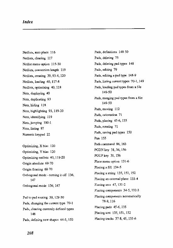
Index
Netlisrs, auto place I 16 Pads, definitions 148-50
Netlists, clearing ll7 Pads, deleting 75
Netlist menu option 115-30 Pads, deleting pad types 148
Netlists, connection length 119 Pads, editing 79
Netlists, creating 39,93-4,120 Pads, editing a pad t'"e 148-9
Nerlists, loading 40, I l7-8 Pads, listing current types 70-1,149
Nerlisrs, optimizing 40, 118 Pads, loading pad types from a file
Nets, displaying 40 149-50
Ners, duplicating 93 Pads, merging pad rypes frqn a file
Nets, hiding I 18 149-50
l',{ers, highlighting 93, I lg-20 Pads' moving ll2
Ners, idenrifying llg Pads' orientation 7l
Ners, jumping 100-l Pads' placing 45-6' 135
Ners, listing 97 Pads' rotating 7l
Numeric keypad, 22 Pads' saving pad types 150
Pan 155
oprimizing, X bias lz0 Path command 86' 163
optimizing, Y bias l2o PGDN key 3 l ' 36' 156
optimizing netlists 40, I lg-20 PGUP key 3l' 156
origin absolure 69-70 Place menu option 131-6
origin floating 69-70 Placing a fill 134-5
orttrogonal mode - tuming it off 136, Placing a string 135' lst' 152
147 Placing an extemal Plane 133-4
orthogonal mode 136, 147 Placing arcs 47, r3l-2
Placing components 34-5, 132-3
pad to pad routing 39, I 29-30 Placing components automatically
Pads, changing the current type 70-1 78-9' I 16
Pads, clearing currently defined types Placing pads 454' 135
148 Placing text 135, l5l,152
pads, defrning new shapes 44-s, ls} Placing tracks 37 -8, 45, 135-6
208
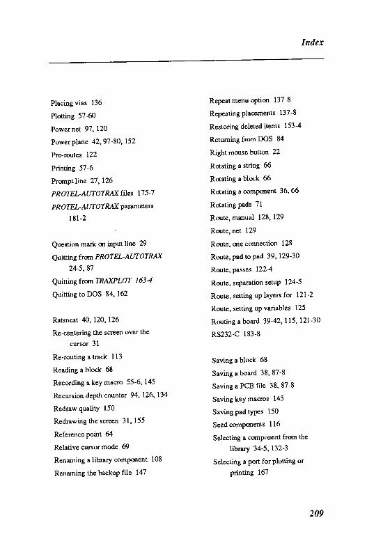
Index
Placing vias 136
Plotting 57 6
Power ner 97,l2O
Power plane 42,97 -80, 152
Pre-route s 122
Printing 57 -6
Prunpt lne 27,126
PROTEL-AWOTRN{ files 17 5-7
P R OTE L- AW OT RN( Parameters
181 -2
Question mark on inPut line 29
Quitting from PROTEbAWOTRN{
24-5, 87
Quitting frqn TRNGI'OT 1634
Quitting to DOS 84,162
Ratsnest N,120, t26
Re-centering the scrcen over the
cursor 31
Re-routing a track 113
Reading a block 68
Recording a key macro 55-6,145
Recursion depth counter 94, 126, 134
Redraw quality 150
Redrawing the scr@n 31, 155
Reference point 64
Relative cursor mode I
Renaming a library comPonent 108
Renaming the backuP file 147
Repeat menu oPtion 137 -8
Repeating placements 137-8
Restoring deleted items 153-4
Retuming from DOS 84
Right mouse button 22
Rotating a string 66
Rotating a block 66
Rotating a comPqlent 36,66
Rotating pads 71
Rotrte, manual 128,129
Route, net 129
Route, one connection 128
Ronte, pad to pad 39, 129-30
Route, passes 122-4
Rorte, separation setuP 124-5
Rotrte, setting uP laYers for l2L-2
Rotrte, setting uP variables 125
Routing a board 39-42, I 15, 121-30
RS232-C 183-8
Saving a block 68
Saving a board 38, 87-8
Saving a PCB file 38, 87-8
Saving key macros 145
Saving pad types 150
Seed components I 16
Selecting a comPonent frsn the
library 34-5, 132-3
Selecting a Port for Plotting or
printing 167
209
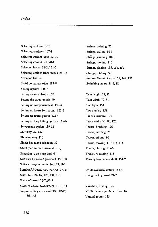
Index
Selecting a plotter 167
Selecting a printer 167 -8
Selecting current layer 32,70
Selecting curent pad 7O-l
Selecting layers 3t-2, l5l-z
Selecting options from menus 24,32
Selection bar 24
Serial communication 183-8
Setting optiors 146-8
Setting string defaults 150
Setting the cursor mode 69
Setting up component text 139-40
Setting up layers for routing l2l-2
Setting up router passes l2Z4
Setting up the plotting options 165-6
Setup menu optiq'r 139-52
Shift key 22,142
Showing nets 120
Single key menu selectiqr 32
SMD (See surface mount device)
Snapping to the snap gnd 44
Software License Agreement 15, 180
Software requirements 14, 178, 180
Starting PROTEL-AWOTRN{ 17, 23
Status lne 24,89, 126, 134, 157
Status of board 26-7 ,97 -8
Status window,TRN{PLOT 16l, 163
Stop recording a macro (CTRL END)
56,145
Strings, deleting 75
Strings, editing 80-l
Strings, jurnping 102
Strings, moving I 13
Strings, placing 135, l5l,152
Strings, rotating 6
Sudace Mount Devices 78, 149, 151
Switching layers 3l-2, 38
Text height 72,81
Text width 72,81
Top layer l5l
Top overlay l5l
Track clearance 125
Track width 71, 80, 125
Tracks, breaking I l0
Tracks, deleting 76
Tracks, editing 80
Tracks, moving 110-l12, ll3
Tracks, placing 135-6
Tracks, re-routing 113
Turning layers on and off l5l-2
Un-delete menu option 153-4
Using the keybo ard 2l-Z
Variables, routing 125
VEGA deluxe graphics driver 16
Vertical routes 123
210

Index
VGA graphics driver 16
Via hole size 72,81-2
Via minimisation 124, 128
Via size 72,81-2,125
Vias, deleting 76
Vias, editing 8l-2
Vias, moving 114
Vias, placing 136
Viewing library components 103-4
Z routes 123
Tnommenu option 155-8
Tmrrl.value 157
Tnomwindow 157-8
Tnomng 25,55,155-8
211


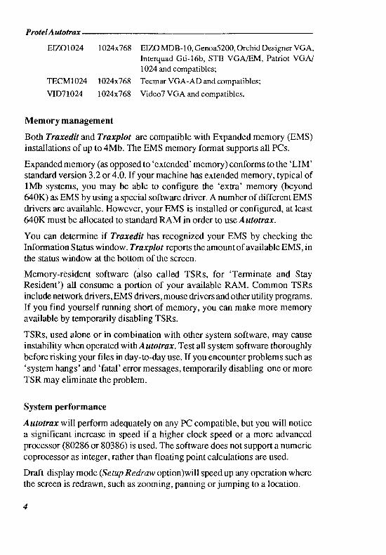
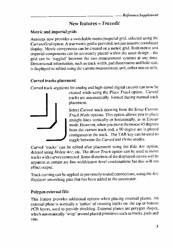


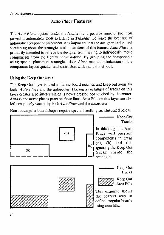


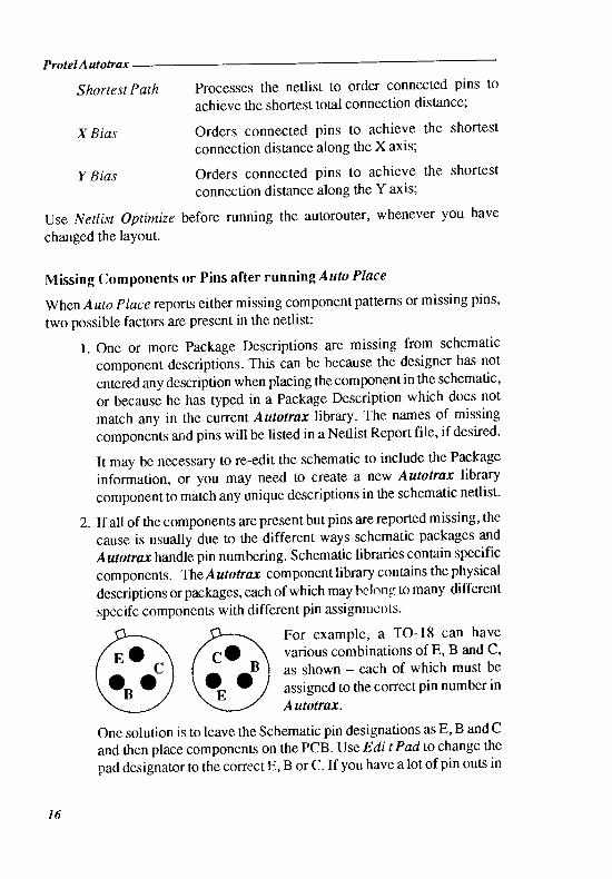

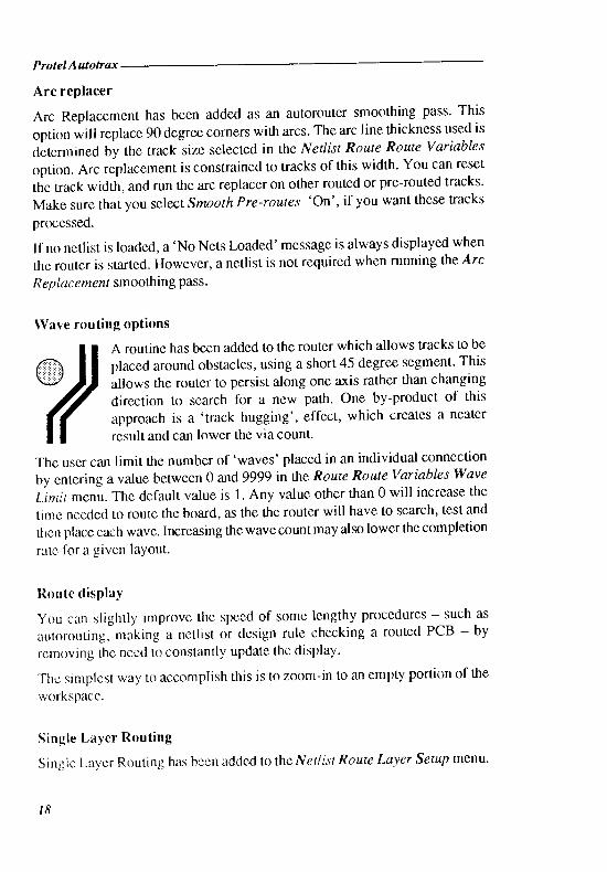

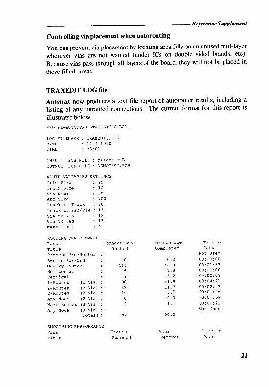


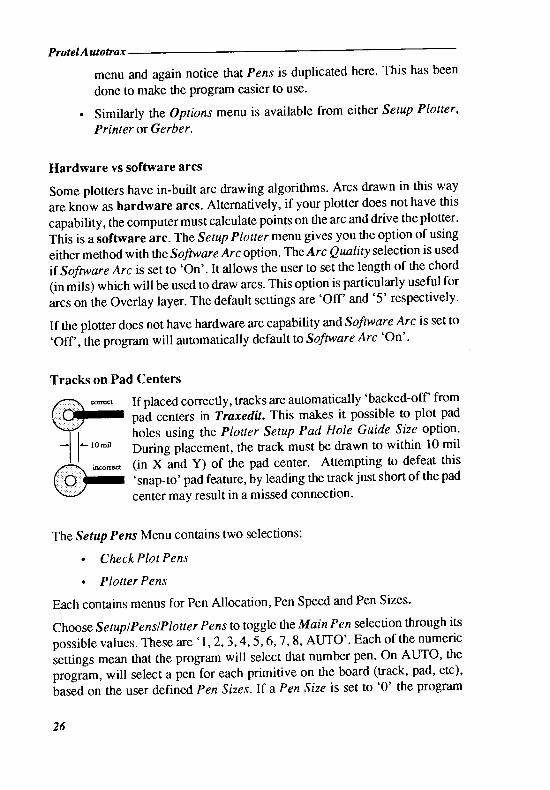

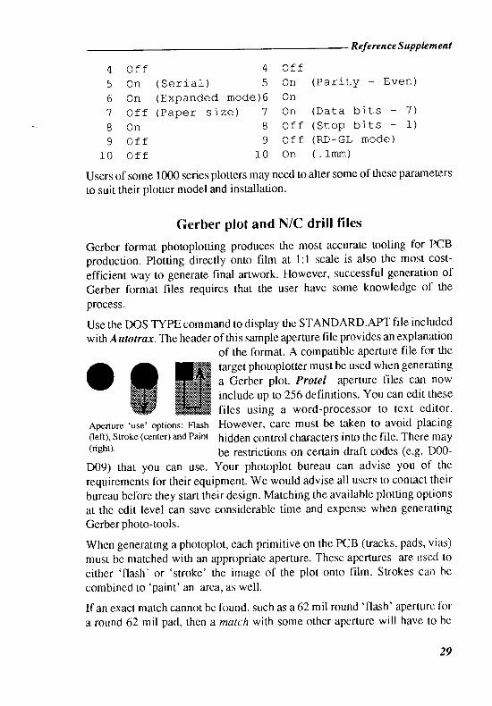
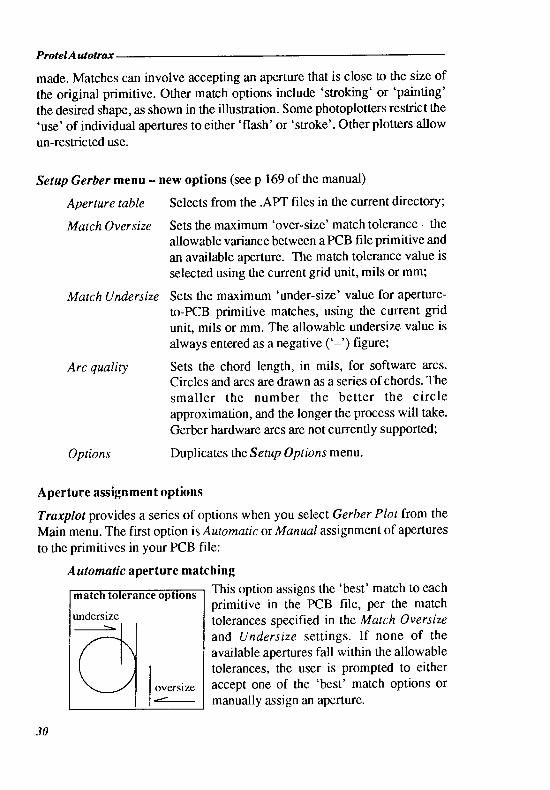


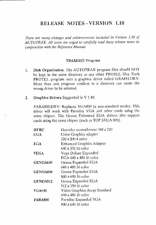
ITELITASII NO'I 'ES . VEITSION [. IO
Tlrcre ere man)t change,s and enhancentents included fu l/ersion LI0 of
AIJT'OTRAX. AIt trsers are urged to corefitlly reod these release noles itt
conjunctiorr witlt tlrc Referetrce Marwal.
TRAXEDIT Program
1. Disk Organizat ion. The AUTO'I 'RAX program f i lcs should NO'f
bc kcpt in the same directory as any other PRO'IEL f i lcs. [ :ach
PROTEL program uses a graphics dr iver cal lcd GRAPH.DRV.
More than one program residcnt in a cl i rectory can cause thc
wrong driver to be selected.
2. Graphics Drivers Supported in V 1.10:
PARA80O.DRV: Replaces VGASffi (a non-standarcl nrodc). T'his
driver wi l l work with Paradise VGA and othcr cards using the
same chipset . The Genoa Enhanccd EGA dr ivcrs a lso support
cards using the same chipset (such as TOP SEGA 800).
I I I IRC I lcrculcs nronocl t ro l l rc 348 x720
CGA Crl lor Graphics i tdaPtcr
EcA i3J',:3::'J;:fiics Adaprcr6q) x 350 16 color
VEGA Vega Deluxe ExpandeclEGA 640 x 480 16 color
GEN0A640 Genoa Expandecl EGA64A x 480 1"6 color
GEN0A800 (ienoa Expandcd EGAB(X) x 6()0 16 color
GEN0A912 Gettoa Expanded EGA912 x 350 16 color
VGA640 Vicleo Graphics Array Standard64{ x 480 16 color
I'ARA800 Paraclise Expanded VGA300 x 6fi) 16 color

3. Setu p/Options Menu addit ions.
a) Flash Cursor On/Off (default is Of|.b) Question Delete An/Off (default is On).
T'RAXEDIT,DFT file changes:
a) .l 'he graphics driver name is now stored in this file. Thisallows changing drivers without losing all settings. Onlycolor sett ings wil l be lost.
tr) The version number is in the file. If the version numberchanges the DF t file will be ignored. There is no need todelete the DFf file unless you wish to restore all settings todcfault.
Stntus l- , ine. Now includcs current T'rack Sizc, current Pad Typcanr l cr r r rcnt Srrap ( i r ic l s ize.
Whi lc us ing I I I ( ; l l l , l ( ; I I ' f , ROU"I 'E or l \ ' IAKE NB' I 'L lS ' l ' yor , l cannow u.se the I 'ollowing commancls: PgUp, PgDn, [{ome, End,Arrorv keys, Zoom menu and Grid menu. The Zaom and Gridmenus may now be used during any command involving a cursormove egi Place/Track, PlacefComponent, etc. The mouse is onlysupported in Zoont/Window.
I l ighl ight Menu addit ion: Reset t l ighl ight turns off highl ight.
Screetr Retlri lw: I l i tt ing the space bar rvil l now tcrminatc screenrcclraws.
EMS: The commands Make Netl ist and Minimize Vias were notworking correctly under EMS in v !.07. These have been corrected.
I f you have EMS instal led then the 32K of DOS memory used tostorc the scrcen image uncler the mcnu is now saved and 32K ofEMS is uscd insteacl.
10. I 'r lrve r antl (lround Planes
Care and forethought is required when planning the use of Powerand (irouncl Planc inner layers. Adequatc clearance must be
4.
5 .
(t.
7.
[J.
9.
nraintainccl aroun(l al l non-conncctccl pin holcs [o cnsurs thatshor ts do not resul t f ronr s l ig l r t nr is-a l ignnrcnt oI laycr .s . ' fhcrecommended minimum for this clearancc is 0.4mm (,016' ' ) forboards less than 305mm (I2") in a side. Largcr boards requirc aclearance o[ at least 0.5mm (.028").
AUTOT'RAX plots a coppcr-frec arca around non-connectcd pinsequal to the pad outside dianreter. Typical pin or lcad diametcrsrequire a 0.7mm (.028) hole. 'fhus,
a standard .A(tT" pad rvil l mcetthis requiremont. T'hese considcrat ion.s musl be appl icd to al lpad/hole combinat ions used in your dcsign.
You can change thcse clcaranccs in a conrplctcd dcsign try rc-edit ing al l pads prior to plott ing thc GND and PWR plane layers.Use thc global edit facil i ty.
11. Keyboard Macros.
When edit ing an exist ing macro or def ining a new one, the Scrol lLock k"y is used to toggle between l i teral and conrmnnd nrode.For example, choosc Setup/Keys/Edit / l ly Name. SclcctPLACE/PAD which corresponds to the < Fl > k.y. You shouldnotice that the sequence o[ cornmands for this macro is: <ESC>< ESC> PP < ENTER > < E,SC> .
The <ESC> and <ENTER> comnrands u 'crc cntercd by h i t t ing<Scrol l Lock> to put the prograrn into l i teral rnode and thcnhi t t ing the <ESC> and <ENTE,R> but tons. This is the only waythat these commands can be used in a macro. I f you entered thecharacter.s r '< I l S C' ' etc. from thc kcyboard rvhi lc in commandmode and saved the result to thc < F'1 > k.y the program wil lintcrprct it as follows:
a) Thcb)
' I 'hc E charactcr rvi l l bc intcrprctccl as thc Erf i t cort tntand.c) The S character wi l l be interpreted as the Str ing cornmand.
and when < Fl> is h i t , you wi l l be in Edi t Str ing mode. Not qui tewhat you were expecting! The AUTOJ'RAX program is delivcredwith a select ion of keyboard macros that approximate the keyboardcommands of PCB version 3.
Users who have previously used the PCB prograrn wil l f ind these
12.
macros very useful. New users have the option to change macros tosuit part icular neccls. I f you wish to change the default pad types orkry macros, simply save your new pad or keyfile toTRAXEDIT.PAD or TRAXEDIT.KEY. The next time you startthe program, this fi le wil l be automatically loaded.
Component Swapping
Thc abi l i ty to swap a component to the other side of thc PCB has
becn expanded to include Through-Hole Devices as well a Surfacetvlounted Devices. To swap component layers, use the Edit/
Component / Layer commands.
Pads
The number of pre-defined Pad types has been reduced to 42. This
al lows the user to clef ine up to 6 customs pads without having to
make any deletions. The following have been removed: SMD20x50, ILound 85, OCT' 85, OCT 225 and SQ 85.
I 'CII3CON (Conversion of PROTEL-PCB fi lcs to AUTOTRAX)
An option has been added to convert PROTEL-PCB v3.lx Dip
Pads to Circular or Rounded Rectangle. Version I .07 ofPCB3CON required use of the BDIT/PAD/GLOBAL command.Note that Dip Pads are converted to Circutar 50 rnils byPCB3CON. If you are using 12 mil tracks we recommend changingPacls to 62 mil Round.
I)ip Pads are now converted to 50 x 120 instead of 40 x I2A.
Keep Out Layer & Board Layer differences
The Keep Out Layer is used to def ine board out l ines and no-go
arcns for thc Auto Placc ancl Autoroutc. Lincs on thi .s laycr arc
never crclssed or touched by the router, Attto Place never places
parts on these lines. Area Fil ls on this layer are left completely
vacant by both Auto Place and Autoroute.
' f 'he Board Layer is lor documentation, dimensions, text and anyothcr iterns that the user doesn't want associated with thc artwork,but may want to plot with a given layer.
13.
14.
L5.
*

16. Deleting nll Free ltrimitives on i l I 'CII
In order to strip all free tracks and Vias, etc from a board withoutremoving the components:
a) Place an Area Fil l (top or bottonr layer) rvhich covers all theprimitives you wish to delcte.
b) Using l l ighl iglr t Net, selcct the Fi l l ( this nray take sometime on large board),
c) Select Delete/I I ighl ight. This wi l l delete al l highl ighteditems except for components.
d) Redraw the screen using the END key.
L7. Deleting Arcs
In PCB Version 3, to delete an arc you had tcl f ind the center. InAUTOTR{K you need to place the cursor on the actual arc.
18. I l ighl ight/Connection
To Fl ighl ight a connect ion, s tar t on a t rack scgment wi th in thatconnection. Highl ight/Connection rvorks outtvarcls unt i l i t rcachcspads, rvhich thc Highl ight rvi l l not pass. I f you start l rom a pad,
Highlight goes nowhere.
19. The Bi l l 0f Materials Fi le.
This f i le is generated by running the BOM.EXE f i le suppl icd onthe PROGRAM DISK A. I )o not nrn I IONI.EXE dut ' ing an ex i t toDOS from either TRAXEDIT or TRAXPLOT. A memory error isl ikely to occur i f this is attempted.
20. Component Library
If you are working through the tutor ial in Ch 3 "Laying out a PCB"you wilt be asked to place a component fronr the l ibrary byentering i ts name "D825". Since the manual was rvr i t ten a number
of DB25 farni ly components havc been addcd, ie: DBzs/lv{,
DR25 lF, DB25RA lNl. Enter thc full name of one of these
connectors and it will be placed successfully.
2L. Nery SIVID components
The components SOT23, SOT143 and SOT 89 have been added tothe standard l ibraries.
AUT'O PLACE Features
7. De l ining a non-rectangular board
Bcfore components can be placed, a board out l ine must be createdin the Keep Out Layer. Using a simple l ine out l ine wi l l not workwhen a non-rectangular board shape is required.
Keep OutTracks
In this diagram, Auto Place will put components in areas (u), (b)and (.).The correct way to define this board shape is:
Keep OutTracks
Keep OutArca Fil ls
/u

2. Auto Place Setup
An explanation of sonlc of thc fcatures of Auto l ] lace/Setup
follows:
a) Large X & Y Placement Grid: Pin 1 (of cotnponcnts with 4
or more pins) wi l l be placed on this gr id.
b) Smal l X & Y Placement Gr id: Pin 1 (of Bypass and Discretc
components) wil l be placed on this grid.
c) Large X & Y Clcarance: When 2 largc components (nf
more than 3 pin.s) arc place,d, lhe clist ance bctrveen t hc
outer edges of ths 2 cornponents inclucl ing ovcrlay laycrs)
wil l be greater or equal to largc clcaranccs.
d) Small X & Y Clearance: Minimum distance between 2 smallcomponents or a small component and a large component.
I typass Cnpncitors, IC's and I 'on'er/ ()round l ' l i tne
lf you need to usc Bypass Capacitors and Polcr or Ground Plancs,
some changcs wi l l bc nccdcd in ordcr to succcssful ly use Auto
Placc.
When Nets are loaded, the Power/Ground Nets are not stored, but
converted to pad attributes. To use Auto Place, loacl Porvcr and
Ground Nets as normal Nets then run Auto Place (n'hich rvi l l look
af ter Bypass Capaci tors) .Clcar Ncts and rc loacl thcm wi th thc
Power and Grouncl Planes assigncd to net nAnlcs.
Auto Place l lypass Capacitor Rules
T'o idcnt i fy Bypass Capacitors, thc progranr f i rst f inds al l
components with 4 or more pins. I t then looks for 2 Nets that go to
70% of thesc components. Thc progranl thcn looks for allcomponents with 2 pins, of rvhich 1 connects to each of these 2Nets. These are identif ied (by Auto Place) as Bypass Capacitors.
Auto Place Discrete Component Rules
Discretc componcnts are lhosc, ot.hcr lhan Bypass Capacitors, that
3.
4.
5.

I tave less than 4 pins. They are assigned to large componcnts by asimple rule. Ignoring the 2 identi f ied power Nets, a Discretecomponent is attached to a large component i t 50% or more of i tspins are connected to the large component. So, a 3 pin Discreterequires 2 connections and aZ pin "discrete" requires L connection.
These Discrete components are then grouped with the associatedlarge component. T'he Bypass Capacitors are added and the wholeunit is placed on the Large X &. Y Grid. With Auto Place sometrial & error is usually required to {ind a combination which issatisfactory. It is recommencled that you save your layout bclorerunning Auto Placc. That wny, i f you don't l ike the result you canreload the {i le and change the setup.
6. l\'Iultiple Libraries with Auto Place
Thc fol lowing procedure allows use of mult iple componentl ibraries with Auto Place.
a) ( io to Librnry/Fi le and sclect thc f i rst required l ibrary.
tr) Run Auto Place / [ ,oad Components. Missing patterns wi l lbe reported at this stage.
c)
d)
Clear the Netlist (Netlist/ Clear),
Return to Library/File and specify new library.
e) Run Auto Place / Load again.
Re-nrnning Auto Place
After components are placed by Auto Place they are "fixed inplace". If no space can be found for a component then it is placedat thc top of the boarcl ancl set to "[ree to nlove". I f you nranual lymove a component then it becomes "fixed in place". The"[ree"
f"f ixed" status of a component can be changed using theEdit/Component/Placement commands. When Auto Place is run,it treats "fixed" components as pre-placed and builds from them.
(iett ing good results from Auto Place
Auto Place locates components logically and conveniently to
7.
B.
faci l i tatc f inal placcrncnt by thc dcsigncr. I ' f SIIOULD NOT IIE
ASSUMED TI{AT TI{E AUTOMATICALI.Y PLACEI)
COMPONENTS WILL ALWAYS BE II{ TI-IE OPTIMUM
POSITION F'OR A GIVEN DESIGN.
9. Netl ist Formats
Nctlists from schcmatic capture packages (othcr than PROT'EL-
SCHEMATIC) may conform generally to the PROTEL Netlist
format. However, package names (DIP40, etc) ancl Pin idcntif icrs
may require editing.
10. Trnnsistors and ot lrer mult i -pin discretcs lrortr Sclrcnrat ic Netl ists
A single Component pattcrn can have many cliffcrent pin out
dcsignations. For cxample, a TO-92 can have various combinations
of E, B and C. One solution is to leave the Schematic pin
designations as E, B and C ancl then place components on thc
PCB. LJse Edit/Pad to change thc pad dcsignator to the correct E,
B or C. If you have a lot of pin outs in ths sanrs orientation, yotl
may want to either make a special component in thc l ibrary with
thc correct dcsignations, or usc Repeat Place alter cclit ing thc first
compongnt.
AUTOROUTER Feittures
1,. Single Layer Routing
Singlc Layer Routing has becn acldcd [o the Netl ist /Route/Layer
Setup menu.
a) Set thc layer you wish to route to Single Lal 'er Routing.
b) Set all clther layers to Layer l'{ot Used.
Smoothing Passes
Four "Srnoothing" Passes have been addcd to the Route menu:
a) Diagonal Remover: removes sl 'rort diagonals which thc
Autorouter has duplicated ovcr a singlc location.
2.

3.
b) Loclp Rcnrovcr: rcmovcs half of an unintcnt ional loopcrcatcd by the Autorouter.
c) Doublc Back Rcmovcr: attcnrpts to rcplacc nccdlcsslyindirect rouLcs with straight track scgments.
c) Dual Stub Remover: attempts to reduce two short stubsconnccting to a pad to a single stub.
Tlvo Via Remol'er
This pass attempts to removc one o[ two connectcd vias whcn theyare within 100 mils of each other.
4, Sett ings for SMD Routing
Try:
Routc Gr id:Route Tracks:Routc Via:Track to Track:Pad to Pad:Pad to Track:
25 mil8 mi l40 mil8 mil clearance8 mil clearanco8 mil clearance
5.
Che ck with your PCB manufacturer bcforc designing to thcsespccs. Sct vcrt ical and horizontal route layers dcpending on howthc boarcl is organizcd. If you havc an array of SMD mcmory chipsarrangecl vcrtically on the top layer, then sct Top Layer to Vertical.
Control l i ng Via l l lacement
Via placement can be controlled by placing Area Fil ls on anunused mid-layer rvherever Vias are not wanted. ( undcr ICs ondouble siclcd boards, etc). Because Vias pass through all layers oft.hc board, thcy wil l ncll bc placed in thcse fi l lccl areas.
PROCESS PRE-ROI-ITES pass in the router has becn improved.You can now complete any part of any net and the router wil lrcconncct around your work.
DRC Clcarances
6.
1.
8.
The clcaranccs in Netl ist/Rout er / Separation also apply to theDesign Rule Check
Log File
As a convenicnce to designcrs of larger boards a Log Filc uti l i tyhas been addcd which produces a text f i le report of Autorouterresults, including a l ist ing of any unrouted connections. The dcfaultfilename for the Log filename in the router is TRAXEDIT.LOG
l ' l i t r f t _ L - l t t . l f u l h l t x 5 l r l l l s T l r : 5 t _ 0 tl - l . l G F t L E I { , { f l [ t t t r t . t f J Gu n r E r l 6 - l t - l 9 B BT l n E t l 0 t 1 ?
l l t f ' U T , t ' C B F I L E r P L Q C t D . f ' C t iU U T P U T . ' , L B F I L E I R I , . T ' C b
r ' t R F 0 R n n i l c E
( l U l a l
t ? U i o )( 7 U l o )( ? U i o f( t U i a )( l U i a )
T o t a l c .
f ' t _ t r F 0 k n R N C E
C o r r t r e c t l o n cl i o r r t e d
I Z 85
l 4B Oq . 1
l 0I
? 8 1
T r o c k rS u a P , ; , e d
6 '7
I2
[ ' e r c e r r t a , l FC o t r r g , l e t e d
4 5 . 4l . B5 . 0
? 8 . 4t r . z
7 . '0 . 4
9 9 , 6
U i a *h e l r ,o ue ,J
t t 1
0
T l r l e i n
[ ' o : 9
0 0 r 0 4 r 0 1
U U t 0 0 t ( r c
l f o t U : . c , t
l l o t U : r : , 1
0 0 r 0 ] t l l
0 0 r 0 0 r u 9
9.
il:i'x::: ::ili::l;'"'
AU'IOT'RAX cornpared to PROTEL-ROUTE
Somc formcr PROTEL-ROUTE users have \&'ondcred whyAUTOTRAX seems slow by comparison. PROTEL-ROUTE is asimplc channcl routcr which has a l ixed grid, f ixed via sizc andIixed track size working in a batch modc. Hence thc data structurcsare highly optimized. AUTOTRAX works with any grid sizc, tracksize, via size, user selected clcarances, and unlike PROTEL-ROUTE, supports EMS and routes 6 layers.

1.
AUTOTR{K routes take longcr to perform, but the final qualityof the route is higher with less clean-up required.
Two things that will improve Router performance:
a) Make sure that you run Netlist /Optimize after using AutoPlace, or after making signiticant charrges to the layout ofthe placed boarcl. This allows the program to adjust itsrouting strategy to the final position of componentsresulting in a more direct path.
b) Minimize the connection distances of discretes, such asresistors. The visible "ratsnest" that is present when youShow/AIl Nets is a good aid in repositioning componcnts.Use the Netlist/ l*ngth command to track changes in thetotal connection length as you manually optimize the loy-out. A lower total connection distance will improve routingspeed.
TRAXT'LO'I I}ROGRAIVI
Menu Dupl icat ions.
a) From the Main Plot Menu select Setup. Notice the Pensselect ion. From the Setup menu select Check Plot. Thc Pensselection appears again. Press < ESC > or right mousebutton. Select Ptotter from the Setup menu and again not icethat Pens is dupl icated here. This has been donedeliberately for your benefit, to make the program easier tousg.
b) Simi lar ly the Opt ions menu isSetup/Plotter, Printer and Gerber.
dupl icated under
Reference Manual Changes.
a) On pg. 165 of the Reference Manual, the Pad l lole Sizeselect ion in the Options menu is now cal led Pad l Iole GuideSize. The size entered here is used only as a guide fordri l l ing. The actual size of the hole to be dri l led is stored inPad Hole Size in the TRAXEDIT program.
2.
3.
b) The Setup Menu on pg. 166 now contains the Pens select ionbetrveen NC Dril l and Menu colors.
c) On pg. 169, in the Gerber Setup menu, the PIot Toleranceoption has been removecl from the program. Two newaddit ions arc Arc Qual i ty and Options.
The Plotter Setup Menu (pg. 161).
Some plotters have in-built arc drawing algorithms. Arcs drarvn inthis way are know as l lardware Arcs. Alternatively, i f your plotterdoes not have this capabil i ty, the computer must calculate pointson the arc and drive the plotter. This is a Sofhvare Arc. The PlotterSetup Menu gives you the option of using either method with theSoftware Arc selection. The Arc Quality selection is uscd ifSoftware Arc is set to ON. It al lows the user to sct thc length of thcchord ( in mi ls) which wi l l be uscd to draw arcs. T'his opt ion isparticularly uscful for arcs on the Overlay laycr. The dcfaultsett ings are OFF and 5 respectively. If the plotter docs not havcFlardware Arc capabil i ty and Softrvarc Arc is sct to OFF, theprogram will recognise this and usc the Soltrvare Arc option.
NC Drill Tool files
I f you cal l your .TOL f i le Dri l l .Tol then i t wi l l be loaded at Startup.In version 1".07 you weren't able to load i t manual ly. This restr ict ionhas been removed.
Tracks on Pad Centers
Tracks arc automatically backcd away fronr thc Pad ccntcrs inorder to plot pad holes (if selected in Plot/Setup). For a track tobc backed away from the center of a pad, the track must end withinl0 nr i l ( in X anr l Y) o[ t f rc pat l ccnlcr . In I ' ( lR 3, lhc t rack had tobe exactly on the pad ccnter. In Autotrax the pad ccnters are nolonger important.
Tlre Gerber Setup Menu (pg. 169)
Thi.s mcnu contains the Arc Qual i ty sclect ion as wc do not supportthe Gcrber format t lardwarc Arc.
4.
5.
6.
7. ' Ihc Setup Pens Menu.
This menu contains two selections:a) Check Plot Pensb) Plotter Pens
ln turn, both of (a) and (b) contain separate rnenu select ions forPen Allocation, Pen Speed and Pen Sizes.
Choose Setup/Pens/Plotter Pens. Toggle the lUain Pen selectionthrough its possible values. These are l, 2, 3, 4, 5, 6, 7, 8, AU'IO.Each of the numeric setting.s mean that the program will select thatnumber pen. On AUTO, thc program, rvill select a pen for cac]rprimitive on the board (track, pad, etc), based on the uscr defincdPen Sizes. If a Pen Size is set to 0 the program assumes that thepen is not being used. Whcn the Main Pen is assigned a valuebetween 1 and 8, TRAXPLOT automatically sets the appropriatePen Size to 30 if it was previously 0. This guards against a 0 pensize setting for a selected pen.
I I i t <ESC>/Right Mouse Button unt i l you are back to the SetupPens Menu. Choose Check Plot Pens. Choose Pen Allocation.When you select a layer the pen value will change. If a layer isassigned a particular pen then the following checks are done. First,a check is made [o see if the layer is ON or OFF. If the laycr is ONthen the Pen Size, for the particular pen, is sct to the default valueof 30. If the layer is OFF the Pen Size remains 0.
Il\{PORTAI.IT
There is quite a difference between PROTEL-PCB version 3PLOT and TRAXPLOT with regard to pen sizes for L:L and 2:Iplots. [n the PCB PLOT program it was necessary to use a .6 penfor 2:7 ancl .3 for 1:L. With TRAXPLOT it is not necessary tochango the pen s ize for d i f fcrcnt SCALES. 'Whi lc i t isrecommended that a.6 pen is used for 2:L and .3 for 1:1" plots, theprogram will calculate the correct nurnber o[ passes for each pensize and scale. If gaps occur between pen passes it is likely that thepen size has been specified larger than it physically is.
It should be noted that al l pen sizes arc measured in MILS. (1 mil= 0.001 inch). Thus a standard .3 mil l imeter size pen would beentered as a 12 mil size pen. (0.3 mm = A.ALZ inch).

The qual i ty of f inal plots is determinsd by three factors, nAnrcly thepetr, ink and fi lm types. In particular, different combinations of inkand fl lm can result in different l ine thicknesses being draln w'iththe same pen. As a result there may be either, small gaps bctrvccnpen passes caused by thinner than expected l ines, or sl ight ly thickerthan expected l ines causing pad hole f i l l - ins. In the l l rst case i twould bc necessary to exper iment wi th pen s ize valucs s l ight lylarger than the actual physical size. In the second, sff ial ler thanactual sizc valucs would be neecled.
8. T'he NC Dri l l Menu.
This select ion is found at the Main Menu level. I t operates in avery similar way to the Gerber Plot menu. Tool numbers and dri l ls izes stored in the Tool Table are matched to pad hole sizes, rvi thina specified tolcrance level. Again these parameters are define d inthe Setup/NC Dri l l menu.
Upon complet ion of matching, two f i les are wr i t ten to d isk, nanrc ly.DRL ar rd .TXT f i les . J 'hc . l )RL f i l c i s in Excc l lon fo rmat . The.TXT is i ts ASCII equivalent.
Confusion over pen sizes in TraxPlot
In TraxPlot the pen size specif ies the width of the l ine that the pcndrarvs. This measuremcnt is in nr i ls ( .000L inch). I f using thc pcn.sf rom PCB 3 the 0.3mm pcn should be set at 13 nr i l and thc 0.6nrnrpcn set at 26 mil. Don't use 30 and 60 rnil for thcse pcn sizcs.
Note also that the Pad l. lole Guide Size, Solder lvlask and PastcMask enlargements are also in mils, not metric.
Software Arc Chord Lcngth is atso measured in mils. At least 6scgmcnts arc now usccl in a circlc, no mattcr how largc thc chorcl i .sset.
10. Culconrp Plotter Driver
The Calcomp driver rvi l l work for both non-intel l igcnt andintel l igent Calcomp plotters using the 960 lormat. At present,software arcs arc used but thc next version rvi l l make usc of t l rcplottcrs' inbui l t arc faci l i ty which wi l l increase the speed of the plot.
9.
The communications menu
0 Parity &Bits/Char
Stop Ilits
Interface
Host Baud& Modc
Muting& Checksum
Isochronous& EOM
f)irect CtrlxoN/xoFF
of lhe plotter must be setup as follows:
Parity = 0 (nonc)Bits/Char = 8
Stop BiLs = L
Interface = 0(Serial)
Host Baud = 24{nMode = 1 (960)
Term Muting = NoCksum enable = No
Isochronous = NoEOM = 03
I)irect Ctrl = YesXON/XOFF = No
1 1 . New option in TraxPlot
The user can now turn off Vias in any Plot or Print. Option is inthe Option menu, under the main Plot lnenu.
The Gerber Plot Menu.
ALJTOTRAX allows ths creation of Gerber format photoplot files.This requires that the operator have some knowledge of thc targetphotoplotter. Specifically, a list of apertures rlefining the size shapeand usage of each must be provided. From DOS, entcr thecommand TYPE PRECISI.AIIT <RET> for an example. This fileincludes an explanation of the format. If you intend to use aphotoplotting bureau, it is necess ary to obtain aperture file formatinformation directly from them.
From the TRAXPLOT Main Menu select Setup/Gerber. Afterproviding the relevant pcb filename and selecting appropriatc Xand Y offsets (often 0.000) the appropriate Aperture Table m ustbe selected. It is important to realize that the apertures available
12.
may not exactly match the pads described by the PCB fi le.
TRAXPLOT wil l automatical ly assign apertures to match padswithin the l l latch Tolerance. In general the match tolerance shouldnot be too l iberal as clearance errors may result . I f unsure then usea Match Tolerance of 5% or less.
G54 should normal ly bc OFF. This is rcqui red by sornc of thc o ldcrplotters to precede aperture change commands.
Circles and arcs are clrawn as a serics of chords. Are Qual i tydetermines the chord length, in mi ls . The smal ler the number ( .g5) the better the circle approximation, and the longer the processwil l take.
Front the Options menu set the type of plot (eg Top Layer) turnot f Bordcr , ' f i t lc
Block, Vias in S<l ldcr Mask (nornra l ly) and sctPad Holc Guidc Siz.c (not appl icablc to photoplot t ing) , Solc ler andltat l M ask Enlargcmcnts to 0.
' l 'hc Soldcr and Pacl lv{ ask
cn la rgcmcn t . s a rc on l y ap l ) l i cab l c t o mask t vpc p lo t s . . I ' hccnlargcmcnt pcrccntagcs ci ln bc rccorn nlcnclcd lry your I tCBmanufacturer.
Return to Main Plot Menu and select File, then Loacl. Supply yourPCB fi lename. The fi le wil l be checked then loaded. Progressinformation is displayccl.
Return again to the Main Plot Menu and select Gerber Plot. Atthis point TRAXPLOT will a.ssign draft codes from the aperturetable to objects fronr the PCB file.The lVlatch Tolerance selcctionallows the user to set the level of matching. This sett ing instructsthe program to match draft codcs with pad sizcs which areapproximately of the same area, within the perccntage error set. Ifno aperture can be found rvithin the Match Tolerance specif ied, theopcrator wil l bc askcd for assistancc. T'RAXPLO'I ' rvi l l providcFlash, Stroke and l?i l l options, or yotr can force some othcr sotutionby sclcct ing manual assignment. Tlr is al lorvs thc choicc of any draftcode ancl any mcthod. A surnmary of matchc.s macle is providcd ina text f i le the name of which is prcscnted to the operator (. lvlAT).
The layer f i le can now be generated. Progress information isdisplayed during this process. To crcate another layer f i le onesimply changes the type of plot in Setup Options, then selects

( lcr l ler Plot from thc Main Plot Mcnu. T'hcrcRcassign Draft Codcs although thc choicc is thcrc.
ntr nccd to
In gcneral if one knows that a particular photoplotter is to be uscdit is a good idea to create a TRAXEDIT component librarycorresponding to the apertures available on that plotter. In this wayIW% match is always assured thus avoidin g any possible toleranceerrors and speeding up the plot by obviating the necessity for timeexpensive fills.