
PM0222 Programming manual - STMicroelectronics · This programming manual targets application...
33
February 2014 DocID025476 Rev 1 1/33 PM0222 Programming manual Brain smart hub family Introduction This programming manual targets application developers and is a supplement to the Brain reference manual, providing complementary information to facilitate device programming. It is highly recommended to read the Brain reference manual before consulting this document. The Brain device belongs to the family of smart hub microcontrollers. It is a low-power device based on Cortex-M0 with 64 Kbyte Flash and 128 Kbyte SRAM and includes several peripherals. For ordering information and mechanical or electrical device characteristics, please refer to the Brain datasheet. www.st.com
Transcript of PM0222 Programming manual - STMicroelectronics · This programming manual targets application...
February 2014 DocID025476 Rev 1 1/33
PM0222Programming manual
Brain smart hub family
IntroductionThis programming manual targets application developers and is a supplement to the Brain reference manual, providing complementary information to facilitate device programming. It is highly recommended to read the Brain reference manual before consulting this document.
The Brain device belongs to the family of smart hub microcontrollers. It is a low-power device based on Cortex-M0 with 64 Kbyte Flash and 128 Kbyte SRAM and includes several peripherals.
For ordering information and mechanical or electrical device characteristics, please refer to the Brain datasheet.
www.st.com
Contents PM0222
2/33 DocID025476 Rev 1
Contents
1 Reference documents . . . . . . . . . . . . . . . . . . . . . . . . . . . . . . . . . . . . . . . . 6
2 Brain status after boot . . . . . . . . . . . . . . . . . . . . . . . . . . . . . . . . . . . . . . . 7
3 Clock configurations . . . . . . . . . . . . . . . . . . . . . . . . . . . . . . . . . . . . . . . . . 83.1 Peripheral clock gating . . . . . . . . . . . . . . . . . . . . . . . . . . . . . . . . . . . . . . . . 8
3.2 CPU clock configuration . . . . . . . . . . . . . . . . . . . . . . . . . . . . . . . . . . . . . . . 83.2.1 Flash wait states . . . . . . . . . . . . . . . . . . . . . . . . . . . . . . . . . . . . . . . . . . . 8
3.2.2 CPU clock table . . . . . . . . . . . . . . . . . . . . . . . . . . . . . . . . . . . . . . . . . . . . 9
3.2.3 Disabling the 80 MHz RC oscillator . . . . . . . . . . . . . . . . . . . . . . . . . . . . 10
4 Interrupt management . . . . . . . . . . . . . . . . . . . . . . . . . . . . . . . . . . . . . . 114.1 Vector table . . . . . . . . . . . . . . . . . . . . . . . . . . . . . . . . . . . . . . . . . . . . . . . 11
4.2 Interrupt activation sequence . . . . . . . . . . . . . . . . . . . . . . . . . . . . . . . . . . 11
5 GPIO / IOs management . . . . . . . . . . . . . . . . . . . . . . . . . . . . . . . . . . . . . 125.1 I/O configuration . . . . . . . . . . . . . . . . . . . . . . . . . . . . . . . . . . . . . . . . . . . . 12
5.1.1 I/O mode . . . . . . . . . . . . . . . . . . . . . . . . . . . . . . . . . . . . . . . . . . . . . . . . 12
5.1.2 Simple I/O configurations . . . . . . . . . . . . . . . . . . . . . . . . . . . . . . . . . . . . 13
5.1.3 Configuration of IO7/8/9/10 to become SPI I/Os . . . . . . . . . . . . . . . . . . 13
5.2 Pull activation . . . . . . . . . . . . . . . . . . . . . . . . . . . . . . . . . . . . . . . . . . . . . . 14
5.3 Shared I/Os at chip level (double bonding) . . . . . . . . . . . . . . . . . . . . . . . 14
6 Flash controller . . . . . . . . . . . . . . . . . . . . . . . . . . . . . . . . . . . . . . . . . . . . 156.1 Default configuration after boot . . . . . . . . . . . . . . . . . . . . . . . . . . . . . . . . 15
6.2 Flash commands (read / write / erase) . . . . . . . . . . . . . . . . . . . . . . . . . . . 156.2.1 General information . . . . . . . . . . . . . . . . . . . . . . . . . . . . . . . . . . . . . . . . 15
6.2.2 Read function examples . . . . . . . . . . . . . . . . . . . . . . . . . . . . . . . . . . . . 15
6.2.3 Erase function examples . . . . . . . . . . . . . . . . . . . . . . . . . . . . . . . . . . . . 16
6.2.4 Write function examples . . . . . . . . . . . . . . . . . . . . . . . . . . . . . . . . . . . . . 17
6.3 Locked / Unlocked feature . . . . . . . . . . . . . . . . . . . . . . . . . . . . . . . . . . . . 18
7 ECC RAM . . . . . . . . . . . . . . . . . . . . . . . . . . . . . . . . . . . . . . . . . . . . . . . . . 197.1 Initialization . . . . . . . . . . . . . . . . . . . . . . . . . . . . . . . . . . . . . . . . . . . . . . . 19
DocID025476 Rev 1 3/33
PM0222 Contents
33
7.2 ECC RAM actions . . . . . . . . . . . . . . . . . . . . . . . . . . . . . . . . . . . . . . . . . . 19
8 Timers . . . . . . . . . . . . . . . . . . . . . . . . . . . . . . . . . . . . . . . . . . . . . . . . . . . . 208.1 Dual timers . . . . . . . . . . . . . . . . . . . . . . . . . . . . . . . . . . . . . . . . . . . . . . . 20
8.1.1 Periodic mode . . . . . . . . . . . . . . . . . . . . . . . . . . . . . . . . . . . . . . . . . . . . 20
8.1.2 One-shot mode . . . . . . . . . . . . . . . . . . . . . . . . . . . . . . . . . . . . . . . . . . . 21
8.2 Watchdog (WDG) . . . . . . . . . . . . . . . . . . . . . . . . . . . . . . . . . . . . . . . . . . . 21
8.3 SysTick . . . . . . . . . . . . . . . . . . . . . . . . . . . . . . . . . . . . . . . . . . . . . . . . . . . 22
9 UART . . . . . . . . . . . . . . . . . . . . . . . . . . . . . . . . . . . . . . . . . . . . . . . . . . . . 239.1 FIFO management . . . . . . . . . . . . . . . . . . . . . . . . . . . . . . . . . . . . . . . . . . 23
9.2 Baud rate calculation example . . . . . . . . . . . . . . . . . . . . . . . . . . . . . . . . . 23
9.3 Basic configuration . . . . . . . . . . . . . . . . . . . . . . . . . . . . . . . . . . . . . . . . . . 24
10 I2C . . . . . . . . . . . . . . . . . . . . . . . . . . . . . . . . . . . . . . . . . . . . . . . . . . . . . . . 2510.1 I2C FIFO management . . . . . . . . . . . . . . . . . . . . . . . . . . . . . . . . . . . . . . . 25
10.2 I2C clock rate calculation example . . . . . . . . . . . . . . . . . . . . . . . . . . . . . . 25
10.3 I2C configuration . . . . . . . . . . . . . . . . . . . . . . . . . . . . . . . . . . . . . . . . . . . . 2610.3.1 I2C master . . . . . . . . . . . . . . . . . . . . . . . . . . . . . . . . . . . . . . . . . . . . . . . 26
10.3.2 I²C slave . . . . . . . . . . . . . . . . . . . . . . . . . . . . . . . . . . . . . . . . . . . . . . . . . 27
10.4 I2C double bonding . . . . . . . . . . . . . . . . . . . . . . . . . . . . . . . . . . . . . . . . . . 2710.4.1 I2C2 . . . . . . . . . . . . . . . . . . . . . . . . . . . . . . . . . . . . . . . . . . . . . . . . . . . . 27
10.4.2 I2C1 . . . . . . . . . . . . . . . . . . . . . . . . . . . . . . . . . . . . . . . . . . . . . . . . . . . . 28
11 SPI . . . . . . . . . . . . . . . . . . . . . . . . . . . . . . . . . . . . . . . . . . . . . . . . . . . . . . . 2911.1 FIFO management . . . . . . . . . . . . . . . . . . . . . . . . . . . . . . . . . . . . . . . . . . 29
11.2 Clock rate calculation example . . . . . . . . . . . . . . . . . . . . . . . . . . . . . . . . . 29
11.3 SPI configuration . . . . . . . . . . . . . . . . . . . . . . . . . . . . . . . . . . . . . . . . . . . 3011.3.1 Master SPI . . . . . . . . . . . . . . . . . . . . . . . . . . . . . . . . . . . . . . . . . . . . . . . 30
11.3.2 Slave SPI . . . . . . . . . . . . . . . . . . . . . . . . . . . . . . . . . . . . . . . . . . . . . . . . 31
12 Revision history . . . . . . . . . . . . . . . . . . . . . . . . . . . . . . . . . . . . . . . . . . . 32

List of tables PM0222
4/33 DocID025476 Rev 1
List of tables
Table 1. Reference documents. . . . . . . . . . . . . . . . . . . . . . . . . . . . . . . . . . . . . . . . . . . . . . . . . . . . . . 6Table 2. Customer code inputs to provide . . . . . . . . . . . . . . . . . . . . . . . . . . . . . . . . . . . . . . . . . . . . . 7Table 3. Default device settings after boot . . . . . . . . . . . . . . . . . . . . . . . . . . . . . . . . . . . . . . . . . . . . . 7Table 4. CPU clock programming. . . . . . . . . . . . . . . . . . . . . . . . . . . . . . . . . . . . . . . . . . . . . . . . . . . . 9Table 5. GPIO modes . . . . . . . . . . . . . . . . . . . . . . . . . . . . . . . . . . . . . . . . . . . . . . . . . . . . . . . . . . . . 12Table 6. IO pull direction. . . . . . . . . . . . . . . . . . . . . . . . . . . . . . . . . . . . . . . . . . . . . . . . . . . . . . . . . . 14Table 7. Document revision history. . . . . . . . . . . . . . . . . . . . . . . . . . . . . . . . . . . . . . . . . . . . . . . . . . 32
DocID025476 Rev 1 5/33
PM0222 List of figures
33
List of figures
Figure 1. GPIO_MODE configuration. . . . . . . . . . . . . . . . . . . . . . . . . . . . . . . . . . . . . . . . . . . . . . . . . 13Figure 2. I2C2 double bonding. . . . . . . . . . . . . . . . . . . . . . . . . . . . . . . . . . . . . . . . . . . . . . . . . . . . . . 28Figure 3. I2C1M double bonding . . . . . . . . . . . . . . . . . . . . . . . . . . . . . . . . . . . . . . . . . . . . . . . . . . . . 28

Reference documents PM0222
6/33 DocID025476 Rev 1
1 Reference documents
Table 1. Reference documentsReference number Name Owner Revision
RM0352 Brain reference manual STMicroelectronics 1.0
DUI0497A_cortex_m0_r0p0_generic_ug(1) “Cortex-M0 Devices Generic User Guide” ARM® r0p0
DDI0419C_arm_architecture_v6m_reference_manual(2) “ARMv6-M Architecture Reference Manual” ARM® C
DDI0194G_ssp_pl022_r1p3_trm(3)
“ARM PrimeCell® Synchronous Serial
Port (PL022) Technical Reference Manual”
ARM® G
1. Refer to http://infocenter.arm.com/help/topic/com.arm.doc.dui0497a/index.html
2. Refer to http://infocenter.arm.com/help/index.jsp?topic=/com.arm.doc.ddi0419c/index.html
3. Refer to http://infocenter.arm.com/help/index.jsp?topic=/com.arm.doc.ddi0194g/index.html
DocID025476 Rev 1 7/33
PM0222 Brain status after boot
33
2 Brain status after boot
To summarize, the Flash memory array in Brain is divided in two blocks: The information block: this section is reserved by STMicroelectronics to store
manufacturing information and proprietary boot code. The main Flash memory containing the customer program and data. This corresponds
to the Flash mentioned throughout this document.
When the reset is released, Cortex-M0 starts to execute the STMicroelectronics proprietary code in the Flash information block.
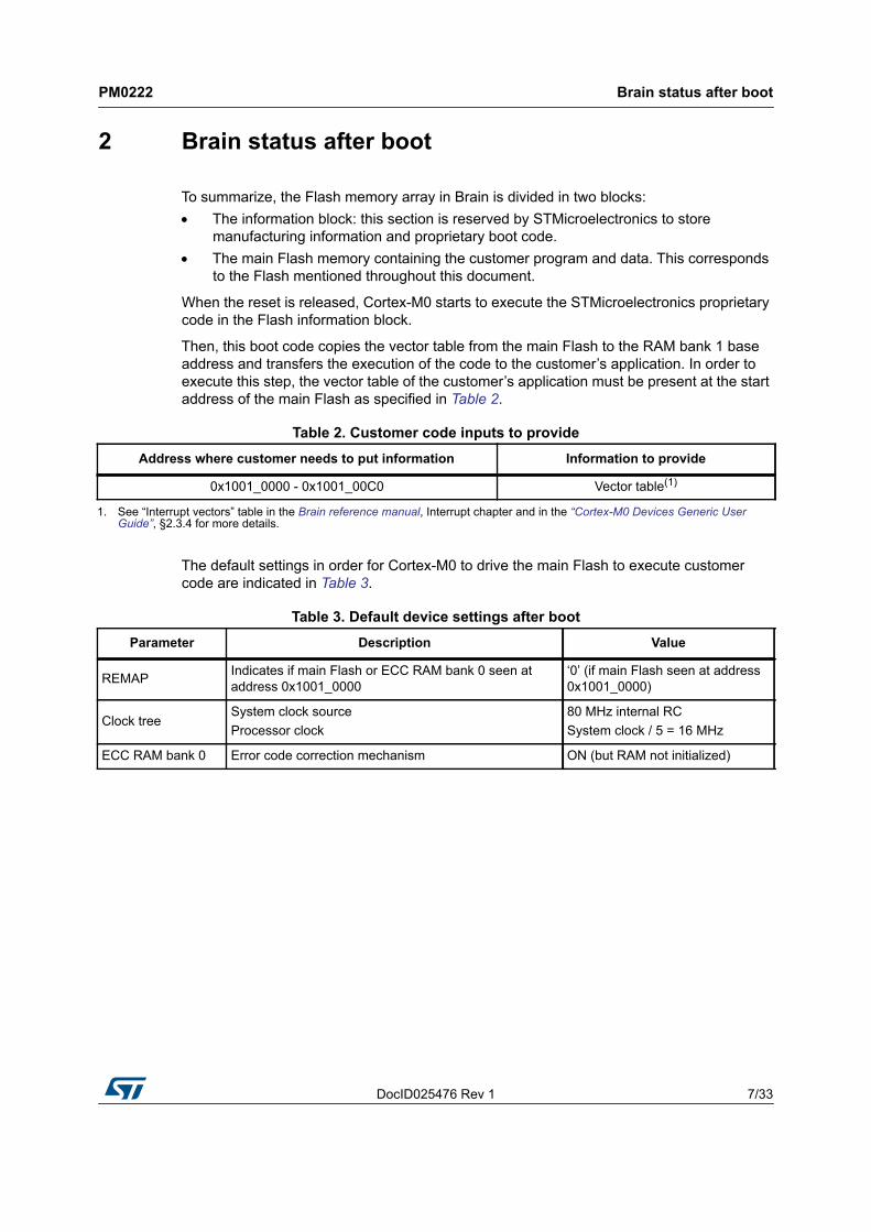
Then, this boot code copies the vector table from the main Flash to the RAM bank 1 base address and transfers the execution of the code to the customer’s application. In order to execute this step, the vector table of the customer’s application must be present at the start address of the main Flash as specified in Table 2.
The default settings in order for Cortex-M0 to drive the main Flash to execute customer code are indicated in Table 3.
Table 2. Customer code inputs to provideAddress where customer needs to put information Information to provide
0x1001_0000 - 0x1001_00C0 Vector table(1)
1. See “Interrupt vectors” table in the Brain reference manual, Interrupt chapter and in the “Cortex-M0 Devices Generic User Guide”, §2.3.4 for more details.
Table 3. Default device settings after bootParameter Description Value
REMAP Indicates if main Flash or ECC RAM bank 0 seen at address 0x1001_0000
‘0’ (if main Flash seen at address 0x1001_0000)
Clock treeSystem clock sourceProcessor clock
80 MHz internal RCSystem clock / 5 = 16 MHz
ECC RAM bank 0 Error code correction mechanism ON (but RAM not initialized)
Clock configurations PM0222
8/33 DocID025476 Rev 1
3 Clock configurations
3.1 Peripheral clock gatingBrain provides a functional clock gating for each peripheral through the CRMU register CCR2. This allows saving power consumption by activating the clock only when a peripheral is in use. It is the role of the software to deactivate the clock of each peripheral as soon as the peripheral is not in use. After a reset, all peripheral clocks are disabled. For more details, see Brain reference manual, CRMU registers chapter, CRMU_CCR2 description.
3.2 CPU clock configurationChanging the CPU clock also impacts the GPIO, SPI and Timer clocks, thus changing data/count rates in these peripherals. For more details about clock generation logic, see Brain reference manual, §5.2.1 - Generic description.
3.2.1 Flash wait statesWhen changing the CPU clock, the software must also change the Flash wait states accordingly before the next Flash read access. Wait states and REGISTERED values to program according to the CPU clock frequency are provided in a table in the Brain reference manual, Embedded Flash memory chapter, CONFIG register description.
Executing from Flash
When executing from Flash, it is mandatory to adjust the number of wait states before changing the CPU clock because Cortex-M0 continuously fetches instructions from Flash. The correct sequence is:
Increase CPU clock frequency:– Set a number of wait states allowed for the new clock frequency by writing to the
FLASH.CONFIG register (see Brain reference manual, Embedded Flash memory chapter, CONFIG register description)
– Set the new higher clock frequency by writing to the CRMU.CCR0 register
Decrease CPU clock frequency:– Set the new lower clock frequency by writing to the CRMU.CCR0 register– Set a number of wait states allowed for the new clock frequency by writing to the
FLASH.CONFIG register (see Brain reference manual, Embedded Flash memory chapter, CONFIG register description)
Executing from RAM
When executing from RAM, no Flash wait state adjustment is necessary when changing the CPU clock until the software needs to read data from Flash in which case, it must:
– either go back to a lower clock frequency compatible with the current wait state configuration (FLASH.CONFIG register)
– or set a wait state configuration compatible with the current clock frequency
DocID025476 Rev 1 9/33
PM0222 Clock configurations
33
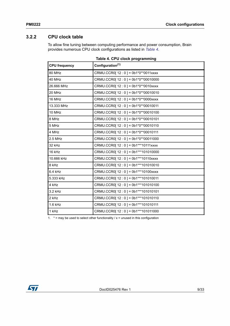
3.2.2 CPU clock tableTo allow fine tuning between computing performance and power consumption, Brain provides numerous CPU clock configurations as listed in Table 4.
Table 4. CPU clock programmingCPU frequency Configuration(1)
1. * = may be used to select other functionality / x = unused in this configuration
80 MHz CRMU.CCR0[ 12 : 0 ] = 0b1*0**0011xxxx
40 MHz CRMU.CCR0[ 12 : 0 ] = 0b1*0**00010000
26.666 MHz CRMU.CCR0[ 12 : 0 ] = 0b1*0**0010xxxx
20 MHz CRMU.CCR0[ 12 : 0 ] = 0b1*0**00010010
16 MHz CRMU.CCR0[ 12 : 0 ] = 0b1*0**0000xxxx
13.333 MHz CRMU.CCR0[ 12 : 0 ] = 0b1*0**00010011
10 MHz CRMU.CCR0[ 12 : 0 ] = 0b1*0**00010100
8 MHz CRMU.CCR0[ 12 : 0 ] = 0b1*0**00010101
5 MHz CRMU.CCR0[ 12 : 0 ] = 0b1*0**00010110
4 MHz CRMU.CCR0[ 12 : 0 ] = 0b1*0**00010111
2.5 MHz CRMU.CCR0[ 12 : 0 ] = 0b1*0**00011000
32 kHz CRMU.CCR0[ 12 : 0 ] = 0b1***10111xxxx
16 kHz CRMU.CCR0[ 12 : 0 ] = 0b1***101010000
10.666 kHz CRMU.CCR0[ 12 : 0 ] = 0b1***10110xxxx
8 kHz CRMU.CCR0[ 12 : 0 ] = 0b1***101010010
6.4 kHz CRMU.CCR0[ 12 : 0 ] = 0b1***10100xxxx
5.333 kHz CRMU.CCR0[ 12 : 0 ] = 0b1***101010011
4 kHz CRMU.CCR0[ 12 : 0 ] = 0b1***101010100
3.2 kHz CRMU.CCR0[ 12 : 0 ] = 0b1***101010101
2 kHz CRMU.CCR0[ 12 : 0 ] = 0b1***101010110
1.6 kHz CRMU.CCR0[ 12 : 0 ] = 0b1***101010111
1 kHz CRMU.CCR0[ 12 : 0 ] = 0b1***101011000

Clock configurations PM0222
10/33 DocID025476 Rev 1
3.2.3 Disabling the 80 MHz RC oscillatorWhen the 80 MHz RC oscillator is not used by the CPU or by any peripheral for a long time, it is recommended to power it down by setting CRMU.CCR0.ANA_PD80M to 1.
When powering down the 80 MHz RC oscillator, the software must change the CPU clock to another source (32 kHz or external) first (CRMU.CCR0.HS_OSC_SEL = 0b01 for example), and then execute a second CRMU register access to power down the oscillator (CRMU.CCR0.ANA_PD80M = 1).
When powering up the 80 MHz RC oscillator, the software can power up the oscillator (CRMU.CCR0.ANA_PD80M = 0) and change the CPU clock to the 80 MHz RC oscillator source at the same time (CRMU.CCR0.HS_OSC_SEL = 0b00).

DocID025476 Rev 1 11/33
PM0222 Interrupt management
33
4 Interrupt management
4.1 Vector tableThe Cortex-M0 vector table is fixed at address 0x0000_0000 (see “Cortex-M0 Devices Generic User Guide”, §2.3.4). At Brain startup, address 0x0000_0000 is located in RAM Bank 1 and the vector table has been copied from the main Flash into RAM bank 1. When an interrupt is triggered, the CPU reads the vector table at 0x0000_0000 which should initially contain a pointer to the user code in Flash.
When needed, the software can write in the vector table located in RAM bank 1 at 0x0000_0000 to dynamically change the IRQ routines.
4.2 Interrupt activation sequenceSafely activating a peripheral interrupt requires the following steps:
– make sure the interrupt is disabled and cleared on the peripheral side (this prevents receiving an interrupt due to a previous event) (see Brain reference manual for each peripheral register map);
– clear pending requests for this interrupt on the Cortex-M0 side using the NVIC ICPR register;
– set the priority using the NVIC IPR0-IPR7 registers;– activate on the Cortex-M0 side using the NVIC ISER register;– activate on the peripheral side
Note that most peripherals require clearing interrupt requests on the peripheral side when handling interrupt service requests to prevent triggering continuous interrupts for the same event.
For more details on the Cortex-M0 exception model, see “ARMv6-M Architecture Reference Manual”, §B1.5.
For more details on Cortex-M0 NVIC behavior and registers, see “ARMv6-M Architecture Reference Manual”, §B3.4.
GPIO / IOs management PM0222
12/33 DocID025476 Rev 1
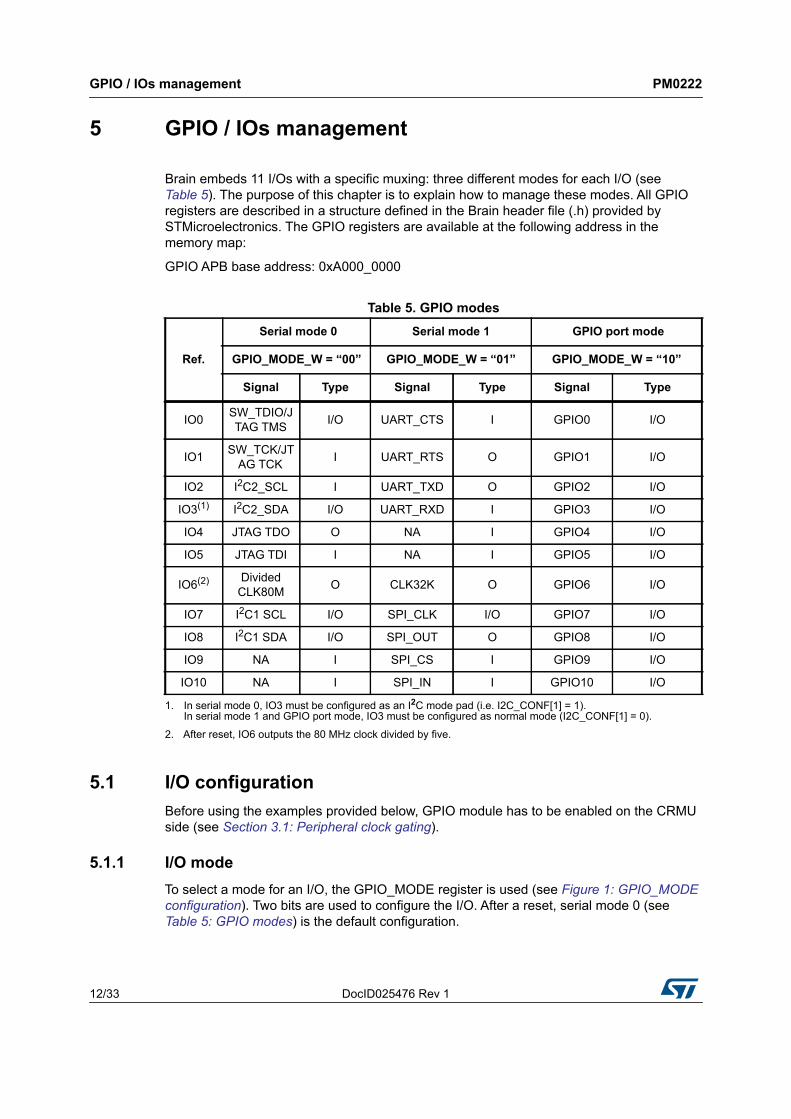
5 GPIO / IOs management
Brain embeds 11 I/Os with a specific muxing: three different modes for each I/O (see Table 5). The purpose of this chapter is to explain how to manage these modes. All GPIO registers are described in a structure defined in the Brain header file (.h) provided by STMicroelectronics. The GPIO registers are available at the following address in the memory map:
GPIO APB base address: 0xA000_0000
5.1 I/O configurationBefore using the examples provided below, GPIO module has to be enabled on the CRMU side (see Section 3.1: Peripheral clock gating).
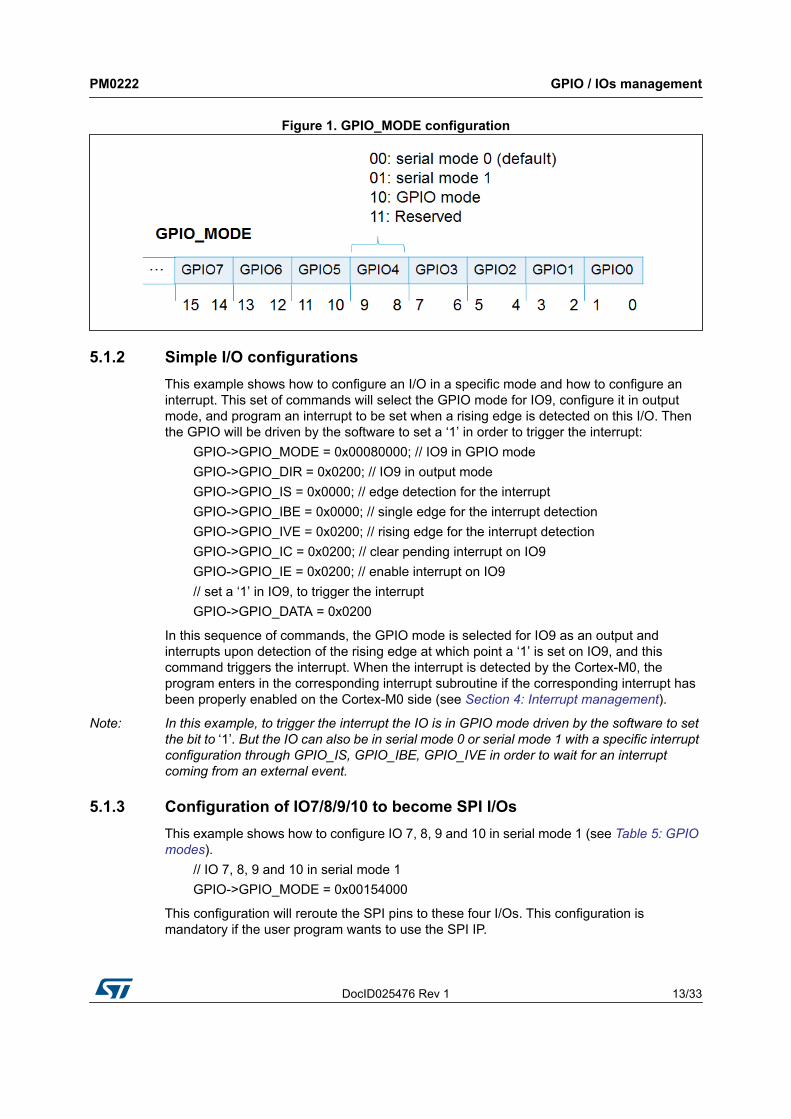
5.1.1 I/O modeTo select a mode for an I/O, the GPIO_MODE register is used (see Figure 1: GPIO_MODE configuration). Two bits are used to configure the I/O. After a reset, serial mode 0 (see Table 5: GPIO modes) is the default configuration.
Table 5. GPIO modes
Ref.
Serial mode 0 Serial mode 1 GPIO port mode
GPIO_MODE_W = “00” GPIO_MODE_W = “01” GPIO_MODE_W = “10”
Signal Type Signal Type Signal Type
IO0 SW_TDIO/JTAG TMS I/O UART_CTS I GPIO0 I/O
IO1 SW_TCK/JTAG TCK I UART_RTS O GPIO1 I/O
IO2 I2C2_SCL I UART_TXD O GPIO2 I/O
IO3(1)
1. In serial mode 0, IO3 must be configured as an I2C mode pad (i.e. I2C_CONF[1] = 1).In serial mode 1 and GPIO port mode, IO3 must be configured as normal mode (I2C_CONF[1] = 0).
I2C2_SDA I/O UART_RXD I GPIO3 I/O
IO4 JTAG TDO O NA I GPIO4 I/O
IO5 JTAG TDI I NA I GPIO5 I/O
IO6(2)
2. After reset, IO6 outputs the 80 MHz clock divided by five.
Divided CLK80M O CLK32K O GPIO6 I/O
IO7 I2C1 SCL I/O SPI_CLK I/O GPIO7 I/O
IO8 I2C1 SDA I/O SPI_OUT O GPIO8 I/O
IO9 NA I SPI_CS I GPIO9 I/O
IO10 NA I SPI_IN I GPIO10 I/O
DocID025476 Rev 1 13/33
PM0222 GPIO / IOs management
33
Figure 1. GPIO_MODE configuration
5.1.2 Simple I/O configurationsThis example shows how to configure an I/O in a specific mode and how to configure an interrupt. This set of commands will select the GPIO mode for IO9, configure it in output mode, and program an interrupt to be set when a rising edge is detected on this I/O. Then the GPIO will be driven by the software to set a ‘1’ in order to trigger the interrupt:
GPIO->GPIO_MODE = 0x00080000; // IO9 in GPIO mode GPIO->GPIO_DIR = 0x0200; // IO9 in output mode GPIO->GPIO_IS = 0x0000; // edge detection for the interrupt GPIO->GPIO_IBE = 0x0000; // single edge for the interrupt detection GPIO->GPIO_IVE = 0x0200; // rising edge for the interrupt detection GPIO->GPIO_IC = 0x0200; // clear pending interrupt on IO9 GPIO->GPIO_IE = 0x0200; // enable interrupt on IO9// set a ‘1’ in IO9, to trigger the interruptGPIO->GPIO_DATA = 0x0200
In this sequence of commands, the GPIO mode is selected for IO9 as an output and interrupts upon detection of the rising edge at which point a ‘1’ is set on IO9, and this command triggers the interrupt. When the interrupt is detected by the Cortex-M0, the program enters in the corresponding interrupt subroutine if the corresponding interrupt has been properly enabled on the Cortex-M0 side (see Section 4: Interrupt management).
Note: In this example, to trigger the interrupt the IO is in GPIO mode driven by the software to set the bit to ‘1’. But the IO can also be in serial mode 0 or serial mode 1 with a specific interrupt configuration through GPIO_IS, GPIO_IBE, GPIO_IVE in order to wait for an interrupt coming from an external event.
5.1.3 Configuration of IO7/8/9/10 to become SPI I/OsThis example shows how to configure IO 7, 8, 9 and 10 in serial mode 1 (see Table 5: GPIO modes).
// IO 7, 8, 9 and 10 in serial mode 1GPIO->GPIO_MODE = 0x00154000
This configuration will reroute the SPI pins to these four I/Os. This configuration is mandatory if the user program wants to use the SPI IP.
GPIO / IOs management PM0222
14/33 DocID025476 Rev 1
5.2 Pull activationEach I/O has a pull-up or a pull-down (fixed). This pull-up/down can be enabled or disabled through the GPIO_PE register (1 bit per I/O). The reset value for this register is 0x3F, meaning the pull (up or down) is enabled for all I/Os after reset. Table 6 indicates the direction of each I/O.
5.3 Shared I/Os at chip level (double bonding)For I²C peripherals there is a double bonding configuration through the I2C_CONF register, see Section 10.4: I2C double bonding.
Table 6. IO pull directionPad reference Pull
IO0 Down
IO1 Down
IO2 Up
IO3 Down
IO4 Down
IO5 Down
IO6 Down
IO7 Up
IO8 Up
IO9 Up
IO10 Down
DocID025476 Rev 1 15/33
PM0222 Flash controller
33
6 Flash controller
Brain embeds 64 Kbyte (16384 x 32-bit) of internal Flash memory. A Flash interface implements instruction access and data access based on the AHB protocol. It implements the logic necessary to carry out the Flash memory operations (Program/Erase) controlled through the Flash registers.
6.1 Default configuration after bootDefault configuration: Flash interface frequency = 80 MHz (internal RC) / 5 = 16 MHz REMAP bit is ‘0’ which means that the main Flash is seen at address 0x1001_0000
6.2 Flash commands (read / write / erase)Precaution for use: for any erase / write action, the system clock must be provided by the internal RC (no external clock configuration).
6.2.1 General informationWriting to Flash only allows clearing bits from ‘1’ to ‘0’. This means any write from ‘0’ to ‘1’implies erasing before performing a write.
Flash memory is composed of 32 pages containing 8 rows of 64 words (32 x 8 x 64 = 16384 words). Each word is 32-bit = 4 bytes long which means 64 KB of Flash.
The address inside the Flash Controller ADDRESS register is built as follows:
ADDRESS[13:0] = XADR[7:0] & YADR[5:0] with XADR[7:3] = page address XADR[2:0] = row address YADR[5:0] = word address (one word = four bytes)
6.2.2 Read function examplesThere are two possible read accesses: Read one single word: simple read as if SRAM memory: read the desired Flash
address and get read data on the bus. MASSREAD command: read the full Flash memory and compare with expected
content
There are two ways of using MASSREAD: Full Flash contains a fixed 32-bit pattern: indicate the expected pattern (value to be
compared with each read value inside Flash) in the Flash Controller DATA register and check the READOK flag in the Flash Controller Interrupt register once the command is completed.
Else: request a MASSREAD command without specifying any expected read value and check the LFSRVAL register once the command is completed. This LFSRVAL register
Flash controller PM0222
16/33 DocID025476 Rev 1
contains a signature of the memory read, built according to the following polynomial: x32 + x31 + x4 + x3 + x1 + 1 (seed value = 0xFFFF_FFFF).
MASSREAD sequence:
– Write in the Flash Controller DATA register the expected value (if MASSREAD is used in combination with the READOK flag).
– Write the MASSREAD command (0x55) in the Flash Controller COMMAND register.
– Wait for the CMDSTART flag in the IRQSTAT register (polling mode or interrupt mode) indicating that the command has been taken into account and is under execution.
– Clear the CMDSTART flag by writing CMDSTART to ‘1’ in the Flash Controller IRQSTAT register.
– Then, wait for the CMDDONE flag in the IRQSTAT register (polling mode or interrupt mode) indicating that the command is completed.
– Check the READOK flag (expected high) in the IRQSTAT register or the LFSRVAL register value to ensure Flash memory content is the expected result.
– Clear the CMDDONE flag by writing CMDDONE to ‘1’ in the Flash Controller IRQSTAT register.
6.2.3 Erase function examplesThe Flash controller allows erasing one page or the full main Flash.
ERASE sequence:
– Write the page address to be erased by writing in the Flash Controller ADDRESS register the following value:ADDRESS[13:9] = XADR[7:3] = page address to eraseADDRESS[8:0] = 9’b0 (row and word addresses at zero).
– Write the ERASE command (0x11) in the Flash Controller COMMAND register.– Wait for the CMDSTART flag in the IRQSTAT register (polling mode or interrupt
mode) indicating command is taken into account and under execution.– Clear the CMDSTART flag by writing CMDSTART to ‘1’ in the Flash Controller
IRQSTAT register.– Wait for the CMDDONE flag in the IRQSTAT register (polling mode or interrupt
mode) indicating that the command is completed.– Clear the CMDDONE flag by writing CMDDONE to ‘1’ in the Flash Controller
IRQSTAT register.– After this command, the erased page will contain only bits set to ‘1’.

DocID025476 Rev 1 17/33
PM0222 Flash controller
33
MASSERASE sequence:
– Write the MASSERASE command (0x22) in the Flash Controller COMMAND register.
– Wait for the CMDSTART flag in the IRQSTAT register (polling mode or interrupt mode) indicating that the command has been taken into account and is under execution.
– Clear the CMDSTART flag by writing CMDSTART to ‘1’ in the Flash Controller IRQSTAT register.
– Wait for the CMDDONE flag in the IRQSTAT register (polling mode or interrupt mode) indicating that the command is completed.
– Clear the CMDDONE flag by writing CMDDONE to ‘1’ in the Flash Controller IRQSTAT register.
– After this command, the full main Flash will contain only bits set to ‘1’.
6.2.4 Write function examplesThe Flash Controller allows writing / programming one word or the full main Flash memory (with a single fixed word).
Note: As a write can only program to ‘0’ on bits already set to ‘1’, it is necessary to erase the page and request that the bits be set to ‘1’ (instead of ‘0’) in order to re-write to ‘0’.
WRITE sequence:
– Indicate the location to write by filling the Flash Controller ADDRESS register with the targeted address (page, row and word number)
– Write the value to program in the Flash Controller DATA register.– Write the WRITE command (0x33) in the Flash Controller COMMAND register.– Wait for the CMDSTART flag in the IRQSTAT register (polling mode or interrupt
mode) indicating that the command has been taken into account and is under execution.
– Clear the CMDSTART flag by writing CMDSTART to ‘1’ in the Flash Controller IRQSTAT register.
– Wait for the CMDDONE flag in the IRQSTAT register (polling mode or interrupt mode) indicating that the command is completed.
– Clear the CMDDONE flag by writing CMDDONE to ‘1’ in the Flash Controller IRQSTAT register.

Flash controller PM0222
18/33 DocID025476 Rev 1
MASSWRITE sequence:
– Write the unique value to program in all the main Flash memory in the Flash Controller DATA register.
– Write the MASSWRITE command (0x44) in the Flash Controller COMMAND register.
– Wait for the CMDSTART flag in the IRQSTAT register (polling mode or interrupt mode) indicating that the command has been taken into account and is under execution.
– Clear the CMDSTART flag by writing CMDSTART to ‘1’ in the Flash Controller IRQSTAT register.
– Wait for the CMDDONE flag in the IRQSTAT register (polling mode or interrupt mode), indicating that the command is completed.
– Clear the CMDDONE flag by writing CMDDONE to ‘1’ in the Flash Controller IRQSTAT register.
6.3 Locked / Unlocked featureFlash memory is protected from a read when the device is in debug mode. This means as soon as Cortex-M0 is halted, any access to Flash memory will return a fixed 0x0 value and generate an AHB error if the debugger tries to read it.
Note that RAM bank0 and RAM bank1 memories are also concerned by this lock protection.
To unlock the Flash and RAM memories and render them readable through JTAG, it is necessary to fill UNLOCKM and UNLOCKL with the 64-bit unlock code. This code corresponds to the two last words inside the main Flash so the condition to unlock them is: UNLOCKM[31:0] = value at address 0x1001_FFF8 (if REMAP = ‘0’ else 0x1002_FFF8) UNLOCKL[31:0] = value at address 0x1001_FFFC (if REMAP = ‘0’ else 0x1002_FFFC)
The 64-bit code in Flash (the two last words inside the memory) is latched automatically before the Cortex-M0 reset is released.
The default value in the UNLOCKM and UNLOCKL registers is 0xFFFF_FFFF corresponding to unwritten or erased Flash. As soon as the customer modifies the two last words inside Flash memory, he will need to program the UNLOCKM and UNLOCKL registers to be able to access Flash and RAM in debug mode.
This UNLOCKM / UNLOCKL register programming can be done through JTAG at the beginning of the debugging session.
Caution: The UNLOCKM and UNLOCKL registers of the Flash Controller can be written only once after reset. Any further write will not be taken into account.
Note: This lock protection has no impact for Flash / RAM read by Cortex-M0 in a non-test mode. It concerns only debug mode.

DocID025476 Rev 1 19/33
PM0222 ECC RAM
33
7 ECC RAM
7.1 Initialization To avoid any unexpected ECC error detection, it is mandatory to initialize ECC RAM bank 0 before any read from it. To summarize, the rule is that any data in RAM bank 0 must be written to before performing the first read.
If full main Flash is copied inside RAM bank 0 and the code execution in RAM is switched, then no additional sequence is required.
If the application is not suited to the rule, an initialization sequence must be performed. An easy method would be to fill the full RAM bank 0 with a fixed pattern (all bits to ‘0’ for instance) before using it.
While executed in main Flash, the customer application must not use RAM bank 0 as a data area that could be read from before a write is performed (heap / variables area, etc.)
7.2 ECC RAM actionsIf a single error is detected on a read access, the ECC mechanism:
– Generates an interrupt (position 10 in the NVIC).– Puts on the bus a corrected version of the data to be read. However, data is not
corrected inside the RAM and needs to be re-written by the user.– Provides status information available in the CRMU_ECCR0 register (it indicates
which address generated the error and which bit position in the data is corrupt). For more details, see Brain reference manual, CRMU registers chapter, CRMU_ECCR0 description.
Note: This status register (CRMU_ECCR0) is cleared when read so take care to save the full information of the read.
If a double error is detected on a read, the ECC mechanism:– Generates a reset– Puts 0xDEAD_DEAD on the data bus– After reset, CRMU_REASON_RESET indicates that ECC is responsible for the
reset and the CRMU_ECCR0 register indicates which RAM address generated the error and which bits in the words were corrupted. For more details, see Brain reference manual, CRMU registers chapter, CRMU_REASON_RESET and CRMU_ECCR0 descriptions.
Note: The CRMU_ECCR0 register is not reset by the ECC reset, so the status is still available after reset.
Note: The CRMU_ECCR0 register is cleared when read, so take care to save the full information of the read.

Timers PM0222
20/33 DocID025476 Rev 1
8 Timers
8.1 Dual timers All dual-timer registers are described in a structure defined in the Brain header file (.h) provided by STMicroelectronics.
Brain has eight SP804 dual-timers available at the following addresses in the memory map: DUALTIMER0 APB base address: 0xA640_0000 DUALTIMER1 APB base address: 0xA740_0000 DUALTIMER2 APB base address: 0xA840_0000 DUALTIMER3 APB base address: 0xA940_0000 DUALTIMER4 APB base address: 0xA680_0000 DUALTIMER5 APB base address: 0xA780_0000 DUALTIMER6 APB base address: 0xA880_0000 DUALTIMER7 APB base address: 0xA980_0000
Dual-timers 0 to 3 are clocked by a clock synchronous to the processor clock. Dual-timers 4 to 7 are clocked by the RC 32 kHz resynchronized on the system clock.
Note: When the processor clock is lower than or equal to 32 kHz, dual-timers 4 to 7 are not functional.
Each dual-timer has two timers referred to as “Timer1” and “Timer2” (or A and B in the interrupt vector table in the Brain reference manual). This section provides a short overview on the use of a dual-timer. In the following examples Timer1 of dual-timer0 is used to run in a periodic/one-shot mode and send an interrupt when the timer reaches zero.
Before using these examples dual-timer0 clock has to be enabled in the CRMU (see Section 3.1: Peripheral clock gating) and the processor clock has to be properly configured (see Section 3.2: CPU clock configuration) according to the user’s program specifications. The specific interrupt for dual-timer0 has to be enabled on the Cortex-M0 side (see Section 4: Interrupt management).
8.1.1 Periodic mode// disable the timer1 of dual-timer0, and all previous configurations in case of a// previous use.DUALTIMER0->Timer1Control = 0x00;DUALTIMER0->Timer1Load = 0x800000; // load a new timer value.
Then to launch the timer, the Timer1Control register has to be configured. In this example the timer1 configuration is: 32-bit mode No division on timer1 incoming clock Interrupt is enabled for timer1 Periodic mode and timer1 are enabled.
DocID025476 Rev 1 21/33
PM0222 Timers
33
See Brain reference manual, Dual timer module chapter, Register descriptions sub-chapter for more details.
// timer configuration, after this command the timer is launched.DUALTIMER0->Timer1Control = 0xE3
Every 8388608 (0x800000) tick periods the timer will reach zero and generate an interrupt. The Timer1Value register contains the current value of the timer. It can be read at any moment when the timer is running.
current = DUALTIMER0->Timer1Value; // save current timer value.
8.1.2 One-shot mode// disable the timer1 of dual-timer0, and all previous configurations in case of a// previous use.DUALTIMER0->Timer1Control = 0x00;DUALTIMER0->Timer1Load = 0x800000; // load a new timer value
Then to launch the timer, the Timer1Control register has to be configured. In this example the timer1 configuration is: 32-bit mode No division on timer1 incoming clock Interrupt is enabled for timer1 One-shot mode and timer1 are enabled.
See Brain reference manual, Dual timer module chapter, Register descriptions sub-chapter for more details.
// timer configuration, after this command the timer is launched.DUALTIMER0->Timer1Control = 0xE2
After 8388608 (0x800000) tick periods the timer will reach zero and generate an interrupt. The Timer1Value register contains the current value of the timer. It can be read at any moment when the timer is running.
current = DUALTIMER0->Timer1Value;// save current timer value
At this stage, writing a new value in the Timer1Load register will restart the timer1 with this new value and stop again when it reaches zero.
At any moment in both configurations the timer1 can be stopped by writing 0x00 in the Timer1Control register.
8.2 Watchdog (WDG)All watchdog registers are described in a structure defined in the Brain header file (.h) provided by STMicroelectronics.
The watchdog APB base address: 0xAA00_0000
The watchdog timer is clocked by the 32 kHz clock.
The watchdog peripheral clock should be enabled on the CRMU side (see Section 3.1: Peripheral clock gating) and the corresponding interrupt should be enabled on the Cortex-
Timers PM0222
22/33 DocID025476 Rev 1
M0 side (see Section 4: Interrupt management). To initiate the IP there are three important registers: WDT_LR: which contains the value to load in the timer (when this register is written, the
counter is immediately restarted from the new value) WDT_CR: which configures the action to process in case the WDG timer reaches zero
(generation of an interrupt or a reset) WDT_ICR: writing to this register will clear the watchdog interrupt and reload the
counter from the WDT_LR register.
8.3 SysTickThe Cortex-M0 in Brain provides a SysTick timer. See Brain reference manual, System timer chapter for more details.
The SysTick timer is clocked by the CPU clock.
All SysTick registers are available through a structure defined in core_cm0.h (Cortex-M0 header provided by ARM). This example will use this set of registers to configure the Systick with the biggest value and launch it:
Disable the SysTick and the previous configuration (in case of previous use): SysTick->CTRL= 0x0; // stop the SysTick timer
In this example the SysTick is initialized with the maximum value: SysTick->LOAD= 0x0FFFFFF; // load value in the SysTick timer
After 16777215 tick periods the counter will reach the targeted value in the LOAD register. Then enable the counter on the CPU clock:
0x1 | 0x1 << 1 | 0x1 << 2; // enable the counter, enable the interrupt and select the processor clock
The VAL register contains the current value of the SysTick counter. A read from this register returns the number of tick periods since the timer has been launched (note that when the counter reaches the targeted value, it restarts):
current = SysTick->VAL; // save the SysTick timer value
DocID025476 Rev 1 23/33
PM0222 UART
33
9 UART
All UART registers are described in a structure defined in the Brain header file (.h) provided by STMicroelectronics.
Brain has one UART available at the following address in the memory map:
UART APB base address: 0xA200_0000
9.1 FIFO managementThe transmit and receive paths are buffered with internal FIFO memory enabling up to 32 bytes to be stored independently in both transmit and receive modes.
9.2 Baud rate calculation exampleTo define the UART baud rate generation there are two registers to configure, UARTIBRD and UARTFBRD. Those two registers contain respectively the decimal and the fractional part of the BAUDDIV data. We can calculate this data using the following formula:
BAUDDIV = ( FUARTCLK / (16 x Baud rate) )
With: FUARTCLK is the UART reference clock frequency. It corresponds to the processor
clock divided by a programmable value from 2 to 127 (see Brain reference manual, Clock and reset management unit chapter for more details).
Baud rate is the Baud rate required by the user’s program
The UARTFBRD field value is calculated as follows:integer(fractional part of BAUDDIV * 64 + 0.5)
Example: calculating the divisor value
If the requested baud rate is 230400 and FUARTCLK = 4 MHz then: BAUDDIV = ( 4 x 10⁶ ) / ( 16 x 230400 ) = 1.085
This means that the decimal part BDRI = 1 and the fractional part BDRF = 0.085.UART->UARTIBRD = 0x1; // configure the integer part of BAUDDIVUART->UARTFBRD = 0x5; // configure the fractional part of BAUDDIV
See Brain reference manual, UART chapter, UARTFBRD register description for more details.
UART PM0222
24/33 DocID025476 Rev 1
9.3 Basic configurationBefore using the previous examples, the UART module has to be enabled in the CRMU (see Section 3.1: Peripheral clock gating) and the correct mode has to be configured for the corresponding IO (see Section 5.1.1: I/O mode).
There are four important registers: UARTIBRD and UARTFBRD to configure the baud rate (see Section 9.2: Baud rate
calculation example or Brain reference manual, UART chapter, UARTFBRD register description for more details)
UARTLCR_H to define the data size UARTCR to enable the IP and the transmitter and receiver mode (both modes can be
enabled at the same time). A write to the transmit FIFO through the UARTDR register triggers a transaction. A read from the receive FIFO through the UARTDR will return the first data received.
This sequence below shows how to configure the UART to put it in receiver and transmitter mode:
UART->UARTCR &= 0xFE; // disable the UARTUART-> UARTLCR_H &= 0x7; // disable and flush the FIFOsUART->UARTCR |= 0x300; // UART in receiver and transmitter modeUART-> UARTLCR_H |= 0x8; // enable the FIFOsUART-> UARTLCR_H |= 0x60; // data transfer of 8 bitsUART->UARTIBRD = 0x1; // UART baud rate configuration, integer partUART->UARTFBRD = 0x5; // UART baud rate configuration, fractional partUART->UARTCR |= 0x1; // enable the UART
After this configuration the UART is able to work as a receiver and a transmitter, generating a specific baud rate (see Section 9.2: Baud rate calculation example). To manage data transfer, the UARTFR register contains a status bit concerning FIFO. A simple configuration for a data transmission is:
- Wait until the UART busy flag (BUSY) goes low
- Write in the transmit FIFO to trigger the transaction and send data.
DocID025476 Rev 1 25/33
PM0222 I2C
33
10 I2C
All I²C registers are described in a structure defined in the Brain header file (.h) provided by STMicroelectronics. Each I²C can operate in master or slave mode, up to 400 kHz (fast mode). Standard mode is also supported up to 100 kHz.
Brain has two I²C available at the following addresses in the memory map: I2C2 APB base address: 0xA400_0000 I2C1 APB base address: 0xA500_0000
10.1 I2C FIFO managementThe transmit and receive paths are buffered with internal FIFO memory enabling up to 16 bytes to be stored independently in both transmit and receive modes.
FIFOs status can be checked using the I²C interrupts. There is a programmable threshold value for each FIFO. When the number of entries is greater for the receive FIFO or less for the transmit FIFO, an interrupt is set.
10.2 I2C clock rate calculation exampleTo define the I²C clock rate generation there is one register to configure: I2C_BRCR.
The clock rate can be calculated using this formula:Clock rate = FI2CCLK / ( (BRCNT2 x 2) + Foncycle ) ) (standard mode)Clock rate = FI2CCLK / ( (BRCNT2 x 3) + Foncycle ) ) (fast mode)
where: FI2CCLK is the I²C reference clock frequency, clocked on the system clock divided by
three BRCNT2 is a field of the I2C_BRCR register Foncycle depends on a programmable field of the I2C_CR register:
I2C_CR: FON = “00” => Filter the clock spike wide = 0 => Foncycle = 1I2C_CR: FON = “01” => Filter the clock spike wide = 1 => Foncycle = 3I2C_CR: FON = “10” => Filter the clock spike wide = 2 => Foncycle = 4I2C_CR: FON = “11” => Filter the clock spike wide = 4 => Foncycle = 6
Example: programming a clock rate
If the system clock is the RC80Mhz: FI2CCLK = 26.66 MHz and we need a 300 kHz I²C clock rate without font cycle in fast mode.
According to the previous equation in fast mode: 0.300 = 26.66 / ((BRCNT2 x 3) + 1)BRCNT2 = (26.66 – 0.3) / 0.9 = 29.2 = 0x1D
This equation provides a theoretical value. The baud rate actually generated on the master clock line may differ due to the charge on the I2C bus or due to the bounding choice (open-drain or push-pull I/Os).
I2C PM0222
26/33 DocID025476 Rev 1
10.3 I2C configurationFollowing a reset, the I²C logic is disabled and must be configured when in this state.
The control register (I2C_CR) and baud rate register (I2C_BRCR) need to be programmed to configure the following parameters of the peripheral: Master or slave 7- or 10-bit addressing mode Speed mode Clock rate
Note: If in slave mode, the I2C_SCR register has to be programmed with the selected slave address.
Then if in master mode, the I2C_MCR register is used to define the transaction: Read or write Slave addresses (7- or 10-bit) to communicate with Addressing a 7- or 10-bit slave address Stop condition, to generate a stop or restart condition at the end of the transaction (for
consecutive transactions) Transaction length
Note: For a master write, the data to transmit have to be written to the transmit FIFO in the I2C_TFR register. For a master read, when the master transaction is done, data are available in the receive FIFO in I2C_RFR.
Before using these examples the I²C module has to be enabled on the CRMU (see Section 3.1: Peripheral clock gating) and the correct mode has to be configured for the corresponding IO (see Section 5.1.1: I/O mode).
10.3.1 I2C masterThis section will show an example as follows: Configure the I2C2 IP in master mode with 300 kHz in fast mode Launch a master write operation of one 8-bit data (0x18), to a slave addressed at 0x1D,
in 7-bit addressing mode // define the I²C clock rate// (see calculation in Section 10.2: I2C clock rate calculation example).I2C2->I2C_BRCR = 0x1D// enable the peripheral; select the master mode and the fast mode for the baud// rate generation I2C2->I2C_CR = 0x01 + (0x1<<1) + (0x1<<4)
Once the I²C peripheral is correctly initiated, the I2C_MCR register has to be configured to begin a transaction.
// write operation, slave address, 7-bit addressing mode, stop condition generated,// transaction lengthI2C2->I2C_MCR = (0x0) + (0x1D<<1) + (0x1<<12) + (0x1<<14) + (0x1<<15) I2C2->I2C_TFR = 0x18; // load the data to send in transmit FIFO

DocID025476 Rev 1 27/33
PM0222 I2C
33
This sequence will trigger a master write operation of one data present in the transmit FIFO to a slave I²C device addressed by 0x1D. The I2C_SR register contains information concerning the status of the transaction: Operation type (master-read, master-write, write-to-slave and read-from-slave). Status (successful, abort) Cause of the abort Length of the transaction
This information will help to determine the next operation. For example, in case of an abort status, the program may retry starting the transaction.
10.3.2 I²C slaveThis section will show an example of configuring the I2C2 IP in slave mode with a 7-bit address 0x1E.
// enable the peripheral; select the master mode, 7-bit addressing mode and the fast// mode for the baud rate generationI2C2->I2C_CR = 0x01 + (0x0<<1) + (0x0<<3) + (0x1<<4) I2C2->I2C_SCR = 0x1E; // define the slave address
After this configuration the I2C2 is ready to work as a slave. Check the I2C_SR register to get the status of the transaction (see Section 10.3.1: I2C master).
10.4 I2C double bonding
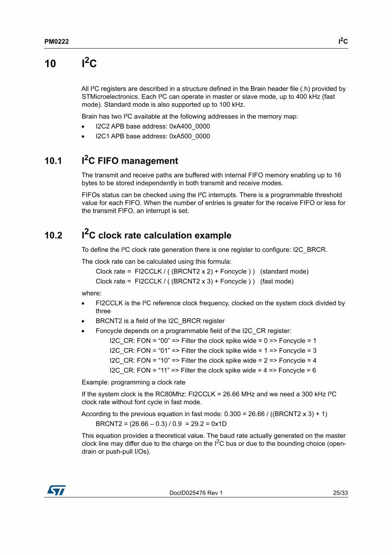
10.4.1 I2C2The first bit of the I2C_CONF register (see Brain reference manual, GPIO chapter) is used to reroute the I2C2 pins. After reset, this bit is configured as one, which means the I2C2 pins are rerouted through MCL and MDA, specific open-drain I/Os. If this bit is set to zero, the I2C2 pins are rerouted to digital standard push-pull I/Os. In both configurations, IO7 and IO8 have to be in serial mode 0 (see Section 5.1.1: I/O mode) to access the I2C2 pins, according to the configuration of the I2C_CONF register.
I2C PM0222
28/33 DocID025476 Rev 1
Figure 2. I2C2 double bonding
Note: In serial mode 0, it is recommended to select the open-drain I/O configuration (I2C_CONFIG[0]) = ‘1’ and push-pull I/Os configuration (I2C_CONFIG[0] = ‘0’) for the other mode.
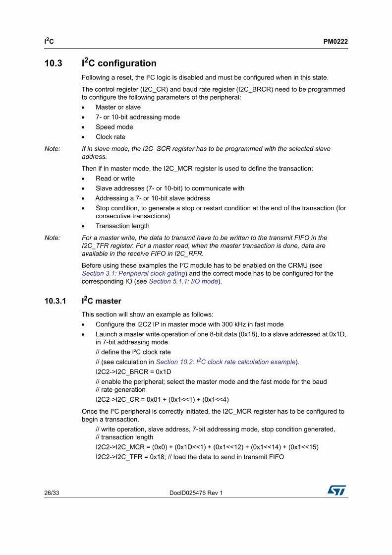
10.4.2 I2C1The second bit of the I2C_CONF register (see Brain reference manual, GPIO chapter) is used to select between an open-drain and a push-pull I/O for the I2C1 SDA line. I2C_CONF[1] = ‘1’ selects the open-drain I/O while I2C_CONF[1] = ‘0’ selects the push-pull I/O. Once this configuration is selected, the serial mode 0 (see Section 5.1.1: I/O mode) has to be selected for IO2 and IO3 to access the I2C1.
Figure 3. I2C1M double bonding
Note: In serial mode 0, it is recommended to select the open-drain I/O configuration (I2C_CONFIG[1]) = ‘1’ and the push-pull I/Os configuration (I2C_CONFIG[1] = ‘0’) for the other mode.
DocID025476 Rev 1 29/33
PM0222 SPI
33
11 SPI
All SPI registers are described in a structure defined in the Brain header file (.h) provided by STMicroelectronics.
Brain has one SPI available at the following address in the memory map:
SPI APB base address: 0xA300_0000
11.1 FIFO managementThe transmit and receive paths are buffered with internal FIFO memory enabling up to 16 bytes to be stored independently in both transmit and receive modes..
FIFO status can be checked using the SSPSR register. It contains status about full/empty FIFO conditions. There are also two interrupts which can be set when the transmit FIFO is half empty and when the receive FIFO is half full. This set of information is useful to manage large data transfers.
11.2 Clock rate calculation exampleThere are two fields that define the SPI baud rate: the SCR field in the SSPCR0 register and the CPSDVR field in the SSPCPSR register.
We can calculate the clock rate using this formula:Clock rate = FSSPCLK / (CPSDVR x ( SCR + 1 ) )
where: FSSPCLK is the SPI reference clock frequency, clocked on the processor clock (see
Brain reference manual, Clock and reset management unit chapter) CPSDVR is an even value from 2-254 programmed in the SSPCPSR register SCR is a value from 0-255 programmed in the SSPCR0 register
Example: programming a clock rateIf the FSSPCLK = 16 MHz and the CPSDVR = 2 then: the clock rate has a frequency range from 8 MHz (SCR = 0) to 31.25 kHz (SCR = 255).
Note: In master mode the processor clock frequency must be at least two times bigger than the SPI clock rate.
Note: In slave mode the clock rate must be twelve times smaller than the processor clock frequency to guarantee the data transfer.

SPI PM0222
30/33 DocID025476 Rev 1
11.3 SPI configurationFollowing a reset, the SPI logic is disabled and must be configured when in this state.
Control registers SSPCR0 and SSPCR1 need to be programmed to configure the peripheral as a master or slave operating under one of the following protocols: Motorola SPI Texas Instruments SSI National semiconductor Microwire
The bit rate is programmed in the clock prescale register SSPCPSR. All details about these three protocols can be found in “ARM PrimeCell® Synchronous Serial Port (PL022) Technical Reference Manual”.
The SSPCR0 is used to: Program the serial clock rate Select one of the three protocols Select the data word size
The SSPCR1 is used to: Select the master or slave mode Enable a loop-back test feature Enable the SPI peripheral
Before using these examples, the SPI module has to be enabled on the CRMU (see Section 3.1: Peripheral clock gating). Furthermore, the correct mode has to be configured for the corresponding IO (see Section 5.1.1: I/O mode).
11.3.1 Master SPIThis section will show an example of configuring the SPI IP in Motorola master mode with bit phase and polarity (only for Motorola protocol) to zero (see Brain reference manual, SPI chapter for more details), 16-bit data size and a bit rate defined by the processor clock divided by two.
// SCR to zero, Motorola protocol, bit phase to zero, polarity to zero and 16-bit data// transfer.SPI1->SSPCR0 = 0x0<<8 | 0x0<<7 | 0x0<<6 | 0x00<<4 | 0xF// select the master mode and enable the SPISPI1->SSPCR1 = 0x0<<2 | 0x1<<1// CPSDVR to two. The bit rate will be the SPI clock (processor clock) divided by two.SPI1->SSPCPSR = 0x2
After this configuration the SPI is ready to work as a master. A write to the transmit FIFO through the SSPDR register will trigger a transaction. At the end of the transaction, the received data is available by reading the SSPDR register.
DocID025476 Rev 1 31/33
PM0222 SPI
33
Simple FIFO protocol is:– to wait until the transmit FIFO is empty– then write to the transmit FIFO– wait until the receive FIFO is not empty to guarantee the reception of data and
read the receive FIFO
All FIFO status bits are available through the SSPSR register.
11.3.2 Slave SPIThis section will show an example of configuring the SPI IP in Motorola slave mode with bit phase and polarity (only for Motorola protocol) to zero (see Brain reference manual, SPI chapter for more details) and 16-bit data size.
// SCR to zero, Motorola protocol, bit phase to zero, polarity to zero and 16-bit data// transfer.SPI1->SSPCR0 = 0x0<<8 | 0x0<<7 | 0x0<<6 | 0x00<<4 | 0xF// select the slave mode and enable the SPISPI1->SSPCR1 = 0x1<<2 | 0x1<<1
After this configuration the SPI is ready to work as a slave. To manage receive and transmit information from the SPI slave, an interrupt routine can be used. TXIM and RXIM SPI interrupts (see Brain reference manual, SPI chapter for more details) can be set respectively when the transmit FIFO is half empty and when the receive FIFO is half full.

Revision history PM0222
32/33 DocID025476 Rev 1
12 Revision history
Table 7. Document revision historyDate Revision Changes
06-Feb-2014 1 Initial release
DocID025476 Rev 1 33/33
PM0222
33
Please Read Carefully:
Information in this document is provided solely in connection with ST products. STMicroelectronics NV and its subsidiaries (“ST”) reserve theright to make changes, corrections, modifications or improvements, to this document, and the products and services described herein at anytime, without notice.
All ST products are sold pursuant to ST’s terms and conditions of sale.
Purchasers are solely responsible for the choice, selection and use of the ST products and services described herein, and ST assumes noliability whatsoever relating to the choice, selection or use of the ST products and services described herein.
No license, express or implied, by estoppel or otherwise, to any intellectual property rights is granted under this document. If any part of thisdocument refers to any third party products or services it shall not be deemed a license grant by ST for the use of such third party productsor services, or any intellectual property contained therein or considered as a warranty covering the use in any manner whatsoever of suchthird party products or services or any intellectual property contained therein.
UNLESS OTHERWISE SET FORTH IN ST’S TERMS AND CONDITIONS OF SALE ST DISCLAIMS ANY EXPRESS OR IMPLIEDWARRANTY WITH RESPECT TO THE USE AND/OR SALE OF ST PRODUCTS INCLUDING WITHOUT LIMITATION IMPLIEDWARRANTIES OF MERCHANTABILITY, FITNESS FOR A PARTICULAR PURPOSE (AND THEIR EQUIVALENTS UNDER THE LAWSOF ANY JURISDICTION), OR INFRINGEMENT OF ANY PATENT, COPYRIGHT OR OTHER INTELLECTUAL PROPERTY RIGHT.
ST PRODUCTS ARE NOT DESIGNED OR AUTHORIZED FOR USE IN: (A) SAFETY CRITICAL APPLICATIONS SUCH AS LIFESUPPORTING, ACTIVE IMPLANTED DEVICES OR SYSTEMS WITH PRODUCT FUNCTIONAL SAFETY REQUIREMENTS; (B)AERONAUTIC APPLICATIONS; (C) AUTOMOTIVE APPLICATIONS OR ENVIRONMENTS, AND/OR (D) AEROSPACE APPLICATIONSOR ENVIRONMENTS. WHERE ST PRODUCTS ARE NOT DESIGNED FOR SUCH USE, THE PURCHASER SHALL USE PRODUCTS ATPURCHASER’S SOLE RISK, EVEN IF ST HAS BEEN INFORMED IN WRITING OF SUCH USAGE, UNLESS A PRODUCT ISEXPRESSLY DESIGNATED BY ST AS BEING INTENDED FOR “AUTOMOTIVE, AUTOMOTIVE SAFETY OR MEDICAL” INDUSTRYDOMAINS ACCORDING TO ST PRODUCT DESIGN SPECIFICATIONS. PRODUCTS FORMALLY ESCC, QML OR JAN QUALIFIED AREDEEMED SUITABLE FOR USE IN AEROSPACE BY THE CORRESPONDING GOVERNMENTAL AGENCY.
Resale of ST products with provisions different from the statements and/or technical features set forth in this document shall immediately voidany warranty granted by ST for the ST product or service described herein and shall not create or extend in any manner whatsoever, anyliability of ST.
ST and the ST logo are trademarks or registered trademarks of ST in various countries.Information in this document supersedes and replaces all information previously supplied.
The ST logo is a registered trademark of STMicroelectronics. All other names are the property of their respective owners.
© 2014 STMicroelectronics - All rights reserved
STMicroelectronics group of companies
Australia - Belgium - Brazil - Canada - China - Czech Republic - Finland - France - Germany - Hong Kong - India - Israel - Italy - Japan - Malaysia - Malta - Morocco - Philippines - Singapore - Spain - Sweden - Switzerland - United Kingdom - United States of America
www.st.com