Plasma Physics Challenges of MM-to THz and High Power Microwave Generation · 2007-11-16 · Plasma...
44
Plasma Physics Challenges of MM Plasma Physics Challenges of MM - - to to - - THz and High Power Microwave THz and High Power Microwave Generation Generation John H. Booske University of Wisconsin-Madison Electrical and Computer Engineering
Transcript of Plasma Physics Challenges of MM-to THz and High Power Microwave Generation · 2007-11-16 · Plasma...

Plasma Physics Challenges of MMPlasma Physics Challenges of MM--toto--THz and High Power Microwave THz and High Power Microwave
GenerationGenerationJohn H. Booske
University of Wisconsin-MadisonElectrical and Computer Engineering

CreditsCredits• Hundreds of colleagues and students (grad and
undergrad)• Particular recognition to the university, national
laboratory and industrial colleagues and students working collaboratively with and within consortia– MURI-99 “Innovative Microwave Vacuum Electronics”– MURI-04 “Nanophysics of HPM Cathodes and RF
Breakdown” – and on various funded and unfunded projects in recent
years…• US-AFOSR, US-ARO, UW, NGC, L3-Comm,…• Special thanks to APS-DPP Program Committee
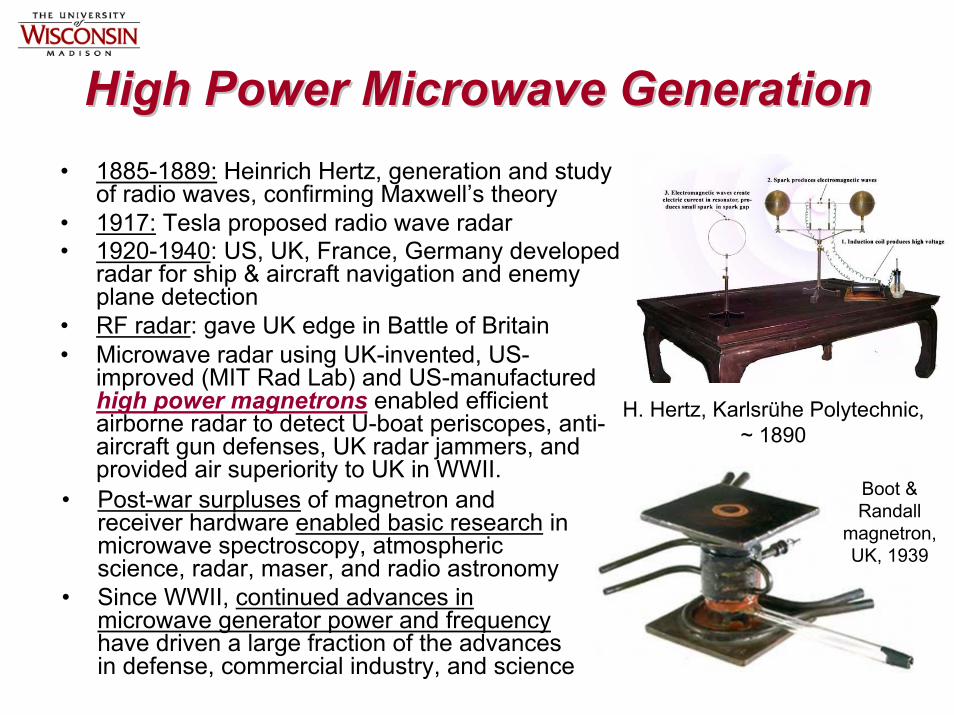
High Power Microwave GenerationHigh Power Microwave Generation• 1885-1889: Heinrich Hertz, generation and study
of radio waves, confirming Maxwell’s theory• 1917: Tesla proposed radio wave radar
H. Hertz, Karlsrühe Polytechnic, ~ 1890
• 1920-1940: US, UK, France, Germany developed radar for ship & aircraft navigation and enemy plane detection
• RF radar: gave UK edge in Battle of Britain• Microwave radar using UK-invented, US-
improved (MIT Rad Lab) and US-manufactured high power magnetrons enabled efficient airborne radar to detect U-boat periscopes, anti-aircraft gun defenses, UK radar jammers, and provided air superiority to UK in WWII.
Boot & Randall
magnetron, UK, 1939
• Post-war surpluses of magnetron and receiver hardware enabled basic research in microwave spectroscopy, atmospheric science, radar, maser, and radio astronomy
• Since WWII, continued advances in microwave generator power and frequencyhave driven a large fraction of the advances in defense, commercial industry, and science

High Power Microwave Applications (using High Power Microwave Applications (using VEDsVEDs))
Testing and instrumentationMaterials processingIndustrial plasmas, especially for semiconductor
manufacture
Industrial
Plasma heating and fusion energy researchCharged particle acceleratorsAtmospheric radarRadio astronomyMedical/BiomedicalSpectroscopyDeep space communicationsMaterials Processing researchGround Penetrating Radar
Scientific
Radar: Search, Guidance, Track, Missile-seeker, Weather, Test Electronic Counter Measures (ECM)High Power Microwave (HPM) Electronic Attack
Military
Broadcast media transmission (TV, radio)Satellite communicationsCellular (wireless) communicationsRadar, e.g.: Air traffic control, Weather, MaritimeGlobal Positioning SystemDomestic microwave cooking
Civilian infrastructure and consumer markets
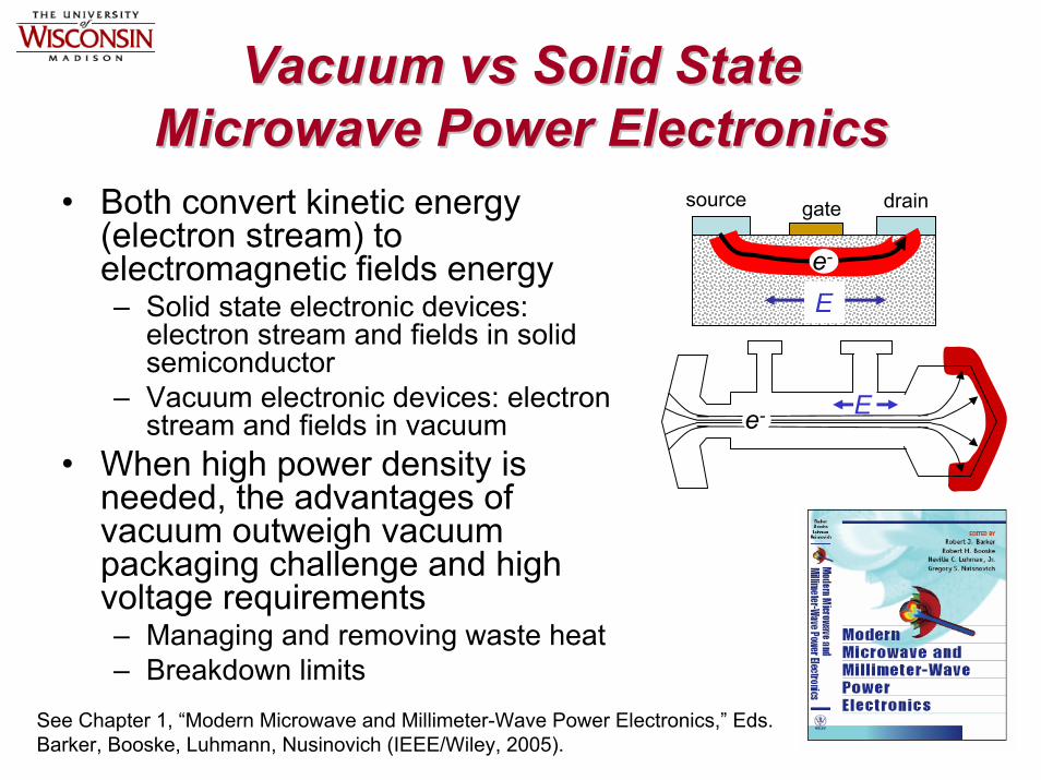
Vacuum Vacuum vsvs Solid State Solid State Microwave Power ElectronicsMicrowave Power Electronics
• Both convert kinetic energy (electron stream) to electromagnetic fields energy– Solid state electronic devices:
electron stream and fields in solid semiconductor
– Vacuum electronic devices: electron stream and fields in vacuum
• When high power density is needed, the advantages of vacuum outweigh vacuum packaging challenge and high voltage requirements – Managing and removing waste heat– Breakdown limits
See Chapter 1, “Modern Microwave and Millimeter-Wave Power Electronics,” Eds. Barker, Booske, Luhmann, Nusinovich (IEEE/Wiley, 2005).
Ee-
source draingate
e-
E

Research Frontier
101.1 100 1,000 10,000Frequency (GHz)
10 cm0.1 m 1.0 cm 1.0 mm 0.1 mm
107
106
105
104
103
102
10
1
10- 1
10- 2
10- 3
10- 4
10- 5
1011
1010
109
108
VacuumDevices
(Avg)
Vacuum HPM(Peak)
Solid State
Lasers (Peak)
Solid StateDevices (Avg)
Pow
er (W
)(S
ingl
e D
evic
es)
Electronic Attack
Plasma heating, Active Denial, Advanced Radar
Avg pwrfrontier

HPM frontier P ∝1/f 2
…BUT …
For f > 100 GHz VEDs frontier
∝ 1/f2P
High power limit for Solid State ∝ 1/f 2
andHPM
Frontier
(Single Devices)
101.1 100 1,000 10,000Frequency (GHz)
10 cm0.1 m 1.0 cm 1.0 mm 0.1 mm
107
106
105
104
103
102
10
1
10- 1
10- 2
10- 3
10- 4
10- 5
1011
1010
109
108
VacuumDevices
(Avg)
Vacuum HPM(Peak)
Solid State
Lasers (Peak)
Solid StateDevices (Avg)
Pow
er (W
)(S
ingl
e D
evic
es)
* note: does not include peak power from FELs above 100 GHz

The “THz” regime”The “THz” regime”(THz and subTHz)
Jeff. Lab
TeraView
101.1 100 1,000 10,000Frequency (GHz)
10 cm0.1 m 1.0 cm 1.0 mm 0.1 mm
107
106
105
104
103
102
10
1
10- 1
10- 2
10- 3
10- 4
10- 5
1011
1010
109
108
VacuumDevices
(Avg)
Vacuum HPM(Peak)
Solid State
Lasers (Peak)
Solid StateDevices (Avg)
Pow
er (W
)(S
ingl
e D
evic
es)
Advanced Comm, Concealed Threat Detection, Imaging, Chemistry Spectroscopy, Space, Biomedical,…

Recent vacuum Recent vacuum electronic device electronic device
breakthroughs breakthroughs towards filling the towards filling the
THz gap
NGC TWT Osc*
Jefferson Lab FEL
Novosibirsk FEL
101.1 100 1,000 10,000Frequency (GHz)
10 cm0.1 m 1.0 cm 1.0 mm 0.1 mm
107
106
105
104
103
102
10
1
10- 1
10- 2
10- 3
10- 4
10- 5
1011
1010
109
108
VacuumDevices
(Avg)
Vacuum HPM(Peak)
Solid StateDevices (Avg)
Pow
er (W
)(S
ingl
e D
evic
es)
Gyrotron(Zaytsev,
et al)
Gyrotron(Hornstein,
et al)
Gyrotron(Idehara,
et al)
THz gap
* note: does not include peak power from FELs above 100 GHz

Modified edge of Modified edge of the frontier, the frontier,
given that many given that many THz applications THz applications require require compactcompact
and and mobilemobilesources with sources with high average high average
power
10 cm0.1 m 1.0 cm 1.0 mm 0.1 mm
107
106
105
104
103
102
10
1
10- 1
10- 2
10- 3
10- 4
10- 5
1011
1010
109
108
Compact VacuumDevices (Avg)
Vacuum HPM(Peak)
Solid StateDevices (Avg)
Pow
er (W
)(S
ingl
e D
evic
es)
TWT Osc*
The The “THz” “THz” gapgap
power
101.1 100 1,000 10,000Frequency (GHz)

High Power Research FrontierHigh Power Research Frontier
• Apparently two frontiers– Constant Pf2 limit of HPM (1-100 GHz)– mmwave-to-THz, or “THz” gap (100 – 1000 GHz)
• Not so separate as they might seem: they share common “plasma physics” and related challenges of high power density:– Dense electron beams– Maximizing RF power density

ScalingScaling
(Surface) breakdown
Robust yet precise circuit fabrication
HPM: P ↑ at constant f THz: f ↑ at constant P
(10 MW)/(10 cm × 10 cm)
~ 1 MW/cm2
(100 W)/(0.1 λ0 × 0.1 λ0)
~ 1 MW/cm2 (@ 300 GHz)
High EM Power Density
Beam Impact
Beam Generation
Beam Confinement
Dense Electron Beams

High Power Density: RF BreakdownHigh Power Density: RF BreakdownNeuber, et al, Phys. Plasmas, 14, 057102 (2007)
2.85 GHz TTU
110 GHz MIT
Hidaka, et al, Phys. Rev. Lett., in review (2007)See also Poster TP8 42, Hidaka, et al, Thurs AM
• Inside the vacuum device– Arcing damage– Interrupted operation
• Outside the vacuum– Reflected radiation
• Intense E fields • Experiments
– E = f(p, τ)
– Surface & UV effects at < 10 GHz and < 300 torr (TTU)
– No UV or surface effects at 110 GHz, 760 torr but filamentationdominant (MIT)
– E ~ 20-30 kV/cm @ 760 torr(AFRL, MIT, UW, 1 GHz – UV laser)

RF Breakdown: Theoretical UnderstandingRF Breakdown: Theoretical Understanding• Vacuum
– Surface breakdown via multipactor
10
100
1000
1.E-05 1.E-04 1.E-03
P*tau (torr-s)
E/p
(V/c
m-to
rr)
TTU exptLau scaling
or field emission
– Primarily accelerator cavities
E > ~ 108 V/m
• High Pressure– Avalanche gas breakdown via
avalanche ionization
[ ] )s(
)torr(cmVτpKEeff ≈
air 1,~Kgases noble ,05.0~
K
Lau, Verboncoeur, Kim, Appl. Phys. Lett. 89, 261501 (2006)
See also, Oral Talk NO7, Wed morning, Nam, et al.
e- E
e-
e-
2v2 00 TeEmtransit ==τ & γ(Wi) > 1
e-e- e-

• Conclusions: – E for breakdown is ~ constant
with frequency, or…
• Vacuum Breakdown
• Air Breakdown
( )kV/cm 3020~
1
22
coll
0 −+
≈νω
EEeff 0
0.5
1
1 10 100 1000
frequency (GHz)
E_ef
f/E_r
ms
760 torr
2~ PfEBD– Breakdown a limiting
phenomenon for f < ~100 GHz– Breakdown is not the limiting
issue for f > ~100 GHz
Braun, et al, PRL, vol 90, 224801 (2003)
Frequency scalingFrequency scaling

High Power Density: High Power Density: THz Circuit FabricationTHz Circuit Fabrication
• Limiting phenomenon: circuit sizes required for compact generators at f > 100 GHz– rcircuit/tunnel ~ 0.1λ0 and rbeam ~ rckt/2
• For “as-designed” performance, need dimensional errors < ~ 3%[Pengvanich, et al, IEEE TED (to be published, 2008)]See also, Poster TP8 39, Pengvanich, Thursday, AM
• How to make and assemble such precise circuits with high yield?• Recent, intensive efforts to adapt MEMS microfabrication techniques
to high frequency VEDs– 3D, mechanically and thermally robust– Many approaches under investigation
• High speed micro-milling• Micro-EDM• Laser micromachining• Deep Reactive Ion Etching of Si (both circuits and molds)• Xray LIGA• UV LIGA

MicrofabMicrofab Circuit ExamplesCircuit Examples
Laser micromachinedmeanderline circuit (UW/CCR)
DRIE meanderlinecircuit (UW/CCR)
FWG made by xray LIGA (SNU)
High speed micro-milling
(SLAC/UCD)94 GHz klystron
DRIE FWG
UW’s DRIE FWGs in Si used by NGC for 670
GHz THz TWT oscillator
Si molded diamond
GenVac
• Emerging “front-runners”– Micro EDM (< 10 µm wire diameter)– Deep Reactive Ion Etching of Si

Small Circuits + High Power = Dense BeamsSmall Circuits + High Power = Dense Beams
• Reference device: 5 GHz, 100 W TWT amplifier
– 2.5 kV, 0.2 A, 20 A/cm2, rckt ~ 0.02λ0 for compact high gain & efficiency
• Scale to 200 GHz at constant voltage…λ decreases by 40 X
FE ∝ J
10
100
1000
10000
100000
1 10 100 1000
frequency (GHz)
curr
ent d
ensi
ty(A
/cm
^2)
Magnetic field focusing:22 2 pc ωω ≥
or
[ ] ( )[ ][ ]( ) 41
2
voltsA/cm
5.1kGVJ
B ≥

Scaling Challenges and OptionsScaling Challenges and Options• Scale 5 GHz, 100 W TWT amplifier to 200 GHz
– 2.5 kV, 0.2 A, 20 A/cm2, rckt ~ 0.02λ0 for compact high gain & efficiency• Bmax ~ 10 kG
r ↑ 5 XConstant V V → 20 kV
0.01
0.1
1
10
100
1 10 100 1000
frequency (GHz)
mag
netic
fiel
d (k
G)
0.1
1
10
100
1000
10000
100000
curr
ent d
ensi
ty (A
/cm
^2)
0.01
0.1
1
10
100
1 10 100 1000
frequency (GHz)
mag
netic
fiel
d (k
G)
0.1
1
10
100
1000
10000
100000
curr
ent d
ensi
ty (A
/cm
^2)
0.01
0.1
1
10
100
1 10 100 1000
frequency (GHz)
mag
netic
fiel
d (k
G)
0.1
1
10
100
1000
10000
100000
curr
ent d
ensi
ty (A
/cm
^2)
2.5 kV
20 kV
20 kV, incr r
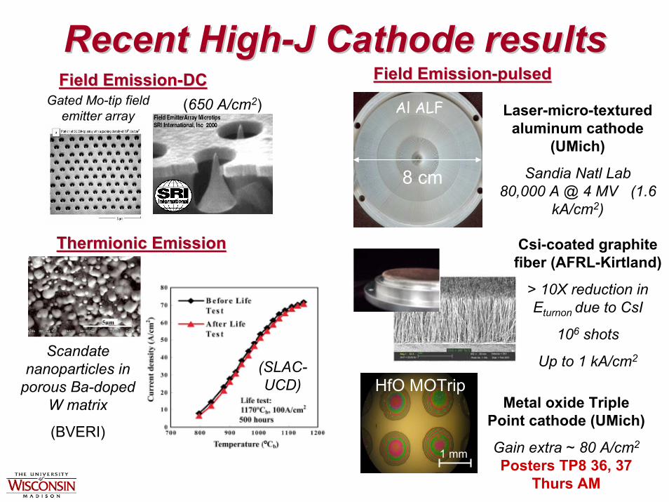
Recent HighRecent High--J Cathode resultsJ Cathode resultsField EmissionField Emission--pulsedpulsedField EmissionField Emission--DCDC
Gated Mo-tip field emitter array
(650 A/cm2)
8 cm
Al ALF Laser-micro-textured aluminum cathode
(UMich)
Sandia Natl Lab 80,000 A @ 4 MV (1.6
kA/cm2)
Thermionic EmissionThermionic Emission Csi-coated graphite fiber (AFRL-Kirtland)
> 10X reduction in Eturnon due to CsI
106 shots
Up to 1 kA/cm2Scandatenanoparticles in
porous Ba-doped W matrix
(BVERI)
(SLAC-UCD)
1 mm
HfO MOTripMetal oxide Triple
Point cathode (UMich)
Gain extra ~ 80 A/cm2
Posters TP8 36, 37 Thurs AM

Advancing cathode physics: Advancing cathode physics: Minimizing Minimizing EEturnturn--onon
Hi-res SEMCsI
C
Ab initio computational
modeling (V.A.S.P.)
CsI thin film
CsI treatment reduces Eturn-on by
10-20X
0.00 0.02 0.04 0.061
2
3
4
5
8.5 A
4.2 A (~ bulk CsI density)
16.9 A
12.7 A
Wor
k Fu
nctio
n (e
V)
Surface Coverage (molec. / A2)
bulk CsI
bulk C
21.1 A
Why it works
Ideal conditions
Vlahos, Morgan, Booske APL 91, 144102 (2007)

Advancing cathode physics:Advancing cathode physics:understanding field enhancementunderstanding field enhancement
Al PAL (UM)
500 µm
• Experimental studies [X.He, et al, Conf Proc IEEE IVNC, 2007] indicate that β~ 9-10 experimentally with ridges like these, when β~ 3 according to E-static calcs
• Recently derived the vacuum field enhancement factor for knife edge using conformal mapping*
• Asked question: what if decorated by small “invisible” features? What is net field enhancement?
• Derived result again for rectangular ridges (knife edges)
• Effect is not additive or dominated by one feature…effect is multiplicative• Confirms and proves conjecture by Schottky [(Z. Physik 14, 63,(1923)]
ah
ah
ah∝×≅
>> 4πβ
h2a
h2a
h*
2a*
**
44*
** ah
ah
ahah
ππβ ×≅>>>>>>
* Miller, Lau, and Booske, APL 91, 074105. (2007)See also, Poster TP8 38, Thursday AM

DC Dense Beam Cathode SummaryDC Dense Beam Cathode Summary• Generating dense beams, i.e., cathodes• Maximum cathode emission
– Field emission—laboratory < 650 A/cm2
– Thermionic—short life (~ 100s hrs) < 150 A/cm2
– Field emission—device < 20 A/cm2
– Thermionic—long-life (1000s hrs) < 10 A/cm2
0.01
0.1
1
10
100
1 10 100 1000
frequency (GHz)
mag
netic
fiel
d (k
G)
0.1
1
10
100
1000
10000
100000
curr
ent d
ensi
ty (A
/cm
^2)
2.5 kV
0.01
0.1
1
10
100
1 10 100 1000
frequency (GHz)
mag
netic
fiel
d (k
G)
0.1
1
10
100
1000
10000
100000
curr
ent d
ensi
ty (A
/cm
^2)
0.01
0.1
1
10
100
1 10 100 1000
frequency (GHz)
mag
netic
fiel
d (k
G)
0.1
1
10
100
1000
10000
100000
curr
ent d
ensi
ty (A
/cm
^2)
20 kV
20 kV, incr r

Advancing cathode physics: Advancing cathode physics: emission uniformityemission uniformity
• Mode competition and efficiency of vacuum electron devices are affected by the uniformity of electron beam
• High power mmwave gyrotroncathode emission is not uniform
• Two theories, both implicating mechanical machining and fabrication
• Measurements at CCR underway with new cathodes made with new diamond cutting and Ba impregnation processes
Anderson et. al , IEEE-TJensen, Lau, Jordan, APL
110 GHz, 1.5 MW gyrotron (MIT)
0
0.2
0.4
0.6
0.8
1
0 90 180 270 360Azimuthal angle (deg.)
J/Jm
ax
5kV10kV25kV70kV80 kV
MIT/CCR
ED 52, p. 825, 200588 164105 (2006)

Dense beam impact physicsDense beam impact physics
( )
,
, 4
erf4
erf,0,0,0
22
2
0
Ddt
DRt
ttdcdJVtT
zb
r
zt
rbb
==
= ∫ ττ
τρ
(assume square cross section beam for easy math)
330 A/cm2

Beam Impact: experimental illustrationBeam Impact: experimental illustration• SLAC Klystrino: 94 GHz, 1 kW klystron
– G. Scheitrum, et al, IEEE I.V.E.C. Conf Digest (2002)• 110 kV, 2.4 A, 0.25 mm radius• Magnetic focusing design had small error near output (quadrupole
leakage fields)• Beam interception at exit of circuit
– ~ 1 mm2 impact area– ~ 1 MW/cm2
– t ~ 5 µs– Exceeded single pulse damage threshold
• 3D Electron optics and magnetic design codes are better now• Superior approaches currently being pursued (…more shortly)
Courtesy, G. Scheitrum, 2007

Additional Challenge: Additional Challenge: at high frequencies, at high frequencies, space charge not the magnetic focusing limitspace charge not the magnetic focusing limit
22
2022 22 εωω
+≥au
pc
222 82makT
pc⊥+≥ ωω
orJ.D. Lawson, The Physics of Charged Particle Beams (Oxford, 1977)
• Electrons have random transverse velocities
• Magnetic field must confine both space charge and transverse “pressure gradient” defocusing forces (emittance)
• Typical well-designed VED beam has ε ~ 3 mm-mrad– Edge emission
• J.M. Finn, et al, IEEE T.P.S. 16, 281 (1988)
– Roughness • Y.Y. Lau, J.A.P. 61, 36 (1987)
• Scaled 100 W, TWT with 20 kV and max radius– kT⊥~ 5-10 eV @ 200 GHz– Single-gate FEAs, kT⊥~ 10 eV

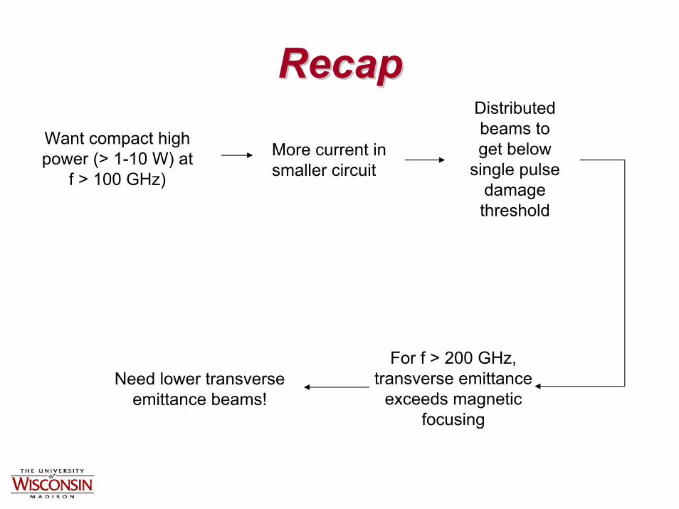
Recap: higher compact THz powerRecap: higher compact THz power
Want compact high power (> 1-10 W) at
f > 100 GHz)
More current in smaller circuit
Constant voltage ~ 3 kV
Increase V to ~ 20 kV
Magnetic focusing of space charge
OK
Need high-Jbeams
Ongoing R&D• Field emission cathodes• Thermionic cathodes
Transverse emittance exceeds magnetic focusing
rf breakdown not a concern
Beam power density
exceeds single pulse damage
threshold
Reconsider…
Space charge exceeds magnetic
focusing

Alternative: Distributed BeamsAlternative: Distributed Beams• Objective: high beam current in small (high
frequency) “circuits”• Reduce current density by spreading out beam
in one dimension, but leave other dimension small
• OptionsMultibeams Sheet Beams
• New challenge: stable beam focusing…Bz
vEXB
E

Magnetic focusing of distributed beamsMagnetic focusing of distributed beamsBasten and Booske,
J.Appl.Phys., 85, 6313 (1999)
• Or…use wiggler focusing (Booske, et al., J.A.P., 64, 6 (1988)
• Or…use solenoid focusing for short distances
• How short?...subject for additional research
• Scaling,
• High B, low beam density
2~~p
c
BE
aEBa
vat
ωω
×⊥ ∝

MultibeamsMultibeams face similar issuesface similar issues
• “Smearing” distance, zs ≤ u0t┴.• For 10 A/cm2 and 20 kV,
zs (cm) ≤ ~ 125/f(GHz)
(thickness grows more slowly)
t┴= a/vE×B
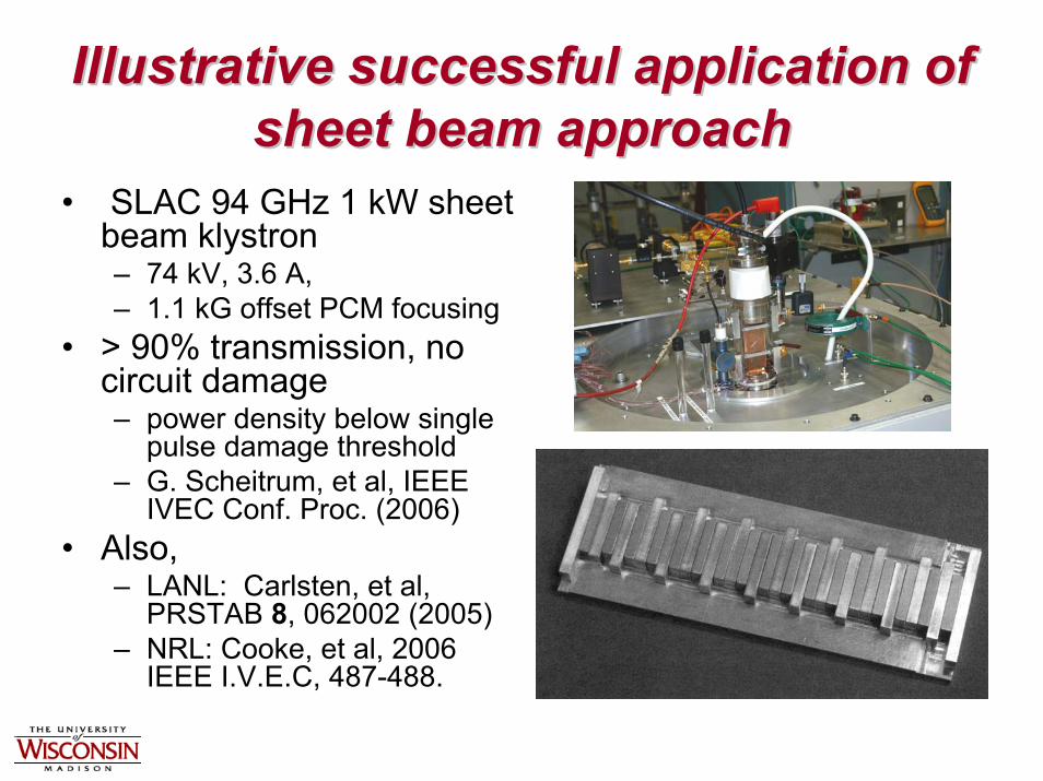
Illustrative successful application of Illustrative successful application of sheet beam approachsheet beam approach
• SLAC 94 GHz 1 kW sheet beam klystron– 74 kV, 3.6 A, – 1.1 kG offset PCM focusing
• > 90% transmission, no circuit damage– power density below single
pulse damage threshold– G. Scheitrum, et al, IEEE
IVEC Conf. Proc. (2006)• Also,
– LANL: Carlsten, et al, PRSTAB 8, 062002 (2005)
– NRL: Cooke, et al, 2006 IEEE I.V.E.C, 487-488.
RecapRecapWant compact high power (> 1-10 W) at
f > 100 GHz)
More current in smaller circuit
Distributed beams to get below
single pulse damage threshold
For f > 200 GHz, transverse emittance
exceeds magnetic focusing
Need lower transverse emittance beams!

Reducing transverse beam Reducing transverse beam emittanceemittance• Beam cooling
– Carlsten and Bishofberger, New J. Phys. 8, 286 (2006).– Only for elliptical beams and requires extra magnetic optics– 10X reduction in ε, kT┴
10 A/cm2 sheet beam
C.M. Tang, et al JVST B14, 3455 (1996)
C.A. Spindt, et al, in Vacuum Microelectronics
(Wiley, 2001)
• Advanced FEA cathodes with integral focus electrode, kT┴ ≤ 1 eV
• Meanwhile, dimensions above 200 GHz may well require microfabricated cathodes (i.e., FEAs) to reliably achieve precise dimension and alignment tolerances.

RecapRecapWant compact high power (> 1-10 W) at
f > 100 GHz)
More current in smaller circuit
Distributed beams to get below
single pulse damage threshold
For f > 200 GHz, need low emittance beams
with precise dimensional tolerances
Advanced, microfabricated field
emitter (cold) cathodes with integral focusing
Microfabricatedcircuits
success
?
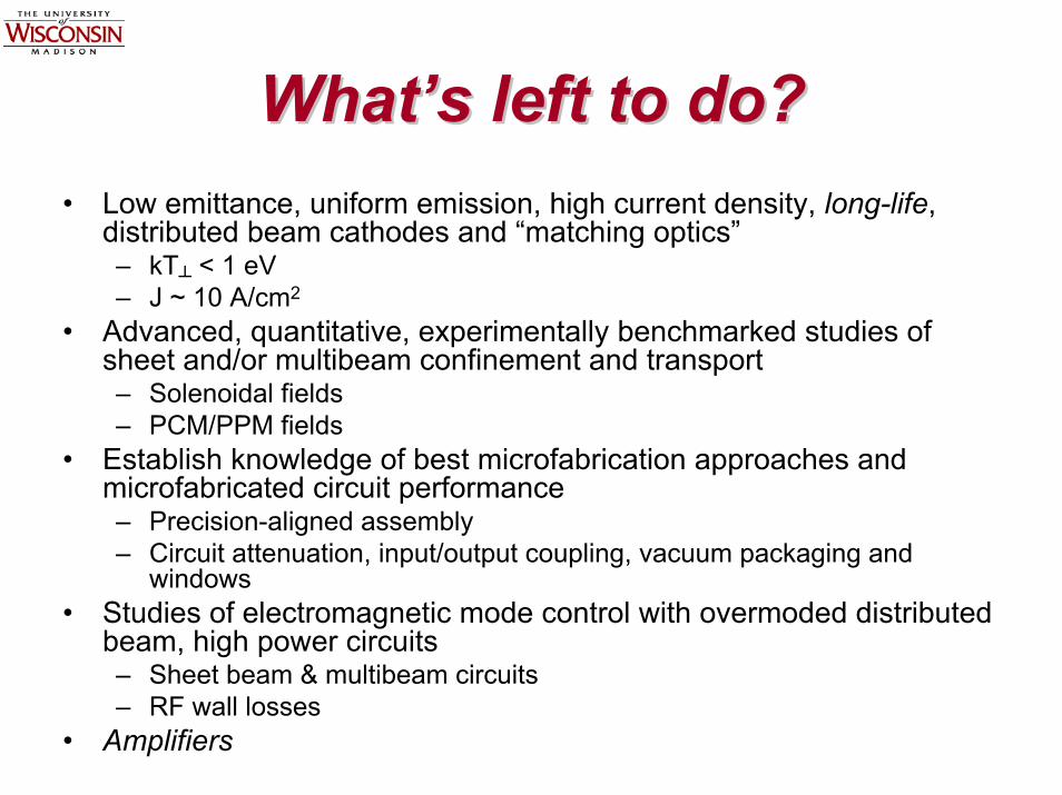
What’s left to do?What’s left to do?• Low emittance, uniform emission, high current density, long-life,
distributed beam cathodes and “matching optics”– kT┴ < 1 eV– J ~ 10 A/cm2
• Advanced, quantitative, experimentally benchmarked studies of sheet and/or multibeam confinement and transport– Solenoidal fields– PCM/PPM fields
• Establish knowledge of best microfabrication approaches and microfabricated circuit performance– Precision-aligned assembly– Circuit attenuation, input/output coupling, vacuum packaging and
windows• Studies of electromagnetic mode control with overmoded distributed
beam, high power circuits– Sheet beam & multibeam circuits– RF wall losses
• Amplifiers

Simulation toolsSimulation tools• How we’ve arrived here…
– 3D EM models (steady state and time-dependent)– 3D steady state electron optics (trajectory) codes– 3D PIC codes for time-dependent particles + EM fields– 3D thermo-mechanical models– Ab Initio surface physics models
• Persistent, aggressive, detailed benchmarking against experiments
• Persistent institutional and individual leadership and investment– U.S. Naval Research Laboratory– U.S. Air Force Office of Scientific Research/AFRL– …and many more…
[Ch. 10, in Modern Microwave and Millimeter-Wave Power Electronics (IEEE/Wiley, 2005)][Ch. 11, in High Power Microwave Sources and Technologies, Eds. Barker, Schamiloglu
(IEEE, 2001)]

SummarySummary• Vacuum electronic devices offer significant
potential for applications in the (mmwave-to)-THz regime (~ 100 - 1000 GHz) that need compact high power– Advanced communications and radar– Concealed threat detection– Imaging…
• What will it take to push back the frontier?– High power densities– High current electron beams
• Common requirements and similar challenges with HPM (< 100 GHz)– Electronic attack– RF accelerators
Recent BreakthroughsRecent Breakthroughs
• Fabrication and engineering of miniature circuits
• Understanding rf breakdown• New cathodes• Understanding cathode emission physics

Challenges at the FrontierChallenges at the Frontier• High EM power density
• HPM: delayed rf breakdown in air and vacuum• THz: mechanically and thermally robust miniature structures
• High current electron beams– Cathodes
• HPM and THz: Long life and uniform emission• THz: Low emittance beams
– Beam impact and collection• HPM: anode plasmas• HPM and THz: SEE physics, thermal engineering, materials choices
– Beam confinement• THz: Transport & magnetic focusing physics for distributed beams• THz: Cathode and device engineering for precision alignment
……In other wordsIn other words……
……there’s still a lot of fun to be had!there’s still a lot of fun to be had!

THz TWT oscillatorTHz TWT oscillator• TWT amplifier with regenerative
feedback
• Precision microfabricated circuit
• DRIE Si folded waveguide circuit
• *0.3% rf efficiency! (> 10× higher than BWOs)
• Tucek, et al, Conf Proc. IEEE IVEC 2007 (Kitakyushu, Japan)
Regenerative TWT OscillatorBWO
Bhattacharjee, Booske, vanderWeide, et al, IEEE T.P.S. 32, 1002 (2004)

State of art in compact State of art in compact mmwavemmwavedense beam focusingdense beam focusing
CPI Canada
3 kW peak
94 GHz EIK
• I ~ 0.6 A• Jcathode = 10 A/cm2
• Jbeam ~ 700 – 800 A/cm2
• V ~ 16 kV • ~ 1-10 MW/cm2 (beam power density)

Advancing cathode physics: Advancing cathode physics: understanding differences in understanding differences in JJmaxmax
• Child-Langmuir law relates J to Vanode
• 1000 A/cm2 requires – Large (!) anode voltage to extract
electrons from cathode• OK with short pulse HPM applications• Arcing with DC or long-pulse
applications
[ ] 2
2362 1033.2A/cmdVuJ −×== ρ
u
Esc
- +
0.00001
0.001
0.1
10
1000
100000
0.001 0.1 10 1000
anode voltage (kV)
curr
ent d
ensi
ty (A
/cm
^2)
d = 1 cm
1D
2D, R=10 µm– Small area cathodes (low currents
not useful for high power)
– Explains 650 A/cm2 FEA result
( )( ) R
dJJ
CL
CL
41
D1D2
+≈Y.Y. Lau, PRL 87, 278301 (2001)
Also, poster TP8 40, Ragan-Kelley, Verboncoeur