Pixel Front-End Development for CMS
8
PoS(VERTEX 2009)028 Copyright owned by the author(s) under the terms of the Creative Commons Attribution-NonCommercial-ShareAlike Licence. http://pos.sissa.it Pixel Front-End Development for CMS Beat Meier 1 Paul Scherrer Institut 5232 Villigen, Switzerland E-mail: [email protected] Jose Lazo-Flores University of Nebraska at Lincoln 5232 Villigen, Switzerland E-mail: [email protected] If the CMS pixel detector has to be replaced at the end of the lifetime there is an opportunity for a moderate upgrade. It is proposed that the upgraded detector should have 4 layers instead of three and is designed for higher luminosity and lower material budget. This proposal influences the front-end readout electronics. A higher data rate per channel is needed but the existing analog link is at the limit. Therefore it is planned to go to a low power digital serial data link. Inside the tracking area unshielded micro twisted differential pair cables with low mass will be used. To minimize dead time because of waiting for the readout an additional data buffer is included in the readout chip. This article presents the planned improvements in the readout electronics for the upgraded detector. Implementations of ASIC test structures of the critical components already exist and the first results from the measurements are also presented. VERTEX 2009 (18 th workshop) – VERTEX 2009 Veluwe, the Netherlands September 13-18, 2009 1 Speaker
Transcript of Pixel Front-End Development for CMS

PoS(VERTEX 2009)028
Copyright owned by the author(s) under the terms of the Creative Commons Attribution-NonCommercial-ShareAlike Licence. http://pos.sissa.it
Pixel Front-End Development for CMS
Beat Meier1 Paul Scherrer Institut 5232 Villigen, Switzerland E-mail: [email protected]
Jose Lazo-Flores University of Nebraska at Lincoln 5232 Villigen, Switzerland E-mail: [email protected]
If the CMS pixel detector has to be replaced at the end of the lifetime there is an opportunity for a moderate upgrade. It is proposed that the upgraded detector should have 4 layers instead of three and is designed for higher luminosity and lower material budget. This proposal influences the front-end readout electronics. A higher data rate per channel is needed but the existing analog link is at the limit. Therefore it is planned to go to a low power digital serial data link. Inside the tracking area unshielded micro twisted differential pair cables with low mass will be used. To minimize dead time because of waiting for the readout an additional data buffer is included in the readout chip. This article presents the planned improvements in the readout electronics for the upgraded detector. Implementations of ASIC test structures of the critical components already exist and the first results from the measurements are also presented.
VERTEX 2009 (18th workshop) – VERTEX 2009 Veluwe, the Netherlands September 13-18, 2009
1 Speaker

PoS(VERTEX 2009)028
CMS Pixel developments Beat Meier
2
1. Description of the current Detector and Readout
1.1 CMS Pixel Detector
The pixel detector is the innermost part of the tracking system of the CMS detector. It consists of the central part, referred to as the barrel, and a forward part at each end. The detector is divided in two shells, which come together around the beam pipe (see Figure 1 & 2). The supply tubes are located on both ends of the barrel part along the beam pipe. The forward part is located inside the supply tubes close to the barrel. For more information about the CMS pixel detector see [1], subsection “Pixel Detector”.
1.2 Layout and Cabling
The barrel pixel detector consists of 720 detector modules (see Figure 3). There are two types of detector modules, full modules and half modules. A full module can handle 16 readout chips (ROCs) and half modules handle 8 ROCs. Half modules are counted here as 0.5 modules in the total number of detector modules. The forward pixel has a completely different structure
and consists of blades of different sizes but the readout electronic is the same.
The token bit manager (TBM) on a detector module is responsible for the readout and distributes the signals to the 16 ROCs. Each module is connected with two cables to the end-flange printed circuit board (PCB). All cables have individual length depending on the
module’s position. One cable consists of a copper clad aluminum ribbon used to power the electronics and to provide bias voltage to the sensors. The other cable is a Kapton® flat band cable used for the signals. The signals are the clock, trigger, data line to configure the detector modules, and the data uplink for module readout. Each module of the outermost layer has one
Figure 2. Forward pixel detector
Figure 1. Barrel pixel detector with supply tube in front and back
Figure 3. Shown here is the barrel pixel detector module with Kapton® cable. The ribbon cable for the power is not visible here. The TBM is the part in the middle.
PoS(VERTEX 2009)028
CMS Pixel developments Beat Meier
3
data uplink and the modules of the middle and the innermost layer have two data uplinks each. This is due to the higher data rate for the inner layers. The end flange PCBs are connected to the supply tube where the optical hybrids for the different signals are placed. Each uplink ends in an optical fiber on the supply tube.
The data uplink runs at 40 MHz and consists of a multilevel signal to code the pixel address information and an analog signal for the pulse height information. The whole signal chain is analog, including the optical signal. Therefore, linear amplifiers are needed whose bandwidth is limited.
2. Requirements for the Upgrade
The goal for the upgrade is to have lower mass in the sensitive tracking area with a new mechanical structure and CO2 cooling. It is proposed to go to a four-layer barrel detector and to add a third disk to the forward detector on both sides. The upgraded detector should be designed for double the luminosity, which has consequences for the front-end electronics and the module cabling. The plan is to fulfill the requirements with minimal changes.
2.1 New Detector Layout and Cabling
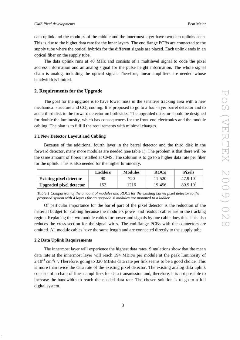
Because of the additional fourth layer in the barrel detector and the third disk in the forward detector, many more modules are needed (see table 1). The problem is that there will be the same amount of fibers installed at CMS. The solution is to go to a higher data rate per fiber for the uplink. This is also needed for the higher luminosity.
Ladders Modules ROCs Pixels Existing pixel detector 90 720 11’520 47.9·106 Upgraded pixel detector 152 1216 19’456 80.9·106
Table 1 Comparison of the amount of modules and ROCs for the existing barrel pixel detector to the proposed system with 4 layers for an upgrade. 8 modules are mounted to a ladder.
Of particular importance for the barrel part of the pixel detector is the reduction of the material budget for cabling because the module’s power and readout cables are in the tracking region. Replacing the two module cables for power and signals by one cable does this. This also reduces the cross-section for the signal wires. The end-flange PCBs with the connectors are omitted. All module cables have the same length and are connected directly to the supply tube.
2.2 Data Uplink Requirements
The innermost layer will experience the highest data rates. Simulations show that the mean data rate at the innermost layer will reach 194 MBit/s per module at the peak luminosity of 2·1034 cm-2s-1. Therefore, going to 320 MBit/s data rate per link seems to be a good choice. This is more than twice the data rate of the existing pixel detector. The existing analog data uplink consists of a chain of linear amplifiers for data transmission and, therefore, it is not possible to increase the bandwidth to reach the needed data rate. The chosen solution is to go to a full digital system.

PoS(VERTEX 2009)028
CMS Pixel developments Beat Meier
4
A low mass cable has to be found for cabling the 1216 modules. The needed cable length is 1 meter. In order to make the choice of the type of wire to use and the logic levels, we had to optimize for low mass and low power at 320 MBit/s. An unshielded micro-twisted pair cable with 125 µm wire diameter fits best. A differential transmitter and receiver with small levels for low power consumption had to be designed. For more information see [2].
3. The new Digital Module
All electrical design changes affect only the data readout. Figure 4 shows an overview of the module readout. The ROC has new fully digital outputs that are connected to a bus with a speed of 160 MBit/s. In the TBM only the analog part will be replaced by a digital multiplexer where two of this busses are combined to the 320 MBit/s data uplink. This is simply done by multiplexing the two input data streams (channel A & B) bitwise. Channel B is sent inverted so that the two channels can be separated at the receiver end and to have enough signal edges for clock and data recovery.
3.1 New ROC Architecture and Data Loss
Different algorithms, like zero suppression, are implemented in the readout chip. This is absolutely essential to handle the amount of data of the pixel detector. Buffers in the ROC reduce the resulting data rate fluctuations. However, buffer overflows cannot be excluded. For higher data rate we have to increase the buffer sizes. Figure 5 shows an overview of the readout mechanism of the proposed system. Also, the simulated peak data loss, in percent, for the different components is shown. Compared to the old system, the buffer sizes in the column interface have changed and a readout buffer is added. This buffer decouples the column readout from the external readout. In this way, the data buffers in the double columns can be cleared immediately by copying the data to the readout buffer. Because, the double columns have not to wait for the external readout token, this data loss can be limited to 2.2%. The double column interface that has to copy the pixels with a hit reaches 2% inefficiency. These values are calculated for the modules with the highest data rate at the innermost layer.
ROC
AOH320 Mbit/s up link
1m twisted pairMU
X
Token A
Token B
TBM
ROC ROC ROCROC ROC ROC ROC ROC
ROC ROC ROCROC ROC ROC ROC ROC
160 Mbit/s Bus Channel B
160 Mbit/s Bus Channel A
Figure 4 Block diagram of the digital module readout architecture.

PoS(VERTEX 2009)028
CMS Pixel developments Beat Meier
5
3.2 Buffer Modifications in the ROC
The sizes of the buffers in the column interface of the ROC have to be increased as shown in figure 5. This implies a longer readout chip. Because of mechanical constraints, the length of the chip can only be increased by 800 µm. So, it is not possible to implement the proposed buffer sizes. But it is possible to reduce the memory cell size. In this way the pitch can be reduced from 36 µm to less than 24 µm. With this modification, the memory fits in the chip and there is even an extra space for the readout buffer.
3.3 New digital Readout Architecture of the ROC
The new digital readout can be implemented in the ROC interface block. The column buffer mechanism is the same, therefore, only the buffer size changes. The pixel row and column information is already digitally. Only the pulse height has to be digitized. For this, an 8 Bit successive approximation ADC is proposed (see Figure 6). To have enough data throughput with one ADC per ROC, the ADC has to run with 80 MHz clock frequency.
The readout is initiated with an external token. For the existing system, the token is directly sent to the column interfaces. For the new system, the column and the ROC readouts are separated which is done by adding a separate token controller and readout buffer. Data are then internally grouped in four parallel bits. To send the data to the bus a four bit serializer and a differential driver are needed. In this way most of the logic can run at 40 MHz clock frequency except the ADC, running at 80 MHz, and the serializer and driver, both running at 160 MHz. To generate these clock frequencies at a multiple of the LHC clock frequency a PLL is needed.
Figure 5 Data loss in the new ROC (red numbers) with increased buffer sizes in the double columns and the new readout buffer. The buffer sizes of the existing mechanism are in brackets

PoS(VERTEX 2009)028
CMS Pixel developments Beat Meier
6
4. Test of the Critical Components
Most of the changes can be designed with standard logic cells running at 40 MHz. The critical components are already implemented in ASIC test structures. These are the 8 bit ADC, the PLL clock multiplier, and the 160/320 MBit/s transmitter and receiver respectively.
4.1 PLL Frequency Multiplier
Figure 7 shows the block diagram and Figure 8 the layout of the PLL clock multiplier. It generates the 80 MHz for the ADC and the 160 MHz for the serializer. No external components, i.e. capacitors, are needed.
PFD
Loop Filter
LHC Clock40 MHz
160 MHzserial clock
&
UP
DOWN
Charge Pump
current adjust
50pF
4.4k 3pF
4.4kVCO
VCO bias adjust
7 stage ring oscillator
80 MHzADC clock
D Q
R
1
D Q
R
1:2
:2
Figure 7 Block diagram of the frequency multiplier PLL. (PFD = phase frequency detector)
token control
Token In Token Out
DCOL token
sequencer
40 MHz Clock
ROC Control Interface Block160 MHz80 MHz
40 MHz
Pixel Address15 bit digital
Pulse Heightanalog
PLLclock distribution
160 Mbit/s data bus
23 bit
4 bit serializertoken control MUX
26 double column data buffer
8 bit SAR-ADC
readout buffer
Figure 6 Building blocks in the ROC periphery for the new buffered digital readout logic. To digitize the analog pulse height information an ADC is needed. Most of the Logic works at 40 MHz except the ADC (80 MHz), the serializer and the driver (160 MHz)

PoS(VERTEX 2009)028
CMS Pixel developments Beat Meier
7
The PLL locks to an input frequency in the range from 10 to 75 MHz and is stable in 3 µs
(see Figure 9). A supply current of only 720 µA is measured.
4.2 8-bit Analog to Digital Converter
The ADC is a current coupled 8 bit successive approximation ADC with a sample and hold included. It needs eight clock cycles for a conversion. The implementation on the ASIC test structure seems to work but is too slow. The problem is with the comparator, which is three times slower than previous simulations have shown. For the next design iteration, the comparator has to be optimized.
4.3 Electrical Low Power Data Link
To test the performance of the digital link, a test setup is built consisting of a driver, micro-twisted cable, and a receiver. The link is tested with different cable length and signal amplitudes. Also, different common mode voltage differences between driver and receiver are applied. The signal quality for a nominal signal level of 40 mV (+/- 20 mV) at different cable length is shown in Figure 10.
Measurements under different conditions show that the bit error rate is below 10-12 at a cable length of 1 m and at nominal and minimal differential signal levels down to 20 mV. Crosstalk is -27 dB to a parallel wire. The total power consumption for a link is 4 mW. This
loop filter
PFD charge pump
VCO
:4
driver
bypass filter caps
350 um10
0 um
Figure 8 Layout of the full monolithic frequency multiplier PLL.
Figure 9 Phase of the 160 MHz output at power up. The PLL is stable in 3 µs.

PoS(VERTEX 2009)028
CMS Pixel developments Beat Meier
8
power consists of the power for the transmitter and receiver. More EMI tests have to be made with higher number of cables and modules.
4.4 Implementation in the New ROC
The control interface block (CIB) is located at the bottom of the chip. Here are also located the wire bond pads, voltage regulators, DACs, communications controller and much more. This is the best place to implement the new design blocks for the digital readout. There is some empty space left to place the ADC, the serializer and the PLL (see Figure 11). The token controller and sequencer replace the old logic. Therefore it is not needed to move other blocks in the ROC. The wire bond pad assignment will be the same. The readout buffer can be placed just above the CIB and below the pixel array with the column interface.
5. Conclusion
The requirements of material budget reduction, higher data rate handling and using the existing data readout infrastructure have given rises a series of problems for the upgrade of the pixel detector. The desire to add a fourth layer to the barrel part and a third disk to the forward parts also adds to the infrastructure limitations. The solution with minimal effort is to go to digital data links at 320MBit/s and to increase the buffer sizes. The needed critical building blocks (ADC, PLL, line drivers/receivers) for the new readout are designed and tested.
References
[1] CMS Collaboration, The CMS experiment at the CERN LHC, 2008 JINST 3 S08004
[2] B. Meier, Design Studies of a Low Power Serial Data Link for a possible Upgrade of the CMS Pixel Detector, proceeding of TWEPP 2008 workshop.
Figure 10 Eye pattern of the signal at the receiver side with different cable length at 320 Mbit/s and a differential driver level of 40 mV. The planned length for the new detector is 1m.
ROCROC
8 bit ADC PLLserializerLogic
Figure 11 The small part of the ROC layout of the interface block (see red mark left) where the implementation of the digital logic is planned.
