Pipelining & Verilog - Faculty Personal Homepage-...
11
Lab #3 due tonight, LPSet 8 Thurs 10/11 Pipelining & Verilog • Latency & Throughput • Pipelining to increase throughput • Retiming Retiming • Verilog Math Functions • Debugging Hints 1 Lecture 9 6.111 Fall 2012 Sequential Divider Assume the Dividend (A) and the divisor (B) have N bits. If we only want to invest in a single N-bit adder, we can build a sequential circuit that processes a single subtraction at a time and then cycle the circuit N times. This circuit works on unsigned operands; for signed operands one can remember the signs, make operands positive, then correct sign of result. Init: P0, load A and B Repeat N times { B P A S N+1 N+1 Repeat N times { shift P/A left one bit temp = P-B if (temp > 0) N bits LSB 0 S 0 1 - N+1 N+1 N+1 {Ptemp, A LSB 1} else A LSB 0 } Done: Q in A, R in P >0? S Lecture 9 2 6.111 Fall 2012 Verilog divider.v 6.111 Fall 2012 Lecture 9 3 L. Williams MIT ‘13 Math Functions in Coregen Wide selection of math functions available 4 Lecture 9 6.111 Fall 2012
Transcript of Pipelining & Verilog - Faculty Personal Homepage-...
Lab #3 due tonight, LPSet 8 Thurs 10/11
Pipelining & Verilog• Latency & Throughput• Pipelining to increase throughput• RetimingRetiming• Verilog Math Functions• Debugging Hints
1Lecture 96.111 Fall 2012
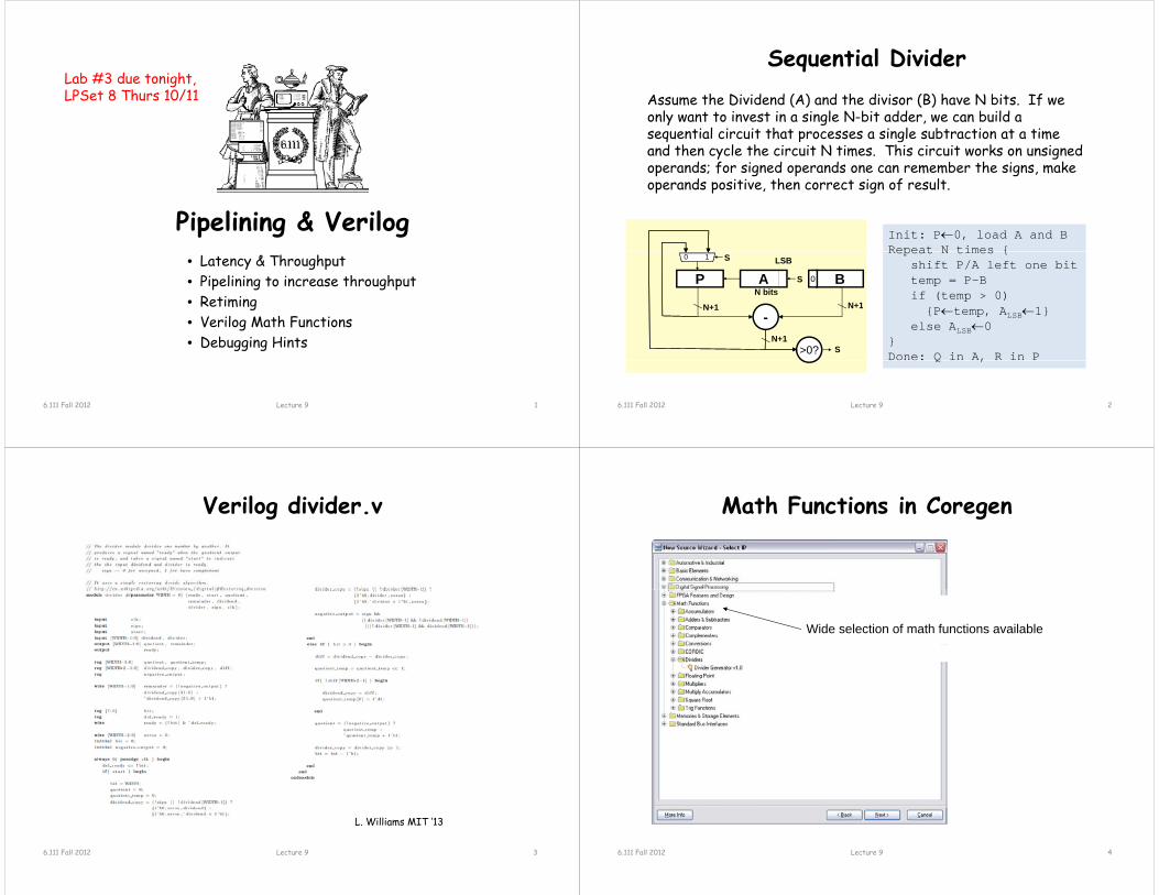
Sequential DividerAssume the Dividend (A) and the divisor (B) have N bits. If we only want to invest in a single N-bit adder, we can build a sequential circuit that processes a single subtraction at a time pand then cycle the circuit N times. This circuit works on unsigned operands; for signed operands one can remember the signs, make operands positive, then correct sign of result.
Init: P0, load A and BRepeat N times {
BP A S
N+1N+1
Repeat N times {shift P/A left one bittemp = P-Bif (temp > 0)N bits
LSB
0
S0 1
-N+1N+1
N+1
{Ptemp, ALSB1}else ALSB0
}Done: Q in A, R in P>0? S
Lecture 9 2
Q ,
6.111 Fall 2012
Verilog divider.v
6.111 Fall 2012 Lecture 9 3
L. Williams MIT ‘13
Math Functions in Coregen
Wide selection of math functions available
4Lecture 96.111 Fall 2012
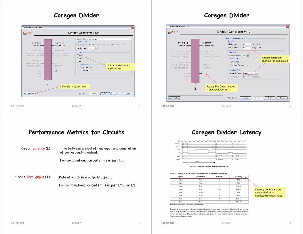
Coregen Divider
not necessary manynot necessary many applications
Details in data sheet.
6.111 Fall 2012 5Lecture 9Lecture 9 56.111 Fall 2012
Coregen Divider
Chose minimium number for application
Ready For Data: needed if clocks/divide >1
6.111 Fall 2012 6Lecture 9Lecture 9 66.111 Fall 2012
Performance Metrics for Circuits
time between arrival of new input and generation of corresponding output.
Circuit Latency (L):p g p
For combinational circuits this is just tPD.
Rate at which new outputs appear.Circuit Throughput (T):
For combinational circuits this is just 1/tPD or 1/L.
6.111 Fall 2012 7Lecture 9Lecture 9 76.111 Fall 2012
Coregen Divider Latency
Latency dependent on dividend width + fractioanl reminder width
6.111 Fall 2012 8Lecture 9Lecture 9 86.111 Fall 2012
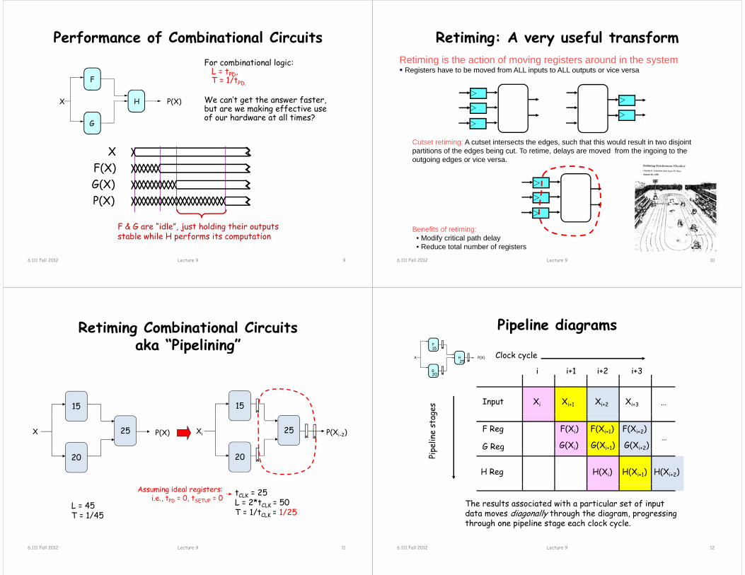
Performance of Combinational Circuits
F
For combinational logic:L = tPD, T = 1/tPD.
G
HX P(X) We can’t get the answer faster, but are we making effective use of our hardware at all times?
X
G(X)F(X)
P(X)P(X)
F & G are “idle”, just holding their outputs jstable while H performs its computation
9Lecture 96.111 Fall 2012
R ti i i th ti f i i t d i th t
Retiming: A very useful transformRetiming is the action of moving registers around in the system Registers have to be moved from ALL inputs to ALL outputs or vice versa
Cutset retiming: A cutset intersects the edges, such that this would result in two disjoint partitions of the edges being cut. To retime, delays are moved from the ingoing to the outgoing edges or vice versa.outgoing edges or vice versa.
Benefits of retiming:Benefits of retiming:• Modify critical path delay• Reduce total number of registers
10Lecture 96.111 Fall 2012
Retiming Combinational Circuitsaka “Pipelining”aka Pipelining
15 15
P(X)25X P(Xi-2)25Xi
20 20
L = 45T = 1/45
tCLK = 25L = 2*tCLK = 50T = 1/tCLK = 1/25
Assuming ideal registers:i.e., tPD = 0, tSETUP = 0
11Lecture 96.111 Fall 2012
Pipeline diagramsF
i i+1 i+2 i+3
Clock cycleF
G
HX P(X)
15
20
25
Input Xi Xi+1 Xi+2 Xi+3
ges …
F Reg
G Reg
F(Xi)
G(Xi)
F(Xi+1)
G(Xi+1)
F(Xi+2)
G(Xi+2)pelin
e st
ag…
G Reg
H Reg
( i) ( i+1)
H(Xi)
( i+2)
H(Xi+1)
Pip
H(Xi+2)
The results associated with a particular set of input data moves diagonally through the diagram, progressing through one pipeline stage each clock cycle.
12Lecture 96.111 Fall 2012

Pipeline ConventionsDEFINITION:
a K-Stage Pipeline (“K-pipeline”) is an acyclic circuit having exactly K registers on every path from an input to an output.
a COMBINATIONAL CIRCUIT is thus an 0-stage pipeline.
CONVENTION:Every pipeline stage, hence every K-Stage pipeline, has a register on its Every pipeline stage, hence every K Stage pipeline, has a register on its OUTPUT (not on its input).
ALWAYS:The CLOCK common to all registers must have a period sufficient to The CLOCK common to all registers must have a period sufficient to cover propagation over combinational paths PLUS (input) register tPDPLUS (output) register tSETUP.
The LATENCY of a K-pipeline is K times the period of the clock common to all registers.
The THROUGHPUT of a K-pipeline is the frequency of the clock.
13Lecture 96.111 Fall 2012
Ill-formed pipelines
A
Consider a BAD job of pipelining:
21CX A 21
BY
Problem:
noneFor what value of K is the following circuit a K-Pipeline? ________
Successive inputs get mixed: e.g., B(A(Xi+1), Yi). This happened because some paths from inputs to outputs have 2 registers, and some have only 1!This CAN’T HAPPEN on a well-formed K pipeline!
14Lecture 96.111 Fall 2012
A pipelining methodologyStep 1:Add a register on each output.
STRATEGY:Focus your attention on placing pipelining registers
Step 2:Add another register on each output Draw a cut-set contour
around the slowest circuit elements (BOTTLENECKS).
output. Draw a cut set contour that includes all the new registers and some part of the circuit. Retime by moving regs A B Cy g gfrom all outputs to all inputs of cut-set.
4 nS 3 nS 8 nS
D4 nS
F5 nS
Repeat until satisfied with T. E2 nS
T = 1/8nsL = 24ns
15Lecture 96.111 Fall 2012
Pipeline Example
A CX2 1
OBSERVATIONS:• 1-pipeline improves
12 3
BY
2
1
1 1 pipeline improves neither L or T.
• T improved by breaking long combinational paths, ll f l k
2 3
1
LATENCY THROUGHPUT
allowing faster clock.• Too many stages cost L,
don’t improve T.
0-pipe:L E
4 1/4• Back-to-back registers
are often required to keep pipeline well-formed.1-pipe: 4 1/4
2-pipe: 4 1/2
3-pipe: 1/26 1/2
16Lecture 96.111 Fall 2012
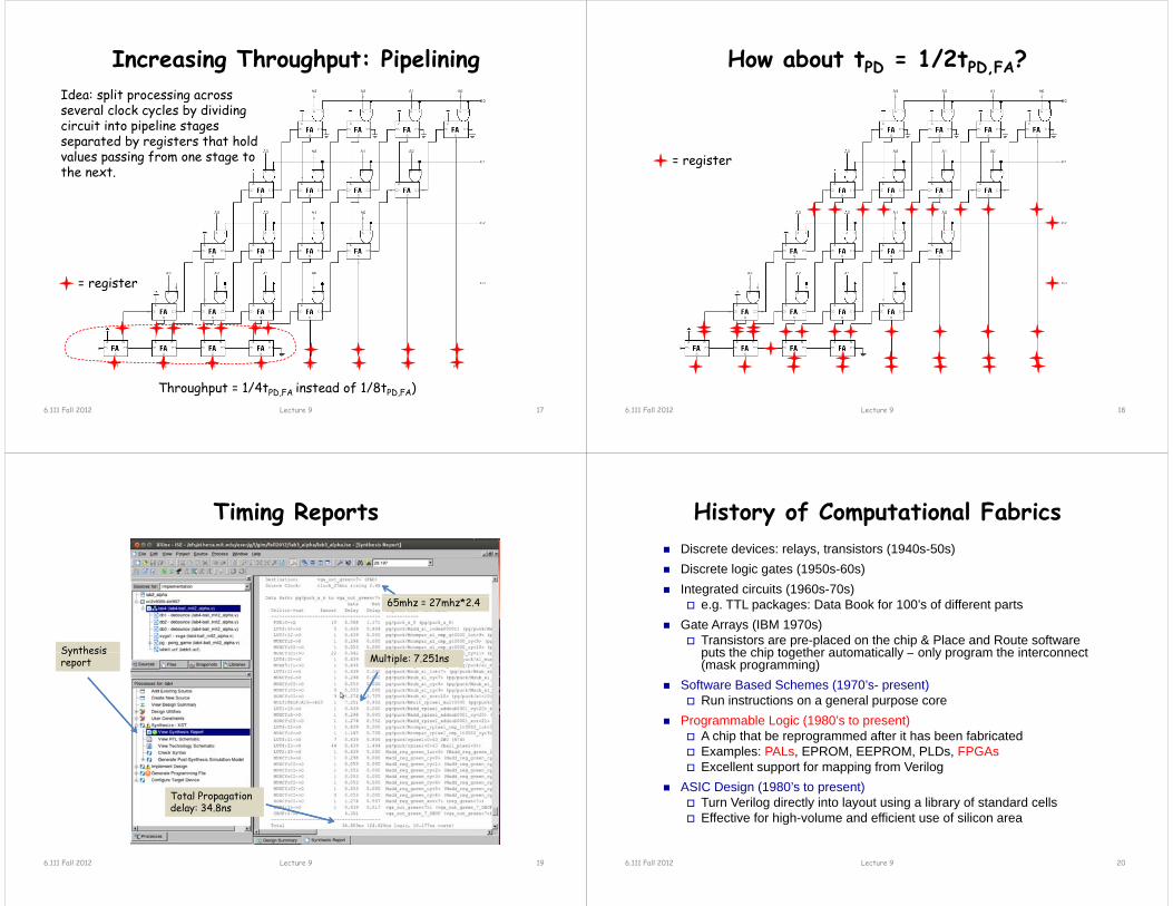
Increasing Throughput: Pipelining l Idea: split processing across
several clock cycles by dividing circuit into pipeline stages separated by registers that hold separated by registers that hold values passing from one stage to the next.
= register
Throughput = 1/4tPD,FA instead of 1/8tPD,FA)17Lecture 96.111 Fall 2012
How about tPD = 1/2tPD,FA?
= register
Lecture 9 186.111 Fall 2012
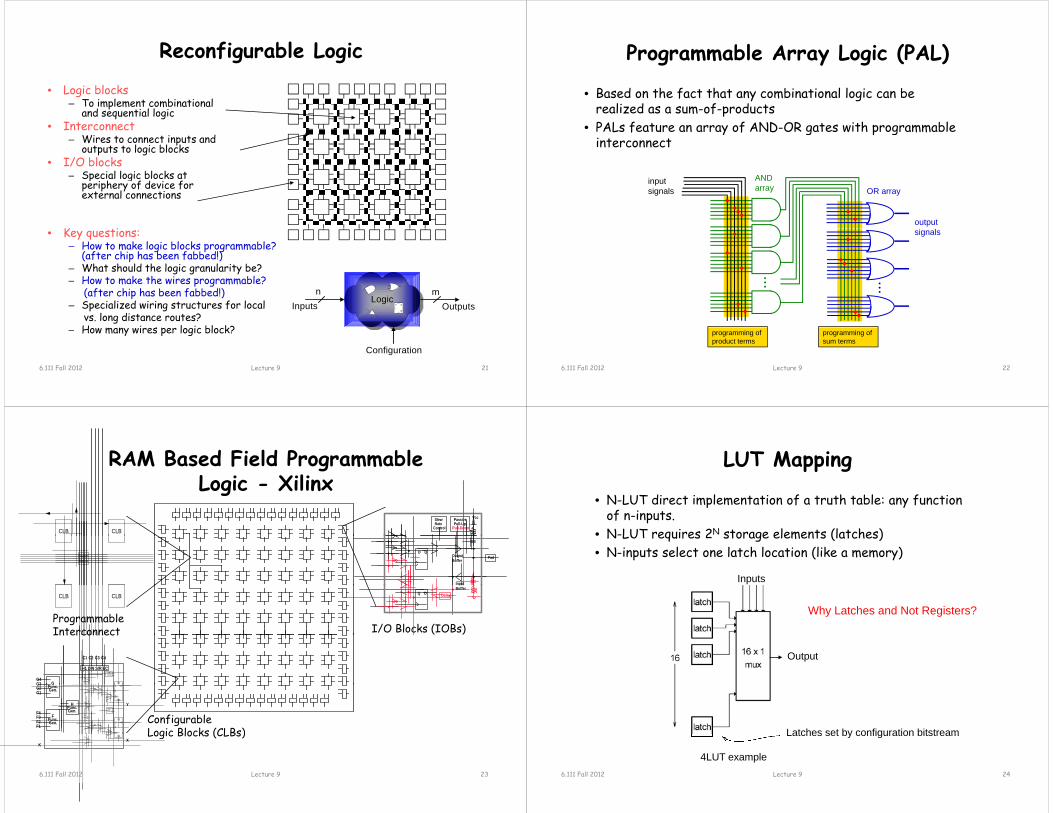
Timing Reports
65mhz = 27mhz*2.4
Synthesis Multiple: 7.251ns
Synthesis report
Total Propagation delay: 34.8ns
Lecture 9 196.111 Fall 2012
History of Computational Fabrics Discrete devices: relays, transistors (1940s-50s) Discrete logic gates (1950s-60s) Integrated circuits (1960s-70s)
e.g. TTL packages: Data Book for 100’s of different parts Gate Arrays (IBM 1970s)
Transistors are pre-placed on the chip & Place and Route software puts the chip together automatically only program the interconnectputs the chip together automatically – only program the interconnect (mask programming)
Software Based Schemes (1970’s- present) Run instructions on a general purpose core
Programmable Logic (1980’s to present) A chip that be reprogrammed after it has been fabricated Examples: PALs, EPROM, EEPROM, PLDs, FPGAs
E ll t t f i f V il Excellent support for mapping from Verilog ASIC Design (1980’s to present)
Turn Verilog directly into layout using a library of standard cells Effective for high volume and efficient use of silicon area Effective for high-volume and efficient use of silicon area
Lecture 9 206.111 Fall 2012
Reconfigurable Logic
• Logic blocks– To implement combinational
and sequential logic• InterconnectInterconnect
– Wires to connect inputs andoutputs to logic blocks
• I/O blocks– Special logic blocks at Sp c a og c oc s at
periphery of device forexternal connections
K i• Key questions:– How to make logic blocks programmable?
(after chip has been fabbed!)– What should the logic granularity be?
H t k th i bl ?– How to make the wires programmable?(after chip has been fabbed!)
– Specialized wiring structures for localvs. long distance routes?H i s l i bl k?
LogicLogicInputs Outputs
n m
Q
QSET
CLR
D
– How many wires per logic block?
Configuration
Lecture 9 216.111 Fall 2012
Programmable Array Logic (PAL)
• Based on the fact that any combinational logic can be realized as a sum-of-products
• PALs feature an array of AND-OR gates with programmable PALs feature an array of AND OR gates with programmable interconnect
i t ANDinputsignals
output
ANDarray OR array
signals
programming of product terms
programming of sum terms
Lecture 9 226.111 Fall 2012
RAM Based Field Programmable Logic - XilinxLogic Xilinx
CLB CLB
SlewRate
Control
PassivePull-Up,
Pull-Down
Vcc
SwitchMatrix
D QOutputBuffer
Input
Pad
CLB CLB
ProgrammableInterconnect I/O Blocks (IOBs)
Delay
pBuffer
Q D
Interconnect
SD
S/RControl
F'DING
G4G3
C4C1 C2 C3
H1 DIN S/R EC
ConfigurableLogic Blocks (CLBs)
D Q
RDEC
D QSD
EC
S/RControl
1
F'G'
H'
DIN
FG'
H'
G'H'
HFunc.Gen.
GFunc.Gen.
FFunc.Gen.
G3G2G1
F4F3F2F1
Y
Logic Blocks (CLBs)RD1
F'
H'
KX
Lecture 9 236.111 Fall 2012
LUT Mapping
• N-LUT direct implementation of a truth table: any function of n-inputs.
• N-LUT requires 2N storage elements (latches)N LUT requires 2 storage elements (latches)• N-inputs select one latch location (like a memory)
Inputs
Why Latches and Not Registers?
Output
Latches set by configuration bitstream
4LUT example
Latches set by configuration bitstream
Lecture 9 246.111 Fall 2012
Configuring the CLB as a RAM
Memory is built using Latches not FFs
16x2
Read is same a LUT Function!Lecture 9 256.111 Fall 2012
Xilinx 4000 Interconnect
Lecture 9 266.111 Fall 2012
Xilinx 4000 Interconnect Details
Wires are not ideal!
Lecture 9 276.111 Fall 2012
Add Bells & Whistles
HardProcessor
Gigabit Serial
I/O
Serial
18 Bit36 Bit
Multiplier
ZZZ ImpedanceControl
18 Bit
BRAM
ProgrammableTermination
ZZZ ImpedanceControl
ClockMgmt
Courtesy of David B. Parlour, ISSCC 2004 Tutorial, “The Reality and Promise of Reconfigurable Computing in Digital Signal Processing”
Lecture 9 286.111 Fall 2012

The Virtex II CLB (Half Slice Shown)
Lecture 9 296.111 Fall 2012
Adder ImplementationCout
LUT: AB
Y = A B CinAB
Dedicated carry logic
1 half-Slice = 1-bit adder
Dedicated carry logic
Cin
Lecture 9 306.111 Fall 2012
Virtex-6
DSP with 25x18 multiplier
Gigabit ethernet
CLB Dist RAM Block RAM Multipliers
Gigabit ethernet support
Virtex 2 8,448 1,056kbit 2,592kbit 144 (18x18)Virtex 6 667,000 6,200kbit 22,752kbit 1,344 (25x18)Spartan 3E 240 15kbit 72kbit 4 (18x18)
Lecture 9 316.111 Fall 2012
Design Flow - Mapping
• Technology Mapping: Schematic/HDL to Physical Logic units• Compile functions into basic LUT-based groups (function of
target architecture)target architecture)
ac
Q
QSET
CLR
D
LUTQ
QSET
CLR
Dbc
db
always @(posedge clock or negedge reset)begin
if (! t)if (! reset)q <= 0;
elseq <= (a & b & c) | (b & d);
end
Lecture 9 326.111 Fall 2012

Design Flow – Placement & RoutePl i l i l i i l d i • Placement – assign logic location on a particular device
LUT
LUT
LUT
Routing – iterative process to connect CLB inputs/outputs and IOBs. Optimizes critical path delay – can take hours or days for large, dense designs
Iterate placement if timing not met
Satisfy timing? Generate Bitstream to config device
Challenge! Cannot use full chip for reasonable speeds (wires are not ideal).
Typically no more than 50% utilization.Lecture 9 336.111 Fall 2012
Example: Verilog to FPGA
module adder64 ( • Synthesismodule adder64 ( input [63:0] a, b; output [63:0] sum);
assign sum = a + b;
• Synthesis• Tech Map• Place&Route
assign sum = a + b;endmodule
Virtex II XC2V200064-bit Adder Example Virtex II – XC2V200064 bit Adder Example
Lecture 9 346.111 Fall 2012
How are FPGAs Used?
Logic Emulation Prototyping
Ensemble of gate arrays used to emulate a Ensemble of gate arrays used to emulate a circuit to be manufactured
Get more/better/faster debugging done than with simulation
Reconfigurable hardware One hardware block used to implement more
than one function
Special-purpose computation engines Hardware dedicated to solving one problem
(or class of problems) Accelerators attached to general-purpose
FPGA-based Emulator
Accelerators attached to general-purpose computers (e.g., in a cell phone!)
(courtesy of IKOS)FPGA based Emulator
Lecture 9 356.111 Fall 2012
Summary
• FPGA provide a flexible platform for implementing digital computingcomputing
• A rich set of macros and I/Os supported (multipliers, block RAMS, ROMS, high-speed I/O)
• A wide range of applications from prototyping (to validate a • A wide range of applications from prototyping (to validate a design before ASIC mapping) to high-performance spatial computing
• Interconnects are a major bottleneck (physical design and Interconnects are a major bottleneck (physical design and locality are important considerations)
Lecture 9 366.111 Fall 2012

Lab 4 Car Alarm Design Approach
• Read lab/specifications carefully, use reasonable interpretation
• Use modular design – don’t put everything into labkit v• Use modular design don t put everything into labkit.v• Design the FSM!
– Define the inputsD fin th utputs– Define the outputs
– Transition rules• Logical modules:
f– fsm.v– timer.v– siren.v
f l– fuel_pump.v• Run simulation on each module!• Use hex display: show state and time• Use logic analyzer
6.111 Fall 2012 Lecture 9 37
C Al I t & O t tCar Alarm – Inputs & Outputs
Car Alarm – CMOS Implementation
• Design Specs– Operating voltage 8‐18VDC– Operating temp: ‐40C +65C– Attitude: sea level– Shock/Vibration
• Notes
Fuel pump relayCloaking
device
– Protected against 24V power surges
– CMOS implementation– CMOS inputs protected againstCMOS inputs protected against
200V noise spikes – On state DC current <10ma– Include T_PASSENGER_DELAY
and Fuel Pump Disableand Fuel Pump Disable– First car was stolen in Cambridge– System disabled (cloaked) when
being serviced.
Debugging Hints – Lab 4
• Implement a warp speed debug mode for the one_hz clock. This will allow for viewing signals on the logic analyzer or Modelsim without waiting for 27 million clock cycles. Modelsim without waiting for 27 million clock cycles. Avoids recomplilations.
assign debug_on = switch[6]; // switch[6] is not usedalways @ (posedge clk) begin
if (count == (debug_on ? 3 : 26_999_999)) count <= 0;else count <= count +1;
end
assign one_hz = (count == (debug_on ? 3 : 26_999_999)) ;
Lecture 9 406.111 Fall 2012

One Hz Ticks in Modelsim
l #5 lk ! lk
To create a one hz tick, use the following in the Verilog test fixture:
always #5 clk=!clk;always begin
#5 tick = 1;#10 tick = 0;#15#15;
end
initial begin// I iti li I t// Initialize Inputsclk = 0;tick = 0; . . .
Lecture 9 416.111 Fall 2012
For Loops, Repeat Loopsin Simulation
integer i; // index must be declared as integerinteger irepeat;
// this will just wait 10ns, repeated 32x.// simulation only! Can implement #10 in hardware!
irepeat =0;t(32) b irepeat(32) begin
#10;irepeat = irepeat + 1;end
// this will wait #10ns before incrementing the for loopfor (i=0; i<16; i=i+1) begin
#10 // it #10 b f i t#10; // wait #10 before increment.// @(posedge clk); // add to index on posedge
end
Lecture 9 426.111 Fall 2012
Edge Detection
reg signal delayed;
Edge Detection
reg signal_delayed;
always @(posedge clk) signal_delayed <= signal;
assign rising_edge = signal && !signal_delayed;assign falling_edge = !signal && signal_delayed;
Lecture 9 436.111 Fall 2012
Shift RegisterShift Register
always @(posedge clk) beginy (p g ) gif (reset) byte_out <=0; else byte_out <= {serial_in, byte_out[7:1]};
end
Lecture 9 446.111 Fall 2012