
Pin Accessibility-Driven Detailed Placement · PDF filePin Accessibility-Driven Detailed...
30
Pin Accessibility-Driven Detailed Placement Refinement Yixiao Ding @ Cadence Design System Chris Chu @ Iowa State University Wai-Kei Mak @ National Tsing Hua University 1
Transcript of Pin Accessibility-Driven Detailed Placement · PDF filePin Accessibility-Driven Detailed...

Pin Accessibility-Driven
Detailed Placement Refinement
Yixiao Ding @ Cadence Design System
Chris Chu @ Iowa State University
Wai-Kei Mak @ National Tsing Hua University
1

Outline
• Introduction
‣ Why pin access is a critical problem
‣ Previous works and our motivation
• Overview of our solution
‣ Pin accessibility-driven detailed placement (DP) refinement
‣ Our contributions
• Problem formulation
• Background knowledge
‣ Assumptions
‣ Pin access region
‣ Pin access penalty
• Proposed solution
• Experimental results
2
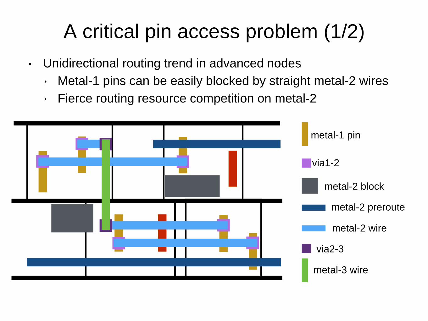
A critical pin access problem (1/2)
• Unidirectional routing trend in advanced nodes
‣ Metal-1 pins can be easily blocked by straight metal-2 wires
‣ Fierce routing resource competition on metal-2
metal-3 wire
metal-2 block
via1-2
via2-3
metal-2 wire
metal-1 pin
metal-2 preroute

A critical pin access problem (2/2)
• More restricted routing design rules in advanced nodes
‣ e.g., more space between vias
‣ e.g., metal layer patterns are compliant to SADP design rules
4

Improve pin access in different design stages
global placement
detailed placement
global routing
detailed routing
routability-driven
physical design flow
local congestion-aware
Pin access planning
5
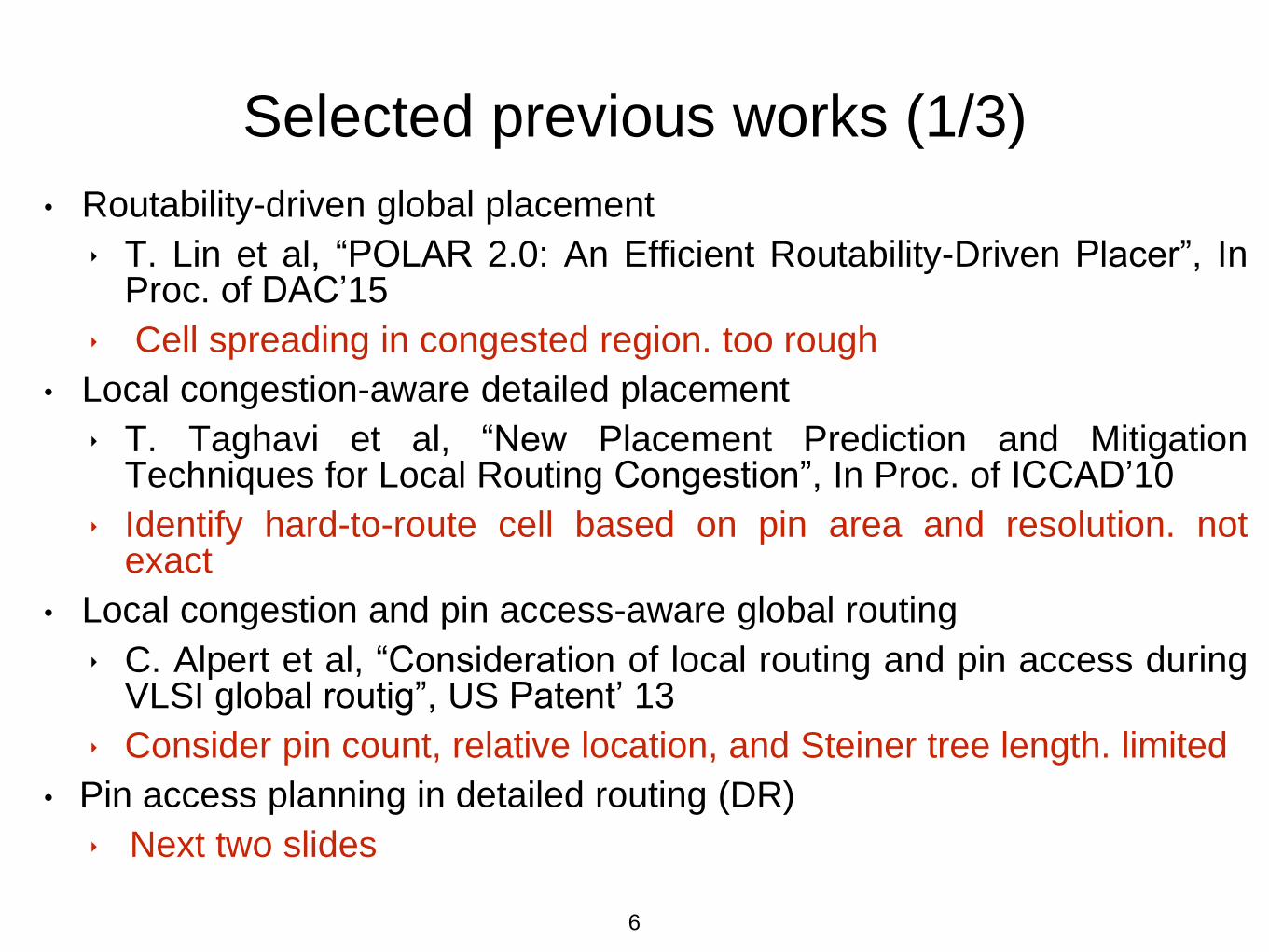
Selected previous works (1/3)
• Routability-driven global placement
‣ T. Lin et al, “POLAR 2.0: An Efficient Routability-Driven Placer”, InProc. of DAC’15
‣ Cell spreading in congested region. too rough
• Local congestion-aware detailed placement
‣ T. Taghavi et al, “New Placement Prediction and MitigationTechniques for Local Routing Congestion”, In Proc. of ICCAD’10
‣ Identify hard-to-route cell based on pin area and resolution. notexact
• Local congestion and pin access-aware global routing
‣ C. Alpert et al, “Consideration of local routing and pin access duringVLSI global routig”, US Patent’ 13
‣ Consider pin count, relative location, and Steiner tree length. limited
• Pin access planning in detailed routing (DR)
‣ Next two slides
6

Pin access planning in DR (1/2)
1. X. Xu et al, “PARR: Pin Access Planning and Regular Routing for Self-Aligned Double Patterning”, In Proc. of DAC’15
2. M. Ozdal et al, “Detailed-Routing Algorithms for Dense Pin Clusters in Integrated Circuits”, In TCAD’09
a bad planning a wise planning
A
B C
7

pin access planning in DR (2/2)
• It is not alway effective, especially in area with high pin density.
SCa SCb
• Movtivation: we want to resolve pin access issue here!
8
to improve pin
access/routability
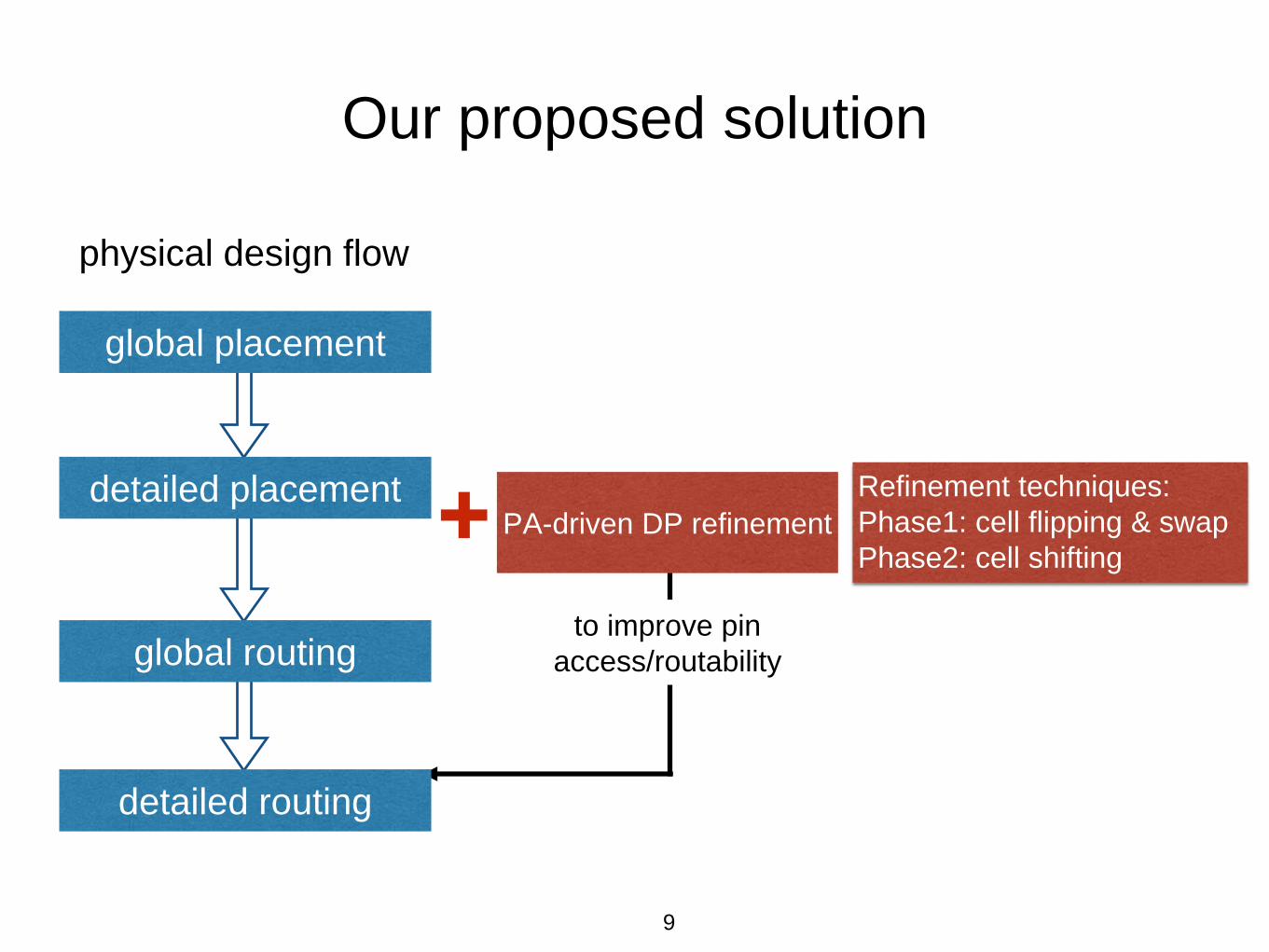
Our proposed solution
PA-driven DP refinement
Refinement techniques:
Phase1: cell flipping & swap
Phase2: cell shifting
global placement
detailed placement
global routing
detailed routing
physical design flow
9
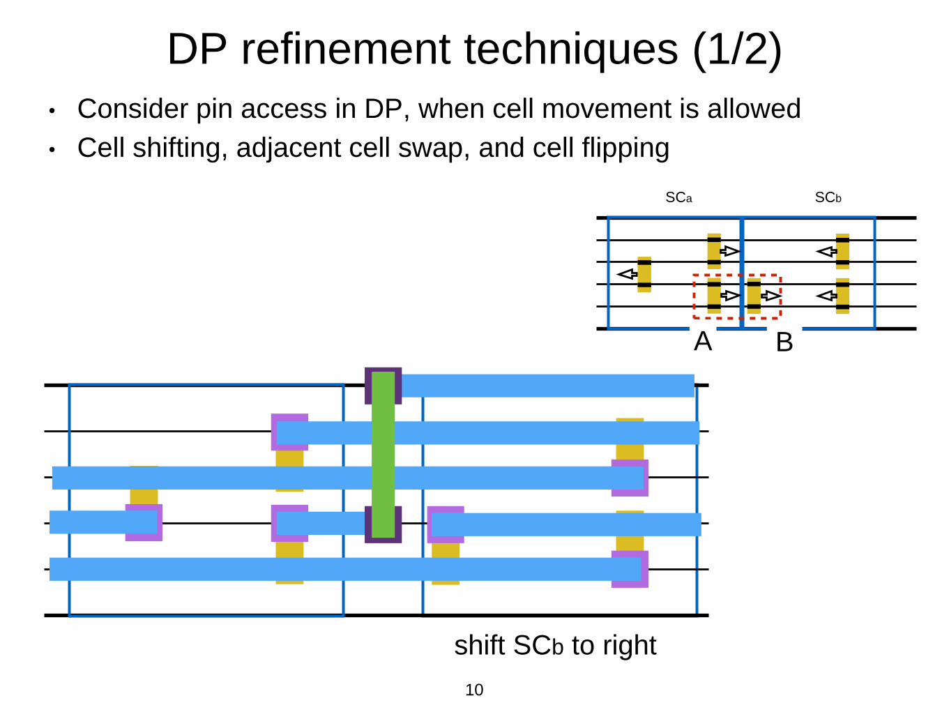
shift SCb to right
DP refinement techniques (1/2)
• Consider pin access in DP, when cell movement is allowed
• Cell shifting, adjacent cell swap, and cell flipping
SCbSCa
A B
10

flip SCb
DP refinement techniques (2/2)
SCbSCa
swap SCa and SCb
11

Our contributions
• It is the first work to directly consider pin access issue in detailed
placement (DP) stage
• An accurate model is proposed to capture pin access scenario in
detailed routing. A cost function is presented to guide DP
refinement to improve pin access
• Our DP refinemnt techniques are limited to cell flipping, adjacent
cell swap, and cell shifting. Our proposed solution is dynamic
programming and linear programming-based.
‣ Respect the given placement solution
‣ Gurantee good solution quality with fast runtime
• Experimental results demonstrates the effectiveness of our
proposed pin access-driven DP refinement
12
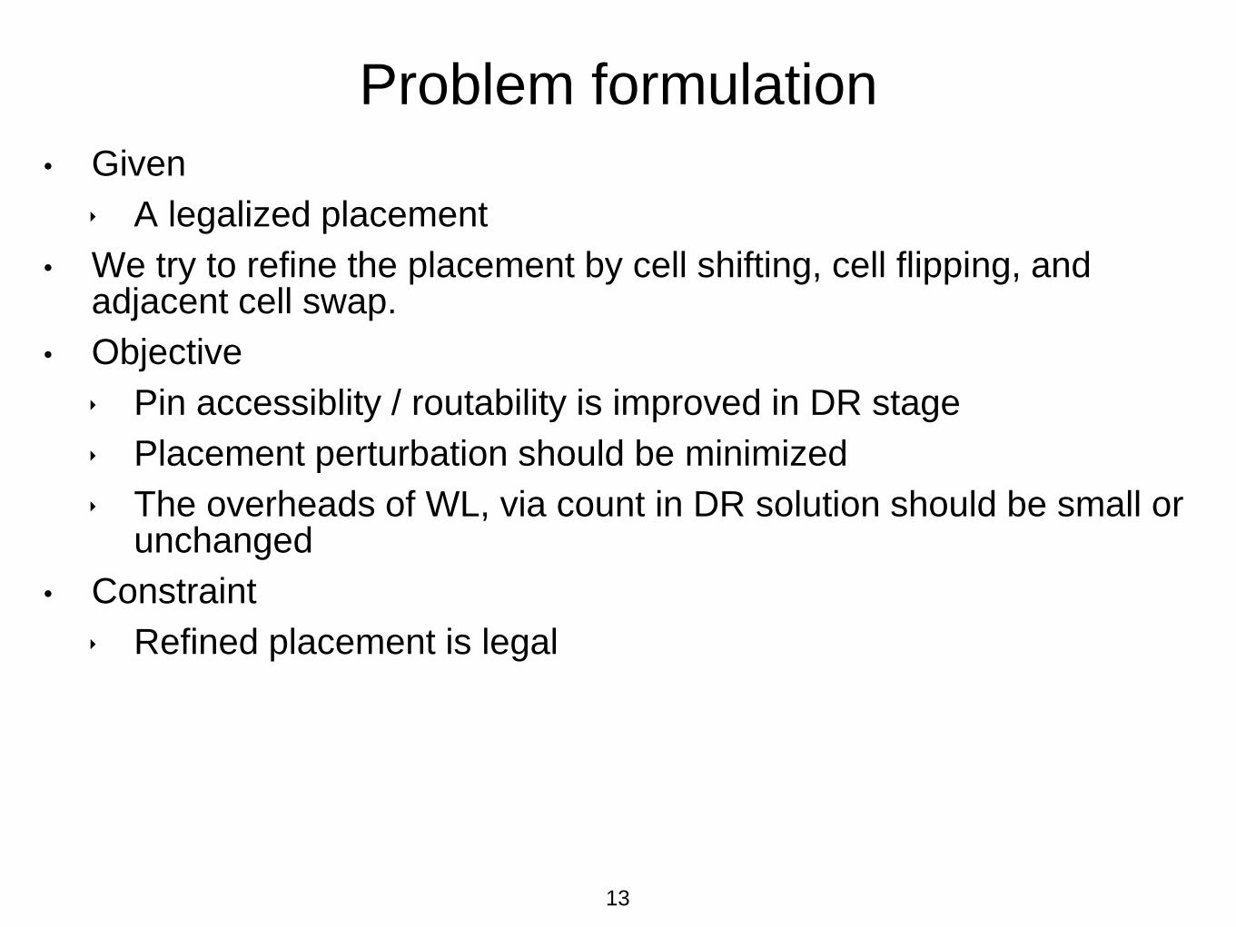
Problem formulation
• Given
‣ A legalized placement
• We try to refine the placement by cell shifting, cell flipping, and adjacent cell swap.
• Objective
‣ Pin accessiblity / routability is improved in DR stage
‣ Placement perturbation should be minimized
‣ The overheads of WL, via count in DR solution should be small or unchanged
• Constraint
‣ Refined placement is legal
13

Assumptions
• Each metal layer has a preferred routing direction.
‣ Metal1 is unroutable. metal2 horizontal, metal3 vertical…
• Standard cell (SC) ’s pins are rectlinear polygons on metal1. Each pinmay span several metal-2 tracks.
‣ The tapping point (TP) of a pin is defined as the overlap of metal-2 track and the pin shape
Pin access is to select a TP as a via location to connect metal-1 pin and
metal-2 wire segment such that the metal-2 wire segment can be extended
toward conn. dir. until the other connected pin.
14
TPconn.
dir.metal-2
track
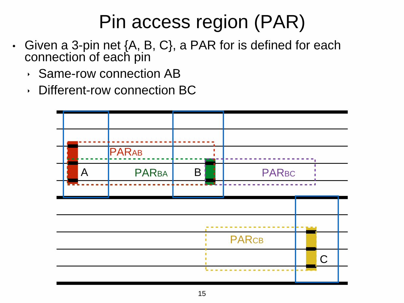
Pin access region (PAR)• Given a 3-pin net {A, B, C}, a PAR for is defined for each
connection of each pin
‣ Same-row connection AB
‣ Different-row connection BC
A B
C
PARAB
PARBA PARBC
PARCB
15

Pin access penalty (PAP) (1/3)
- penalty function • Objects (e.g., metal-2 block, wire segment) in PAR are penalized.
• Penalty function fw(dist)
same-row connection different-row connection
w
fw(dist)
1
dis
t minw
fw(dist)
1
wdis
t
min width of metal-2 wire
dist
w
16
Pin access penalty (PAP) (2/3)
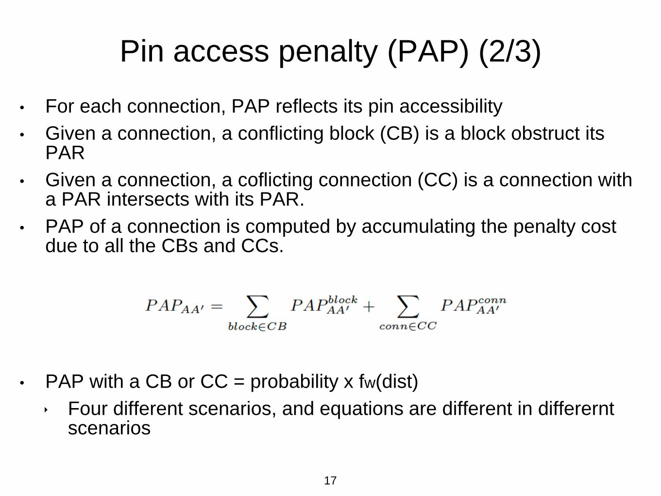
• For each connection, PAP reflects its pin accessibility
• Given a connection, a conflicting block (CB) is a block obstruct its PAR
• Given a connection, a coflicting connection (CC) is a connection with a PAR intersects with its PAR.
• PAP of a connection is computed by accumulating the penalty cost due to all the CBs and CCs.
• PAP with a CB or CC = probability x fw(dist)
‣ Four different scenarios, and equations are different in differernt scenarios
17

Pin access penalty (PAP) (3/3)
- four scenarios
(4)(3)
(2)(1)
18

Quantify the pin accessibilty of a DP
• For each connection, pin access penalty (PAP)
• For each cell c, cell pin access penalty (CPAP)
• For a DP, total cell pin access penalty (TCPAP)
• TCPAP reflects pin accessiblity of a DP, and should be minimized
19

Two-phase PA-driven DP refinement
pin accessibility-driven
placement refinement
Phase 1: cell flipping & cell swap
- dynamic programming row by row
Phase 2: cell shifting
- linear programming
legalized DP
refined legalized DP
20
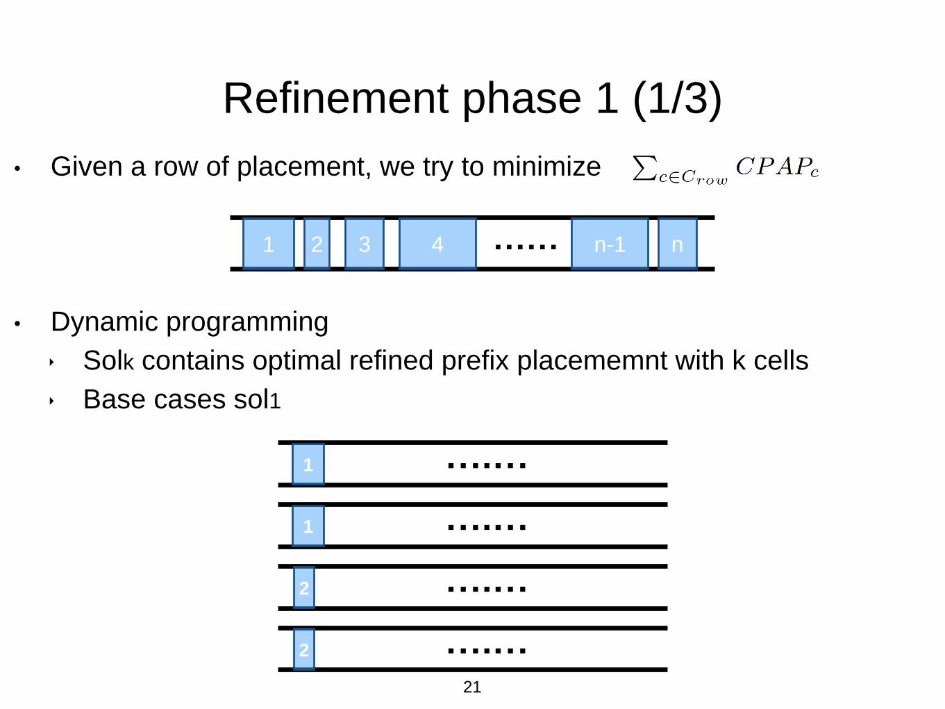
Refinement phase 1 (1/3)
• Given a row of placement, we try to minimize
• Dynamic programming
‣ Solk contains optimal refined prefix placememnt with k cells
‣ Base cases sol1
1 2 3 4 n-1 n……
….…1
….…1
….…2
….…2
21
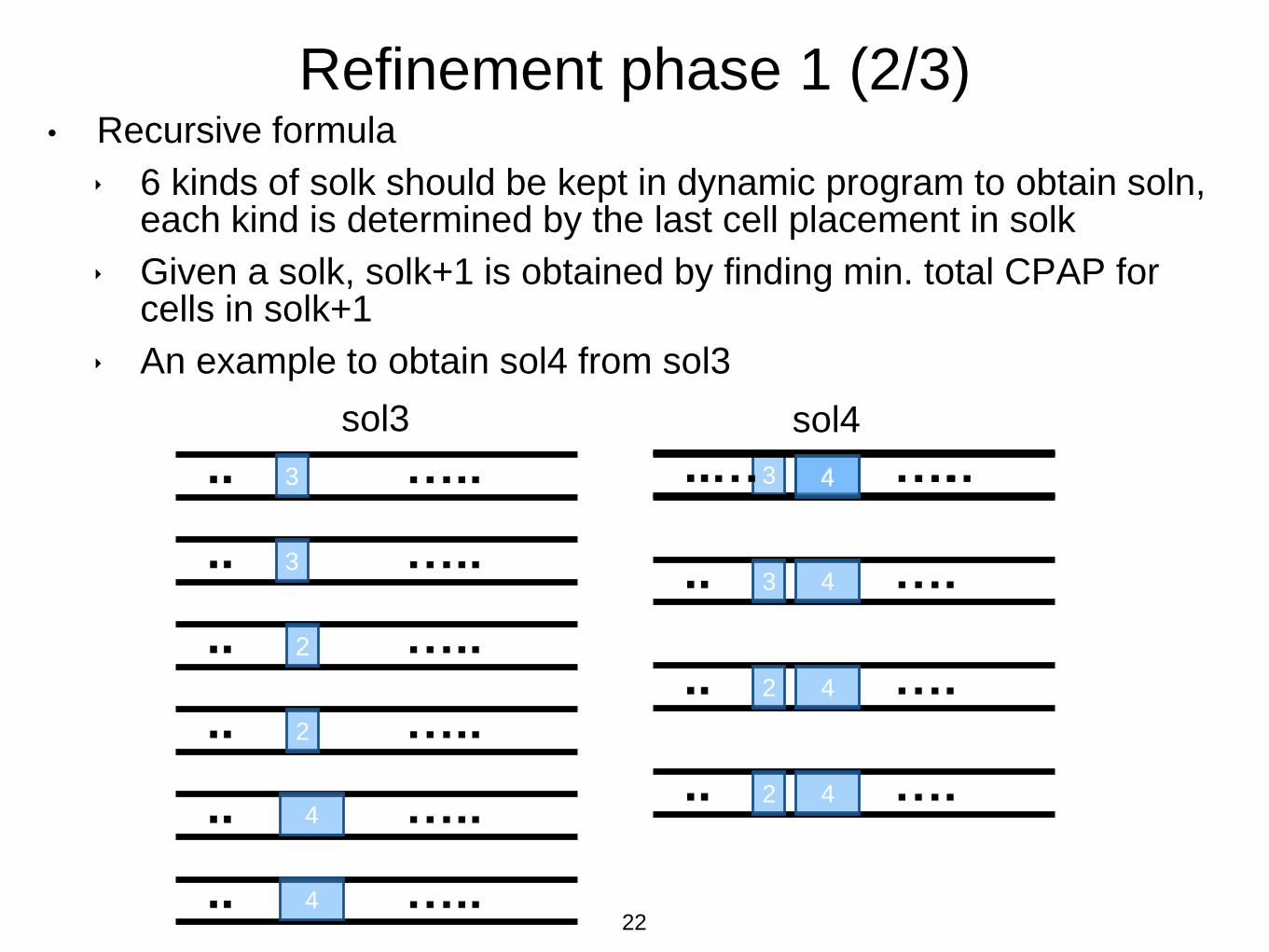
Refinement phase 1 (2/3)• Recursive formula
‣ 6 kinds of solk should be kept in dynamic program to obtain soln, each kind is determined by the last cell placement in solk
‣ Given a solk, solk+1 is obtained by finding min. total CPAP for cells in solk+1
‣ An example to obtain sol4 from sol3
sol4
3.. ….4
3.. ….4
2.. ….4
2.. ….4
4… ….
3.. …..
3.. …..
.. …..
2.. …..
4.. …..
4.. …..
sol3
2
22

Refinement phase 1 (3/3)
……. n
• Opt is obtained by finding min. total CPAP among 4 kinds of
soln
……. n
……. n-1
……. n-1
23

Refinement phase 2
• Objective: minimize TCPAP
‣ Linear approximation on penalty function
• Continuous variable denotes the x-location of each cell’s lowerleft corner
• controls the threshold of max cell shifting distance
• Linear constraints to ensure cells are not overlapped and out of LL & RR
LL RR
minw
fw(dist)
1
w dist
linear approximationTwo stdCell rows
24
Experimental set-up
• PA-driven DP refinemnt is implemented by C++.
• Experiments run on 2.4 GHz Intel Core i5 and 8GB memory.
• Gurobi 6.0 is called to solve linear program in phase 2.
• Original benchmarks are from [1].
‣ [1] X. Xu et al, “PARR: Pin Access Planning and Regular Routing for Self-Aligned Double Patterning”, In Proc. of DAC’15
• SADP-aware detailed router in [2] is called to route refined DP.
‣ [2] Y. Ding, et al, “Self-aligned double pattering lithography-aware detailed routing with color pre-assignment”, TCAD’16
• Two sets of experimental results are demonstrated:
‣ PA-DP refinement
‣ Detailed routing on refined placement
25

PA-driven DP refinement (1/2)
• Benchmark statistics
ecc efc ctl alu div top
#cells 1302 1197 1715 1802 3260 12576
0
10
20
30
40
50
ecc efc ctl alu div top
CP
U (
s)
Phase1&2 CPU
Phase1 CPU
0.60
0.70
0.80
0.90
1.00
ecc efc ctl alu div top
No
r. T
CP
AP
Given DP DP after P1 DP after P2
26
P1 ave. =0.85
P2 ave. =0.82

PA-driven DP refinement (2/2)
0.00
2.00
4.00
6.00
8.00
ecc efc ctl alu div top
Ave
. d
isp
lace
me
nt (p
itch
)
0.000
0.100
0.200
0.300
0.400
0.500
ecc efc ctl alu div top
Pct. flip
pe
d c
ell
27
P2 ave. =6.73
P1 ave. =5.04P1 ave. =0.33
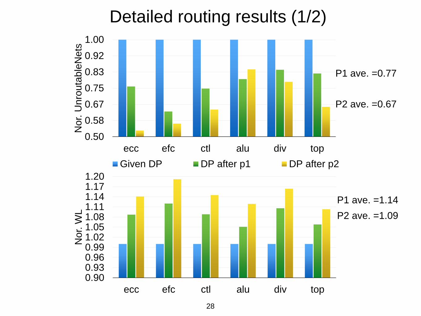
Detailed routing results (1/2)
0.900.930.960.991.021.051.081.111.141.171.20
ecc efc ctl alu div top
Nor.
WL
Given DP DP after p1 DP after p2
0.50
0.58
0.67
0.75
0.83
0.92
1.00
ecc efc ctl alu div top
Nor.
Unro
uta
ble
Nets
28
P1 ave. =0.77
P2 ave. =0.67
P1 ave. =1.14
P2 ave. =1.09
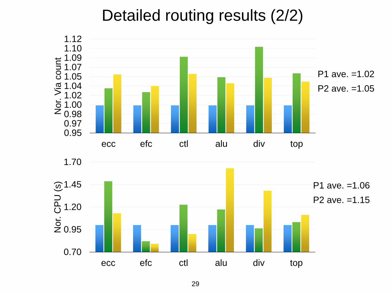
Detailed routing results (2/2)
0.70
0.95
1.20
1.45
1.70
ecc efc ctl alu div top
Nor.
CP
U (
s)
0.950.970.981.001.021.041.051.071.091.101.12
ecc efc ctl alu div top
Nor.
Via
count
29
P1 ave. =1.06
P2 ave. =1.15
P1 ave. =1.02
P2 ave. =1.05

Thank you!
Q & A
30


![Lens Aberration Aware Placement for Timing Yield · effects of resist and photo processes). Gupta et al. [2007] proposed a detailed placement technique to avoid forbidden pitch between](https://static.fdocuments.us/doc/165x107/604d4a68e9c1a430522f8ab5/lens-aberration-aware-placement-for-timing-yield-effects-of-resist-and-photo-processes.jpg)


