Pin 1 Reference Mark D 1 2 V C 50 MHz to 6000 MHz Digital ...
14
QPC3223 50 MHz to 6000 MHz Digital Step Attenuator Datasheet Rev. C, October 7, 2019 | Subject to change without notice 1 of 13 www.qorvo.com ® 12 Pad 3.0 mm x 3.0 mm QFN package Product Features • Frequency Range 50 MHz to 6000 MHz • 2-Bit, 18 dB Range, 6 dB Step • Overshoot-free Transient Switching Performance • High Linearity, Input IP3 > +55 dBm • Parallel Control Interface • Fast Switching Speed, 80 nsec Typical • Single Supply +3 V to +5 V Operation • 1.8V Logic Compatible • RF Pins Have No DC Voltage, Can be DC Grounded Externally • Patented Circuit Architecture • Power-up Default Setting Is Maximum Attenuation Applications • 2G through 4G Base Stations • Point-to-Point • Wi-Fi • Test Equipment Product Description The QPC3223 is a 2-bit digital step attenuator (DSA) that features high linearity over the entire 18 dB gain control range in 6 dB steps. The QPC3223 uses a parallel control interface and has a low insertion loss of 0.8 dB at 2 GHz. The patented circuit architecture provides overshoot-free transient switching performance using a single +3 V to +5 V power supply. The QPC3223 is available in an industry standard 12 pad 3 mm x 3 mm QFN package that is lead-free and RoHS- compliant Ordering Information Part No. Description QPC3223TR7 2500 pieces on a 7” reel QPC3223PCK401 50 – 6000 MHz PCBA w/5-pc. sample bag Functional Block Diagram Top View Pin 1 Reference Mark GND RFIN NC GND RFOUT NC V DD C1 C2 NC NC NC LOGIC CONTROL 2-BIT DSA 12 11 10 4 5 6 9 8 7 1 2 3
Transcript of Pin 1 Reference Mark D 1 2 V C 50 MHz to 6000 MHz Digital ...

QPC3223 50 MHz to 6000 MHz Digital Step Attenuator
Datasheet Rev. C, October 7, 2019 | Subject to change without notice 1 of 13 www.qorvo.com
®
12 Pad 3.0 mm x 3.0 mm QFN package
Product Features • Frequency Range 50 MHz to 6000 MHz
• 2-Bit, 18 dB Range, 6 dB Step
• Overshoot-free Transient Switching Performance
• High Linearity, Input IP3 > +55 dBm
• Parallel Control Interface
• Fast Switching Speed, 80 nsec Typical
• Single Supply +3 V to +5 V Operation
• 1.8V Logic Compatible
• RF Pins Have No DC Voltage, Can be DC Grounded
Externally
• Patented Circuit Architecture
• Power-up Default Setting Is Maximum Attenuation
Applications • 2G through 4G Base Stations
• Point-to-Point
• Wi-Fi
• Test Equipment
Product Description The QPC3223 is a 2-bit digital step attenuator (DSA) that
features high linearity over the entire 18 dB gain control
range in 6 dB steps. The QPC3223 uses a parallel control
interface and has a low insertion loss of 0.8 dB at 2 GHz.
The patented circuit architecture provides overshoot-free
transient switching performance using a single +3 V to +5 V
power supply.
The QPC3223 is available in an industry standard 12 pad
3 mm x 3 mm QFN package that is lead-free and RoHS-
compliant
Ordering Information Part No. Description
QPC3223TR7 2500 pieces on a 7” reel
QPC3223PCK401 50 – 6000 MHz PCBA w/5-pc. sample bag
Functional Block Diagram
Top View
Pin 1 Reference Mark
GND
RFIN
NC
GND
RFOUT
NC
VD
D
C1
C2
NC
NC
NC
LOGIC
CONTROL
2-BIT DSA
12 11 10
4 5 6
9
8
7
1
2
3

QPC3223
50 MHz to 6000 MHz Digital Step Attenuator
Datasheet Rev. C, October 7, 2019 | Subject to change without notice 2 of 13 www.qorvo.com
®
Recommended Operating Conditions Parameter Min Typ Max Units
Supply Voltage (VDD) +2.7 +5.5 V
Case Temperature −40 +105 °C
Operating Junction Temp. +125 °C
Electrical specifications are measured at specified test conditions. Specifications are not guaranteed over all recommended operating conditions.
Absolute Maximum Ratings Parameter Rating
Storage Temperature −40 to +150 °C
Supply Voltage (VDD) −0.5 to +6.0 V
All Other DC and Logic Pins (Supply Voltage
Must Be Applied Prior to Any Other Pin Voltages) −0.5 to +6.0 V
Input Power (RFIN Pin, +85°C Case Temp.) +30 dBm
Input Power (RFIN Pin, +105°C Case Temp.) +27 dBm
Input Power (RFOUT Pin, +85°C Case Temp.) +27 dBm
Input Power (RFOUT Pin, +105°C Case Temp.) +24 dBm
Exceeding any one or a combination of the Absolute Maximum Rating conditions may cause permanent damage to the device. Extended application of Absolute Maximum Rating conditions to the device may reduce device reliability.
Electrical Specifications Parameter Conditions Min Typ Max Units
Frequency Range 50 6000 MHz
Insertion Loss 2000 MHz, 0 dB Attenuation Setting 0.8 dB
Attenuation Range 0.25 dB step size 18 dB
Attenuation Step 6 dB
Attenuation Accuracy ± (0.2 + 4% of Atten. Setting) dB
Input IP3 +55 dBm
Input P0.1dB +30 dBm
RF Input Power at RFIN Pin Continuous operation at +85 °C case temperature +27 dBm
Continuous operation at +105 °C case temperature +24 dBm
RF Input Power at RFOUT Pin Continuous operation at +85 °C case temperature +20 dBm
Continuous operation at +105 °C case temperature +17 dBm
Return Loss 15 dB
Input and Output Impedance 50 Ω
Switching Speed 50% CTL to 10% / 90% RF 80 ns
Supply Current, IDD Steady state operation, current draw during attenuation state transitions is higher.
180 μA
Thermal Resistance At maximum attenuation state with RF power applied to the RFIN pin
62 °C/W
Notes: 1. Test conditions unless otherwise noted: VDD=+5 V, Temp= +25 °C, Freq.=2000 MHz, 50 Ω system,
Control Logic Requirements
Parameter Conditions Min Typ Max Units
Low State Input Voltage −0.2 +0.63 V
High State Input Voltage +1.17 VDD V
Notes: 1. Test conditions unless otherwise noted: VDD=+5 V, Temp= +25 °C, Freq.=2000 MHz, 50 Ω system,

QPC3223
50 MHz to 6000 MHz Digital Step Attenuator
Datasheet Rev. C, October 7, 2019 | Subject to change without notice 3 of 13 www.qorvo.com
®
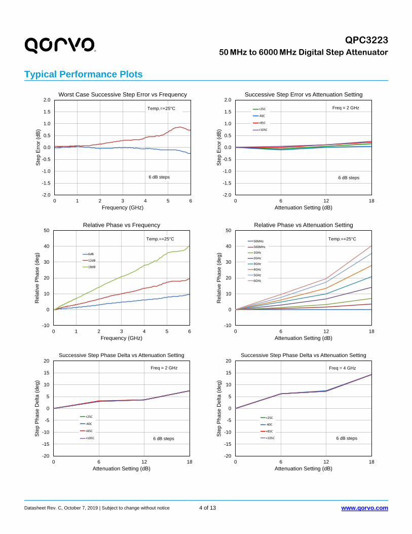
Typical Performance Plots
-5
-4
-3
-2
-1
0
0 1 2 3 4 5 6
Inse
rtio
n L
oss (
dB
)
Frequency (GHz)
Minimum Insertion Loss vs Frequency
+25C
-40C
+85C
+105C
-20
-18
-16
-14
-12
-10
-8
-6
-4
-2
0
0 6 12 18
Att
en
ua
tio
n (
dB
)
Attenuation Setting (dB)
Normalized Attenuation vs Attenuation Setting
50MHz
500MHz
1GHz
2GHz
3GHz
4GHz
5GHz
6GHz
Temp.=+25°C
-20
-18
-16
-14
-12
-10
-8
-6
-4
-2
0
0 1 2 3 4 5 6
Att
en
ua
tio
n (
dB
)
Frequency (GHz)
Normalized Attenuation vs Frequency
6dB
12dB
18dB
Temp.=+25°C
-2.0
-1.5
-1.0
-0.5
0.0
0.5
1.0
1.5
2.0
0 6 12 18
Att
en
ua
tio
n E
rro
r (d
B)
Attenuation Setting (dB)
Absolute Attenuation Error vs Attenuation Setting
50MHz
500MHz
1GHz
2GHz
3GHz
4GHz
5GHz
6GHz
Temp.=+25°C
-3
-2
-1
0
1
2
3
0 1 2 3 4 5 6
Att
en
ua
tio
n E
rro
r (d
B)
Frequency (GHz)
Major State Absolute Attenuation Error vs Frequency
6dB
12dB
18dB
Temp.=+25°C
-2.0
-1.5
-1.0
-0.5
0.0
0.5
1.0
1.5
2.0
0 6 12 18
Att
en
ua
tio
n E
rro
r (d
B)
Attenuation Setting (dB)
Absolute Attenuation Error vs Attenuation Setting
+25C
-40C
+85C
+105C
Freq = 2 GHz
QPC3223
50 MHz to 6000 MHz Digital Step Attenuator
Datasheet Rev. C, October 7, 2019 | Subject to change without notice 4 of 13 www.qorvo.com
®
Typical Performance Plots
-2.0
-1.5
-1.0
-0.5
0.0
0.5
1.0
1.5
2.0
0 1 2 3 4 5 6
Ste
p E
rro
r (d
B)
Frequency (GHz)
Worst Case Successive Step Error vs Frequency
Temp.=+25°C
6 dB steps
-2.0
-1.5
-1.0
-0.5
0.0
0.5
1.0
1.5
2.0
0 6 12 18
Ste
p E
rro
r (d
B)
Attenuation Setting (dB)
Successive Step Error vs Attenuation Setting
+25C
-40C
+85C
+105C
6 dB steps
Freq = 2 GHz
-10
0
10
20
30
40
50
0 1 2 3 4 5 6
Re
lative
Ph
ase
(d
eg
)
Frequency (GHz)
Relative Phase vs Frequency
6dB
12dB
18dB
Temp.=+25°C
-10
0
10
20
30
40
50
0 6 12 18
Re
lative
Ph
ase
(d
eg
)
Attenuation Setting (dB)
Relative Phase vs Attenuation Setting
50MHz
500MHz
1GHz
2GHz
3GHz
4GHz
5GHz
6GHz
Temp.=+25°C
-20
-15
-10
-5
0
5
10
15
20
0 6 12 18
Ste
p P
ha
se
De
lta
(d
eg
)
Attenuation Setting (dB)
Successive Step Phase Delta vs Attenuation Setting
+25C
-40C
+85C
+105C
Freq = 2 GHz
6 dB steps
-20
-15
-10
-5
0
5
10
15
20
0 6 12 18
Ste
p P
ha
se
De
lta
(d
eg
)
Attenuation Setting (dB)
Successive Step Phase Delta vs Attenuation Setting
+25C
-40C
+85C
+105C
Freq = 4 GHz
6 dB steps
QPC3223
50 MHz to 6000 MHz Digital Step Attenuator
Datasheet Rev. C, October 7, 2019 | Subject to change without notice 5 of 13 www.qorvo.com
®
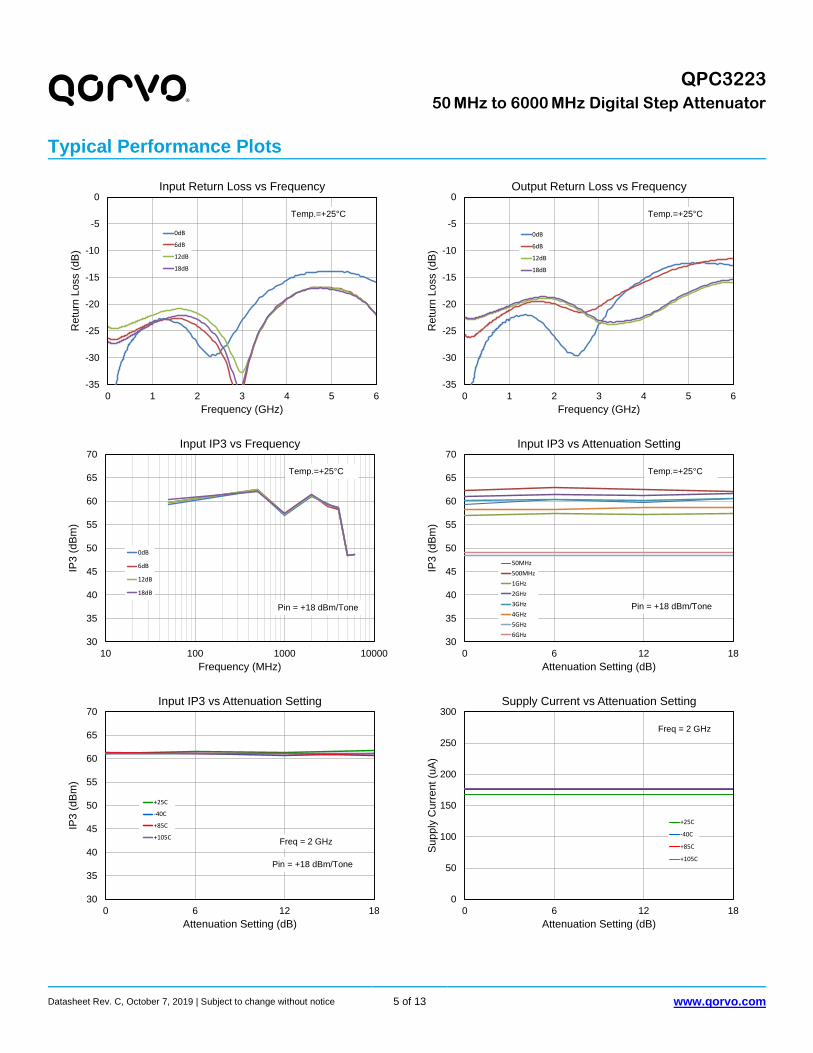
Typical Performance Plots
-35
-30
-25
-20
-15
-10
-5
0
0 1 2 3 4 5 6
Re
turn
Lo
ss (
dB
)
Frequency (GHz)
Input Return Loss vs Frequency
0dB
6dB
12dB
18dB
Temp.=+25°C
-35
-30
-25
-20
-15
-10
-5
0
0 1 2 3 4 5 6
Re
turn
Lo
ss (
dB
)
Frequency (GHz)
Output Return Loss vs Frequency
0dB
6dB
12dB
18dB
Temp.=+25°C
30
35
40
45
50
55
60
65
70
10 100 1000 10000
IP3
(d
Bm
)
Frequency (MHz)
Input IP3 vs Frequency
0dB
6dB
12dB
18dB
Temp.=+25°C
Pin = +18 dBm/Tone
30
35
40
45
50
55
60
65
70
0 6 12 18
IP3
(d
Bm
)
Attenuation Setting (dB)
Input IP3 vs Attenuation Setting
50MHz
500MHz
1GHz
2GHz
3GHz
4GHz
5GHz
6GHz
Temp.=+25°C
Pin = +18 dBm/Tone
30
35
40
45
50
55
60
65
70
0 6 12 18
IP3
(d
Bm
)
Attenuation Setting (dB)
Input IP3 vs Attenuation Setting
+25C
-40C
+85C
+105C
Pin = +18 dBm/Tone
Freq = 2 GHz
0
50
100
150
200
250
300
0 6 12 18
Su
pp
ly C
urr
en
t (u
A)
Attenuation Setting (dB)
Supply Current vs Attenuation Setting
+25C
-40C
+85C
+105C
Freq = 2 GHz
QPC3223
50 MHz to 6000 MHz Digital Step Attenuator
Datasheet Rev. C, October 7, 2019 | Subject to change without notice 6 of 13 www.qorvo.com
®
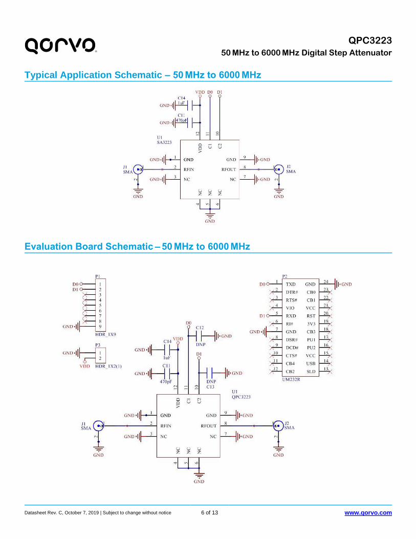
Typical Application Schematic – 50 MHz to 6000 MHz
Evaluation Board Schematic – 50 MHz to 6000 MHz
QPC3223
50 MHz to 6000 MHz Digital Step Attenuator
Datasheet Rev. C, October 7, 2019 | Subject to change without notice 7 of 13 www.qorvo.com
®
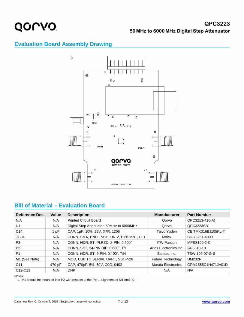
Evaluation Board Assembly Drawing
Bill of Material – Evaluation Board Reference Des. Value Description Manufacturer Part Number
N/A N/A Printed Circuit Board Qorvo QPC3213-410(A)
U1 N/A Digital Step Attenuator, 50MHz to 6000MHz Qorvo QPC3223SB
C14 1 μF CAP, 1µF, 10%, 25V, X7R, 1206 Taiyo Yuden CE TMK316BJ105KL-T
J1-J4 N/A CONN, SMA, END LNCH, UNIV, HYB MNT, FLT Molex SD-73251-4000
P3 N/A CONN, HDR, ST, PLRZD, 2-PIN, 0.100” ITW Pancon MPSS100-2-C
P2 N/A CONN, SKT, 24-PIN DIP, 0.600”, T/H Aries Electronics Inc. 24-6518-10
P1 N/A CONN, HDR, ST, 9-PIN, 0.100”, T/H Samtec Inc. TSW-109-07-G-S
M1 (See Note) N/A MOD, USB TO SERIAL UART, SSOP-28 Future Technology UM232R
C11 470 pF CAP, 470pF, 5%, 50V, C0G, 0402 Murata Electronics GRM1555C1H471JA01D
C12-C13 N/A DNP N/A N/A
Notes: 1. M1 should be mounted into P2 with respect to the Pin 1 alignment of M1 and P2.
QPC3223
50 MHz to 6000 MHz Digital Step Attenuator
Datasheet Rev. C, October 7, 2019 | Subject to change without notice 8 of 13 www.qorvo.com
®
Evaluation Board Programming Using USB Interface
Parallel Mode
Refer to the Control Bit Generator (CBG) Software Reference Manual for detailed instructions on how to setup the software
for use. Apply the supply voltage to P3. Select ‘QPC3223’ from the Parts List of the CBG user interface. Set the attenuation
value using the CBG user interface. The attenuator is set to the desired state and measurements can be taken.
Evaluation Board Programming Using External Bus
Parallel Mode
This configuration allows the user to control the attenuator through the P1 connector using an external harness. Remove
the USB interface if it is currently installed on the evaluation board. Connect a user-supplied harness to the P1 connector.
The parallel bus signal names for P1 are indicated on the evaluation board. Cross reference for device pins names to P1
connector signals is as follows: C1 = D0, C2 = D1. Apply the supply voltage to P3. Send the appropriate signals onto the
parallel bus lines in accordance with the Parallel Interface Attenuation Truth Table. The attenuator is set to the desired
state and measurements can be taken.
Default Power-up State
The default attenuation state is maximum (18dB) when supply voltage is applied to the attenuator. If a different attenuation
state is desired during power up, this can be accomplished by applying signals according to the Parallel Interface
Attenuation Truth Table. The attenuator will power up to the state applied to the parallel bus during turn on.
Parallel Interface Attenuation Truth Table Attenuation Word
Attenuation State C1 (D0) C2 (D1)
L L 0dB / Reference Insertion Loss
H L 6 dB
L H 12 dB
H H 18 dB

QPC3223
50 MHz to 6000 MHz Digital Step Attenuator
Datasheet Rev. C, October 7, 2019 | Subject to change without notice 9 of 13 www.qorvo.com
®
Pad Configuration and Description
Top View
Pad No. Label Description
1 GND Ground Pin; Connect to PCB ground
2 RFIN RF Input Pin; Incident RF power must enter this pin for rated thermal performance and reliability. Do not apply DC power to this pin. Pin may be DC grounded externally and is grounded thru resistors internal to the part.
3 NC Open in package. Connect to PCB ground or leave floating
4 NC Open in package. Connect to PCB ground or leave floating
5 NC Open in package. Connect to PCB ground or leave floating
6 NC Open in package. Connect to PCB ground or leave floating
7 NC Open in package. Connect to PCB ground or leave floating
8 RFOUT RF Output Pin; Pin may be DC grounded externally and is grounded thru resistors internal to the part.
9 GND Ground Pin; Connect to PCB ground
10 C2 12dB bit parallel logic input; 1.8V CMOS compatible logic
11 C1 6dB bit parallel logic input; 1.8V CMOS compatible logic
12 VDD Supply Voltage
Backside Pad GND RF/DC ground. Use recommended via pattern to minimize inductance and thermal resistance. See PCB Mounting Pattern for suggested footprint.
Backside Pad - RF/DC GND
Pin 1 Reference Mark
GND
RFIN
NC
GND
RFOUT
NC
VD
D
C1
C2
NC
NC
NC
12 11 10
4 5 6
9
8
7
1
2
3

QPC3223
50 MHz to 6000 MHz Digital Step Attenuator
Datasheet Rev. C, October 7, 2019 | Subject to change without notice 10 of 13 www.qorvo.com
®
Package Dimensions
Notes: 1. All Dimensions in millimeters
Branding Diagram
QPC3223
50 MHz to 6000 MHz Digital Step Attenuator
Datasheet Rev. C, October 7, 2019 | Subject to change without notice 11 of 13 www.qorvo.com
®
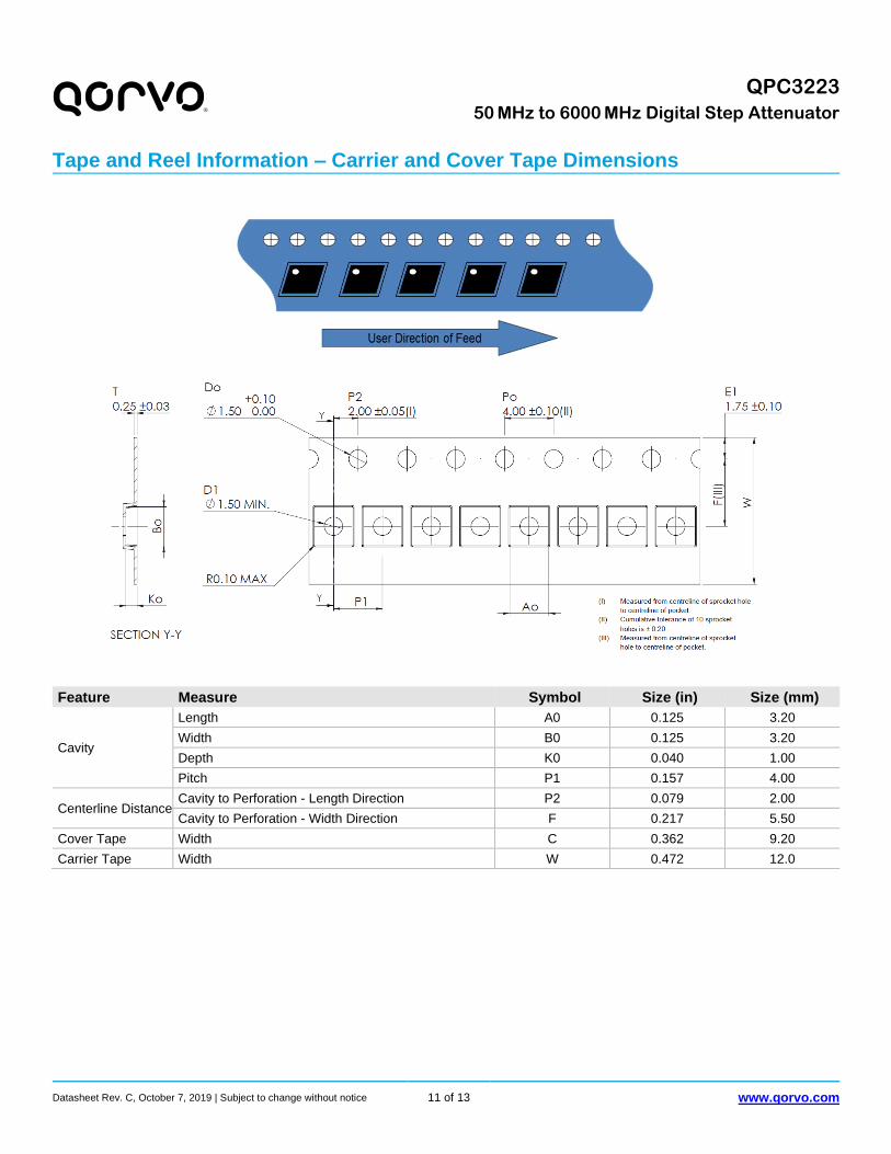
Tape and Reel Information – Carrier and Cover Tape Dimensions
Feature Measure Symbol Size (in) Size (mm)
Cavity
Length A0 0.125 3.20
Width B0 0.125 3.20
Depth K0 0.040 1.00
Pitch P1 0.157 4.00
Centerline Distance Cavity to Perforation - Length Direction P2 0.079 2.00
Cavity to Perforation - Width Direction F 0.217 5.50
Cover Tape Width C 0.362 9.20
Carrier Tape Width W 0.472 12.0

QPC3223
50 MHz to 6000 MHz Digital Step Attenuator
Datasheet Rev. C, October 7, 2019 | Subject to change without notice 12 of 13 www.qorvo.com
®
Tape and Reel Information – Reel Dimensions
Standard T/R size = 2,500 pieces on a 7” reel.
Feature Measure Symbol Size (in) Size (mm)
Flange
Diameter A 6.969 177.0
Thickness W2 0.717 18.2
Space Between Flange W1 0.504 12.8
Hub
Outer Diameter N 2.283 58.0
Arbor Hole Diameter C 0.512 13.0
Key Slit Width B 0.079 2.0
Key Slit Diameter D 0.787 20.0
Tape and Reel Information – Tape Length and Label Placement
Notes: 1. Empty part cavities at the trailing and leading ends are sealed with cover tape. See EIA 481-1-A. 2. Labels are placed on the flange opposite the sprockets in the carrier tape.
QPC3223
50 MHz to 6000 MHz Digital Step Attenuator
Datasheet Rev. C, October 7, 2019 | Subject to change without notice 13 of 13 www.qorvo.com
®
Handling Precautions Parameter Rating Standard
Caution! ESD-Sensitive Device
ESD – Human Body Model (HBM) Class 1C ANSI / ESDA / JEDEC JS-001-2014
ESD – Human Body Model (CDM) Class C3 ANSI / ESDA / JEDEC JS-002-2014
MSL – Moisture Sensitivity Level Level 2 IPC / JEDEC J-STD-020
Contact Information For the latest specifications, additional product information, worldwide sales and distribution locations:
Web: www.qorvo.com
Tel: 1-844-890-8163
Email: [email protected]
Important Notice The information contained herein is believed to be reliable; however, Qorvo makes no warranties regarding the information contained herein and assumes no responsibility or liability whatsoever for the use of the information contained herein. All information contained herein is subject to change without notice. Customers should obtain and verify the latest relevant information before placing orders for Qorvo products. The information contained herein or any use of such information does not grant, explicitly or implicitly, to any party any patent rights, licenses, or any other intellectual property rights, whether with regard to such information itself or anything described by such information. THIS INFORMATION DOES NOT CONSTITUTE A WARRANTY WITH RESPECT TO THE PRODUCTS DESCRIBED HEREIN, AND QORVO HEREBY DISCLAIMS ANY AND ALL WARRANTIES WITH RESPECT TO SUCH PRODUCTS WHETHER EXPRESS OR IMPLIED BY LAW, COURSE OF DEALING, COURSE OF PERFORMANCE, USAGE OF TRADE OR OTHERWISE, INCLUDING THE IMPLIED WARRANTIES OF MERCHANTABILITY AND FITNESS FOR A PARTICULAR PURPOSE.
Without limiting the generality of the foregoing, Qorvo products are not warranted or authorized for use as critical components in medical, life-saving, or life-sustaining applications, or other applications where a failure would reasonably be expected to cause severe personal injury or death.
Copyright 2019 © Qorvo, Inc. | Qorvo is a registered trademark of Qorvo, Inc.
Solderability Compatible with both lead-free (260°C max. reflow temp.) and tin/lead (245°C max. reflow temp.) soldering processes.
Solder profiles available upon request.
Contact plating: NiPdAu
RoHS Compliance This part is compliant with 2011/65/EU RoHS directive (Restrictions on the Use of Certain Hazardous Substances in Electrical and Electronic Equipment) as amended by Directive 2015/863/EU. This product also has the following attributes:
• Lead Free
• Halogen Free (Chlorine, Bromine) • Antimony Free
• TBBP-A (C15H12Br402) Free
• PFOS Free
• SVHC Free
Pb

Mouser Electronics
Authorized Distributor
Click to View Pricing, Inventory, Delivery & Lifecycle Information: Qorvo:
QPC3223SR QPC3223TR7 QPC3223 QPC3223PCK401


![· 30/09/2009 · - Pin Count[Pins] 및Data Rate[MHz]에따라구분하여100만원에서200만원까지차등부과 ※웨이퍼와패키지시험동시의뢰시50% 할인, 시험프로그램변경이없을시재시험1회무료](https://static.fdocuments.us/doc/165x107/5ed8bbcb6714ca7f4768786a/30092009-pin-countpins-edata-ratemhzeeee100eoeoe200eoeeoeeee.jpg)